SN74AHC1G125DCKT - Electronic component TEXAS INSTRUMENTS - Free user manual and instructions
Find the device manual for free SN74AHC1G125DCKT TEXAS INSTRUMENTS in PDF.

User questions about SN74AHC1G125DCKT TEXAS INSTRUMENTS
0 question about this device. Answer the ones you know or ask your own.
Ask a new question about this device
Download the instructions for your Electronic component in PDF format for free! Find your manual SN74AHC1G125DCKT - TEXAS INSTRUMENTS and take your electronic device back in hand. On this page are published all the documents necessary for the use of your device. SN74AHC1G125DCKT by TEXAS INSTRUMENTS.
USER MANUAL SN74AHC1G125DCKT TEXAS INSTRUMENTS
SN74AHC1G125SingleBusBufferGateWith3-StateOutput
1Features3Description
- OperatingRangeof2Vto5.5V
•Maxt pd of6nsat5V
•LowPowerConsumption,10-μAMaxI cc - ±8-mAOutputDriveat5V
2Applications
- Projectors
•TVs
•Servers
•MotorControls:ACInduction
•PatientMonitoring
•ElectronicPointsofSale
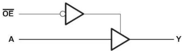
4SimplifiedSchematic
TheSN74AHC1G125deviceisasinglebusbuffer gate/linedriverwith3-stateoutput.Theoutputis disabledwhentheoutput-enable(OE)inputishigh.WhenOEislow,truedataispassedfromtheAinput totheYoutput.
DeviceInformation (1)
| PARTNUMBER | PACKAGE | BODYSIZE(NOM) |
| SN74AHC1G125 | SOT-23(5) | 2.90mmx1.60mm |
| SC-70(5) | 2.00mmx1.30mm | |
| SOT-553(5) | 1.65mmx1.20mm |
(1) For all available packages, see the orderable addendum at the endofthedatasheet.
text_image
OE A YTableofContents
1 Features.... 1
2 Applications 1
3 Description 1
4SimplifiedSchematic....1
5 Revision History...... 2
6PinConfigurationandFunctions....3
7 Specifications.... 4
7.1 AbsoluteMaximumRatings....4
7.2ESDRatings....4
7.3RecommendedOperatingConditions....4
7.4ThermalInformation....5
7.5 Electrical Characteristics....5
7.6SwitchingCharacteristics, V CC =3.3V±0.3V......5
7.7SwitchingCharacteristics,V CC =5V±0.5V......6
7.8OperatingCharacteristics....6
7.9TypicalCharacteristics....6
8ParameterMeasurementInformation....7
9 Detailed Description 8
9.1Overview....8
9.2FunctionalBlockDiagram....8
9.3FeatureDescription....8
9.4DeviceFunctionalModes....8
10ApplicationandImplementation....9
10.1 Application Information....9
10.2TypicalApplication....9
11PowerSupplyRecommendations....10
12 Layout.... 11
12.1 LayoutGuidelines....11
12.2LayoutExample....11
13DeviceandDocumentationSupport....11
13.1 Trademarks....11
13.2ElectrostaticDischargeCaution....11
13.3Glossary....11
14Mechanical, Packaging, and Orderable Information 11
5RevisionHistory
ChangesfromRevisionJ(June2005)toRevisionKPage
- Added Applications, Device Information table, Pin Functions table, ESD Ratings table, Thermal Information table, Typical Characteristics, Feature Description section, Device Functional Modes, Application and Implementation section, Power Supply Recommendations section, Layout section, Device and Documentation Support section, and Mechanical, Packaging, and Orderable Information section.... 1
- Deleted Ordering Information table. 1
- Changed MAX operating temperature to 125°C in Recommended Operating Conditions table. 4
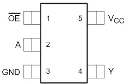
6PinConfigurationandFunctions
DBV PACKAGE
(TOP VIEW)
text_image
OE 1 5 VCC A 2 GND 3 4 YDCK PACKAGE
(TOP VIEW)

text_image
OE 1 5 VCC A 2 GND 3 4 YDRL PACKAGE
(TOP VIEW)
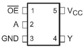
text_image
OE 1 5 VCC A 2 GND 3 4 YSee mechanical drawings for dimensions.
PinFunctions
| PIN | TYPEDE | SCRIPTION | |
| NO.NAME | |||
| 1OEI | |||
| 2A | I InputA | ||
| 3 | GND | — | GroundPin |
| 4Y | O OutputY | ||
| 5 | V_CC | — | PowerPin |
7Specifications
7.1 AbsoluteMaximumRatings (1)
overoperatingfree-airtemperaturerange(unlessotherwisenoted)
| MINMAXUNIT | ||||
| V_CC | Supplyvoltagerange-0.57V | |||
| V_I | Inputvoltagerange(2) | -0.57V | ||
| V_O | Outputvoltagerange(2) | -0.5V CC+0.5V | ||
| I_IK | InputclampcurrentV | I<0-20 mA | ||
| I_OK | Outputclampcurrent | VO<0orVO>VCC | ±20 | mA |
| I_O | Continuousoutputcurrent | VO=0toV CC | ±25 | mA |
| ContinuouschannelcurrentthroughV CC orGND | ±50 | mA | ||
| T_stg | Storagetemperaturerange | -65 150 | °C | |
(1) Stresses beyond those listed under Absolute Maximum Ratings may cause permanent damage to the device. These are stress ratings only, and functional operation of the device at these or any other conditions beyond those indicated under Recommended Operating Conditions is not implied. Exposure to absolute-maximum-rated conditions for extended periods may affect device reliability.
(2) The input and output voltage ratings may be exceeded if the input and output current ratings are observed.
7.2ESDRatings
| VALUEUNIT | |||
| V_(ESD) Electrostaticdischarge | Humanbodymodel(HBM),perANSI/ESDA/JEDECJS-001,allpins (1) | 1500 | V |
| Chargeddevicemodel(CDM),perJEDECspecificationJESD22-C101, allpins (2) | 2000 | ||
(1) JEDEC document JEP155 states that 500-V HBM allows safe manufacturing with a standard ESD control process.
(2) JEDEC document JEP157 states that 250-V CDM allows safe manufacturing with a standard ESD control process.
7.3 Recommended Operating Conditions
overoperatingfree-airtemperaturerange(unlessotherwisenoted) (1)
| MIN | MAX | UNIT | |||
| V_CC | Supplyvoltage | 2 | 5.5 | V | |
| V_IH | High-levelinputvoltage | V_CC=2V | 1.5 | V | |
| V_CC=3V | 2.1 | ||||
| V_CC=5.5V | 3.85 | ||||
| V_IL | Low-levelinputvoltage | V_CC=2V | 0.5 | V | |
| V_CC=3V | 0.9 | ||||
| V_CC=5.5V | 1.65 | ||||
| V_I | Inputvoltage | 0 | 5.5 | V | |
| V_O | Outputvoltage | 0 | V_CC | V | |
| I_OH | High-leveloutputcurrent | V_CC=2V | -50 | μA | |
| V_CC=3.3V±0.3V-4 | mA | ||||
| V_CC=5V±0.5V | -8 | ||||
| I_OL | Low-leveloutputcurrent | V_CC=2V | 50 | μA | |
| V_CC=3.3V±0.3V | 4 | mA | |||
| V_CC=5V±0.5V | 8 | ||||
| t/ v | Input transition rise or fall rate | V_CC=3.3V±0.3V | 100 | ns/V | |
| V_CC=5V±0.5V | 20 | ||||
| T_A | Operating free-air temperature | -40 | 125 | °C | |
(1) AllunusedinputsofthedevicemustbeheldatV CC or GNDtoensureproperdeviceoperation. RefertotheTlapplicationreport, ImplicationsofSloworFloatingCMOSInputs(SCBA004).
7.4ThermalInformation
| THERMALMETRIC (1) | SN74AHC1G125 | ||||
| DBVDCKDRLUNIT | |||||
| 5PINS | |||||
| R_ JA | Junction-to-ambientthermalresistance231.3287.6328.7 | ||||
| R_ JC(top) | Junction-to-case(top)thermalresistance119.997.7105.1 | ||||
| R_ JB | Junction-to-boardthermalresistance60.665.150.3 °C/W | ||||
| _JT | Junction-to-topcharacterizationparameter | 17.82.0 | 6.9 | ||
| _JB | Junction-to-boardcharacterizationparameter | 60.164.214$ .4 | |||
(1) For more information about traditional and new thermal metrics, see the IC Package Thermal Metrics application report (SPRA953).
7.5 Electrical Characteristics
over recommended operating free-air temperature range (unless otherwise noted)
| PARAMETER | TESTCONDITIONS | V_cc | T_A =25°C | -40°Cto85°C | -40°Cto125°C | UNIT | ||||
| MIN | TYP | MAX | MIN | MAX | MIN | MAX | ||||
| V_OH | I_OH=-50 μA | 2 V | 1.9 | 2 | 1.9 | 1.9 | V | |||
| 3 V | 2.9 | 3 | 2.9 | 2.9 | ||||||
| 4.5 V | 4.4 | 4.5 | 4.4 | 4.4 | ||||||
| I_OH=-4 mA | 3 V | 2.58 | 2.48 | 2.48 | ||||||
| I_OH=-8 mA | 4.5 V | 3.94 | 3.8 | 3.8 | ||||||
| V_OL | I_OL=50 μA | 2V | 0.1 | 0.1 | 0.1 | V | ||||
| 3 V | 0.1 | 0.1 | 0.1 | |||||||
| 4.5 V | 0.1 | 0.1 | 0.1 | |||||||
| I_OL=4 mA | 3 V | 0.36 | 0.44 | 0.44 | ||||||
| I_OL=8 mA | 4.5 V | 0.36 | 0.44 | 0.44 | ||||||
| I_I | V_I=5.5 V or GND | 0Vto 5.5V | ±0.1 | ±1 | ±1 | μA | ||||
| I_OZ | V_I=V_CC or GND | 5.5 V | ±0.25 | ±2.5 | ±2.5 | μA | ||||
| I_CC | V_I=V_CC orGND, I_O=0 | 5.5 V | 1 | 10 | 10 | μA | ||||
| C_i | V_I=V_CC or GND | 5 V | 4 | 10 | 10 | 10 | pF | |||
| C_o | V_O=V_CC orGND | 5V | 10 | pF | ||||||
7.6SwitchingCharacteristics,V cc =3.3V±0.3V
over recommended operating free-air temperature range (unless otherwise noted) (see Figure 3)
| PARAMETER | FROM(INPUT) | TO(OUTPUT) | LOADCAPACITANCE | T_A=25°C | -40°Cto85°C | -40°Cto125°C | UNIT | ||||
| MIN | TYP | MAX | MIN | MAX | MIN | MAX | |||||
| t_PLH | A | Y | C_L=15pF | 5.6 | 8 | 1 | 9.5 | 1 | 10.5 | ns | |
| t_PHL | 5.6 | 8 | 1 | 9.5 | 1 | 10.5 | |||||
| t_PZH | Y | C_L=15pF | 5.4 | 8 | 1 | 9.5 | 1 | 10.5 | ns | ||
| t_PZL | 5.4 | 8 | 1 | 9.5 | 1 | 10.5 | |||||
| t_PHZ | Y | C_L=15pF | 7 | 9.7 | 1 | 11.5 | 1 | 12.5 | ns | ||
| t_PLZ | 7 | 9.7 | 1 | 11.5 | 1 | 12.5 | |||||
| t_PLH | A | Y | C_L=50pF | 8.1 | 11.5 | 1 | 13 | 1 | 14 | ns | |
| t_PHL | 8.1 | 11.5 | 1 | 13 | 1 | 14 | |||||
| t_PZH | Y | C_L=50pF | 7.9 | 11.5 | 1 | 13 | 1 | 14 | ns | ||
| t_PZL | 7.9 | 11.5 | 1 | 13 | 1 | 14 | |||||
| t_PHZ | Y | C_L=50pF | 9.5 | 13.2 | 1 | 15 | 1 | 16 | ns | ||
| t_PLZ | 9.5 | 13.2 | 1 | 15 | 1 | 16 | |||||
7.7SwitchingCharacteristics,V cc =5V±0.5V
overrecommendedoperatingfree-airtemperaturerange(unlessotherwisenoted)(seeFigure3)
| PARAMETER | FROMTO(INPUT) | LOAD(OUTPUT) | CAPACITANCE | T_A =25°C-40°Cto85°C-40°Cto125°C | UNIT | ||||||
| MIN | TYP | MAX | MINMAXMINMAX | ||||||||
| t_PLH | A | YC | L=15pF | 3.8 | 5.5 | 1 | 6.5 | 1 | 7 | ns | |
| t_PHL | 3.8 | 5.5 | 1 | 6.5 | 1 | 7 | |||||
| t_PZH | YC | L=15pF | 3.6 | 5.1 | 1 | 6 | 1 | 6.5 | ns | ||
| t_PZL | 3.6 | 5.1 | 1 | 6 | 1 | 6.5 | |||||
| t_PHZ | YC | L=15pF | 4.6 | 6.8 | 1 | 8 | 1 | 8.5 | ns | ||
| t_PLZ | 4.6 | 6.8 | 1 | 8 | 1 | 8.5 | |||||
| t_PLH | A | YC | L=50pF | 5.3 | 7.5 | 1 | 8.5 | 1 | 9.5 | ns | |
| t_PHL | 5.3 | 7.5 | 1 | 8.5 | 1 | 9.5 | |||||
| t_PZH | YC | L=50pF | 5.1 | 7.1 | 1 | 8 | 1 | 9 | ns | ||
| t_PZL | 5.1 | 7.1 | 1 | 8 | 1 | 9 | |||||
| t_PHZ | YC | L=50pF | 6.1 | 8.8 | 1 | 10 | 1 | 11 | ns | ||
| t_PLZ | 6.1 | 8.8 | 1 | 10 | 1 | 11 | |||||
7.8 Operating Characteristics
V_CC=5V,T A=25°C
| PARAMETER | TEST CONDITIONS | TYP | UNIT | |
| C_pd | Power dissipation capacitance | No load, f = 1 MHz | 14 | pF |
7.9TypicalCharacteristics
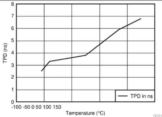
line
| Temperature (°C) | TPD (ns) | | ---------------- | -------- | | -100 | 2.5 | | 0 | 3.0 | | 50 | 3.5 | | 100 | 4.0 | | 150 | 4.5 | | 200 | 6.0 | | 250 | 7.0 |Figure 1. TPD vs Temperature

line
| Vcc | TPD (ns) | | --- | -------- | | 0 | 7.0 | | 1 | 6.5 | | 2 | 6.0 | | 3 | 5.5 | | 4 | 5.0 | | 5 | 4.5 | | 6 | 4.0 | | 7 | 3.5 |Figure 2. TPD vs V_CC at 25°C
8ParameterMeasurementInformation

| TEST S1 | |
| t_PLH/t_PHL | Open |
| t_PLZ/t_PZL | V_CC |
| t_PHZ/t_PZH | GND |
| Open Drain | V_CC |
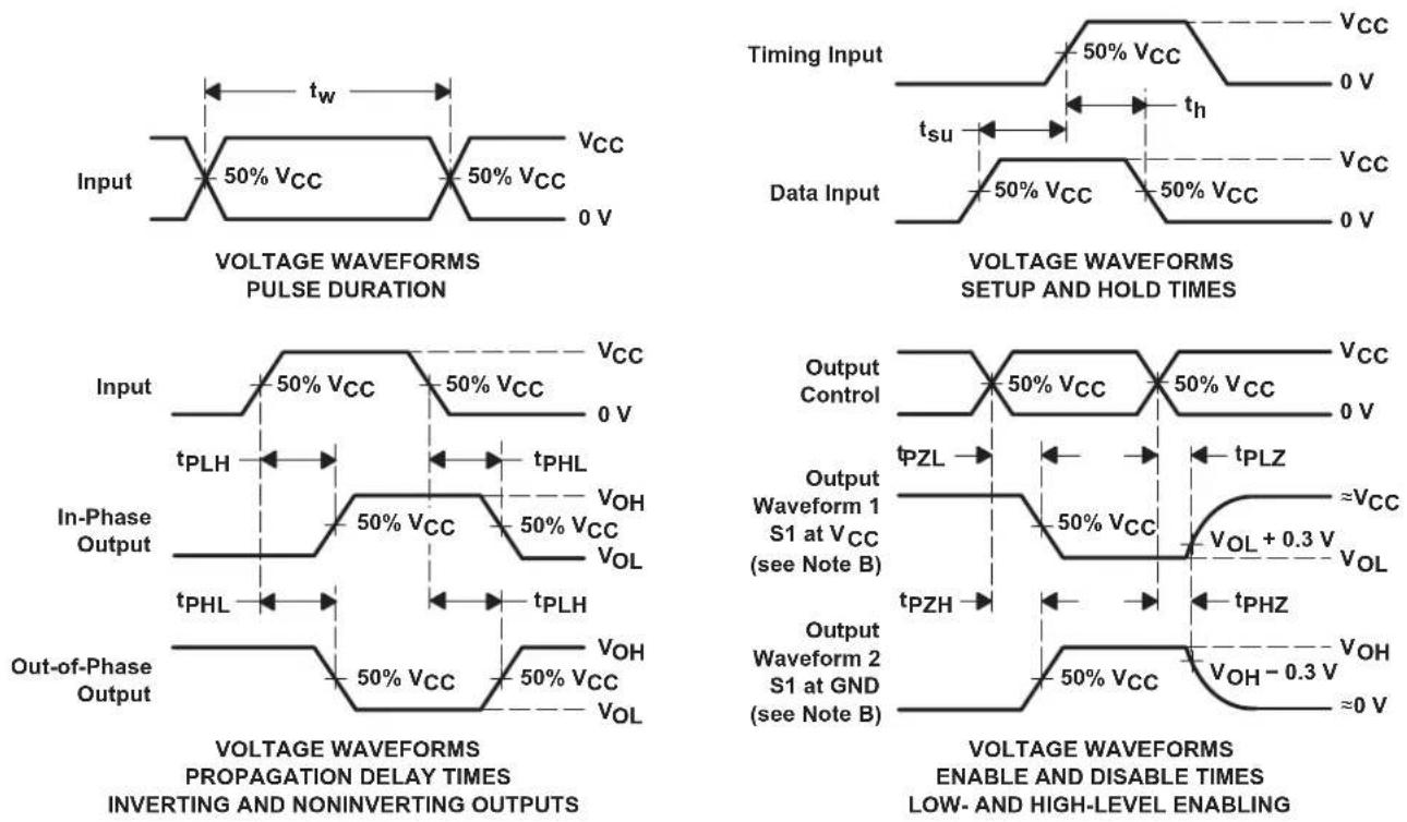
NOTES: A. C L includes probe and jig capacitance.
B. Waveform 1 is for an output with internal conditions such that the output is low except when disabled by the output control. Waveform 2 is for an output with internal conditions such that the output is high except when disabled by the output control.
C. All input pulses are supplied by generators having the following characteristics: PRR ≤ 1 MHz, Z_O = 50 , t_r ≤ 3 ns , t_f ≤ 3 ns .
D. The outputs are measured one at a time with one input transition per measurement.
E. All parameters and waveforms are not applicable to all devices.
Figure3.LoadCircuitandVoltageWaveforms
9DetailedDescription
9.1 Overview
TheSN74AHC1G125deviceisasinglebusbuffergate/linedriverwith3-stateoutput. Theoutputisdisabled whentheoutput-enable(OE)inputishigh.WhenOEislow,truedataispassedfromtheAinputtotheYoutput.
Toensurethehigh-impedancestateduringpoweruporpowerdown,OEshouldbetiedtoV cc throughapullup resistor;theminimumvalueoftheresistorisdeterminedbythecurrent-sinkingcapabilityofthedriver.
9.2 FunctionalBlockDiagram

text_image
OE A YFigure4.LogicDiagram(PositiveLogic)
9.3FeatureDescription
•Wideoperatingvoltagerange
-Operatesfrom2Vto5.5V
- Allowsdown-voltagetranslation
-Inputsacceptvoltagesto5.5V
9.4DeviceFunctionalModes
Table1.FunctionTable
| INPUTS | OUTPUTY | |
| A | ||
| LHH | ||
| L | L | L |
| H | X | Z |
10ApplicationandImplementation
NOTE
InformationinthefollowingapplicationssectionsisnotpartoftheTlcomponent specification,andTldoesnotwarrantitsaccuracyorcompleteness.TI'scustomersare responsiblefordeterminingsuitabilityofcomponentsfortheirpurposes.Customersshould validateandtesttheirdesignimplementationtoconfirmsystemfunctionality.
10.1 Application Information
SN74AHC1G125isalow-driveCMOSdevicethatcanbeusedforamultitudeofbusinterfacetypeapplications whereoutputringingisaconcern. Thelowdriveandslowedgerateswillminimizeovershootandundershooton theoutputs. Theinputscanacceptvoltagesto5.5VatanyvalidV CC makingitIdealfordowntranslation.
10.2 Typical Application

flowchart
graph TD
    A["5-V system"] --> B["μC or System Logic"]
    B --> C["A"]
    C --> D["Vcc OE"]
    D --> E["μC System Logic LEDs"]
    E --> F["5-V regulated"]
    F --> C
    C --> G["Y"]
    G --> H["GND"]
    H --> I["Ground"]
Figure5.TypicalApplicationSchematic
10.2.1 Design Requirements
ThisdeviceusesCMOStechnologyandhasbalancedoutputdrive.Careshouldbetakentoavoidbus contentionbecauseitcandrivecurrentsthatwouldexceedmaximumlimits.Thehighdrivewillalsocreatefast edgesintolightloads,soroutingandloadconditionsshouldbeconsideredtopreventringing.
10.2.2 Detailed Design Procedure
- RecommendedInputConditions
- For rise time and fall time specifications, see t / V in the Recommended Operating Conditions table.
-ForspecifiedHighandlowlevels,seeV IH andV IL intheRecommendedOperatingConditionstable.
- RecommendOutputConditions
-Loadcurrentsshouldnotexceed25mAperoutputand50mAtotalforthepart.
-OutputsshouldnotbepulledaboveV cc.
TypicalApplication(continued)
10.2.3 ApplicationCurves
Switching Characteristics Comparison
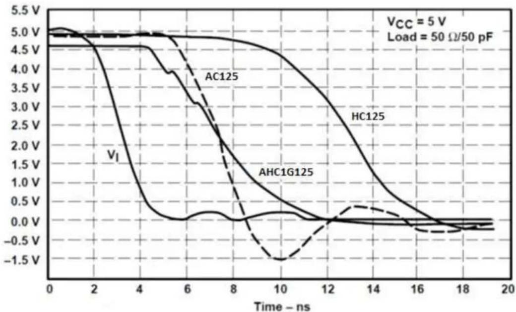
line
| Time (ns) | VI (V) | AC125 (V) | AHC1G125 (V) | HC125 (V) | |-----------|--------|-----------|--------------|-----------| | 0 | 5.0 | 5.0 | 5.0 | 5.0 | | 2 | 4.5 | 4.8 | 4.7 | 4.9 | | 4 | 0.0 | 3.5 | 3.0 | 4.8 | | 6 | -0.5 | 2.0 | 1.5 | 4.5 | | 8 | -0.2 | 0.5 | 0.0 | 3.5 | | 10 | -0.1 | -1.0 | -0.5 | 2.0 | | 12 | -0.1 | -0.5 | -0.2 | 1.0 | | 14 | -0.1 | -0.2 | -0.1 | 0.5 | | 16 | -0.1 | -0.1 | -0.1 | 0.0 | | 18 | -0.1 | -0.1 | -0.1 | -0.1 | | 20 | -0.1 | -0.1 | -0.1 | -0.1 |Figure6.
11 PowerSupplyRecommendations
ThepowersupplycanbeanyvoltagebetweentheMINandMAXsupplyvoltageratinglocatedintheRecommendedOperatingConditionstable.
EachV cc pin should have a good bypass capacitort to prevent power disturbance. For devices with a single supply, 0.1 Fis recommended. If there are multiple V cc pins, 0.01 For 0.022 Fis recommended foreach power pin. It is acceptable to parallel multiple bypass caps to reject different frequencies of noise. A 0.1 F and 1 F are commonly used in parallel. The bypass capacitor should be installed as close to the power pin as possible for best results.
12Layout
12.1 LayoutGuidelines
When using multiple bit logic devices, input should not float. In many cases, functions or part so function so digital logic devices are unused. Some examples are when only two input so at triple-input AND gate are used, or when only 3 of the 4 buffer gates are used. Such input pin should not be left unconnected because the undefined voltages at the outside connections result in undefined operational states.
Specified in Figure 7 are rules that must be observed under all circumstances. All unused inputs of digital logic devices must be connected to a high or low biastoprevent them from floating. The logic level that should be applied to any particular unused input depends on the function of the device. Generally they will be tied to GND or V_CC , whichever makes more sense or more convenient. It is acceptable to float outputs unless the part is a transceiver. If the transceiver has an output enable pin, it will disable the output section of the part when asserted. This will not disable the input section of the /Osso they also cannot float when disabled.
12.2 LayoutExample

text_image
Vcc Unused Input Input Output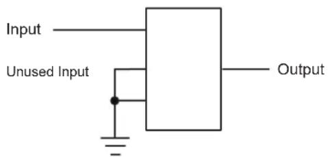
text_image
Input Unused Input OutputFigure7.LayoutDiagram
13DeviceandDocumentationSupport
13.1 Trademarks
Alltrademarksarethepropertyoftheirrespectiveowners.
13.2 Electrostatic Discharge Caution

These devices have limited built-in ESD protection. The leads should be shorted together or the device placed in conductive foam duringstorageorhandlingtopreventelectrostaticdamagetotheMOSgates.
13.3 Glossary
SLYZ022—TIGlossary.
This glossarylistsandexplainsterms,acronyms,anddefinitions.
14Mechanical, Packaging, and Orderable Information
The following pages include mechanical, packaging, and orderable information. This information is most current data available for the designated devices. This data is subject to changewithout notice and revision of this document. For browser-based versions of this datasheet, referto the left-hand navigation.
PACKAGING INFORMATION
| Orderable Device Status(1) | Package Type | Package Drawing | Pins | Package Qty | Eco Plan(2) | Lead finish/ Ball material(6) | MSL Peak Temp(3) | Op Temp (°C) | Device Marking(4-5) | Samples | |
| 74AHC1G125DBVRE4 ACTIVE SOT 23 DBV 5 3000 RoHS & Green NIPDAU Level-1-260C-UNLIM -40 to 125 A25G | Samples | ||||||||||
| 74AHC1G125DBVRG4 ACTIVE SOT-23 DBV 5 3000 RoHS & Green NIPDAU Level-1-260C-UNLIM -40 to 125 A25G | Samples | ||||||||||
| 74AHC1G125DBVTE4 ACTIVE SOT-23 DBV 5 250 RoHS & Green NIPDAU Level-1-260C-UNLIM -40 to 125 A25G | Samples | ||||||||||
| 74AHC1G125DBVTG4 ACTIVE SOT-23 DBV 5 250 RoHS & Green NIPDAU Level-1-260C-UNLIM -40 to 125 A25G | Samples | ||||||||||
| 74AHC1G125DCKRE4 | ACTIVE | SC70 | DCK | 5 | 3000 | RoHS & Green | NIPDAU | Level-1-260C-UNLIM | -40 to 125 | AM3 | Samples |
| 74AHC1G125DCKTE4 | ACTIVE | SC70 | DCK | 5 | 250 | RoHS & Green | NIPDAU | Level-1-260C-UNLIM | -40 to 125 | AM3 | Samples |
| 74AHC1G125DCKTG4 | ACTIVE | SC70 | DCK | 5 | 250 | RoHS & Green | NIPDAU | Level-1-260C-UNLIM | -40 to 125 | AM3 | Samples |
| SN74AHC1G125DBVR | ACTIVE | SOT-23 | DBV | 5 | 3000 | RoHS & Green | NIPDAU | SN | Level-1-260C-UNLIM | -40 to 125 | (A253, A25G, A25J, A25L, A25S) | Samples |
| SN74AHC1G125DBVT | ACTIVE | SOT-23 | DBV | 5 | 250 | RoHS & Green | NIPDAU | SN | Level-1-260C-UNLIM | -40 to 125 | (A253, A25G, A25J, A25L, A25S) | Samples |
| SN74AHC1G125DCK3 | ACTIVE | SC70 | DCK | 5 | 3000 | RoHS & Non-Green | SNBI | Level-1-260C-UNLIM | -40 to 85 | AMY | Samples |
| SN74AHC1G125DCKR | ACTIVE | SC70 | DCK | 5 | 3000 | RoHS & Green | NIPDAU | SN | Level-1-260C-UNLIM | -40 to 125 | (AM3, AMG, AMJ, AM L, AMS) | Samples |
| SN74AHC1G125DCKT | ACTIVE | SC70 | DCK | 5 | 250 | RoHS & Green | NIPDAU | SN | Level-1-260C-UNLIM | -40 to 125 | (AM3, AMG, AMJ, AM L, AMS) | Samples |
| SN74AHC1G125DRLR | ACTIVE | SOT-5X3 | DRL | 5 | 4000 | RoHS & Green | NIPDAUAG | Level-1-260C-UNLIM | -40 to 125 | AMS | Samples |
(1) The marketing status values are defined as follows:
ACTIVE: Product device recommended for new designs.
LIFEBUY: TI has announced that the device will be discontinued, and a lifetime-buy period is in effect.
NRND: Not recommended for new designs. Device is in production to support existing customers, but TI does not recommend using this part in a new design.
PREVIEW: Device has been announced but is not in production. Samples may or may not be available.
OBSOLETE: TI has discontinued the production of the device.
(2) RoHS: TI defines "RoHS" to mean semiconductor products that are compliant with the current EU RoHS requirements for all 10 RoHS substances, including the requirement that RoHS substance do not exceed 0.1% by weight in homogeneous materials. Where designed to be soldered at high temperatures, "RoHS" products are suitable for use in specified lead-free processes. TI may reference these types of products as "Pb-Free".

TEXAS INSTRUMENTS
www.ti.com
PACKAGE OPTION ADDENDUM
10-Dec-2020
RoHS Exempt: TI defines "RoHS Exempt" to mean products that contain lead but are compliant with EU RoHS pursuant to a specific EU RoHS exemption.
Green: TI defines "Green" to mean the content of Chlorine (Cl) and Bromine (Br) based flame retardants meet JS709B low halogen requirements of <=1000ppm threshold. Antimony trioxide based flame retardants must also meet the <=1000ppm threshold requirement.
(3) MSL, Peak Temp. - The Moisture Sensitivity Level rating according to the JEDEC industry standard classifications, and peak solder temperature.
(4) There may be additional marking, which relates to the logo, the lot trace code information, or the environmental category on the device.
(5) Multiple Device Markings will be inside parentheses. Only one Device Marking contained in parentheses and separated by a "-" will appear on a device. If a line is indented then it is a continuation of the previous line and the two combined represent the entire Device Marking for that device.
(6) Lead finish/Ball material - Orderable Devices may have multiple material finish options. Finish options are separated by a vertical ruled line. Lead finish/Ball material values may wrap to two lines if the finish value exceeds the maximum column width.
Important Information and Disclaimer: The information provided on this page represents TI's knowledge and belief as of the date that it is provided. TI bases its knowledge and belief on information provided by third parties, and makes no representation or warranty as to the accuracy of such information. Efforts are underway to better integrate information from third parties. TI has taken and continues to take reasonable steps to provide representative and accurate information but may not have conducted destructive testing or chemical analysis on incoming materials and chemicals. TI and TI suppliers consider certain information to be proprietary, and thus CAS numbers and other limited information may not be available for release.
In no event shall TI's liability arising out of such information exceed the total purchase price of the TI part(s) at issue in this document sold by TI to Customer on an annual basis.
TAPE AND REEL INFORMATION

*All dimensions are nominal
| Device Package | Type | Package Drawing | Pins | SPQ Reel | Diameter (mm) | Reel Width W1 (mm) | A0 (mm) | B0 (mm) | K0 (mm) | P1 (mm) | W (mm) | Pin1 Quadrant |
| 74AHC1G125DBVRG4 S | OT-23 DBV 5 3000 | 78.0 9.0 3.23 3.17 | 1.37 4.0 | 8.0 Q3 | ||||||||
| 74AHC1G125DBVTG4 S | OT-23 DBV 5 250 17 | 8.0 9.0 3.23 3.17 | 1.37 4.0 | 8.0 Q3 | ||||||||
| 74AHC1G125DCKTG4 S | C70 DCK 5 250 178 | 0 9.2 2.4 2.4 1.22 | 4.0 8.0 | Q3 | ||||||||
| SN74AHC1G125DBVR S | OT-23 DBV 5 3000 | 78.0 9.2 3.3 | 3.23 1.55 | 4.0 8.0 | Q3 | |||||||
| SN74AHC1G125DBVR | SOT-23 DBV | 5 | 3000 | 178.0 | 9.0 | 3.3 | 3.2 | 1.4 | 4.0 | 8.0 | Q3 | |
| SN74AHC1G125DBVR S | OT-23 DBV 5 3000 | 78.0 9.0 3.23 3.17 | 1.37 4.0 | 8.0 | Q3 | |||||||
| SN74AHC1G125DBVR S | OT-23 DBV 5 3000 | 80.0 8.4 3.23 3.17 | 1.37 4.0 | 8.0 | Q3 | |||||||
| SN74AHC1G125DBVT S | OT-23 DBV 5 250 17 | 8.0 9.0 3.23 3.17 | 1.37 4.0 | 8.0 | Q3 | |||||||
| SN74AHC1G125DBVT S | OT-23 DBV 5 250 17 | 8.0 9.0 3.3 3.2 | 1.4 4.0 | 8.0 | Q3 | |||||||
| SN74AHC1G125DBVT S | OT-23 DBV 5 250 17 | 8.0 9.2 3.3 3.23 | 1.55 4.0 | 8.0 | Q3 | |||||||
| SN74AHC1G125DBVT S | OT-23 DBV 5 250 18 | 0.0 8.4 3.23 3.17 | 1.37 4.0 | 8.0 | Q3 | |||||||
| SN74AHC1G125DCKR | SC70 DCK | 5 | 3000 | 178.0 | 9.0 | 2.4 | 2.5 | 1.2 | 4.0 | 8.0 | Q3 | |
| SN74AHC1G125DCKR SC70 DCK | 5 3000 | 0 178.0 | 9.2 2.4 2.4 | 1.22 4.0 | 8.0 | Q3 | ||||||
| SN74AHC1G125DCKR | SC70 DCK | 5 | 3000 | 180.0 | 8.4 | 2.47 | 2.3 | 1.25 | 4.0 | 8.0 | Q3 | |
| SN74AHC1G125DCKT | SC70 DCK | 5 | 250 | 178.0 | 9.0 | 2.4 | 2.5 | 1.2 | 4.0 | 8.0 | Q3 | |
| SN74AHC1G125DCKT | SC70 DCK 5 250 | 178.0 9.2 2.4 2.4 | 1.22 4.0 | 8.0 | Q3 | |||||||
| SN74AHC1G125DRLR | SOT-5X3 DRL | 5 | 4000 | 180.0 | 8.4 | 1.98 | 1.78 | 0.69 | 4.0 | 8.0 | Q3 |

text_image
TAPE AND REEL BOX DIMENSIONS W L*All dimensions are nominal
| Device | Package Type | Package Drawing | Pins | SPQ | Length (mm) | Width (mm) | Height (mm) |
| 74AHC1G125DBVRG4 SOT-23 DBV 5 3000 | 180.0 180.0 18.0 | ||||||
| 74AHC1G125DBVTG4 SOT-23 DBV 5 250 180.0 180.0 18.0 | |||||||
| 74AHC1G125DCKTG4 | SC70 | DCK 5 250 180.0 180.0 18.0 | |||||
| SN74AHC1G125DBVR SOT-23 DBV 5 3000 | 180.0 180.0 18.0 | ||||||
| SN74AHC1G125DBVR SOT-23 DBV 5 3000 | 180.0 180.0 18.0 | ||||||
| SN74AHC1G125DBVR SOT-23 DBV 5 3000 | 180.0 180.0 28.0 | ||||||
| SN74AHC1G125DBVT SOT-23 DBV 5 250 180.0 180.0 18.0 | |||||||
| SN74AHC1G125DBVT SOT-23 DBV 5 250 180.0 180.0 18.0 | |||||||
| SN74AHC1G125DBVT SOT-23 DBV 5 250 180.0 180.0 28.0 | |||||||
| SN74AHC1G125DBVT SOT-23 DBV 5 250 202.0 201.0 28.0 | |||||||
| SN74AHC1G125DCKR | SC70 | DCK 5 3000 180.0 180.0 18.0 | |||||
| SN74AHC1G125DCKR | SC70 | DCK 5 3000 180.0 180.0 18.0 | |||||
| SN74AHC1G125DCKR | SC70 | DCK 5 3000 202.0 201.0 28.0 | |||||
| SN74AHC1G125DCKT | SC70 | DCK 5 3000 5 250 180.0 180.0 18.0 | |||||
| SN74AHC1G125DCKT | SC70 | DCK 5 3000 5 250 180.0 180.0 18.0 | |||||
| SN74AHC1G125DRLR | SOT-5X3 | DRL 5 4000 202.0 201.0 28.0 |
SMALL OUTLINE TRANSISTOR
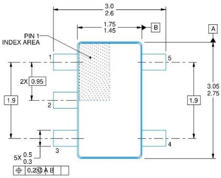
text_image
PIN 1 INDEX AREA 2X 0.95 1.9 5X 0.5 0.3 3 1.75 1.45 B 5 1.9 4 3.05 2.75 A 0.2 A B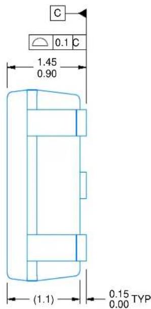
text_image
C 0.1 C 1.45 0.90 (1.1) 0.15 TYP 0.00
text_image
0.25 GAGE PLANE 8° TYP 0° 0.6 TYP 0.3 SEATING PLANE 0.22 TYP 0.084214839/F 06/2021
NOTES:
- All linear dimensions are in millimeters. Any dimensions in parenthesis are for reference only. Dimensioning and tolerancing per ASME Y14.5M.
- This drawing is subject to change without notice.
- Reference JEDEC MO-178.
- Body dimensions do not include mold flash, protrusions, or gate burrs. Mold flash, protrusions, or gate burrs shall not exceed 0.25 mm per side.
SMALL OUTLINE TRANSISTOR

text_image
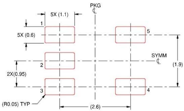
5X (1.1) PKG 1 5X (0.6) 2 2X (0.95) 3 (R0.05) TYP (2.6) SYMM (1.9)LAND PATTERN EXAMPLE
EXPOSED METAL SHOWN
SCALE:15X

text_image
SOLDER MASK OPENING METAL EXPOSED METAL 0.07 MAX ARROUNDNON SOLDER MASK
DEFINED
(PREFERRED)
text_image
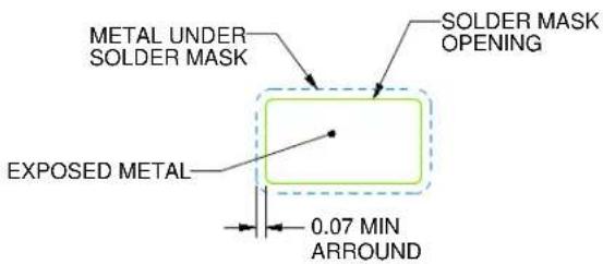
METAL UNDER SOLDER MASK SOLDER MASK OPENING EXPOSED METAL 0.07 MIN ARROUNDSOLDER MASK
DEFINED
SOLDER MASK DETAILS
4214839/F 06/2021
NOTES: (continued)
- Publication IPC-7351 may have alternate designs.
- Solder mask tolerances between and around signal pads can vary based on board fabrication site.
SMALL OUTLINE TRANSISTOR
text_image
5X (1.1) 1 5X (0.6) 2 2X(0.95) 3 (R0.05) TYP PKG 5 SYMM (1.9) (2.6)SOLDER PASTE EXAMPLE BASED ON 0.125 mm THICK STENCIL SCALE:15X
4214839/F 06/2021
NOTES: (continued)
- Laser cutting apertures with trapezoidal walls and rounded corners may offer better paste release. IPC-7525 may have alternate design recommendations.
- Board assembly site may have different recommendations for stencil design.
DCK (R-PDSO-G5)
PLASTIC SMALL-OUTLINE PACKAGE
text_image
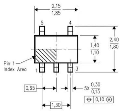
2,15 1,85 5 4 Pin 1 Index Area 1 3 2,40 1,80 1,40 1,10 0,65 5X 0,30 0,15 1,30 Φ 0,10 M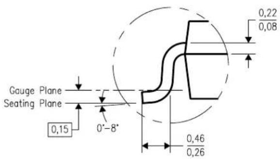
text_image
Gauge Plane Seating Plane 0,15 0°-8° 0,22 0,08 0,46 0,26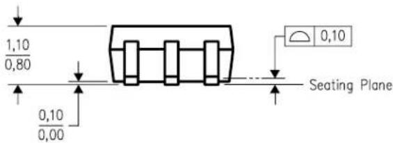
text_image
1,10 0,80 0,10 0,00 Seating Plane 0,10
4093553-3/G 01/2007
NOTES: A. All linear dimensions are in millimeters.
B. This drawing is subject to change without notice.
C. Body dimensions do not include mold flash or protrusion. Mold flash and protrusion shall not exceed 0.15 per side.
D. Falls within JEDEC MO-203 variation AA.
DCK (R-PDSO-G5)
Example Board Layout

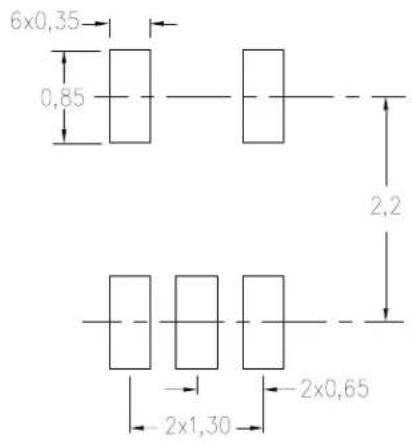
text_image
2,2 2x1,30 2x0,65 Solder Mask Opening 1,0 0,9 Pad Geometry 0,4 0,05 0,50Stencil Openings
Based on a stencil thickness of .127mm (.005inch).
text_image
6x0,35 0,85 2,2 2x1,30 2x0,654210356-2/C 07/11
NOTES: A. All linear dimensions are in millimeters.
B. This drawing is subject to change without notice.
C. Customers should place a note on the circuit board fabrication drawing not to alter the center solder mask defined pad.
D. Publication IPC-7351 is recommended for alternate designs.
E. Laser cutting apertures with trapezoidal walls and also rounding corners will offer better paste release. Customers should contact their board assembly site for stencil design recommendations. Example stencil design based on a 50% volumetric metal load solder paste. Refer to IPC-7525 for other stencil recommendations.
- All linear dimensions are in millimeters. Any dimensions in parenthesis are for reference only. Dimensioning and tolerancing per ASME Y14.5M.
- This drawing is subject to change without notice.
- This dimension does not include mold flash, protrusions, or gate burrs. Mold flash, protrusions, or gate burrs shall not exceed 0.15 mm per side.
- Reference JEDEC registration MO-293 Variation UAAD-1
text_image
5X (0.67) 1 5X (0.3) 2X (0.5) 3 (R0.05) TYP SYMM 5 SYMM 4 (1.48)LAND PATTERN EXAMPLE SCALE:30X
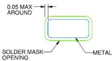
text_image
0.05 MAX AROUND SOLDER MASK OPENING METALNON SOLDER MASK DEFINED (PREFERRED)

text_image
0.05 MIN AROUND METAL UNDER SOLDER MASK SOLDER MASK OPENINGSOLDER MASK
DEFINED
SOLDERMASK DETAILS
4220753/B 12/2020
NOTES: (continued)
- Publication IPC-7351 may have alternate designs.
- Solder mask tolerances between and around signal pads can vary based on board fabrication site.
text_image
5X (0.67) 1 5X (0.3) 2X (0.5) 3 (R0.05) TYP (1.48) SYMM 5 SYMM 4 (1)SOLDER PASTE EXAMPLE BASED ON 0.1 mm THICK STENCIL SCALE:30X
4220753/B 12/2020
NOTES: (continued)
- Laser cutting apertures with trapezoidal walls and rounded corners may offer better paste release. IPC-7525 may have alternate design recommendations.
- Board assembly site may have different recommendations for stencil design.
IMPORTANT NOTICE AND DISCLAIMER
TI PROVIDES TECHNICAL AND RELIABILITY DATA (INCLUDING DATASHEETS), DESIGN RESOURCES (INCLUDING REFERENCE DESIGNS), APPLICATION OR OTHER DESIGN ADVICE, WEB TOOLS, SAFETY INFORMATION, AND OTHER RESOURCES "AS IS" AND WITH ALL FAULTS, AND DISCLAIMS ALL WARRANTIES, EXPRESS AND IMPLIED, INCLUDING WITHOUT LIMITATION ANY IMPLIED WARRANTIES OF MERCHANTABILITY, FITNESS FOR A PARTICULAR PURPOSE OR NON-INFRINGEMENT OF THIRD PARTY INTELLECTUAL PROPERTY RIGHTS.
These resources are intended for skilled developers designing with TI products. You are solely responsible for (1) selecting the appropriate TI products for your application, (2) designing, validating and testing your application, and (3) ensuring your application meets applicable standards, and any other safety, security, or other requirements. These resources are subject to change without notice. TI grants you permission to use these resources only for development of an application that uses the TI products described in the resource. Other reproduction and display of these resources is prohibited. No license is granted to any other TI intellectual property right or to any third party intellectual property right. TI disclaims responsibility for, and you will fully indemnify TI and its representatives against, any claims, damages, costs, losses, and liabilities arising out of your use of these resources.
TI's products are provided subject to TI's Terms of Sale (https:www.ti.com/legal/termsofsale.html) or other applicable terms available either on ti.com or provided in conjunction with such TI products. TI's provision of these resources does not expand or otherwise alter TI's applicable warranties or warranty disclaimers for TI products.
Mailing Address: Texas Instruments, Post Office Box 655303, Dallas, Texas 75265
Copyright © 2021, Texas Instruments Incorporated