SN74S138AN - Electronic component TEXAS INSTRUMENTS - Free user manual and instructions
Find the device manual for free SN74S138AN TEXAS INSTRUMENTS in PDF.

User questions about SN74S138AN TEXAS INSTRUMENTS
0 question about this device. Answer the ones you know or ask your own.
Ask a new question about this device
Download the instructions for your Electronic component in PDF format for free! Find your manual SN74S138AN - TEXAS INSTRUMENTS and take your electronic device back in hand. On this page are published all the documents necessary for the use of your device. SN74S138AN by TEXAS INSTRUMENTS.
USER MANUAL SN74S138AN TEXAS INSTRUMENTS
- Designed Specifically for High-Speed: Memory Decoders Data Transmission Systems
- 3 Enable Inputs to Simplify Cascading and/or Data Reception
● Schottky-Clamped for High Performance
description
These Schottky-clamped TTL MSI circuits are designed to be used in high-performance memory decoding or data-routing applications requiring very short propagation delay times. In high-performance memory systems, these decoders can be used to minimize the effects of system decoding. When employed with high-speed memories utilizing a fast enable circuit, the delay times of these decoders and the enable time of the memory are usually less than the typical access time of the memory. This means that the effective system delay introduced by the Schottky-clamped system decoder is negligible.
The 'LS138, SN54S138, and SN74S138A decode one of eight lines dependent on the conditions at the three binary select inputs and the three enable inputs. Two active-low and one active-high enable inputs reduce the need for external gates or inverters when expanding. A 24-line decoder can be implemented without external inverters and a 32-line decoder requires only one inverter. An enable input can be used as a data input for demultiplexing applications.
All of these decoder/demultiplexers feature fully buffered inputs, each of which represents only one normalized load to its driving circuit. All inputs are clamped with high-performance Schottky diodes to suppress line-ringing and to simplify system design.
The SN54LS138 and SN54S138 are characterized for operation over the full military temperature range of -55^ to 125^ . The SN74LS138 and SN74S138A are characterized for operation from 0^ to 70^ .
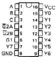
SN54LS138, SN54S138... J OR W PACKAGE SN74LS138, SN74S138A... D OR N PACKAGE
(TOP VIEW)
text_image
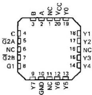
A 1 16 VCC B 2 15 Y0 C 3 14 Y1 G2A 4 13 Y2 G2B 5 12 Y3 G1 6 11 Y4 Y7 7 10 Y5 GND 8 9 Y6SN64LS138, SN54S138 . . . FK PACKAGE
(TOP VIEW)
text_image
B A NC VCC YO 3 2 1 20 19 C 4 18 Y1 G2A 5 17 Y2 NC 6 16 NC G2B 7 15 Y3 G1 8 14 Y4 9 10 11 12 13 Y7 GND NC Y6 Y5NC-No internal connection
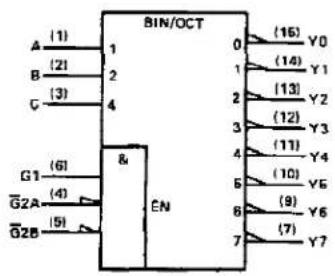
logic symbols ^†
text_image
BIN/OCT A (1) 1 B (2) 2 C (3) 4 G1 (6) 8 EN G2A (4) G2B (5) 0 (16) Y0 1 (14) Y1 2 (13) Y2 3 (12) Y3 4 (11) Y4 5 (10) Y5 6 (9) Y6 7 (7) Y7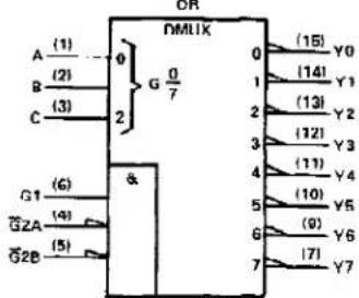
text_image
A (1) B (2) C (3) G1 (6) G2A (4) G2B (5) G G 0 G 7 DMLIK 0 (15) Y0 1 (14) Y1 2 (13) Y2 3 (12) Y3 4 (11) Y4 5 (10) Y5 6 (9) Y6 7 (7) Y7^ These symbols are in accordance with ANSI/IEEE Std 91-1984 and IEC Publication 617-12. Pin numbers shown are for D, J, N, and W packages.
logic diagram and function table
'LS138, SN54S138, SN74S138A
flowchart
graph TD
    A["ENABLE INPUTS"] --> B["G1 (6)"]
    A --> C["G2A (4)"]
    A --> D["G2B (5)"]
    B --> E["AND Gate"]
    C --> E
    D --> E
    E --> F["(15) Y0"]
    E --> G["(14) Y1"]
    E --> H["(13) Y2"]
    E --> I["(12) Y3"]
    E --> J["(11) Y4"]
    E --> K["(10) Y5"]
    L["SELECT INPUTS"] --> M["A (1)"]
    L --> N["B (2)"]
    L --> O["C (3)"]
    M --> P["NOT"]
    N --> Q["NOT"]
    O --> R["NOT"]
    P --> S["(15) Y0"]
    P --> T["(14) Y1"]
    P --> U["(13) Y2"]
    P --> V["(12) Y3"]
    P --> W["(11) Y4"]
    P --> X["(10) Y5"]
    P --> Y["(9) Y6"]
    P --> Z["(7) Y7"]
Pin numbers shown are for D, J, N, and W packages.
'LS138, SN54138, SN74S138A FUNCTION TABLE
| INPUTS | OUTPUTS | |||||||||||
| ENABLE | SELECT | |||||||||||
| G1 | 2^* | C | B | A | Y0 | Y1 | Y2 | Y3 | Y4 | Y5 | Y6 | Y7 |
| X | H | X | X | X | H | H | H | H | H | H | H | H |
| L | X | X | X | X | H | H | H | H | H | H | H | H |
| H | L | L | L | L | L | H | H | H | H | H | H | H |
| H | L | L | L | H | H | L | H | H | H | H | H | H |
| H | L | L | H | L | H | H | L | H | H | H | H | H |
| H | L | L | H | H | H | H | H | L | H | H | H | H |
| H | L | H | L | L | H | H | H | H | L | H | H | H |
| H | L | H | L | H | H | H | H | H | H | L | H | H |
| H | L | H | H | L | H | H | H | H | H | H | L | H |
| H | L | H | H | H | H | H | H | H | H | H | H | L |
·G2 - G2A + G2B
H = high level, L = low level, X = irrelevant
schematics of inputs and outputs

text_image
EQUIVALENT OF EACH ENABLE INPUT OF 'LS138 VCC 20 kΩ NOM INPUT EQUIVALENT OF EACH SELECT INPUT OF 'LS138 VCC 5 kΩ NOM INPUT TYPICAL OF OUTPUTS OF 'LS138 VCC 120 Ω NOM OUTPUT
text_image
EQUIVALENT OF EACH INPUT OF SN54S138, SN74S138A VCC 2.8 kΩ NOM INPUT TYPICAL OF OUTPUTS OF SN54S138, SN74S138A VCC 50 Ω NOM OUTPUTabsolute maximum ratings over operating free-air temperature range (unless otherwise noted)
Supply voltage, VCC (see Note 1) 7 V
Input voltage 7 V
Operating free-air temperature range: SN54LS138, SN54S138 - 55°C to 125°C
SN74LS138, SN74S138A 0°C to 70°C
Storage temperature range -65°C to 150°C
NOTE 1: Voltage values are with respect to network ground terminal.
recommended operating conditions
| SN54LS138 | SN74LS138 | UNIT | ||||||
| MIN | NOM | MAX | MIN | NOM | MAX | |||
| V_CC | Supply voltage | 4.5 | 6 | 6.5 | 4.75 | 5 | 5.25 | V |
| V_IH | High-level Input voltage | 2 | 2 | V | ||||
| V_IL | Low-level input voltage | 0.7 | 0.8 | V | ||||
| I_OH | High-level output current | -0.4 | -0.4 | mA | ||||
| I_OL | Low-level output current | 4 | 8 | mA | ||||
| T_A | Operating free-air temperature | -55 | 125 | 0 | 70 | °C | ||
electrical characteristics over recommended operating free-air temperature range (unless otherwise noted)
| PARAMETER | TEST CONDITIONS† | SN54LS138 | SN74LS138 | UNIT | |||||
| MIN | TYP‡ | MAX | MIN | TYP‡ | MAX | ||||
| V_IK | V_CC = MIN, I_I = -18 mA | -1.5 | -1.5 | V | |||||
| V_OH | V_CC = MIN, V_IH = 2 V, V_IL = MAX, I_OH = -0.4 mA | 2.5 | 3.4 | 2.7 | 3.4 | V | |||
| V_OL | V_CC = MIN, V_IH = 2 V, V_IL = MAX | I_OL = 4 mA | 0.25 | 0.4 | 0.25 | 0.4 | V | ||
| I_OL = 8 mA | 0.35 | 0.5 | |||||||
| I_I | V_CC = MAX, V_I = 7 V | 0.1 | 0.1 | mA | |||||
| I_IH | V_CC = MAX, V_I = 2.7 V | 20 | 20 | μA | |||||
| I_IL | V_CC = MAX, V_I = 0.4 V | Enable | -0.4 | -0.4 | mA | ||||
| , B, C | -0.2 | -0.2 | |||||||
| I_OS^ | V_CC = MAX | -20 | -100 | -20 | -100 | mA | |||
| I_CC | V_CC = MAX, Outputs enabled and open | 6.3 | 10 | 6.3 | 10 | mA | |||
^ For conditions shown as MIN or MAX, use the appropriate value specified under recommended operating conditions.
^ All typical values are at V_CC = 5 V , T_A = 25^ .
^5 Not more than one output should be shorted at a time, and duration of the short-circuit test should not exceed one second.
switching characteristics, VCC = 5 V, TA = 25°C
| PARAMETER1 | FROM(INPUT) | TO(OUTPUT) | LEVELSOF DELAY | TEST CONDITIONS | SN54LS138SN74LS138 | UNIT | ||
| MIN | TYP | MAX | ||||||
| tPLH | BinarySelect | Any | 2 | R_L = 2 k, C_L = 15 pF, See Note 2 | 11 | 20 | ns | |
| tPHL | 18 | 41 | ns | |||||
| tPLH | 3 | 21 | 27 | ns | ||||
| tPHL | 20 | 39 | ns | |||||
| tPLH | Enable | Any | 2 | 12 | 16 | ns | ||
| tPHL | 20 | 32 | ns | |||||
| tPLH | 3 | 14 | 26 | ns | ||||
| tPHL | 13 | 38 | ns | |||||
^1 tPLH = propagation delay time, low-to-high-level output
tPHL = propagation delay time, high-to-low-level output
NOTE 2: Load circuits and voltage waveforms are shown in Section 1.
absolute maximum ratings over operating free-air temperature range (unless otherwise noted)
Supply voltage, VCC (see Note 1) 7 V
Input voltage 5.5 V
Operating free-air temperature range: SN54S138 -55°C to 125°C
SN74S138A 0°C to 70°C
Storage temperature range -65°C to 150°C
NOTE 1: Voltage values are with respect to network ground terminal.
recommended operating conditions
| SN54S138 | SN74S138A | UNIT | ||||||
| MIN | NOM | MAX | MIN | NOM | MAX | |||
| V_CC | Supply voltage | 4.5 | 5 | 5.5 | 4.75 | 5 | 5.25 | V |
| V_IH | High-level input voltage | 2 | 2 | V | ||||
| V_IL | Low-level input voltage | 0.8 | 0.8 | V | ||||
| I_OH | High-level output current | -1 | -1 | mA | ||||
| I_OL | Low-level output current | 20 | 20 | mA | ||||
| I_A | Operating free-air temperature | -55 | 125 | 0 | 70 | °C | ||
electrical characteristics over recommended operating free-air temperature range (unless otherwise noted)
| PARAMETER | TEST CONDITIONS† | SN54S138SN74S138A | UNIT | |||||
| MIN | TYP‡ | MAX | ||||||
| V_IK | V_CC = MIN, I_I = -18 mA | -1.2 | V | |||||
| V_OH | V_CC = MIN, V_IH = 2 V, V_IL = 0.8 V, I_OH = 1 mA | SN54S' | 2.5 | 3.4 | V | |||
| SN74S' | 2.7 | 3.4 | ||||||
| V_OL | V_CC = MIN, V_IH = 2 V, V_IL = 0.8 V, I_OL = 20 mA | 0.5 | V | |||||
| I_I | V_CC = MAX, V_I = 5.5 V | 1 | mA | |||||
| I_IH | V_CC = MAX, V_I = 2.7 V | 50 | μA | |||||
| I_IL | V_CC = MAX, V_I = 0.5 V | -2 | mA | |||||
| I_OS^§ | V_CC = MAX | -40 | -100 | mA | ||||
| I_CC | V_CC = MAX, Outputs enabled and open | 49 | 74 | mA | ||||
^ For conditions shown as MIN or MAX, use the appropriate value specified under recommended operating conditions.
^ All typical values are at V_CC = 5 V , T_A = 25^ .
^9 Not more than one output should be shorted at a time, and duration of the short circuit test should not exceed one second.
switching characteristics, VCC = 5 V, TA = 25°C
| PARAMETER ^ | FROM(INPUT) | TO(OUTPUT) | LEVELSOF DELAY | TEST CONDITIONS | SN54S138SN74S138A | UNIT | ||
| MIN | TYP | MAX | ||||||
| tPLH | BinarySelect | Any | 2 | R_L=280Ω, C_L=15pF. See Note 2 | 4.5 | 7 | ns | |
| tPHL | 7 | 10.5 | ns | |||||
| tPLH | 3 | 7.5 | 12 | ns | ||||
| tPHL | 8 | 12 | ns | |||||
| tPLH | Enable | Any | 2 | 5 | 8 | ns | ||
| tPHL | 7 | 11 | ns | |||||
| tPLH | 3 | 7 | 11 | ns | ||||
| tPHL | 7 | 11 | ns | |||||
^† tPLH = propagation delay time, low-to-high-level output
t_PHL = propagation delay time, high-to-low-level output
NOTE 2: Load circuits and voltage waveforms are shown in Section 1.
PACKAGING INFORMATION
| Orderable Device Status(1) | Package Type Package Drawing | Pins Package Qty | Eco Plan(2) | Lead finish/ Ball material(6) | MSL Peak Temp(3) | Op Temp (°C) | Device Marking(4,5) | Samples |
| 76005012A ACTIVE LCCC FK 20 1 Non-RoHS | & Green | SNPB N / A for Pkg Type -55 to 125 76005012A | SNJ54LS138FK | Samples | ||||
| 7600501EA ACTIVE CDIP J 16 1 Non-RoHS | & Green | SNPB N / A for Pkg Type -55 to 125 7600501EA | SNJ54LS138J | Samples | ||||
| 7600501EA ACTIVE CDIP J 16 1 Non-RoHS | & Green | SNPB N / A for Pkg Type -55 to 125 7600501EA | SNJ54LS138J | Samples | ||||
| 7600501FA ACTIVE CFP W 16 1 Non-RoHS | & Green | SNPB N / A for Pkg Type -55 to 125 7600501FA | SNJ54LS138W | Samples | ||||
| 7600501FA ACTIVE CFP W 16 1 Non-RoHS | & Green | SNPB N / A for Pkg Type -55 to 125 7600501FA | SNJ54LS138W | Samples | ||||
| 7604101EA ACTIVE CDIP J 16 1 Non-RoHS | & Green | SNPB N / A for Pkg Type -55 to 125 7604101EA | SNJ54S138J | Samples | ||||
| 7604101EA ACTIVE CDIP J 16 1 Non-RoHS | & Green | SNPB N / A for Pkg Type -55 to 125 7604101EA | SNJ54S138J | Samples | ||||
| 7604101FA ACTIVE CFP W 16 1 Non-RoHS | & Green | SNPB N / A for Pkg Type -55 to 125 7604101FA | SNJ54S138W | Samples | ||||
| 7604101FA ACTIVE CFP W 16 1 Non-RoHS | & Green | SNPB N / A for Pkg Type -55 to 125 7604101FA | SNJ54S138W | Samples | ||||
| JM38510/07701BEA | ACTIVE CDIP J 16 1 Non-RoHS | & Green | SNPB N / A for Pkg Type -55 to 125 JM38510/ | 07701BEA | Samples | |||
| JM38510/07701BEA | ACTIVE CDIP J 16 1 Non-RoHS | & Green | SNPB N / A for Pkg Type -55 to 125 JM38510/ | 07701BEA | Samples | |||
| JM38510/07701BFA | ACTIVE CFP W 16 1 Non-RoHS | & Green | SNPB N / A for Pkg Type -55 to 125 JM38510/ | 07701BFA | Samples | |||
| JM38510/07701BFA | ACTIVE CFP W 16 1 Non-RoHS | & Green | SNPB N / A for Pkg Type -55 to 125 JM38510/ | 07701BFA | Samples | |||
| JM38510/30701B2A ACTIVE LCCC FK 20 1 Non-RoHS | & Green | SNPB N / A for Pkg Type -55 to 125 JM38510/ | 30701B2A | Samples | ||||
| JM38510/30701B2A ACTIVE LCCC FK 20 1 Non-RoHS | & Green | SNPB N / A for Pkg Type -55 to 125 JM38510/ | 30701B2A | Samples | ||||
| JM38510/30701BEA | ACTIVE CDIP J 16 1 Non-RoHS | & Green | SNPB N / A for Pkg Type -55 to 125 JM38510/ | 30701BEA | Samples | |||
Addendum-Page 1
| Orderable Device Status(1) | Package Type | Package Drawing | Pins | Package Qty | Eco Plan(2) | Lead finish/ Ball material(6) | MSL Peak Temp(3) | Op Temp (°C) | Device Marking(4-5) | Samples | |
| JM38510/30701BEA ACTIVE CDIP J 16 1 Non-RoHS | & Green | SNPB N / A for Pkg Type -55 to 125 JM38510/ | 30701BEA | Samples | |||||||
| JM38510/30701BFA ACTIVE CFP W 16 1 Non-RoHS | & Green | SNPB N / A for Pkg Type -55 to 125 JM38510/ | 30701BFA | Samples | |||||||
| JM38510/30701BFA ACTIVE CFP W 16 1 Non-RoHS | & Green | SNPB N / A for Pkg Type -55 to 125 JM38510/ | 30701BFA | Samples | |||||||
| JM38510/30701SEA ACTIVE CDIP J 16 1 Non-RoHS | & Green | SNPB N / A for Pkg Type -55 to 125 JM38510/ | 30701SEA | Samples | |||||||
| JM38510/30701SEA ACTIVE CDIP J 16 1 Non-RoHS | & Green | SNPB N / A for Pkg Type -55 to 125 JM38510/ | 30701SEA | Samples | |||||||
| JM38510/30701SFA ACTIVE CFP W 16 1 Non-RoHS | & Green | SNPB N / A for Pkg Type -55 to 125 JM38510/ | 30701SFA | Samples | |||||||
| JM38510/30701SFA ACTIVE CFP W 16 1 Non-RoHS | & Green | SNPB N / A for Pkg Type -55 to 125 JM38510/ | 30701SFA | Samples | |||||||
| M38510/07701BEA ACTIVE CDIP J 16 1 Non-RoHS | & Green | SNPB N / A for Pkg Type -55 to 125 JM38510/ | 07701BEA | Samples | |||||||
| M38510/07701BEA ACTIVE CDIP J 16 1 Non-RoHS | & Green | SNPB N / A for Pkg Type -55 to 125 JM38510/ | 07701BEA | Samples | |||||||
| M38510/07701BFA ACTIVE CFP W 16 1 Non-RoHS | & Green | SNPB N / A for Pkg Type -55 to 125 JM38510/ | 07701BFA | Samples | |||||||
| M38510/07701BFA ACTIVE CFP W 16 1 Non-RoHS | & Green | SNPB N / A for Pkg Type -55 to 125 JM38510/ | 07701BFA | Samples | |||||||
| M38510/30701B2A ACTIVE LCCC FK | 20 1 Non-RoHS | & Green | SNPB N / A for Pkg Type -55 to 125 JM38510/ | 30701B2A | Samples | ||||||
| M38510/30701B2A ACTIVE LCCC FK | 20 1 Non-RoHS | & Green | SNPB N / A for Pkg Type -55 to 125 JM38510/ | 30701B2A | Samples | ||||||
| M38510/30701BEA ACTIVE CDIP J 16 1 Non-RoHS | & Green | SNPB N / A for Pkg Type -55 to 125 JM38510/ | 30701BEA | Samples | |||||||
| M38510/30701BEA ACTIVE CDIP J 16 1 Non-RoHS | & Green | SNPB N / A for Pkg Type -55 to 125 JM38510/ | 30701BEA | Samples | |||||||
| M38510/30701BFA ACTIVE CFP W 16 1 Non-RoHS | & Green | SNPB N / A for Pkg Type -55 to 125 JM38510/ | 30701BFA | Samples | |||||||
| M38510/30701BFA ACTIVE CFP W 16 1 Non-RoHS | & Green | SNPB N / A for Pkg Type -55 to 125 JM38510/ | 30701BFA | Samples | |||||||
| M38510/30701SEA ACTIVE CDIP J 16 1 Non-RoHS | & Green | SNPB N / A for Pkg Type -55 to 125 JM38510/ | 30701SEA | Samples | |||||||
| M38510/30701SEA ACTIVE CDIP J 16 1 Non-RoHS | & Green | SNPB N / A for Pkg Type -55 to 125 JM38510/ | 30701SEA | Samples | |||||||
| M38510/30701SFA ACTIVE CFP W 16 1 Non-RoHS | & Green | SNPB N / A for Pkg Type -55 to 125 JM38510/ | 30701SFA | Samples | |||||||
| M38510/30701SFA ACTIVE CFP W 16 1 Non-RoHS | & Green | SNPB N / A for Pkg Type -55 to 125 JM38510/ | 30701SFA | Samples | |||||||
| SN54LS138J ACTIVE CDIP J 16 1 Non-RoHS | & Green | SNPB N / A for Pkg Type -55 to 125 SN54LS138J | Samples | ||||||||
| SN54LS138J ACTIVE CDIP J 16 1 Non-RoHS | & Green | SNPB N / A for Pkg Type -55 to 125 SN54LS138J | Samples | ||||||||
| SN54S138J ACTIVE CDIP J 16 1 Non-RoHS | & Green | SNPB N / A for Pkg Type -55 to 125 SN54S138J | Samples | ||||||||
| SN54S138J ACTIVE CDIP J 16 1 Non-RoHS | & Green | SNPB N / A for Pkg Type -55 to 125 SN54S138J | Samples | ||||||||
| SN74LS138D | ACTIVE | SOIC | D | 16 | 40 | RoHS & Green | NIPDAU | Level-1-260C-UNLIM | 0 to 70 | LS138 | Samples |
| SN74LS138D | ACTIVE | SOIC | D | 16 | 40 | RoHS & Green | NIPDAU | Level-1-260C-UNLIM | 0 to 70 | LS138 | Samples |
| SN74LS138DG4 | ACTIVE | SOIC | D | 16 | 40 | RoHS & Green | NIPDAU | Level-1-260C-UNLIM | 0 to 70 | LS138 | Samples |
| SN74LS138DG4 | ACTIVE | SOIC | D | 16 | 40 | RoHS & Green | NIPDAU | Level-1-260C-UNLIM | 0 t o 70 | LS138 | Samples |
| SN74LS138DR | ACTIVE | SOIC | D | 16 | 2500 | RoHS & Green | NIPDAU | Level-1-260C-UNLIM | 0 to 70 | LS138 | Samples |
| SN74LS138DR | ACTIVE | SOIC | D | 16 | 2500 | RoHS & Green | NIPDAU | Level-1-260C-UNLIM | 0 to 70 | LS138 | Samples |
| SN74LS138N | ACTIVE | PDIP | N | 16 | 25 | RoHS & Green | NIPDAU | N / A for Pkg Type | 0 to 70 | SN74LS138N | Samples |
| SN74LS138N | ACTIVE | PDIP | N | 16 | 25 | RoHS & Green | NIPDAU | N / A for Pkg Type | 0 to 70 | SN74LS138N | Samples |
| SN74LS138NE4 | ACTIVE | PDIP | N | 16 | 25 | RoHS & Green | NIPDAU | N / A for Pkg Type | 0 to 70 | SN74LS138N | Samples |
| SN74LS138NE4 | ACTIVE | PDIP | N | 16 | 25 | RoHS & Green | NIPDAU | N / A for Pkg Type | 0 to 70 | SNT4LS138N | Samples |
| SN74LS138NSR | ACTIVE | SO | NS | 16 | 2000 | RoHS & Green | NIPDAU | Level-1-260C-UNLIM | 0 to 70 | 74LS138 | Samples |
| Orderable Device Status(1) | Package Type | Package Drawing | Pins | Package Qty | Eco Plan(2) | Lead finish/ Ball material(6) | MSL Peak Temp(3) | Op Temp (°C) | Device Marking(4/5) | Samples | |
| SN74LS138NSR ACTIVE SO NS 16 2000 RoHS & Green NIPDAU Level-1-260C-UNLIM 0 to 70 74LS138 | Samples | ||||||||||
| SN74S138AD ACTIVE SOIC D 16 40 RoHS & Green NIPDAU Level-1-260C-UNLIM 0 to 70 S138A | Samples | ||||||||||
| SN74S138AN | ACTIVE | PDIP | N | 16 | 25 | RoHS & Green | NIPDAU | N / A for Pkg Type | 0 to 70 | SN74S138AN | Samples |
| SN74S138ANE4 | ACTIVE | PDIP | N | 16 | 25 | RoHS & Green | NIPDAU | N / A for Pkg Type | 0 to 70 | SN74S138AN | Samples |
| SNJ54LS138FK | ACTIVE | LCCC | FK | 20 | 1 | Non-RoHS & Green | SNPB N / A for Pkg Type | -55 to 125 | 76005012ASNJ54LS138FK | Samples | |
| SNJ54LS138FK | ACTIVE | LCCC | FK | 20 | 1 | Non-RoHS & Green | SNPB N / A for Pkg Type | -55 to 125 | 76005012ASNJ54LS138FK | Samples | |
| SNJ54LS138J | ACTIVE CDIP J 16 1 | Non-RoHS | & Green | SNPB N / A for Pkg Type | -55 to 125 | 7600501EASNJ54LS138J | Samples | ||||
| SNJ54LS138J | ACTIVE CDIP J 16 1 | Non-RoHS | & Green | SNPB N / A for Pkg Type | -55 to 125 | 7600501EASNJ54LS138J | Samples | ||||
| SNJ54LS138W | ACTIVE | CFP | W | 16 | 1 | Non-RoHS & Green | SNPB N / A for Pkg Type | -55 to 125 | 7600501FASNJ54LS138W | Samples | |
| SNJ54LS138W | ACTIVE | CFP | W | 16 | 1 | Non-RoHS & Green | SNPB N / A for Pkg Type | -55 to 125 | 7600501FASNJ54LS138W | Samples | |
| SNJ54S138J | ACTIVE CDIP J 16 1 | Non-RoHS | & Green | SNPB N / A for Pkg Type | -55 to 125 | 7604101EASNJ54S138J | Samples | ||||
| SNJ54S138J | ACTIVE CDIP J 16 1 | Non-RoHS | & Green | SNPB N / A for Pkg Type | -55 to 125 | 7604101EASNJ54S138J | Samples | ||||
| SNJ54S138W | ACTIVE | CFP | W | 16 | 1 | Non-RoHS & Green | SNPB N / A for Pkg Type | -55 to 125 | 7604101FASNJ54S138W | Samples | |
| SNJ54S138W | ACTIVE | CFP | W | 16 | 1 | Non-RoHS & Green | SNPB N / A for Pkg Type | -55 to 125 | 7604101FASNJ54S138W | Samples | |
(1) The marketing status values are defined as follows:
ACTIVE: Product device recommended for new designs.
LIFEBUY: TI has announced that the device will be discontinued, and a lifetime-buy period is in effect.
NRND: Not recommended for new designs. Device is in production to support existing customers, but TI does not recommend using this part in a new design.
PREVIEW: Device has been announced but is not in production. Samples may or may not be available.
OBSOLETE: TI has discontinued the production of the device.
(2) RoHS: TI defines "RoHS" to mean semiconductor products that are compliant with the current EU RoHS requirements for all 10 RoHS substances, including the requirement that RoHS substance do not exceed 0.1% by weight in homogeneous materials. Where designed to be soldered at high temperatures, "RoHS" products are suitable for use in specified lead-free processes. TI may reference these types of products as "Pb-Free".
RoHS Exempt: TI defines "RoHS Exempt" to mean products that contain lead but are compliant with EU RoHS pursuant to a specific EU RoHS exemption.
Green: TI defines "Green" to mean the content of Chlorine (Cl) and Bromine (Br) based flame retardants meet JS709B low halogen requirements of <=1000ppm threshold. Antimony trioxide based flame retardants must also meet the <=1000ppm threshold requirement.
(3) MSL, Peak Temp. - The Moisture Sensitivity Level rating according to the JEDEC industry standard classifications, and peak solder temperature.
(4) There may be additional marking, which relates to the logo, the lot trace code information, or the environmental category on the device.
(5) Multiple Device Markings will be inside parentheses. Only one Device Marking contained in parentheses and separated by a "\~" will appear on a device. If a line is indented then it is a continuation of the previous line and the two combined represent the entire Device Marking for that device.
(6) Lead finish/Ball material - Orderable Devices may have multiple material finish options. Finish options are separated by a vertical ruled line. Lead finish/Ball material values may wrap to two lines if the finish value exceeds the maximum column width.
Important Information and Disclaimer: The information provided on this page represents TI's knowledge and belief as of the date that it is provided. TI bases its knowledge and belief on information provided by third parties, and makes no representation or warranty as to the accuracy of such information. Efforts are underway to better integrate information from third parties. TI has taken and continues to take reasonable steps to provide representative and accurate information but may not have conducted destructive testing or chemical analysis on incoming materials and chemicals. TI and TI suppliers consider certain information to be proprietary, and thus CAS numbers and other limited information may not be available for release.
In no event shall TI's liability arising out of such information exceed the total purchase price of the TI part(s) at issue in this document sold by TI to Customer on an annual basis.
OTHER QUALIFIED VERSIONS OF SN54LS138, SN54LS138-SP, SN74LS138 :
• Catalog : SN74LS138, SN54LS138
• Military : SN54LS138
• Space : SN54LS138-SP
NOTE: Qualified Version Definitions:
• Catalog - TI's standard catalog product
• Military - QML certified for Military and Defense Applications
• Space - Radiation tolerant, ceramic packaging and qualified for use in Space-based application
TAPE AND REEL INFORMATION

*All dimensions are nominal
| Device Package | Type | Package Drawing | Pins | SPQ Reel | Diameter (mm) | Reel Width W1 (mm) | A0 (mm) | B0 (mm) | K0 (mm) | P1 (mm) | W (mm) | Pin1 Quadrant |
| SN74LS138DR SOIG | D 16 2500 | 330.0 16 | 4 6.5 | 10.3 2.1 8 | 0 16.0 Q1 | |||||||
| SN74LS138NSR SO | NS 16 2000 | 330.0 16 | 4 8.2 | 10.5 2.5 12 | 2.0 16.0 Q1 |
text_image
TAPE AND REEL BOX DIMENSIONS W L*All dimensions are nominal
| Device | Package Type | Package Drawing | Pins | SPQ | Length (mm) | Width (mm) | Height (mm) |
| SN74LS138DR SOIC D | 16 2500 340.5 336.1 | 32.0 | |||||
| SN74LS138NSR SO NS | 16 2000 853.0 449.0 | 35.0 |
TUBE
text_image
T - Tube height W-Tube width L - Tube length B - Alignment groove width*All dimensions are nominal
| Device | Package Name | Package Type | Pins | SPQ | L (mm) | W (mm) | T (μm) | B (mm) |
| 76005012A FK LCC | C 20 1 506.98 12.06 | 2030 NA | ||||||
| JM38510/07701BFA W | CFP 16 1 | 506.98 26.16 62 | 20 NA | |||||
| JM38510/30701B2A FK | LCCC 20 1 506.98 | 12.06 2030 NA | ||||||
| JM38510/30701BFA W | CFP 16 1 | 506.98 26.16 62 | 20 NA | |||||
| JM38510/30701SFA W | CFP 16 1 | 506.98 26.16 62 | 20 NA | |||||
| M38510/07701BFA | W CFP | 16 1 506 | 98 26.16 62 | 20 NA | ||||
| M38510/30701B2A | FK LCCC 20 1 506.98 12.06 | 2030 NA | ||||||
| M38510/30701BFA | W CFP | 16 1 506 | 98 26.16 62 | 20 NA | ||||
| M38510/30701SFA | W CFP | 16 1 506 | 98 26.16 62 | 20 NA | ||||
| SN74LS138D | D | SOIC | 16 | 40 | 507 | 8 | 3940 | 4.32 |
| SN74LS138DG4 | D | SOIC | 16 | 40 | 507 | 8 | 3940 | 4.32 |
| SN74LS138N | N | PDIP | 16 | 25 | 506 | 13.97 | 11230 | 4.32 |
| SN74LS138N | N | PDIP | 16 | 25 | 506 | 13.97 | 11230 | 4.32 |
| SN74LS138NE4 | N | PDIP | 16 | 25 | 506 | 13.97 | 11230 | 4.32 |
| SN74LS138NE4 | N | PDIP | 16 | 25 | 506 | 13.97 | 11230 | 4.32 |
| SN74S138AD | D | SOIC | 16 | 40 | 507 | 8 | 3940 | 4.32 |
| SN74S138AN | N | PDIP | 16 | 25 | 506 | 13.97 | 11230 | 4.32 |
| SN74S138AN | N | PDIP | 16 | 25 | 506 | 13.97 | 11230 | 4.32 |
| SN74S138ANE4 | N | PDIP | 16 | 25 | 506 | 13.97 | 11230 | 4.32 |
| SN74S138ANE4 | N | PDIP | 16 | 25 | 506 | 13.97 | 11230 | 4.32 |
| SNJ54LS138FK | FK LCCC 20 1 506.98 12.06 | 2030 NA |
SOP
4220735/A 12/2021
NOTES:
- All linear dimensions are in millimeters. Dimensions in parenthesis are for reference only. Dimensioning and tolerancing per ASME Y14.5M.
- This drawing is subject to change without notice.
- This dimension does not include mold flash, protrusions, or gate burrs. Mold flash, protrusions, or gate burrs shall not exceed 0.15 mm, per side.
- This dimension does not include interlead flash. Interlead flash shall not exceed 0.25 mm, per side.
SOP
text_image
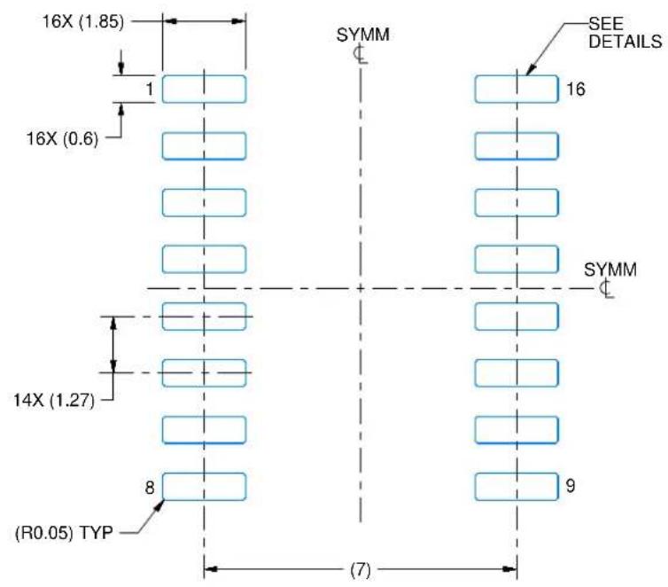
16X (1.85) 1 16X (0.6) SYMM SEE DETAILS 16 SYMM 14X (1.27) 8 (R0.05) TYP 9 (7)LAND PATTERN EXAMPLE SCALE:7X
text_image
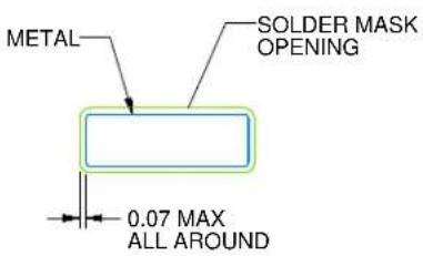
METAL SOLDER MASK OPENING 0.07 MAX ALL AROUNDNON SOLDER MASK DEFINED

text_image
SOLDER MASK OPENING METAL 0.07 MIN ALL AROUNDSOLDER MASK
DEFINED
SOLDER MASK DETAILS
4220735/A 12/2021
NOTES: (continued)
- Publication IPC-7351 may have alternate designs.
- Solder mask tolerances between and around signal pads can vary based on board fabrication site.
SOP

text_image
16X (1.85) 1 16X (0.6) 14X (1.27) 8 (R0.05) TYP SYMM 16 SYMM 9 (7)SOLDER PASTE EXAMPLE BASED ON 0.125 mm THICK STENCIL SCALE:7X
4220735/A 12/2021
NOTES: (continued)
- Laser cutting apertures with trapezoidal walls and rounded corners may offer better paste release. IPC-7525 may have alternate design recommendations.
- Board assembly site may have different recommendations for stencil design.
FK (S-CQCC-N**)
28 TERMINAL SHOWN
LEADLESS CERAMIC CHIP CARRIER

| NO. OF TERMINALS** | A | B | ||
| MIN | MAX | MIN | MAX | |
| 20 | 0.342(8,69) | 0.358(9,09) | 0.307(7,80) | 0.358(9,09) |
| 28 | 0.442(11,23) | 0.458(11,63) | 0.406(10,31) | 0.458(11,63) |
| 44 | 0.640(16,26) | 0.660(16,76) | 0.495(12,58) | 0.560(14,22) |
| 52 | 0.740(18,78) | 0.761(19,32) | 0.495(12,58) | 0.560(14,22) |
| 68 | 0.938(23,83) | 0.962(24,43) | 0.850(21,6) | 0.858(21,8) |
| 84 | 1.141(28,99) | 1.165(29,59) | 1.047(26,6) | 1.063(27,0) |
4040140/D 01/11
NOTES: A. All linear dimensions are in inches (millimeters).
B. This drawing is subject to change without notice.
C. This package can be hermetically sealed with a metal lid.
D. Falls within JEDEC MS-004
D (R-PDSO-G16)
PLASTIC SMALL OUTLINE
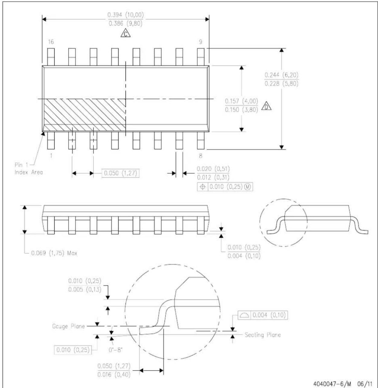
text_image
0.394 (10,00) 0.386 (9,80) 16 9 0.244 (6,20) 0.228 (5,80) 0.157 (4,00) 0.150 (3,80) Pin 1 Index Area 1 8 0.050 (1,27) 0.020 (0,51) 0.012 (0,31) ⊕ 0.010 (0,25) M 0.069 (1,75) Max 0.010 (0,25) 0.004 (0,10) Gcuge Plane 0.010 (0,25) 0.005 (0,13) 0'-8" Seating Plane 0.010 (0,25) 0.050 (1,27) 0.016 (0,40) 4040047-6/M 06/11NOTES: A. All linear dimensions are in inches (millimeters).
B. This drawing is subject to change without notice.
Body length does not include mold flash, protrusions, or gate burrs. Mold flash, protrusions, or gate burrs shall not exceed 0.006 (0,15) each side.
Body width does not include interlead flash. Interlead flash shall not exceed 0.017 (0,43) each side.
E. Reference JEDEC MS-012 variation AC.
D (R-PDSO-G16)
NOTES: A. All linear dimensions are in millimeters.
B. This drawing is subject to change without notice.
C. Publication IPC-7351 is recommended for alternate designs.
D. Laser cutting apertures with trapezoidal walls and also rounding corners will offer better paste release. Customers should contact their board assembly site for stencil design recommendations. Refer to IPC-7525 for other stencil recommendations.
E. Customers should contact their board fabrication site for solder mask tolerances between and around signal pads.
MECHANICAL DATA
NS (R-PDSO-G\*\*)
PLASTIC SMALL-OUTLINE PACKAGE
14-PINS SHOWN

text_image
1,27 14 0,51 0,35 Ø 0,25① 8 5,60 5,00 8,20 7,40 1 7 A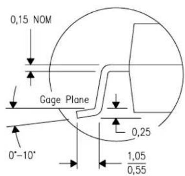
text_image
0,15 NOM Gage Plane 0,25 0°-10° 1,05 0,55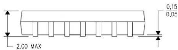
text_image
2,00 MAX 0,15 0,05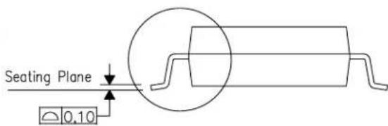
text_image
Seating Plane 0.10| DIM\PINS ** | 14 | 16 | 20 | 24 |
| A MAX | 10,50 | 10,50 | 12,90 | 15,30 |
| A MIN | 9,90 | 9,90 | 12,30 | 14,70 |
4040062/C 03/03
NOTES: A. All linear dimensions are in millimeters.
B. This drawing is subject to change without notice.
C. Body dimensions do not include mold flash or protrusion, not to exceed 0,15.
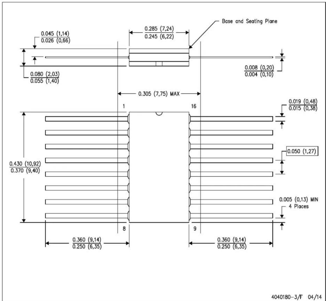
W (R-GDFP-F16)
CERAMIC DUAL FLATPACK
other
| Dimension | Value | | ----------------- | ------- | | Base and Seating Plane | 0.285 (7,24) | | Base and Seating Plane | 0.245 (6,22) | | Base and Seating Plane | 0.008 (0,20) | | Base and Seating Plane | 0.004 (0,10) | | Base and Seating Plane | 0.305 (7,75) MAX | | Base and Seating Plane | 0.360 (9,14) | | Base and Seating Plane | 0.250 (6,35) | | Base and Seating Plane | 0.430 (10,92) | | Base and Seating Plane | 0.370 (9,40) | | Base and Seating Plane | 0.45 (1,14) | | Base and Seating Plane | 0.026 (0,66) | | Base and Seating Plane | 0.080 (2,03) | | Base and Seating Plane | 0.055 (1,40) | | Base and Seating Plane | 1 | | Base and Seating Plane | 16 | | Base and Seating Plane | 8 | | Base and Seating Plane | 9 | | Base and Seating Plane | 0.360 (9,14) | | Base and Seating Plane | 0.250 (6,35) | | Base and Seating Plane | 0.360 (9,14) | | Base and Seating Plane | 0.250 (6,35) | | Base and Seating Plane | 0.360 (9,14) | | Base and Seating Plane | 1 | | Base and Seating Plane | 16 | | Base and Seating Plane | 8 | | Base and Seating Plane | 9 | | Base and Seating Plane | 16 | | Base and Seating Plane | 1 | | Base and Seating Plane | 16 | | Base and Seating Plane | 8 | | Base and Seating Plane | 9 | | Base and Seating Plane | 16 | | Base and Seating Plane | 8 | | Base and Seating Plane | 9 | | Base and Seating Plane | 16 | | Base and Seating Plane | 1 | | Base and Seating Plane | 16 | | Base and Seating Plane | 8 | | Base and Seating Plane | 9 | | Base and Seating PlaneNOTES: A. All linear dimensions are in inches (millimeters).
B. This drawing is subject to change without notice.
C. This package can be hermetically sealed with a ceramic lid using glass frit.
D. Index point is provided on cap for terminal identification only.
E. Falls within MIL STD 1835 GDFP2-F16
text_image
B 14 8 C 1 0.065 (1,65) 0.045 (1,14)| PINS **DIM | 14 | 16 | 18 | 20 |
| A | 0.300(7,62)BSC | 0.300(7,62)BSC | 0.300(7,62)BSC | 0.300(7,62)BSC |
| B MAX | 0.785(19,94) | .840(21,34) | 0.960(24,38) | 1.060(26,92) |
| B MIN | — | — | — | — |
| C MAX | 0.300(7,62) | 0.300(7,62) | 0.310(7,87) | 0.300(7,62) |
| C MIN | 0.245(6,22) | 0.245(6,22) | 0.220(5,59) | 0.245(6,22) |
text_image
0.005 (0,13) MIN 0.060 (1,52) 0.015 (0,38) 0.200 (5,08) MAX Seating Plane 0.130 (3,30) MIN 0.026 (0,66) 0.014 (0,36) 0.100 (2,54) 0.014 (0,36) 0.008 (0,20) A 0°-15°4040083/F 03/03
NOTES: A. All linear dimensions are in inches (millimeters).
B. This drawing is subject to change without notice.
C. This package is hermetically sealed with a ceramic lid using glass frit.
D. Index point is provided on cap for terminal identification only on press ceramic glass frit seal only.
E. Falls within MIL STD 1835 GDIP1-T14, GDIP1-T16, GDIP1-T18 and GDIP1-T20.
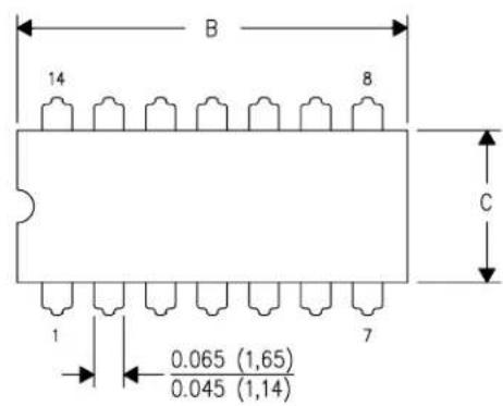
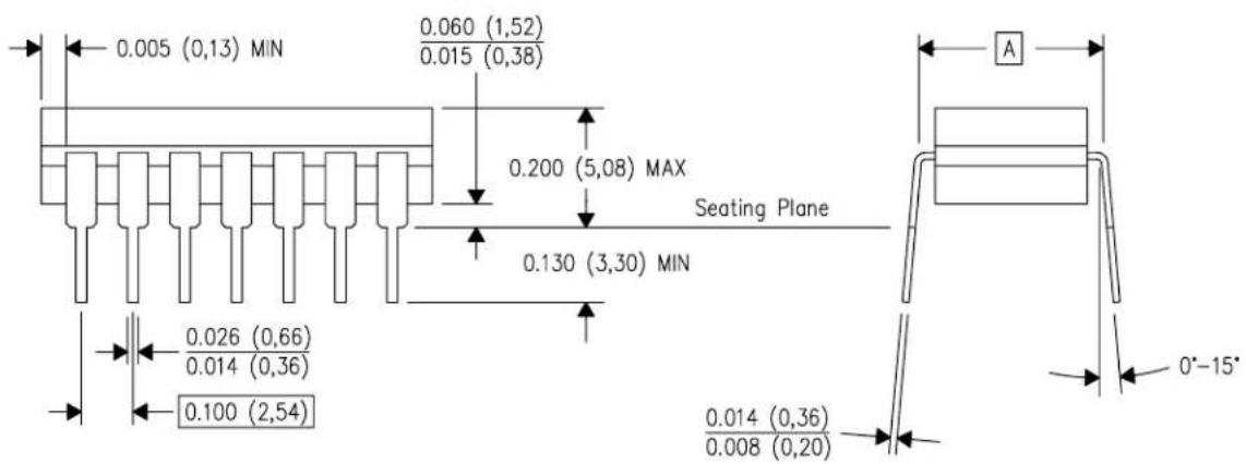
N (R-PDIP-T\*\*)
16 PINS SHOWN
PLASTIC DUAL-IN-LINE PACKAGE

text_image
A 16 9 0.260 (6,60) 0.240 (6,10) 1 8 0.070 (1,78) 0.045 (1,14)C
| DIM\PINS ** | 14 | 16 | 18 | 20 |
| A MAX | 0.775(19,69) | 0.775(19,69) | 0.920(23,37) | 1.060(26,92) |
| A MIN | 0.745(18,92) | 0.745(18,92) | 0.850(21,59) | 0.940(23,88) |
| MS-001VARIATION | AA | BB | AC | AD |
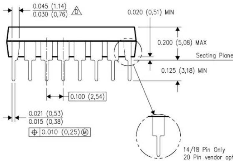
text_image
0.045 (1,14) 0.030 (0,76) D 0.020 (0,51) MIN 0.200 (5,08) MAX Seating Plane 0.125 (3,18) MIN 0.100 (2,54) 0.021 (0,53) 0.015 (0,38) ⊕ 0.010 (0,25) M 14/18 Pin Only 20 Pin vendor opt
text_image
0.325 (8,26) 0.300 (7,62) 0.015 (0,38) Gauge Plane 0.010 (0,25) NOM 0.430 (10,92) MAX4040049/E 12/2002
NOTES: A. All linear dimensions are in inches (millimeters).
B. This drawing is subject to change without notice.
C Falls within JEDEC MS-001, except 18 and 20 pin minimum body length (Dim A).
The 20 pin end lead shoulder width is a vendor option, either half or full width.
IMPORTANT NOTICE AND DISCLAIMER
TI PROVIDES TECHNICAL AND RELIABILITY DATA (INCLUDING DATA SHEETS), DESIGN RESOURCES (INCLUDING REFERENCE DESIGNS), APPLICATION OR OTHER DESIGN ADVICE, WEB TOOLS, SAFETY INFORMATION, AND OTHER RESOURCES "AS IS" AND WITH ALL FAULTS, AND DISCLAIMS ALL WARRANTIES, EXPRESS AND IMPLIED, INCLUDING WITHOUT LIMITATION ANY IMPLIED WARRANTIES OF MERCHANTABILITY, FITNESS FOR A PARTICULAR PURPOSE OR NON-INFRINGEMENT OF THIRD PARTY INTELLECTUAL PROPERTY RIGHTS.
These resources are intended for skilled developers designing with TI products. You are solely responsible for (1) selecting the appropriate TI products for your application, (2) designing, validating and testing your application, and (3) ensuring your application meets applicable standards, and any other safety, security, regulatory or other requirements.
These resources are subject to change without notice. TI grants you permission to use these resources only for development of an application that uses the TI products described in the resource. Other reproduction and display of these resources is prohibited. No license is granted to any other TI intellectual property right or to any third party intellectual property right. TI disclaims responsibility for, and you will fully indemnify TI and its representatives against, any claims, damages, costs, losses, and liabilities arising out of your use of these resources.
TI's products are provided subject to TI's Terms of Sale or other applicable terms available either on ti.com or provided in conjunction with such TI products. TI's provision of these resources does not expand or otherwise alter TI's applicable warranties or warranty disclaimers for TI products.
TI objects to and rejects any additional or different terms you may have proposed.
Mailing Address: Texas Instruments, Post Office Box 655303, Dallas, Texas 75265
Copyright © 2022, Texas Instruments Incorporated