SN74LV138ADR - Electronic component TEXAS INSTRUMENTS - Free user manual and instructions
Find the device manual for free SN74LV138ADR TEXAS INSTRUMENTS in PDF.

User questions about SN74LV138ADR TEXAS INSTRUMENTS
0 question about this device. Answer the ones you know or ask your own.
Ask a new question about this device
Download the instructions for your Electronic component in PDF format for free! Find your manual SN74LV138ADR - TEXAS INSTRUMENTS and take your electronic device back in hand. On this page are published all the documents necessary for the use of your device. SN74LV138ADR by TEXAS INSTRUMENTS.
USER MANUAL SN74LV138ADR TEXAS INSTRUMENTS
| • 2-V toCC Operation V | off Supports • I Partial-Power-DownOperation | |||||||
| • Maxpd of 9.5 ns at 5 V | ||||||||
| • TypicalOLP (Output V Ground <0.8 CC V at3 A V V25 T°C | • Lath Ube) PerformanceJESD 17 | |||||||
| • TypicalOHV (Output OH UndershooV >2.3 CC V at3 A V V25 T°C | • ESD Protection Exceeds- 2000-V Human-Body | |||||||
| • Support Mixed-ModePorts | Voltage Operation- 1000-V Charged-Device | |||||||
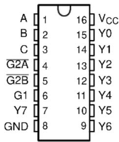
SN54LV138A ... J OR W PACKAGE
SN74LV138A ... D, DB, DGV, NS
OR PW PACKAGE
(TOP VIEW)
text_image
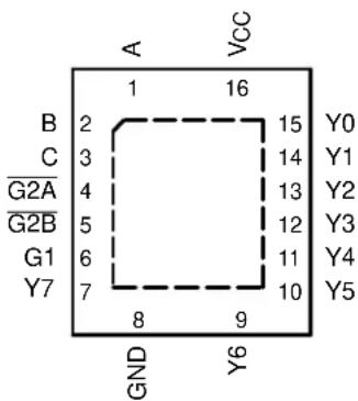
A 1 16 VCC B 2 15 Y0 C 3 14 Y1 G2A 4 13 Y2 G2B 5 12 Y3 G1 6 11 Y4 Y7 7 10 Y5 GND 8 9 Y6SN74LV138A...RGY PACKAGE
(TOP VIEW)
text_image
A VCC 1 2 3 4 5 6 7 8 9 Y0 Y1 Y2 Y3 Y4 Y5 B C G2A G2B G1 Y7 GND Y6SN54LV138A ... FK PACKAGE
(TOP VIEW)

text_image
B A NC VCC Y0 3 2 1 20 19 C 4 18 Y1 G2A 5 17 Y2 NC 6 16 NC G2B 7 15 Y3 G1 8 14 Y4 9 10 11 12 13 Y7 GND NC Y6 Y5NC - No internal connection
DESCRIPTION/ORDERING INFORMATION
| The | 'LV138A | devices | are | 3-line | to CC operation. | decoders/de |
ORDERING
| T_A | PACKAGE^(1) | ORDERABLE | PART NUMBER | |||
| -40 °C to | QFN - RGY | Reel of 1000 | SN74LV138ARGYR | |||
| SOIC - D | Tube of | 40 SN74LV138AD | LV138A | |||
| Reel of 2500 | SN74LV138ADR | |||||
| SOP - NS | Reel of 2000 | SN74LV138ANSR | ||||
| 85 °C | SSOP - | DB Reel | of 2000 | |||
| TSSOP | Tube of | 90 SN74LV138APW | SN74LV138APWR | |||
| PW | Reel of 2000 | |||||
| Reel of 250 | SN74LV138APWT | |||||
| TVSOP | DGV | Reel of 2000 | SN74LV138ADGVR | |||
| -55 °C to | CDIP - J | Tube of 25 | SNJ54LV138AJ | |||
| 125 °C | CFP - | W Tube of 150 | SNJ54LV138AW | |||
| LCCC - FK | Tube of 55 | SNJ54LV138AFK | ||||
(1) Package www.ti.com/sc/package.

UNLESS
DUCTION
ucts
standard
include
OTHERWISE
DATA
conform
[Non-Text]
W
testing
The Ground Truth image displays a single, solid horizontal line. According to Rule 2 (UNDERSCORE & LINE RULES), this is a stylistic or background line, not a placeholder underscore. Therefore, the OCR result must ignore it and output nothing or only meaningful text. The provided OCR content is "____", which consists of four underscores. This is an incorrect interpretation of the line as a placeholder, violating the rule that stylistic lines must be ignored. The OCR has hallucinated placeholder underscores where none should exist in the GT. Hence, the OCR result is inconsistent with the Ground Truth.
information
specifications
The Ground Truth image displays a single, solid horizontal line. According to Rule 2 (UNDERSCORE & LINE RULES), this is a stylistic or background line, not a placeholder underscore. Therefore, the OCR result must ignore it and output nothing or only meaningful text. The provided OCR content is "____", which consists of four underscores. This is an incorrect interpretation of the line as a placeholder, violating the rule that stylistic lines must be ignored. The OCR has hallucinated underscores where none should exist based on the GT's visual context. Hence, the OCR result is inconsistent with the Ground Truth.
of all
NOTED
ation
ns
Production
parameters.
this
current
per the
processing
document
as of
terms
Copyright
publication
of Texas
does
contains
[Non-Text]
[Non-Text]
not
©
ate
ments
ssarily
19982005.
Prod-
Te:
DESCRIPTION/ORDERING INFORMATION (CONTINUED)
| These short the delay the | devices propagation effects times memory. | are of of this | designed delay decoding decoders means that the binary-select two active-low when requires | for In When and the effective inputs (G2A, expanding. only one inverter. | high-performance high-performance employed enable system (A, ( |
| The eight external and applications. | conditions output gates a 32-line | lines. or decoder | |||
| These outputs, | devices preventing | are | fully damaged specified off. | The off current | circuitry partial-power holes backflow |
FUNCTION
TABLE
| ENABLE | INPUTS | SELECT | INPUTS | |||||||
| G1 | G2A | G2B | C | B | A | Y0 | Y1 | |||
| X | H | X | X | X | X | H | H | H | H | |
| X | X | H | X | X | X | H | H | H | H | |
| L | X | X | X | X | X | H | H | H | H | |
| H | L | L | L | L | L | L | H | H | H | |
| H | L | L | L | L | H | H | L | H | H | |
| H | L | L | L | H | L | H | H | L | H | |
| H | L | L | L | H | H | H | H | H | L | |
| H | L | L | H | L | L | H | H | H | H | |
| H | L | L | H | L | H | H | H | H | H | |
| H | L | L | H | H | L | H | H | H | H | |
| H | L | L | H | H | H | H | H | H | H | |

flowchart
graph TD
    subgraph Select Inputs
        A1["A 1"] --> AND1["NOT"]
        B2["B 2"] --> AND2["NOT"]
        C3["C 3"] --> AND3["NOT"]
    end
    subgraph Enable Inputs
        G1["G1 6"] --> AND4["NOT"]
        G2A["G2A 4"] --> AND5["NOT"]
        G2B["G2B 5"] --> AND6["NOT"]
    end
    AND1 --> OR1["OR"]
    AND2 --> OR1
    AND3 --> OR1
    AND4 --> OR2["OR"]
    AND5 --> OR2
    AND6 --> OR2
    OR1 --> D0["AND"]
    OR2 --> D0
    D0 --> Y0["Y0"]
    D0 --> Y1["Y1"]
    D0 --> Y2["Y2"]
    D0 --> Y3["Y3"]
    D0 --> Y4["Y4"]
    D0 --> Y5["Y5"]
    D0 --> Y6["Y6"]
    D0 --> Y7["Y7"]
    style Select Inputs fill:#f9f,stroke:#333
    style Enable Inputs fill:#bbf,stroke:#333
Pin numbers shown are for the D, DB, DGV, J, NS, PW, RGY, and W packages.
Absolute Maximum Ratings ^(1)
over operating free-air temperature range (unless otherwise noted)
| MIN | MAX | ||||
| V_CC | Supply voltage range | ||||
| V_I | Input voltage range | -0.5 | 7 | ||
| V_O | Voltage range applied to any (2) output in -0.5e high-impedance V | ||||
| V_O | Output voltage(3) range | -0.5 cc + 0.5 | V | ||
| I_IK | Input clamp current | I< 0 V | -20 mA | ||
| I_OK | Output clamp current | O< 0 V | -50 mA | ||
| I_O | Continuous output | current 0 to V | V ± 25 | mA | |
| Continuous CC or current AND through V | ± 50 m | ||||
| θ_JA | Package thermal impedance | D package | 73 | ||
| DB package | 82 | ||||
| DGV package | 120 | ||||
| NS package | 64 | ||||
| PW package | 108 | ||||
| RGY package | 39 | ||||
| T_stg | Storage temperature range | ||||
| (1) | Stresses | beyond | those operation | listed | under of the | "absolute device at these to absolute-maximum-rated ratings | maximum or may | be | ||
| only, conditions" | and | functional is not implied. | ||||||||
| (2) | The | input | and | output | negative-voltage | |||||
| (3) | This | value | is | limited | to 5.5 V maximum. | |||||
| (4) | The | package | thermal | impedance | is calculated | in | accordar | |||
| (5) | The | package | thermal | impedance | is calculated | in | accordar | |||
Recommended Operating Conditions ^(1)
| SN54LV138A(2) | SN74LV138A | UNIT | |||||||||
| MIN MAX MIN MAX | |||||||||||
| V_CC | Supply voltage | 2 | 5.5 | ||||||||
| V_IH | High-level input | V_CC= 2 V | 1.5 | 1.5 | 0.50-50-50×6-55 | ||||||
| V_CC= 2.3 V to 2.7 V_CC · 0.7 V_CC · 0.7 V_CC · 0.7 V_CC · 0.7 V_CC · 0.7 V_CC · 0.7 V_CC · 0.7 V_CC · 0.7 V_CC · 0.7 V_CC · 0.7 V_CC · 1.3 | \(V_CC · 0.7 V_CC · 0.7 V_CC · 0.7 V_CC · 0.7 V_CC · 0.7 V_CC · 0.7 V_CC · 0.7 V_CC · 0.7 V_CC · 0.7 V_CC · 0.7 | ||||||||||
| \(V_CC= 3 V to 3.6 V_CC · 0.7 V_CC · 0.7 V_CC · 0.7 V_CC · 0.7 V_CC · 0.7 V_CC · 0.7 V_CC · 0.7 V_CC · 0.7 V_CC · 0.7 V_CC · 0.3 | V_CC · 0.7 V_CC · 0.7 V_CC · 0.7 V_CC · 0.7 V_CC · 0.7 V_CC · 0.7 V_CC · 0.7 V_CC · 0.7 V_CC · 0.7 V_CC | ||||||||||
| V_CC= 4.5 V to 5.5 V_CC · 0.7 V_CC · 0.7 V_CC · 0.7 V_CC · 0.7 V_CC · 0.7 V_CC · 0.7 V_CC · 0.7 V_CC · 0.7 V_CC · 0.7 V_CC · 0.5 | V_CC · 0.7 V_CC · 0.7 V_CC · 0.7 V_CC · 0.7 V_CC · 0.7 V_CC · 0.7 V_CC · 0.7 V_CC · 0.7 V_CC · 0.7 V_C | ||||||||||
| V_IL | Low-level input | V_CC= 2 V | 0.5 | ||||||||
| V_CC= 2.3 V to 2.7 V_CC · 0.3 V_CC · 0.3 V_CC · 0.3 V_CC · 0.3 V_CC · 0.3 V_CC · 0.3 V_CC · 0.3 V_CC · 0.3 V_CC · 0.3 V_CC · 0.3 V_CC · 0.5 | V_CC · 0.3 V_CC · 0.3 V_CC · 0.3 V_CC · 0.3 V_CC · 0.3 V_CC · 0.3 V_CC · 0.3 V_CC · 0.3 V_CC · 0.5 | ||||||||||
| V_CC= 3 V to 3.6 V_CC · 0.3 V_CC · 0.3 V_CC · 0.3 V_CC · 0.3 V_CC · 0.3 V_CC · 0.3 V_CC · 0.3 V_CC · 0.3 V_CC · 0.3 V_CC · 0.7 | V_CC · 0.3 V_CC · 0.3 V_CC · 0.3 V_CC · 0.3 V_CC · 0.3 V_CC · 0.3 V_CC · 0.3 V_CC · 0.3 V_CC · 0.3 V_CC · 0.3 | ||||||||||
| V_I | Input voltage | 0 | |||||||||
| V_O | Output voltage | cc | 0 | 0 | V | V | |||||
| I_OH | High-level output | V_CC= 2 V | -50 | ||||||||
| V_CC= 2.3 V to 2.7 V | |||||||||||
| V_CC= 3 V to 3.6 V | |||||||||||
| V_CC= 4.5 V to 5.5 V | |||||||||||
| I_OL | Low-level output | V_CC= 2 V | 50 | ||||||||
| V_CC= 2.3 V to 2.7 V | |||||||||||
| V_CC= 3 V to 3.6 V | |||||||||||
| V_CC= 4.5 V to 5.5 V | |||||||||||
| t/ v | Input transition | V_CC= 2.3 V to 2.7 V | |||||||||
| V_CC= 3 V rise 3.6 or fall rate V | |||||||||||
| V_CC= 4.5 V to 5.5 V | |||||||||||
| T_A | Operating free-air temperature | ||||||||||
Electrical Characteristics
| PARAMETER | TEST cc | CONDITIONS | SN54LV138A(1) | SN74LV138A | UNIT | ||
| MIN | TYP | MAX | |||||
| V_OH | I_OH= -50 A | 2 V- to0.1 5.5 V | CC- V0.1 | V | 2 2.48 3.8 | ||
| I_OH= -2 mA | 2.3 V | 2 | |||||
| I_OH= -6 mA | 3 V | 2.48 | |||||
| I_OH= -12 mA | 4.5 V | 3.8 | |||||
| V_OL | I_OL= 50 A | 2 | V to 5.5 V | 0.1 V | ± 1 20 5 2.1 | ||
| I_OL= 2 mA | 2.3 V | 0.4 | |||||
| I_OL= 6 mA | 3 V | 0.44 | |||||
| I_OL= 12 mA | 4.5 V | 0.55 | |||||
| I_I | V_I= 5.5 V or GND | 0 to 5.5 V | |||||
| I_CC | V_I= CC or GND, I_O= 0 | 5.5 V | 20 | ||||
| I_off | V_I or _O = V 0 to 5.5 V | 0 | 5 | ||||
| C_I | V_I= CC or GND | 3.3 V | 2.1 | ||||
(1) Product Preview
Switching Characteristics
over recommended operating free-air temperature range, V_cc = 2.5 V ± 0.2 V (unless otherwise
| PARAMETER | FROM(INPUT) | TO(OUTPUT) | 25 °C | SN54LSN38AV138A | ||||||
| MIN | CAPACITANCE MAX | MIN | ||||||||
| t_pd | A, B, | or | C | _L=16 | ^(2) 17.6 ^(2) 1 | 1.71 ^(2) 21 ^(2) | 1 | 21 | MAXns252625 | |
| G1 | Y | pF | ^(2) 19.2 ^(2) 3 | 1 ^(2) 22 ^(2) | 1 | 22 | ||||
| 2A —— or G2B | ^(2) 18.2 ^(2) | 11 ^(2) 21 ^(2) | 1 | 21 | ||||||
| t_pd | A, B, | or | C | _L=50 | 14.9 | 21.4 | 1 | |||
| G1 | Y | pF | 15.7 | 226 | 1 | |||||
| G2A or G2B | 14.8 | 22 | 1 | |||||||
| (1) | Product | Preview | |||||
| (2) | On products | products | compliant | to | MIL-PRF-38535, | this | parameter |
Switching Characteristics
over recommended operating free-air temperature range, V_CC = 3.3 V ± 0.3 V (unless otherwise
| PARAMETER | FROM(INPUT) | TO(OUTPUT) | 25 °C | SN54LSN26LV138A | |||||||
| MIN | CAPAC | ITANCE MAX | MIN | ||||||||
| t_pd | A, B, | or | C | _L=16 | (2) | 11.4(2) | 8.1 | 1(2) | 13.5(2) | 1 13 5 | |
| G1 | Y | pF | (2) | 12.8(2)4 | 1(2) | 15(2) | 1 15 | ||||
| G2A or G2B | (2) | 11.4(2) | 17.8 | 13.5(2) | 1 13 5 | ||||||
| t_pd | A, B, | or | C | _L=50 | 10.3 | 15.8 | 1 1 18 18.5 17 | ||||
| G1 | Y | pF | 10.6 | 16 3 | |||||||
| G2A or G2B | 10 | 14.9 | |||||||||
| (1) | Product | Preview | |||||
| (2) | On products | compliant | to | MIL-PRF-38535, | this | parameter |
Switching Characteristics
over recommended operating free-air temperature range, V_cc = 5 V ± 0.5 V (unless □ otherwise
| PARAMETER | FROM(INPUT) | TO(OUTPUT) | 25 °C | SN54LSN38AV138A | MAX | |||||||
| MIN | CAPACITANCE MAX | MIN | ||||||||||
| t_pd | A, B, | or | C | _L=16 | (2) | 8.1(2) | 5.6 | 1(2) | 9.5(2) | 1 | 9.5 | |
| G1 | pF | (2) | 8.16(7) | 1(2) | 9.5(2) | 1 | 9.5 | ns | ||||
| 2A or G2B | (2) | 8.1(2) | 5(2) | 9.5(2) | 1 | 9.5 | ||||||
| t_pd | A, B, | or | C | _L=50 | 7 | 10.1 | 1 | 1.5 | ||||
| G1 | pF | 7.1 | 10.1 | 1 | 11.5 | |||||||
| G2A or G2B | 6.8 | 10.1 | 11.5 | |||||||||
| (1) | Product | Preview | |||||
| (2) | On products | compliant | to | MIL-PRF-38535, | this | parameter | |
Operating Characteristics
T_A = 25^
| PARAMETER | TEST | TYP | CONDITIONS | |||
| C_pd | Power | dissipation capacitance | _L=50 pF, f | 3.3=10V | VMHz | 16.819.1 |
PARAMETER MEASUREMENT INFORMATION

| TEST S1 | |
| t_PLH/t_PHL | Open |
| t_PLZ/t_PZL | V_CC |
| t_PHZ/t_PZH | GND |
| Open Drain | V_CC |

text_image
Input 50% VCC tW VCC 50% VCC 0 V VOLTAGE WAVEFORMS PULSE DURATION
other
| Signal Type | Description | Value Label | | ----------------- | --------------------------------- | ----------- | | Input | 50% Vcc | Vcc | | Input | 0 V | Vcc | | In-Phase Output | tPLH | tPLH | | In-Phase Output | VOH | VOH | | Out-of-Phase Output | tPHL | tPHL | | Out-of-Phase Output | VO | VO | | Out-of-Phase Output | VOL | VOL |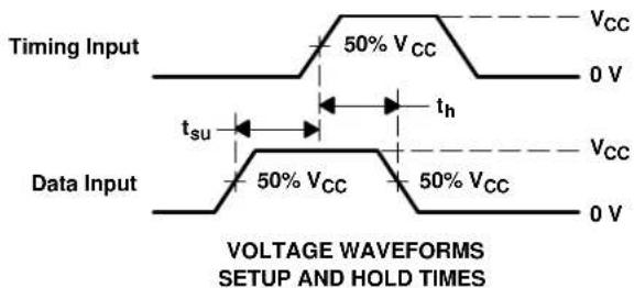
text_image
Timing Input 50% VCC VCC 0 V tsu th Data Input 50% VCC 50% VCC VCC 0 V VOLTAGE WAVEFORMS SETUP AND HOLD TIMES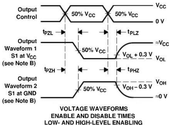
other
| Waveform | Time Label | Description | |----------|------------|----------------------------------| | Waveform 1 | S1 at Vcc (see Note B) | tPZL, tPLZ, ≈VCC, VOL + 0.3 V, VOL, tPHZ, VOH - 0.3 V | | Waveform 2 | S1 at GND (see Note B) | tPZH, tPHZ, ≈VCC, VOL + 0.3 V, VOH - 0.3 V |NOTES: A. C L includes probe and jig capacitance.
B. Waveform 1 is for an output with internal conditions such that the output is low, except when disabled by the output control. Waveform 2 is for an output with internal conditions such that the output is high, except when disabled by the output control.
C. All input pulses are supplied by generators having the following characteristics: PRR ≤ 1 MHz, Z O = 50 Ω, t r ≤ 3 ns, t f ≤ 3 ns.
D. The outputs are measured one at a time, with one input transition per measurement.
E. tPLZ and t_PHZ are the same as t_dis .
F. t_PZL and t_PZH are the same as t_en .
G. t_PHL and t_PLH are the same as t_pd .
H. All parameters and waveforms are not applicable to all devices.
Figure
- Load
Circuits
and
Voltage
PACKAGING INFORMATION
| Orderable Device Status(1) | Package Type | Package Drawing | Pins | Package Qty | Eco Plan(2) | Lead finish/ Ball material(6) | MSL Peak Temp(3) | Op Temp (°C) | Device Marking(4-5) | Samples | |
| SN74LV138AD ACTIVE SOIC D 16 40 RoHS & Green NIPDAU Level-1-260C- UNLIM -40 to 85 LV138A | Samples | ||||||||||
| SN74LV138ADBR | ACTIVE | SSOP | DB | 16 | 2000 | RoHS & Green | NIPDAU | Level-1-260C-UNLIM | -40 to 85 | LV138A | Samples |
| SN74LV138ADGVR | ACTIVE | TVSOP | DGV | 16 | 2000 | RoHS & Green | NIPDAU | Level-1-260C-UNLIM | -40 to 85 | LV138A | Samples |
| SN74LV138ADR | ACTIVE | SOIC | D | 16 | 2500 | RoHS & Green | NIPDAU | Level-1-260C-UNLIM | -40 to 85 | LV138A | Samples |
| SN74LV138ANSR | ACTIVE | SO | NS | 16 | 2000 | RoHS & Green | NIPDAU | Level-1-260C-UNLIM | -40 to 85 | 74LV138A | Samples |
| SN74LV138APW | ACTIVE | TSSOP | PW | 16 | 90 | RoHS & Green | NIPDAU | Level-1-260C-UNLIM | -40 to 85 | LV138A | Samples |
| SN74LV138APWG4 | ACTIVE | TSSOP | PW | 16 | 90 | RoHS & Green | NIPDAU | Level-1-260C-UNLIM | -40 to 85 | LV138A | Samples |
| SN74LV138APWR | ACTIVE | TSSOP | PW | 16 | 2000 | RoHS & Green | NIPDAU | SN | Level-1-260C-UNLIM | -40 to 85 | LV138A | Samples |
| SN74LV138APWRG4 | ACTIVE | TSSOP | PW | 16 | 2000 | RoHS & Green | NIPDAU | Level-1-260C-UNLIM | -40 to 85 | LV138A | Samples |
| SN74LV138APWT | ACTIVE | TSSOP | PW | 16 | 250 | RoHS & Green | NIPDAU | Level-1-260C-UNLIM | -40 to 85 | LV138A | Samples |
| SN74LV138ARGYR | ACTIVE | VQFN | RGY | 16 | 3000 | RoHS & Green | NIPDAU | Level-2-260C-1 YEAR | -40 to 85 | LV138A | Samples |
(1) The marketing status values are defined as follows:
ACTIVE: Product device recommended for new designs.
LIFEBUY: TI has announced that the device will be discontinued, and a lifetime-buy period is in effect.
NRND: Not recommended for new designs. Device is in production to support existing customers, but TI does not recommend using this part in a new design.
PREVIEW: Device has been announced but is not in production. Samples may or may not be available.
OBSOLETE: TI has discontinued the production of the device.
(2) RoHS: TI defines "RoHS" to mean semiconductor products that are compliant with the current EU RoHS requirements for all 10 RoHS substances, including the requirement that RoHS substance do not exceed 0.1% by weight in homogeneous materials. Where designed to be soldered at high temperatures, "RoHS" products are suitable for use in specified lead-free processes. TI may reference these types of products as "Pb-Free".
RoHS Exempt: TI defines "RoHS Exempt" to mean products that contain lead but are compliant with EU RoHS pursuant to a specific EU RoHS exemption.
Green: TI defines "Green" to mean the content of Chlorine (Cl) and Bromine (Br) based flame retardants meet JS709B low halogen requirements of <=1000ppm threshold. Antimony trioxide based flame retardants must also meet the <=1000ppm threshold requirement.
(3) MSL, Peak Temp. - The Moisture Sensitivity Level rating according to the JEDEC industry standard classifications, and peak solder temperature.
(4) There may be additional marking, which relates to the logo, the lot trace code information, or the environmental category on the device.
(5) Multiple Device Markings will be inside parentheses. Only one Device Marking contained in parentheses and separated by a "\~" will appear on a device. If a line is indented then it is a continuation of the previous line and the two combined represent the entire Device Marking for that device.
(6) Lead finish/Ball material - Orderable Devices may have multiple material finish options. Finish options are separated by a vertical ruled line. Lead finish/Ball material values may wrap to two lines if the finish value exceeds the maximum column width.
Important Information and Disclaimer: The information provided on this page represents TI's knowledge and belief as of the date that it is provided. TI bases its knowledge and belief on information provided by third parties, and makes no representation or warranty as to the accuracy of such information. Efforts are underway to better integrate information from third parties. TI has taken and continues to take reasonable steps to provide representative and accurate information but may not have conducted destructive testing or chemical analysis on incoming materials and chemicals. TI and TI suppliers consider certain information to be proprietary, and thus CAS numbers and other limited information may not be available for release.
In no event shall TI's liability arising out of such information exceed the total purchase price of the TI part(s) at issue in this document sold by TI to Customer on an annual basis.
TAPE AND REEL INFORMATION
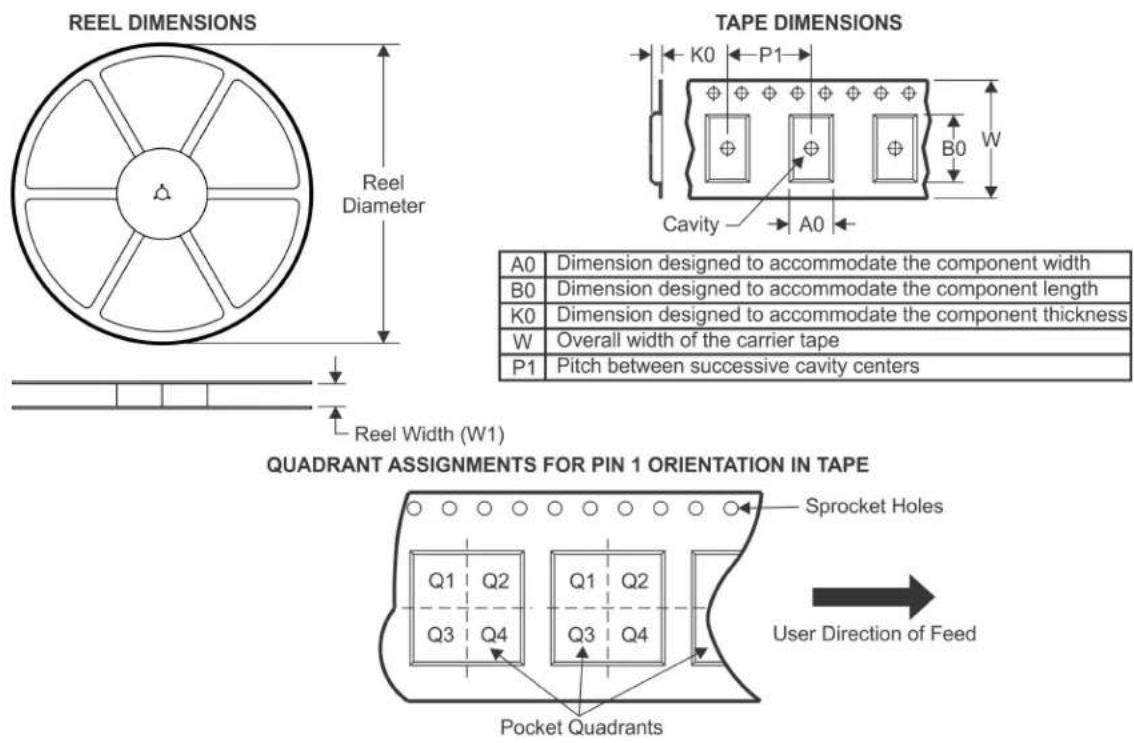
*All dimensions are nominal
| Device Package | Type | Package Drawing | Pins | SPQ Reel | Diameter (mm) | Reel Width W1 (mm) | A0 (mm) | B0 (mm) | K0 (mm) | P1 (mm) | W (mm) | Pin1 Quadrant |
| SN74LV138ADBR SSOP DB 16 | 2000 330.0 | 16.4 | 3.35 6.6 2.4 | 12.0 16.0 Q1 | ||||||||
| SN74LV138ADGVR TVSOP DGV | 16 2000 3 | 30.0 1 | 2.4 6.8 4.0 | 1.6 8.0 12.0 Q1 | ||||||||
| SN74LV138ADR SOIC D 16 250 | 0 330.0 | 16.4 6.5 | 10.3 2.1 8.0 | 16.0 Q1 | ||||||||
| SN74LV138ANSR SO | NS 16 2000 | 330.0 16.4 8.2 | 10.5 2.5 12.0 | 16.0 Q1 | ||||||||
| SN74LV138APWR | TSSOP PW | 16 2000 | 330.0 12.4 | 6.9 5.6 16 8.0 | 12.0 Q1 | |||||||
| SN74LV138APWR | TSSOP PW | 16 2000 | 330.0 12.4 | 6.9 5.6 16 8.0 | 12.0 Q1 | |||||||
| SN74LV138APWRG4 | TSSOP | PW | 16 | 2000 | 330.0 | 12.4 | 6.9 | 5.6 | 1.6 | 8.0 | 12.0 | Q1 |
| SN74LV138APWT | TSSOP | PW | 16 | 250 | 330.0 | 12.4 | 6.9 | 5.6 | 1.6 | 8.0 | 12.0 | Q1 |
| SN74LV138ARGYR | VQFN RGY | 16 300 0 330 | 0 12.4 3.8 | 4.3 1.5 8.0 | 12.0 Q1 |

text_image
TAPE AND REEL BOX DIMENSIONS W L*All dimensions are nominal
| Device | Package Type | Package Drawing | Pins | SPQ | Length (mm) | Width (mm) | Height (mm) |
| SN74LV138ADBR SSOP DB 16 2000 853.0 | 449.0 35.0 | ||||||
| SN74LV138ADGVR TVSOP DGV 16 2000 853.0 | 449.0 35.0 | ||||||
| SN74LV138ADR SOIC D 16 2500 | 340.5 336.1 32.0 | ||||||
| SN74LV138ANSR | SO | NS 16 2000 | 853.0 | 449.0 35.0 | |||
| SN74LV138APWR | TSSOP | PW | 16 | 2000 | 364.0 | 364.0 | 27.0 |
| SN74LV138APWR | TSSOP | PW | 16 | 2000 | 853.0 | 449.0 | 35.0 |
| SN74LV138APWRG4 | TSSOP | PW | 16 | 2000 | 853.0 | 449.0 | 35.0 |
| SN74LV138APWT | TSSOP | PW | 16 | 250 | 853.0 | 449.0 | 35.0 |
| SN74LV138ARGYR | VQFN | RGY 16 3000 | 853.0 | 449.0 35.0 |
TUBE
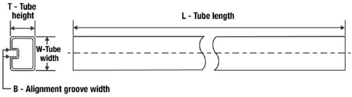
text_image
T - Tube height L - Tube length W - Tube width B - Alignment groove width*All dimensions are nominal
| Device | Package Name | Package Type | Pins | SPQ | L (mm) | W (mm) | T (μm) | B (mm) |
| SN74LV138AD D SO | C 16 40 507 8 3940 | 4.32 | ||||||
| SN74LV138APW PW | TSSOP 16 90 530 1 | 0.2 3600 3.5 | ||||||
| SN74LV138APWG4 PW | TSSOP 16 90 530 | 10.2 3600 3.5 |
SOP

4220735/A 12/2021
NOTES:
- All linear dimensions are in millimeters. Dimensions in parenthesis are for reference only. Dimensioning and tolerancing per ASME Y14.5M.
- This drawing is subject to change without notice.
- This dimension does not include mold flash, protrusions, or gate burrs. Mold flash, protrusions, or gate burrs shall not exceed 0.15 mm, per side.
- This dimension does not include interlead flash. Interlead flash shall not exceed 0.25 mm, per side.
SOP

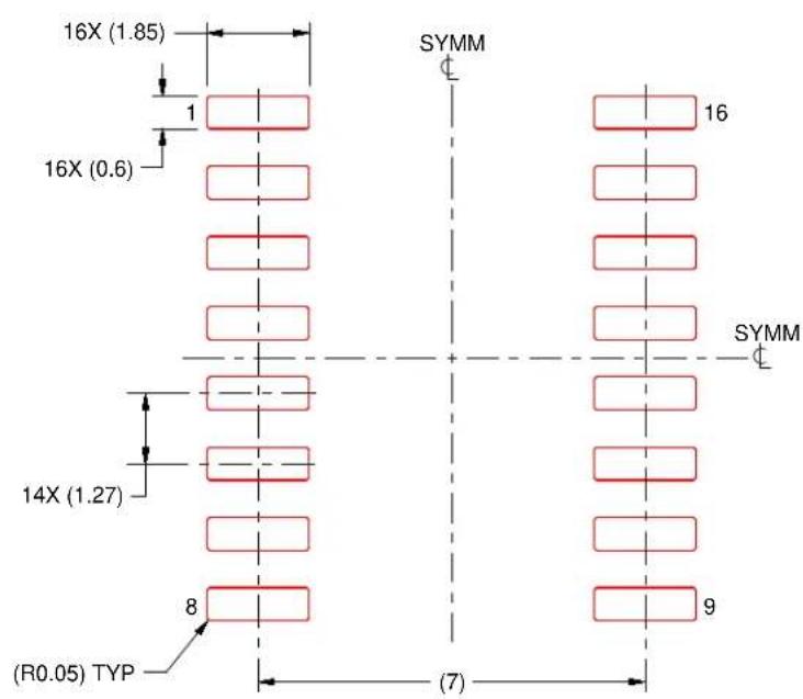
text_image
16X (1.85) 1 16X (0.6) SYMM SEE DETAILS 16 SYMM 14X (1.27) 8 (R0.05) TYP 9 (7)LAND PATTERN EXAMPLE SCALE:7X
text_image
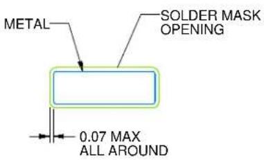
METAL SOLDER MASK OPENING 0.07 MAX ALL AROUNDNON SOLDER MASK DEFINED

text_image
SOLDER MASK OPENING METAL 0.07 MIN ALL AROUNDSOLDER MASK
DEFINED
SOLDER MASK DETAILS
4220735/A 12/2021
NOTES: (continued)
- Publication IPC-7351 may have alternate designs.
- Solder mask tolerances between and around signal pads can vary based on board fabrication site.
SOP
text_image
16X (1.85) 1 16X (0.6) 14X (1.27) 8 (R0.05) TYP SYMM 16 SYMM 9 (7)SOLDER PASTE EXAMPLE BASED ON 0.125 mm THICK STENCIL SCALE:7X
4220735/A 12/2021
NOTES: (continued)
- Laser cutting apertures with trapezoidal walls and rounded corners may offer better paste release. IPC-7525 may have alternate design recommendations.
- Board assembly site may have different recommendations for stencil design.
D (R-PDSO-G16)
PLASTIC SMALL OUTLINE
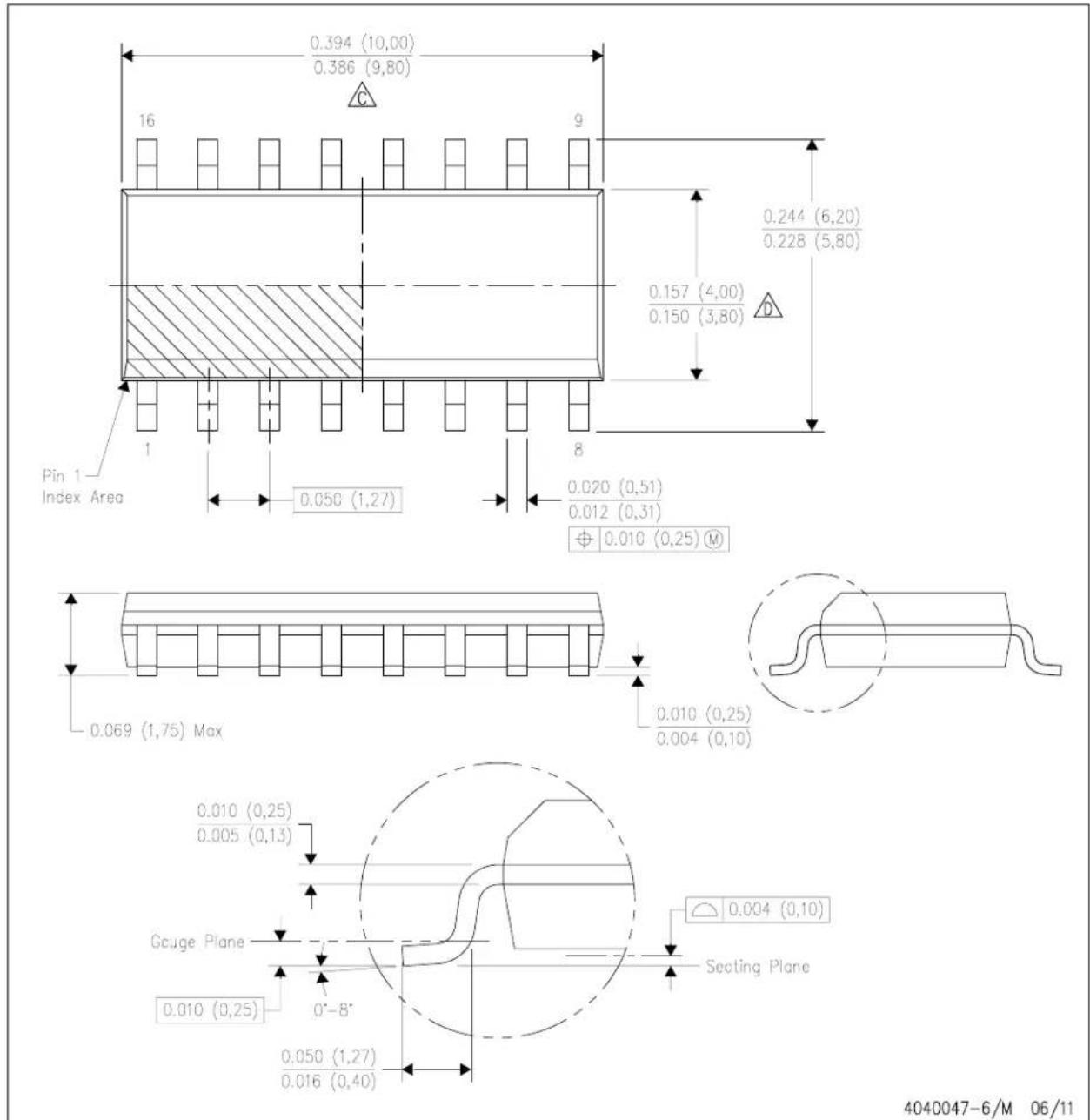
text_image
0.394 (10,00) 0.386 (9,80) 16 9 0.244 (6,20) 0.228 (5,80) 0.157 (4,00) 0.150 (3,80) Pin 1 Index Area 1 8 0.050 (1,27) 0.020 (0,51) 0.012 (0,31) ⊕ 0.010 (0,25) M 0.069 (1,75) Max 0.010 (0,25) 0.004 (0,10) Gcuge Plane 0.010 (0,25) 0.005 (0,13) 0'-8" Seating Plane 0.010 (0,25) 0.050 (1,27) 0.016 (0,40) 4040047-6/M 06/11NOTES: A. All linear dimensions are in inches (millimeters).
B. This drawing is subject to change without notice.
Body length does not include mold flash, protrusions, or gate burrs. Mold flash, protrusions, or gate burrs shall not exceed 0.006 (0,15) each side.
Body width does not include interlead flash. Interlead flash shall not exceed 0.017 (0,43) each side.
E. Reference JEDEC MS-012 variation AC.
D (R-PDSO-G16)
4211283-4/E 08/12
NOTES: A. All linear dimensions are in millimeters.
B. This drawing is subject to change without notice.
C. Publication IPC-7351 is recommended for alternate designs.
D. Laser cutting apertures with trapezoidal walls and also rounding corners will offer better paste release. Customers should contact their board assembly site for stencil design recommendations. Refer to IPC-7525 for other stencil recommendations.
E. Customers should contact their board fabrication site for solder mask tolerances between and around signal pads.
SMALL OUTLINE PACKAGE
4220204/A 02/2017
NOTES:
- All linear dimensions are in millimeters. Any dimensions in parenthesis are for reference only. Dimensioning and tolerancing per ASME Y14.5M.
- This drawing is subject to change without notice.
- This dimension does not include mold flash, protrusions, or gate burrs. Mold flash, protrusions, or gate burrs shall not exceed 0.15 mm per side.
- This dimension does not include interlead flash. Interlead flash shall not exceed 0.25 mm per side.
- Reference JEDEC registration MO-153.
SMALL OUTLINE PACKAGE
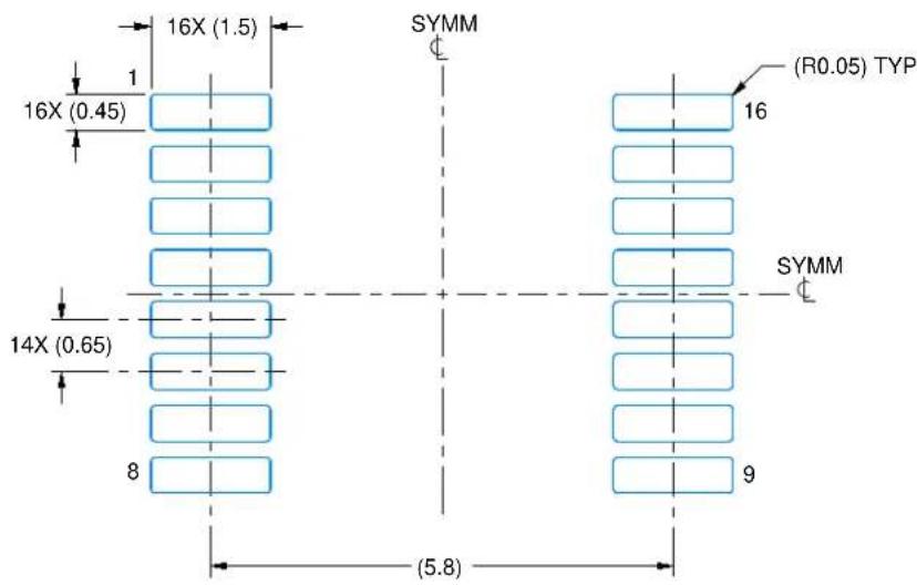
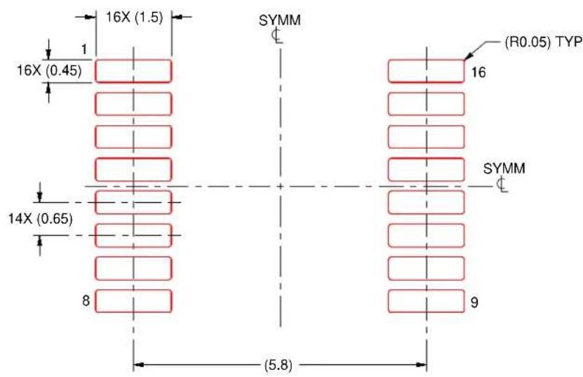
text_image
16X (1.5) 1 16X (0.45) 14X (0.65) 8 (5.8) SYMM (R0.05) TYP 16 SYMM 9LAND PATTERN EXAMPLE
EXPOSED METAL SHOWN
SCALE: 10X
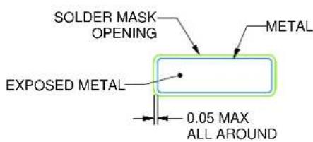
text_image
SOLDER MASK OPENING METAL EXPOSED METAL 0.05 MAX ALL AROUNDNON-SOLDER MASK DEFINED (PREFERRED)
text_image
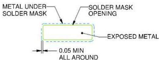
METAL UNDER SOLDER MASK SOLDER MASK OPENING EXPOSED METAL 0.05 MIN ALL AROUNDSOLDER MASK
DEFINED
SOLDER MASK DETAILS
4220204/A 02/2017
NOTES: (continued)
- Publication IPC-7351 may have alternate designs.
- Solder mask tolerances between and around signal pads can vary based on board fabrication site.
SMALL OUTLINE PACKAGE
text_image
16X (1.5) 1 16X (0.45) SYMM (R0.05) TYP 16 SYMM 14X (0.65) 8 (5.8)SOLDER PASTE EXAMPLE
BASED ON 0.125 mm THICK STENCIL
SCALE: 10X
4220204/A 02/2017
NOTES: (continued)
- Laser cutting apertures with trapezoidal walls and rounded corners may offer better paste release. IPC-7525 may have alternate design recommendations.
- Board assembly site may have different recommendations for stencil design.
SMALL OUTLINE PACKAGE

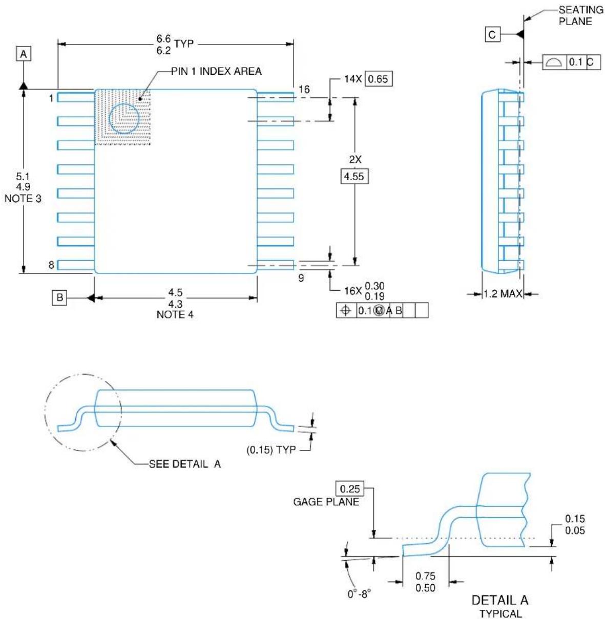
text_image
A 8.2 TYP 7.4 PIN 1 INDEX AREA 16 14X 0.65 6.5 5.9 NOTE 3 2X 4.55 8 9 16X 0.38 0.22 B 5.6 5.0 NOTE 4 ⊕ 0.1@ A B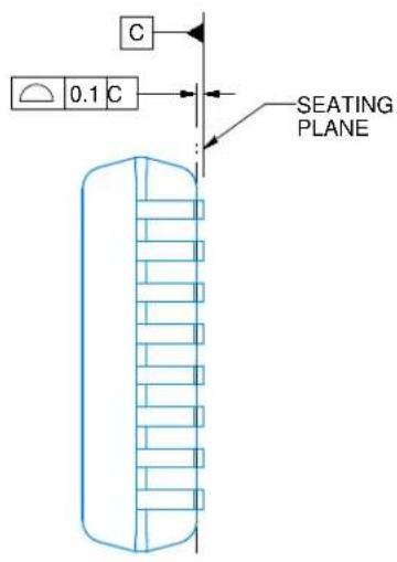
text_image
C 0.1 C SEATING PLANE
text_image
0.25 0.09 SEE DETAIL A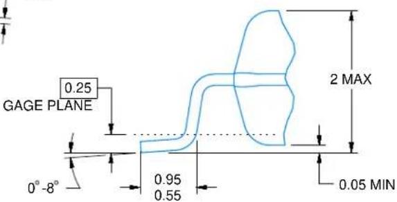
text_image
GAGE PLANE 0.25 0°-8° 0.95 0.55 2 MAX 0.05 MINDETAIL A TYPICAL
4220763/A 05/2022
NOTES:
- All linear dimensions are in millimeters. Any dimensions in parenthesis are for reference only. Dimensioning and tolerancing per ASME Y14.5M.
- This drawing is subject to change without notice.
- This dimension does not include mold flash, protrusions, or gate burrs. Mold flash, protrusions, or gate burrs shall not exceed 0.15 mm per side.
- Reference JEDEC registration MO-150.
SMALL OUTLINE PACKAGE
text_image
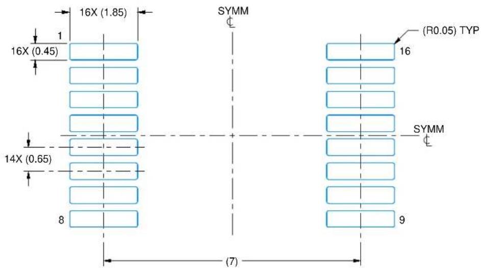
16X (1.85) SYMM (0.05) TYP 16 16X (0.45) 14X (0.65) 8 (7) 9 SYMMLAND PATTERN EXAMPLE
EXPOSED METAL SHOWN
SCALE: 10X
text_image
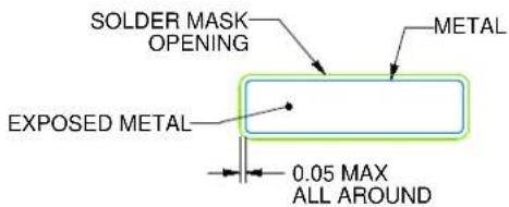
SOLDER MASK OPENING METAL EXPOSED METAL 0.05 MAX ALL AROUNDNON-SOLDER MASK
DEFINED
(PREFERRED)

text_image
METAL UNDER SOLDER MASK SOLDER MASK OPENING EXPOSED METAL 0.05 MIN ALL AROUNDSOLDER MASK
DEFINED
SOLDER MASK DETAILS
4220763/A 05/2022
NOTES: (continued)
- Publication IPC-7351 may have alternate designs.
- Solder mask tolerances between and around signal pads can vary based on board fabrication site.
SMALL OUTLINE PACKAGE
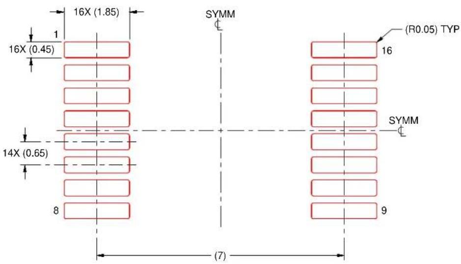
text_image
16X (1.85) 1 16X (0.45) SYMM (R0.05) TYP 16 14X (0.65) 8 SYMM 9 (7)SOLDER PASTE EXAMPLE
BASED ON 0.125 mm THICK STENCIL
SCALE: 10X
4220763/A 05/2022
NOTES: (continued)
- Laser cutting apertures with trapezoidal walls and rounded corners may offer better paste release. IPC-7525 may have alternate design recommendations.
- Board assembly site may have different recommendations for stencil design.
MECHANICAL DATA
NS (R-PDSO-G\*\*)
PLASTIC SMALL-OUTLINE PACKAGE
14-PINS SHOWN

text_image
1,27 14 0,51 0,35 Ø 0,25① 8 5,60 5,00 8,20 7,40 1 7 A
text_image
0,15 NOM Gage Plane 0,25 0°-10° 1,05 0,55
text_image
2,00 MAX 0,15 0,05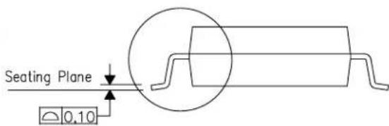
text_image
Seating Plane 0.10| DIM\PINS ** | 14 | 16 | 20 | 24 |
| A MAX | 10,50 | 10,50 | 12,90 | 15,30 |
| A MIN | 9,90 | 9,90 | 12,30 | 14,70 |
4040062/C 03/03
NOTES: A. All linear dimensions are in millimeters.
B. This drawing is subject to change without notice.
C. Body dimensions do not include mold flash or protrusion, not to exceed 0,15.
DGV (R-PDSO-G\*\*) PLASTIC SMALL-OUTLINE
24 PINS SHOWN

| DIM\PINS ** | 14 | 20 | 382416 | 48 | 56 | ||
| A MAX | 3,70 | 5,10 | 5,103,70 | 7,90 | 9,80 | 11,40 | |
| A MIN | 3,50 | 3,50 | 4,90 | 4,90 | 7,70 | 9,60 | 11,20 |
4073251/E 08/00
NOTES: A. All linear dimensions are in millimeters.
B. This drawing is subject to change without notice.
C. Body dimensions do not include mold flash or protrusion, not to exceed 0.15 per side.
D. Falls within JEDEC: 24/48 Pins - MO-153
14/16/20/56 Pins - MO-194
RGY (R-PVQFN-N16)
PLASTIC QUAD FLATPACK NO-LEAD
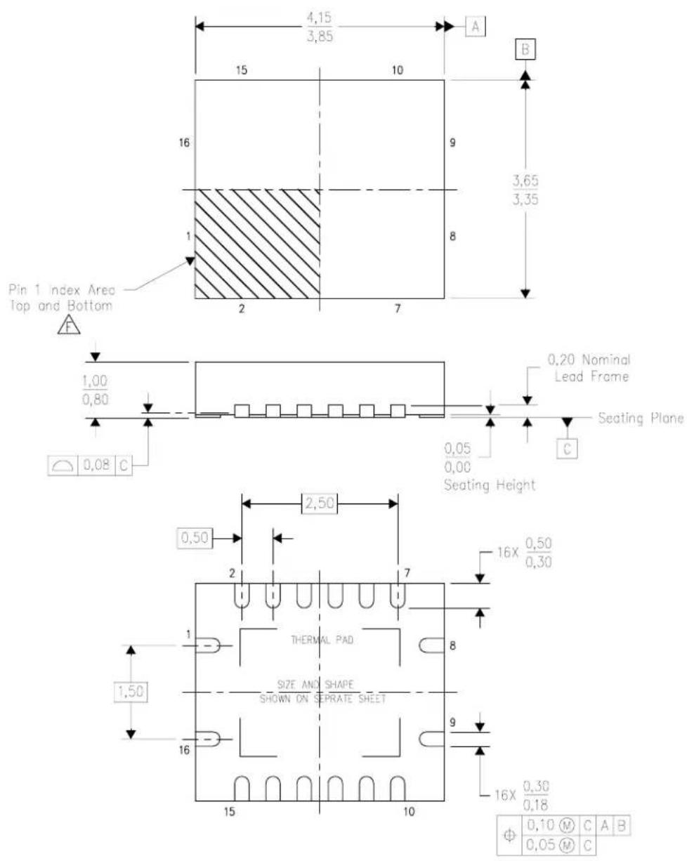
text_image
4,15 3,85 A 15 10 16 9 3,65 3,35 1 2 7 Pin 1 Index Area Top and Bottom F 1,00 0,80 0,08 C 0,20 Nominal Lead Frame Seating Plane C 0,05 0,00 Seating Height 2,50 0,50 2 7 16X 0,50 0,30 1 1,50 16 SIZE AND SHAPE SHOWN ON SEPRATE SHEET 9 16X 0,30 0,18 Φ 0,10 M C A B 0,05 M CBottom View
4203539-3/1 06/2011
NOTES: A. All linear dimensions are in millimeters. Dimensioning and tolerancing per ASME Y14.5M-1994.
B. This drawing is subject to change without notice.
C. QFN (Quad Flatpack No-Lead) package configuration.
D. The package thermal pad must be soldered to the board for thermal and mechanical performance.
E. See the additional figure in the Product Data Sheet for details regarding the exposed thermal pad features and dimensions.
Pin 1 identifiers are located on both top and bottom of the package and within the zone indicated.
The Pin 1 identifiers are either a molded, marked, or metal feature.
G. Package complies to JEDEC MO-241 variation BA.
RGY (R-PVQFN-N16)
PLASTIC QUAD FLATPACK NO-LEAD
THERMAL INFORMATION
This package incorporates an exposed thermal pad that is designed to be attached directly to an external heatsink. The thermal pad must be soldered directly to the printed circuit board (PCB). After soldering, the PCB can be used as a heatsink. In addition, through the use of thermal vias, the thermal pad can be attached directly to the appropriate copper plane shown in the electrical schematic for the device, or alternatively, can be attached to a special heatsink structure designed into the PCB. This design optimizes the heat transfer from the integrated circuit (IC).
For information on the Quad Flatpack No-Lead (QFN) package and its advantages, refer to Application Report, QFN/SON PCB Attachment, Texas Instruments Literature No. SLUA271. This document is available at www.ti.com.
The exposed thermal pad dimensions for this package are shown in the following illustration.
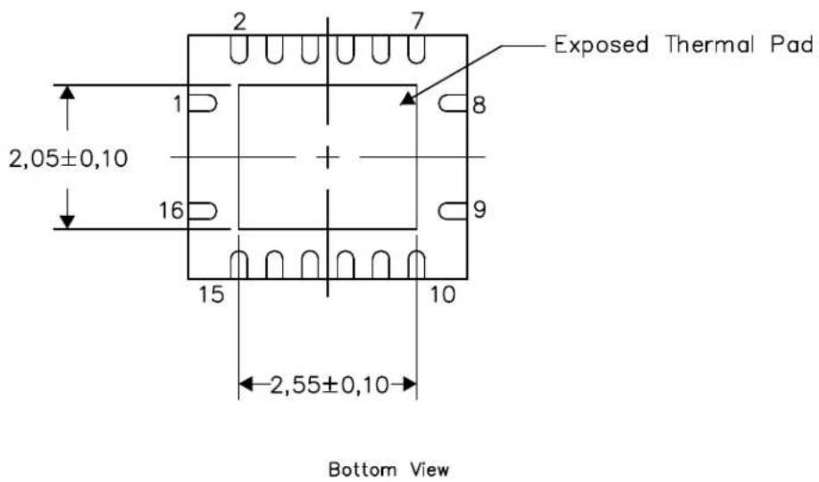
text_image
2 7 Exposed Thermal Pad 1 8 2,05±0,10 16 9 15 10 2,55±0,10 Bottom ViewExposed Thermal Pad Dimensions
4206353-3/P 03/14
NOTE: All linear dimensions are in millimeters
RGY (R-PVQFN-N16)
PLASTIC QUAD FLATPACK NO-LEAD
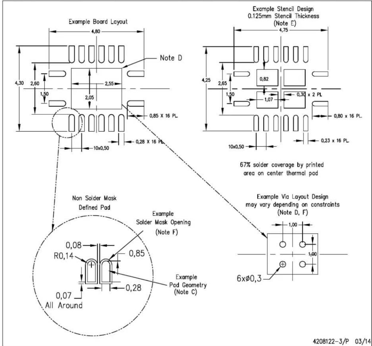
text_image
Example Board Layout 4,80 Note D 4,30 2,60 1,50 2,05 0,85 x 16 PL 10x0,50 0,28 x 16 PL Non Solder Mask Defined Pad R0,14 0,07 All Around Example Solder Mask Opening (Note F) 0,85 0,28 Example Pad Geometry (Note C) Example Stencil Design 0.125mm Stencil Thickness (Note E) 4,75 4,25 2,65 1,50 1,07 0,30 x 2 PL 0,82 1,07 0,80 x 16 PL 10x0,50 0,23 x 16 PL 67% solder coverage by printed area on center thermal pad Example Via Layout Design may vary depending on constraints (Note D, F) 6xØ0,3 4208122-3/P 03/14NOTES: A. All linear dimensions are in millimeters.
B. This drawing is subject to change without notice.
C. Publication IPC-7351 is recommended for alternate designs.
D. This package is designed to be soldered to a thermal pad on the board. Refer to Application Note, Quad Flat-Pack QFN/SON PCB Attachment, Texas Instruments Literature No. SLUA271, and also the Product Data Sheets for specific thermal information, via requirements, and recommended board layout. These documents are available at www.ti.com http://www.ti.com.
E. Laser cutting apertures with trapezoidal walls and also rounding corners will offer better paste release. Customers should contact their board assembly site for stencil design recommendations. Refer to IPC 7525 for stencil design considerations.
F. Customers should contact their board fabrication site for minimum solder mask web tolerances between signal pads.
IMPORTANT NOTICE AND DISCLAIMER
TI PROVIDES TECHNICAL AND RELIABILITY DATA (INCLUDING DATA SHEETS), DESIGN RESOURCES (INCLUDING REFERENCE DESIGNS), APPLICATION OR OTHER DESIGN ADVICE, WEB TOOLS, SAFETY INFORMATION, AND OTHER RESOURCES "AS IS" AND WITH ALL FAULTS, AND DISCLAIMS ALL WARRANTIES, EXPRESS AND IMPLIED, INCLUDING WITHOUT LIMITATION ANY IMPLIED WARRANTIES OF MERCHANTABILITY, FITNESS FOR A PARTICULAR PURPOSE OR NON-INFRINGEMENT OF THIRD PARTY INTELLECTUAL PROPERTY RIGHTS.
These resources are intended for skilled developers designing with TI products. You are solely responsible for (1) selecting the appropriate TI products for your application, (2) designing, validating and testing your application, and (3) ensuring your application meets applicable standards, and any other safety, security, regulatory or other requirements.
These resources are subject to change without notice. TI grants you permission to use these resources only for development of an application that uses the TI products described in the resource. Other reproduction and display of these resources is prohibited. No license is granted to any other TI intellectual property right or to any third party intellectual property right. TI disclaims responsibility for, and you will fully indemnify TI and its representatives against, any claims, damages, costs, losses, and liabilities arising out of your use of these resources.
TI's products are provided subject to TI's Terms of Sale or other applicable terms available either on ti.com or provided in conjunction with such TI products. TI's provision of these resources does not expand or otherwise alter TI's applicable warranties or warranty disclaimers for TI products.
TI objects to and rejects any additional or different terms you may have proposed.
Mailing Address: Texas Instruments, Post Office Box 655303, Dallas, Texas 75265
Copyright © 2022, Texas Instruments Incorporated