SN74LVC3G17DCUR - Electronic component TEXAS INSTRUMENTS - Free user manual and instructions
Find the device manual for free SN74LVC3G17DCUR TEXAS INSTRUMENTS in PDF.

User questions about SN74LVC3G17DCUR TEXAS INSTRUMENTS
0 question about this device. Answer the ones you know or ask your own.
Ask a new question about this device
Download the instructions for your Electronic component in PDF format for free! Find your manual SN74LVC3G17DCUR - TEXAS INSTRUMENTS and take your electronic device back in hand. On this page are published all the documents necessary for the use of your device. SN74LVC3G17DCUR by TEXAS INSTRUMENTS.
USER MANUAL SN74LVC3G17DCUR TEXAS INSTRUMENTS
SN74LVC3G17TripleSchmitt-TriggerBuffer
1Features3Description
•AvailableintheTexasInstruments NanoFree™Package
•Supports5-VV cc Operation
- InputsAcceptVoltagesto5.5V
•Maximumt pd of5.4nsat3.3V
•LowPowerConsumption,10-μAMaximuml cc
- ±24-mAOutputDriveat3.3V
•TypicalV OLP (OutputGroundBounce)
<0.8VatV CC =3.3V,T A=25°C
•TypicalV OHV (OutputV OH Undershoot)
2VatV CC =3.3V,T A =25°C
- I_off SupportsLiveInsertion, Partial-Power-Down ModeandBackDriveProtection
- Latch-UpPerformanceExceeds100mA PerJESD78,ClassII
- ESDProtectionExceedsJESD22 - 2000-VHumanBodyModel(A114-A) - 200-VMachineModel(A115-A) - 1000-VCharged-DeviceModel(C101)
2Applications
•AVReceivers
•AudioDocks:Portable
- Blu-ray ® PlayersandHomeTheater
•MP3Players/Recorders
•PersonalDigitalAssistants(PDAs)
•Power:Telecom/ServerAC/DCSupply:Single Controller:AnalogandDigital
•SolidStateDrives(SSDs):ClientandEnterprise
•TVs:LCD/DigitalandHigh-Definition(HDTVs)
•Tablets:Enterprise
•VideoAnalytics:Server
•WirelessHeadsets,Keyboards,andMice
ThistripleSchmitt-triggerbufferisdesignedfor 1.65-Vto5.5-VV CC operation.
TheSN74LVC3G17devicecontainsthreebuffers and performstheBooleanfunctionY=A.Thedevice functionsasthreeindependentbuffersbut,because of Schmittaction,itmayhavedifferentinputthreshold levels for positive-going ( V_T+ ) and negative-going ( V_T- )signals.
This device is fully specified for partial-power-down applications using I_off . The I_off circuitry disables the outputs, preventing damaging current backflow through the device when it is powered down.
NanoFree package technology is a major breakthrough in C packaging concepts, using the die asthe package.
DeviceInformation (1)
| PART NUMBER | PACKAGE | BODY SIZE (NOM) |
| SN74LVC3G17DCT | SSOP (8) | 2.95 mm × 2.80 mm |
| SN74LVC3G17DCU | VSSOP (8) | 2.30 mm × 2.00 mm |
| SN74LVC3G17YZP | DSBGA (8) | 1.91 mm × 0.91 mm |
(1) For all available packages, see the orderable addendum at the end of the data sheet.
SimplifiedSchematic
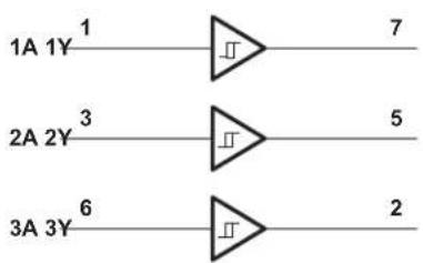
flowchart
graph LR
    A["1A 1Y"] --> B["1"]
    B --> C["7"]
    D["2A 2Y"] --> E["3"]
    E --> F["5"]
    G["3A 3Y"] --> H["6"]
    H --> I["2"]
TableofContents
1 Features.... 1
2 Applications 1
3 Description 1
4 Revision History...... 2
5PinConfigurationandFunctions....3
6 Specifications.... 4
6.1 AbsoluteMaximumRatings....4
6.2ESDRatings....4
6.3RecommendedOperatingConditions....4
6.4ThermalInformation....5
6.5 Electrical Characteristics....5
6.6SwitchingCharacteristics....6
6.7OperatingCharacteristics....6
6.8TypicalCharacteristics....6
7ParameterMeasurementInformation....7
8DetailedDescription....9
8.1 Overview....9
8.2FunctionalBlockDiagram....9
8.3FeatureDescription....9
8.4DeviceFunctionalModes....9
9ApplicationandImplementation....10
9.1 Application Information....10
9.2 Typical Application....10
10PowerSupplyRecommendations....11
11 Layout.... 11
11.1 LayoutGuidelines....11
11.2LayoutExample....12
12DeviceandDocumentationSupport....13
12.1 DocumentationSupport....13
12.2 Community Resources....13
12.3Trademarks....13
12.4ElectrostaticDischargeCaution....13
12.5Glossary....13
13Mechanical, Packaging, and Orderable Information 13
4RevisionHistory
NOTE: Pagenumbersforpreviousrevisionsmaydifferfrompagenumbersinthecurrentversion.
ChangesfromRevisionE(November2013)toRevisionF
Page
- Added the Device Information table, ESD Ratings table, Feature Description section, Device Functional Modes, Application and Implementation section, Power Supply Recommendations section, Layout section, Device and Documentation Support section, and Mechanical, Packaging, and Orderable Information section.... 1
- MovedT _stg to Absolute Maximum Ratings table.... 4
ChangesfromRevisionD(Feburary2007)toRevisionE
Page
- Updated document to new TI data sheet format.... 1
- Updated operating temperature range. 4
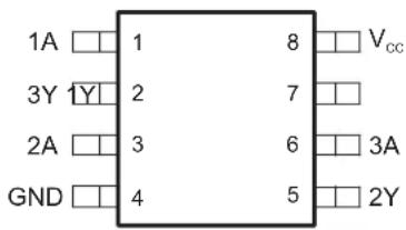
5PinConfigurationandFunctions
DCT Package
8-Pin SSOP
Top View
text_image
1A 1 8 Vcc 3Y 1Y 2 7 2A 3 6 3A GND 4 5 2YDCU Package
8-Pin VSSOP
Top View
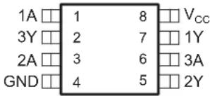
text_image
1A □ 1 8 □ Vcc 3Y □ 2 7 □ 1Y 2A □ 3 6 □ 3A GND □ 4 5 □ 2YYZP Package
8-Pin DSBGA
Bottom View
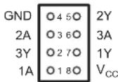
See mechanical drawing for dimensions.
PinFunctions
| PIN | TYPE | DESCRIPTION | |
| NAME | NO. | ||
| 1A | 1 | I | Input 1 |
| 1Y | 7 | O | Output 1 |
| 2A | 3 | I | Input 2 |
| 2Y | 5 | O | Output 2 |
| 3A | 6 | I | Input 3 |
| 3Y | 2 | O | Output 3 |
| GND | 4 | — | Ground |
| V_CC | 8 | — | Power Pin |
6Specifications
6.1 AbsoluteMaximumRatings
overoperatingfree-airtemperaturerange(unlessotherwisenoted) (1)
| MINMAXUNIT | ||||
| V_CC | Supplyvoltage-0.56.5V | |||
| V_I | Inputvoltage(2) | -0.56.5V | ||
| V_O | Voltageappliedtoanyoutputinthehigh-impedanceorpower-offstate(2) | -0.56.5V | ||
| V_O | Outputvoltage(2)(3) | -0.5V CC+0.5V | ||
| I_IK | InputclampcurrentV | <0-50mA | ||
| I_OK | Outputclampcurrent | V O <0 | -50mA | |
| I_O | Continuousoutputcurrent | ±50mA | ||
| ContinuouscurrentthroughV CC orGND | ±100 | mA | ||
| T_stg | Storagetemperature | -65150°C | ||
(1) Stresses beyond those listed under Absolute Maximum Ratings may cause permanent damage to the device. These are stress ratings only, and functional operation of the device at these or any other conditions beyond those indicated under Recommended Operating Conditions is not implied. Exposure to absolute-maximum-rated conditions for extended periods may affect device reliability.
(2) The input negative-voltage and output voltage ratings may be exceeded if the input and output current ratings are observed.
(3) ThevalueofV CC isprovidedintheRecommendedOperatingConditionstable.
6.2ESDRatings
| VALUE | UNIT | |||
| V_ESD | Electrostatic discharge | HumanBodyModel(HBM),perANSI/ESDA/JEDECJS-001,allpins(1) | +2000 | V |
| Charged-DeviceModel(CDM),perJEDECspecificationJESD22-C101,allpins(2) | +1000 | |||
(1) JEDEC document JEP155 states that 500-V HBM allows safe manufacturing with a standard ESD control process.
(2) JEDEC document JEP157 states that 250-V CDM allows safe manufacturing with a standard ESD control process.
6.3 Recommended Operating Conditions
See ^(1) .
| MIN | MAX | UNIT | |||
| V_CC | Supplyvoltage | Operating | 1.655.5 | V | |
| V_I | Inputvoltage | 05.5 | V | ||
| V_O | Outputvoltage | 0 | V_CC | V | |
| I_OH | High-leveloutputcurrent | V_CC=1.65V | -4 | mA | |
| V_CC=2.3V | -8 | ||||
| V_CC=3V | -16 | ||||
| -24 | |||||
| V_CC=4.5V | -32 | ||||
| I_OL | Low-leveloutputcurrent | V_CC=1.65V | 4 | mA | |
| V_CC=2.3V | 8 | ||||
| V_CC=3V | 16 | ||||
| 24 | |||||
| V_CC=4.5V | 32 | ||||
| T_A | Operating free-air temperature | -40 | 125 | °C | |
(1) AllunusedinputsofthedevicemustbeheldatV CC orGNDtoensureproperdeviceoperation.RefertotheTlapplicationreport, ImplicationsofSloworFloatingCMOSInputs,SCBA004.
6.4ThermalInformation
| THERMALMETRIC (1) | SNLVC3G17 | ||||
| DCT(SSOP)DC | CU(VSSOP)YZP( | DSBGA)UNIT | |||
| 6PINS6PIN | 6PINS | ||||
| R_{\theta JA}$ | Junction-to-ambientthermalresistance (2) | 220227102°C/W | |||
(1) For more information about traditional and new thermal metrics, see the Semiconductor and IC Package Thermal Metrics application report, SPRA953.
(2) The packagethermalimpedance is calculated in accordance with JESD51-7.
6.5 Electrical Characteristics
overrecommendedoperatingfree-airtemperaturerange(unlessotherwisenoted)
| PARAMETERTEST CONDITIONS V | cc | -40°C to 85°C - 40°C to 125°C | UNIT | |||||
| MIN | TYP(1) | MAX | MIN | TYP(1) | MAX | |||
| V_T+ Positive-going inputthreshold voltage | 1.65 V | 0.79 | 1.16 | 0.79 | 1.16 | V | ||
| 2.3 V | 1.11 | 1.56 | 1.11 | 1.56 | ||||
| 3 V | 1.5 | 1.87 | 1.5 | 1.87 | ||||
| 4.5 V | 2.16 | 2.74 | 2.16 | 2.74 | ||||
| 5.5 V | 2.61 | 3.33 | 2.61 | 3.33 | ||||
| V_T- Negative-going inputthreshold voltage | 1.65 V | 0.39 | 0.62 | 0.39 | 0.62 | V | ||
| 2.3 V | 0.58 | 0.87 | 0.58 | 0.87 | ||||
| 3 V | 0.84 | 1.14 | 0.84 | 1.14 | ||||
| 4.5 V | 1.41 | 1.79 | 1.41 | 1.79 | ||||
| 5.5 V | 1.87 | 2.29 | 1.87 | 2.29 | ||||
| V_T Hysteresis V_T+-V_T- | 1.65 V | 0.37 | 0.62 | 0.37 | 0.62 | V | ||
| 2.3 V | 0.48 | 0.77 | 0.48 | 0.77 | ||||
| 3 V | 0.56 | 0.87 | 0.56 | 0.87 | ||||
| 4.5 V | 0.71 | 1.04 | 0.71 | 1.04 | ||||
| 5.5 V | 0.71 | 1.11 | 0.71 | 1.11 | ||||
| V_OH | I_OH=-100μA | 1.65V to 5.5VV | cc-0.1 | V_CC-0.1 | V | |||
| I_OH=-4mA | 1.65V | 1.2 | 1.2 | |||||
| I_OH=-8mA | 2.3V | 1.9 | 1.9 | |||||
| I_OH=-16mA | 3 V | 2.4 | 2.4 | |||||
| I_OH=-24mA | 2.3 | 2.3 | ||||||
| I_OH=-32mA | 4.5V | 3.8 | 3.8 | |||||
| V_OL | I_OL=100μA | 1.65 V to 5.5 V | 0.1 | 0.1 | V | |||
| I_OL=4mA | 1.65V | 0.45 | 0.45 | |||||
| I_OL=8mA | 2.3V | 0.3 | 0.3 | |||||
| I_OL=16mA | 3 V | 0.4 | 0.4 | |||||
| I_OL=24mA | 0.55 | 0.75 | ||||||
| I_OL=32mA | 4.5V | 0.55 | 0.75 | |||||
| I_I | V_I=5.5 V or GND | 0 to 5.5 V | ±1 | ±5 | μA | |||
| I_off | V_I or V_O=5.5 V | 0 | ±5 | ±10 | μA | |||
| I_CC | V_I=5.5VorGND,I_o=0 | 1.65 V to 5.5 V | 10 | 10 | μA | |||
| I_CC | Oneinputat V_CC-0.6V, OtherinputsatV_CC orGND | 3 V to 5.5 V | 500 | 500 | μA | |||
| C_I | V_I=V_CC orGND | 3.3V | 4 | pF | ||||
(1) AlltypicalvaluesareatV
CC=3.3V,T A=25°C.
6.6 Switching Characteristics
overrecommendedoperatingfree-airtemperaturerange,C =30pFor50pF(unlessotherwisenoted)
| PARAMETERTEST CONDITIONS | FROMTOV(INPUT) | CONDITIONSUNIT(OUTPUT) | -40°Cto85°C | |||||||||
| _cc =1.8VV± 0.15 V | _cc =2.5VV± 0.2 V | _cc =3.3VV± 0.3 V | _cc =5V± 0.5 V | |||||||||
| MIN | MAX | MIN | MAX | MIN | MAX | MIN | MAX | |||||
| t_pd | A | Y | See Figure 3 | 4.3 | 9.2 | 2 | 6.2 | 1.2 | 5.4 | 1 | 4.1 | ns |
| See Figure 3 | 4.3 | 10.2 | 2 | 7.2 | 1.2 | 6.4 | 1 | 5.1 | ||||
6.7 Operating Characteristics
T_A = 25^
| PARAMETER | TEST CONDITIONS | V_CC = 1.8 V | V_CC = 2.5 V | V_CC = 3.3 VV | _cc = 5 V | UNIT | |
| TYP | TYP | TYP | TYP | ||||
| C_pd | Power dissipation capacitance | f = 10 MHz | 18 | 19 | 19 | 22 | pF |
6.8TypicalCharacteristics

line
| Voltage (V) | Max tpd (ns) | |-------------|--------------| | 4.00 | 10.00 | | 5.00 | 7.00 | | 6.00 | 5.00 |Figure 1. Maximum Propagation vs Delay V_cc Voltage
7 ParameterMeasurementInformation
text_image
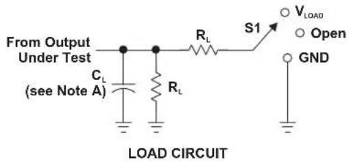
From Output Under Test (see Note A) C_L R_L S1 V_LOAD Open GND LOAD CIRCUIT| TEST S1 | |
| t_PLH/t_PHL | Open |
| t_PLZ/t_PZL | V_LOAD |
| t_PHZ/t_PZH | GND |
| V_cc | INPUTS | V_M | V_LOAD | C_L | R_L | V_A | |
| V_I | t_r/t_f | ||||||
| 1.8 V 0.15 V_± | V_cc | ≤2 ns | V_cc/2 | 2 × V_cc | 15 pF | 1 MΩ | 0.15 V |
| 2.5 V 0.2 V_± | V_cc | ≤2 ns | V_cc/2 | 2 × V_cc | 15 pF | 1 MΩ | 0.15 V |
| 3.3 V 0.3 V_± | 3 V | ≤2.5 ns | 1.5 V | 6 V | 15 pF | 1 MΩ | 0.3 V |
| 5 V 0.5 V_± | V_cc | ≤2.5 ns | V_cc/2 | 2 × V_cc | 15 pF | 1 MΩ | 0.3 V |
text_image
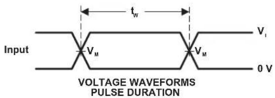
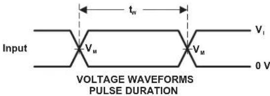
Input VOLTEG WAVEFORMS PULSE DURATION t_w V_M V_M 0 V V_i
text_image
Timing Input V_M 0 V t_{su} t_n Data Input V_M V_M 0 V VOLTAGE WAVEFORMS SETUP AND HOLD TIMES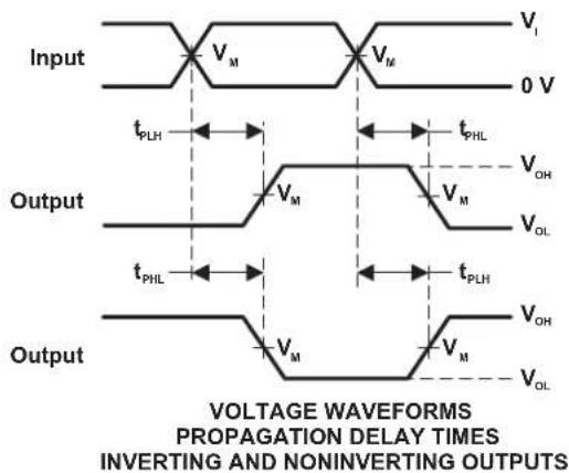
text_image
Input V_M 0 V t_PLH Output V_M t_PHL V_M t_PHL Output V_M t_PLH V_M V_OH V_OL V_OH V_OL VOLTAGE WAVEFORMS PROPAGATION DELAY TIMES INVERTING AND NONINVERTING OUTPUTS
text_image
Output Control V_M V_M 0 V t_PZL t_PLZ Output Waveform 1 S1 at V_LOAD (see Note B) V_M V_OL + V_Δ V_OL t_PZH t_PHZ Output Waveform 2 S1 at GND (see Note B) V_M V_OL - V_Δ V_OH -0 V VOLT/2 V_0H V_OH VOLT VOLT VOLT VOLT VOLT VOLT VOLT VOLT VOLT VOLT VOLTNOTES: A. C includes probe and jig capacitance.
B. Waveform 1 is for an output with internal conditions such that the output is low, except when disabled by the output control. Waveform 2 is for an output with internal conditions such that the output is high, except when disabled by the output control.
C. All input pulses are supplied by generators having the following characteristics: PRR ≤ 10 MHz, Z₀ = 50 Ω.
D. The outputs are measured one at a time, with one transition per measurement.
E. t_PLZ and t_PHZ are the same as t_t_M
F. t_PZL and t_PZH are the same as t_en
G. t_PLH and t_PHL are the same as t_p4
H. All parameters and waveforms are not applicable to all devices.
Figure2. LoadCircuit and Voltage Waveforms
ParameterMeasurementInformation(continued)
text_image
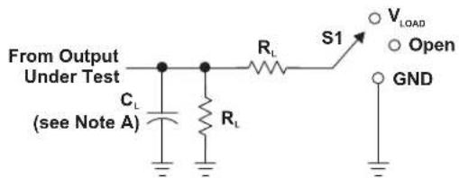
From Output Under Test CL (see Note A) RL RL S1 VLOAD Open GNDLOAD CIRCUIT
| TEST S1 | |
| t_PLH/PHL | Open |
| t_PLZ/PTZL | V_LOAD |
| t_PHZ/PZH | GND |
| V_cc | INPUTS | V_M | V_LOAD | C_L | R_L | V_A | |
| V_I | t_i/t_f | ||||||
| 1.8 V 0.15 V_± | V_cc | ≤2 ns | V_cc/2 | 2 × V_cc | 30 pF | 1 kΩ | 0.15 V |
| 2.5 V 0.2 V_± | V_cc | ≤2 ns | V_cc/2 | 2 × V_cc | 30 pF | 500 Ω | 0.15 V |
| 3.3 V 0.3 V_± | 3 V | ≤2.5 ns | 1.5 V | 6 V | 50 pF | 500 Ω | 0.3 V |
| 5 V 0.5 V_± | V_cc | ≤2.5 ns | V_cc/2 | 2 × V_cc | 50 pF | 500 Ω | 0.3 V |
text_image
Input V_M t_W V_M 0 V VOLTAGE WAVEFORMS PULSE DURATION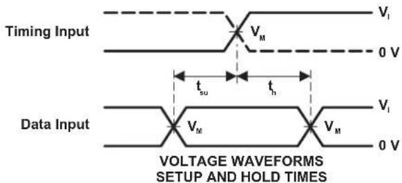
text_image
Timing Input V_M 0 V t_{su} t_h Data Input V_M V_M 0 V VOLTAGE WAVEFORMS SETUP AND HOLD TIMES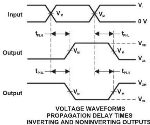
text_image
Input V_M V_M 0 V t_PLH t_PHL Output V_M V_M V_OH V_OL t_PHL t_PLH Output V_M V_M V_OH V_OL VOLT VOLT VOLT VOLT VOLT VOLT VOLT VOLT VOLT VOLT VOLT VOLT VOLT VOLT VOLT VOLT VOLT VOLT VOLT VOLT VOLT VOLT VOLT VOLT VOLT VOLT VOLT VOLT VOLT VOLT
text_image
Output Control V_M V_M 0 V t_PZL t_PLZ Output Waveform 1 S1 at V_LOAD / 2 (see Note B) V_LOAD/V_LOAD V_OL V_OL t_PZH t_PHZ Output Waveform 2 S1 at GND (see Note B) V_M V_OH V_OH ~0 V VOLT V_Λ V_OUT V_Λ V_PHZ V_PHZ V_PHZ V_PHZ V_PHZ V_PHZ V_PHZ V_PHZ V_PHZ V_PHZ V_PHZ V_PHZ V_PHZ V_PHZ V_PHZ V_PHZ V_PHZ V_PHZ V_PHZ V_PHZ V_PHZ V_PHZ V_PHZ V_PHZ V_PHZ V_PNZNOTES: A. C includes probe and jig capacitance.
B. Waveform 1 is for an output with internal conditions such that the output is low, except when disabled by the output control. Waveform 2 is for an output with internal conditions such that the output is high, except when disabled by the output control.
C. All input pulses are supplied by generators having the following characteristics: PRR ≤ 10 MHz, Z_0 = 50 .
D. The outputs are measured one at a time, with one transition per measurement.
E. t_PLZ and t_PHZ are the same as t_ds
F. t_PZL and t_PZH are the same as t_en
G. t_PLH and t_PHL are the same as t_pd
H. All parameters and waveforms are not applicable to all devices.
Figure3. LoadCircuit and Voltage Waveforms
8DetailedDescription
8.1Overview
ThistripleSchmitt-triggerbufferisdesignedfor1.65-Vto5.5-VV CC operation.TheSN74LVC3G17device contains three buffers and perform the Boolean function Y=A. The device functions as three independent buffers but, because of Schmittaction, it may have different input threshold levels for positive going (V negative-going (V _T- ) signals. This device is fully specified for partial-power-down applications using circuitry disable the output, preventing damaging current back flow through the device when it is powered down. NanoFree™packagetechnology is a major breakthrough in C packaging concepts, using the dieasthe package.
8.2FunctionalBlockDiagram
text_image
1A 1Y¹ 2A 2Y³ 3A 3Y⁶ 7 5 28.3FeatureDescription
SN74LVC3G17isavailableinNanoFreepackage.NanoFreeisamajorbreakthroughinICpackagingconcepts, itisabarediepackagedevelopedforapplicationsthatrequirethesmallestpossiblepackage.Thedevice supports5-VV CC Operation.AllInputsacceptvoltagesupto5.5V.±24-mAOutputDriveat3.3V.Themaximum timepropagationdelay(t pd)is5.4nsat3.3V.LowPowerConsumption,10-μAMaxl CC.Typicaloutputground bounce(V OLP)andOutputV OH Undershoot(V OHV).Thisdeviceisfullyspecifiedforpartial-powerdown applicationsusingI off.TheI off featureensuresthatdamagingcurrentwillnotbackflowthroughthedevicewhenit ispowereddown.TheSN74LVC3G17devicehasisolationduringpoweroff.I off supportsliveinsertion,partial-power-downmodeandbackdriveprotection.Thedeviceislatch-upresistantwith100mAexceedingtheJESD 78standard,classII,providingprotectionfromdestructionduetolatch-up.Thisdeviceisprotectedagainst electrostaticdischarge.ItistestedperJESD22using2000-Vhuman-bodymodel(A114-B),200-Vmachine model(A115-A),and1000-Vcharged-devicemodel(C101).
8.4DeviceFunctionalModes
Table1liststhefunctionalmodesoftheSN74LVC3G17.
Table1.FunctionTable
| INPUTA | OUTPUTY |
| H | H |
| L | L |
9ApplicationandImplementation
NOTE
InformationinthefollowingapplicationssectionsisnotpartoftheTlcomponent specification,andTldoesnotwarrantitsaccuracyorcompleteness.TI'scustomersare responsiblefordeterminingsuitabilityofcomponentsfortheirpurposes.Customersshould validateandtesttheirdesignimplementationtoconfirmsystemfunctionality.
9.1 Application Information
TheSN74LVC3G17devicecontainsthreebuffersandperformstheBooleanfunctionY=A.Thedevicefunctionsasthreeindependentbuffers,butbecauseofSchmittaction,itmayhavedifferentinputthresholdlevelsforpositive-going(V T+ )andnegative-going(V T- )signals.Inthisapplication,theengineerchoosestousejustasingleSchmittTriggerbuffer.Inthiscase,theothertwoinputsshouldbetiedtoVCCorGND.
9.2 Typical Application

text_image
3 V SN74LVC3G17 1A 1Y GND VCC 2A 2Y 3A 3Y Device 3 VFigure4.DevicePowerButtonCircuit
9.2.1 DesignRequirements
This device uses CMOS technology and has balanced output drive. Careshould betakento avoid bus contention because it can drive current that would exceed maximum limits. Output scan be combined to produce higher drive but the high drivewill also create faster edges into light loadssorouting and load conditions should be considered to prevent ringing.
9.2.2 Detailed Design Procedure
- Recommended Input Conditions:
-Forspecifiedhighandlowlevels,see(V IH andV IL )inRecommendedOperatingConditionstable.
-Inputsareovervoltagetolerantallowingthemtogoashighas5.5VatanyvalidV cc-
- RecommendOutputConditions:
-Loadcurrentsshouldnotexceed50mAperoutputand100mAtotalforthepart.
–Seriesresistorsontheoutputmaybeusediftheuserdesirestoslowtheoutputedgesignalorlimitthe outputcurrent.
TypicalApplication(continued)
9.2.3 ApplicationCurves
line
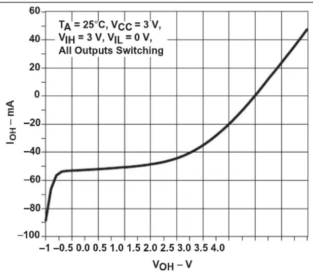
| VOH - V | IOH - mA | | ------- | -------- | | -1.0 | -90 | | -0.5 | -60 | | 0.0 | -55 | | 0.5 | -55 | | 1.0 | -55 | | 1.5 | -55 | | 2.0 | -55 | | 2.5 | -50 | | 3.0 | -40 | | 3.5 | -20 | | 4.0 | 0 | | 4.5 | 20 | | 5.0 | 40 | | 5.5 | 60 |Figure5. OutputCurrentDrive vs HIGH-levelOutputVoltage

line
| VOL - V | IOL - mA | | ------- | -------- | | -0.2 | -20 | | 0.0 | 0 | | 0.2 | 20 | | 0.4 | 40 | | 0.6 | 60 | | 0.8 | 80 | | 1.0 | 100 | | 1.2 | 120 | | 1.4 | 140 | | 1.6 | 160 | | 1.8 | 180 | | 2.0 | 200 | | 2.2 | 220 | | 2.4 | 240 | | 2.6 | 260 | | 2.8 | 280 | | 3.0 | 300 | | 3.2 | 320 | | 3.4 | 340 | | 3.6 | 360 | | 3.8 | 380 | | 4.0 | 400 | | 4.2 | 420 | | 4.4 | 440 | | 4.6 | 460 | | 4.8 | 480 | | 5.0 | 500 | | 5.2 | 520 | | 5.4 | 540 | | 5.6 | 560 | | 5.8 | 580 | | 6.0 | 600 | | 6.2 | 620 | | 6.4 | 640 | | 6.6 | 660 | | 6.8 | 680 | | 7.0 | 700 | | 7.2 | 720 | | 7.4 | 740 | | 7.6 | 760 | | 7.8 | 780 | | 8.0 | 800 | | 8.2 | 820 | | 8.4 | 840 | | 8.6 | 860 | | 8.8 | 880 | | 9.0 | 900 | | 9.2 | 920 | | 9.4 | 940 | | 9.6 | 960 | | 9.8 | 980 | | 10.0 | 100 |Figure6. OutputCurrentDrive vsLOW-levelOutputVoltage
10PowerSupplyRecommendations
The powersupply can be any voltage between the minimum and maximum supply voltage rating located in the Absolute Maximum Rating stable.
EachV CC terminalshouldhaveagoodbypasscapacitortopreventpowerdisturbance.Fordeviceswithasingle supply,a0.1-μFcapacitorisrecommended.IftherearemultipleV CC terminalsthen0.01-μFor0.022-μF capacitorsarerecommendedforeachpowerterminal.Itisoktoparallelmultiplebypasscapacitorstoreject differentfrequenciesofnoise.Multiplebypasscapacitorsmaybeparalleledtorejectdifferentfrequenciesof noise.Thebypasscapacitorshouldbeinstalledasclosetothepowerterminalaspossibleforthebestresults.
11Layout
11.1 LayoutGuidelines
When using multiple bit logic devices, inputs should not float. In many cases, functions or parts of functions of digitallogicdevicesareunused. Some examples are when only two input sof atriple-input AND gate are used, or when only 3 of the 4-buffer gates are used. Such input pin should not be left unconnected because the undefined voltages at the outside connections result in undefined operational states.
Specified in Figure 7 are rules that must be observed under all circumstances. All unused inputs of digital logic devices must be connected to a high or low bias to prevent them from floating. The logic level that should be applied to any particular unused input depends on the function of the device. Generally they will be tied to GND or V_CC , whichever makes moresense or is more convenient.
11.2LayoutExample

text_image
VCC Unused Input Input Output Output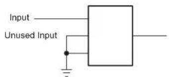
text_image
Input Unused InputFigure7.LayoutDiagram
12DeviceandDocumentationSupport
12.1 DocumentationSupport
12.1.1 Related Documentation
Forrelateddocumentation,seethefollowing: ImplicationsofSloworFloatingCMOSInputs,SCBA004
12.2 Community Resources
The following links connect to TI community resources. Linked contents are provided "ASIS" by the respective contributors. They do not constitute TI specifications and do not necessarily reflect TI's views; see TI's Terms of Use.
TI E2E™ Online Community TI's Engineer-to-Engineer (E2E) Community. Created to foster collaboration amongengineers.Ate2e.ti.com,youcanaskquestions,shareknowledge,exploreideasandhelp solveproblemswithfellowengineers.
Design Support TI's Design Support Quickly find helpful E2E forums along with design support tools and contactinformationfortechnicalsupport.
12.3 Trademarks
E2EisatrademarkofTexasInstruments. Blu-rayisaregisteredtrademarkofBlu-rayDiscAssociation. NanoFreeisatrademarkofTexasInstruments. Allothertrademarksarethepropertyoftheirrespectiveowners.
12.4ElectrostaticDischargeCaution

These devices have limited built-in ESD protection. The leads should be shorted together or the device placed in conductive foam duringstorageorhandlingtopreventelectrostaticdamagetotheMOSgates.
12.5Glossary
SLYZ022—TIGlossary. This glossary lists and explain terms, acronyms, and definitions.
13Mechanical, Packaging, and Orderable Information
The following pages include mechanical packaging and orderable information. This information is most current data available for the designated devices. This data is subject to changewithout notice and revision of this document. For browser-based version of this datasheet, referto the left hand navigation.

TEXAS INSTRUMENTS
www.ti.com
PACKAGE OPTION ADDENDUM
29-Jan-2021
PACKAGING INFORMATION
| Orderable Device Status(1) | Package Type | Package Drawing | Pins | Package Qty | Eco Plan(2) | Lead finish/ Ball material(6) | MSL Peak Temp(3) | Op Temp (°C) | Device Marking(4-5) | Samples | |
| SN74LVC3G17DCTR ACTIVE SM8 DCT 8 3000 RoHS & Green NIPDAU Level-1-260C-UNLIM -40 to 125 C17 | Samples | ||||||||||
| SN74LVC3G17DCTRE4 ACTIVE SM8 DCT 8 3000 RoHS & Green NIPDAU Level-1-260C-UNLIM -40 to 125 C17 | Samples | ||||||||||
| SN74LVC3G17DCTRG4 ACTIVE SM8 DCT 8 3000 RoHS & Green NIPDAU Level-1-260C-UNLIM -40 to 125 C17 | Samples | ||||||||||
| SN74LVC3G17DCUR | ACTIVE | VSSOP | DCU | 8 | 3000 | RoHS & Green | NIPDAU | SN | Level-1-260C-UNLIM | -40 to 125 | (17, C17J, C17Q, C17R)CZ | Samples |
| SN74LVC3G17DCURG4 | ACTIVE | VSSOP | DCU | 8 | 3000 | RoHS & Green | NIPDAU | Level-1-260C-UNLIM | -40 to 125 | C17R | Samples |
| SN74LVC3G17YZPR | ACTIVE | DSBGA | YZP | 8 | 3000 | RoHS & Green | SNAGCU | Level-1-260C-UNLIM | -40 to 85 | C7N | Samples |
(1) The marketing status values are defined as follows:
ACTIVE: Product device recommended for new designs.
LIFEBUY: TI has announced that the device will be discontinued, and a lifetime-buy period is in effect.
NRND: Not recommended for new designs. Device is in production to support existing customers, but TI does not recommend using this part in a new design.
PREVIEW: Device has been announced but is not in production. Samples may or may not be available.
OBSOLETE: TI has discontinued the production of the device.
(2) RoHS: TI defines "RoHS" to mean semiconductor products that are compliant with the current EU RoHS requirements for all 10 RoHS substances, including the requirement that RoHS substance do not exceed 0.1% by weight in homogeneous materials. Where designed to be soldered at high temperatures, "RoHS" products are suitable for use in specified lead-free processes. TI may reference these types of products as "Pb-Free".
RoHS Exempt: TI defines "RoHS Exempt" to mean products that contain lead but are compliant with EU RoHS pursuant to a specific EU RoHS exemption.
Green: TI defines "Green" to mean the content of Chlorine (Cl) and Bromine (Br) based flame retardants meet JS709B low halogen requirements of <=1000ppm threshold. Antimony trioxide based flame retardants must also meet the <=1000ppm threshold requirement.
(3) MSL, Peak Temp. - The Moisture Sensitivity Level rating according to the JEDEC industry standard classifications, and peak solder temperature.
(4) There may be additional marking, which relates to the logo, the lot trace code information, or the environmental category on the device.
(5) Multiple Device Markings will be inside parentheses. Only one Device Marking contained in parentheses and separated by a "-" will appear on a device. If a line is indented then it is a continuation of the previous line and the two combined represent the entire Device Marking for that device.

TEXAS INSTRUMENTS
www.ti.com
PACKAGE OPTION ADDENDUM
29-Jan-2021
(6) Lead finish/Ball material - Orderable Devices may have multiple material finish options. Finish options are separated by a vertical ruled line. Lead finish/Ball material values may wrap to two lines if the finish value exceeds the maximum column width.
Important Information and Disclaimer: The information provided on this page represents TI's knowledge and belief as of the date that it is provided. TI bases its knowledge and belief on information provided by third parties, and makes no representation or warranty as to the accuracy of such information. Efforts are underway to better integrate information from third parties. TI has taken and continues to take reasonable steps to provide representative and accurate information but may not have conducted destructive testing or chemical analysis on incoming materials and chemicals. TI and TI suppliers consider certain information to be proprietary, and thus CAS numbers and other limited information may not be available for release.
In no event shall TI's liability arising out of such information exceed the total purchase price of the TI part(s) at issue in this document sold by TI to Customer on an annual basis.
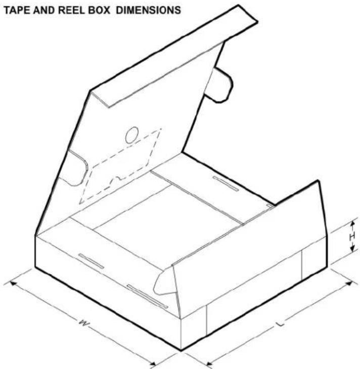
TAPE AND REEL INFORMATION

*All dimensions are nominal
| Device Package | Type | Package Drawing | Pins | SPQ Reel | Diameter (mm) | Reel Width W1 (mm) | A0 (mm) | B0 (mm) | K0 (mm) | P1 (mm) | W (mm) | Pin1 Quadrant |
| SN74LVC3G17DCTR SM8 DCT 8 | 3000 180.0 | 13.0 | 3.35 4.5 1 | 55 4.0 12.0 | Q3 | |||||||
| SN74LVC3G17DCTR SM8 DCT 8 | 3000 177.8 | 12.4 | 3.45 4.4 1 | 45 4.0 12.0 | Q3 | |||||||
| SN74LVC3G17DCUR VSSOP DCU 8 3000 1 | 80.0 8 | 4 2.25 3.3 | 5 1.05 4.0 | 8.0 | Q3 | |||||||
| SN74LVC3G17DCUR VSSOP DCU 8 3000 1 | 78.0 9 | 0 2.25 3.3 | 5 1.05 4.0 | 8.0 | Q3 | |||||||
| SN74LVC3G17DCUR VSSOP DCU 8 3000 1 | 80.0 9 | 0 2.25 3.4 | 1.0 4.0 8.0 | Q3 | ||||||||
| SN74LVC3G17DCUR VSSOP DCU 8 3000 1 | 78.0 9 | 5 2.25 3.3 | 5 1.05 4.0 | 8.0 | Q3 | |||||||
| SN74LVC3G17DCURG4VSSOP DCU 8 3000 | 180.0 | 8.4 2.25 3 | 35 1.05 4.0 | 8.0 | Q3 | |||||||
| SN74LVC3G17YZPR D$BGA YZF | 8 3000 17 | 8.0 | 9.2 1.02 | 2.02 0.63 | 4.0 8.0 Q1 |
text_image
TAPE AND REEL BOX DIMENSIONS W L*All dimensions are nominal
| Device | Package Type | Package Drawing | Pins | SPQ | Length (mm) | Width (mm) | Height (mm) |
| SN74LVC3G17DCTR SM8 DCT 8 3000 182.0 | 182.0 20.0 | ||||||
| SN74LVC3G17DCTR SM8 DCT 8 3000 183.0 | 183.0 20.0 | ||||||
| SN74LVC3G17DCUR VSSOP DCU 8 3000 | 202.0 201.0 28.0 | ||||||
| SN74LVC3G17DCUR VSSOP DCU 8 3000 | 80.0 180.0 18.0 | ||||||
| SN74LVC3G17DCUR VSSOP DCU 8 3000 | 82.0 182.0 20.0 | ||||||
| SN74LVC3G17DCUR VSSOP DCU 8 3000 | 202.0 201.0 28.0 | ||||||
| SN74LVC3G17DCURG4 | VSSOP DCU 8 3000 202.0 201.0 | 28.0 | |||||
| SN74LVC3G17YZPR | DSBGA | YZP | 8 | 3000 | 220.0 | 220.0 | 35.0 |
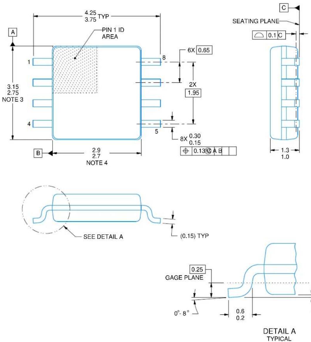
SMALL OUTLINE PACKAGE

text_image
0.25 GAGE PLANE 0°-8° 0.6 0.2 0.1 0.0 DETAIL A TYPICAL4220784/C 06/2021
NOTES:
- All linear dimensions are in millimeters. Dimensions in parenthesis are for reference only. Dimensioning and tolerancing per ASME Y14.5M.
- This drawing is subject to change without notice.
- This dimension does not include mold flash, protrusions, or gate burrs. Mold flash, protrusions, or gate burrs shall not exceed 0.15 mm per side.
- This dimension does not include interlead flash. Interlead flash shall not exceed 0.25 mm per side.
SMALL OUTLINE PACKAGE

text_image
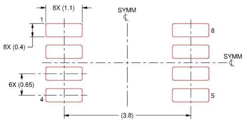
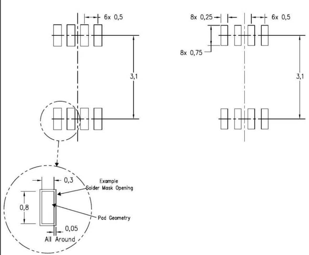
8X (1.1) 1 8X (0.4) 6X (0.65) 4 (3.8) SYMM (80.05) TYP SYMM 5LAND PATTERN EXAMPLE
EXPOSED METAL SHOWN
SCALE:15X

text_image
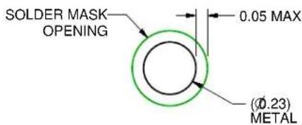
SOLDER MASK OPENING METAL EXPOSED METAL 0.07 MAX ALL AROUNDNON SOLDER MASK
DEFINED

text_image
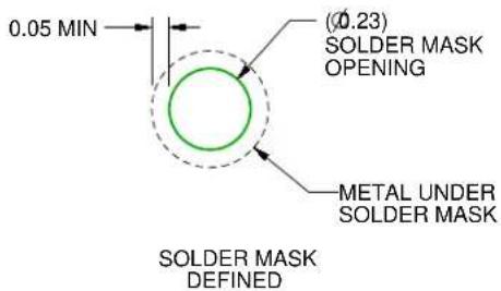
METAL UNDER SOLDER MASK SOLDER MASK OPENING EXPOSED METAL 0.07 MIN ALL AROUNDSOLDER MASK
DEFINED
SOLDER MASK DETAILS
4220784/C 06/2021
NOTES: (continued)
- Publication IPC-7351 may have alternate designs.
- Solder mask tolerances between and around signal pads can vary based on board fabrication site.
SMALL OUTLINE PACKAGE
text_image
8X (1.1) SYMM 1 8X (0.4) 6X (0.65) 4 (3.8) SYMM 8 SYMM 5SOLDER PASTE EXAMPLE
BASED ON 0.125 mm THICK STENCIL
SCALE:15X
4220784/C 06/2021
NOTES: (continued)
- Laser cutting apertures with trapezoidal walls and rounded corners may offer better paste release. IPC-7525 may have alternate design recommendations.
- Board assembly site may have different recommendations for stencil design.
DIE SIZE BALL GRID ARRAY

D: Max = 1.919 mm, Min = 1.858 mm
E: Max = 0.918 mm, Min = 0.857 mm
4223082/A 07/2016
NOTES:
- All linear dimensions are in millimeters. Any dimensions in parenthesis are for reference only. Dimensioning and tolerancing per ASME Y14.5M.
- This drawing is subject to change without notice.
DIE SIZE BALL GRID ARRAY

text_image
8X (Ø.23) (0.5) TYP (0.5) TYP A B C D SYMM SYMMLAND PATTERN EXAMPLE SCALE:40X
text_image
SOLDER MASK OPENING 0.05 MAX (Ø23) METALNON-SOLDER MASK DEFINED (PREFERRED)
text_image
0.05 MIN (0.23) SOLDER MASK OPENING METAL UNDER SOLDER MASK SOLDER MASK DEFINEDSOLDER MASK DETAILS NOT TO SCALE
4223082/A 07/2016
NOTES: (continued)
- Final dimensions may vary due to manufacturing tolerance considerations and also routing constraints. For more information, see Texas Instruments literature number SNVA009 (www.ti.com/lit/snva009).
DIE SIZE BALL GRID ARRAY

text_image
8X (0.25) (0.5) TYP 1 2 (R0.05) TYP (0.5) TYP A B SYMM C METAL TYP D SYMMSOLDER PASTE EXAMPLE BASED ON 0.1 mm THICK STENCIL SCALE:40X
4223082/A 07/2016
NOTES: (continued)
- Laser cutting apertures with trapezoidal walls and rounded corners may offer better paste release.
DCU (R-PDSO-G8)
PLASTIC SMALL-OUTLINE PACKAGE (DIE DOWN)
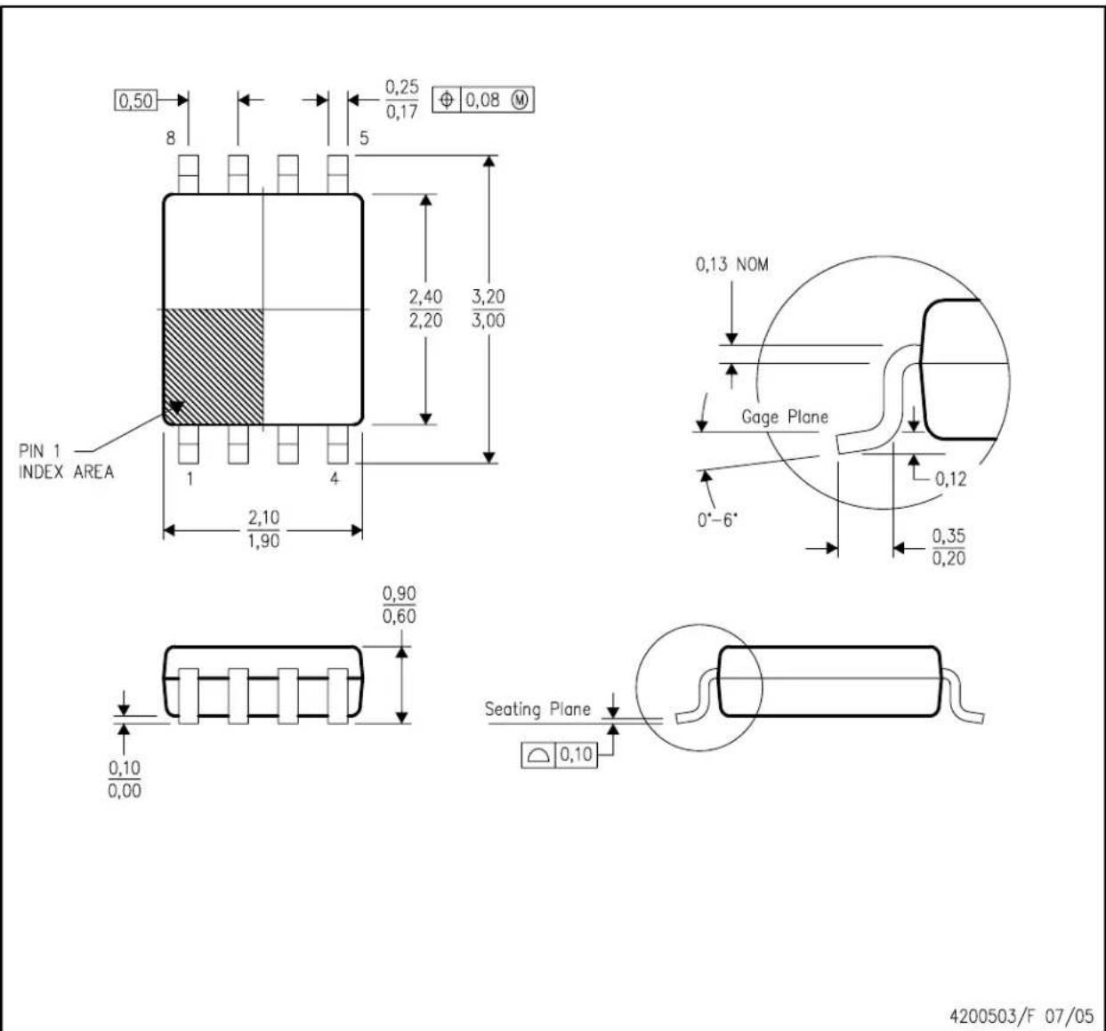
4200503/F 07/05
NOTES: A. All linear dimensions are in millimeters.
B. This drawing is subject to change without notice.
C. Body dimensions do not include mold flash or protrusion. Mold flash and protrusion shall not exceed 0.15 per side.
D. Falls within JEDEC MO-187 variation CA.
DCU (S-PDSO-G8)
PLASTIC SMALL OUTLINE PACKAGE (DIE DOWN)
Example Board Layout (Note C,E)
Example Stencil Design (Note D)
4210064/C 04/12
NOTES: A. All linear dimensions are in millimeters.
B. This drawing is subject to change without notice.
C. Publication IPC-7351 is recommended for alternate designs.
D. Laser cutting apertures with trapezoidal walls and also rounding corners will offer better paste release. Customers should contact their board assembly site for stencil design recommendations. Refer to IPC-7525 for other stencil recommendations.
E. Customers should contact their board fabrication site for solder mask tolerances between and around signal pads.
IMPORTANT NOTICE AND DISCLAIMER
TI PROVIDES TECHNICAL AND RELIABILITY DATA (INCLUDING DATA SHEETS), DESIGN RESOURCES (INCLUDING REFERENCE DESIGNS), APPLICATION OR OTHER DESIGN ADVICE, WEB TOOLS, SAFETY INFORMATION, AND OTHER RESOURCES "AS IS" AND WITH ALL FAULTS, AND DISCLAIMS ALL WARRANTIES, EXPRESS AND IMPLIED, INCLUDING WITHOUT LIMITATION ANY IMPLIED WARRANTIES OF MERCHANTABILITY, FITNESS FOR A PARTICULAR PURPOSE OR NON-INFRINGEMENT OF THIRD PARTY INTELLECTUAL PROPERTY RIGHTS.
These resources are intended for skilled developers designing with TI products. You are solely responsible for (1) selecting the appropriate TI products for your application, (2) designing, validating and testing your application, and (3) ensuring your application meets applicable standards, and any other safety, security, regulatory or other requirements.
These resources are subject to change without notice. TI grants you permission to use these resources only for development of an application that uses the TI products described in the resource. Other reproduction and display of these resources is prohibited. No license is granted to any other TI intellectual property right or to any third party intellectual property right. TI disclaims responsibility for, and you will fully indemnify TI and its representatives against, any claims, damages, costs, losses, and liabilities arising out of your use of these resources.
TI's products are provided subject to TI's Terms of Sale or other applicable terms available either on ti.com or provided in conjunction with such TI products. TI's provision of these resources does not expand or otherwise alter TI's applicable warranties or warranty disclaimers for TI products.
TI objects to and rejects any additional or different terms you may have proposed.
Mailing Address: Texas Instruments, Post Office Box 655303, Dallas, Texas 75265
Copyright © 2022, Texas Instruments Incorporated