CY74FCT573ATSOC - Electronic component TEXAS INSTRUMENTS - Free user manual and instructions
Find the device manual for free CY74FCT573ATSOC TEXAS INSTRUMENTS in PDF.

User questions about CY74FCT573ATSOC TEXAS INSTRUMENTS
0 question about this device. Answer the ones you know or ask your own.
Ask a new question about this device
Download the instructions for your Electronic component in PDF format for free! Find your manual CY74FCT573ATSOC - TEXAS INSTRUMENTS and take your electronic device back in hand. On this page are published all the documents necessary for the use of your device. CY74FCT573ATSOC by TEXAS INSTRUMENTS.
USER MANUAL CY74FCT573ATSOC TEXAS INSTRUMENTS
- Function and Pinout Compatible With FCT and F Logic
- Reduced V_OH (Typically = 3.3 V) Versions of Equivalent FCT Functions
- Edge-Rate Control Circuitry for Significantly Improved Noise Characteristics
-
I_off Supports Partial-Power-Down Mode Operation
• ESD Protection Exceeds JESD 22 -
2000-V Human-Body Model (A114-A)
- 200-V Machine Model (A115-A)
-
1000-V Charged-Device Model (C101)
-
Matched Rise and Fall Times
● Fully Compatible With TTL Input and Output Logic Levels
3-State Outputs
CY54FCT573T
- 32-mA Output Sink Current
- 12-mA Output Source Current
CY74FCT573T
- 64-mA Output Sink Current
- 32-mA Output Source Current
description
CY54FCT573T ... D P A C KAGE
CY74FCT573T ... P, Q, O R S O P A C KAGE
(TOP VIEW)

text_image
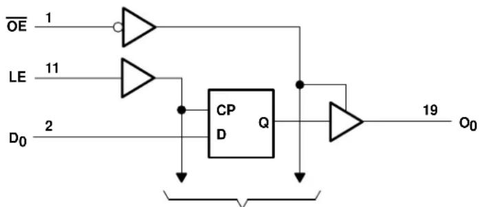
OE 1 20 VCC D0 2 19 O0 D1 3 18 O1 D2 4 17 O2 D3 5 16 O3 D4 6 15 O4 D5 7 14 O5 D6 8 13 O6 D7 9 12 O7 GND 10 11 LEThe 'FCT573T devices consist of eight latches with 3-state outputs for bus-organized applications. When the latch-enable (LE) input is high, the flip-flops appear transparent to the data. Data that meets the required setup times are latched when LE transitions from high to low. Data appears on the bus when the output-enable (OE) input is low. When OE is high, the bus output is in the high-impedance state. In this mode, data can be entered into the latches. The 'FCT573T devices are identical to the 'FCT373T devices, except for the flow-through pinout of the 'FCT573T, which simplifies board design.
These devices are fully specified for partial-power-down applications using I_off . The I_off circuitry disables the outputs, preventing damaging current backflow through the device when it is powered down.

Please be aware that an important notice concerning availability, standard warranty, and use in critical applications of Texas Instruments semiconductor products and disclaimers thereto appears at the end of this data sheet.
PRODUCTION DATA information is current as of publication date. Products conform to specifications per the terms of Texas Instruments standard warranty. Production processing does not necessarily include testing of all parameters.

TEXAS
INSTRUMENTS
POST OFFICE BOX 655303 • DALLAS, TEXAS 75265
Copyright 2001, Texas Instruments Incorporated On products compliant to MIL-PRF-38535, all parameters are tested unless otherwise noted. On all other products, production processing does not necessarily include testing of all parameters.
ORDERING INFORMATION
| T_A | PACKAGE^ | SPEED(ns) | ORDERABLEPART NUMBER | TOP-SIDEMARKING | |
| -40°C to 85°C | QSOP - Q | Tape and reel | 4.7 | CY74FCT573CTQCT | FCT573C |
| SOIC °°SU | Tube 4.7 CY74F | CT573CTSOC | FCT573C | ||
| Tape and reel 4.7 | CY74FCT573CTSOCT | ||||
| DIP - P Tube | 5.2 CY74FCT573 | ATPC CY74FCT573ATPC | |||
| QSOP - Q | Tape and reel | 5.2 | CY74FCT573ATQCT | FCT573A | |
| SOIC °°SU | Tube 5.2 CY74F | CT573ATSOC | FCT573A | ||
| Tape and reel 5.2 | CY74FCT573ATSOCT | ||||
| QSOP - Q | Tape and reel | 8 | CY74FCT573TQCT | FCT573 | |
| SOIC °°SU | Tube 8 CY74FC | T573TSOC | FCT573 | ||
| Tape and reel 8 | CY74FCT573TSOCT | ||||
| -55°C to 125°C | CDIP - D | Tube | 8.5 | CY54FCT573ATLMB | |
† Package drawings, standard packing quantities, thermal data, symbolization, and PCB design guidelines are available at www.ti.com/sc/package.
FUNCTION TABLE
| INPUTS | OUTPUTO | ||
| OE | LE | D | |
| L H | H | H | |
| L H | L | L | |
| L L | X | Q 0 | |
| H | X | X | Z |
H = High logic level, L = Low logic level,
X = Don't care, Z = High-impedance state,
Q_n= Previous state of flip flops ( Q_n-1 )
logic diagram (positive logic)
flowchart
graph TD
    OE["OE"] -->|1| NOR1["NOT"]
    LE["LE"] -->|11| NOR2["NOT"]
    D0["D0"] -->|2| DFF1["CP D Q"]
    NOR1 --> AND1["AND"]
    NOR2 --> AND2["AND"]
    DFF1 --> OR1["OR"]
    OR1 --> O0["O0"]
    DFF1 --> OR2["OR"]
    OR2 --> 19["19"]
    style DFF1 fill:#f9f,stroke:#333
    style OR1 fill:#ccf,stroke:#333
    style OR2 fill:#ccf,stroke:#333
To Seven Other Channels
absolute maximum rating over operating free-air temperature range (unless otherwise noted)†
Supply voltage range to ground potential -0.5 V to 7 V
DC input voltage range -0.5 V to 7 V
DC output voltage range -0.5 V to 7 V
DC output current (maximum sink current/pin) 120 mA
Package thermal impedance, _JA (see Note 1): P package 69°C/W
Q package 68°C/W
SO package 58°C/W
Ambient temperature range with power applied, T_A –65°C to 135°C
Storage temperature range, T_stg -65^ to 150^
Stresses beyond those listed under "absolute maximum ratings" may cause permanent damage to the device. These are stress ratings only, and functional operation of the device at these or any other conditions beyond those indicated under "recommended operating conditions" is not implied.
Exposure to absolute-maximum-rated conditions for extended periods may affect device reliability.
NOTE 1: The package thermal impedance is calculated in accordance with JESD 51-7.
recommended operating conditions (see Note 2)
| CY54FCT573T | CY74FCT573T | UNIT | ||||||
| MIN | NOM | MAX | MIN | NOM | MAX | |||
| V_CC | Supply voltage | 4.5 | 5 | 5.5 | 4.75 | 5 | 5.25 | V |
| V_IH | High-level input voltage | 2 | 2 | V | ||||
| V_IL | Low-level input voltage | 0.8 | 0.8 | V | ||||
| I_OH | High-level output current | -12 | -32 | mA | ||||
| I_OL | Low-level output current | 32 | 64 | mA | ||||
| T_A | Operating free-air temperature | -55 | 125 | -40 | 85 | °C | ||
NOTE 2: All unused inputs of the device must be held at V_CC or GND to ensure proper device operation.
electrical characteristics over recommended operating free-air temperature range (unless otherwise noted)
| PARAMETER | TEST CONDITIONS | CY54FCT573T CY7 | FCT573T | UNIT | |||||
| MIN TYP | MAX | MIN TYP | MAX | ||||||
| V_IK | V_CC = 4.5 V, I | IN = -18 mA | -0.7 | -1.2 | V | ||||
| V_CC = 4.75 V, I | IN = -18 mA | -0.7 | -1.2 | ||||||
| V_OH | V_CC = 4.5 V, I | OH = -12 mA 2.4 3.3 | V | ||||||
| V_CC = 4.75 V | IOH = -32 mA 2 | ||||||||
| IOH = -15 mA 2.4 3.3 | |||||||||
| V_OL | V_CC = 4.5 V, I | OL = 32 mA 0.3 0.55 | V | ||||||
| V_CC = 4.75 V, I | OL = 64 mA 0.3 0.55 | ||||||||
| V_hys | All inputs | 0.2 | 0.2 | V | |||||
| I_1 | V_CC = 5.5 V, V | IN = V_CC | 5 | A | |||||
| V_CC = 5.25 V, V | IN = V_CC | ||||||||
| I_TH | V_CC = 5.5 V, V | IN = 2.7 V | ±1 | A | |||||
| V_CC = 5.25 V, V | IN = 2.7 V | ||||||||
| I_TL | V_CC = 5.5 V, V | IN = 0.5 V | ±1 | A | |||||
| V_CC = 5.25 V, V | IN = 0.5 V | ||||||||
| I_OZH | V_CC = 5.5 V, V | OUT = 2.7 V | 10 | A | |||||
| V_CC = 5.25 V, V | OUT = 2.7 V | ||||||||
| I_OZL | V_CC = 5.5 V, V | OUT = 0.5 V | -10 | A | |||||
| V_CC = 5.25 V, V | OUT = 0.5 V | ||||||||
| I_OS^ | V_CC = 5.5 V, V | OUT = 0 V | -60 | -120 | -225 | mA | |||
| V_CC = 5.25 V, V | OUT = 0 V | -60 | -120 | ||||||
| I_off | V_CC = 0 V, | V_OUT = 4.5 V | ±1 | A | |||||
| I_CC | V_CC = 5.5 V, V | IN ≤ 0.2 V, VIN ≥ V_CC - 0.2 V | 0.1 | 0.2 | mA | ||||
| V_CC = 5.25 V, V | IN ≤ 0.2 V, VIN ≥ V_CC - 0.2 V | ||||||||
| I_CC | V_CC = 5.5 V, V_IN = 3.4 V, f_1 = 0, Outputs open | 0.5 | 2 | mA | |||||
| V_CC = 5.25 V, V_IN = 3.4 V, f_1 = 0, Outputs open | 0.5 | 2 | |||||||
| I_CCD^ | V_CC = 5.5 V, Outputs open, One input switching at 50% duty cycle, = GND, V_IN ≤ 0.2 V or V_IN ≥ V_CC - 0.2 V | 0.06 | 0.12 | mA/MHz | |||||
| V_CC = 5.25 V, Outputs open, One input switching at 50% duty cycle, = GND, V_IN ≤ 0.2 V or V_IN ≥ V_CC - 0.2 V | |||||||||
Typical values are at V_CC = 5 V , T_A = 25^ .
Not more than one output should be shorted at a time. Duration of short should not exceed one second. The use of high-speed test apparatus and/or sample-and-hold techniques are preferable to minimize internal chip heating and more accurately reflect operational values. Otherwise, prolonged shorting of a high output can raise the chip temperature well above normal and cause invalid readings in other parametric tests. In any sequence of parameter tests, IOS tests should be performed last.
§ Per TTL-driven input ( V_IN = 3.4 V); all other inputs at V_CC or GND
¶ This parameter is derived for use in total power-supply calculations.
electrical characteristics over recommended operating free-air temperature range (unless otherwise noted) (continued)
| PARAMETER | TEST CONDITIONS | CY54FCT573T CY7 | 4FCT573T | UNIT | ||||
| MIN TYP † MAX | MIN TYP † MAX | |||||||
| I_C^\# | V_CC=5.5V, E=GND, LE=V_CC | One bit switching at f1=10 MHz at 50% duty cycle | V_IN≤ 0.2V or V_IN≥ V_CC-0.2V | 0.7 1.4 | mA | |||
| V_IN=3.4V or GND 1 | 2.4 | |||||||
| Eight bits switching at f1=2.5 MHz at 50% duty cycle | V_IN≤ 0.2V or V_IN≥ V_CC-0.2V | 1.3 2.6 || | ||||||
| V_IN=3.4V or GND 3.3 10.6 | || | |||||||
| V_CC=5.25V, E=GND, LE=V_CC | One bit switching at f1=10 MHz at 50% duty cycle | V_IN≤ 0.2V or V_IN≥ V_CC-0.2V | 0.7 1.4 | |||||
| V_IN=3.4V or GND 1 | 2.4 | |||||||
| Eight bits switching at f1=2.5 MHz at 50% duty cycle | V_IN≤ 0.2V or V_IN≥ V_CC-0.2V | 1.3 2.6 || | ||||||
| V_IN=3.4V or GND 3.3 10.6 | || | |||||||
| C_1 | 6 10 6 10 pF | |||||||
| C_0 | 8 12 8 12 pF | |||||||
Typical values are at V_CC = 5 V, T_A = 25^.
# I_C = I_CC + I_CC · D_H · N_T + I_CCD(f_0/2 + f_1 · N_1)
Where
I_C = Total supply current
I_CC = Power - supply current with CMOS input levels
I_CC = Power-supply current for a TTL high input (V_IN = 3.4V)
D_H = Duty cycle for TTL inputs high
N_T = Number of TTL inputs at D_H
I_CCD = Dynamic current caused by an input transition pair (HLH or LHL)
f_0 = Clock frequency for registered devices, otherwise zero
f1 = Input signal frequency
N_1 = Number of inputs changing at f_1
All currents are in milliamperes and all frequencies are in megahertz.
|| Values for these conditions are examples of the I_CC formula.
timing requirements over recommended operating free-air temperature range (unless otherwise noted) (see Figure 1)
| CY54FCT573T | Y54FCT573AT | UNIT | ||
| MIN MAX MIN | MAX | |||
| t_w | Pulse duration, LE high | 6 | 6 | ns |
| t_su | Setup time, data before LE^ | 2 | 2 | ns |
| t_h | Hold time, data after LE^ | 1.5 | 1.5 | ns |
timing requirements over recommended operating free-air temperature range (unless otherwise noted) (see Figure 1)
| CY74FCT573T | CY74FCT573AT | CY74FCT573CT | UNIT | ||
| MIN MAX MIN | MAX MIN MAX | ||||
| t_w | Pulse duration, LE high | 6 | 5 | 5 | ns |
| t_su | Setup time, data before LE | 2 | 2 | 2 | ns |
| t_h | Hold time, data after LE | 1.5 | 1.5 | 1.5 | ns |
switching characteristics over operating free-air temperature range (see Figure 1)
| PARAMETER | FROM TO(INPUT) (OUTPUT) | CY54FCT573AT | UNIT | |
| MIN MAX | ||||
| t_PLH | D | O | 1.5 5.6 | ns |
| t_PHL | 1.5 5.6 | |||
| t_PLH | LE | O | 2 9.8 | ns |
| t_PHL | 2 9.8 | |||
| t_PZH | O | 1.5 7.5 | ns | |
| t_PZL | 1.5 7.5 | |||
| t_PHZ | O | 1.5 6.5 | ns | |
| t_PLZ | 1.5 6.5 |
switching characteristics over operating free-air temperature range (see Figure 1)
| PARAMETER | FROM TO(INPUT) (OUTPUT) | CY74FCT573T | CY74FCT573AT CY74FCT573CT | UNIT | ||
| MIN MAX MIN | MAX MIN MAX | |||||
| t_PLH | D | O | 1.5 8 1.5 5.2 | 1.5 4.7 | ns | |
| t_PHL | 1.5 8 1.5 5.2 | 1.5 4.7 | ||||
| t_PLH | LE | O | 2 13 | 2 8.5 | 2 5.5 | ns |
| t_PHL | 2 13 | 2 8.5 | 2 5.5 | |||
| t_PZH | O | 1.5 12 | 1.5 6.5 1.5 5.5 | ns | ||
| t_PZL | 1.5 12 | 1.5 6.5 1.5 5.5 | ||||
| t_PHZ | O | 1.5 7.5 1.5 5.5 | 1.5 5 | ns | ||
| t_PLZ | 1.5 7.5 1.5 5.5 | 1.5 5 | ||||
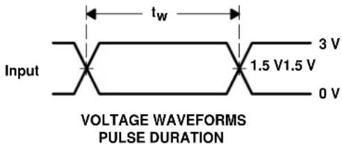
PARAMETER MEASUREMENT INFORMATION

text_image
From Output Under Test CL = 50 pF (see Note A) Test Point 500 ΩLOAD CIRCUIT FOR TOTEM-POLE OUTPUTS

text_image
From Output Under Test C_L = 50 pF (see Note A) 500 Ω 500 Ω S1 7 V Open GNDLOAD CIRCUIT FOR 3-STATE OUTPUTS
| TEST S1 | |
| t_PLH/t_PHL | Open |
| t_PLZ/t_PZL | 7 V |
| t_PHZ/t_PZH | Open |
text_image
Input VOLTAGE WAVEFORMS PULSE DURATION 3 V 1.5 V 1.5 V 0 V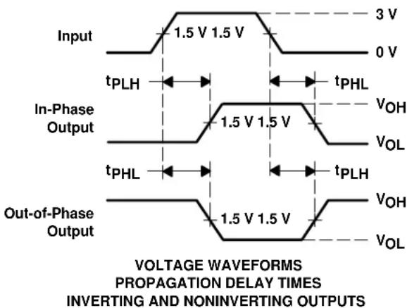
text_image
Input 1.5 V 1.5 V 3 V 0 V tPLH tPHL In-Phase Output 1.5 V 1.5 V VOH VOL tPHL tPLH Out-of-Phase Output 1.5 V 1.5 V VOH VOL VOLTAGE WAVEFORMS PROPAGATION DELAY TIMES INVERTING AND NONINVERTING OUTPUTS
text_image
Timing Input 1.5 V 3 V 0 V tsu th Data Input 1.5 V 1.5 V 3 V 0 V VOLTAGE WAVEFORMS SETUP AND HOLD TIMES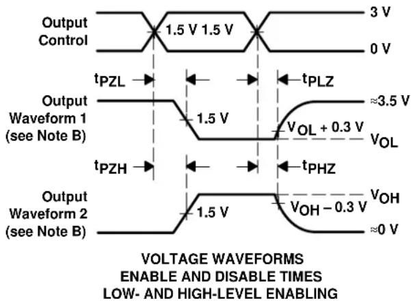
other
| Waveform | Pulse Width (V) | |----------|-----------------| | Output Control | 3 V | | Output Waveform 1 (see Note B) | 1.5 V | | Output Waveform 2 (see Note B) | 1.5 V | | Voltage Waveforms Enable and Disable Times Low- and High-Level Enabling | 3.5 V | | Voltage Waveforms Enable and Disable Times Low- and High-Level Enabling | 0 V | | Voltage Waveforms Enable and Disable Times Low- and High-Level Enabling | -0.3 V |NOTES: A. C L includes probe and jig capacitance.
B. Waveform 1 is for an output with internal conditions such that the output is low except when disabled by the output control.
Waveform 2 is for an output with internal conditions such that the output is high except when disabled by the output control.
C. The outputs are measured one at a time with one input transition per measurement.
Figure 1. Load Circuit and Voltage Waveforms
PACKAGING INFORMATION
| Orderable Device Status(1) | Package Type | Package Drawing | Pins | Package Qty | Eco Plan(2) | Lead finish/ Ball material(6) | MSL Peak Temp(3) | Op Temp (°C) | Device Marking(4/5) | Samples | |
| 5962-9223801MRA ACTIVE CDIP J 20 1 Non-RoHS | & Green | SNPB N / A for Pkg Type -55 to 125 5962-9223801MR | A | Samples | |||||||
| 5962-9223802M2A ACTIVE LCCC FK 20 1 Non-RoHS | & Green | SNPB N / A for Pkg Type -55 to 125 5962- | 9223802M2ACY54FCT573ATLMB | Samples | |||||||
| CY54FCT573ATLMB ACTIVE LCCC FK 20 1 Non-RoHS | & Green | SNPB N / A for Pkg Type -55 to 125 5962- | 9223802M2ACY54FCT573ATLMB | Samples | |||||||
| CY74FCT573ATPC ACTIVE PDIP N 20 20 RoHS & | Non-Green | NIPDAU | N / A for Pkg Type | -40 to 85 | CY74FCT573ATPC | Samples | |||||
| CY74FCT573ATQCT | ACTIVE | SSOP | DBQ | 20 | 2500 | RoHS & Green | NIPDAU | Level-2-260C-1 YEAR | -40 to 85 | FCT573A | Samples |
| CY74FCT573ATSOC | ACTIVE | SOIC | DW | 20 | 25 | RoHS & Green | NIPDAU | Level-1-260C-UNLIM | -40 to 85 | FCT573A | Samples |
| CY74FCT573ATSOCT | ACTIVE | SOIC | DW | 20 | 2000 | RoHS & Green | NIPDAU | Level-1-260C-UNLIM | -40 to 85 | FCT573A | Samples |
| CY74FCT573CTQCT | ACTIVE | SSOP | DBQ | 20 | 2500 | RoHS & Green | NIPDAU | Level-2-260C-1 YEAR | -40 to 85 | FCT573C | Samples |
| CY74FCT573CTQCTG4 | ACTIVE | SSOP | DBQ | 20 | 2500 | RoHS & Green | NIPDAU | Level-2-260C-1 YEAR | -40 to 85 | FCT573C | Samples |
| CY74FCT573CTSOC | ACTIVE | SOIC | DW | 20 | 25 | RoHS & Green | NIPDAU | Level-1-260C-UNLIM | -40 to 85 | FCT573C | Samples |
| CY74FCT573CTSOCG4 | ACTIVE | SOIC | DW | 20 | 25 | RoHS & Green | NIPDAU | Level-1-260C-UNLIM | -40 to 85 | FCT573C | Samples |
| CY74FCT573TQCT | ACTIVE | SSOP | DBQ | 20 | 2500 | RoHS & Green | NIPDAU | Level-2-260C-1 YEAR | -40 to 85 | FCT573 | Samples |
| CY74FCT573TSOC | ACTIVE | SOIC | DW | 20 | 25 | RoHS & Green | NIPDAU | Level-1-260C-UNLIM | -40 to 85 | FCT573 | Samples |
(1) The marketing status values are defined as follows:
ACTIVE: Product device recommended for new designs.
LIFEBUY: TI has announced that the device will be discontinued, and a lifetime-buy period is in effect.
NRND: Not recommended for new designs. Device is in production to support existing customers, but TI does not recommend using this part in a new design.
PREVIEW: Device has been announced but is not in production. Samples may or may not be available.
OBSOLETE: TI has discontinued the production of the device.

TEXAS INSTRUMENTS
www.ti.com
PACKAGE OPTION ADDENDUM
9-Mar-2021
(2) RoHS: TI defines "RoHS" to mean semiconductor products that are compliant with the current EU RoHS requirements for all 10 RoHS substances, including the requirement that RoHS substance do not exceed 0.1% by weight in homogeneous materials. Where designed to be soldered at high temperatures, "RoHS" products are suitable for use in specified lead-free processes. TI may reference these types of products as "Pb-Free".
RoHS Exempt: TI defines "RoHS Exempt" to mean products that contain lead but are compliant with EU RoHS pursuant to a specific EU RoHS exemption.
Green: TI defines "Green" to mean the content of Chlorine (Cl) and Bromine (Br) based flame retardants meet JS709B low halogen requirements of <=1000ppm threshold. Antimony trioxide based flame retardants must also meet the <=1000ppm threshold requirement.
(3) MSL, Peak Temp. - The Moisture Sensitivity Level rating according to the JEDEC industry standard classifications, and peak solder temperature.
(4) There may be additional marking, which relates to the logo, the lot trace code information, or the environmental category on the device.
(5) Multiple Device Markings will be inside parentheses. Only one Device Marking contained in parentheses and separated by a "\~" will appear on a device. If a line is indented then it is a continuation of the previous line and the two combined represent the entire Device Marking for that device.
(6) Lead finish/Ball material - Orderable Devices may have multiple material finish options. Finish options are separated by a vertical ruled line. Lead finish/Ball material values may wrap to two lines if the finish value exceeds the maximum column width.
Important Information and Disclaimer: The information provided on this page represents TI's knowledge and belief as of the date that it is provided. TI bases its knowledge and belief on information provided by third parties, and makes no representation or warranty as to the accuracy of such information. Efforts are underway to better integrate information from third parties. TI has taken and continues to take reasonable steps to provide representative and accurate information but may not have conducted destructive testing or chemical analysis on incoming materials and chemicals. TI and TI suppliers consider certain information to be proprietary, and thus CAS numbers and other limited information may not be available for release.
In no event shall TI's liability arising out of such information exceed the total purchase price of the TI part(s) at issue in this document sold by TI to Customer on an annual basis.
TAPE AND REEL INFORMATION

*All dimensions are nominal
| Device Package | Type | Package Drawing | Pins | SPQ Reel | Diameter (mm) | Reel Width W1 (mm) | A0 (mm) | B0 (mm) | K0 (mm) | P1 (mm) | W (mm) | Pin1 Quadrant |
| CY74FCT573ATQCT SSOP DBQ | 20 2500 33 | 30.0 16 | 4 6.5 9.0 | 2.1 8.0 16 | 0 Q1 | |||||||
| CY74FCT573ATSOCT SOIC DW 20 | 20 2000 33 | 0.0 24 | 4 10.8 13.8 | 2.7 12.0 | 24.0 Q1 | |||||||
| CY74FCT573CTQCT SSOP DBQ | 20 2500 33 | 0.0 16 | 4 6.5 9.0 | 2.1 8.0 16 | 0 Q1 | |||||||
| CY74FCT573TQCT SSOP DBQ | 20 2500 33 | 0.0 16 | 4 6.5 9.0 | 2.1 8.0 16 | 0 Q1 |

text_image
TAPE AND REEL BOX DIMENSIONS W L*All dimensions are nominal
| Device | Package Type | Package Drawing | Pins | SPQ | Length (mm) | Width (mm) | Height (mm) |
| CY74FCT573ATQCT SS | OP DBQ 20 2500 8 | 53.0 449.0 35.0 | |||||
| CY74FCT573ATSOCT SOIC | DW 20 2000 36 | 7.0 367.0 45.0 | |||||
| CY74FCT573CTQCT SS | OP DBQ 20 2500 8 | 53.0 449.0 35.0 | |||||
| CY74FCT573TQCT SS | OP DBQ 20 2500 85 | 3.0 449.0 35.0 |
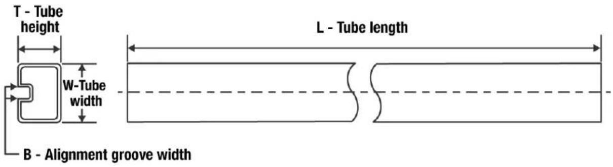
TUBE
text_image
T - Tube height L - Tube length W-Tube width B - Alignment groove width*All dimensions are nominal
| Device | Package Name | Package Type | Pins | SPQ | L (mm) | W (mm) | T (μm) | B (mm) |
| 5962-9223802M2A FK | LCCC 20 1 506.98 1 | 2.06 2030 NA | ||||||
| CY54FCT573ATLMB FK | LCCC 20 1 506.98 | 12.06 2030 NA | ||||||
| CY74FCT573ATPC | N | PDIP | 20 | 20 | 506 | 13.97 | 11230 | 4.32 |
| CY74FCT573ATSOC | DW | SOIC | 20 | 25 | 507 | 12.83 | 5080 | 6.6 |
| CY74FCT573CTSOC | DW | SOIC | 20 | 25 | 507 | 12.83 | 5080 | 6.6 |
| CY74FCT573CTSOCG4 | DW | SOIC | 20 | 25 | 507 | 12.83 | 5080 | 6.6 |
| CY74FCT573TSOC | DW | SOIC | 20 | 25 | 507 | 12.83 | 5080 | 6.6 |
IMPORTANT NOTICE AND DISCLAIMER
TI PROVIDES TECHNICAL AND RELIABILITY DATA (INCLUDING DATA SHEETS), DESIGN RESOURCES (INCLUDING REFERENCE DESIGNS), APPLICATION OR OTHER DESIGN ADVICE, WEB TOOLS, SAFETY INFORMATION, AND OTHER RESOURCES "AS IS" AND WITH ALL FAULTS, AND DISCLAIMS ALL WARRANTIES, EXPRESS AND IMPLIED, INCLUDING WITHOUT LIMITATION ANY IMPLIED WARRANTIES OF MERCHANTABILITY, FITNESS FOR A PARTICULAR PURPOSE OR NON-INFRINGEMENT OF THIRD PARTY INTELLECTUAL PROPERTY RIGHTS.
These resources are intended for skilled developers designing with TI products. You are solely responsible for (1) selecting the appropriate TI products for your application, (2) designing, validating and testing your application, and (3) ensuring your application meets applicable standards, and any other safety, security, regulatory or other requirements.
These resources are subject to change without notice. TI grants you permission to use these resources only for development of an application that uses the TI products described in the resource. Other reproduction and display of these resources is prohibited. No license is granted to any other TI intellectual property right or to any third party intellectual property right. TI disclaims responsibility for, and you will fully indemnify TI and its representatives against, any claims, damages, costs, losses, and liabilities arising out of your use of these resources.
TI's products are provided subject to TI's Terms of Sale or other applicable terms available either on ti.com or provided in conjunction with such TI products. TI's provision of these resources does not expand or otherwise alter TI's applicable warranties or warranty disclaimers for TI products.
TI objects to and rejects any additional or different terms you may have proposed.
Mailing Address: Texas Instruments, Post Office Box 655303, Dallas, Texas 75265
Copyright © 2022, Texas Instruments Incorporated