OPA209AID - Electronic component TEXAS INSTRUMENTS - Free user manual and instructions
Find the device manual for free OPA209AID TEXAS INSTRUMENTS in PDF.

User questions about OPA209AID TEXAS INSTRUMENTS
0 question about this device. Answer the ones you know or ask your own.
Ask a new question about this device
Download the instructions for your Electronic component in PDF format for free! Find your manual OPA209AID - TEXAS INSTRUMENTS and take your electronic device back in hand. On this page are published all the documents necessary for the use of your device. OPA209AID by TEXAS INSTRUMENTS.
USER MANUAL OPA209AID TEXAS INSTRUMENTS
OPAx2092.2-nV/√Hz, Low-Power, 36-VOperationalAmplifier
1Features
•LowVoltageNoise:2.2nV/√Hzat1kHz
•0.1-Hzto10-HzNoise:130nV PP
- LowQuiescentCurrent:2.5mA/Ch(Maximum)
- LowOffsetVoltage:150μV(Maximum)
•GainBandwidthProduct:18MHz
•SlewRate:6.4V/μs
•WideSupplyRange: ±2.25Vto±18V,4.5Vto36V
•Rail-to-RailOutput
•Short-CircuitCurrent:±65mA
•Availablein5-PinSOT-23,8-PinMSOP, 8-PinSOIC,and14-PinTSSOPPackages
2Applications
- PLLLoopFilters
- Low-Noise, Low-PowerSignalProcessing
•Low-NoiseInstrumentationAmplifiers
•High-PerformanceADCDrivers
•High-PerformanceDACOutputAmplifiers
•ActiveFilters
•UltrasoundAmplifiers
•ProfessionalAudioPreamplifiers - Low-NoiseFrequencySynthesizers
• InfraredDetectorAmplifiers
•HydrophoneAmplifiers
3Description
The OPA209 series of precision operational amplifiers achieve every low voltage and are noised density (2.2 nV/√Hz) with supply current only 2.5 mA (maximum). This series also offers rail-to-rail output swing, which helps to maximize dynamic range.
Inprecisiondataacquisitionapplications,the OPA209providesfastsettlingtimeto16-bitaccuracy, evenfor10-Voutputswings. Thisexcellentac performance, combined with only 150 μV (maximum) ofoffsetandlowdriftovertemperature,makes the OPA209verysuitableforfast,high-precision applications.
The OPA209 is specified over a wide dual power-supply range of ±2.25V to ±18V , or single-supply operation from 4.5V to 36V.
The OPA209 is available in the 5-pin SOT-23, 8-pin VSSOP, and the standard8-pinSOIC packages. The dualOPA2209 comes in both 8-pin VSSOP and 8-pin SOIC packages. The quad OPA4209 is available in the 14-pin TSSOP package.
TheOPA209seriesisspecifiedfrom-40°Cto125°C.
DeviceInformation (1)
(1) For all available packages, see the orderable addendum at the endofthedatasheet.
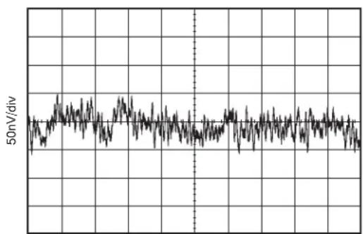
0.1-Hzto10-HzNoise
line
| Time | 50nV/div | |------|----------| | 0 | ~0 | | 1 | ~0 | | 2 | ~0 | | 3 | ~0 | | 4 | ~0 | | 5 | ~0 | | 6 | ~0 | | 7 | ~0 | | 8 | ~0 | | 9 | ~0 | | 10 | ~0 | | 11 | ~0 | | 12 | ~0 | | 13 | ~0 | | 14 | ~0 | | 15 | ~0 | | 16 | ~0 | | 17 | ~0 | | 18 | ~0 | | 19 | ~0 | | 20 | ~0 | | 21 | ~0 | | 22 | ~0 | | 23 | ~0 | | 24 | ~0 | | 25 | ~0 | | 26 | ~0 | | 27 | ~0 | | 28 | ~0 | | 29 | ~0 | | 30 | ~0 | | 31 | ~0 | | 32 | ~0 | | 33 | ~0 | | 34 | ~0 | | 35 | ~0 | | 36 | ~0 | | 37 | ~0 | | 38 | ~0 | | 39 | ~0 | | 40 | ~0 | | 41 | ~0 | | 42 | ~0 | | 43 | ~0 | | 44 | ~0 | | 45 | ~0 | | 46 | ~0 | | 47 | ~0 | | 48 | ~0 | | 49 | ~0 | | 50 | ~0 |Time (1s/div)
TableofContents
1 Features.... 1
2 Applications 1
3 Description 1
4 Revision History...... 2
5PinConfigurationandFunctions....3
6 Specifications.... 5
6.1 AbsoluteMaximumRatings....5
6.2ESDRatings....5
6.3RecommendedOperatingConditions....5
6.4ThermalInformation:OPA209....5
6.5ThermalInformation:OPA2209....6
6.6ThermalInformation:OPA4209....6
6.7 Electrical Characteristics....6
6.8TypicalCharacteristics....8
7DetailedDescription....13
7.1Overview....13
7.2FunctionalBlockDiagram....13
7.3FeatureDescription....13
7.4DeviceFunctionalModes....17
8ApplicationandImplementation....18
8.1 Application Information....18
8.2TypicalApplication....18
9PowerSupplyRecommendations....19
10 Layout.... 19
10.1 Layout Guidelines 19
10.2LayoutExample....20
11DeviceandDocumentationSupport....21
11.1DeviceSupport....21
11.2DocumentationSupport....22
11.3RelatedLinks....22
11.4ReceivingNotificationofDocumentationUpdates22
11.5CommunityResources....22
11.6Trademarks....22
11.7ElectrostaticDischargeCaution....22
11.8Glossary....23
12Mechanical, Packaging, and Orderable Information 23
4 RevisionHistory
NOTE: Pagenumbersforpreviousrevisionsmaydifferfrompagenumbersinthecurrentversion.
ChangesfromRevisionC(October2013)toRevisionD
Page
- Added ESD Ratings table, Feature Description section, Device Functional Modes, Application and Implementation section, Power Supply Recommendations section, Layout section, Device and Documentation Support section, and Mechanical, Packaging, and Orderable Information section.... 1
- Deleted Ordering Information table; see POA at the end of the data sheet.... 1
- Moved specified voltage, specified temperature, and operating temperature from Electrical Characteristics to Recommended Operating Conditions .... 5
- Updated values in the Thermal Information tables to align with JEDEC standards.... 5
ChangesfromRevisionB(August2010)toRevisionC
Page
- Deleted device graphic 1
- Changed y-axis units label in Figure 2....8
5PinConfigurationandFunctions
OPA209:DBVPackage
5-PinSOT-23
TopView
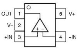
text_image
OUT 1 V- 2 +IN 3 5 V+ 4 -INOPA209:DorDGKPackages
8-PinSOICorVSSOP
TopView
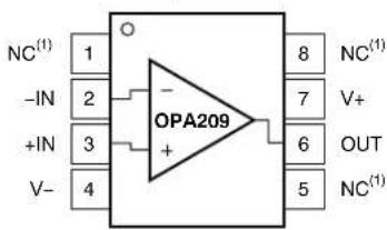
text_image
NC(1) 1 -IN 2 +IN 3 V- 4 OPA209 - + 8 NC(1) 7 V+ 6 OUT 5 NC(1)(1)NC=nointernalconnection
PinFunctions:OPA209
| PIN | I/ODESCRIPTION | ||
| NAMESOT-23SOIC,VSSOP | |||
| -IN42 | I | Invertinginput | |
| +IN33 | I | Noninvertinginput | |
| NC | — | 1, 5, 8 | — No internal connection |
| OUT | 16 | O Output | |
| V- | 24 | — Negative(lowest)powersupply | |
| V+ | 5 | 7 | — Positive (highest) power supply |
OPA2209:DorDGKPackages
8-PinSOICorVSSOP
TopView

text_image
OUT A 1 -IN A 2 +IN A 3 V- 4 A + B + 8 V+ 7 OUT B 6 -IN B 5 +IN BPinFunctions:OPA2209
| PIN | I/O | DESCRIPTION | |
| NAME | NO. | ||
| -INA | 2 | I | Invertinginput,channelA |
| +INA | 3 | I | Noninvertinginput,channelA |
| -INB | 6 | I | Invertinginput,channelB |
| +INB | 5 | I | Noninvertinginput,channelB |
| OUTA | 1 | O | Output,channelA |
| OUTB | 7 | O | Output,channelB |
| V- | 4 | — | Negative(lowest)powersupply |
| V+ | 8 | — | Positive(highest)powersupply |
OPA4209:PWPackage
14-PinTSSOP
TopView

text_image
OUT A 1 -IN A 2 +IN A 3 V+ 4 +IN B 5 -IN B 6 OUT B 7 -A +B -D+ -C+ 14 OUT D 13 -IN D 12 +IN D 11 V- 10 +IN C 9 -IN C 8 OUT CPinFunctions:OPA4209
| PIN | I/ODESCRIPTION | ||
| NAMENO. | |||
| -INA2IInvertinginput,channelA | |||
| +INA3INoninvertinginput,channelA | |||
| -INB6IInvertinginput,channelB | |||
| +INB5INoninvertinginput,channelB | |||
| -INC9IInvertinginput,channelC | |||
| +INC10INoninvertinginput,channelC | |||
| -IND13IInvertinginput,channelD | |||
| +IND12INoninvertinginput,channelD | |||
| OUTA | 1O Output,channelA | ||
| OUTB | 7O Output,channelB | ||
| OUTC | 8O Output,channelC | ||
| OUTD | 14 O Output,channelD | ||
| V- | 11 — Negative(lowest)powersupply | ||
| V+ | 4 — Positive(highest)powersupply | ||
6Specifications
6.1 AbsoluteMaximumRatings
overoperatingfree-airtemperaturerange(unlessotherwisenoted) (1)
| MINMAXUNIT | ||||
| Voltage | Supplyvoltage, V_S = (V+) - (V-)40V | |||
| Signalinputpins^(2) | (V-) - 0.5(V+) + 0.5 | V | ||
| Current | Signalinputpins^(2) | -10 | 10 | mA |
| Outputshortcircuit^(3) | Continuous | |||
| Temperature | Operating, T_A | -55 | 150°C | |
| Junction, T_J | 200°C | |||
| Storage, T_stg | -65 | 150°C | ||
(1) Stresses beyond those listed under Absolute Maximum Ratings may cause permanent damage to the device. These are stress ratings only, which do not imply functional operation of the device at these or any other conditions beyond those indicated under Recommended Operating Conditions. Exposure to absolute-maximum-rated conditions for extended periods may affect device reliability.
(2) For input voltages beyond the power-supply rails, voltage or current must be limited.
(3) Short-circuitoground, oneamplifierperpackage.
6.2ESDRatings
| VALUE | UNIT | ||
| V_(ESD) Electrostaticdischarge | Human-bodymodel(HBM),perANSI/ESDA/JEDECJS-001 (1) | ±3000 | V |
| Charged-devicemodel(CDM),perJEDECspecificationJESD22-C101 (2) | ±1000 | ||
(1)JEDECdocumentJEP155statesthat500-VHBMallowssafemanufacturingwithastandardESDcontrolprocess.
(2)JEDECdocumentJEP157statesthat250-VCDMallowssafemanufacturingwithastandardESDcontrolprocess.
6.3 Recommended Operating Conditions
overoperatingfree-airtemperaturerange(unlessotherwisenoted)
| MIN | MAX | UNIT | ||
| V_S | Specified voltage | ±2.25 | ±18 | V |
| Specified temperature | -40 | 125 | °C | |
| T_A | Operating temperature | -55 | 150 | °C |
6.4ThermalInformation:OPA209
| THERMALMETRIC (1) | OPA209 | UNIT | |||
| DBV(SOT-23) | D(SOIC) | DGK(VSSOP) | |||
| 5PINS | 8PINS8PINS | ||||
| R_ JA | Junction-to-ambient thermal resistance | 204.9 | 135.5 | 142.6 | °C/W |
| R_ JC(top) | Junction-to-case (top) thermal resistance | 200 | 73.7 | 46.9 | °C/W |
| R_ JB | Junction-to-board thermal resistance | 113.1 | 61.9 | 63.5 | °C/W |
| _JT | Junction-to-top characterization parameter | 38.2 | 19.7 | 5.3 | °C/W |
| _JB | Junction-to-board characterization parameter | 104.9 | 54.8 | 62.8 | °C/W |
(1) For more information about traditional and new thermal metrics, see the Semiconductor and IC Package Thermal Metrics application report.
6.5ThermalInformation:OPA2209
| THERMALMETRIC (1) | OPA2209 | UNITD(S | ||
| 8PINS8PINS | ||||
| R_ JA | Junction-to-ambientthermalresistance134.3132.7°C/W | |||
| R_ JC(top) | Junction-to-case(top)thermalresistance72.1 | 38.5 | °C/W | |
| R_ JB | Junction-to-board thermal resistance | 60.7 | 52.1 | °C/W |
| _JT | Junction-to-top characterization parameter | 18.2 | 2.4 | °C/W |
| _JB | Junction-to-board characterization parameter | 53.8 | 52.8 | °C/W |
OIC)DGK(VSS
(1) For more information about traditional and new thermal metrics, see the Semiconductor and IC Package Thermal Metrics application report.
6.6ThermalInformation:OPA4209
| THERMALMETRIC (1) | OPA4209 | UNIT | |
| PW(TSSOP) | |||
| 14PINS | |||
| R_ JA | Junction-to-ambientthermalresistance | 112.9 | °C/W |
| R_ JC(top) | Junction-to-case(top)thermalresistance | 26.1 | °C/W |
| R_ JB | Junction-to-boardthermalresistance | 61 | °C/W |
| _JT | Junction-to-topcharacterizationparameter | 0.7 | °C/W |
| _JB | Junction-to-boardcharacterizationparameter | 59.2 | °C/W |
(1) For more information about traditional and new thermal metrics, see the Semiconductor and IC Package Thermal Metrics application report.
6.7 Electrical Characteristics
at V_S = ± 2.25 V to ± 18 V, T_A = 25^ , R_L = 10 kΩ connected to midsupply, and V_CM = V_OUT = midsupply (unless otherwise noted)
| PARAMETER | TEST CONDITIONS | MIN | TYP | MAX | UNIT | ||
| OFFSETVOLTAGE | |||||||
| V_OS | Inputoffsetvoltage | V_S =±15V, V_CM =0V | ±35 ±150 | μV | |||
| dV_OS/dT | Inputoffsetvoltagedrift | T_A =-40°Cto125°C | 1 3 | μV/°C | |||
| PSRR | vspowersupply | V_S =±2.25Vto±18V | T_A =25°C | 0.05 0.5 | μV/V | ||
| T_A =-40°Cto125°C | 1 | ||||||
| Channel separation | DC (dual and quad versions) | 1 | μV/V | ||||
| INPUTBIASCURRENT | |||||||
| I_B | Inputbiascurrent | V_CM =0V | T_A =25°C | ±1 ±4.5 | nA | ||
| T_A =-40°Cto85°C | ±8 | ||||||
| T_A =-40°Cto125°C | ±15 | ||||||
| I_OS | Inputoffsetcurrent | V_CM =0V | T_A =25°C | ±0.7 ±4.5 | nA | ||
| T_A =-40°Cto85°C | ±8 | ||||||
| T_A =-40°Cto125°C | ±15 | ||||||
| NOISE | |||||||
| e_n | Input voltage noise | f = 0.1 Hz to 10 Hz | 0.13 | μVpp | |||
| Noisedensity | f=10Hz | 3.3 | nV/√Hz | ||||
| f=100Hz | 2.25 | ||||||
| f=1kHz | 2.2 | ||||||
| I_n | Input current noise density | f = 1 kHz | 500 | fA/√Hz | |||
| INPUTVOLTAGERANGE | |||||||
| V_CM | Common-modevoltage range | (V-)+1.5 (V+)-1.5 | V | ||||
| CMRR | Common-moderejection ratio | (V-)+1.5V120 130dB | 120 130 | dB | |||
ElectricalCharacteristics(continued)
at V_S=±2.25Vto±18V,T A=25^,RL=10k connectedtomidsupply,and V_CM=V_OUT=midsupply(unlessotherwise) noted)
| PARAMETERTESTCONDITION | ONSMINTYPMAXUNIT | ||||
| INPUTIMPEDANCE | |||||
| Differential200||4 | kΩ ||pF | ||||
| Common-mode | 10^9 2 | Ω ||pF | |||
| OPEN-LOOPGAIN | |||||
| AOL | Open-loopvoltagegain | (V-)+0.2V<T_A=25°C126 132dB | 126 132 | dB | |
| R_L=10kΩ | T_A=-40°Cto125°C | 120 | |||
| (V-)+0.6V<T_A=25°C114 120dB | T_A=25°C | 114 120 | |||
| R_L=600Ω^(1) | T_A=-40°Cto125°C | 110 | |||
| FREQUENCYRESPONSE | |||||
| GBW | Gainbandwidthproduct | 18 | MHz | ||
| SR | Slewrate | 6.4 | V/μs | ||
| Φm | Phasemargin | R_L=10kΩ,C_L=25pF | 80 | ° | |
| t_S | Settlingtime | 0.1%,G=-1,10-Vstep, C_L=100pF | 2.1 | μs | |
| 0.0015%(16-bit),G=-1,10-Vstep, C_L=100pF | 2.6 | ||||
| Overloadrecoverytime | G=-1 | <1 | μs | ||
| THD+N | Totalharmonicdistortion+noise | G=+1,f=1kHz,V_O=20V PP,600Ω | 0.000025% | ||
| OUTPUT | |||||
| Voltageoutputswing | R_L=10kΩ,A_OL>130dB | (V-)+0.2 (V+)-0.2 | V | ||
| R_L=600Ω,A_OL>114dB | (V-)+0.6 (V+)-0.6 | ||||
| R_L=10kΩ,A_OL>120dB,T_A=-40°Cto125°C | (V-)+0.2 (V+)-0.2 | ||||
| I_SC | Short-circuitcurrent | V_S=±18V | ±65 | mA | |
| C_LOAD | Capacitiveloaddrive(stableoperation) | SeeTypicalCharacteristics | |||
| Z_O | Open-loopoutputimpedance | SeeTypicalCharacteristics | |||
| POWERSUPPLY | |||||
| I_Q | Quiescentcurrent(peramplifier) | I_O=0A | T_A=25°C | 2.2 2.5 | mA |
| T_A=-40°Cto125°C | 3.25 | ||||
(1) See Absolute Maximum Ratings for additional information.
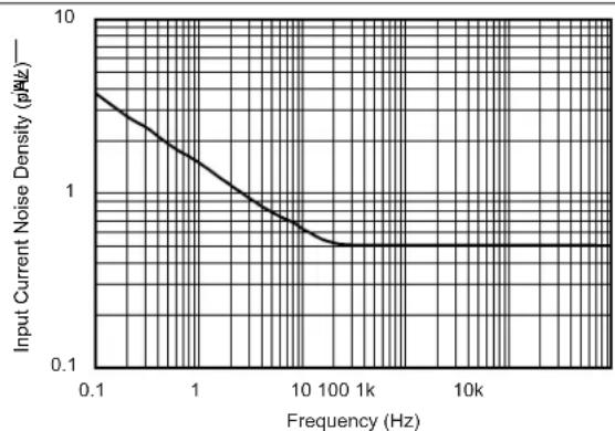
6.8 Typical Characteristics
at T_A = 25^ , V_S = ± 18 V, R_L = 10 kΩ connected to midsupply, and V_CM = V_OUT = midsupply (unless otherwise noted)

line
| Frequency (Hz) | Input Voltage Noise Density (nV/√Hz) | | -------------- | ------------------------------------ | | 0.1 | ~25 | | 1 | ~10 | | 10 | ~5 | | 100 | ~2 | | 1k | ~2 | | 10k | ~2 | | 100k | ~2 |Figure 1. Input Voltage Noise Density vs Frequency
line
| Frequency (Hz) | Input Current Noise Density (p/kz) | | -------------- | ---------------------------------- | | 0.1 | ~5.0 | | 1 | ~2.0 | | 10 | ~0.5 | | 100 | ~0.3 | | 1k | ~0.3 | | 10k | ~0.3 |Figure 2. Input Current Noise Density vs Frequency

Figure 3. Total Harmonic Distortion + Noise Ratio vs Frequency
line
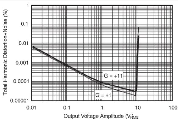
| Output Voltage Amplitude (V_RMS) | Total Harmonic Distortion+Noise (%) | | -------------------------------- | ------------------------------------ | | 0.01 | 0.01 | | 0.1 | 0.001 | | 1 | 0.0001 | | 10 | 0.00001 | | 100 | 0.000001 |Figure 4. Total Harmonic Distortion + Noise Ratio vs Amplitude

line
| Time (1s/div) | 50nV/div | | ------------- | -------- | | 0 | ~0 | | 1 | ~0 | | 2 | ~0 | | 3 | ~0 | | 4 | ~0 | | 5 | ~0 | | 6 | ~0 | | 7 | ~0 | | 8 | ~0 | | 9 | ~0 | | 10 | ~0 | | 11 | ~0 | | 12 | ~0 | | 13 | ~0 | | 14 | ~0 | | 15 | ~0 | | 16 | ~0 | | 17 | ~0 | | 18 | ~0 | | 19 | ~0 | | 20 | ~0 | | 21 | ~0 | | 22 | ~0 | | 23 | ~0 | | 24 | ~0 | | 25 | ~0 | | 26 | ~0 | | 27 | ~0 | | 28 | ~0 | | 29 | ~0 | | 30 | ~0 | | 31 | ~0 | | 32 | ~0 | | 33 | ~0 | | 34 | ~0 | | 35 | ~0 | | 36 | ~0 | | 37 | ~0 | | 38 | ~0 | | 39 | ~0 | | 40 | ~0 | | 41 | ~0 | | 42 | ~0 | | 43 | ~0 | | 44 | ~0 | | 45 | ~0 | | 46 | ~0 | | 47 | ~0 | | 48 | ~0 | | 49 | ~0 | | 50 | ~0 |Figure 5. 0.1-Hz to 10-Hz Noise
line
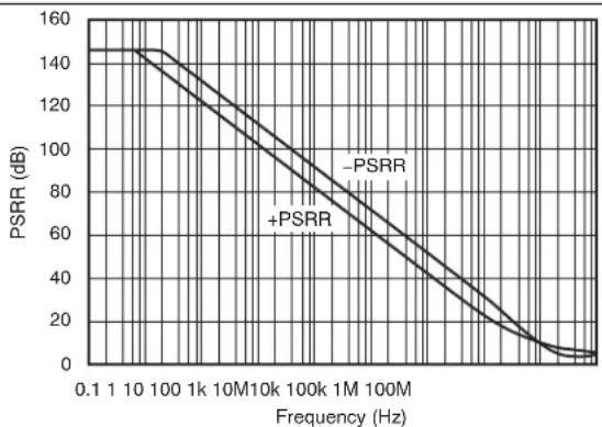
| Frequency (Hz) | +PSRR (dB) | -PSRR (dB) | | -------------- | ---------- | ---------- | | 0.1 | 145 | 145 | | 1 | 145 | 145 | | 10 | 145 | 145 | | 100 | 145 | 145 | | 1k | 145 | 145 | | 10M | 120 | 120 | | 10k | 100 | 100 | | 100k | 80 | 80 | | 1M | 60 | 60 | | 100M | 40 | 40 | | >100M | 20 | 20 | | >100M | 5 | 5 |Figure 6. Power-Supply Rejection Ratio vs Frequency (Referred to Input)
Typical Characteristics (continued)
at T_A = 25^ C , V_S = ± 18 V, R_L = 10 kΩ connected to midsupply, and V_CM = V_OUT = midsupply (unless otherwise noted)
line
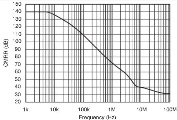
| Frequency (Hz) | CMRR (dB) | | -------------- | --------- | | 1k | 140 | | 10k | 135 | | 100k | 110 | | 1M | 70 | | 10M | 40 | | 100M | 30 |Figure 7. Common-Mode Rejection Ratio vs Frequency

line
| Frequency (Hz) | Open-Loop Output Impedance (Z₀) | | -------------- | ------------------------------- | | 0.1 | 100000 | | 1 | 10000 | | 10 | 1000 | | 100 | 100 | | 1k | 1 | | 10k | 1 | | 100k | 1 | | 1M | 10 | | 10M | 10 | | 100M | 10 |Figure 8. Open-Loop Output Impedance vs Frequency
line
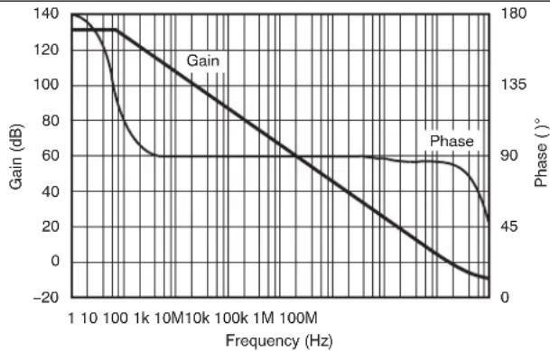
| Frequency (Hz) | Gain (dB) | Phase (°) | | -------------- | --------- | --------- | | 1 | 135 | 180 | | 10 | 130 | 175 | | 100 | 120 | 160 | | 1k | 100 | 135 | | 10M | 80 | 120 | | 10k | 60 | 105 | | 100k | 40 | 90 | | 1M | 20 | 85 | | 100M | 0 | 80 | | >100M | -20 | 45 |Figure 9. Open-Loop Gain and Phase vs Frequency
line
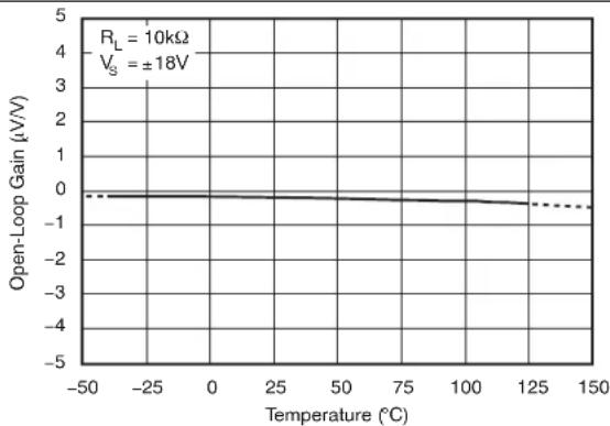
| Temperature (°C) | Open-Loop Gain (μV/V) | | ---------------- | --------------------- | | -50 | 0 | | 0 | 0 | | 25 | 0 | | 50 | 0 | | 75 | 0 | | 100 | 0 | | 125 | -1 | | 150 | -1 |Figure 10. Open-Loop Gain vs Temperature
histogram
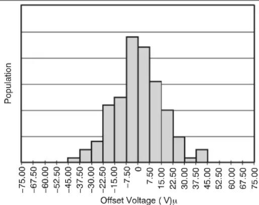
| Offset Voltage (V)μ | Population | |---|---| | -75.00 to -67.50 | 0 | | -67.50 to -60.00 | 0 | | -60.00 to -52.50 | 0 | | -52.50 to -45.00 | 1 | | -45.00 to -37.50 | 2 | | -37.50 to -30.00 | 3 | | -30.00 to -22.50 | 5 | | -22.50 to -15.00 | 8 | | -15.00 to -7.50 | 11 | | -7.50 to 0 | 16 | | 0 to 7.50 | 14 | | 7.50 to 15.00 | 11 | | 15.00 to 22.50 | 8 | | 22.50 to 30.00 | 4 | | 30.00 to 37.50 | 1 | | 37.50 to 45.00 | 3 | | 45.00 to 52.50 | 1 | | 60.00 to 67.50 | 0 | | 75.00 to 79.50 | 0 |Figure 11. Offset Voltage Production Distribution
histogram
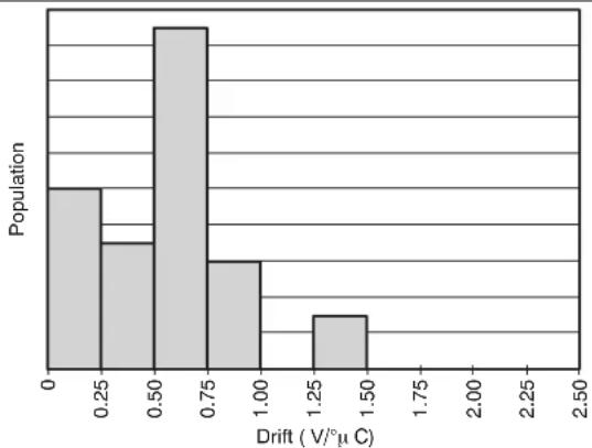
| Drift (V/°C) | Population | | :--- | :--- | | 0.25 | 100 | | 0.50 | 80 | | 0.75 | 160 | | 1.00 | 90 | | 1.25 | 30 | | 1.50 | 0 | | 1.75 | 0 | | 2.00 | 0 | | 2.25 | 0 | | 2.50 | 0 |Figure 12. Offset Voltage Drift Production Distribution
Typical Characteristics (continued)
at T_A = 25^ C , V_S = ± 18 V, R_L = 10 kΩ connected to midsupply, and V_CM = V_OUT = midsupply (unless otherwise noted)
line
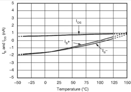
| Temperature (°C) | I_B (nA) | I_OS (nA) | | ---------------- | -------- | --------- | | -50 | -2.0 | 0.5 | | 0 | -1.5 | 0.5 | | 50 | -1.0 | 0.5 | | 100 | -0.5 | 0.5 | | 150 | 0.0 | 0.5 |Figure 13. Input Bias and Input Offset Currents vs Temperature
line
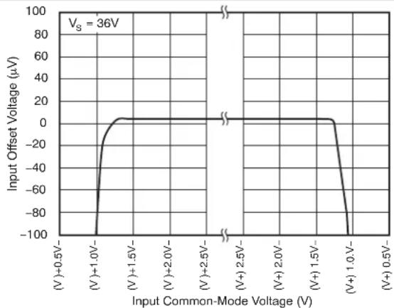
| Input Common-Mode Voltage (V) | Input Offset Voltage (µV) | | ----------------------------- | ------------------------- | | -0.5V | -100 | | -1.0V | -20 | | -1.5V | 0 | | -2.0V | 0 | | -2.5V | 0 | | 2.5V | 0 | | 2.0V | 0 | | 1.5V | 0 | | 1.0V | -20 | | 0.5V | -100 |Figure 14. Input Offset Voltage vs Common-Mode Voltage

line
| Time (s) | V_G Shift (μV) | | -------- | -------------- | | 0 | 4 | | 20 | 9 | | 40 | 10 | | 60 | 10.5 | | 80 | 10.7 | | 100 | 10.8 | | 120 | 10.9 |Figure 15. Input Offset Voltage vs Time
line
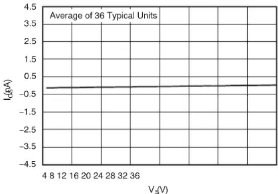
| Vs(V) | I_G(A) | |-------|--------| | 4 | -0.5 | | 8 | -0.5 | | 12 | -0.5 | | 16 | -0.5 | | 20 | -0.5 | | 24 | -0.5 | | 28 | -0.5 | | 32 | -0.5 | | 36 | -0.5 |Figure 16. Input Offset Current vs Supply Voltage

line
| Common-Mode Voltage (V) | I_B (μA) | I_G (μA) | | ----------------------- | -------- | -------- | | V+0.5V | -4 | -4 | | V+1.0V | -2 | -2 | | V+1.5V | 0 | 0 | | V+2.0V | 0 | 0 | | V+2.5V | 0 | 0 | | V+3.0V | 0 | 0 | | V+3.0V | 1 | 1 | | V+2.5V | 1 | 1 | | V+2.0V | 1 | 1 | | V+1.5V | 1 | 1 | | V+1.0V | 2 | 2 | | V+0.5V | 3 | 3 |Figure 17. Input Bias and Input Offset Currents vs Common-Mode Voltage
line
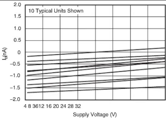
| Supply Voltage (V) | I_H (nA) | | ------------------ | -------- | | 4 | -1.5 | | 8 | -1.2 | | 12 | -0.9 | | 16 | -0.6 | | 20 | -0.3 | | 24 | 0.0 | | 28 | 0.3 | | 32 | 0.6 |Figure 18. Input Bias Current vs Supply Voltage
Typical Characteristics (continued)
at T_A = 25^ C , V_S = ± 18 V, R_L = 10 kΩ connected to midsupply, and V_CM = V_OUT = midsupply (unless otherwise noted)
line
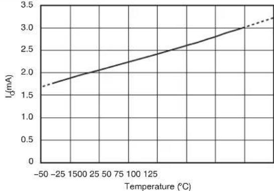
| Temperature (°C) | I_d (mA) | | ---------------- | -------- | | -50 | 1.7 | | 1500 | 2.0 | | 25 | 2.2 | | 50 | 2.4 | | 75 | 2.6 | | 100 | 2.8 | | 125 | 3.0 | | 150 | 3.2 | | 175 | 3.4 |Figure 19. Quiescent Current vs Temperature
line
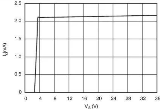
| Vs (V) | Id (mA) | | ------ | ------- | | 0 | 0 | | 4 | 2.1 | | 8 | 2.1 | | 12 | 2.1 | | 16 | 2.1 | | 20 | 2.1 | | 24 | 2.1 | | 28 | 2.1 | | 32 | 2.1 | | 36 | 2.1 |Figure 20. Quiescent Current vs Supply Voltage
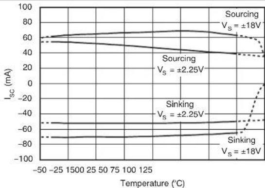
Figure 21. Short-Circuit Current vs Temperature
line
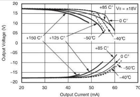
| Output Current (mA) | +85 C° | -50 C° | -40 C° | 0 C° | -50 C° | -40 C° | | ------------------- | ------ | ------ | ------ | ---- | ------ | ------ | | 20 | 17 | 17 | 17 | 17 | 17 | 17 | | 30 | 16 | 16 | 16 | 16 | 16 | 16 | | 40 | 14 | 14 | 14 | 14 | 14 | 14 | | 50 | 10 | 10 | 10 | 10 | 10 | 10 | | 60 | 5 | 5 | 5 | 5 | 5 | 5 | | 70 | 0 | 0 | 0 | 0 | 0 | 0 |Figure 22. Output Voltage vs Output Current

text_image
G = +1 R_L = 604Ω C_L = 100pF 20mV/div Device +18V -18V R_L C_L Time (0.1 s/div)µFigure 23. Small-Signal Step Response
text_image
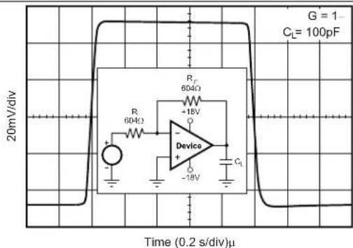
G = 1 CL= 100pF 20mV/div Rf 804Ω +18V R 604Ω Device + - -18V CL Time (0.2 s/div)μFigure 24. Small-Signal Step Response
Typical Characteristics (continued)
at T_A = 25^ C , V_S = ± 18 V, R_L = 10 kΩ connected to midsupply, and V_CM = V_OUT = midsupply (unless otherwise noted)

text_image
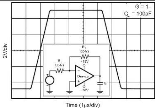
2V/div G = +1 R_L = 604Ω C_L = 100pF Time (1μs/div)Figure 25. Large-Signal Step Response
line
| Parameter | Value | | --------- | --------- | | G | 1- | | C_L | 100pF | | RF | 604Ω | | R_F | +18V | | R_1 | 604Ω | | R_2 | -18V | | Q | -18V |Figure 26. Large-Signal Step Response
line
| Time (ms) | 5V/div | | --------- | ------ | | 0.00 | 0 | | 0.25 | Peak | | 0.50 | 0 | | 1.00 | -18 | | 1.50 | 0 | | 2.00 | 18 | | 2.50 | 0 | | 3.00 | -18 | | 3.50 | 0 | | 4.00 | 18 | | 4.50 | 0 | | 5.00 | -18 | | 5.50 | 0 | | 6.00 | 18 | | 6.50 | 0 | | 7.00 | -18 | | 7.50 | 0 | | 8.00 | 18 | | 8.50 | 0 | | 9.00 | -18 | | 9.50 | 0 | | 10.00 | 18 | | 10.50 | 0 | | 11.00 | -18 | | 11.50 | 0 | | 12.00 | 18 | | 12.50 | 0 | | 13.00 | -18 | | 13.50 | 0 | | 14.00 | 18 | | 14.50 | 0 | | 15.00 | -18 | | 15.50 | 0 | | 16.00 | 18 | | 16.50 | 0 | | 17.00 | -18 | | 17.50 | 0 | | 18.00 | 18 | | 18.50 | 0 | | 19.00 | -18 | | 19.50 | 0 | | 20.00 | 18 | | 20.50 | 0 | | 21.00 | -18 | | 21.50 | 0 | | 22.00 | 18 | | 22.50 | 0 | | 23.00 | -18 | | 23.50 | 0 | | 24.00 | 18 | | 24.50 | 0 | | 25.00 | -18 |Figure27. NoPhase Reversal
line
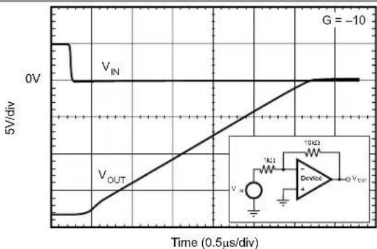
| Time (0.5μs/div) | V_IN (5V/div) | V_OUT (5V/div) | | ---------------- | ------------- | -------------- | | 0 | 0 | 0 | | 0.5 | 0 | ~0.2 | | 1.0 | 0 | ~0.4 | | 1.5 | 0 | ~0.6 | | 2.0 | 0 | ~0.8 | | 2.5 | 0 | ~1.0 | | 3.0 | 0 | ~1.2 | | 3.5 | 0 | ~1.4 | | 4.0 | 0 | ~1.6 | | 4.5 | 0 | ~1.8 | | 5.0 | 0 | ~2.0 | | 5.5 | 0 | ~2.2 | | 6.0 | 0 | ~2.4 | | 6.5 | 0 | ~2.6 | | 7.0 | 0 | ~2.8 | | 7.5 | 0 | ~3.0 | | 8.0 | 0 | ~3.2 | | 8.5 | 0 | ~3.4 | | 9.0 | 0 | ~3.6 | | 9.5 | 0 | ~3.8 | | 10.0 | 0 | ~4.0 | | 10.5 | 0 | ~4.2 | | 11.0 | 0 | ~4.4 | | 11.5 | 0 | ~4.6 | | 12.0 | 0 | ~4.8 | | 12.5 | 0 | ~5.0 | | 13.0 | 0 | ~5.2 | | 13.5 | 0 | ~5.4 | | 14.0 | 0 | ~5.6 | | 14.5 | 0 | ~5.8 | | 15.0 | 0 | ~6.0 | | 15.5 | 0 | ~6.2 | | 16.0 | 0 | ~6.4 | | 16.5 | 0 | ~6.6 | | 17.0 | 0 | ~6.8 | | 17.5 | 0 | ~7.0 | | 18.0 | 0 | ~7.2 | | 18.5 | 0 | ~7.4 | | 19.0 | 0 | ~7.6 | | 19.5 | 0 | ~7.8 | | 20.0 | 0 | ~8.0 | | 20.5 | 0 | ~8.2 | | 21.0 | 0 | ~8.4 | | 21.5 | 0 | ~8.6 | | 22.0 | 0 | ~8.8 | | 22.5 | 0 | ~9.0 | | 23.0 | 0 | ~9.2 | | 23.5 | 0 | ~9.4 | | 24.0 | 0 | ~9.6 | | 24.5 | 0 | ~9.8 | | 25.0 | 0 | ~10.0 | | 25.5 | 0 | ~10.2 | | 26.0 | 0 | ~10.4 | | 26.5 | 0 | ~10.6 | | 27.0 | 0 | ~10.8 | | 27.5 | 0 | ~11.0 | | 28.0 | 0 | ~11.2 | | 28.5 | 0 | ~11.4 | | 29.0 | 0 | ~11.6 | | 29.5 | 0 | ~11.8 | | 30.0 | 0 | ~12.0 | | 30.5 | 0 | ~12.2 | | 31.0 | 0 | ~12.4 | | 31.5 | 0 | ~12.6 | | 32.0 | 0 | ~12.8 | | 32.5 | 0 | ~13.0 | | 33.0 | 0 | ~13.2 | | 33.5 | 0 | ~13.4 | | 34.0 | 0 | ~13.6 | | 34.5 | 0 | ~13.8 | | 35.0 | 0 | ~14.0 | | 35.5 | 0 | ~14.2 | | 36.0 | 0 | ~14.4 | | 36.5 | 0 | ~14.6 | | 37.0 | 0 | ~14.8 | | 37.5 | 0 | ~15.0 | | 38.0 | 0 | ~15.2 | | 38.5 | 0 | ~15.4 | | 39.0 | 0 | ~15.6 | | 39.5 | 0 | ~15.8 | | 40.0 | 0 | ~16.0 | | 40.5 | 0 | ~16.2 | | 41.0 | 0 | ~16.4 | | 41.5 | 0 | ~16.6 | | 42.0 | 0 | ~16.8 | | 42.5 | 0 | ~17.0 | | 43.0 | 0 | ~17.2 | | 43.5 | 0 | ~17.4 | | 44.0 | 0 | ~17.6 | | 44.5 | 0 | ~17.8 | | 45.0 | 0 | ~18.0 | | 45.5 | 0 | ~18.2 | | 46.0 | 0 | ~18.4 | | 46.5 | 0 | ~18.6 | | 47.0 | 0 | ~18.8 | | 47.5 | 0 | ~19.0 | | 48.0 | 0 | ~19.2 | | 48.5 | 0 | ~19.4 | | 49.0 | 0 | ~19.6 | | 49.5 | 0 | ~19.8 | | 50.0 | 0 | ~20 | | G = -10 | - | - | The chart includes a secondary axis labels for 'V_IN' and 'V_OUT' in the top left panel, and a secondary axis labels for 'V_OUT' in the bottom left panel, with a secondary axis label 'Device' in the center of the right panel.Figure28. NegativeOverload Recovery
line
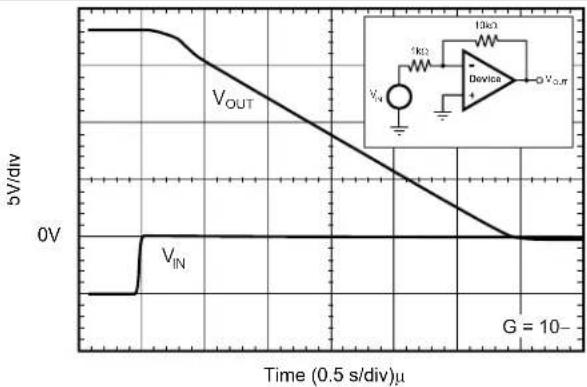
| Time (0.5 s/div)μ | VOUT (V/V/div) | VIN (V/V/div) | | ----------------- | -------------- | ------------- | | 0 | ~1V | 0V | | 0.5 | ~0.5V | ~0V | | 10 | ~0V | 0V |Figure29. PositiveOvervoltage Recovery

line
| Capacitive Load (pF) | Overshoot (%) G = +1 | Overshoot (%) G = 1- | | --------------------- | -------------------- | -------------------- | | 0 | 10 | 2 | | 200 | 15 | 5 | | 400 | 25 | 10 | | 600 | 35 | 18 | | 800 | 40 | 25 | | 1000 | 45 | 30 | | 1200 | 48 | 35 | | 1400 | 50 | 40 | | 1600 | 52 | 45 | | 1800 | 54 | 48 |Figure30. Small-SignalOvershoot vsCapacitive Load
7DetailedDescription
7.1Overview
The OPA209 series of precision operational amplifiers are unity-gainstable, and free from unexpected output and phasereversal. Applications with noisy or high-impedance powers supplies require decoupling capacitors placed close to the device pins. In most cases, 0.1- F capacitors are adequate. The Functional Block Diagram shows asimplified schematic of the OPA209. This dieuses a Si Gebipolar process and contains 180 transistors.
7.2FunctionalBlockDiagram

text_image
V+ Pre-Output Driver OUT IN- IN+ V- Copyright © 2016, Texas Instruments Incorporate7.3FeatureDescription
7.3.1 Operating Voltage
TheOPA209seriesofopampscanbeusedwithsingleordualsupplieswithinanoperatingrangeofV (±2.25V)upto36V(±18V).Supplyvoltageshigherthan40Vtotalcanpermanentlydamagethedevice(see AbsoluteMaximumRatings).
Inaddition, keyparameters are assured over the specified temperature range, T _A = -40^125^ . Parameters that vary significantly with operating voltage or temperature are shown in the Typical Characteristics.
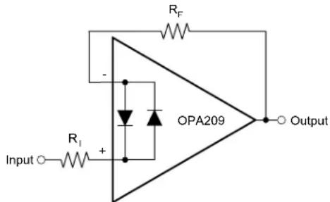
7.3.2 Input Protection
The input terminal so the OPA209 are protected from excessive differential voltage with back-to-back diodes, as shown in Figure 31. In most circuit applications, the input protection circuitry has no consequence. However, in low-gainor G=1 circuits, fast ramping inputs signals can forward-biasthesediodes because the output of the amplifier cannot respond rapidly enough to the input ramp. This effect is illustrated in Figure 25 and Figure 26 in Typical Characteristics. If the input signal is fast enough to create this forward-bias condition, the input signal current must be limited to 10 mA or less. If the input signal current is not inherently limited, an input series resistor can be used to limit the signal input current. This input series resistor degrades the low-noise performance of the OPA209. See Noise Performance for further information on noise performance.
FeatureDescription(continued)
Figure 31 shows an example configuration that implements a current-limiting feedback resistor.
Copyright © 2016, Texas Instruments Incorporated
Figure 31. Pulsed Operation
7.3.3 Noise Performance
Figure 32 shows the total circuit noise for varying source impedances with the op amp in a unity-gain configuration (no feedback resistor network, and therefore no additional noise contributions). Two different op amps are shown with the total circuit noise calculated. The OPA209 has very low voltage noise, making it ideal for low source impedances (less than 2 kΩ). As a comparable precision FET-input op amp (very low current noise), the OPA827 has somewhat higher voltage noise, but lower current noise. It provides excellent noise performance at moderate to high source impedance (10 kΩ and up). For source impedance lower than 300 Ω, the OPA211 may provide lower noise.
The equation in Figure 32 shows the calculation of the total circuit noise, with these parameters:
• e_n= voltage noise,
• i_n = current noise,
• R_S = source impedance,
• k = Boltzmann's constant = 1.38 × 10^-23 J/K, and
• T = temperature in Kelvins
For more details on calculating noise, see Basic Noise Calculations.

line
| Source Resistance, Rs(Ω) | Voltage Noise Spectral Density, E0 (OPA827) | Voltage Noise Spectral Density, E0 (OPA209) | | ------------------------ | ------------------------------------------ | ------------------------------------------ | | 100 | ~1 | ~1 | | 1k | ~10 | ~10 | | 100k | ~100 | ~100 | | 1M | ~1000 | ~1000 |Figure 32. Noise Performance of the OPA209 and OPA827 in Unity-Gain Buffer Configuration
FeatureDescription(continued)
7.3.4 BasicNoiseCalculations
Low-noise circuit design requires careful analysis of all noise sources. External noise sources can dominate in many cases; consider the effect of source resistance on overall op amp noise performance. Total noise of the circuitistheroot-sum-squarecombinationsofallnoisecomponents.
The resistive portion of the source impedance produces thermal noise proportional to the square root of the resistance. This function is illustrated in Figure 32. The source impedance is usually fixed; consequently, select the appropriate opamp and the feedback resistor to minimize the respective contribution to the total noise.
Figure 33 illustrates both noninverting (Figure 33a) and inverting (Figure 33b) op amp circuit configurations with gain. Incircuit configurations with gain, the feedback network resistors also contribute noise. The current noise of the opampreacts with the feedback resistor to create additional noise components.
The feedback resistor values can generally be chosen to make these noise sources negligible. Note that low-impedance feedback resistors load the output of the amplifier. The equations for total noise are shown for both configurations.
A) Noise in Noninverting Gain Configuration
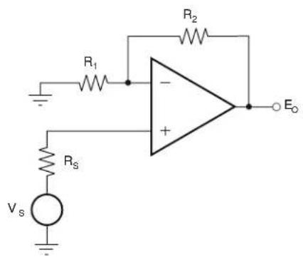
text_image
R₁ R₂ E₀ + - Rs VₛNoise at the output:
$$ E _ {0} ^ {2} = \left(1 + \frac {R _ {2}}{R _ {1}}\right) ^ {2} e _ {n} ^ {2 2 2 2 2 2} + e _ {2} + (i R _ {n}) + e _ {3} + (i R _ {n}) \left(1 + \frac {R _ {2}}{R _ {1}}\right) ^ {2} $$
$$ \text { Where } e _ {S} = \sqrt {4 k T R _ {S}} \times \left[ \begin{array}{c} R _ {2} \ R _ {1} \end{array} \right] \text { noise of } R \tag {s} $$
$$ e _ {1} = \sqrt [ 3 ]{4 k T R _ {1}} \times \left[ \begin{array}{l} R _ {2} \ R _ {1} \end{array} \right] \text { thermal noise of } R $$
$$ \mathrm{e} _ {2} = \sqrt {4 k T R _ {2}} = \text { thermal noise of } P _ {2} $$
B) Noise in Inverting Gain Configuration
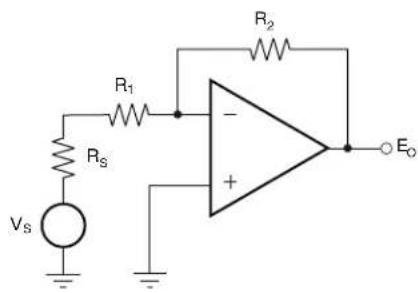
text_image
R2 Rs Vs - + EoNoise at the output:
$$ E _ {0} ^ {2} = \left[ 1 + \frac {R _ {2}}{R _ {1} + R _ {s}} \right] ^ {2} e _ {n 1} ^ {2 2 2 2 2} e _ {n 2 s} + e + (i R) + e $$
$$ \text { Where } e _ {s} = \sqrt {4 k T R _ {s}} \times \left[ \frac {R _ {2}}{R _ {1} + R _ {s}} \right] \text { noise of } R $$
$$ \mathrm{e} _ {1} = \sqrt [ 3 ]{4 \mathrm{kTR} _ {1}} \times \left[ \frac {\mathrm{R} _ {2}}{\mathrm{R} _ {1} + \mathrm{R} _ {\mathrm{s}}} \right] = \text { thermal noise of } \mathrm{R} _ {1} $$
$$ e _ {2} = \sqrt {4 k T R _ {2}} = \text { thermal noise of } R _ {2} $$
For the OPA209 series op amps at 1 kHz, e_n = 2.2 nV/√Hz and I_n = 530 fA/√Hz.
Figure33. NoiseCalculationinGainConfigurations
FeatureDescription(continued)
7.3.5 ElectricalOverstress
Designersoftenaskquestionsaboutthecapabilityofanoperationalamplifiertowithstandelectricaloverstress. Thesequestionstendtofocusonthedeviceinputs,butmayinvolvethesupplyvoltagepinsoreventheoutput pin.Eachofthesedifferentpinfunctionshaveelectricalstresslimitsdeterminedbythevoltagebreakdown characteristicsoftheparticularsemiconductorfabricationprocessandspecificcircuitsconnectedtothepin. Additionally,internalelectrostaticdischarge(ESD)protectionisbuiltintothesecircuitstoprotectthemfrom accidentalESDeventsbothbeforeandduringproductassembly.
ItishelpfultohaveagoodunderstandingofthisbasicESDcircuitryanditsrelevancetoanelectricaloverstress event. See Figure 34 for an illustration of the ESD circuits contained in the OPA209 series (indicated by the dashedlinearea).TheESDprotectioncircuitryinvolvesseveralcurrent-steeringdiodesconnectedfromtheinput andoutputpinsandroutedbacktotheinternalpower-supplylines,wheretheymeetatanabsorptiondevice internaltotheoperationalamplifier.Thisprotectioncircuitryisintendedtoremaininactivatedduringnormalcircuit operation.
AnESDeventproducesashortduration,high-voltagepulsethatistransformedintoashortduration,high-currentpulseasitdischargestroughasemiconductordevice.TheESDprotectioncircuitsaredesignedto provideacurrentpatharoundtheoperationalamplifiercoretopreventitfrombeingdamaged.Theenergy absorbedbytheprotectioncircuitryisthendissipatedasheat.
WhenanESDvoltagedevelopsacrosstwoormoreoftheamplifierdevicepins,currentflowsthroughoneor moreofthesteeringdiodes.Dependingonthepaththatthecurrenttakes,theabsorptiondevicemayactivate. Theabsorptiondevicehasatrigger,orthresholdvoltage,thatisabovethenormaloperatingvoltageofthe OPA209butbelowthevicebreakdownvoltagelevel.Oncethisthresholddisexceeded,theabsorptiondevice quicklyactivatesandclampsthevoltageacrossthesupplyrailstoasafelevel.
When the operational amplifier connects into a circuit such as the one Figure 34 shows, the ESD protection components are intended to remain inactive and not become involved in the application circuit operation. However, circumstances may arise where an applied voltage exceeds the operating voltage range of given pin. If this condition occurs, there is a risk that some of the internal ESD protection circuits may be biased on, and conduct current. Any such current flow occurs through steering diodepaths and rarely involve the absorption device.
Figure34 depicts a specific example where the input voltage, V in, exceeds the positive supply voltage (+V) by 500mVormore. Much of what happens in the circuit depends on the supply characteristics. If +V in cansink the current, one of the upper input steering diodes conducts and direct current to +V in Excessively high current levels can flow with increasingly higher V in. As a result, the datasheet specifications recommend that applications limit the input current to 10mA.
If the supply is not capable of sinking the current, V _IN may begin sourcing current to the operational amplifier, and then takeover asthesource of positives supply voltage. The danger in this case is that the voltage can rise to level that exceeds the operational amplifier absolute maximum ratings.
Another common question involves what happen to the amplifier if an input signal is applied to the input while the powers supplies + V S and/or - V S are at 0V.
Again, it depends on the supply characteristic while at 0 V, or at a level below the input signal amplitude. If the supplies appear as high impedance, then the operational amplifiers supply current may be supplied by the input source through the current steering diodes. This state is not an normal bias condition; the amplifier will not operate normally. If the supplies are low impedance, then the current through the steering diodes can become quite high. The current level depends on the ability of the input source to deliver current, and any resistance in the input path.
If there is an uncertainty about the ability of the supply to absorb this current, external Zener diodes may be added to the supply pins as shown in Figure 34. The Zener voltage must be selected such that the diode does not turn on during normal operation.
However, its Zenervoltagem must below enough so that the Zenerdiode conducts if the supply pin begins to be above safe operating supply voltage level.
FeatureDescription(continued)

text_image
TVS(2) RF +Vs +V - Ri Rs(3) -In +In Op Amp Core OPA209 Edge-Triggered ESD Absorption Circuit Out RL ID VIN(1) -V -VS -TVS(2)Copyright © 2016, Texas Instruments Incorporated
(1) V IN = +V S + 500mV
(2) TVS:+V S(max)>V TVSBR(Min)>+V S
(3)Suggestedvalueapproximately1kΩ
Figure34.EquivalentInternalESDCircuitryandItsRelationtoaTypicalCircuitApplication
7.4DeviceFunctionalModes
TheOPAx209isoperationalwhenthepower-supplyvoltageisgreaterthan4.5V(±2.25V). Themaximum power-supplyvoltagefortheOPAx209is36V(±18V).
8 Application and Implementation
NOTE
Information in the following applications sections is not part of the TI component specification, and TI does not warrant its accuracy or completeness. TI's customers are responsible for determining suitability of components for their purposes. Customers should validate and test their design implementation to confirm system functionality.
8.1 Application Information
The OPAx209 are unity-gain stable, precision operational amplifiers with very low noise. Applications with noisy or high-impedance power supplies require decoupling capacitors close to the device pins. In most cases, 0.1- F capacitors are adequate.
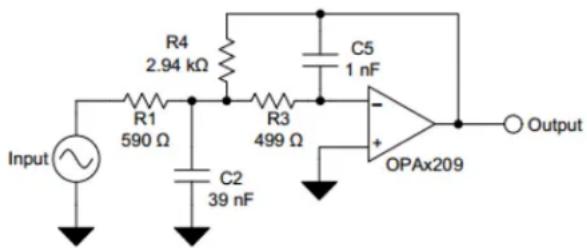
8.2 Typical Application
text_image
R4 2.94 kΩ C5 1 nF R1 590 Ω R3 499 Ω C2 39 nF OPAx209 Output Input ~Copyright © 2016, Texas Instruments Incorporated
Figure 35. Low-Pass Filter
8.2.1 Design Requirements
Low-pass filters are commonly employed in signal processing applications to reduce noise and prevent aliasing. The OPAx209 are ideally suited to construct high-speed, high-precision active filters. Figure 35 shows a second-order, low-pass filter commonly encountered in signal processing applications.
Use the following parameters for this design example:
• Gain = 5 V/V (inverting gain)
• Low-pass cutoff frequency = 25 kHz
• Second-order Chebyshev filter response with 3-dB gain peaking in the passband
8.2.2 Detailed Design Procedure
The infinite-gain multiple-feedback circuit for a low-pass network function is shown in Figure 35. Use Equation 1 to calculate the voltage transfer function.
$$ \frac {\text { Output }}{\text { Input }} (\mathrm{s}) = \frac {- 1 / R _ {1} R _ {2} C _ {5} C}{\mathrm{s} ^ {2} + (\mathrm{s} / G _ {2}) (1 / R _ {1} R _ {2} 1 / R _ {3} R _ {4} 2) 1 / R R C C} \tag {1} $$
This circuit produces a signal inversion. For this circuit, the gain at DC and the low-pass cutoff frequency are calculated by Equation 2:
$$ \text { Gain } = \frac {\mathrm{R} _ {4}}{\mathrm{R} _ {1}} $$
$$ f _ {c} \left(\frac {1}{2 \pi} R _ {5} R \sqrt {C C}\right) \tag {2} $$
TypicalApplication(continued)
8.2.3ApplicationCurve
line
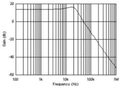
| Frequency (Hz) | Gain (dB) | | -------------- | --------- | | 100 | -50 | | 1k | -50 | | 10k | 15 | | 100k | -20 | | 1M | -50 |Figure36.OPAx209Second-Order,25-kHz,Chebyshev,Low-PassFilter
9PowerSupplyRecommendations
TheOPAx209isspecifiedforoperationfrom4.5Vto36V(±2.25Vto±18V);manyspecificationsapplyfrom -40°C to 125°C. Parametersthatcanexhibitsignificantvariancewithregardtooperatingvoltageortemperature arepresented in the TypicalCharacteristics.
10Layout
10.1 LayoutGuidelines
Forbestoperationalperformanceofthedevice,usegoodprintedcircuitboard(PCB)layoutpractices,including thefollowingguidelines:
- Noise can propagate into analog circuitry through the power pins of the circuit as a whole and op amp itself. Bypasscapacitorsareusedtoreducethecouplednoisebyprovidinglow-impedancepowersourceslocalto theanalogcircuitry.
- Connect low-ESR, 0.1-μF ceramic bypass capacitors between each supply pin and ground, placed as close to the device as possible. A single bypass capacitor from V+ to ground is applicable for single-supply applications.
- Separate grounding for analog and digital portions of circuitry is one of the simplest and most-effective methodsofnoisesuppression.OneormorelayeronmultilayerPCBsareusuallydevotedtogroundplanes.AgroundplanehelpsdistributeheatandreducesEMInoisepickup.Makesuretophysicallyseparatedigital andanaloggroundspayingattentiontotheflowofthegroundcurrent.
- To reduce parasitic coupling, run the input traces as far away from the supply or output traces as possible. If thesetracescannotbekeptseparate,crossingthesensitivetraceperpendicularismuchbetterasopposedto inparallelwiththenoisytrace.
- Placetheexternalcomponentsasclosetothedeviceaspossible.
- Keep the length of input traces as short as possible. Always remember that the input traces are the most sensitive part of the circuit.
- Consider a driven, low-impedance guard ring around the critical traces. A guard ring can significantly reduce leakagecurrentsfromnearbytracesthatareatdifferentpotentials.
• CleaningthePCBfollowingboardassemblyisrecommendedforbestperformance. - Any precision integrated circuit may experience performance shifts due to moisture ingress into the plastic package. Following any aqueous PCB cleaning process, baking the PCB assembly is recommended to removemoistureintroducedintothedevicepackagingduringthecleaningprocess.Alow-temperature,post-cleaningbakeat85°Cfor30minutesissufficientformostcircumstances.
10.2LayoutExample

flowchart
graph TD
    A["Run the input traces as far away from the supply lines as possible"] --> B["GND"]
    B --> C["RG"]
    C --> D["N/C"]
    C --> E["-IN"]
    C --> F["+IN"]
    C --> G["V-"]
    H["Use low-ESR, ceramic bypass capacitor"] --> I["GND"]
    I --> J["VS-"]
    K["Place components close to device and to each other to reduce parasitic errors"] --> L["RF"]
    L --> M["VGND"]
    M --> N["N/C"]
    M --> O["V+"]
    M --> P["OUTPUT"]
    M --> Q["N/C"]
    R["Use low-ESR, ceramic bypass capacitor"] --> S["GND"]
    S --> T["VS-"]
    U["Ground (GND) plane on another layer"] --> V["VS+"]
    V --> W["Output"]
    X["Ground (GND) plane on another layer"] --> Y["VS-"]
Figure37.OPAx209LayoutExample
11 Device and Documentation Support
11.1 DeviceSupport
11.1.1 DevelopmentSupport
11.1.1.1 TINA-TI ^TM (FreeSoftwareDownload)
TINA™isasimple,powerful,andeasy-to-usecircuitsimulationprogrambasedonaSPICEngine.TINA-TIT™isafree,fully-functionalversionoftheTINAsoftware,preloadedwithalibraryofmacromodelsinadditiontoa rangeofbothpassiveandactivemodels.TINA-TIprovidesalltheconventionalDC,transient,andfrequency domainanalysisofSPICE,aswellasadditionaldesigncapabilities.
Available as a free download from the Analog eLab Design Center, TINA-TI offers extensive post-processing capability that allows userstoformat results in a variety of ways. Virtual instruments offer the ability to select input waveforms and probecircuit nodes, voltages, and waveforms, creating dynamic quick-start tool.
NOTE
ThesefilesrequirethateithertheTINAsoftware(fromDesignSoft™)orTINA-TIsoftware beinstalled.DownloadthefreeTINA-TIsoftwarefromtheTINA-TIfolder.
11.1.1.2DIPAdapterEVM
The DIP Adapter EVM tool provides an easy, low-cost way to prototype small surface mount ICs. The evaluation tooltheseTIpackages:DorU(SOIC-8),PW(TSSOP-8),DGK(VSSOP-8),DBV(SOT23-6,SOT23-5and SOT23-3),DCK(SC70-6andSC70-5),andDRL(SOT563-6).TheDIPAdapterEVMmayalsobeusedwith terminalstripsormaybewireddirectlytoexistingcircuits.
11.1.1.3 Universal Operational Amplifier EVM
The Universal Op Amp EVM is a series of general-purpose, blank circuit boards that simplify prototyping circuits for a variety of I C packagetypes. The evaluation module board design allows many different circuitstobe constructed easily and quickly. Fivemodels are offered, with each model intended for a specific packagetype. PDIP, SOIC, VSSOP, TSSOP, and SOT-23 packages are all supported.
NOTE
Theseboardsareunpopulated, sousersmustprovidetheirownICs. Tlrecommends requestingseveralopampdevicesampleswhenorderingtheUniversalOpAmpEVM.
11.1.1.4TIPrecisionDesigns
TIPrecisionDesignsareanalog solutions created by TI's precision analog applicationsexperts and offer the theory of operation, component selection, simulation, complete PCBschematic and layout, billof materials, and measured performance of many useful circuits. TIPrecisionDesigns are available online at http://www.ti.com/ww/en/analog/precision-designs/.
11.1.1.5WEBENCH ^® FilterDesigner
WEBENCH® Filter Designer is a simple, powerful, and easy-to-use active filter design program. The WEBENCH FilterDesignerletyoucreateoptimizedfilterdesignsusingaselectionofTloperationalamplifiersandpassive componentsfromTI'svendorpartners.
Available as a web-based tool from the WEBENCH® Design Center, WEBENCH® Filter Designer allows you to design, optimize, and simulate complete multistage active filters solutions within minutes.
11.2 Documentation Support
11.2.1 Related Documentation
The following documents are relevant to using the OPAx209 and recommended for reference. All are available for download at www.ti.com (unless otherwise noted):
- OPA827Low-Noise, High-Precision, JFET-InputOperationalAmplifier(SBOS376)
- OPA2x11 1.1-nv/√Hz Noise, Low Power, Precision Operational Amplifier (SBOS377)
• OPA209, OPA2209, OPA4209EMIImmunityPerformance(SBOZ020) - MicrocontrollerPWMto12-bitAnalogOut(TIDU027)
- CapacitiveLoadDriveSolutionUsinganIsolationResistor(TIDU032)
- NoiseMeasurementPostAmp(TIDU016)
• DiagnosticPatientMonitoringandTherapyGuide(SLYB147)
11.3RelatedLinks
Table 1 lists quick access links. Categories include technical documents, support and community resources, toolsandsoftware,andquickaccesstosampleorbuy.
Table1.RelatedLinks
| PARTSPRODU | CTFOLDERSAMPLE& | BUY | TECHNICAL DOCUMENTS | TOOLS& SOFTWARE | SUPPORT& COMMUNITY |
| OPA209 | Clickhere | ClickhereClickhere | Clickhere | ||
| OPA2209 | Clickhere | Clickhere | ClickhereClickhere | ||
| OPA4209 | Clickhere | Clickhere | ClickhereClickhere |
11.4ReceivingNotificationofDocumentationUpdates
To receive notification of documentation updates, navigate to the device product folder on ti.com. In the upper right corner, click on Alert me to register and receive a weekly digest of any product information that has changed. Forchangedetails, reviewtherevisionhistoryincludedinanyreviseddocument.
11.5 Community Resources
The following links connect to TI community resources. Linked contents are provided "ASIS" by the respective contributors. They do not constitute TI specifications and do not necessarily reflect TI's views; see TI's Terms of Use.
TI E2E™ Online Community TI's Engineer-to-Engineer (E2E) Community. Created to foster collaboration amongengineers.Ate2e.ti.com,youcanaskquestions,shareknowledge,exploreideasandhelp solveproblemswithfellowengineers.
Design Support TI's Design Support Quickly find helpful E2E forums along with design support tools and contactinformationfortechnicalsupport.
11.6 Trademarks
TINA-TI, E2EaretrademarksofTexasInstruments.
WEBENCHisaregisteredtrademarkofTexasInstruments.
TINA, DesignSoftaretrademarksofDesignSoft, Inc.
Allothertrademarksarethepropertyoftheirrespectiveowners.
11.7 Electrostatic Discharge Caution

These devices have limited built-in ESD protection. The leads should be shorted together or the device placed in conductive foam duringstorageorhandlingtopreventelectrostaticdamagetotheMOSgates.
11.8Glossary
SLYZ022—TIGlossary.
This glossarylistsandexplainsterms,acronyms,anddefinitions.
12Mechanical, Packaging, and Orderable Information
The following pages include mechanical, packaging, and orderable information. This information is the most current data available for the designated devices. This data subject to changewithout notice and revision of this document. For browser-based version of this datasheet, referto the left-hand navigation.
PACKAGING INFORMATION
| Orderable Device Status(1) | Package Type | Package Drawing | Pins | Package Qty | Eco Plan(2) | Lead finish/ Ball material(6) | MSL Peak Temp(3) | Op Temp (°C) | Device Marking(4-5) | Samples | |
| OPA209AID ACTIVE SOIC D 8 75 RoHS & Green NIPDAU Level 2 260C-1 YEAR -40 to 125 OPA | Samples | ||||||||||
| OPA209AIDBVR | ACTIVE | SOT-23 | DBV | 5 | 3000 | RoHS & Green | NIPDAU | Level-2-260C-1 YEAR | -40 to 125 | OOBQ | Samples |
| OPA209AIDBVT | ACTIVE | SOT-23 | DBV | 5 | 250 | RoHS & Green | NIPDAU | Level-2-260C-1 YEAR | -40 to 125 | OOBQ | Samples |
| OPA209AIDGKR | ACTIVE | VSSOP | DGK | 8 | 2500 | RoHS & Green | NIPDAU | NIPDAUAG | Level-2-260C-1 YEAR | -40 to 125 | OOAQ | Samples |
| OPA209AIDGKT | ACTIVE | VSSOP | DGK | 8 | 250 | RoHS & Green | NIPDAU | NIPDAUAG | Level-2-260C-1 YEAR | -40 to 125 | OOAQ | Samples |
| OPA209AIDR | ACTIVE | SOIC | D | 8 | 2500 | RoHS & Green | NIPDAU | Level-2-260C-1 YEAR | -40 to 125 | OPA209A | Samples |
| OPA2209AID | ACTIVE SOIC D 8 75 RoHS & Green NIPDAU Level-2-260C-1 YEAR -40 to 125 O2209 | Samples | |||||||||
| OPA2209AIDGKR | ACTIVE | VSSOP | DGK | 8 | 2500 | RoHS & Green | NIPDAU | Level-2-260C-1 YEAR | -40 to 125 | OOJI | Samples |
| OPA2209AIDGKT | ACTIVE | VSSOP | DGK | 8 | 250 | RoHS & Green | NIPDAU | Level-2-260C-1 YEAR | -40 to 125 | OOJI | Samples |
| OPA2209AIDR | ACTIVE | SOIC | D | 8 | 2500 | RoHS & Green | NIPDAU | Level-2-260C-1 YEAR | -40 to 125 | O2209 | Samples |
| OPA4209AIPW | ACTIVE | TSSOP | PW | 14 | 90 | RoHS & Green | NIPDAU | Level-2-260C-1 YEAR | -40 to 125 | (OP4209A, OPA)4209 | Samples |
| OPA4209AIPWR | ACTIVE | TSSOP | PW | 14 | 2000 | RoHS & Green | NIPDAU | Level-2-260C-1 YEAR | -40 to 125 | (OP4209A, OPA)4209 | Samples |
(1) The marketing status values are defined as follows:
ACTIVE: Product device recommended for new designs.
LIFEBUY: TI has announced that the device will be discontinued, and a lifetime-buy period is in effect.
NRND: Not recommended for new designs. Device is in production to support existing customers, but TI does not recommend using this part in a new design.
PREVIEW: Device has been announced but is not in production. Samples may or may not be available.
OBSOLETE: TI has discontinued the production of the device.
(2) RoHS: TI defines "RoHS" to mean semiconductor products that are compliant with the current EU RoHS requirements for all 10 RoHS substances, including the requirement that RoHS substance do not exceed 0.1% by weight in homogeneous materials. Where designed to be soldered at high temperatures, "RoHS" products are suitable for use in specified lead-free processes. TI may reference these types of products as "Pb-Free".
RoHS Exempt: TI defines "RoHS Exempt" to mean products that contain lead but are compliant with EU RoHS pursuant to a specific EU RoHS exemption.
Green: TI defines "Green" to mean the content of Chlorine (Cl) and Bromine (Br) based flame retardants meet JS709B low halogen requirements of <=1000ppm threshold. Antimony trioxide based flame retardants must also meet the <=1000ppm threshold requirement.

TEXAS INSTRUMENTS
www.ti.com
PACKAGE OPTION ADDENDUM
10-Dec-2020
(3) MSL, Peak Temp. - The Moisture Sensitivity Level rating according to the JEDEC industry standard classifications, and peak solder temperature.
(4) There may be additional marking, which relates to the logo, the lot trace code information, or the environmental category on the device.
(5) Multiple Device Markings will be inside parentheses. Only one Device Marking contained in parentheses and separated by a "-" will appear on a device. If a line is indented then it is a continuation of the previous line and the two combined represent the entire Device Marking for that device.
(6) Lead finish/Ball material - Orderable Devices may have multiple material finish options. Finish options are separated by a vertical ruled line. Lead finish/Ball material values may wrap to two lines If the finish value exceeds the maximum column width.
Important Information and Disclaimer: The information provided on this page represents TI's knowledge and belief as of the date that it is provided. TI bases its knowledge and belief on information provided by third parties, and makes no representation or warranty as to the accuracy of such information. Efforts are underway to better integrate information from third parties. TI has taken and continues to take reasonable steps to provide representative and accurate information but may not have conducted destructive testing or chemical analysis on incoming materials and chemicals. TI and TI suppliers consider certain information to be proprietary, and thus CAS numbers and other limited information may not be available for release.
In no event shall TI's liability arising out of such information exceed the total purchase price of the TI part(s) at issue in this document sold by TI to Customer on an annual basis.
TAPE AND REEL INFORMATION

*All dimensions are nominal
| Device Package | Type | Package Drawing | Pins | SPQ Reel | Diameter (mm) | Reel Width W1 (mm) | A0 (mm) | B0 (mm) | K0 (mm) | P1 (mm) | W (mm) | Pin1 Quadrant |
| OPA209AIDBVR SOT | -23 DBV 5 | 3000 180 | 0 8.4 | 3.23 3.17 | .37 4.0 8.0 | Q3 | ||||||
| OPA209AIDBVT SOT | -23 DBV 5 | 250 180.0 | 8.4 3 | 23 3.17 1. | 37 4.0 8.0 | Q3 | ||||||
| OPA209AIDR SOIC | D 8 2500 | $30.0 | 12.4 | 6.4 5.2 | 2.1 8.0 12.0 | Q1 | ||||||
| OPA2209AIDGKR | VSSOP | DGK | 8 | 2500 | 330.0 | 12.4 | 5.3 | 3.4 | 1.4 | 8.0 | 12.0 | Q1 |
| OPA2209AIDGKT | VSSOP | DGK | 8 | 250 | 180.0 | 12.4 | 5.3 | 3.4 | 1.4 | 8.0 | 12.0 | Q1 |
| OPA2209AIDR | SOIC | D | 8 | 2500 | 330.0 | 12.4 | 6.4 | 5.2 | 2.1 | 8.0 | 12.0 | Q1 |
| OPA4209AIPWR | TSSOP | PW | 14 | 2000 | 330.0 | 12.4 | 6.9 | 5.6 | 1.6 | 8.0 | 12.0 | Q1 |
text_image
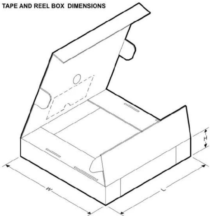
TAPE AND REEL BOX DIMENSIONS W L*All dimensions are nominal
| Device | Package Type | Package Drawing | Pins | SPQ | Length (mm) | Width (mm) | Height (mm) |
| OPA209AIDBVR SOT | 23 DBV 5 3000 223.0 | 270.0 35.0 | |||||
| OPA209AIDBVT SOT | 23 DBV 5 250 223.0 | 270.0 35.0 | |||||
| OPA209AIDR | SOIC | D | 8 | 2500 | 853.0 | 449.0 | 35.0 |
| OPA2209AIDGKR VSS | OP DGK | 8 2500 853.0 449.0 | 35.0 | ||||
| OPA2209AIDGKT VSS | OP DGK | 8 250 210.0 185.0 | 35.0 | ||||
| OPA2209AIDR | SOIC | D | 8 | 2500 | 853.0 | 449.0 | 35.0 |
| OPA4209AIPWR | TSSOP | PW | 14 | 2000 | 853.0 | 449.0 | 35.0 |
TUBE
text_image
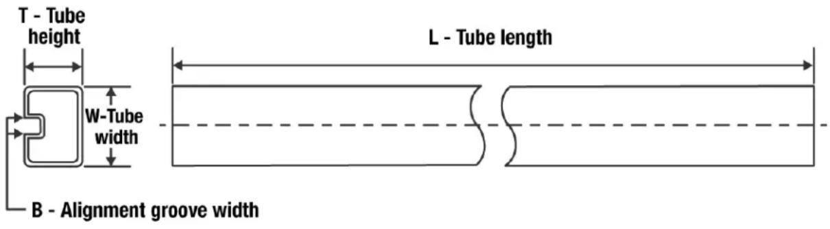
T - Tube height W-Tube width L - Tube length B - Alignment groove width*All dimensions are nominal
| Device | Package Name | Package Type | Pins | SPQ | L (mm) | W (mm) | T (μm) | B (mm) |
| OPA209AID D SOIC | 8 75 506.6 8 3940 | 4.32 | ||||||
| OPA2209AID D SOIC | 8 75 506.6 8 3940 | 4.32 | ||||||
| OPA4209AIPW PW T | SSOP 14 90 530 10 | 2 3600 | 3.5 |
SMALL OUTLINE TRANSISTOR
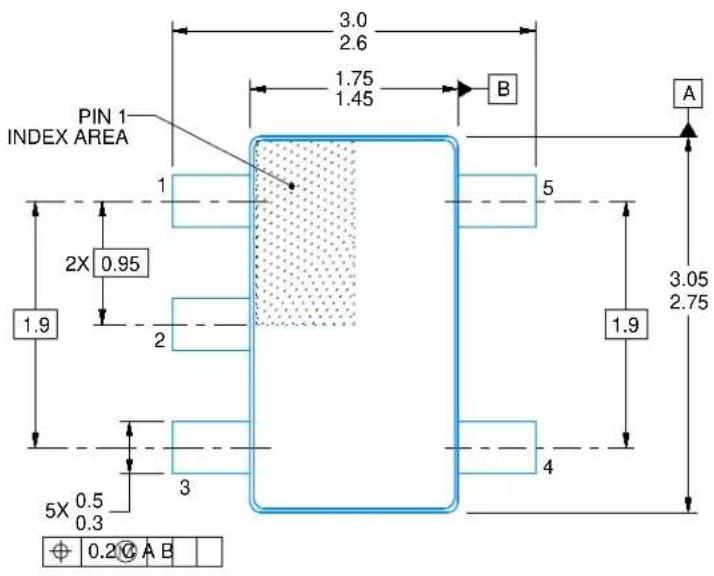
text_image
PIN 1 INDEX AREA 2X 0.95 1.9 5X 0.5 0.3 3 1.75 1.45 B 5 1.9 4 3.05 2.75 A 0.2 A B
text_image
C 0.1 C 1.45 0.90 (1.1) 0.15 TYP 0.00
text_image
0.25 GAGE PLANE 8° TYP 0° 0.6 TYP 0.3 SEATING PLANE 0.22 TYP 0.084214839/F 06/2021
NOTES:
- All linear dimensions are in millimeters. Any dimensions in parenthesis are for reference only. Dimensioning and tolerancing per ASME Y14.5M.
- This drawing is subject to change without notice.
- Reference JEDEC MO-178.
- Body dimensions do not include mold flash, protrusions, or gate burrs. Mold flash, protrusions, or gate burrs shall not exceed 0.25 mm per side.
SMALL OUTLINE TRANSISTOR
text_image
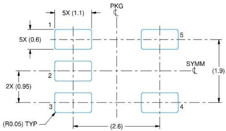
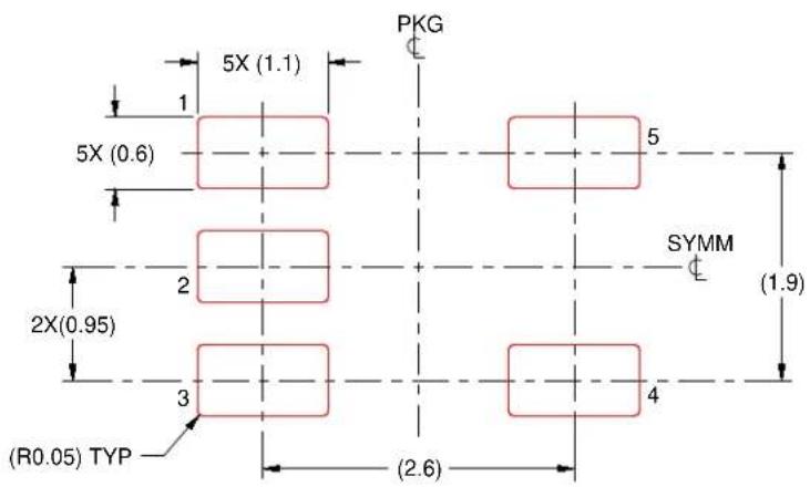
5X (1.1) PKG 1 5X (0.6) 2 2X (0.95) 3 (R0.05) TYP (2.6) 4 SYMM (1.9)LAND PATTERN EXAMPLE
EXPOSED METAL SHOWN
SCALE:15X
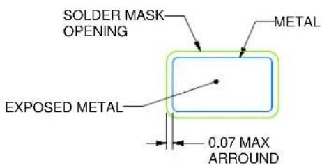
text_image
SOLDER MASK OPENING METAL EXPOSED METAL 0.07 MAX ARROUNDNON SOLDER MASK
DEFINED
(PREFERRED)
text_image
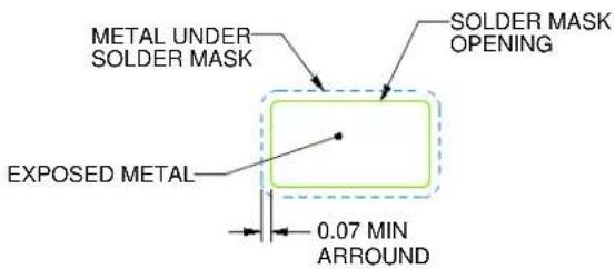
METAL UNDER SOLDER MASK SOLDER MASK OPENING EXPOSED METAL 0.07 MIN ARROUNDSOLDER MASK
DEFINED
SOLDER MASK DETAILS
4214839/F 06/2021
NOTES: (continued)
- Publication IPC-7351 may have alternate designs.
- Solder mask tolerances between and around signal pads can vary based on board fabrication site.
SMALL OUTLINE TRANSISTOR
text_image
5X (1.1) 1 5X (0.6) 2 2X(0.95) 3 (R0.05) TYP PKG 5 SYMM (1.9) (2.6)SOLDER PASTE EXAMPLE BASED ON 0.125 mm THICK STENCIL SCALE:15X
4214839/F 06/2021
NOTES: (continued)
- Laser cutting apertures with trapezoidal walls and rounded corners may offer better paste release. IPC-7525 may have alternate design recommendations.
- Board assembly site may have different recommendations for stencil design.
PW (R-PDSO-G14)
NOTES: A. All linear dimensions are in millimeters. Dimensioning and tolerancing per ASME Y14.5M-1994.
B. This drawing is subject to change without notice.
Body length does not include mold flash, protrusions, or gate burrs. Mold flash, protrusions, or gate burrs shall not exceed 0.15 each side.
Body width does not include interlead flash. Interlead flash shall not exceed 0,25 each side.
E. Falls within JEDEC MO-153
PW (R-PDSO-G14)
A. All linear dimensions are in millimeters.
B. This drawing is subject to change without notice.
C. Publication IPC-7351 is recommended for alternate designs.
D. Laser cutting apertures with trapezoidal walls and also rounding corners will offer better paste release. Customers should contact their board assembly site for stencil design recommendations. Refer to IPC-7525 for other stencil recommendations.
E. Customers should contact their board fabrication site for solder mask tolerances between and around signal pads.
SMALL OUTLINE INTEGRATED CIRCUIT

4214825/C 02/2019
NOTES:
- Linear dimensions are in inches [millimeters]. Dimensions in parenthesis are for reference only. Controlling dimensions are in inches. Dimensioning and tolerancing per ASME Y14.5M.
- This drawing is subject to change without notice.
- This dimension does not include mold flash, protrusions, or gate burrs. Mold flash, protrusions, or gate burrs shall not exceed .006 [0.15] per side.
- This dimension does not include interlead flash.
- Reference JEDEC registration MS-012, variation AA.
SMALL OUTLINE INTEGRATED CIRCUIT
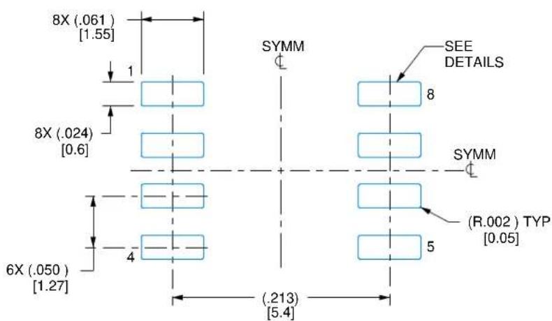
text_image
8X (.061) [1.55] 1 8X (.024) [0.6] 6X (.050) [1.27] 4 (.213) [5.4] SYMM SEE DETAILS 8 SYMM (R.002) TYP [0.05]LAND PATTERN EXAMPLE EXPOSED METAL SHOWN SCALE:8X
text_image
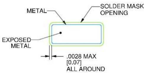
METAL SOLDER MASK OPENING EXPOSED METAL .0028 MAX [0.07] ALL AROUNDNON SOLDER MASK DEFINED

text_image
SOLDER MASK OPENING METAL UNDER SOLDER MASK EXPOSED METAL .0028 MIN [0.07] ALL AROUNDSOLDER MASK
DEFINED
SOLDER MASK DETAILS
4214825/C 02/2019
NOTES: (continued)
- Publication IPC-7351 may have alternate designs.
- Solder mask tolerances between and around signal pads can vary based on board fabrication site.
SMALL OUTLINE INTEGRATED CIRCUIT

text_image
8X (.061) [1.55] 1 8X (.024) [0.6] 6X (.050) [1.27] 4 (.213) [5.4] SYMM 8 SYMM (R.002) TYP [0.05]SOLDER PASTE EXAMPLE BASED ON .005 INCH [0.125 MM] THICK STENCIL SCALE:8X
4214825/C 02/2019
NOTES: (continued)
- Laser cutting apertures with trapezoidal walls and rounded corners may offer better paste release. IPC-7525 may have alternate design recommendations.
- Board assembly site may have different recommendations for stencil design.
DGK (S-PDSO-G8)
PLASTIC SMALL-OUTLINE PACKAGE

4073329/E 05/06
NOTES: A. All linear dimensions are in millimeters.
B. This drawing is subject to change without notice.
C Body length does not include mold flash, protrusions, or gate burrs. Mold flash, protrusions, or gate burrs shall not exceed 0.15 per end.
D> Body width does not include interlead flash. Interlead flash shall not exceed 0.50 per side.
E. Falls within JEDEC MO-187 variation AA, except interlead flash.
DGK (S-PDSO-G8)
Example Board Layout
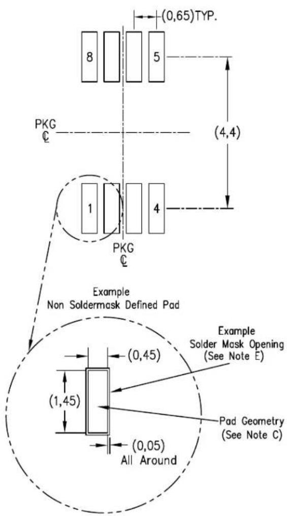
text_image
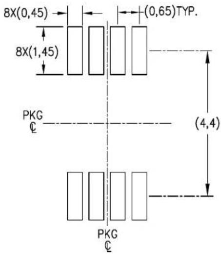
(0,65)TYP. 8 5 PKG C (4,4) 1 4 PKG C Example Non Soldermask Defined Pad Example Solder Mask Opening (See Note E) (0,45) (1,45) Pad Geometry (See Note C) (0,05) All AroundExample Stencil Openings
Based on a stencil thickness of .127mm (.005inch).
(See Note D)
text_image
8X(0,45) 8X(1,45) (0,65)TYP. PKG C (4,4) PKG C4221236/A 11/13
NOTES: A. All linear dimensions are in millimeters.
B. This drawing is subject to change without notice.
C. Publication IPC-7351 is recommended for alternate designs.
D. Laser cutting apertures with trapezoidal walls and also rounding corners will offer better paste release. Customers should contact their board assembly site for stencil design recommendations. Refer to IPC-7525 for other stencil recommendations.
E. Customers should contact their board fabrication site for solder mask tolerances between and around signal pads.
IMPORTANT NOTICE AND DISCLAIMER
TI PROVIDES TECHNICAL AND RELIABILITY DATA (INCLUDING DATA SHEETS), DESIGN RESOURCES (INCLUDING REFERENCE DESIGNS), APPLICATION OR OTHER DESIGN ADVICE, WEB TOOLS, SAFETY INFORMATION, AND OTHER RESOURCES "AS IS" AND WITH ALL FAULTS, AND DISCLAIMS ALL WARRANTIES, EXPRESS AND IMPLIED, INCLUDING WITHOUT LIMITATION ANY IMPLIED WARRANTIES OF MERCHANTABILITY, FITNESS FOR A PARTICULAR PURPOSE OR NON-INFRINGEMENT OF THIRD PARTY INTELLECTUAL PROPERTY RIGHTS.
These resources are intended for skilled developers designing with TI products. You are solely responsible for (1) selecting the appropriate TI products for your application, (2) designing, validating and testing your application, and (3) ensuring your application meets applicable standards, and any other safety, security, regulatory or other requirements.
These resources are subject to change without notice. TI grants you permission to use these resources only for development of an application that uses the TI products described in the resource. Other reproduction and display of these resources is prohibited. No license is granted to any other TI intellectual property right or to any third party intellectual property right. TI disclaims responsibility for, and you will fully indemnify TI and its representatives against, any claims, damages, costs, losses, and liabilities arising out of your use of these resources.
TI's products are provided subject to TI's Terms of Sale or other applicable terms available either on ti.com or provided in conjunction with such TI products. TI's provision of these resources does not expand or otherwise alter TI's applicable warranties or warranty disclaimers for TI products.
TI objects to and rejects any additional or different terms you may have proposed.
Mailing Address: Texas Instruments, Post Office Box 655303, Dallas, Texas 75265
Copyright © 2022, Texas Instruments Incorporated