LM8261M5X/NOPB - Electronic component TEXAS INSTRUMENTS - Free user manual and instructions
Find the device manual for free LM8261M5X/NOPB TEXAS INSTRUMENTS in PDF.

User questions about LM8261M5X/NOPB TEXAS INSTRUMENTS
0 question about this device. Answer the ones you know or ask your own.
Ask a new question about this device
Download the instructions for your Electronic component in PDF format for free! Find your manual LM8261M5X/NOPB - TEXAS INSTRUMENTS and take your electronic device back in hand. On this page are published all the documents necessary for the use of your device. LM8261M5X/NOPB by TEXAS INSTRUMENTS.
USER MANUAL LM8261M5X/NOPB TEXAS INSTRUMENTS
LM8261SingleRRIOHighOutputCurrent&UnlimitedCapLoadOpAmp
1Features3Description
- (V_S = 5V, T_A = 25^, TypicalValuesUnless Specified)
•GBWP21MHz
•WideSupplyVoltageRange2.5Vto30V
•SlewRate12V/μs
•SupplyCurrent0.97mA - CapLoadLimitUnlimited
• OutputShortCircuitCurrent53mA/-75mA - ±5%SettlingTime400ns(500pF,100mV Step) PP
- InputCommonModeVoltage0.3VBeyondRails
- InputVoltageNoise15nV/√Hz
- InputCurrentNoise1pA/√Hz
- THD+N<0.05%
2Applications
•TFT-LCDFlatPanelV COM Driver
•A/DConverterBuffer
•HighSide/lowSideSensing
•HeadphoneAmplifier
TheLM8261isaRail-to-RailinputandoutputOp Ampwhichcanoperatewithawidesupplyvoltage range. This device hashhighoutputcurrentdrive, greater than Rail-to-Railinputcommonmodevoltage range, unlimited capacitiveloaddrive capability, and provided tested and guaranteed high speed and slew rate while requiring only 0.97 mA supply current. It is specifically designed to handle the requirements of flat panel TFT panel V COM driver applications as well as being suitable for other low power, and medium speed applications which require ease of use and enhanced performance over existing devices.
Greater than Rail-to-Rail input common mode voltage rangewith 50 dB of Common Mode Rejection allows high side and low side sensing, among many applications, without concern over exceeding the range and with no compromise in accuracy.
Exceptionally wide operating supply voltage range of 2.5 V to 30 V alleviates any concerns over functionality under extreme conditions and offers flexibility for use in multitude of applications. In addition, most device parameters are insensitive to powersupplyvariations;thisdesignenhancementis yetanotherstepinsimplifyingitsusage.Theoutput stagehaslowdistortion(0.05%THD+N)andcan supply a respectable amount of current (15 mA) with minimalheadroomfromeitherrail(300mV).
TheLM8261 is offered in the space-saving SOT-23-5 package.
DeviceInformation (1)
| PART NUMBER | PACKAGE | BODY SIZE (NOM) |
| LM8261 | SOT-23 (5) | 2.9 mm × 1.6 mm |
(1) For all available packages, see the orderable addendum at the end of the data sheet.
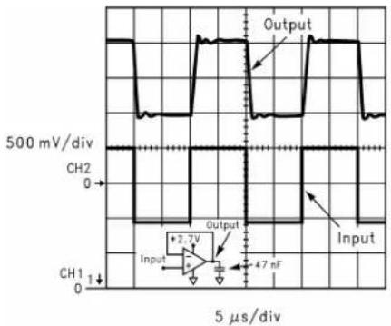
OutputResponsewithHeavyCapacitiveLoad
line
| Time (μs) | Output (mV) | Input (nF) | |-----------|-------------|------------| | 0 | 500 | 0 | | 500 | 500 | 0 | | 1000 | 500 | 0 | | 1500 | 500 | 0 | | 2000 | 500 | 0 | | 2500 | 500 | 0 | | 3000 | 500 | 0 | | 3500 | 500 | 0 | | 4000 | 500 | 0 | | 4500 | 500 | 0 | | 500 | 500 | 0 | | 550 | 500 | 0 | | 600 | 500 | 0 | | 650 | 500 | 0 | | 700 | 500 | 0 | | 750 | 500 | 0 | | 800 | 500 | 0 | | 850 | 500 | 0 | | 900 | 500 | 0 | | 950 | 500 | 0 | | 1000 | 500 | 0 | | 1050 | 500 | 0 | | 1100 | 500 | 0 | | 1150 | 500 | 0 | | 1200 | 500 | 0 | | 1250 | 500 | 0 | | 1300 | 500 | 0 | | 1350 | 500 | 0 | | 1400 | 500 | 0 | | 1450 | 500 | 0 | | 1500 | 500 | 0 | | 1550 | 500 | 0 | | 1600 | 500 | 0 | | 1650 | 500 | 0 | | 1700 | 500 | 0 | | 1750 | 500 | 0 | | 1800 | 500 | 0 | | 1850 | 500 | 0 | | 1900 | 500 | 0 | | 1950 | 500 | 0 | | 2000 | 500 | 0 | | 2050 | 500 | 2.7 | | 2100 | 500 | +2.7 | | 2150 | 500 | +2.7 | | 2200 | 500 | +2.7 | | 2250 | 500 | +2.7 | | 2300 | 500 | +2.7 | | 2350 | 500 | +2.7 | | 2400 | 500 | +2.7 | | 2450 | 500 | +2.7 | | 2500 | 500 | +2.7 | | 2550 | 500 | +2.7 | | 2600 | 500 | +2.7 | | 2650 | 500 | +2.7 | | 2700 | 500 | +2.7 | | 2750 | 500 | +2.7 | | 2800 | 500 | +2.7 | | 2850 | 500 | +2.7 | | 2900 | 500 | +2.7 | | 2950 | 500 | +2.7 | | 3833 | - | - | | Note: The output values are not provided in the code. The input values are labeled as 'Input' and 'Output'. The data is presented in a format format for visualization purposes. There is only one data series in this case.TableofContents
1 Features.... 1
2 Applications 1
3 Description 1
4 Revision History...... 2
5PinConfigurationandFunctions....3
6 Specifications.... 4
6.1 AbsoluteMaximumRatings....4
6.2ESDRatings....4
6.3RecommendedOperatingConditions....4
6.4ThermalInformation....4
6.5 Electrical Characteristics 2.7V....5
6.6 Electrical Characteristics5V....7
6.7 Electrical Characteristics±15V....9
6.8TypicalCharacteristics....11
7ApplicationandImplementation....19
7.1 BlockDiagramandOperationalDescription....19
7.2DrivingCapacitiveLoads....20
7.3EstimatingtheOutputVoltageSwing....22
7.4TFTApplications....23
7.5 Output Short Circuit Current and Dissipation Issues....23
7.6OtherApplicationHints....24
8PowerSupplyRecommendations....25
9 Layout 25
9.1 LayoutGuidelines....25
9.2LayoutExample....26
10DeviceandDocumentationSupport......27
10.1 DocumentationSupport....27
10.2Trademarks....27
10.3ElectrostaticDischargeCaution....27
10.4Glossary....27
11Mechanical, Packaging, and Orderable Information 27
4RevisionHistory
ChangesfromRevisionl(March2013)toRevisionJPage
- Added, updated, or revised the following sections: Pin Configuration and Functions, Specifications, Detailed Description, Application and Implementation, Power Supply Recommendations, Layout, Device and Documentation Support, and Mechanical, Packaging, and Orderable Information section .... 1
- Changed from -1.0 V to -0.8 V in Specifications 4
ChangesfromRevisionH(March2013)toRevisionI
Page
- Changed layout of National Data Sheet to TI format .... 1
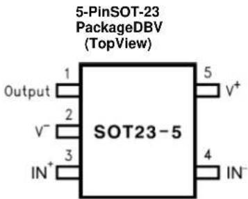
5PinConfigurationandFunctions
text_image
5-PinSOT-23 PackageDBV (TopView) Output 1 5 V+ 2 SOT23-5 V- 3 4 IN- IN+PinFunctions
| PIN | I/ODESCRIPTION | |
| NUMBERNAME | ||
| 1OutputOOutput | ||
| 2V-INegativeSupply | ||
| 3IN+ | INon-invertinginput | |
| 4 | IN- | InvertingInput |
| 5 | V+ | IPositiveSupply |
6Specifications
6.1 AbsoluteMaximumRatings (1)
| MINMAXUNIT | |||
| V_IN Differential±10V | |||
| OutputShortCircuitDurationSee | (2)(3) | ||
| SupplyVoltage( V^+ - V^- )32V | |||
| VoltageatInput/OutputpinsV | V^+ + 0.8V, V^- - 0.8V | ||
| StorageTemperatureRange-65 +150 °C | |||
| JunctionTemperature (4) | 150 | °C | |
| SolderingInformation: | InfraredorConvection(20sec.) | 235 | °C |
| WaveSoldering(10sec.) | 260 | °C | |
(1) Absolute Maximum Ratings indicate limits beyond which damage to the device may occur. Operating Rating indicate conditions for which the device is intended to be functional, but specific performance is not guaranteed. For guaranteed specifications and the test conditions, see ElectricalCharacteristics2.7V.
(2) Applies to both single-supply and split-supply operation. Continuous short circuit operation at elevated ambient temperature can result in exceeding them maximum allowed junction temperature of 150^ C.
(3) AllowableOutputShortCircuitdurationisinfiniteforV S ≤ 6V Vatroomtemperatureandbelow.ForV S >6V ,allowableshortcircuitdurationis1.5ms.
(4) Themaximumpowerdissipationisafunctionof T_J() , R_ JA , and T_A . The maximum allowable powerdissipation at any ambient temperature is P_D = (T_J() - T_A)/R_ JA . All numbers apply for packagessoldered directly onto a PC board.
6.2ESDRatings
| VALUE | UNIT | ||
| V_(ESD) Electrostaticdischarge | Human-bodymodel(HBM),perANSI/ESDA/JEDECJS-001 (1)(2) | ±2000 | V |
| Machinemodel(MM) (3) | ±200 | ||
(1) JEDEC document JEP155 states that 500-V HBM allows safe manufacturing with a standard ESD control process. Manufacturing with less than 2000-V HBM is possible with the necessary precautions. Pins listed as ±200 V may actually have higher performance.
(2) HumanBodyModelis1.5kΩ inserieswith100pF.
(3) MachineModel,0Ω isserieswith200pF.
6.3 Recommended Operating Conditions
| MINMAX | UNIT | ||
| SupplyVoltage(V + - V-) | 2.530 | V | |
| TemperatureRange (1) | -40 | +85 | °C |
(1) Themaximumpowerdissipationisafunctionof T_J() , R_ JA , and T_A . The maximum allowable powerdissipation at any ambient temperature is P_D = (T_J() - T_A)/R_ JA . All numbers apply for packagessoldered directly onto a PC board.
6.4ThermalInformation
| THERMALMETRIC (1)(2) | DBV | UNIT | |
| (5PINS) | |||
| R_ JA | Junction-to-ambientthermalresistance | 325 | °C/W |
(1) For more information about traditional and new thermal metrics, see the IC Package Thermal Metrics application report, SPRA953.
(2) ThemaximumpowerdissipationisafunctionofT J() , R JA , and T A .Themaximumallowablepowerdissipationatanyambient temperatureisP D = (T J(MAX) - T A )/ R _ JA .AllnumbersapplyforpackagessoldereddirectlyontoaPCboard.
6.5 Electrical Characteristics2.7V
Unless otherwise specified, all limits guaranteed for T to V ^- . ^(1) A = 25°C, V ^+ = 2.7V, V ^- = 0V, V CM = 0.5V, V O = V ^+ /2, and R _L >1MΩ
| PARAMETERTEST CONDITIONSMINTYP | (2) MAX(3) | UNIT | ||||
| V_OS | InputOffsetVoltageV | CM=0.5V\&V_CM=2.2VmV | +/-0.7+/-5 | |||
| -65°C≤ J≤ +150°C+/-7 | ||||||
| TC V_OS | InputOffsetAverageDriftV | CM=0.5V\&V_CM=2.2V^(4) | +/-2μV/C | |||
| I_B | InputBiasCurrent | V_CM=0.5V^(5) | -1.20 -2.00 | μA | ||
| -65°C≤ J≤ +150°C | -2.70 | |||||
| V_CM=2.2V^(5) | +0.49 +1.00 | |||||
| -65°C≤ J≤ +150°C | +1.60 | |||||
| I_OS | InputOffsetCurrent | V_CM=0.5V\&V_CM=2.2V | 20 250 | nA | ||
| -65°C≤ J≤ +150°C | 400 | |||||
| CMRR | CommonModeRejection Ratio | V_CM steppedfrom 0Vto1.0V | 100 76 | dB | ||
| -65°C≤ J≤ +150°C | 60 | |||||
| V_CM steppedfrom1.7Vto2.7V | 100 | |||||
| V_CM steppedfrom 0Vto2.7V | 70 58 | |||||
| -65°C≤ J≤ +150°C | 50 | |||||
| +PSRR | PositivePowerSupply RejectionRatio | V^+=2.7Vto5V | 104 78 | dB | ||
| -65°C≤ J≤ +150°C | 74 | |||||
| CMVR | InputCommon-Mode VoltageRange | CMRR>50dB | -0.3 -0.1 | V | ||
| -65°C≤ J≤ +150°C | 0.0 | |||||
| 3.0 2.8 | V | |||||
| -65°C≤ J≤ +150°C | 2.7 | |||||
| A_VOL | LargeSignalVoltageGain | V_O=0.5to2.2V, R_L=10KtoV^- | 78 70 | dB | ||
| -65°C≤ J≤ +150°C | 67 | |||||
| V_O=0.5to2.2V, R_L=2KtoV^- | 73 67 | dB | ||||
| -65°C≤ J≤ +150°C | 63 | |||||
| V_O | OutputSwingHigh | R_L=10KtoV^- | 2.59 2.49 | V | ||
| -65°C≤ J≤ +150°C | 2.46 | |||||
| R_L=2KtoV^- | 2.53 2.45 | |||||
| -65°C≤ J≤ +150°C | 2.41 | |||||
| OutputSwingLow | R_L=10KtoV^- | 90 100 | mV | |||
| -65°C≤ J≤ +150°C | 120 | |||||
| I_SC | OutputShortCircuitCurrent | SourcingtoV - V_ID=200mV^(6)(7) | 48 30 | mA | ||
| -65°C≤ J≤ +150°C | 20 | |||||
| SinkingtoV + V_ID=-200mV^(6)(7) | 65 50 | mA | ||||
| -65°C≤ J≤ +150°C | 30 | |||||
(1) Electrical Table values apply only for factory testing conditions at the temperature indicated. Factory testing conditions result in very limited self-heating of the device such that TJ = TA. No guarantee of parametric performance is indicated in the electrical tables under conditionsofinternalselfheatingwhereTJ>TA.
(2) TypicalValuesrepresentthemostlikelyparametricnorm.
(3) Alllimitsareguaranteedbytestingorstatisticalanalysis.
(4) Offset voltage average drift determined by dividing the change in VOS at temperature extremes into the total temperature change.
(5) Positivecurrentcorrespondstocurrentflowingintothedevice.
(6) ProductionShortCircuittestisamomentarytest.SeeNote7.
(7) Allowable Output Short Circuit duration is infinite for VS ≤ 6V at room temperature and below. For VS > 6V, allowable short circuit duration is 1.5ms.
ElectricalCharacteristics2.7V(continued)
Unless otherwise specified, all limits guaranteed for T to V ^- . (1)
| PARAMETERTEST | CONDITIONSMINTYP | (2) MAX(3) | UNIT | ||
| I_S SupplyCurrentmA | Noload, V_CM = 0.5V | 0.951.20 | |||
| -65°C≤ J ≤ +150°C1.50 | |||||
| SRSlewRate (8) | A_V =+1,V_I=2V_PP | 9V/μs | |||
| f_u UnityGain-FrequencyV | _I=10mV,R_L=2K toV+/210MHz | ||||
| GBWP Gain Bandwidth Product | f = 50 KHz | 2115.5 | MHz | ||
| -65°C≤ J ≤ +150°C14 | |||||
| Phi_m PhaseMargin | V_I=10mV | 50 | Deg | ||
| e_n Input-ReferredVoltage Noise | f=2KHz, R_S=50 | 15 | nV/√Hz | ||
| i_n Input-ReferredCurrent Noise | f=2KHz | 1 | pA/√Hz— | ||
| f_MAX FullPowerBandwidth | Z_L=(20pF||10K)toV^+/2 | 1MHz | |||
(8) Slew rate is the slower of the rising and falling slew rates. Connected as a Voltage Follower.
6.6 Electrical Characteristics5V (1)
Unless otherwise specified, all limited guaranteed for T A=25^,V^+=5V,V^-=0V,VCM=1V,V_O=V^+/2 , and R_L>1M to V^- .
| PARAMETERTESTCONDITIONS MINTYP | (2) MAX(3) | UNIT | ||||
| V_OS | InputOffsetVoltageV | =1V&V\=4.5Vm | +/-0.7+/-5 | |||
| -65°C≤ J≤ +150°C+/- 7 | ||||||
| TC V_OS | InputOffsetAverageDriftV | =1V&V\=4.5V (4) | +/-2μV/°C | |||
| I_B | InputBiasCurrent | V_CM=1V^(5) | -1.18 -2.00 | μA | ||
| -65°C≤ J≤ +150°C | -2.70 | |||||
| V_CM=4.5V^(5) | +0.49 +1.00 | |||||
| -65°C≤ J≤ +150°C | +1.60 | |||||
| I_OS | InputOffsetCurrent | V_CM=1V&V\=4.5V | 20 250 | nA | ||
| -65°C≤ J≤ +150°C | 400 | |||||
| CMRR | CommonModeRejectionRatio | V_CM steppedfrom 0Vto3.3V | 110 84 | dB | ||
| -65°C≤ J≤ +150°C | 72 | |||||
| V_CM steppedfrom 4Vto5V | 100 | |||||
| V_CM steppedfrom 0Vto5V | 80 64 | |||||
| -65°C≤ J≤ +150°C | 61 | |||||
| +PSRR | PositivePowerSupplyRejection Ratio | V_CM^+=2.7Vto5V,V_CM=0.5V | 104 78 | dB | ||
| -65°C≤ J≤ +150°C | 74 | |||||
| CMVR | InputCommon-ModeVoltage Range | CMRR>50dB | -0.3-0.1 | V | ||
| -65°C≤ J≤ +150°C | 0.0 | |||||
| 5.3 5.1 | V | |||||
| -65°C≤ J≤ +150°C | 5.0 | |||||
| A_VOL | LargeSignalVoltageGain | V_O=0.5to4.5V,R_L=10KtoV | 84 74 | dB | ||
| -65°C≤ J≤ +150°C | 70 | |||||
| V_O=0.5to4.5V,R_L=2KtoV | 80 70 | |||||
| -65°C≤ J≤ +150°C | 66 | |||||
| V_O | OutputSwingHigh | R_L=10KtoV | 4.87 4.75 | V | ||
| -65°C≤ J≤ +150°C | 4.72 | |||||
| R_L=2KtoV | 4.81 4.70 | |||||
| -65°C≤ J≤ +150°C | 4.66 | |||||
| OutputSwingLow | R_L=10KtoV | 86 125 | mV | |||
| -65°C≤ J≤ +150°C | 135 | |||||
| I_SC | OutputShortCircuitCurrent | SourcingtoV- V_ID=200mV^(6)(7) | 53 35 | mA | ||
| -65°C≤ J≤ +150°C | 20 | |||||
| SinkingtoV+ V_ID=-200mV^(6)(7) | 75 60 | |||||
| -65°C≤ J≤ +150°C | 50 | |||||
(1) Electrical Table values apply only for factory testing conditions at the temperature indicated. Factory testing conditions result in very limited self-heating of the device such that TJ = TA. No guarantee of parametric performance is indicated in the electrical tables under conditionsofinternalselfheatingwhereTJ>TA.
(2) TypicalValuesrepresentthemostlikelyparametricnorm.
(3) Alllimitsareguaranteedbytestingorstatisticalanalysis.
(4) Offset voltage average drift determined by dividing the change in VOS at temperature extremes into the total temperature change.
(5) Positivecurrentcorrespondstocurrentflowingintothedevice.
(6) ProductionShortCircuittestisamomentarytest.SeeNote7.
(7) Allowable Output Short Circuit duration is infinite for VS ≤ 6V at room temperature and below. For VS > 6V, allowable short circuit duration is 1.5ms.
ElectricalCharacteristics5V ^(1) (continued)
Unless otherwise specified, all limited guaranteed for T A=25^ , V^+=5V , V^-=0V , VCM=1V , V_O=V^+/2 , and R_L>1M to V^- .
| PARAMETERTESTCONDITIONSMINTYP | (2) MAX(3) | UNIT | |||
| I_S SupplyCurrentNoload,V | cm=1VmA | 0.971.25 | |||
| -65°C≤ J≤ +150°C1.75 | |||||
| SRSlewRate^(8) | A_V=+1,V_I=5V_PP | 1210 | V/μs | ||
| -65°C≤ J≤ +150°C7 | |||||
| f_u UnityGainFrequency | V_I=10mV,R_L=2KΩ toV^+/2 | 10.5 | MHz | ||
| GBWP Gain-Bandwidth Product | f = 50 KHz | 2116 | MHz | ||
| -65°C≤ J≤ +150°C | 15 | ||||
| Phi_m PhaseMargin | V_I=10mV | 53 | Deg | ||
| e_n Input-ReferredVoltageNoise | f=2KHz,R_S=50 Ω | 15 | nV/ | ||
| i_n Input-Referred Current Noise | f = 2 KHz | 1 | pA/ | ||
| f_MAX FullPowerBandwidth | Z_L=(20pF||10kΩ)toV ^+/2 | 900 | KHz | ||
| t_S SettlingTime(±5%) | 100mV PP Step,500pFloat | 400 | ns | ||
| THD+N | TotalHarmonicDistortion+ Noise | R_L=1KΩ toV^+/2f=10KHztoA _V=+2,4V_PP swing | 0.05% | ||
(8) Slew rate is the slower of the rising and falling slew rates. Connected as a Voltage Follower.
6.7 ElectricalCharacteristics±15V (1)
Unless otherwise specified, all limited guaranteed for T to 0V. A = 25^,V^+ = 15V,V^- = -15V,VCM = 0V,VO = 0V, and _L > 1M
| PARAMETERTESTCONDITIONS MINTYP | (2) MAX(3) | UNIT | ||||
| V_OS | InputOffsetVoltagemV | V_CM=-14.5V&V CM=14.5V | +/-0.7+/-7 | |||
| -65°C≤ J≤ +150°C+/- | 9 | |||||
| TC V_OS | InputOffsetAverageDriftV | CM=-14.5V&V CM=14.5V^(4) | +/-2μV/°C | |||
| I_B | InputBiasCurrent | V_CM=-14.5V^(5) | -1.05 | -2.00 | μA | |
| -65°C≤ J≤ +150°C | -2.80 | |||||
| V_CM=14.5V^(5) | +0.49 | +1.00 | ||||
| -65°C≤ J≤ +150°C | +1.50 | |||||
| I_OS | InputOffsetCurrent | V_CM=-14.5V&V CM=14.5V | 30 | 275 | nA | |
| -65°C≤ J≤ +150°C | 550 | |||||
| CMRR | CommonModeRejectionRatio | V_CM steppedfrom-15V to13V | 100 | 84 | dB | |
| -65°C≤ J≤ +150°C | 80 | |||||
| CM steppedfrom14Vto15V | 100 | |||||
| V_CM steppedfrom-15V to15V | 88 | 74 | ||||
| -65°C≤ J≤ +150°C | 72 | |||||
| +PSRR | PositivePowerSupplyRejection Ratio | V^+=12Vto15V | 100 | 70 | dB | |
| -65°C≤ J≤ +150°C | 66 | |||||
| -PSRR | NegativePowerSupplyRejection Ratio | V^-=-12Vto-15V | 100 | 70 | dB | |
| -65°C≤ J≤ +150°C | 66 | |||||
| CMVR | InputCommon-ModeVoltage Range | CMRR>50dB | -15.3 | -15.1 | V | |
| -65°C≤ J≤ +150°C | -15.0 | |||||
| 15.3 | 15.1 | V | ||||
| -65°C≤ J≤ +150°C | 15.0 | |||||
| A_VOL | LargeSignalVoltageGain | V_O=0Vto±13V, R_L=10KΩ | 85 | 78 | dB | |
| -65°C≤ J≤ +150°C | 74 | |||||
| V_O=0Vto±13V, R_L=2KΩ | 79 | 72 | ||||
| -65°C≤ J≤ +150°C | 66 | |||||
| V_O | OutputSwingHigh | R_L=10KΩ | 14.83 | 14.65 | V | |
| -65°C≤ J≤ +150°C14.61 | ||||||
| R_L=2KΩ | 14.73 | 14.60 | ||||
| -65°C≤ J≤ +150°C14.55 | ||||||
| OutputSwingLow | R_L=10KΩ | -14.91 | -14.75 | V | ||
| -65°C≤ J≤ +150°C | -14.65 | |||||
| R_L=2KΩ | -14.83 | -14.65 | ||||
| -65°C≤ J≤ +150°C | -14.60 | |||||
| I_SC | OutputShortCircuitCurrent | Sourcingoground V_ID=200mV^(6)(7) | 60 | 40 | mA | |
| -65°C≤ J≤ +150°C | 25 | |||||
| Sinkingoground V_ID=200mV^(6)(7) | 100 | 70 | ||||
| -65°C≤ J≤ +150°C | 60 | |||||
(1) Electrical Table values apply only for factory testing conditions at the temperature indicated. Factory testing conditions result in very limitedself-heatingofthedevicesuchthatT J=TA .Noguaranteeofparametricperformanceisindicatedintheelectricaltablesunder conditionsofinternalselfheatingwhereT J>TA .
(2) TypicalValuesrepresentthemostlikelyparametricnorm.
(3) Alllimitsareguaranteedbytestingorstatisticalanalysis.
(4) OffsetvoltageaveragedriftdeterminedbydividingthechangeinV OS attemperatureextremesintothetotaltemperaturechange.
(5) Positivecurrentcorrespondstocurrentflowingintothedevice.
(6) ProductionShortCircuittestisamomentarytest.SeeNote7.
(7) AllowableOutputShortCircuitdurationisinfiniteforV S ≤ 6V Vatroomtemperatureandbelow. For V S >6V , allowableshortcircuit durationis1.5ms.
ElectricalCharacteristics±15V (1) (continued)
Unless otherwise specified, all limited guaranteed for T to 0V.
| PARAMETERTESTCONDITIONSMINTYP | (2) MAX(3) | UNIT | |||
| I_S SupplyCurrentNoload,V | CM=0VmA | 1.301.50 | |||
| -65°C≤ J≤ +150°C1.90 | |||||
| SRSlewRate (8) | A_V=+1,V_I=24V_PP | 1510 | V/μs | ||
| -65°C≤ J≤ +150°C8 | |||||
| f_u UnityGainFrequency | V_I=10mV,R_L=2KΩ | 14 | MHz | ||
| GBWP Gain-Bandwidth Product | f = 50 KHz | 2418 | MHz | ||
| -65°C≤ J≤ +150°C | 16 | ||||
| Phi_m PhaseMargin | V_I=10mV | 58 | Deg | ||
| e_n Input-ReferredVoltageNoise | f=2KHz, R_S=50Ω | 15 | nV/ | ||
| i_n Input-Referred Current Noise | f = 2 KHz | 1 | pA/ | ||
| f_MAX FullPowerBandwidth | Z_L=20pF||10KΩ | 160 | KHz | ||
| t_s SettlingTime( ± 1% , A_V=+1 ) | PositiveStep,5V PP | 320 | ns | ||
| NegativeStep,5V PP | 600 | ||||
| THD+N TotalHarmonicDistortion+Noise | R_L=1KΩ,f=10KHz,A_V=+2,28V_PP swing | 0.01% | |||
(8) Slew rate is the slower of the rising and falling slew rates. Connected as a Voltage Follower.
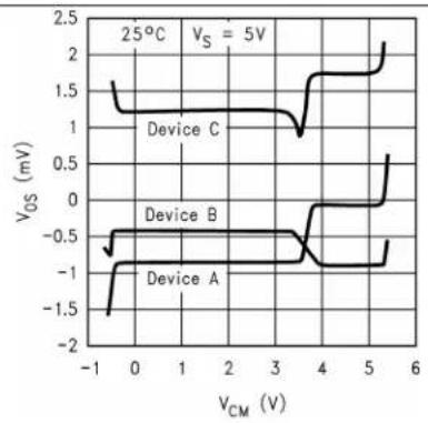
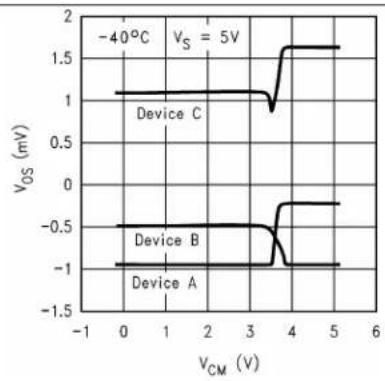
6.8TypicalCharacteristics
T_A=25^ , Unless Otherwise Noted
line
| V_CM (V) | V_OS (mV) - Device A | V_OS (mV) - Device B | V_OS (mV) - Device C | | -------- | -------------------- | -------------------- | -------------------- | | -1 | -1.5 | -0.5 | 1.5 | | 0 | -1.0 | -0.5 | 1.5 | | 1 | -1.0 | -0.5 | 1.5 | | 2 | -1.0 | -0.5 | 1.5 | | 3 | -1.0 | -0.5 | 1.5 | | 4 | -1.0 | 0.0 | 1.5 | | 5 | -1.0 | 0.0 | 1.5 | | 6 | -1.0 | 0.5 | 2.0 |Figure1.V OS vs.V CM for3RepresentativeUnitsFigure2.V
line
| V_CM (V) | V_OS (mV) | | -------- | --------- | | -40°C | 1.0 | | 3.5 | 0.8 | | 4.0 | 1.6 | | 5.0 | 1.6 |os vs.V CM for3RepresentativeUnits

line
| V_CM (V) | V_OS (mV) - Device A | V_OS (mV) - Device B | V_OS (mV) - Device C | | -------- | -------------------- | -------------------- | -------------------- | | -1 | -1.0 | -1.0 | 1.3 | | 0 | -1.0 | -0.5 | 1.3 | | 1 | -1.0 | -0.5 | 1.3 | | 2 | -1.0 | -0.5 | 1.3 | | 3 | -1.0 | -0.5 | 1.3 | | 4 | -1.0 | 0.0 | 1.5 | | 5 | -1.0 | 0.0 | 2.5 | | 6 | -1.0 | 0.0 | 2.5 |Figure3.V OS vs.V CM for3RepresentativeUnitsFigure4.V

line
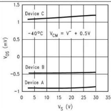
| Device | V_S (V) | V_OS (mV) | |--------|---------|-----------| | Device A | 30 | -0.8 | | Device B | 30 | -0.4 | | Device C | 30 | 1.4 |os vs. V s for3RepresentativeUnits
line
| Device | VOS (mV) | |--------|----------| | Device A | -0.9 | | Device B | -0.5 | | Device C | 1.2 |Figure5.V os vs. V s for3RepresentativeUnits

line
| Device | V_S (V) | V_OS (mV) | | -------- | ------- | --------- | | Device A | 30 | -0.9 | | Device B | 30 | -0.6 | | Device C | 30 | 1.4 |Figure6.V os vs. V s for3RepresentativeUnits
TypicalCharacteristics(continued)
T_A=25^ , Unless Otherwise Noted
line
| V_CM (V) | I_G (nA) | | -------- | -------- | | -1 | -1500 | | 0 | -1500 | | 1 | -1500 | | 2 | -1500 | | 3 | -1500 | | 4 | 500 | | 5 | 500 | | 6 | 500 |Figure7.1 B vs. V CM

line
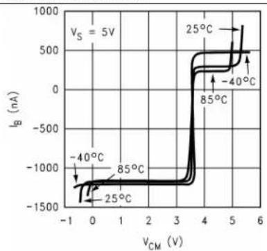
| v_S (V) | I_g (mA) at -40°C | I_g (mA) at 25°C | I_g (mA) at 85°C | | ------- | ----------------- | ---------------- | ---------------- | | 0 | -1280 | -1200 | -1150 | | 5 | -1250 | -1170 | -1120 | | 10 | -1220 | -1140 | -1090 | | 15 | -1190 | -1110 | -1060 | | 20 | -1160 | -1080 | -1030 | | 25 | -1130 | -1050 | -1000 | | 30 | -1100 | -1020 | -970 |Figure8.I B vs.V S
line
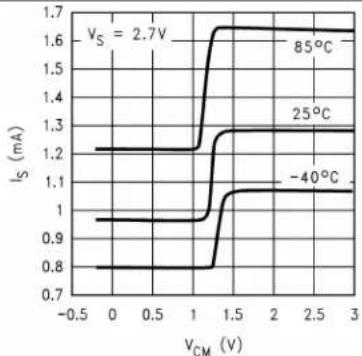
| V_CM (V) | I_S (mA) at -40°C | I_S (mA) at 25°C | I_S (mA) at 85°C | | -------- | ----------------- | ---------------- | ---------------- | | -0.5 | 0.8 | 0.9 | 1.2 | | 0 | 0.8 | 0.9 | 1.2 | | 1 | 0.8 | 0.9 | 1.2 | | 1.5 | 1.1 | 1.3 | 1.6 | | 2 | 1.1 | 1.3 | 1.6 | | 2.5 | 1.1 | 1.3 | 1.6 | | 3 | 1.1 | 1.3 | 1.6 |Figure9.1 S vs. V CM
line
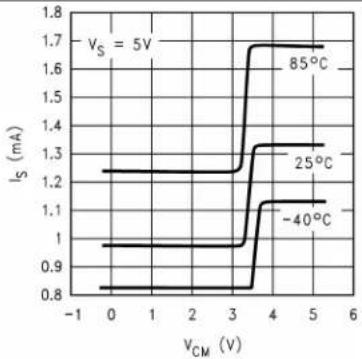
| V_CM (V) | I_S (mA) at -40°C | I_S (mA) at 25°C | I_S (mA) at 85°C | | -------- | ----------------- | ---------------- | ---------------- | | -1 | 0.8 | 1.0 | 1.2 | | 0 | 0.8 | 1.0 | 1.2 | | 3 | 0.8 | 1.0 | 1.2 | | 4 | 1.1 | 1.3 | 1.7 | | 5 | 1.1 | 1.3 | 1.7 | | 6 | 1.1 | 1.3 | 1.7 |Figure10.I s vs.V CM
line
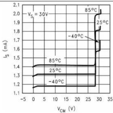
| V_CM (V) | I_S (mA) | | -------- | -------- | | -5 | 1.1 | | 0 | 1.2 | | 5 | 1.3 | | 10 | 1.4 | | 15 | 1.4 | | 20 | 1.4 | | 25 | 1.4 | | 30 | 1.6 | | 35 | 2.0 |Figure11. I s vs. V CM

line
| V_S (V) | -40°C | 25°C | 85°C | | ------- | ----- | ---- | ---- | | 0 | 0.78 | 0.92 | 1.18 | | 30 | 0.92 | 1.06 | 1.38 |Figure12. I S vs. V S (PNPside)
TypicalCharacteristics(continued)
T_A=25^ , Unless Otherwise Noted

line
| V_S (V) | 85°C (mA) | 25°C (mA) | -40°C (mA) | | ------- | --------- | --------- | ---------- | | 0 | 1.6 | 1.3 | 1.1 | | 30 | 2.1 | 1.5 | 1.3 |Figure13. I s vs. V s (NPNside)
line
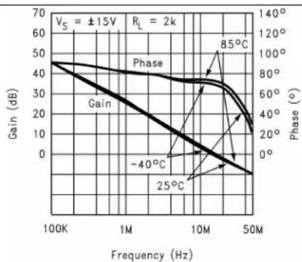
| Frequency (Hz) | Gain (dB) | Phase (°) | | -------------- | --------- | --------- | | 100K | 45 | 0 | | 1M | 30 | 20 | | 10M | 10 | 60 | | 50M | 0 | 0 |Figure14.Gain/Phasevs.Frequency

line
| Vs (V) | fU (MHz) at -40°C | fU (MHz) at +25°C | fU (MHz) at +85°C | | ------ | ----------------- | ----------------- | ----------------- | | 0 | 9.0 | 9.0 | 9.0 | | 5 | 10.5 | 11.0 | 11.5 | | 10 | 11.5 | 12.0 | 12.5 | | 15 | 12.5 | 13.0 | 13.5 | | 20 | 13.0 | 13.5 | 14.0 | | 25 | 13.5 | 14.0 | 14.5 | | 30 | 14.0 | 14.5 | 15.0 |Figure15. UnityGainFrequencyvs.V
line
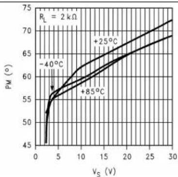
| V_S (V) | PM (°) at -40°C | PM (°) at +85°C | PM (°) at +25°C | | ------- | --------------- | --------------- | --------------- | | 0 | 45 | 45 | 45 | | 5 | 55 | 55 | 55 | | 10 | 60 | 60 | 60 | | 15 | 65 | 65 | 65 | | 20 | 70 | 70 | 70 | | 25 | 72 | 72 | 72 | | 30 | 73 | 73 | 73 |Figure16.PhaseMarginvs.V

line
| V_S (V) | f_U (MHz) | PM (°) | | ------- | --------- | ------ | | 0 | 10 | 40 | | 5 | 12 | 50 | | 10 | 13 | 60 | | 15 | 14 | 65 | | 20 | 14.5 | 68 | | 25 | 15 | 70 | | 30 | 15.5 | 70 |Figure17. UnityGainFreq.andPhaseMarginvs.V
line
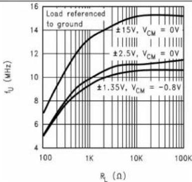
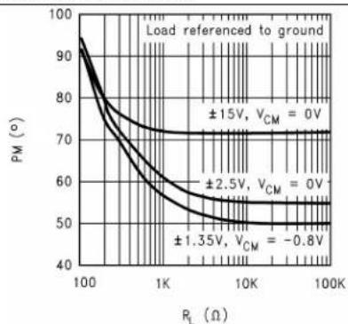
| R_L (Ω) | f_U (MHz) for ±15V, V_CM = 0V | f_U (MHz) for ±2.5V, V_CM = 0V | f_U (MHz) for ±1.35V, V_CM = -0.8V | | ------- | ----------------------------- | ------------------------------ | ---------------------------------- | | 100 | ~7 | ~6 | ~5 | | 1K | ~13 | ~10 | ~8 | | 10K | ~15 | ~11 | ~9 | | 100K | ~15 | ~11 | ~9 |Figure18. UnityGainFrequency vs. Load
TypicalCharacteristics(continued)
T_A=25^, Unless Otherwise Noted
line
| Load referenced to ground | PM (°) at ±15V, VCM = 0V | PM (°) at ±2.5V, VCM = 0V | PM (°) at ±1.35V, VCM = -0.8V | | -------------------------- | -------------------------- | -------------------------- | ------------------------------ | | 100 | 95 | 90 | 85 | | 1K | 70 | 65 | 60 | | 10K | 55 | 50 | 45 | | 100K | 50 | 45 | 40 |Figure19.PhaseMarginvs.Load
line
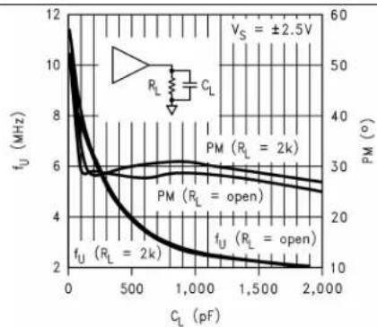
| CL (pF) | fU (MHz) - PM (RL = 2k) | fU (MHz) - PM (RL = open) | | ------- | ------------------------ | -------------------------- | | 0 | 12 | 6 | | 500 | 6 | 30 | | 1000 | 4 | 25 | | 1500 | 3 | 20 | | 2000 | 2 | 15 |Figure20. UnityGainFreq.andPhaseMarginvs.C
line
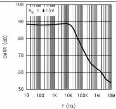
| f (Hz) | CMRR (dB) | | ------ | --------- | | 10 | 89 | | 100 | 89 | | 1K | 89 | | 10K | 89 | | 100K | 75 | | 1M | 60 | | 10M | 55 |
line
| f (Hz) | +PSRR (dB) for V_S = 2.7V | +PSRR (dB) for V_S = 5V | +PSRR (dB) for V_S = 30V | | ------ | -------------------------- | ------------------------ | ------------------------- | | 10 | ~90 | ~105 | ~110 | | 100 | ~85 | ~100 | ~105 | | 1K | ~75 | ~90 | ~95 | | 10K | ~60 | ~75 | ~80 | | 100K | ~40 | ~55 | ~60 | | 1M | ~20 | ~35 | ~40 |Figure21.CMRRvs.FrequencyFigure22.+PSRRvs.Frequency

line
| f (Hz) | -PSRR (dB) for V_S = 30V | -PSRR (dB) for V_S = 5V | -PSRR (dB) for V_S = 2.7V | | ------ | ------------------------ | ----------------------- | ------------------------- | | 10 | ~95 | ~90 | ~85 | | 100 | ~90 | ~85 | ~80 | | 1K | ~85 | ~80 | ~75 | | 10K | ~70 | ~65 | ~60 | | 100K | ~40 | ~35 | ~30 | | 1M | ~20 | ~15 | ~10 |Figure23.-PSRRvs.Frequency

line
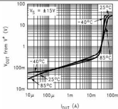
| I_OUT (A) | V_OUT from V* (V) | | --------- | ----------------- | | 10μ | ~10m | | 100μ | ~100m | | 1m | ~100m | | 10m | ~100m | | 100m | ~100m |Figure24. Output Voltage vs. Output Sourcing Current
TypicalCharacteristics(continued)
T_A=25^ , Unless Otherwise Noted
line
| IOUT (A) | VOUT from V+ (V) | | -------- | ---------------- | | 10μ | ~10m | | 100μ | ~100m | | 1m | ~100m | | 10m | ~100m | | 100m | ~100m |
line
| IOUT (A) | VOUT from V- (V) | | -------- | ---------------- | | 10μ | ~10m | | 100μ | ~100m | | 1m | ~100m | | 10m | ~100m | | 100m | ~100m |Figure25. OutputVoltagevs. OutputSourcingCurrentFigure26. OutputVoltagevs. OutputSinkingCurrent
line
| R_L (Ω) | V_OUT (V_PP) | | ------- | ------------ | | 10 | 1 | | 100 | 8 | | 1K | 9.5 | | 10K | 10 | | 100K | 10 |
line
| f (Hz) | VOUT(VPP) for RL = ±5V | VOUT(VPP) for RL = 2 kΩ | | ------ | ---------------------- | ----------------------- | | 10K | ~10 | ~10 | | 100K | ~10 | ~10 | | 1M | ~6 | ~6 | | 10M | ~0 | ~0 |Figure27.MaxOutputSwingvs.Load
line
| C_L (F) | % Overshoot | | ------- | ----------- | | 10p | 28 | | 100p | 62 | | 1000p | 60 | | 10n | 65 | | 100n | 63 | | 1μ | 40 | | 10μ | 0 |Figure28.MaxOutputSwingvs.Frequency
line
| C_L (F) | T_S (s) | | ------- | ------- | | 10p | 100n | | 100p | 100n | | 1000p | 1μ | | 10n | 1μ | | 100n | 1μ | | 1μ | 1μ | | 10μ | 10μ |Figure29.%Overshootvs.CapLoadFigure30.±5%SettlingTimevs.CapLoad
TypicalCharacteristics(continued)
T_A=25^, Unless Otherwise Noted
line
| C_L (F) | +SR (V/μs) at 85°C | +SR (V/μs) at 25°C | +SR (V/μs) at -40°C | | ------- | ------------------ | ------------------ | ------------------- | | 10p | ~20 | ~18 | ~14 | | 100p | ~20 | ~18 | ~14 | | 1000p | ~20 | ~18 | ~14 | | 10n | ~5 | ~3 | ~2 | | 100n | ~1 | ~1 | ~1 | | 1μ | ~0 | ~0 | ~0 |Figure31.+SRvs.CapLoad
line
| C_L (F) | -SR (V/μs) at 85°C | -SR (V/μs) at 25°C | -SR (V/μs) at -40°C | | ------- | ------------------ | ------------------ | ------------------- | | 10p | ~17 | ~12 | ~9 | | 100p | ~17 | ~12 | ~9 | | 1000p | ~16 | ~11 | ~8 | | 10n | ~10 | ~6 | ~4 | | 100n | ~3 | ~2 | ~1 | | 1μ | ~0 | ~0 | ~0 |Figure32.-SRvs.CapLoad
line
| C_L (F) | +Slew Rate (V/μs) for V_S = ±15V | +Slew Rate (V/μs) for V_S = ±1.35V | | ------- | -------------------------------- | ---------------------------------- | | 10p | ~10 | ~10 | | 100p | ~10 | ~10 | | 1000p | ~10 | ~10 | | 10n | ~1 | ~1 | | 100n | ~0.1 | ~0.1 | | 1μ | ~0.01 | ~0.01 | | 10μ | ~0.001 | ~0.001 |Figure33.+SRvs.CapLoadFigure34.-SRvs.CapLoad
line
| C_L (F) | -Slew Rate (V/μs) for V_S = ±1.35V | -Slew Rate (V/μs) for V_S = ±15V | | ------- | ---------------------------------- | -------------------------------- | | 10p | ~10 | ~10 | | 100p | ~10 | ~10 | | 1000p | ~10 | ~10 | | 10n | ~1 | ~1 | | 100n | ~0.1 | ~0.1 | | 1μ | ~0.01 | ~0.01 | | 10μ | ~0.001 | ~0.001 |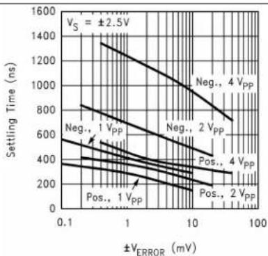
line
| ±V_ERROR (mV) | Settling Time (ns) for Neg., 1 V_PP | Settling Time (ns) for Neg., 2 V_PP | Settling Time (ns) for Pos., 1 V_PP | Settling Time (ns) for Pos., 2 V_PP | | ------------- | ----------------------------------- | ----------------------------------- | ----------------------------------- | ----------------------------------- | | 0.1 | ~600 | ~800 | ~400 | ~500 | | 1 | ~500 | ~700 | ~350 | ~450 | | 10 | ~350 | ~500 | ~250 | ~350 | | 100 | ~250 | ~350 | ~200 | ~300 |Figure35.SettlingTimevs.ErrorVoltage

line
| ±V_ERROR (mV) | Settling Time (ns) for Neg., 1 V_PP | Settling Time (ns) for Pos., 5 V_PP | Settling Time (ns) for Neg., 2 V_PP | Settling Time (ns) for Pos., 1 V_PP | Settling Time (ns) for Pos., 2 V_PP | | ------------- | ----------------------------------- | ----------------------------------- | ----------------------------------- | ----------------------------------- | ----------------------------------- | | 0.1 | 600 | 400 | 300 | 200 | 100 | | 1 | 500 | 350 | 250 | 150 | 80 | | 10 | 400 | 300 | 200 | 100 | 60 | | 100 | 300 | 250 | 150 | 50 | 40 |Figure36.SettlingTimevs.ErrorVoltage
TypicalCharacteristics(continued)
T_A=25^ , Unless Otherwise Noted
line
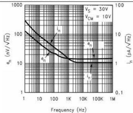
| Frequency (Hz) | e_n (nV/√Hz) | i_n (pA/√Hz) | | -------------- | ------------ | ------------ | | 1 | ~200 | ~10 | | 10 | ~100 | ~5 | | 100 | ~30 | ~2 | | 1K | ~10 | ~1 | | 10K | ~5 | ~1 | | 100K | ~2 | ~1 | | 1M | ~1 | ~1 |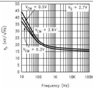
line
| Frequency (Hz) | e_n (nV/√Hz) for V_CM = 0.2V | e_n (nV/√Hz) for V_CM = 0.5V | e_n (nV/√Hz) for V_CM = 2.6V | | -------------- | ----------------------------- | ----------------------------- | ----------------------------- | | 10 | ~45 | ~45 | ~45 | | 100 | ~25 | ~30 | ~35 | | 1K | ~18 | ~20 | ~22 | | 10K | ~16 | ~17 | ~18 | | 100K | ~15 | ~16 | ~17 |CM
Figure37.InputNoiseVoltage/Currentvs.FrequencyFigure38.InputNoiseVoltageforVariousV

line
| Frequency (Hz) | in (pA/√Hz) for VCM = 0.5V | in (pA/√Hz) for VCM = 0.2V | in (pA/√Hz) for VCM = 2.6V | | -------------- | -------------------------- | -------------------------- | -------------------------- | | 10 | ~4.5 | ~3.5 | ~1.5 | | 100 | ~2.5 | ~2.0 | ~0.8 | | 1K | ~1.5 | ~1.2 | ~0.5 | | 10K | ~0.8 | ~0.6 | ~0.3 | | 100K | ~0.5 | ~0.4 | ~0.2 |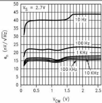
line
| v_CM (V) | e_n (nV/√Hz) at 10 Hz | e_n (nV/√Hz) at 100 Hz | e_n (nV/√Hz) at 1 KHz | e_n (nV/√Hz) at 10 KHz | | -------- | --------------------- | ---------------------- | --------------------- | ---------------------- | | 0.0 | ~30 | ~20 | ~15 | ~10 | | 0.5 | ~40 | ~22 | ~16 | ~11 | | 1.0 | ~40 | ~22 | ~16 | ~11 | | 1.5 | ~40 | ~22 | ~16 | ~11 | | 2.0 | ~45 | ~22 | ~16 | ~11 | | 2.5 | ~45 | ~22 | ~16 | ~11 |Figure40.InputNoiseVoltagevs.V CM
Figure39.InputNoiseCurrentforVariousV CM
line
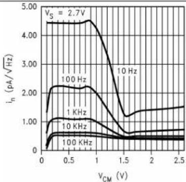
| V_CM (V) | 100 Hz | 1 KHz | 10 KHz | 100 KHz | | -------- | ------ | ----- | ------ | ------- | | 0.0 | 4.5 | 2.2 | 1.0 | 0.5 | | 0.5 | 4.5 | 2.2 | 1.0 | 0.5 | | 1.0 | 4.5 | 2.2 | 1.0 | 0.5 | | 1.5 | 1.2 | 1.3 | 0.6 | 0.5 | | 2.0 | 1.3 | 1.4 | 0.6 | 0.5 | | 2.5 | 1.4 | 1.5 | 0.6 | 0.5 |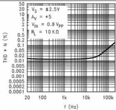
line
| f (Hz) | THD + N (%) | | ------ | ----------- | | 20 | 0.01 | | 100 | 0.01 | | 1k | 0.01 | | 10k | 0.01 | | 100k | 0.2 |Figure41.InputNoiseCurrentvs.V CM
Figure42.THD+Nvs.Frequency
TypicalCharacteristics(continued)
T_A=25^, Unless Otherwise Noted

line
| f (Hz) | THD + N (%) | | ------ | ----------- | | 20 | 0.01 | | 100 | 0.01 | | 1k | 0.01 | | 10k | 0.01 | | 100k | 0.05 |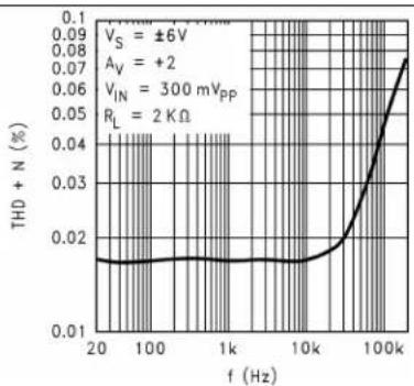
line
| f (Hz) | THD + N (%) | | ------ | ----------- | | 20 | 0.015 | | 100 | 0.015 | | 1k | 0.015 | | 10k | 0.015 | | 100k | 0.07 |Figure43.THD+Nvs.FrequencyFigure44.THD+Nvs.Frequency

line
| V_INPP (V) | THD + N (%) | | ---------- | ----------- | | 1m | 5.0 | | 10m | 1.0 | | 100m | 0.02 | | 1 | 0.03 | | 6 | 0.04 |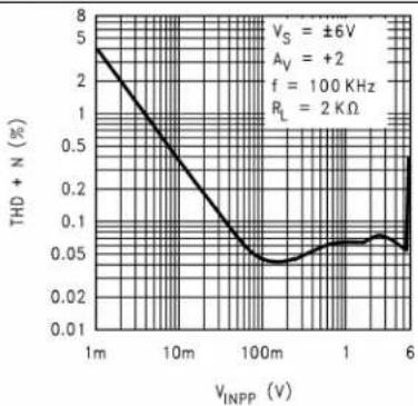
line
| V_INPP (V) | THD + N (%) | | ---------- | ----------- | | 1m | 5.0 | | 10m | 1.0 | | 100m | 0.05 | | 1 | 0.07 | | 6 | 0.05 |Figure45.THD+Nvs.AmplitudeFigure46.THD+Nvs.Amplitude
line
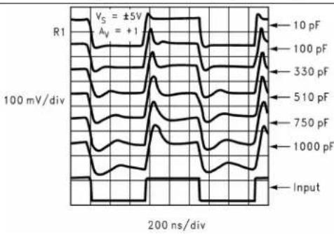
| Voltage (pF) | Time (ns) | | ------------ | --------- | | 10 | 0 | | 100 | 0 | | 330 | 0 | | 510 | 0 | | 750 | 0 | | 1000 | 0 | | Input | 0 |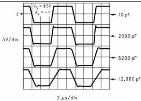
line
| Voltage Level | Time Scale (μs) | | ------------- | --------------- | | 10 pF | 2 | | 2000 pF | 2 | | 8200 pF | 2 | | 12,900 pF | 2 |Figure47.SmallSignalStepResponse
Figure48.LargeSignalStepResponse
7ApplicationandImplementation
7.1 Block Diagram and Operational Description
7.1.1A) InputStage
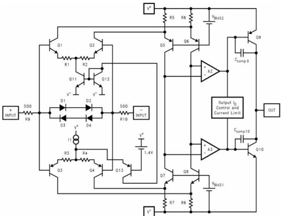
text_image
V+ R5 R6 VBIAS2 Q9 Ccomp 9 Q1 Q2 R1 R2 Q11 Q12 V- V- + INPUT S00 R9 D1 D2 500 - INPUT D3 D4 I1 R3 R4 Q3 Q4 Q13 V* V* 1.4V Output I0 Control and Current Limit Ccomp10 Q10 V-BIAS1 R7 R8 V-Figure49.SimplifiedSchematicDiagram
As seen in Figure 49, the input stage consists of two distinct differential pairs (Q1-Q2 and Q3-Q4) in order to accommodate the full Rail-to-Rail input common mode voltage range. The voltaged drop across R5, R6, R7, and R8 is kept to less than 200 m Vin order to allow the input to exceed the supply rails. Q13 acts as a switch to steercurrent away from Q3-Q4 and into Q1-Q2, asthe input increases beyond 1.4 V of V ^+ . This turnshifts the signal path from the bottom staged differential pair to the top one and causes a subsequent increase in the supply current.
Intransitioningfromonestagetoanother,certaininputstageparameters(V basedonwhichdifferentialpairis"on"atthetime.InputBiascurrent,I B,willchangeinvalueandpolarityasthe inputcrossesthetransitionregion.Inaddition,parameterssuchasPSRRandCMRRwhichinvolvetheinput offsetvoltagewillalsobeeffectedbychangesinV CM acrossthedifferentialpairtransitionregion.
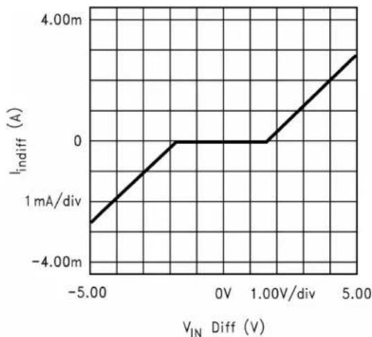
TheinputstageisprotectedwiththecombinationofR9-R10andD1,D2,D3,andD4againstdifferentialinput over-voltages. Thisfaultconditioncouldotherwiseharmthedifferentialpairsorcauseoffsetvoltageshiftincase of prolonged over voltage. As shown in Figure 50, if this voltage reaches approximately ±1.4 V at 25°C, the diodesturnonandcurrentflowislimitedbytheinternalseriesresistors(R9andR10).TheAbsoluteMaximum Ratingof±10VdifferentialonV _IN stillneedstobeobserved.Withtemperaturevariation,thepointwerethe diodesturnonwillchangeattherateof5mV/°C.
BlockDiagramandOperationalDescription(continued)
line
| VIN Diff (V) | I_indiff (A) | | ------------ | ------------ | | -5.00 | -4.00m | | 0 | 0 | | 1.00 | 0 | | 5.00 | 4.00m |Figure50.InputStageCurrentvs.DifferentialInputVoltage
7.1.2B)OutputStage
The output stage Figure 49 is comprised of complementary NPN and PNP common-emitter stages to permit voltageswingtowithinaV CE(SAT) ofeithersupplyrail.Q9suppliesthesourcingandQ10suppliesthesinking currentload.OutputcurrentlimitingisachievedbylimitingtheV CE ofQ9andQ10;usingthisapproachtocurrent limiting, alleviatesthedrawbacktotheconventionalschemewhichrequiresoneV BE reductioninoutputswing.
The frequency compensation circuit includes Millercapacitors from collectortobase of each output transistor (see Figure 49, C comp9 and C comp10). At light capacitiveloads, the high frequency gain of the output transistors is high, and the Miller effect increases the effective value of the capacitor there by stabilizing the Op Amp. Large capacitiveloads greatly decrease the high frequency gain of the output transistor thus lowering the effective internal Miller capacitance - the internal pole frequency increases at the same time a low frequency pole is created at the Op Amp output dueto the large load capacitor. In this fashion, the internal dominant pole compensation, which works by reducing the loop gaintoles than 0 dB when the phases shift around the feedback loopism more than 180^ , varies with the amount of capacitive load and becomes less dominant when the load capacitor has increased enough. Hence the Op Amp is very stable even at high values of load capacitance resulting in the uncharacteristic feature of stability under all capacitive loads.
7.2DrivingCapacitiveLoads
The LM8261 is specifically designed to drive unlimited capacitive loads without oscillations (See Figure 30). In addition, the output current handling capability of the device allows for goods slewing characteristics even with large capacitive loads (see Slew Rate vs. Cap Load plots, Figure 31 through Figure 34). The combination of these features is ideal for application such as TFT flat panel buffers, A/D converter input amplifiers, and so forth.
However, as in most Op Amps, addition of a series isolation resistor between the Op Amp and the capacitive load improves settling and overshoot performance.
Outputcurrentdriveisanimportantparameterwhendrivingcapacitiveloads. This parameter will determine how fast the output voltage can change. Referring to the Slew Rate vs. Cap Load Plots (Figure 31 through Figure 34), twodistinctregionscanbeidentified.Belowabout10,000pF,theoutputSlewRateissolelydeterminedbythe OpAmp'scompensationcapacitorvalueandavailablecurrentintothatcapacitor.Beyond10nF,theSlewRateis determinedbytheOpAmp'savailableoutputcurrent.Notethatbecauseoftheloweroutputsourcingcurrent comparedtothesinkingone,theSlewRatelimitunderheavycapacitiveloadingisdeterminedbythepositive transitions.Anestimateofpositiveandnegativeslewratesforloadslargerthan100nFcanbemadebydividing theshortcircuitcurrentvaluebythecapacitor.
DrivingCapacitiveLoads(continued)
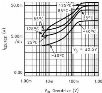
For the LM8261, the available output current increases with the input overdrive. As seen in Figure 51 and Figure 52, both sourcing and sinking short circuit current increase as input overdrive increases. In a closed loop amplifier configuration, during transient conditions while the feedback output has not quite caught up with the input, there will be an overdrive imposed on the input allowing more output current than would normally be available under steady state condition. Because of this feature, the OpAmp's output stage quiescent current can be kept to a minimum, thereby reducing power consumption, while enabling the device to deliver large output current when the needarises (such as during transients).
line
| V_IN Overdrive (V) | I_SOURCE (A) | | ------------------ | ----------- | | 1.00m | 0.00 | | 10m | 5.00m /div | | 100m | 50.0m | | 1.00m | 50.0m |Figure51.OutputShortCircuitSourcingCurrentvs.InputOverdrive

line
| V_IN Overdrive (V) | I_SINK (A) at 25°C | I_SINK (A) at 125°C | I_SINK (A) at 85°C | I_SINK (A) at 25°C | I_SINK (A) at -40°C | | ------------------ | ----------------- | ------------------ | ----------------- | ----------------- | ------------------ | | 1.00m | ~0.00 | ~0.00 | ~0.00 | ~0.00 | ~0.00 | | 10m | ~1.0m | ~1.0m | ~1.0m | ~1.0m | ~1.0m | | 0.1 | ~10.0m | ~10.0m | ~10.0m | ~10.0m | ~10.0m | | 1 | ~100.0m | ~100.0m | ~100.0m | ~100.0m | ~100.0m |Figure52.OutputShortCircuitSinkingCurrentvs.InputOverdrive
DrivingCapacitiveLoads(continued)
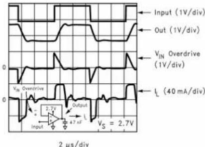
Figure 53 shows the output voltage, output current, and the resulting input overdrive with the device set for A_V = +1 and the input tied to a 1V step function driving a 47nF capacitor. During the output transition, the input overdrive reaches 1V peak and is more than one ought to cause the output current to increase its maximum value (see Figure 51 and Figure 52). Because the larger output sinking current is compared to the sourcing one, the output negativetransition is faster than the positive one.
line
| Signal | Value | |-----------------|-----------| | Input | 2.7V | | Output | 40 mA/div | | V_IN Overdrive | 1V/div | | I_L | 40 mA/div | | V_S | 2.7V |Figure53.BufferAmplifierScopePhoto
7.3 Estimating the Output Voltage Swing
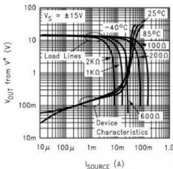
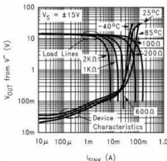
It is important to keep in mind that the steady state output current will be less than the current available when there is an input overdrive present. For steady state conditions, Figure 24 through Figure 26 in Typical Characteristics can be used to predict the output swing. Figure 54 and Figure 55 show this performance along with several load lines corresponding to load stied between the output and ground. In each cases, the intersection of the device plot at the appropriate temperature with the load line would be the typical output swing possible for that load. For example, a 1-KΩ load can accommodate an output swing to within 250 mV of V⁻ and to 330mV of V⁺ (VS = ±15V) corresponding to atypical 29.3V PP unclipped swing.
line
| I_SOURCE (A) | V_OUT from V* (V) | |-------------|-------------------| | 10μ | ~10m | | 100μ | ~10m | | 1m | ~10m | | 10m | ~10m | | 100m | ~10m | | 1.0 | ~10m |Figure54.OutputSourcingCharacteristicswithLoadLines
line
| I_SINK (A) | V_OUT from V (V) | | ---------- | ---------------- | | 10μ | ~10m | | 100μ | ~10m | | 1m | ~10m | | 10m | ~10m | | 100m | ~10m | | 1.0 | ~10m |Figure55.OutputSinkingCharacteristicswithLoadLines
7.4TFTApplications
Figure 56 below, shows a typical application where the LM8261 is used as a buffer amplifier for the V_COM signal employedinaTFTLCDflatpanel:
text_image
+5V VREF - -5V IL VOUT 10 10 10 0.05μ 0.05μ 0.05μ 0.05μ Simulated TFT Load Column Driver OutputsFigure56.V COM DriverApplicationSchematic
Figure57showsthetimedomainresponseoftheamplifierwhenusedasaV COM buffer/driverwithV REF at ground.Inthisapplication,theOpAmploopwilltryandmaintainitsoutputvoltagebasedonthevoltageonits non-invertinginput(V _REF )despitethecurrentinjectedintotheTFTsimulatedload.Aslongasthisloadcurrentis withintherangetolerablebytheLM8261(45mAsourcingand65mAsinkingfor±5Vsupplies),theoutputwill settletoitsfinalvaluewithinlessthan2μs.

line
| Time (μs) | Voltage (V) | |-----------|-------------| | 0 | 0 | | 1 | 0 | | 2 | 0 | | 3 | 0 | | 4 | 0 | | 5 | 0 | | 6 | 0 | | 7 | 0 | | 8 | 0 | | 9 | 0 | | 10 | 0 | | 11 | 0 | | 12 | 0 | | 13 | 0 | | 14 | 0 | | 15 | 0 | | 16 | 0 | | 17 | 0 | | 18 | 0 | | 19 | 0 | | 20 | 0 | | 21 | 0 | | 22 | 0 | | 23 | 0 | | 24 | 0 | | 25 | 0 | | 26 | 0 | | 27 | 0 | | 28 | 0 | | 29 | 0 | | 30 | 0 | | 31 | 0 | | 32 | 0 | | 33 | 0 | | 34 | 0 | | 35 | 0 | | 36 | 0 | | 37 | 0 | | 38 | 0 | | 39 | 0 | | 40 | 0 | | 41 | 0 | | 42 | 0 | | 43 | 0 | | 44 | 0 | | 45 | 0 | | 46 | 0 | | 47 | 0 | | 48 | 0 | | 49 | 0 | | 50 | 0 | | 51 | 0 | | 52 | 0 | | 53 | 0 | | 54 | 0 | | 55 | 0 | | 56 | 0 | | 57 | 0 | | 58 | 0 | | 59 | 0 | | 60 | 0 | | 61 | 0 | | 62 | 0 | | 63 | 0 | | 64 | 0 | | 65 | 0 | | 66 | 0 | | 67 | 0 | | 68 | 0 | | 69 | 0 | | 70 | 0 | | 71 | 0 | | 72 | 0 | | 73 | 0 | | 74 | 0 | | 75 | 0 | | 76 | 0 | | 77 | 0 | | 78 | 0 | | 79 | 0 | | 80 | 0 | | 81 | 0 | | 82 | 0 | | 83 | 0 | | 84 | 0 | | 85 | 0 | | 86 | 0 | | 87 | 0 | | 88 | 0 | | 89 | 0 | | 90 | 0 | | 91 | 0 | | 92 | 0 | | 93 | 0 | | 94 | 0 | | 95 | 0 | | 96 | 0 | | 97 | 0 | | 98 | 0 | | 99 | 0 | | Note: The actual values in the CSV data are not provided in the code. The code contains repeated 'V' and 'I' markers for the second wave signal.Figure57.V COM DriverPerformanceScopePhoto
7.5 Output Short Circuit Current and Dissipation Issues
TheLM8261outputstageisdesignedformaximumoutputcurrentcapability. Even though momentary output shortstogroundandeithersupplycanbetoleratedatalloperatingvoltages, longer lastingshortconditions can cause the junction temperature or rise beyond the absolute maximum rating of the device, especially at higher supply voltage conditions. Below supply voltage of 6V, output short circuit condition can be tolerated indefinitely.
WiththeOpAmptiedtoaload, thedevicepowerdissipationconsistsofthequiescentpowerduetothesupply currentflowintothedevice,inadditiontopowerdissipationduetotheloadcurrent.Theloadportionofthe poweritselfcouldincludeanaveragevalue(duetoaDCloadcurrent)andanACcomponent.DCloadcurrent wouldflowifthereisanoutputvoltageoffset,ortheoutputACaveragecurrentisnon-zero,oriftheOpAmp operatesinasinglesupplyapplicationwheretheoutputismaintainedsomewhereintherangeoflinear operation.Therefore:
$$ P _ {\text { TOTAL }} = P _ {Q} + P _ {D C} + P _ {A C} \tag {1} $$
OpAmpQuiescentPowerDissipation:
$$ P _ {Q} = I _ {S} \cdot V _ {S} \tag {2} $$
DCLoadPower:
$$ P _ {D C} = I _ {O} \cdot (V _ {R} - V _ {O}) (3) $$
ACLoadPower:
$$ P _ {A C} = (\text { outlined intable below }) $$
OutputShortCircuitCurrentandDissipationIssues(continued)
where
- I_S isSupplyCurrent
• V_S is TotalSupplyVoltage(V + - V-)
• I_0 isAverageLoadCurrent
• V_o isAverageOutputVoltage - V_R is V^+ for sourcing and V^- for sinking current(4)
Table 1 show sthemaximum AC component of the load power dissipated by the Op Amp for standard Sinusoidal, Triangular, and Square Waveforms:
Table1.NormalizedACPowerDissipatedintheOutputStageforStandardWaveforms
| P_AC (W. /V2) | ||
| SinusoidalTriangularSquare | ||
| 50.7x10⁻³ | 46.9x10⁻³ | 62.5x10⁻³ |
ThetableentriesarenormalizedtoV S^2/RL . TocalcatetheACloadcurrentcomponentofpowerdissipation, simplymultiplythetableentrycorrespondingtotheoutputwaveformbythefactorV S^2/RL . Forexample, with±15 V supplies, a 600-Ω load, and triangular waveform power dissipation in the output stage is calculated as:
$$ P _ {A C} = (4 6. 9 \times 1 0 ^ {- 3}) \cdot [ 3 0 ^ {2} / 6 0 0 ] = 7 0. 4 \mathrm{mW} (5) $$
7.6 Other Application Hints
Theuseofsupplydecouplingismandatoryinmostapplications.Aswithmostrelativelyhighspeed/highoutput currentOpAmps,bestresultsareachievedwheneachsupplylineisdecoupledwithtwocapacitors;asmall value ceramic capacitor ( 0.01 F ) placed very close to the supply lead in addition to a large value Tantalum or Aluminum ( >4.7 F ). The large capacitor can be shared by more than one device if necessary. The small ceramiccapacitormaintainslowsupplyimpedanceathighfrequencieswhilethelargecapacitorwillactasthe charge "bucket" for fast load current spikes at the Op Amp output. The combination of these capacitors will providesupplydecouplingandwillhelpkeeptheOpAmposcillationfreeunderanyload.
7.6.1 LM8261Advantages
ComparedtootherRail-to-RailInput/Outputdevices,theLM8261offersseveraladvantagessuchas:
- Improvedcrossoverdistortion.
- Nearlyconstantsupplycurrentthroughouttheoutputvoltageswingrangeandclosetoeitherrail.
- Consistentstabilityperformanceforallinput/outputvoltageandcurrentconditions.
- Nearly constant Unity gain frequency ( f_u ) and Phase Margin ( Phi_m ) for all operating supplies and load conditions.
- Nooutputphasereversalunderinputoverloadcondition.
8PowerSupplyRecommendations
TheLM8261canoperateoffasinglesupplyorwithdualsupplies. TheinputCMcapabilityoftheparts(CMVR) extendscoverstheentiresupplyvoltagerangeformaximumflexibility. Suppliesshouldbedecoupledwithlow inductance, oftenceramic, capacitorstogroundlessthan0.5inchesfromthedevicepins. Theuseofground planeisrecommended, andasinmosthighspeeddevices, itisadvisabletoremovegroundplanecloseto devicesensitivepinssuchastheinputs.
9Layout
9.1 LayoutGuidelines
Generally, agoodhighfrequencylayoutwillkeeppowersupplyandgroundtracesawayfromtheinvertinginput and outputpins.Parasiticcapacitancesonthesenodestogroundwillcausefrequencyresponsepeakingand possiblecircuitoscillations.TexasInstrumentssuggeststhefollowingevaluationboardsasaguideforhigh frequency layout and as an aid in device testing and characterization. See Table 2 for details. The LM8261 evaluationboard(s)isagoodexampleofhighfrequencylayouttechniquesasareference.Generalhigh-speed, signal-pathlayoutsuggestionsinclude:
- Continuousgroundplanesarepreferredforsignalroutingwithmatchedimpedancetracesforlongerruns. However,openupbothgroundandpowerplanesaroundthecapacitivesensitiveinputandoutputdevice pins as shown in Figure 58. After the signal is sent into a resistor, parasitic capacitance becomes more of a bandlimitingissueandlessofastabilityissue.
- Use good, high-frequency decoupling capacitors (0.1 μF) on the ground plane at the device power pins as shown in Figure 58. Higher value capacitors (2.2 μF) are required, but may be placed further from the device powerpinsandsharedamongdevices.Forbesthigh-frequencydecoupling,considerX2Ysupply-decoupling capacitorsthatofferamuchhigherself-resonancefrequencyoverstandardcapacitors.
- When using differentialsignal routing over any appreciable distance, use microstri layout techniques with matched impedancetraces.
- The input summing junction is very sensitivetoparasitic capacitance. ConnectanyRf, and Rgelements into the summing junction with minimal trace length to the device pin side of the resistor, as shown in Figure 59. The otherside of these element scan havemoretracelength if needed to the source ortoground.
9.2LayoutExample
text_image
Decoupling caps (C1, and C2) placed as close as possible to device power supply pins Continuous ground plane (except under components and sensitive nodes) VCC GND VEE J5 POWER C3 C5 TP3 J2 +IN RINb Ro OUT TP2 RTn U1 C1 TP1 DIS RTdis - IN DIS J4Figure58.LM8261EvaluationBoardLayer1
text_image
VEE GND VCC POWER U5 RGND J2 J3 C4 RF +IN RGa OUT DIS J1 UL94V-0 GND MADE IN U.S. -IN 551600542-001REV A 980600542- DIS J4 RF and RGa placed on board bottom to minimize summing junction parasitics by reducing trace length EVM Board Layout ExampleFigure59.LM8261EvaluationBoardLayer2
Table2.EvaluationBoardComparison
| DEVICEPACKAGEEVALUATIONBOARDPARTNUMBER | |
| LM8261M5SOT-23LMH730216 | |
10DeviceandDocumentationSupport
10.1 DocumentationSupport
10.1.1 RelatedDocumentation
For related documentation, see IC Package Thermal Metrics Application Report, SPRA953
10.2Trademarks
Alltrademarksarethepropertyoftheirrespectiveowners.
10.3 Electrostatic Discharge Caution

These devices have limited built-in ESD protection. The leads should be shorted together or the device placed in conductive foam duringstorageorhandlingtopreventelectrostaticdamagetotheMOSgates.
10.4 Glossary
SLYZ022—TIGlossary.
This glossarylistsandexplainsterms,acronyms,anddefinitions.
11 Mechanical, Packaging, and Orderable Information
The following pages include mechanical, packaging, and orderable information. This information is the most current data available for the designated devices. This data subject to changewithout notice and revision of this document. For browser-based version of this datasheet, referto the left-hand navigation.
PACKAGING INFORMATION
| Orderable Device Status(1) | Package Type Package Drawing | Pins Package Qty | Eco Plan(2) | Lead finish/ Ball material(6) | MSL Peak Temp(3) | Op Temp (°C) | Device Marking(4/5) | Samples |
| LM8261M5 NRND SOT-23 DBV 5 1000 Non-RoHS | Call TI Level-1-260C-UNLIM -40 to 85 A45A | |||||||
| LM8261M5/NOPB ACTIVE SOT-23 DBV 5 1000 RoHS & Green SN Level-1-260C-UNLIM -40 to 85 A45A | Samples | |||||||
| LM8261M5X | NRND SOT-23 DBV 5 3000 Non-RoHS | Call TI Level-1-260C-UNLIM -40 to 85 A45A | ||||||
| LM8261M5X/NOPB | ACTIVE SOT-23 DBV 5 3000 RoHS & Green SN Level-1-260C-UNLIM -40 to 85 A45A | Samples | ||||||
(1) The marketing status values are defined as follows:
ACTIVE: Product device recommended for new designs.
LIFEBUY: TI has announced that the device will be discontinued, and a lifetime-buy period is in effect.
NRND: Not recommended for new designs. Device is in production to support existing customers, but TI does not recommend using this part in a new design.
PREVIEW: Device has been announced but is not in production. Samples may or may not be available.
OBSOLETE: TI has discontinued the production of the device.
(2) RoHS: TI defines "RoHS" to mean semiconductor products that are compliant with the current EU RoHS requirements for all 10 RoHS substances, including the requirement that RoHS substance do not exceed 0.1% by weight in homogeneous materials. Where designed to be soldered at high temperatures, "RoHS" products are suitable for use in specified lead-free processes. TI may reference these types of products as "Pb-Free".
RoHS Exempt: TI defines "RoHS Exempt" to mean products that contain lead but are compliant with EU RoHS pursuant to a specific EU RoHS exemption.
Green: TI defines "Green" to mean the content of Chlorine (Cl) and Bromine (Br) based flame retardants meet JS709B low halogen requirements of <=1000ppm threshold. Antimony trioxide based flame retardants must also meet the <=1000ppm threshold requirement.
(3) MSL, Peak Temp. - The Moisture Sensitivity Level rating according to the JEDEC industry standard classifications, and peak solder temperature.
(4) There may be additional marking, which relates to the logo, the lot trace code information, or the environmental category on the device.
(5) Multiple Device Markings will be inside parentheses. Only one Device Marking contained in parentheses and separated by a "-" will appear on a device. If a line is indented then it is a continuation of the previous line and the two combined represent the entire Device Marking for that device.
(6) Lead finish/Ball material - Orderable Devices may have multiple material finish options. Finish options are separated by a vertical ruled line. Lead finish/Ball material values may wrap to two lines if the finish value exceeds the maximum column width.
Important Information and Disclaimer: The information provided on this page represents TI's knowledge and belief as of the date that it is provided. TI bases its knowledge and belief on information provided by third parties, and makes no representation or warranty as to the accuracy of such information. Efforts are underway to better integrate information from third parties. TI has taken and
continues to take reasonable steps to provide representative and accurate information but may not have conducted destructive testing or chemical analysis on incoming materials and chemicals. TI and TI suppliers consider certain information to be proprietary, and thus CAS numbers and other limited information may not be available for release.
In no event shall TI's liability arising out of such information exceed the total purchase price of the TI part(s) at issue in this document sold by TI to Customer on an annual basis.
TAPE AND REEL INFORMATION
*All dimensions are nominal
| Device Package | Type | Package Drawing | Pins | SPQ Reel | Diameter (mm) | Reel Width W1 (mm) | A0 (mm) | B0 (mm) | K0 (mm) | P1 (mm) | W (mm) | Pin1 Quadrant |
| LM8261M5 SOT-23 | DBV 5 10 | 000 178.0 | 8.4 3.2 | 3.2 1.4 4.0 | 8.0 Q3 | |||||||
| LM8261M5/NOPB SOT-23 | DBV | 5 1000 178.0 | 8.4 3.2 | 3.2 3.2 1.4 | 4.0 8.0 Q3 | |||||||
| LM8261M5X SOT-23 | DBV 5 30 | 000 178.0 | 8.4 3.2 | 3.2 1.4 4.0 | 8.0 Q3 | |||||||
| LM8261M5X/NOPB SOT-23 | DBV | 5 3000 178.0 | 8.4 3.2 | 3.2 3.2 1.4 | 4.0 8.0 Q3 |
text_image
TAPE AND REEL BOX DIMENSIONS W L*All dimensions are nominal
| Device | Package Type | Package Drawing | Pins | SPQ | Length (mm) | Width (mm) | Height (mm) |
| LM8261M5 SOT-23 | DBV 5 1000 208.0 | 191.0 35.0 | |||||
| LM8261M5/NOPB SOT-23 | DBV 5 1000 208.0 | 191.0 35.0 | |||||
| LM8261M5X SOT-23 | DBV 5 3000 208.0 | 191.0 35.0 | |||||
| LM8261M5X/NOPB SOT-23 | DBV 5 3000 208.0 | 191.0 35.0 |
SMALL OUTLINE TRANSISTOR
text_image
PIN 1 INDEX AREA 2X 0.95 1.9 5X 0.5 0.3 3 1.75 1.45 B 5 1.9 4 3.05 2.75 A 0.2 A B
text_image
C 0.1 C 1.45 0.90 (1.1) 0.15 TYP 0.00
text_image
0.25 GAGE PLANE 8° 0° TYP 0.6 TYP 0.3 SEATING PLANE 0.22 0.08 TYP4214839/F 06/2021
NOTES:
- All linear dimensions are in millimeters. Any dimensions in parenthesis are for reference only. Dimensioning and tolerancing per ASME Y14.5M.
- This drawing is subject to change without notice.
- Reference JEDEC MO-178.
- Body dimensions do not include mold flash, protrusions, or gate burrs. Mold flash, protrusions, or gate burrs shall not exceed 0.25 mm per side.
SMALL OUTLINE TRANSISTOR

text_image
5X (1.1) PKG 1 5X (0.6) 2 2X (0.95) 3 (R0.05) TYP (2.6) 4 SYMM (1.9)LAND PATTERN EXAMPLE
EXPOSED METAL SHOWN
SCALE:15X

text_image
SOLDER MASK OPENING METAL EXPOSED METAL 0.07 MAX ARROUNDNON SOLDER MASK
DEFINED
(PREFERRED)

text_image
METAL UNDER SOLDER MASK SOLDER MASK OPENING EXPOSED METAL 0.07 MIN ARROUNDSOLDER MASK
DEFINED
SOLDER MASK DETAILS
4214839/F 06/2021
NOTES: (continued)
- Publication IPC-7351 may have alternate designs.
- Solder mask tolerances between and around signal pads can vary based on board fabrication site.
SMALL OUTLINE TRANSISTOR
text_image
5X (1.1) 1 5X (0.6) 2 2X(0.95) 3 (R0.05) TYP PKG 5 SYMM (1.9) (2.6)SOLDER PASTE EXAMPLE BASED ON 0.125 mm THICK STENCIL SCALE:15X
4214839/F 06/2021
NOTES: (continued)
- Laser cutting apertures with trapezoidal walls and rounded corners may offer better paste release. IPC-7525 may have alternate design recommendations.
- Board assembly site may have different recommendations for stencil design.
IMPORTANT NOTICE AND DISCLAIMER
TI PROVIDES TECHNICAL AND RELIABILITY DATA (INCLUDING DATA SHEETS), DESIGN RESOURCES (INCLUDING REFERENCE DESIGNS), APPLICATION OR OTHER DESIGN ADVICE, WEB TOOLS, SAFETY INFORMATION, AND OTHER RESOURCES "AS IS" AND WITH ALL FAULTS, AND DISCLAIMS ALL WARRANTIES, EXPRESS AND IMPLIED, INCLUDING WITHOUT LIMITATION ANY IMPLIED WARRANTIES OF MERCHANTABILITY, FITNESS FOR A PARTICULAR PURPOSE OR NON-INFRINGEMENT OF THIRD PARTY INTELLECTUAL PROPERTY RIGHTS.
These resources are intended for skilled developers designing with TI products. You are solely responsible for (1) selecting the appropriate TI products for your application, (2) designing, validating and testing your application, and (3) ensuring your application meets applicable standards, and any other safety, security, regulatory or other requirements.
These resources are subject to change without notice. TI grants you permission to use these resources only for development of an application that uses the TI products described in the resource. Other reproduction and display of these resources is prohibited. No license is granted to any other TI intellectual property right or to any third party intellectual property right. TI disclaims responsibility for, and you will fully indemnify TI and its representatives against, any claims, damages, costs, losses, and liabilities arising out of your use of these resources.
TI's products are provided subject to TI's Terms of Sale or other applicable terms available either on ti.com or provided in conjunction with such TI products. TI's provision of these resources does not expand or otherwise alter TI's applicable warranties or warranty disclaimers for TI products.
TI objects to and rejects any additional or different terms you may have proposed.
Mailing Address: Texas Instruments, Post Office Box 655303, Dallas, Texas 75265
Copyright © 2021, Texas Instruments Incorporated