SN74ALVTH16240DL - Electronic component TEXAS INSTRUMENTS - Free user manual and instructions
Find the device manual for free SN74ALVTH16240DL TEXAS INSTRUMENTS in PDF.

User questions about SN74ALVTH16240DL TEXAS INSTRUMENTS
0 question about this device. Answer the ones you know or ask your own.
Ask a new question about this device
Download the instructions for your Electronic component in PDF format for free! Find your manual SN74ALVTH16240DL - TEXAS INSTRUMENTS and take your electronic device back in hand. On this page are published all the documents necessary for the use of your device. SN74ALVTH16240DL by TEXAS INSTRUMENTS.
USER MANUAL SN74ALVTH16240DL TEXAS INSTRUMENTS
- State-of-the-Art Advanced BiCMOS Technology (ABT) Widebus® Design for 2.5-V and 3.3-V Operation and Low Static Power Dissipation
- Support Mixed-Mode Signal Operation (5-V Input and Output Voltages With 2.3-V to 3.6-V V_CC )
- Typical V_OLP (Output Ground Bounce) <0.8 V at V_CC = 3.3V , T_A = 25^
● High Drive ( -24/24 mA at 2.5-V and -32/64 mA at 3.3-V V_CC )
● Power Off Disables Outputs, Permitting Live Insertion
● High-Impedance State During Power Up and Power Down Prevents Driver Conflict - Use Bus Hold on Data Inputs in Place of External Pullup/Pulldown Resistors to Prevent the Bus From Floating
● Auto3-State Eliminates Bus Current Loading When Output Exceeds V_CC + 0.5 V - Latch-Up Performance Exceeds 250 mA Per JESD 17
- ESD Protection Exceeds 2000 V Per MIL-STD-883, Method 3015; Exceeds 200 V Using Machine Model; and Exceeds 1000 V Using Charged-Device Model, Robotic Method
- Flow-Through Architecture Facilitates Printed Circuit Board Layout
- Distributed V_CC and GND Pin Configuration Minimizes High-Speed Switching Noise
● Package Options Include Plastic Shrink Small-Outline (DL), Thin Shrink Small-Outline (DGG), Thin Very Small-Outline (DGV) Packages, and 380-mil Fine-Pitch Ceramic Flat (WD) Package
SN54ALVTH16240 ... WD PACKAGE SN74ALVTH16240 ... DGG, DGV, OR DL PACKAGE (TOP VIEW)
| 1OE | 1 | 48 | 2OE |
| 1Y1 | 2 | 47 | 1A1 |
| 1Y2 | 3 | 46 | 1A2 |
| GND | 4 | 45 | GND |
| 1Y3 | 5 | 44 | 1A3 |
| 1Y4 | 6 | 43 | 1A4 |
| VCC | 7 | 42 | VCC |
| 2Y1 | 8 | 41 | 2A1 |
| 2Y2 | 9 | 40 | 2A2 |
| GND | 10 | 39 | GND |
| 2Y3 | 11 | 38 | 2A3 |
| 2Y4 | 12 | 37 | 2A4 |
| 3Y1 | 13 | 36 | 3A1 |
| 3Y2 | 14 | 35 | 3A2 |
| GND | 15 | 34 | GND |
| 3Y3 | 16 | 33 | 3A3 |
| 3Y4 | 17 | 32 | 3A4 |
| VCC | 18 | 31 | VCC |
| 4Y1 | 19 | 30 | 4A1 |
| 4Y2 | 20 | 29 | 4A2 |
| GND | 21 | 28 | GND |
| 4Y3 | 22 | 27 | 4A3 |
| 4Y4 | 23 | 26 | 4A4 |
| 4OE | 24 | 25 | 3OE |
description
The 'ALVTH16240 devices are 16-bit buffers/line drivers designed for 2.5-V or 3.3-V VCC operation, but with the capability to provide a TTL interface to a 5-V system environment.
These devices are designed specifically to improve both the performance and density of 3-state memory address drivers, clock drivers, and bus-oriented receivers and transmitters.

Please be aware that an important notice concerning availability, standard warranty, and use in critical applications of Texas Instruments semiconductor products and disclaimers thereto appears at the end of this data sheet.
Widebus is a trademark of Texas Instruments Incorporated.
UNLESS OTHERWISE NOTED this document contains PRODUCTION DATA information current as of publication date. Products conform to specifications per the terms of Texas Instruments standard warranty. Production processing does not necessarily include testing of all parameters.

TEXAS
INSTRUMENTS
POST OFFICE BOX 655303 • DALLAS, TEXAS 75265
Copyright 1999, Texas Instruments Incorporated
description (continued)
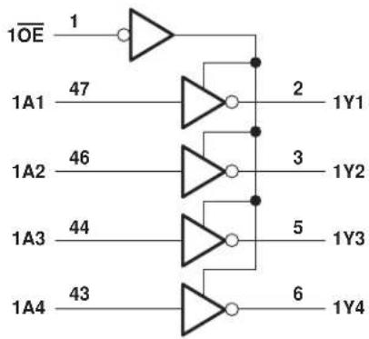
The devices can be used as four 4-bit buffers, two 8-bit buffers, or one 16-bit buffer. The devices provide inverting outputs and symmetrical active-low output-enable (OE) inputs.
When V_CC is between 0 and 1.5 V, the device is in the high-impedance state during power up or power down. However, to ensure the high-impedance state above 1.5 V, should be tied to V_CC through a pullup resistor; the minimum value of the resistor is determined by the current-sinking capability of the driver.
Active bus-hold circuitry is provided to hold unused or floating data inputs at a valid logic level.
The SN54ALVTH16240 is characterized for operation over the full military temperature range of -55^ to 125^ . The SN74ALVTH16240 is characterized for operation from -40^ to 85^ .
FUNCTION TABLE (each 4-bit buffer)
| INPUTS | OUTPUTY | |
| OE | A | |
| L | L | |
| L | L | H |
| H | X | Z |
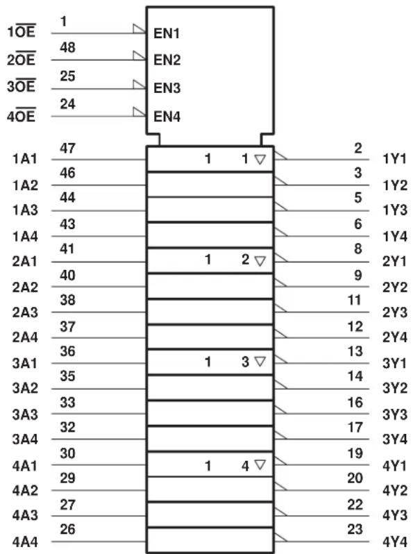
logic symbol†
text_image
1OE 1 EN1 2OE 48 EN2 3OE 25 EN3 4OE 24 EN4 1A1 47 1 1 ▼ 2 1Y1 1A2 46 1A3 44 1A4 43 2A1 41 1 2 ▼ 8 2Y1 2A2 40 2A3 38 2A4 37 3A1 36 1 3 ▼ 13 3Y1 3A2 35 3A3 33 3A4 32 4A1 30 1 4 ▼ 19 4Y1 4A2 29 4A3 27 4A4 26 EN1 EN2 EN3 EN4 1 Y1 3 1Y2 5 1Y3 6 1Y4 8 2Y1 9 2Y2 11 2Y3 12 2Y4 13 14 3Y1 16 3Y2 17 3Y3 19 3Y4 20 4Y1 22 4Y2 23 4Y3 4Y4^ This symbol is in accordance with ANSI/IEEE Std 91-1984 and IEC Publication 617-12.
logic diagram (positive logic)
flowchart
graph TD
    A["1OE"] -->|1| B["NOT"]
    C["1A1"] -->|47| D["NOT"]
    E["1A2"] -->|46| F["NOT"]
    G["1A3"] -->|44| H["NOT"]
    I["1A4"] -->|43| J["NOT"]
    B -->|2| K["1Y1"]
    D -->|3| L["1Y2"]
    F -->|5| M["1Y3"]
    H -->|6| N["1Y4"]

flowchart
graph TD
    A["3OE"] -->|25| B["NOT"]
    C["3A1"] -->|36| D["AND"]
    E["3A2"] -->|35| F["AND"]
    G["3A3"] -->|33| H["AND"]
    I["3A4"] -->|32| J["AND"]
    B -->|13| K["3Y1"]
    D -->|14| L["3Y2"]
    F -->|16| M["3Y3"]
    H -->|17| N["3Y4"]

flowchart
graph TD
    A["20E"] -->|48| B["NOT"]
    C["2A1"] -->|41| D["NOT"]
    E["2A2"] -->|40| F["NOT"]
    G["2A3"] -->|38| H["NOT"]
    I["2A4"] -->|37| J["NOT"]
    B --> K["8"]
    D --> L["9"]
    F --> M["11"]
    H --> N["12"]
    J --> O["2Y1"]
    K --> P["2Y2"]
    L --> Q["2Y3"]
    M --> R["2Y4"]

flowchart
graph TD
    A["4OE"] -->|24| B["NOT"]
    C["4A1"] -->|30| D["AND"]
    E["4A2"] -->|29| F["AND"]
    G["4A3"] -->|27| H["AND"]
    I["4A4"] -->|26| J["AND"]
    B -->|19| K["4Y1"]
    D -->|20| L["4Y2"]
    F -->|22| M["4Y3"]
    H -->|23| N["4Y4"]
absolute maximum ratings over operating free-air temperature range (unless otherwise noted)†
Supply voltage range, V_CC -0.5 V to 4.6 V
Input voltage range, V_I (see Note 1) -0.5 V to 7 V
Voltage range applied to any output in the high-impedance or power-off state, V_O (see Note 1) -0.5 V to 7 V
Voltage range applied to any output in the high state, V_O (see Note 1) -0.5 V to 7 V.....
Output current in the low state, I_O : SN54ALVTH16240 96 mA SN74ALVTH16240 128 mA
Output current in the high state, I_O : SN54ALVTH16240 ....-48 mA SN74ALVTH16240 ....-64 mA
Input clamp current, I_IK ( V_I<0 ) -50 mA
Output clamp current, I_OK ( V_O<0 ) -50 mA
Package thermal impedance, _JA (see Note 2): DGG package 89°C/W
DGV package 93°C/W
DL package 94°C/W
Storage temperature range, T_stg -65°C to 150°C
Stresses beyond those listed under "absolute maximum ratings" may cause permanent damage to the device. These are stress ratings only, and functional operation of the device at these or any other conditions beyond those indicated under "recommended operating conditions" is not implied. Exposure to absolute-maximum-rated conditions for extended periods may affect device reliability.
NOTES: 1. The input and output negative-voltage ratings may be exceeded if the input and output clamp-current ratings are observed.
- The package thermal impedance is calculated in accordance with JESD 51.
recommended operating conditions, V_CC = 2.5 V ± 0.2 V (see Note 3)
| SN54ALVTH16240 SN74ALVTH16240 | UNIT | |||||
| MIN TYP MAX MIN TYP MAX | ||||||
| V_CC | Supply voltage 2.3 2.7 2.3 2.7 V | |||||
| V_IH | High-level input voltage 1.7 1.7 V | |||||
| V_IL | Low-level input voltage 0.7 0.7 V | |||||
| V_I | Input voltage 0 V | CC | 5.5 | 0 V | CC | 5.5 V |
| I_OH | High-level output current -6 -8 mA | |||||
| I_OL | Low-level output current | 6 | 8 mA | |||
| Low-level output current; current duty cycle ≤ 50%; f ≥ 1 kHz | 18 | 24 | ||||
| Δt/Δv | Input transition rise or fall rate | Outputs enabled | 10 | ns/V | ||
| Δt/Δ V_CC | Power-up ramp rate | 200 | 200 | ∞s/V | ||
| T_A | Operating free-air temperature | -55 | 125 | -40 | 85 °C | |
NOTE 3: All unused control inputs of the device must be held at V_CC or GND to ensure proper device operation. Refer to the TI application report, Implications of Slow or Floating CMOS Inputs, literature number SCBA004.
recommended operating conditions, V_CC = 3.3 V ± 0.3 V (see Note 3)
| SN54ALVTH16240 SN74ALVTH16240 | UNIT | |||||
| MIN TYP MAX MIN TYP MAX | ||||||
| V_CC | Supply voltage | 3 3.6 3 3.6 V | ||||
| V_IH | High-level input voltage | 2 | 2 V | |||
| V_IL | Low-level input voltage 0.8 0.8 V | |||||
| V_I | Input voltage 0 V | CC | 5.5 0 V | CC | 5.5 V | |
| I_OH | High-level output current | -24 | -32 | mA | ||
| I_OL | Low-level output current | 24 32 | mA | |||
| Low-level output current; current duty cycle ≤ 50%; f ≥ 1 kHz | 48 | 64 | ||||
| Δt/Δv | Input transition rise or fall rate | Outputs enabled | 10 | 10 | ns/V | |
| Δt/Δ V_CC | Power-up ramp rate | 200 | 200 | ∞s/V | ||
| T_A | Operating free-air temperature | -55 | 125 | -40 | 85 | °C |
NOTE 3: All unused control inputs of the device must be held at V_CC or GND to ensure proper device operation. Refer to the TI application report, Implications of Slow or Floating CMOS Inputs, literature number SCBA004.
electrical characteristics over recommended operating free-air temperature range, V_CC = 2.5 V ± 0.2 V (unless otherwise noted)
| PARAMETER | TEST CONDITIONS | SN54ALVTH16240 SN74ALVTH16240 | UNIT | |||||
| MIN TYP † MAX | MIN TYP † MAX | |||||||
| V_IK | V_CC=2.3 V,I I=-18 mA-1.2-1.2 V | |||||||
| V_OH | V_CC=2.3 V to 2.7 V, I OH=-100 A V | CC-0.2 V | CC-0.2 | V | ||||
| V_CC=2.3 V | I_OH=-6 mA 1.8 | |||||||
| I_OH=-8 mA 1.8 | ||||||||
| V_OL | V_CC=2.3 V to 2.7 V, I OL=100 A 0.2 0.2 | V | ||||||
| V_CC=2.3 V | I_OL=6 mA 0.4 | |||||||
| I_OL=8 mA 0.4 | ||||||||
| I_OL=18 mA | 0.5 | |||||||
| I_OL=24 mA | 0.5 | |||||||
| I_I | Control inputs | V_CC=2.7 V,V I=V_CC or GND | ±1 | ±1 | A | |||
| V_CC=0 or 2.7 V,V_I=5.5 V | 10 | 10 | ||||||
| Data inputs | V_CC=2.7 V | V_I=5.5 V | 10 | 10 | ||||
| V_I=V_CC | 1 | 1 | ||||||
| V_I=0 | -5 | -5 | ||||||
| I_off | V_CC=0,V_I or V_O=0 to 4.5 V | ±100 | A | |||||
| I_BHL^ | V_CC=2.3 V,V I=0.7 V | 115 | 115 | A | ||||
| I_BHH^S | V_CC=2.3 V,V I=1.7 V | -10 | -10 | A | ||||
| I_BHLO^¶ | V_CC=2.7 V,V I=0 to V_CC | 300 | 300 | A | ||||
| I_BHHO^# | V_CC=2.7 V,V I=0 to V_CC | -300 | -300 | A | ||||
| I_EX|| | V_CC=2.3 V,V O=5.5 V | 125 | 125 | A | ||||
| I_OZ(PU/PD)^ | V_CC≤ 1.2 V, V_O=0.5 V to V_CC, V_I=GND or V_CC, =don't care | ±100 | ±100 | A | ||||
| I_OZH | V_CC=2.7 V | V_O=2.3 V, V_I=0.7 V or 1.7 V | 5 | 5 | A | |||
| I_OZL | V_CC=2.7 V | V_O=0.5 V, V_I=0.7 V or 1.7 V | -5 | -5 | A | |||
| I_CC | V_CC=2.7 V, I_O=0, V_I=V_CC or GND | Outputs high | 0.04 0.1 | 0.04 0.1 | mA | |||
| Outputs low | 2.3 4.5 2.3 4.5 | |||||||
| Outputs disabled | 0.04 0.1 | 0.04 0.1 | ||||||
| C_i | V_CC=2.5 V,V I=2.5 V or 0 | 3.5 3.5 | pF | |||||
| C_o | V_CC=2.5 V,V O=2.5 V or 0 | 6 | 6 | pF | ||||
All typical values are at V_CC = 2.5 V , T_A = 25^ C .
The bus-hold circuit can sink at least the minimum low sustaining current at V_IL max. I_BHL should be measured after lowering V_IN to GND and then raising it to V_IL max.
§ The bus-hold circuit can source at least the minimum high sustaining current at V_IH min. I_BHH should be measured after raising V_IN to V_CC and then lowering it to V_IH min.
¶ An external driver must source at least IBHLO to switch this node from low to high.
An external driver must sink at least IBHHO to switch this node from high to low.
|| Current into an output in the high state when V_O > V_CC
★High-impedance state during power up or power down
electrical characteristics over recommended operating free-air temperature range, V_CC = 3.3 V ± 0.3 V (unless otherwise noted)
| PARAMETER | TEST CONDITIONS | SN54ALVTH16240 SN74ALVTH16240 | UNIT | |||||
| MIN TYP † MAX | MIN TYP † MAX | |||||||
| V_IK | V_CC=3 V, I I=-18 mA-1.2-1.2 V | |||||||
| V_OH | V_CC=3 V to 3.6 V, I OH=-100 A V | CC-0.2 V | CC-0.2 | V | ||||
| V_CC=3 V | I_OH=-24 mA 2 | |||||||
| I_OH=-32 mA 2 | ||||||||
| V_OL | V_CC=3 V to 3.6 V, I OL=100 A 0.2 0.2 | V | ||||||
| V_CC=3 V | I_OL=16 mA 0.4 | |||||||
| I_OL=24 mA | 0.5 | |||||||
| I_OL=32 mA 0.5 | ||||||||
| I_OL=48 mA | 0.55 | |||||||
| I_OL=64 mA | 0.55 | |||||||
| I_I | Control inputs | V_CC=3.6 V, V_I=V_CC or GND | ±1 | ±1 | A | |||
| V_CC=0 or 3.6 V, V_I=5.5 V | 10 | 10 | ||||||
| Data inputs | V_CC=3.6 V | V_I=5.5 V | 10 | 10 | ||||
| V_I=V_CC | 1 | 1 | ||||||
| V_I=0 | -5 | -5 | ||||||
| I_off | V_CC=0, V_I or V_O=0 to 4.5 V | ±100 | A | |||||
| I_BHL^ | V_CC=3 V, V_I=0.8 V | 75 | 75 | A | ||||
| I_BHH^S | V_CC=3 V, V_I=2 V | -75 | -75 | A | ||||
| I_BHLO^¶ | V_CC=3.6 V, V_I=0 to V_CC | 500 | 500 | A | ||||
| I_BHHO^# | V_CC=3.6 V, V_I=0 to V_CC | -500 | -500 | A | ||||
| I_EX^|| | V_CC=3 V, V_O=5.5 V | 125 | 125 | A | ||||
| I_OZ(PU/PD)^ | V_CC≤ 1.2 V, V_O=0.5 V to V_CC, V_I=GND or V_CC, =don't care | ±100 | ±100 | A | ||||
| I_OZH | V_CC=3.6 V | V_O=3 V, V_I=0.8 V or 2 V | 5 | 5 | A | |||
| I_OZL | V_CC=3.6 V | V_O=0.5 V, V_I=0.8 V or 2 V | -5 | -5 | A | |||
| I_CC | V_CC=3.6 V,, I_O=0, V_I=V_CC or GND | Outputs high | 0.07 0.1 | 0.07 0.1 | mA | |||
| Outputs low | 3.2 5.5 | 3.2 5 | ||||||
| Outputs disabled | 0.07 0.1 | 0.07 0.1 | ||||||
| CC^ | V_CC=3 V to 3.6 V, One input at V_CC-0.6 V, Other inputs at V_CC or GND | 0.4 0.4 mA | ||||||
| C_i | V_CC=3.3 V, V_I=3.3 V or 0 | 3.5 3.5 | pF | |||||
| C_o | V_CC=3.3 V, V_O=3.3 V or 0 | 6 | 6 | pF | ||||
All typical values are at V_CC = 3.3 V , T_A = 25^ C .
The bus-hold circuit can sink at least the minimum low sustaining current at V_IL max. I_BHL should be measured after lowering V_IN to GND and then raising it to V_IL max.
§ The bus-hold circuit can source at least the minimum high sustaining current at V_IH min. IBHH should be measured after raising V_IN to V_CC and then lowering it to V_IH min.
¶ An external driver must source at least IBHLO to switch this node from low to high.
An external driver must sink at least IBHHO to switch this node from high to low.
|| Current into an output in the high state when V_O > V_CC
★High-impedance state during power up or power down
☐This is the increase in supply current for each input that is at the specified TTL voltage level rather than V_CC or GND.
switching characteristics over recommended operating free-air temperature range, C_L = 30 pF, V_CC = 2.5 V ± 0.2 V (unless otherwise noted) (see Figure 1)
| PARAMETER | FROM TO(INPUT) (OUTPUT) | SN54ALVTH16240 | SN74ALVTH16240 | UNIT | |
| MIN MAX MIN MAX | |||||
| t_PLH | A | Y | 1 3.8 1 3.7 | ns | |
| t_PHL | 1 3.6 1 3.5 | ||||
| t_PZH | Y | 1 5.4 1 5.3 | ns | ||
| t_PZL | 1 4.3 1 4.2 | ||||
| t_PHZ | Y | 1 4.8 1 4.7 | ns | ||
| t_PLZ | 1 3.6 1 3.5 | ||||
switching characteristics over recommended operating free-air temperature range, C_L = 50 pF, V_CC = 3.3 V ± 0.3 V (unless otherwise noted) (see Figure 2)
| PARAMETER | FROM TO(INPUT) (OUTPUT) | SN54ALVTH16240 | SN74ALVTH16240 | UNIT | |
| MIN MAX MIN MAX | |||||
| t_PLH | A | Y | 1 3.4 1 3.3 | ns | |
| t_PHL | 1 3.3 1 3.2 | ||||
| t_PZH | Y | 1 3.8 1 3.7 | ns | ||
| t_PZL | 1 3.2 1 3.1 | ||||
| t_PHZ | Y | 1.4 5.1 1.5 5 | ns | ||
| t_PLZ | 1.4 4.2 1.5 4.1 | ||||
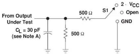
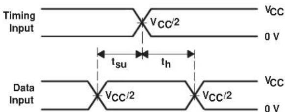
PARAMETER MEASUREMENT INFORMATION
$$ V _ {C C} = 2. 5 \mathrm{V} \pm 0. 2 \mathrm{V} $$
text_image
From Output Under Test CL = 30 pF (see Note A) 500 Ω 500 Ω S1 2 · VCC Open GNDLOAD CIRCUIT
text_image
Timing Input VCC/2 0 V tsu th Data Input VCC/2 VCC/2 0 VVOLTAGE WAVEFORMS SETUP AND HOLD TIMES

text_image
Input VCC/2 VCC/2 0 V tPLH tPHL Output VCC/2 VCC/2 VOH VOLVOLTAGE WAVEFORMS PROPAGATION DELAY TIMES
| TEST S1 | |
| t_PLH/t_PHL | Open |
| t_PLZ/t_PZL | 2 · V_CC |
| t_PHZ/t_PZH | GND |

text_image
Input VCC/2 tw VCC/2 0 V VCCtext_image
Output Control (low-level enabling) VCC/2 VCC/2 0 V tPZL tPLZ Output Waveform 1 S1 at 2 · VCC (see Note B) VCC/2 VOL + 0.15 V VOL tPZH tPHZ Output Waveform 2 S1 at GND (see Note B) VCC/2 VOH - 0.15 V 0 VVOLTAGE WAVEFORMS
ENABLE AND DISABLE TIMES
NOTES: A. C L includes probe and jig capacitance.
B. Waveform 1 is for an output with internal conditions such that the output is low except when disabled by the output control.
Waveform 2 is for an output with internal conditions such that the output is high except when disabled by the output control.
C. All input pulses are supplied by generators having the following characteristics: PRR ≤ 10 MHz, Z O = 50 Ω, t r ≤ 2 ns, t _f ≤ 2 ns.
D. The outputs are measured one at a time with one transition per measurement.
Figure 1. Load Circuit and Voltage Waveforms
PARAMETER MEASUREMENT INFORMATION
$$ V _ {C C} = 3. 3 \mathrm{V} \pm 0. 3 \mathrm{V} $$

text_image
From Output Under Test CL = 50 pF (see Note A) 500 Ω 500 Ω S1 6 V Open GNDLOAD CIRCUIT
| TEST S1 | |
| tPLH/tPHL | Open |
| tPLZ/tPZL | 6 V |
| tPHZ/tPZH | GND |

text_image
Timing Input 1.5 V 3 V 0 V tsu th Data Input 1.5 V 1.5 V 3 V 0 VVOLTAGE WAVEFORMS SETUP AND HOLD TIMES

text_image
Input 1.5 V t_w 1.5 V 3 V 0 VVOLTAGE WAVEFORMS
ENABLE AND DISABLE TIMES
LOW- AND HIGH-LEVEL ENABLING
NOTES: A. C L includes probe and jig capacitance.
B. Waveform 1 is for an output with internal conditions such that the output is low except when disabled by the output control. Waveform 2 is for an output with internal conditions such that the output is high except when disabled by the output control.
C. All input pulses are supplied by generators having the following characteristics: PRR ≤ 10 MHz, Z_O = 50 , t_f ≤ 2.5 ns , t_f ≤ 2.5 ns .
D. The outputs are measured one at a time with one transition per measurement.
Figure 2. Load Circuit and Voltage Waveforms
PACKAGING INFORMATION
| Orderable Device Status(1) | Package Type | Package Drawing | Pins | Package Qty | Eco Plan(2) | Lead finish/ Ball material(6) | MSL Peak Temp(3) | Op Temp (°C) | Device Marking(4,5) | Samples | |
| 74ALVTH16240DLG4 ACTIVE SSOP DL 48 25 RoHS & Green NIPDAU Level-1-260C-UNLIM -40 to 85 ALVTH16240 | Samples | ||||||||||
| SN74ALVTH16240DL ACTIVE SSOP DL 48 25 RoHS & Green NIPDAU Level-1-260C-UNLIM -40 to 85 ALVTH16240 | Samples | ||||||||||
| SN74ALVTH16240GR | ACTIVE | TSSOP | DGG | 48 | 2000 | RoHS & Green | NIPDAU | Level-1-260C-UNLIM | -40 to 85 | ALVTH16240 | Samples |
(1) The marketing status values are defined as follows:
ACTIVE: Product device recommended for new designs.
LIFEBUY: TI has announced that the device will be discontinued, and a lifetime-buy period is in effect.
NRND: Not recommended for new designs. Device is in production to support existing customers, but TI does not recommend using this part in a new design.
PREVIEW: Device has been announced but is not in production. Samples may or may not be available.
OBSOLETE: TI has discontinued the production of the device.
(2) RoHS: TI defines "RoHS" to mean semiconductor products that are compliant with the current EU RoHS requirements for all 10 RoHS substances, including the requirement that RoHS substance do not exceed 0.1% by weight in homogeneous materials. Where designed to be soldered at high temperatures, "RoHS" products are suitable for use in specified lead-free processes. TI may reference these types of products as "Pb-Free".
RoHS Exempt: TI defines "RoHS Exempt" to mean products that contain lead but are compliant with EU RoHS pursuant to a specific EU RoHS exemption.
Green: TI defines "Green" to mean the content of Chlorine (Cl) and Bromine (Br) based flame retardants meet JS709B low halogen requirements of <=1000ppm threshold. Antimony trioxide based flame retardants must also meet the <=1000ppm threshold requirement.
(3) MSL, Peak Temp. - The Moisture Sensitivity Level rating according to the JEDEC industry standard classifications, and peak solder temperature.
(4) There may be additional marking, which relates to the logo, the lot trace code information, or the environmental category on the device.
(5) Multiple Device Markings will be inside parentheses. Only one Device Marking contained in parentheses and separated by a "\~" will appear on a device. If a line is indented then it is a continuation of the previous line and the two combined represent the entire Device Marking for that device.
(6) Lead finish/Ball material - Orderable Devices may have multiple material finish options. Finish options are separated by a vertical ruled line. Lead finish/Ball material values may wrap to two lines if the finish value exceeds the maximum column width.
Important Information and Disclaimer: The information provided on this page represents TI's knowledge and belief as of the date that it is provided. TI bases its knowledge and belief on information provided by third parties, and makes no representation or warranty as to the accuracy of such information. Efforts are underway to better integrate information from third parties. TI has taken and continues to take reasonable steps to provide representative and accurate information but may not have conducted destructive testing or chemical analysis on incoming materials and chemicals. TI and TI suppliers consider certain information to be proprietary, and thus CAS numbers and other limited information may not be available for release.

www.ti.com
TEXAS
INSTRUMENTS
PACKAGE OPTION ADDENDUM
10-Dec-2020
In no event shall TI's liability arising out of such information exceed the total purchase price of the TI part(s) at issue in this document sold by TI to Customer on an annual basis.
TAPE AND REEL INFORMATION

*All dimensions are nominal
| Device Package | Type | Package Drawing | Pins | SPQ Reel | Diameter (mm) | Reel Width W1 (mm) | A0 (mm) | B0 (mm) | K0 (mm) | P1 (mm) | W (mm) | Pin1 Quadrant |
| SN74ALVTH16240GR T | SSOP DG | G 48 2000 | 330.0 | 24.4 8.6 1 | 3.0 1.8 12 | 0 24.0 Q1 |

text_image
TAPE AND REEL BOX DIMENSIONS W L*All dimensions are nominal
| Device | Package Type | Package Drawing | Pins | SPQ | Length (mm) | Width (mm) | Height (mm) |
| SN74ALVTH16240GR T$ | SOP DGG 48 2000 | 367.0 367.0 45.0 |
TUBE
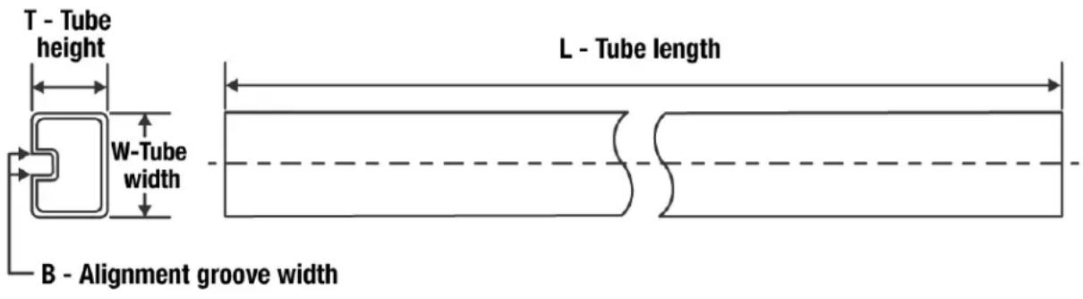
text_image
T - Tube height L - Tube length W-Tube width B - Alignment groove width*All dimensions are nominal
| Device | Package Name | Package Type | Pins | SPQ | L (mm) | W (mm) | T (μm) | B (mm) |
| 74ALVTH16240DLG4 DL | SSOP 48 25 473.7 | 14.24 5110 7.87 | ||||||
| SN74ALVTH16240DL DL | SSOP 48 25 473.7 | 14.24 5110 7.87 |
DL (R-PDSO-G48)
PLASTIC SMALL-OUTLINE PACKAGE

text_image
0.025 (0,635) 48 0.0135 (0,343) 0.008 (0,203) 0.005 (0,13) 25 0.420 (10,67) 0.395 (10,03) 0.299 (7,59) 0.291 (7,39) 1 24 0.630 (16,00) 0.620 (15,75) 0.010 (0,25) 0.005 (0,13) Gage Plane 0°-8° 0.010 (0,25) 0.040 (1,02) 0.020 (0,51) Seating Plane 0.110 (2,79) MAX 0.008 (0,20) MIN Seating Plane 0.004 (0,10) 4040048-3/F 05/13NOTES: A. All linear dimensions are in inches (millimeters).
B. This drawing is subject to change without notice.
C. Body dimensions do not include mold flash or protrusion not to exceed 0.006 (0,15).
D. Falls within JEDEC MO-118
PowerPAD is a trademark of Texas Instruments.
SMALL OUTLINE PACKAGE
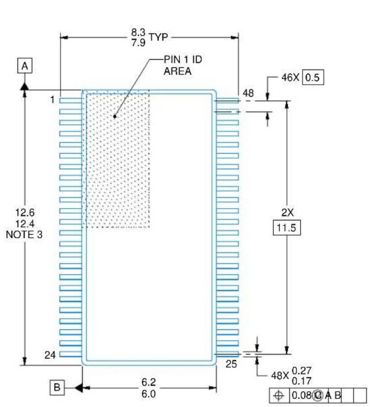
text_image
8.3 TYP 7.9 PIN 1 ID AREA 46X 0.5 1 48 12.6 12.4 NOTE 3 2X 11.5 24 25 48X 0.27 0.17 B 6.2 6.0 ⊕ 0.08@ A B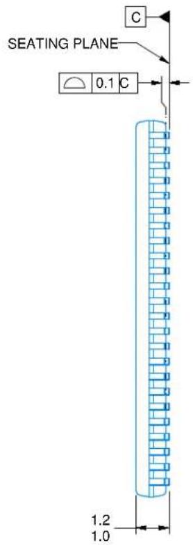
text_image
SEATING PLANE 0.1 C C 1.2 1.0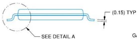
text_image
SEE DETAIL A (0.15) TYP GA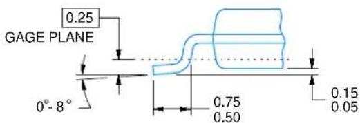
text_image
GAGE PLANE 0° - 8° 0.25 0.75 0.50 0.15 0.05DETAIL A TYPICAL
4214859/B 11/2020
NOTES:
- All linear dimensions are in millimeters. Any dimensions in parenthesis are for reference only. Dimensioning and tolerancing per ASME Y14.5M.
- This drawing is subject to change without notice.
- This dimension does not include mold flash, protrusions, or gate burrs. Mold flash, protrusions, or gate burrs shall not exceed 0.15 mm per side.
- Reference JEDEC registration MO-153.
SMALL OUTLINE PACKAGE
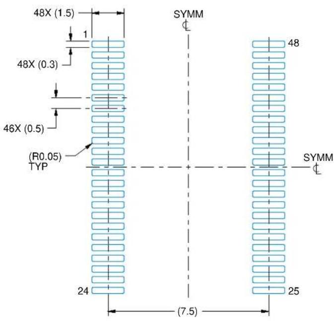
text_image
48X (1.5) 1 48X (0.3) 46X (0.5) (R0.05) TYP 24 SYMM 48 SYMM 25 (7.5)LAND PATTERN EXAMPLE SCALE:6X

text_image
SOLDER MASK OPENING METAL 0.05 MAX ALL AROUNDNON SOLDER MASK DEFINED
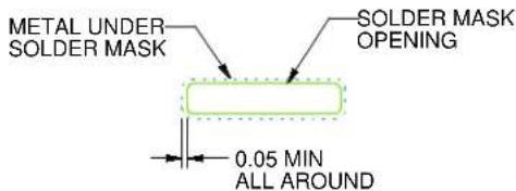
text_image
METAL UNDER SOLDER MASK SOLDER MASK OPENING 0.05 MIN ALL AROUNDSOLDER MASK
DEFINED
SOLDER MASK DETAILS
4214859/B 11/2020
NOTES: (continued)
- Publication IPC-7351 may have alternate designs.
- Solder mask tolerances between and around signal pads can vary based on board fabrication site.
SMALL OUTLINE PACKAGE
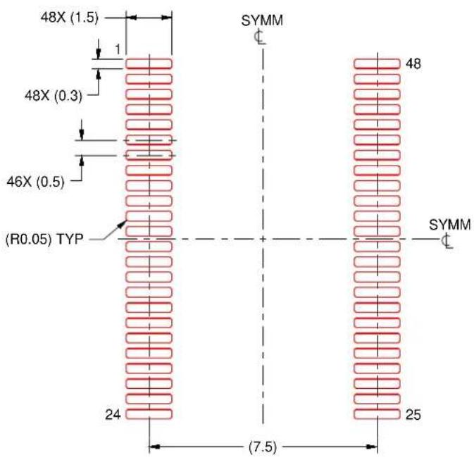
text_image
48X (1.5) 1 48X (0.3) 46X (0.5) (R0.05) TYP 24 SYMM 48 SYMM 25 (7.5)SOLDER PASTE EXAMPLE BASED ON 0.125 mm THICK STENCIL SCALE:6X
4214859/B 11/2020
NOTES: (continued)
- Laser cutting apertures with trapezoidal walls and rounded corners may offer better paste release. IPC-7525 may have alternate design recommendations.
- Board assembly site may have different recommendations for stencil design.
DGG (R-PDSO-G\*\*) PLASTIC SMALL-OUTLINE PACKAGE
48 PINS SHOWN

text_image
0,50 48 0,27 0,17 ⊕ 0,08 Ⓜ 25 6,20 6,00 8,30 7,90 1 24 A 0,15 NOM Gage Plane 0,25 0°-8° 0,75 0,50 1,20 MAX Seating Plane 0,10 PINS ** DIM 48 56 64 A MAX 12,60 14,10 17,10 A MIN 12,40 13,90 16,90 4040078/F 12/97NOTES: A. All linear dimensions are in millimeters.
B. This drawing is subject to change without notice.
C. Body dimensions do not include mold protrusion not to exceed 0,15.
D. Falls within JEDEC MO-153
IMPORTANT NOTICE AND DISCLAIMER
TI PROVIDES TECHNICAL AND RELIABILITY DATA (INCLUDING DATA SHEETS), DESIGN RESOURCES (INCLUDING REFERENCE DESIGNS), APPLICATION OR OTHER DESIGN ADVICE, WEB TOOLS, SAFETY INFORMATION, AND OTHER RESOURCES "AS IS" AND WITH ALL FAULTS, AND DISCLAIMS ALL WARRANTIES, EXPRESS AND IMPLIED, INCLUDING WITHOUT LIMITATION ANY IMPLIED WARRANTIES OF MERCHANTABILITY, FITNESS FOR A PARTICULAR PURPOSE OR NON-INFRINGEMENT OF THIRD PARTY INTELLECTUAL PROPERTY RIGHTS.
These resources are intended for skilled developers designing with TI products. You are solely responsible for (1) selecting the appropriate TI products for your application, (2) designing, validating and testing your application, and (3) ensuring your application meets applicable standards, and any other safety, security, regulatory or other requirements.
These resources are subject to change without notice. TI grants you permission to use these resources only for development of an application that uses the TI products described in the resource. Other reproduction and display of these resources is prohibited. No license is granted to any other TI intellectual property right or to any third party intellectual property right. TI disclaims responsibility for, and you will fully indemnify TI and its representatives against, any claims, damages, costs, losses, and liabilities arising out of your use of these resources.
TI's products are provided subject to TI's Terms of Sale or other applicable terms available either on ti.com or provided in conjunction with such TI products. TI's provision of these resources does not expand or otherwise alter TI's applicable warranties or warranty disclaimers for TI products.
TI objects to and rejects any additional or different terms you may have proposed.
Mailing Address: Texas Instruments, Post Office Box 655303, Dallas, Texas 75265
Copyright © 2022, Texas Instruments Incorporated