SN74LVTH16501DL - Electronic component TEXAS INSTRUMENTS - Free user manual and instructions
Find the device manual for free SN74LVTH16501DL TEXAS INSTRUMENTS in PDF.

User questions about SN74LVTH16501DL TEXAS INSTRUMENTS
0 question about this device. Answer the ones you know or ask your own.
Ask a new question about this device
Download the instructions for your Electronic component in PDF format for free! Find your manual SN74LVTH16501DL - TEXAS INSTRUMENTS and take your electronic device back in hand. On this page are published all the documents necessary for the use of your device. SN74LVTH16501DL by TEXAS INSTRUMENTS.
USER MANUAL SN74LVTH16501DL TEXAS INSTRUMENTS
●Members of the Texas Instruments Widebus™ Family
- UBT™ Transceiver Combines D-Type Latches and D-Type Flip-Flops for Operation in Transparent, Latched, or Clocked Mode
●State-of-the-Art Advanced BiCMOS Technology (ABT) Design for 3.3-V Operation and Low Static-Power Dissipation
●Support Mixed-Mode Signal Operation (5-V Input and Output Voltages With 3.3-V VCC)
●Support Unregulated Battery Operation Down to 2.7 V
●Typical V OLP (Output Ground Bounce)
<0.8 V at V_CC = 3.3 V, T_A = 25^
●I off and Power-Up 3-State Support Hot Insertion
●Bus Hold on Data Inputs Eliminates the Need for External Pullup/Pulldown Resistors
●Distributed V CC and GND Pins Minimize High-Speed Switching Noise
●Flow-Through Architecture Optimizes PCB Layout
●Latch-Up Performance Exceeds 500 mA Per JESD 17
- ESD Protection Exceeds JESD 22
- 2000-V Human-Body Model (A114-A)
- 200-V Machine Model (A115-A)
SN54LVTH16501 ... WD PACKAGE SN74LVTH16501 ... DGG OR DL PACKAGE (TOP VIEW)
| OEAB | 1 | 56 | GND |
| LEAB | 2 | 55 | CLKAB |
| A1 | 3 | 54 | B1 |
| GND | 4 | 53 | GND |
| A2 | 5 | 52 | B2 |
| A3 | 6 | 51 | B3 |
| V_CC | 7 | 50 | V_CC |
| A4 | 8 | 49 | B4 |
| A5 | 9 | 48 | B5 |
| A6 | 10 | 47 | B6 |
| GND | 11 | 46 | GND |
| A7 | 12 | 45 | B7 |
| A8 | 13 | 44 | B8 |
| A9 | 14 | 43 | B9 |
| A10 | 15 | 42 | B10 |
| A11 | 16 | 41 | B11 |
| A12 | 17 | 40 | B12 |
| GND | 18 | 39 | GND |
| A13 | 19 | 38 | B13 |
| A14 | 20 | 37 | B14 |
| A15 | 21 | 36 | B15 |
| V_CC | 22 | 35 | V_CC |
| A16 | 23 | 34 | B16 |
| A17 | 24 | 33 | B17 |
| GND | 25 | 32 | GND |
| A18 | 26 | 31 | B18 |
| OEBA | 27 | 30 | CLKBA |
| LEBA | 28 | 29 | GND |
description/ordering information
The 'LVTH16501 devices are 18-bit universal bus transceivers designed for low-voltage (3.3-V) V_CC operation, but with the capability to provide a TTL interface to a 5-V system environment.
ORDERING INFORMATION
| TA | PACKAGE^ | ORDERABLEPART NUMBER | TOP-SIDEMARKING | |
| -40°C to 85°C | SSOP - DL | Tube SN74LVTH16501DL | H16501DL | LVTH16501 |
| Tape and reel SN74LVTH16501DLR | ||||
| TSSOP - DGG Tape and | reel SN74LVTH16501DGGR LVTH16501 | 16501DGGR LVTH16501 | ||
| -55°C to 125°C | CFP - WD | Tube | SNJ54LVTH16501WD | SNJ54LVTH16501WD |
† Package drawings, standard packing quantities, thermal data, symbolization, and PCB design guidelines are available at www.ti.com/sc/package.

Please be aware that an important notice concerning availability, standard warranty, and use in critical applications of Texas Instruments semiconductor products and disclaimers thereto appears at the end of this data sheet.
Widebus and UBT are trademarks of Texas Instruments.
PRODUCTIONDATAinformationiscurrentasofpublicationdate. Products conform to specifications per the terms of Texas Instruments standard warranty. Production processing does not necessarily include testing of all parameters.

TEXAS
INSTRUMENTS
POST OFFICE BOX 655303 ● DALLAS, TEXAS 75265
Copyright © 2002, Texas Instruments Incorporated On products compliant to MIL-PRF-38535, all parameters are tested unless otherwise noted. On all other products, production processing does not necessarily include testing of all parameters.
description/ordering information (continued)
Data flow in each direction is controlled by output-enable (OEAB and OEBA), latch-enable (LEAB and LEBA), and clock (CLKAB and CLKBA) inputs. For A-to-B data flow, the devices operate in the transparent mode when LEAB is high. When LEAB is low, the A data is latched if CLKAB is held at a high or low logic level. If LEAB is low, the A data is stored in the latch/flip-flop on the low-to-high transition of CLKAB. When OEAB is high, the outputs are active. When OEAB is low, the outputs are in the high-impedance state.
Data flow for B to A is similar to that of A to B but uses , LEBA, and CLKBA. The output enables are complementary (OEAB is active high and is active low).
Active bus-hold circuitry holds unused or undriven inputs at a valid logic state. Use of pullup or pulldown resistors with the bus-hold circuitry is not recommended.
When V_CC is between 0 and 1.5 V, the devices are in the high-impedance state during power up or power down. However, to ensure the high-impedance state above 1.5 V, OE should be tied to V_CC through a pullup resistor and OE should be tied to GND through a pulldown resistor; the minimum value of the resistor is determined by the current-sinking/current-sourcing capability of the driver.
These devices are fully specified for hot-insertion applications using I_off and power-up 3-state. The I_off circuitry disables the outputs, preventing damaging current backflow through the devices when they are powered down. The power-up 3-state circuitry places the outputs in the high-impedance state during power up and power down, which prevents driver conflict.
FUNCTION TABLET
| INPUTS | OUTPUTB | |||
| OEAB LEAB CLKAB A | ||||
| L X X X Z | ||||
| H H | X | L | L | |
| H H | X | H | H | |
| H L ↑ L | L | |||
| H L ↑ H | H | |||
| H L | H | X | B | 0^‡ |
| H L L X | B | 0^§ | ||
^ A-to-B data flow is shown; B-to-A flow is similar, but uses OEBA, LEBA, and CLKBA.
Output level before the indicated steady-state input conditions were established, provided that CLKAB was high before LEAB went low
§ Output level before the indicated steady-state input conditions were established
logic diagram (positive logic)

flowchart
graph TD
    OEAB["OEAB"] -->|1| NOT1["NOT"]
    CLKAB["CLKAB"] -->|55| NOT2["NOT"]
    LEAB["LEAB"] -->|2| NOT3["NOT"]
    LEBA["LEBA"] -->|28| NOT4["NOT"]
    CLKBA["CLKBA"] -->|30| NOT5["NOT"]
    OEBA_bar["OEBA"] -->|27| NOT6["NOT"]
    A1["A1"] -->|3| NOT7["NOT"]
    NOT1 --> FF1["FF1"]
    NOT2 --> FF2["FF2"]
    NOT3 --> FF3["FF3"]
    NOT4 --> FF4["FF4"]
    NOT5 --> FF5["FF5"]
    NOT6 --> FF6["FF6"]
    NOT7 --> FF7["FF7"]
    FF1 --> C1["C1 CLK"]
    FF2 --> C1
    FF3 --> C1
    FF4 --> C1
    FF5 --> C1
    FF6 --> C1
    FF7 --> C1
    FF8 --> C1
    FF9 --> C1
    FF10 --> C1
    FF11 --> C1
    FF12 --> C1
    FF13 --> C1
    FF14 --> C1
    FF15 --> C1
    FF16 --> C1
    FF17 --> C1
    FF18 --> C1
    FF19 --> C1
    FF20 --> C1
    FF21 --> C1
    FF22 --> C1
    FF23 --> C1
    FF24 --> C1
    FF25 --> C1
    FF26 --> C1
    FF27 --> C1
    FF28 --> C1
    FF29 --> C1
    FF30 --> C1
    FF31 --> C1
    FF32 --> C1
    FF33 --> C1
    FF34 --> C1
    FF35 --> C1
    FF36 --> C1
    FF37 --> C1
    FF38 --> C1
    FF39 --> C1
    FF40 --> C1
    FF41 --> C1
    FF42 --> C1
    FF43 --> C1
    FF44 --> C1
    FF45 --> C1
    FF46 --> C1
    FF47 --> C1
    FF48 --> C1
    FF49 --> C1
    FF50 --> C1
    FF51 --> C1
    FF52 --> C1
    FF53 --> C1
    FF54 --> C1
    B1["B1"] --> C1
    A1 --> FF7
    A2 --> FF8
    A3 --> FF9
    A4 --> FF10
    A5 --> FF11
    A6 --> FF12
    A7 --> FF13
    A8 --> FF14
    A9 --> FF15
    A10 --> FF16
    A11 --> FF17
    A12 --> FF18
    A13 --> FF19
    A14 --> FF20
    A15 --> FF21
    A16 --> FF22
    A17 --> FF23
    A18 --> FF24
    A19 --> FF25
    A20 --> FF26
    A21 --> FF27
    A22 --> FF28
    A23 --> FF29
    A24 --> FF30
    A25 --> FF31
    A26 --> FF32
    A27 --> FF33
    A28 --> FF34
    A29 --> FF35
    A30 --> FF36
    A31 --> FF37
    A32 --> FF38
    A33 --> FF39
    A34 --> FF40
    A35 --> FF41
    A36 --> FF42
    A37 --> FF43
    A38 --> FF44
    A39 --> FF45
    A40 --> FF46
    A41 --> FF47
    A42 --> FF48
    A43 --> FF49
    A44 --> FF50
To 17 Other Channels
absolute maximum ratings over operating free-air temperature range (unless otherwise noted) ^†
Supply voltage range, V_CC -0.5 V to 4.6 V
Input voltage range, V_I (see Note 1) -0.5 V to 7 V
Voltage range applied to any output in the high-impedance or power-off state, V_O (see Note 1) -0.5 V to 7 V
Voltage range applied to any output in the high state, V_O (see Note 1) -0.5 V to V CC + 0.5 V.
Current into any output in the low state, I_O : SN74LVTH16501 SN54LVTH16501 128
Current into any output in the high state, I_O (see Note 2): SN54LVTH16501 48 mA
SN74LVTH16501 64 mA
Input clamp current, I_IK ( V_I<0 ) -50 mA
Output clamp current, I_OK ( V_O < 0 ) -50 mA
Package thermal impedance, _JA (see Note 3): DGG package 64^ / W
DL package 56°C/W
Storage temperature range, T_stg -65^ to 150^
Stresses beyond those listed under "absolute maximum ratings" may cause permanent damage to the device. These are stress ratings only, and functional operation of the device at these or any other conditions beyond those indicated under "recommended operating conditions" is not implied. Exposure to absolute-maximum-rated conditions for extended periods may affect device reliability.
NOTES: 1. The input and output negative-voltage ratings may be exceeded if the input and output clamp-current ratings are observed.
-
This current flows only when the output is in the high state and V_O > V_CC .
-
The package thermal impedance is calculated in accordance with JESD 51-7.
recommended operating conditions (see Note 4)
| SN54LVTH16501 | SN74LVTH16501 | UNIT | ||
| MIN MAX MIN | MAX | |||
| V_CC Supply voltage 2.7 3.6 2.7 3.6 V | ||||
| V_IH High-level input voltage 2 2 V | ||||
| V_IL Low-level input voltage 0.8 0.8 V | ||||
| V_I Input voltage 5.5 5.5 V | ||||
| I_OH High-level output current -24 -32 mA | ||||
| I_OL Low-level output current | 48 | 64 | mA | |
| t/ v Input transition rise or fall rate | Outputs enabled | 10 | 10 | ns/V |
| t/ V_CC Power-up ramp rate | 200 | 200 | μs/V | |
| T_A Operating free-air temperature | -55 125 | -40 85 | °C | |
NOTE 4: All unused control inputs of the device must be held at VCC or GND to ensure proper device operation. Refer to the TI application report, Implications of Slow or Floating CMOS Inputs, literature number SCBA004.
electrical characteristics over recommended operating free-air temperature range (unless otherwise noted)
| PARAMETER | TEST CONDITIONS | SN54LVTH16501 SN74LVTH16501 | UNIT | |||||
| MIN TYP † MAX | MIN TYP † MAX | |||||||
| V_IK | V_CC=2.7 V,I I=-18 mA-1.2-1.2 V | |||||||
| V_OH | V_CC=2.7 V to 3.6 V, I OH=-100 A V | CC-0.2 V | CC-0.2 | V | ||||
| V_CC=2.7 V, I OH=-8 mA 2.4 2.4 | ||||||||
| V_CC=3 V | I_OH=-24 mA 2 | |||||||
| I_OH=-32 mA | 2 | |||||||
| V_OL | V_CC=2.7 V | I_OL=100 A | 0.2 | 0.2 | V | |||
| I_OL=24 mA | 0.5 | 0.5 | ||||||
| V_CC=3 V | I_OL=16 mA | 0.4 | 0.4 | |||||
| I_OL=32 mA | 0.5 | 0.5 | ||||||
| I_OL=48 mA | 0.55 | |||||||
| I_OL=64 mA | 0.55 | |||||||
| I | Control inputs | V_CC=3.6 V,V I=V_CC or GND | ±1 | ±1 | μA | |||
| V_CC=0 or 3.6 V, V_I=5.5 V | 10 | 10 | ||||||
| A or B ports‡ | V_CC=3.6 V | V_I=5.5 V | 120 | 20 | ||||
| V_I=V_CC | 1 | 1 | ||||||
| V_I=0 | -5 | -5 | ||||||
| I_off | V_CC=0, V_I or V_O=0 to 4.5 V | ±100 | μA | |||||
| I_(hold) | A or B ports | V_CC=3 V | V_I=0.8 V 75 | 75 | μA | |||
| V_I=2 V | -75 | -75 | ||||||
| V_CC=3.6 V S, V_I=0 to 3.6 V | ±500 | |||||||
| I_OZPU | V_CC=0 to 1.5 V, V_O=0.5 V to 3 V, /OE=don't care | ±100* | ±100 | μA | ||||
| I_OZPD | V_CC=1.5 V to 0, V_O=0.5 V to 3 V, /OE=don't care | ±100* | ±100 | μA | ||||
| I_CC | V_CC=3.6 V, I_O=0, V_I=V_CC or GND | Outputs high | 0.19 | 0.19 | mA | |||
| Outputs low | 5 | 5 | ||||||
| Outputs disabled | 0.19 | 0.19 | ||||||
| I_CC ¶ | V_CC=3 V to 3.6 V, One input at V_CC-0.6 V, Other inputs at V_CC or GND | 0.2 | 0.2 | mA | ||||
| C_i | V_I=3 V or 0 | 4 | 4 | pF | ||||
| C_io | V_O=3 V or 0 | 10 | 10 | pF | ||||
* On products compliant to MIL-PRF-38535, this parameter is not production tested.
All typical values are at V_CC = 3.3 V , T_A = 25^ C .
‡ Unused pins at VCC or GND
§ This is the bus-hold maximum dynamic current. It is the minimum overdrive current required to switch the input from one state to another.
¶ This is the increase in supply current for each input that is at the specified TTL voltage level rather than V_CC or GND.
timing requirements over recommended operating free-air temperature range (unless otherwise noted) (see Figure 1)
| SN54LVTH16501 SN74LVTH16501 | UNIT | ||||||
| V_CC=3.3 V± 0.3 V | V_CC=2.7 V | V_CC=3.3 V± 0.3 V | V_CC=2.7 V | ||||
| MIN MAX MIN | MAX MIN MAX | MIN MAX | |||||
| f_clock | Clock frequency 150 150 150 150 MHz | ||||||
| t_w | Pulse duration | LE high 3.3 3.3 3.3 3.3 | ns | ||||
| CLK high or low | 3.3 3.3 3.3 3 | 3 | |||||
| t_su | Setup time | A before CLKAB↑ 2.5 2.8 2.1 2.4 | ns | ||||
| B before CLKBA↑ 2.5 2.8 2.1 2.4 | |||||||
| A or B before LE↓ | CLK high | 3.4 2.8 2.4 1 | 6 | ||||
| CLK low | 2.2 1.3 1.4 0 | 5 | |||||
| t_h | Hold time | A or B after CLK↑ 2.2 1.5 1 0 | ns | ||||
| A or B after LE↓ | 2.1 1.9 1.7 1 | 7 | |||||
switching characteristics over recommended operating free-air temperature range, C_L = 50 pF (unless otherwise noted) (see Figure 1)
| PARAMETER | FROM(INPUT) | TO(OUTPUT) | SN54LVTH16501 SN74LVTH16501 | UNIT | ||||||
| VCC=3.3 V±0.3 V | VCC=2.7 V | VCC=3.3 V±0.3 V | VCC=2.7 V | |||||||
| MIN MAX MIN | MAX MIN TYP | † | MAX MIN MAX | |||||||
| fmax | 150 | 150 150 | 150 | MHz | ||||||
| tPLH | B or A | A or B | 1.2 | 4.3 | 4.7 | 1.3 | 2.7 | 3.7 | 4 | ns |
| tPHL | 1.2 | 4.3 | 4.6 | 1.3 | 2.4 | 3.7 | 4 | |||
| tPLH | LEBA or LEAB | A or B | 1.4 | 6.2 | 6.6 | 1.5 | 3.4 | 5.1 | 5.7 | ns |
| tPHL | 1.4 | 5.9 | 6.5 | 1.5 | 3.5 | 5.1 | 5.7 | |||
| tPLH | CLKBA orCLKAB | A or B | 1.2 | 6 | 6.7 | 1.3 | 3.5 | 5.1 | 5.7 | ns |
| tPHL | 1.2 | 5.9 | 6.6 | 1.3 | 3.4 | 5.1 | 5.7 | |||
| tPZH | OEBA or OEAB | A or B | 1.2 | 5.5 | 5.9 | 1.3 | 3.4 | 4.8 | 5.5 | ns |
| tPZL | 1.2 | 5.5 | 5.9 | 1.3 | 3.4 | 4.8 | 5.5 | |||
| tPHZ | OEBA or OEAB | A or B | 1.6 | 6.3 | 6.7 | 1.7 | 4.2 | 5.8 | 6.3 | ns |
| tPLZ | 1.6 | 6.1 | 6.6 | 1.7 | 3.8 | 5.8 | 6.3 | |||
All typical values are at V_CC = 3.3 V , T_A = 25^ C .
PARAMETER MEASUREMENT INFORMATION
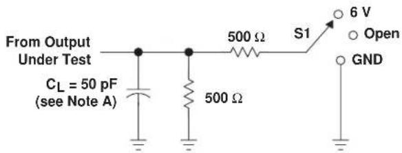
text_image
From Output Under Test CL = 50 pF (see Note A) 500 Ω 500 Ω S1 6 V Open GNDLOAD CIRCUIT
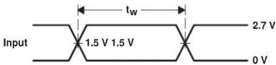
text_image
Input 1.5 V 1.5 V tw 2.7 V 0 VVOLTAGE WAVEFORMS
ENABLE AND DISABLE TIMES
LOW- AND HIGH-LEVEL ENABLING
NOTES: A. C includes probe and jig capacitance.
B. Waveform 1 is for an output with internal conditions such that the output is low except when disabled by the output control. Waveform 2 is for an output with internal conditions such that the output is high except when disabled by the output control.
C. All input pulses are supplied by generators having the following characteristics: PRR ≤ 10 MHz, Z O = 50 Ω, t r ≤ 2.5 ns, t _f ≤ 2.5 ns.
D. The outputs are measured one at a time with one transition per measurement.
E. All parameters and waveforms are not applicable to all devices.
Figure 1. Load Circuit and Voltage Waveforms

TEXAS
INSTRUMENTS
www.ti.com
PACKAGE OPTION ADDENDUM
14-Feb-2021
PACKAGING INFORMATION
| Orderable Device Status(1) | Package Type | Package Drawing | Pins | Package Qty | Eco Plan(2) | Lead finish/ Ball material(6) | MSL Peak Temp(3) | Op Temp (°C) | Device Marking(4-5) | Samples | |
| 74LVTH16501DGGRE4 ACTIVE TSSOP DGG 56 2000 RoHS & Green NIPDAU Level-1-260C-UNLIM -40 to 85 LVTH16501 | Samples | ||||||||||
| 74LVTH16501DLRG4 | ACTIVE | SSOP | DL | 56 | 1000 | RoHS & Green | NIPDAU | Level-1-260C-UNLIM | -40 to 85 | LVTH16501 | Samples |
| SN74LVTH16501DGGR | ACTIVE | TSSOP | DGG | 56 | 2000 | RoHS & Green | NIPDAU | Level-1-260C-UNLIM | -40 to 85 | LVTH16501 | Samples |
| SN74LVTH16501DL | ACTIVE | SSOP | DL | 56 | 20 | RoHS & Green | NIPDAU | Level-1-260C-UNLIM | -40 to 85 | LVTH16501 | Samples |
| SN74LVTH16501DLG4 | ACTIVE | SSOP | DL | 56 | 20 | RoHS & Green | NIPDAU | Level-1-260C-UNLIM | -40 to 85 | LVTH16501 | Samples |
| SN74LVTH16501DLR | ACTIVE | SSOP | DL | 56 | 1000 | RoHS & Green | NIPDAU | Level-1-260C-UNLIM | -40 to 85 | LVTH16501 | Samples |
(1) The marketing status values are defined as follows:
ACTIVE: Product device recommended for new designs.
LIFEBUY: TI has announced that the device will be discontinued, and a lifetime-buy period is in effect.
NRND: Not recommended for new designs. Device is in production to support existing customers, but TI does not recommend using this part in a new design.
PREVIEW: Device has been announced but is not in production. Samples may or may not be available.
OBSOLETE: TI has discontinued the production of the device.
(2) RoHS: TI defines "RoHS" to mean semiconductor products that are compliant with the current EU RoHS requirements for all 10 RoHS substances, including the requirement that RoHS substance do not exceed 0.1% by weight in homogeneous materials. Where designed to be soldered at high temperatures, "RoHS" products are suitable for use in specified lead-free processes. TI may reference these types of products as "Pb-Free".
RoHS Exempt: TI defines "RoHS Exempt" to mean products that contain lead but are compliant with EU RoHS pursuant to a specific EU RoHS exemption.
Green: TI defines "Green" to mean the content of Chlorine (Cl) and Bromine (Br) based flame retardants meet JS709B low halogen requirements of <=1000ppm threshold. Antimony trioxide based flame retardants must also meet the <=1000ppm threshold requirement.
(3) MSL, Peak Temp. - The Moisture Sensitivity Level rating according to the JEDEC industry standard classifications, and peak solder temperature.
(4) There may be additional marking, which relates to the logo, the lot trace code information, or the environmental category on the device.
(5) Multiple Device Markings will be inside parentheses. Only one Device Marking contained in parentheses and separated by a "\~" will appear on a device. If a line is indented then it is a continuation of the previous line and the two combined represent the entire Device Marking for that device.
(6) Lead finish/Ball material - Orderable Devices may have multiple material finish options. Finish options are separated by a vertical ruled line. Lead finish/Ball material values may wrap to two lines if the finish value exceeds the maximum column width.

TEXAS INSTRUMENTS
www.ti.com
PACKAGE OPTION ADDENDUM
14-Feb-2021
Important Information and Disclaimer: The information provided on this page represents TI's knowledge and belief as of the date that it is provided. TI bases its knowledge and belief on information provided by third parties, and makes no representation or warranty as to the accuracy of such information. Efforts are underway to better integrate information from third parties. TI has taken and continues to take reasonable steps to provide representative and accurate information but may not have conducted destructive testing or chemical analysis on incoming materials and chemicals. TI and TI suppliers consider certain information to be proprietary, and thus CAS numbers and other limited information may not be available for release.
In no event shall TI's liability arising out of such information exceed the total purchase price of the TI part(s) at issue in this document sold by TI to Customer on an annual basis.
OTHER QUALIFIED VERSIONS OF SN54LVTH16501, SN74LVTH16501 :
• Catalog: SN74LVTH16501
• Military: SN54LVTH16501
NOTE: Qualified Version Definitions:
• Catalog - TI's standard catalog product
• Military - QML certified for Military and Defense Applications
TAPE AND REEL INFORMATION

*All dimensions are nominal
| Device Package | Type | Package Drawing | Pins | SPQ Reel | Diameter (mm) | Reel Width W1 (mm) | A0 (mm) | B0 (mm) | K0 (mm) | P1 (mm) | W (mm) | Pin1 Quadrant |
| SN74LVTH16501DGGR | TSSOP DG | GG 56 2000 | 330.0 | 24.4 8.6 | 15.6 1.8 12 | .0 24.0 Q1 | ||||||
| SN74LVTH16501DLR S | SOP DL 56 | 1000 330 | .0 32.4 | 11.35 18 | 67 3.1 16 | .0 32.0 Q1 |

text_image
TAPE AND REEL BOX DIMENSIONS W L*All dimensions are nominal
| Device | Package Type | Package Drawing | Pins | SPQ | Length (mm) | Width (mm) | Height (mm) |
| SN74LVTH16501DGGR T | SSOP DGG 56 2000 | 367.0 367.0 45.0 | |||||
| SN74LVTH16501DLR S | SOP DL 56 1000 367.0 367.0 55.0 | ||||||
TUBE
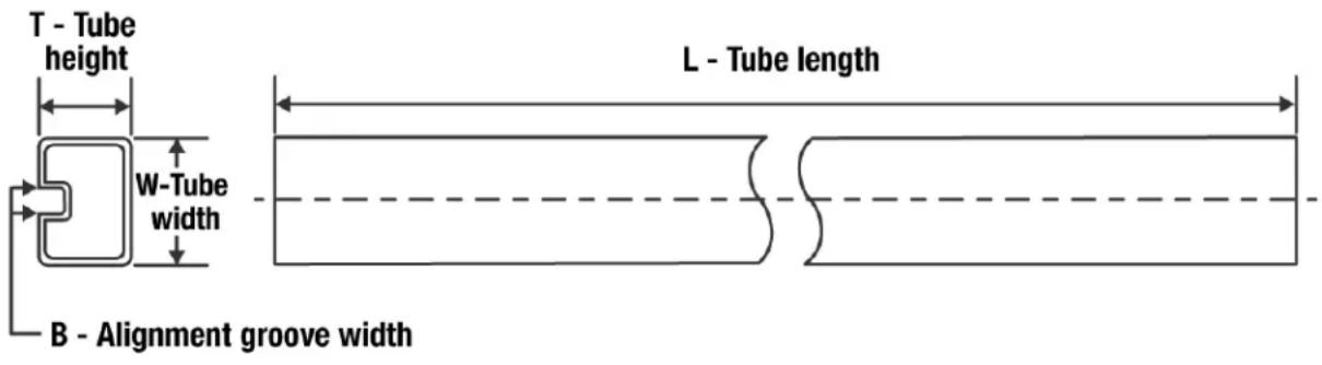
text_image
T - Tube height W-Tube width L - Tube length B - Alignment groove width*All dimensions are nominal
| Device | Package Name | Package Type | Pins | SPQ | L (mm) | W (mm) | T (μm) | B (mm) |
| SN74LVTH16501DL DL | SSOP 56 20 473.7 | 14.24 5110 7.87 | ||||||
| SN74LVTH16501DLG4 DL | SSOP 56 20 473.7 | 14.24 5110 7.87 |
DL (R-PDSO-G56)
PLASTIC SMALL-OUTLINE PACKAGE

text_image
0.025 (0,635) 0.0135 (0,343) 0.008 (0,203) 0.005 (0,13) 56 29 0.420 (10,67) 0.395 (10,03) 0.299 (7,59) 0.291 (7,39) 1 28 0.730 (18,54) 0.720 (18,29) 0.010 (0,25) 0.005 (0,13) Gage Plane 0°-8° 0.010 (0,25) 0.040 (1,02) 0.020 (0,51) Seating Plane 0.110 (2,79) MAX 0.008 (0,20) MIN 4040048-4/F 05/13NOTES: A. All linear dimensions are in inches (millimeters).
B. This drawing is subject to change without notice.
C. Body dimensions do not include mold flash or protrusion not to exceed 0.006 (0,15).
D. Falls within JEDEC MO-118
PowerPAD is a trademark of Texas Instruments.
SMALL OUTLINE PACKAGE

4222167/A 07/2015
NOTES:
- All linear dimensions are in millimeters. Any dimensions in parenthesis are for reference only. Dimensioning and tolerancing per ASME Y14.5M.
- This drawing is subject to change without notice.
- This dimension does not include mold flash, protrusions, or gate burrs. Mold flash, protrusions, or gate burrs shall not exceed 0.15 mm per side.
- Reference JEDEC registration MO-153.
SMALL OUTLINE PACKAGE

text_image
56X (1.5) 1 56X (0.3) 54X (0.5) (R0.05) TYP 28 (7.5) SYMM 56 SYMM 29LAND PATTERN EXAMPLE SCALE:6X
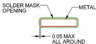
text_image
SOLDER MASK OPENING METAL 0.05 MAX ALL AROUNDNON SOLDER MASK DEFINED

text_image
METAL UNDER SOLDER MASK SOLDER MASK OPENING 0.05 MIN ALL AROUNDSOLDER MASK
DEFINED
SOLDER MASK DETAILS
4222167/A 07/2015
NOTES: (continued)
- Publication IPC-7351 may have alternate designs.
- Solder mask tolerances between and around signal pads can vary based on board fabrication site.
SMALL OUTLINE PACKAGE

text_image
56X (1.5) 1 56X (0.3) 54X (0.5) (R) TYP0.05 28 (7.5) SYMM 56 SYMM 29SOLDER PASTE EXAMPLE BASED ON 0.125 mm THICK STENCIL SCALE:6X
4222167/A 07/2015
NOTES: (continued)
- Laser cutting apertures with trapezoidal walls and rounded corners may offer better paste release. IPC-7525 may have alternate design recommendations.
- Board assembly site may have different recommendations for stencil design.
IMPORTANT NOTICE AND DISCLAIMER
TI PROVIDES TECHNICAL AND RELIABILITY DATA (INCLUDING DATA SHEETS), DESIGN RESOURCES (INCLUDING REFERENCE DESIGNS), APPLICATION OR OTHER DESIGN ADVICE, WEB TOOLS, SAFETY INFORMATION, AND OTHER RESOURCES "AS IS" AND WITH ALL FAULTS, AND DISCLAIMS ALL WARRANTIES, EXPRESS AND IMPLIED, INCLUDING WITHOUT LIMITATION ANY IMPLIED WARRANTIES OF MERCHANTABILITY, FITNESS FOR A PARTICULAR PURPOSE OR NON-INFRINGEMENT OF THIRD PARTY INTELLECTUAL PROPERTY RIGHTS.
These resources are intended for skilled developers designing with TI products. You are solely responsible for (1) selecting the appropriate TI products for your application, (2) designing, validating and testing your application, and (3) ensuring your application meets applicable standards, and any other safety, security, regulatory or other requirements.
These resources are subject to change without notice. TI grants you permission to use these resources only for development of an application that uses the TI products described in the resource. Other reproduction and display of these resources is prohibited. No license is granted to any other TI intellectual property right or to any third party intellectual property right. TI disclaims responsibility for, and you will fully indemnify TI and its representatives against, any claims, damages, costs, losses, and liabilities arising out of your use of these resources.
TI's products are provided subject to TI's Terms of Sale or other applicable terms available either on ti.com or provided in conjunction with such TI products. TI's provision of these resources does not expand or otherwise alter TI's applicable warranties or warranty disclaimers for TI products.
TI objects to and rejects any additional or different terms you may have proposed.
Mailing Address: Texas Instruments, Post Office Box 655303, Dallas, Texas 75265
Copyright © 2022, Texas Instruments Incorporated