CD74HC540E - Electronic component TEXAS INSTRUMENTS - Free user manual and instructions
Find the device manual for free CD74HC540E TEXAS INSTRUMENTS in PDF.

User questions about CD74HC540E TEXAS INSTRUMENTS
0 question about this device. Answer the ones you know or ask your own.
Ask a new question about this device
Download the instructions for your Electronic component in PDF format for free! Find your manual CD74HC540E - TEXAS INSTRUMENTS and take your electronic device back in hand. On this page are published all the documents necessary for the use of your device. CD74HC540E by TEXAS INSTRUMENTS.
USER MANUAL CD74HC540E TEXAS INSTRUMENTS
CDx4HC(T)541 High-Speed CMOS Logic Octal Buffer and Line Drivers, Three-State
1 Features
• 'HC540, CD74HCT540: inverting
• 'HC541, 'HCT541: non-inverting
- Buffered inputs
- Three-state outputs
- Bus line driving capability
• Typical propagation delay = 9 ns at V CC = 5 V, C L = 15 pF, T A = 25°C
• Fanout (over temperature range)
- Standard outputs: 10 LSTTL loads
- Bus driver outputs: 15 LSTTL loads
- Standard outputs: 10 LSTTL loads
- Bus driver outputs: 15 LSTTL loads
- Wide operating temperature range: -55^ to 125^
• Balanced propagation delay and transition times
• Significant power reduction compared to LSTTL Logic ICs
• HC types
- 2 V to 6 V operation
- High noise immunity: NIL = 30% , N_IH = 30% of V_CC at V_CC = 5V
- 2 V to 6 V operation
- High noise immunity: N_IL = 30% , N_IH = 30% of V_CC at V_CC = 5 V
• HCT types
- 4.5 V to 5.5 V operation
- Direct LSTTL input logic compatibility, V_IL = 0.8 ~V (), V_IH = 2 ~V ()
- CMOS input compatibility, I_1 ≤ 1 A at V_OL , V_OH
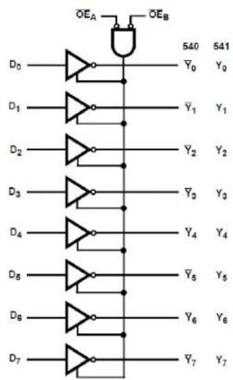
2 Description
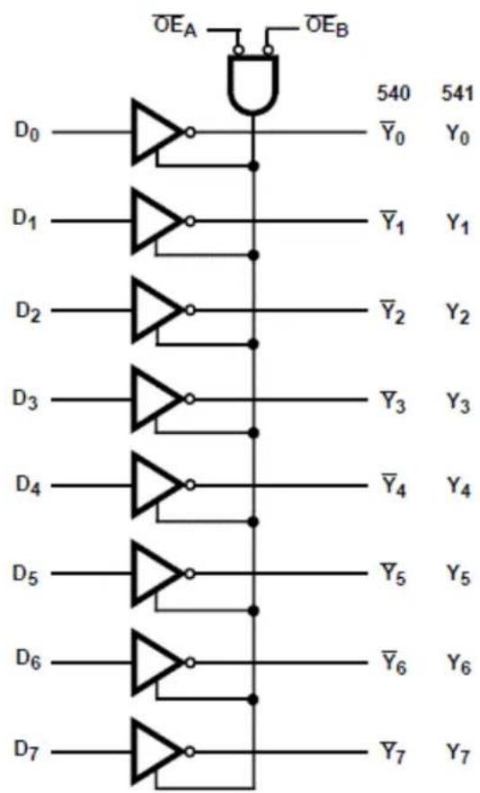
The 'HC540 and CD74HCT540 are Inverting Octal Buffers and Line Drivers with Three-State Outputs and the capability to drive 15 LSTTL loads. The 'HC541 and 'HCT541 are Noninverting Octal Buffers and Line Drivers with Three-State Outputs that can drive 15 LSTTL loads. The Output Enables (OE1) and (OE2) control the Three-State Outputs. If either OE1 or OE2 is HIGH the outputs will be in the high impedance state. For data output OE1 and OE2 both must be LOW.
Device Information
| PART NUMBER PACKAGE (1) | BODY SIZE (NOM) | |
| CD74HC540M SOIC (20) 12.80 mm × | 7.50 mm | |
| CD74HC540E PDIP (20) 25.40 mm × | 6.35 mm | |
| CD54HC540F3A | CDIP (20) | 26.92 mm × 6.92 mm |
| CD74HC541M SOIC (20) 12.80 mm × | 7.50 mm | |
| CD74HC541E PDIP (20) 25.40 mm × | 6.35 mm | |
| CD54HC541F | CDIP (20) | 26.92 mm × 6.92 mm |
| CD74HCT540M SOIC (20) 12.80 mm × | 7.50 mm | |
| CD74HCT540E | PDIP (20) 25.40 mm × | 6.35 mm |
| CD74HCT541M SOIC (20) 12.80 mm × | 7.50 mm | |
| CD74HCT541E | PDIP (20) 25.40 mm × | 6.35 mm |
| CD54HCT541F | CDIP (20) | 26.92 mm × 6.92 mm |
| CD74HCT541PW | TSSOP (20) | 6.50 mm × 4.40 mm |
(1) For all available packages, see the orderable addendum at the end of the data sheet.
flowchart
graph TD
    A["OR Gate"] --> B["D0"]
    A --> C["D1"]
    A --> D["D2"]
    A --> E["D3"]
    A --> F["D4"]
    A --> G["D5"]
    A --> H["D6"]
    A --> I["D7"]
    B --> J["540 Y0"]
    C --> K["541 Y0"]
    D --> L["540 Y1"]
    E --> M["541 Y1"]
    F --> N["540 Y2"]
    G --> O["541 Y2"]
    H --> P["540 Y3"]
    I --> Q["541 Y3"]
    J --> R["540 Y4"]
    K --> S["541 Y4"]
    L --> T["540 Y5"]
    M --> U["541 Y5"]
    N --> V["540 Y6"]
    O --> W["541 Y6"]
    P --> X["540 Y7"]
    Q --> Y["541 Y7"]
    R --> Z["Output 541"]
    S --> AA["Output 541"]
    T --> AB["Output 541"]
    U --> AC["Output 541"]
    V --> AD["Output 541"]
    W --> AE["Output 541"]
    X --> AF["Output 541"]
Functional Diagram

An IMPORTANT NOTICE at the end of this data sheet addresses availability, warranty, changes, use in safety-critical applications, intellectual property matters and other important disclaimers. PRODUCTION DATA.
Table of Contents
1 Features....1
2 Description....1
3 Revision History......2
4 Pin Configuration and Functions....3
5 Specifications....4
5.1 Absolute Maximum Ratings.... 4
5.2 Recommended Operating Conditions......4
5.3 Thermal Information....4
5.4 Electrical Characteristics....5
5.5 Switching Characteristics....6
6 Parameter Measurement Information....8
7 Detailed Description....9
7.1 Overview....9
7.2 Functional Block Diagram....9
7.3 Device Functional Modes....9
8 Power Supply Recommendations....10
9 Layout....10
9.1 Layout Guidelines.... 10
10 Device and Documentation Support....11
10.1 Receiving Notification of Documentation Updates.. 11
10.2 Support Resources.... 11
10.3 Trademarks.... 11
10.4 Electrostatic Discharge Caution.... 11
10.5 Glossary.... 11
11 Mechanical, Packaging, and Orderable Information.... 11
3 Revision History
NOTE: Page numbers for previous revisions may differ from page numbers in the current version.
Changes from Revision C (July 2004) to Revision D (January 2022) Page
- Updated the numbering, formatting, tables, figures, and cross-references throughout the document to reflect modern data sheet standards....1
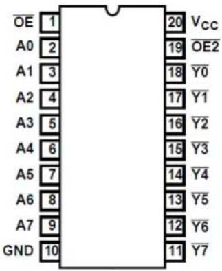
4 Pin Configuration and Functions
text_image
OE 1 A0 2 A1 3 A2 4 A3 5 A4 6 A5 7 A6 8 A7 9 GND 10 20 Vcc 19 OE2 18 Y0 17 Y1 16 Y2 15 Y3 14 Y4 13 Y5 12 Y6 11 Y7HC540
J, N, or DW package
20- Pin CDIP, PDIP, or SOIC
Top View
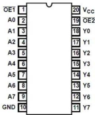
text_image
OE1 1 A0 2 A1 3 A2 4 A3 5 A4 6 A5 7 A6 8 A7 9 GND 10 20 Vcc 19 OE2 18 Y0 17 Y1 16 Y2 15 Y3 14 Y4 13 Y5 12 Y6 11 Y7HC541
J, N, DW, or PW
20-Pin CDIP, PDIP, SOIC, or TSSOP
Top View
5 Specifications
5.1 Absolute Maximum Ratings
over operating free-air temperature range (unless otherwise noted) ^(1)
| MIN MAX UNIT | ||||
| V_CC | Supply voltage -0.5 7 V | |||
| I_IK | Input diode current For V | _1 < -0.5 V or V_I > V_CC + 0.5 V ± 20 mA | ||
| I_OK | Output diode current For V | _O < -0.5 V or V_O > V_CC + 0.5 V ± 20 mA | ||
| I_O | Drain current, per output For -0.5 V < V | _O < V_CC + 0.5 V ± 35 mA | ||
| I_O | Output source or sink current per output pin For V | _O > -0.5 V or V_O < V_CC + 0.5 V ± 25 mA | ||
| Continuous current through V_CC or ground current ±50 mA | ||||
| T_J | Junction temperature 150 °C | |||
| T_stg | Storage temperature range | -65 150 °C | ||
| Lead temperature (Soldering 10s) (SOIC - Lead Tips Only) | 300 °C | |||
(1) Operation outside the Absolute Maximum Ratings may cause permanent device damage. Absolute maximum ratings do not imply functional operation of the device at these or any other conditions beyond those listed under Recommended Operating Conditions. If briefly operating outside the Recommended Operating Conditions but within the Absolute Maximum Ratings, the device may not sustain damage, but it may not be fully functional. Operating the device in this manner may affect device reliability, functionality, performance, and shorten the device lifetime.
5.2 Recommended Operating Conditions
| MIN MAX UNIT | |||||
| T_A | Temperature range | -55 | 125 | °C | |
| V_CC | Supply voltage range | HC types | 2 | 6 | V |
| HCT types | 4.5 | 5.5 | |||
| V_I, V_O | Input or output voltage | 0 | V_CC | V | |
| Input rise and fall time | 2 V | 1000 | ns | ||
| 4.5 V | 500 | ||||
| 6 V | 400 | ||||
5.3 Thermal Information
| THERMAL METRIC | DW (SOIC) | N (PDIP) | PW (TSSOP) | UNIT | |
| 20 PINS | 20 PINS | 20 PINS | |||
| R_ JA | Junction-to-ambient thermal resistance(1) | 58 | 69 | 83 | °C/W |
(1) For more information about traditional and new thermal metrics, see the Semiconductor and IC package thermal metrics application report.
5.4 Electrical Characteristics
| PARAMETER | TEST CONDITIONS(2) | V_CC(V) | 25°C | -40°C to 85°C | -55°C to 125°C | UNIT | |
| MIN TYP MAX MIN MAX | MIN MAX | ||||||
| HC TYPES | |||||||
| V_IH | High level input voltage | 2 1.5 | 1.5 1.5 | V4.5 | |||
| 6 4.2 | 4.2 4.2 | ||||||
| V_IL | Low level input voltage | 2 0.5 | 0.5 0.5 | V4.5 | |||
| 6 1.8 | 1.8 1.8 | ||||||
| V_OH | High level output voltage | I_OH = -20 μA 2 1.9 1.9 1.9 | V | ||||
| CMOS loads | I_OH = -20 μA | 4.5 | 4.4 4.4 4.4 | ||||
| I_OH = -20 μA 6 5.9 5.9 5.9 | |||||||
| High level output voltage | I_OH = -6 mA | 4.5 3.9 | 8 3.84 3.7 | ||||
| TTL loads | I_OH = -7.8 mA | 6 | 5.48 5.34 5.2 | ||||
| V_OL | Low level output voltage | I_OL = 20 μA | 2 0.1 | 0.1 0.1 | V | ||
| CMOS loads | I_OL = 20 μA | 4.5 | 0.1 | 0.1 0.1 | |||
| I_OL = 20 μA | 6 0.1 | 0.1 0.1 | |||||
| Low level output voltage | I_OL = 6 mA | 4.5 0.2 | 6 0.33 0.4 | ||||
| TTL loads | I_OL = 7.8 mA | 6 | 0.26 | 0.33 0.4 | |||
| I_I | Input leakage current | V_I = V_CC or GND | 6 | ±0.1 | ±1 | ±1 | μA |
| I_CC | Quiescent device current | V_I = V_CC or GND | 6 | 8 | 80 | 160 | μA |
| I_OZ | Three-state leakage current | V_O = V_CC or GND 6 | ±0.5 ±5.0 | ±10 | μA | ||
| HCT TYPES | |||||||
| V_IH | High level input voltage | 4.5 to 5.5 | 2 | 2 | 2 | V | |
| V_IL | Low level input voltage | 4.5 to 5.5 | 0.8 | 0.8 0.8 V | |||
| V_OH | High level output voltage | V_OH = -20 μA | 4.5 | 4.4 4.4 4.4 | V | ||
| CMOS loads | |||||||
| High level output voltage | V_OH = -6 mA | 4.5 3.9 | 8 3.84 3.7 | ||||
| V_OL | Low level output voltage | V_OL = 20 μA | 4.5 | 0.1 | 0.1 0.1 | V | |
| CMOS loads | |||||||
| Low level output voltage | V_OL = 6 mA 4.5 0.26 0.33 0.4 | ||||||
| I_I | Input leakage current | V_I = V_CC and GND | 5.5 | ±0.1 | ±1 | ±1 | μA |
| I_CC | Quiescent device current | V_I = V_CC and GND | 5.5 | 8 | 80 | 160 | μA |
| I_OZ | Three-state leakage current | V_O = V_CC or GND 5.5 ±0.5 ±5.0 | ±10 μA | ||||
| I_CC^(1) | HCT540Additional quiescent device current per input pin | A0 - A7 inputs held at V_CC-2.1 | 4.5 to 5.5 | 100 360 450 | 490 μA | ||
| OE2 input held at V_CC-2.1 | 4.5 to 5.5 | 100 270 337.5 | 367.5 μA | ||||
| OE1 input held at V_CC-2.1 | 4.5 to 5.5 | 100 414 517.5 | 563.5 μA | ||||
| HCT541Additional quiescent device current per input pin | A0 - A7 inputs held at V_CC-2.1 | 4.5 to 5.5 | 100 144 180 | 196 μA | |||
| OE2 input held at V_CC-2.1 | 4.5 to 5.5 | 100 270 337.5 | 367.5 μA | ||||
| OE1 input held at V_CC-2.1 | 4.5 to 5.5 | 100 414 517. | 563.5 μA | ||||
(1) For dual-supply systems theoretical worst case (V = 2.4 V, V_CC = 5.5 V ) specification is 1.8mA.
(2) V_I = V_IH or V_OL , unless otherwise noted.
5.5 Switching Characteristics
| PARAMETER | TEST CONDITIONS | V_CC(V) | 25°C | -40°C to 85°C | -55°C to 125°C | UNIT | |
| MIN TYP MAX MIN MAX | MAX MIN MAX | ||||||
| HC TYPES | |||||||
| t_PLH, t_PHL | Propagation delayData to outputs (540) | C_L=50 pF | 2 110 | 140 | 165 | ns | |
| 4.5 | 22 | 28 | 33 | ||||
| C_L=15 pF | 5 | 9 | ns | ||||
| C_L=50 pF | 6 | 19 | 24 | 28 | |||
| t_PLZ, t_PHZ | Data to outputs (541) | C_L=50 pF | 2 115 | 145 | 175 | ns | |
| 4.5 | 23 | 29 | 35 | ||||
| C_L=15 pF | 5 | 9 | ns | ||||
| C_L=50 pF | 6 | 20 | 25 | 30 | |||
| t_PLZ, t_PHZ | Output enable and disable to outputs (540) | C_L=50 pF | 2 | 160 | 200 | 240 | ns |
| 4.5 | 32 | 40 | 48 | ||||
| C_L=15 pF | 5 | 13 | ns | ||||
| C_L=50 pF | 6 | 27 | 34 | 41 | |||
| t_PLZ, t_PHZ | Output enable and disable to outputs (541) | C_L=50 pF | 2 | 160 | 200 | 240 | ns |
| 4.5 | 32 | 40 | 48 | ||||
| C_L=15 pF | 5 | 14 | ns | ||||
| C_L=50 pF | 6 | 23 | 29 | 35 | |||
| t_THL, t_TLH | Output transition time | C_L=50 pF | 2 | 60 | 75 | 90 | ns |
| 4.5 | 12 | 15 | 18 | ||||
| 6 | 10 | 13 | 15 | ||||
| C_I | Input capacitance | C_L=50 pF | 10 10 | 10 | 10 | pF | |
| C_O | Three-state output capacitance | 20 20 | 20 | 20 | pF | ||
| C_PD | Power dissipation capacitance ^(1)(2) (540) | C_L=15 pF | 5 | 50 | pF | ||
| C_PD | Power dissipation capacitance ^(1)(2) (541) | C_L=15 pF | 5 | 48 | pF | ||
| HCT TYPES | |||||||
| t_PHL, t_PLH | Propagation delayData to outputs (540) | C_L=50 pF | 4.5 | 24 | 30 | 36 | ns |
| C_L=15 pF | 5 | 9 | |||||
| t_PHL, t_PLH | Data to outputs (541) | C_L = 50 pF 4.5 | 28 35 42 | ns | |||
| C_L = 15 pF 5 | 11 | ||||||
| t_PLZ, t_PHZ | Output enable and disable to outputs (540, 541) | C_L = 50 pF 4.5 | 35 44 53 | ns | |||
| C_L = 15 pF 5 | 14 | ||||||
| t_TLH, t_THL | Output transition time C | L = 50 pF 4.5 | 12 15 18 ns | ||||
| C_I | Input capacitance C | L = 50 pF 10 | 10 10 10 pF | ||||
| C_O | Three-state output capacitance | 20 20 20 20 pF | |||||
| C_PD | Power dissipation capacitance^(1) (2)(540, 541) | C_L = 15 pF 5 | 55 | pF | |||
(1) C _PD is used to determine the dynamic power consumption, per channel.
(2) P_D = V_CC i(CPD + C_L) where f_i = input frequency, C_L = output load capacitance, V_CC = supply voltage.
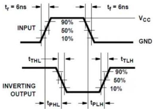
6 Parameter Measurement Information
t_pd is the maximum between t_PLH and t_PHL
t_t is the maximum between t_TLH and t_THL
text_image
tr = 6ns INPUT 90% 50% 10% tf = 6ns VCC GND tTHL INVERTING OUTPUT tPHL tPLH tTLHFigure 6-1. HC Transition Times and Propagation Delay Times, Combination Logic
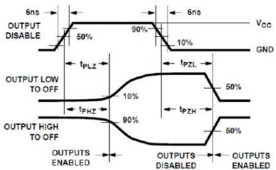
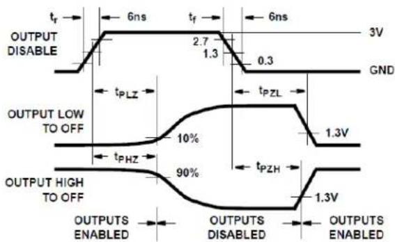
Figure 6-3. HC Three-State Propagation Delay Waveform
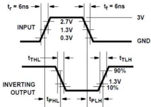
Figure 6-2. HCT Transition Times and Propagation Delay Times, combination Logic
other
| Output Level | Time (ns) | Voltage (V) | | ------------ | --------- | ----------- | | OUTPUT DISABLE | 6 ns | 3 V | | OUTPUT LOW TO OFF | 10% | 1.3 V | | OUTPUT HIGH TO OFF | 90% | 1.3 V |Figure 6-4. HCT Three-State Propagation Delay Waveform

text_image
OTHER INPUTS TIED HIGH OR LOW OUTPUT DISABLE IC WITH THREE- STATE OUTPUT OUTPUT RL = 1kΩ CL 50pF VCC FOR tPLZ AND tPZL GND FOR tPHZ AND tPZHA. Open drain waveforms t PLZ and tPZL are the same as those for three-state shown on the left. The test circuit is Output R_L = 1k to V_CC, C_L = 50 pF .
Figure 6-5. HC and HCT Three-State Propagation Delay Test Circuit
7 Detailed Description
7.1 Overview
The 'HC540 and CD74HCT540 are Inverting Octal Buffers and Line Drivers with Three-State Outputs and the capability to drive 15 LSTTL loads. The 'HC541 and 'HCT541 are Noninverting Octal Buffers and Line Drivers with Three-State Outputs that can drive 15 LSTTL loads. The Output Enables (OE1) and (OE2) control the Three-State Outputs. If either OE1 or OE2 is HIGH the outputs will be in the high impedance state. For data output OE1 and OE2 both must be LOW.
7.2 Functional Block Diagram
flowchart
graph TD
    A["OR Gate"] --> B["D0"]
    A --> C["D1"]
    A --> D["D2"]
    A --> E["D3"]
    A --> F["D4"]
    A --> G["D5"]
    A --> H["D6"]
    A --> I["D7"]
    B --> J["540 Y0"]
    C --> K["541 Y0"]
    D --> L["540 Y1"]
    E --> M["541 Y1"]
    F --> N["540 Y2"]
    G --> O["541 Y2"]
    H --> P["540 Y3"]
    I --> Q["541 Y3"]
    J --> R["540 Y4"]
    K --> S["541 Y4"]
    L --> T["540 Y5"]
    M --> U["541 Y5"]
    N --> V["540 Y6"]
    O --> W["541 Y6"]
    P --> X["540 Y7"]
    Q --> Y["541 Y7"]
    R --> Z["Output 540"]
    S --> AA["Output 541"]
    T --> AB["Output 540"]
    U --> AC["Output 541"]
    V --> AD["Output 540"]
    W --> AE["Output 541"]
7.3 Device Functional Modes
Table 7-1. Truth Table ^(1)
| INPUTS OUTPUTS | ||||
| OE1 OE2 | An 540 541 | |||
| LLHL | H | |||
| HXXZ | Z | |||
| XHXZ | Z | |||
| LLLHL | ||||
(1) H = high voltage level, L = low voltage level, X = don't care, Z = high impedance
8 Power Supply Recommendations
The power supply can be any voltage between the minimum and maximum supply voltage rating located in the Recommended Operating Conditions. Each V_CC terminal should have a good bypass capacitor to prevent power disturbance. A 0.1- F capacitor is recommended for this device. It is acceptable to parallel multiple bypass caps to reject different frequencies of noise. The 0.1- F and 1- F capacitors are commonly used in parallel. The bypass capacitor should be installed as close to the power terminal as possible for best results.
9 Layout
9.1 Layout Guidelines
When using multiple-input and multiple-channel logic devices inputs must not ever be left floating. In many cases, functions or parts of functions of digital logic devices are unused; for example, when only two inputs of a triple-input AND gate are used or only 3 of the 4 buffer gates are used. Such unused input pins must not be left unconnected because the undefined voltages at the outside connections result in undefined operational states. All unused inputs of digital logic devices must be connected to a logic high or logic low voltage, as defined by the input voltage specifications, to prevent them from floating. The logic level that must be applied to any particular unused input depends on the function of the device. Generally, the inputs are tied to GND or V CC, whichever makes more sense for the logic function or is more convenient.
10 Device and Documentation Support
TI offers an extensive line of development tools. Tools and software to evaluate the performance of the device, generate code, and develop solutions are listed below.
10.1 Receiving Notification of Documentation Updates
To receive notification of documentation updates, navigate to the device product folder on ti.com. Click on Subscribe to updates to register and receive a weekly digest of any product information that has changed. For change details, review the revision history included in any revised document.
10.2 Support Resources
TI E2E™ support forums are an engineer's go-to source for fast, verified answers and design help — straight from the experts. Search existing answers or ask your own question to get the quick design help you need.
Linked content is provided "AS IS" by the respective contributors. They do not constitute TI specifications and do not necessarily reflect TI's views; see TI's Terms of Use.
10.3 Trademarks
TI E2E ^™ is a trademark of Texas Instruments.
All trademarks are the property of their respective owners.
10.4 Electrostatic Discharge Caution

This integrated circuit can be damaged by ESD. Texas Instruments recommends that all integrated circuits be handled with appropriate precautions. Failure to observe proper handling and installation procedures can cause damage.
ESD damage can range from subtle performance degradation to complete device failure. Precision integrated circuits may be more susceptible to damage because very small parametric changes could cause the device not to meet its published specifications.
10.5 Glossary
TI Glossary This glossary lists and explains terms, acronyms, and definitions.
11 Mechanical, Packaging, and Orderable Information
The following pages include mechanical, packaging, and orderable information. This information is the most current data available for the designated devices. This data is subject to change without notice and revision of this document. For browser-based versions of this data sheet, refer to the left-hand navigation.
PACKAGING INFORMATION
| Orderable Device Status(1) | Package Type | Package Drawing | Pins | Package Qty | Eco Plan(2) | Lead finish/ Ball material(6) | MSL Peak Temp(3) | Op Temp (°C) | Device Marking(4-5) | Samples | |
| CD54HC540F3A ACTIVE CDIP J 20 1 Non-RoHS | & Green | SNPB N / A for Pkg Type -55 to 125 CD54HC540F3A | Samples | ||||||||
| CD54HC541F ACTIVE CDIP J 20 1 Non-RoHS | & Green | SNPB N / A for Pkg Type -55 to 125 CD54HC541F | Samples | ||||||||
| CD54HC541F3A ACTIVE CDIP J 20 1 Non-RoHS | & Green | SNPB N / A for Pkg Type -55 to 125 CD54HC541F3A | Samples | ||||||||
| CD54HCT541F ACTIVE CDIP J 20 1 Non-RoHS | & Green | SNPB N / A for Pkg Type -55 to 125 CD54HCT541F | Samples | ||||||||
| CD54HCT541F3A ACTIVE CDIP J 20 1 Non-RoHS | & Green | SNPB N / A for Pkg Type -55 to 125 CD54HCT541F3A | Samples | ||||||||
| CD74HC540E ACTIVE PDIP N 20 20 RoHS & | Non-Green | NIPDAU | N / A for Pkg Type -55 to 125 CD74HC540E | Samples | |||||||
| CD74HC540M | ACTIVE | SOIC | DW | 20 | 25 | RoHS & Green | NIPDAU | Level-1-260C-UNLIM | -55 to 125 | HC540M | Samples |
| CD74HC540M96 | ACTIVE | SOIC | DW | 20 | 2000 | RoHS & Green | NIPDAU | Level-1-260C-UNLIM | -55 to 125 | HC540M | Samples |
| CD74HC541E | ACTIVE | PDIP | N | 20 | 20 | RoHS & Green | NIPDAU | N / A for Pkg Type | -55 to 125 | CD74HC541E | Samples |
| CD74HC541EE4 | ACTIVE | PDIP | N | 20 | 20 | RoHS & Green | NIPDAU | N / A for Pkg Type | -55 to 125 | CD74HC541E | Samples |
| CD74HC541M | ACTIVE | SOIC | DW | 20 | 25 | RoHS & Green | NIPDAU | Level-1-260C-UNLIM | -55 to 125 | HC541M | Samples |
| CD74HC541M96 | ACTIVE | SOIC | DW | 20 | 2000 | RoHS & Green | NIPDAU | Level-1-260C-UNLIM | -55 to 125 | HC541M | Samples |
| CD74HC541M96G4 | ACTIVE | SOIC | DW | 20 | 2000 | RoHS & Green | NIPDAU | Level-1-260C-UNLIM | -55 to 125 | HC541M | Samples |
| CD74HC541PW | ACTIVE | TSSOP | PW | 20 | 70 | RoHS & Green | NIPDAU | Level-1-260C-UNLIM | -55 to 125 | HJ541 | Samples |
| CD74HC541PWR | ACTIVE | TSSOP | PW | 20 | 2000 | RoHS & Green | NIPDAU | Level-1-260C-UNLIM | -55 to 125 | HJ541 | Samples |
| CD74HCT540E ACTIVE PDIP N 20 20 RoHS & | Non-Green | NIPDAU | N / A for Pkg Type -55 to 125 CD74HCT540E | Samples | |||||||
| CD74HCT540M | ACTIVE | SOIC | DW | 20 | 25 | RoHS & Green | NIPDAU | Level-1-260C-UNLIM | -55 to 125 | HCT540M | Samples |
| CD74HCT540M96 | ACTIVE | SOIC | DW | 20 | 2000 | RoHS & Green | NIPDAU | Level-1-260C-UNLIM | -55 to 125 | HCT540M | Samples |
| Orderable Device Status(1) | Package Type | Package Drawing | Pins | Package Qty | Eco Plan(2) | Lead finish/ Ball material(6) | MSL Peak Temp(3) | Op Temp (°C) | Device Marking(4/5) | Samples | |
| CD74HCT541E | ACTIVE | PDIP N 20 | RoHS & | Non-Green | NIPDAU N / A for Pkg Type -55 to 125 CD74HCT541E | Samples | |||||
| CD74HCT541M | ACTIVE | SOIC | DW | 20 | 25 | RoHS & Green | NIPDAU | Level-1-260C-UNLIM | -55 to 125 | HCT541M | Samples |
| CD74HCT541M96 | ACTIVE | SOIC | DW | 20 | 2000 | RoHS & Green | NIPDAU | Level-1-260C-UNLIM | -55 to 125 | HCT541M | Samples |
| CD74HCT541M96E4 | ACTIVE | SOIC | DW | 20 | 2000 | RoHS & Green | NIPDAU | Level-1-260C-UNLIM | -55 to 125 | HCT541M | Samples |
| CD74HCT541M96G4 | ACTIVE | SOIC | DW | 20 | 2000 | RoHS & Green | NIPDAU | Level-1-260C-UNLIM | -55 to 125 | HCT541M | Samples |
(1) The marketing status values are defined as follows:
ACTIVE: Product device recommended for new designs.
LIFEBUY: TI has announced that the device will be discontinued, and a lifetime-buy period is in effect.
NRND: Not recommended for new designs. Device is in production to support existing customers, but TI does not recommend using this part in a new design.
PREVIEW: Device has been announced but is not in production. Samples may or may not be available.
OBSOLETE: TI has discontinued the production of the device.
(2) RoHS: TI defines "RoHS" to mean semiconductor products that are compliant with the current EU RoHS requirements for all 10 RoHS substances, including the requirement that RoHS substance do not exceed 0.1% by weight in homogeneous materials. Where designed to be soldered at high temperatures, "RoHS" products are suitable for use in specified lead-free processes. TI may reference these types of products as "Pb-Free".
RoHS Exempt: TI defines "RoHS Exempt" to mean products that contain lead but are compliant with EU RoHS pursuant to a specific EU RoHS exemption.
Green: TI defines "Green" to mean the content of Chlorine (Cl) and Bromine (Br) based flame retardants meet JS709B low halogen requirements of <=1000ppm threshold. Antimony trioxide based flame retardants must also meet the <=1000ppm threshold requirement.
(3) MSL, Peak Temp. - The Moisture Sensitivity Level rating according to the JEDEC industry standard classifications, and peak solder temperature.
(4) There may be additional marking, which relates to the logo, the lot trace code information, or the environmental category on the device.
(5) Multiple Device Markings will be inside parentheses. Only one Device Marking contained in parentheses and separated by a "\~" will appear on a device. If a line is indented then it is a continuation of the previous line and the two combined represent the entire Device Marking for that device.
(6) Lead finish/Ball material - Orderable Devices may have multiple material finish options. Finish options are separated by a vertical ruled line. Lead finish/Ball material values may wrap to two lines if the finish value exceeds the maximum column width.
Important Information and Disclaimer: The information provided on this page represents TI's knowledge and belief as of the date that it is provided. TI bases its knowledge and belief on information provided by third parties, and makes no representation or warranty as to the accuracy of such information. Efforts are underway to better integrate information from third parties. TI has taken and
continues to take reasonable steps to provide representative and accurate information but may not have conducted destructive testing or chemical analysis on incoming materials and chemicals. TI and TI suppliers consider certain information to be proprietary, and thus CAS numbers and other limited information may not be available for release.
In no event shall TI's liability arising out of such information exceed the total purchase price of the TI part(s) at issue in this document sold by TI to Customer on an annual basis.
OTHER QUALIFIED VERSIONS OF CD54HC540, CD54HC541, CD54HCT541, CD74HC540, CD74HC541, CD74HCT541 :
• Catalog : CD74HC540, CD74HC541, CD74HCT541
• Military : CD54HC540, CD54HC541, CD54HCT541
NOTE: Qualified Version Definitions:
• Catalog - TI's standard catalog product
• Military - QML certified for Military and Defense Applications
TAPE AND REEL INFORMATION
*All dimensions are nominal
| Device Package | Type | Package Drawing | Pins | SPQ Reel | Diameter (mm) | Reel Width W1 (mm) | A0 (mm) | B0 (mm) | K0 (mm) | P1 (mm) | W (mm) | Pin1 Quadrant |
| CD74HC540M96 SOIC | DW 20 | 2000 330.0 | 24.4 | 10.8 13.3 | 2.7 12.0 24 | 0 Q1 | ||||||
| CD74HC541M96 SOIC | DW 20 | 2000 330.0 | 24.4 | 10.8 13.3 | 2.7 12.0 24 | 0 Q1 | ||||||
| CD74HC541PWR TSS | OP PW 20 | 2000 330.0 | 16. | 4 6.95 7.1 | 1.6 8.0 16 | 0 Q1 | ||||||
| CD74HCT540M96 SOIC | DW 20 | 2000 330.0 | 24.4 | 10.8 13.3 | 2.7 12.0 24 | 0 Q1 | ||||||
| CD74HCT541M96 SOIC | DW 20 | 2000 330.0 | 24.4 | 10.8 13.3 | 2.7 12.0 24 | 0 Q1 |
text_image
TAPE AND REEL BOX DIMENSIONS W L*All dimensions are nominal
| Device | Package Type | Package Drawing | Pins | SPQ | Length (mm) | Width (mm) | Height (mm) |
| CD74HC540M96 SOIC | DW 20 2000 367.0 | 367.0 45.0 | |||||
| CD74HC541M96 SOIC | DW 20 2000 367.0 | 367.0 45.0 | |||||
| CD74HC541PWR TSSOP | PW 20 2000 853.0 | 449.0 35.0 | |||||
| CD74HCT540M96 SOIC | DW 20 2000 367.0 | 367.0 45.0 | |||||
| CD74HCT541M96 SOIC | DW 20 2000 367.0 | 367.0 45.0 |
TUBE

text_image
T - Tube height L - Tube length W-Tube width B - Alignment groove width*All dimensions are nominal
| Device | Package Name | Package Type | Pins | SPQ | L (mm) | W (mm) | T (μm) | B (mm) |
| CD74HC540E N PDIP | 20 20 506 13.97 1 | 1230 4.32 | ||||||
| CD74HC540M DW SOIC | 20 25 507 12.8 | 5080 | 6.6 | |||||
| CD74HC541E N PDIP | 20 20 506 13.97 1 | 1230 4.32 | ||||||
| CD74HC541EE4 | N PDIP 20 | 20 506 13.97 1 | 230 4.32 | |||||
| CD74HC541M DW SOIC | 20 25 507 12.8 | 5080 | 6.6 | |||||
| CD74HC541PW | PW | TSSOP | 20 | 70 | 530 | 10.2 | 3600 | 3.5 |
| CD74HCT540E | N PDIP 20 | 20 506 13.97 1 | 230 4.32 | |||||
| CD74HCT540M | DW | SOIC | 20 | 25 | 507 | 12.83 | 5080 | 6.6 |
| CD74HCT541E | N PDIP 20 | 20 506 13.97 1 | 230 4.32 | |||||
| CD74HCT541M | DW | SOIC | 20 | 25 | 507 | 12.83 | 5080 | 6.6 |
text_image
B 14 8 C 1 0.065 (1,65) 0.045 (1,14)| PINS **DIM | 14 | 16 | 18 | 20 |
| A | 0.300(7,62)BSC | 0.300(7,62)BSC | 0.300(7,62)BSC | 0.300(7,62)BSC |
| B MAX | 0.785(19,94) | .840(21,34) | 0.960(24,38) | 1.060(26,92) |
| B MIN | — | — | — | — |
| C MAX | 0.300(7,62) | 0.300(7,62) | 0.310(7,87) | 0.300(7,62) |
| C MIN | 0.245(6,22) | 0.245(6,22) | 0.220(5,59) | 0.245(6,22) |

text_image
0.005 (0,13) MIN 0.060 (1,52) 0.015 (0,38) 0.200 (5,08) MAX Seating Plane 0.130 (3,30) MIN 0.026 (0,66) 0.014 (0,36) 0.100 (2,54) 0.014 (0,36) 0.008 (0,20) A 0°-15°4040083/F 03/03
NOTES:
A. All linear dimensions are in inches (millimeters).
B. This drawing is subject to change without notice.
C. This package is hermetically sealed with a ceramic lid using glass frit.
D. Index point is provided on cap for terminal identification only on press ceramic glass frit seal only.
E. Falls within MIL STD 1835 GDIP1-T14, GDIP1-T16, GDIP1-T18 and GDIP1-T20.
N (R-PDIP-T\*\*)
16 PINS SHOWN
PLASTIC DUAL-IN-LINE PACKAGE

text_image
A 16 9 0.260 (6,60) 0.240 (6,10) 1 8 0.070 (1,78) 0.045 (1,14)C
| DIM\PINS ** | 14 | 16 | 18 | 20 |
| A MAX | 0.775(19,69) | 0.775(19,69) | 0.920(23,37) | 1.060(26,92) |
| A MIN | 0.745(18,92) | 0.745(18,92) | 0.850(21,59) | 0.940(23,88) |
| MS-001VARIATION | AA | BB | AC | AD |
text_image
0.045 (1,14) 0.030 (0,76) D 0.020 (0,51) MIN 0.200 (5,08) MAX Seating Plane 0.125 (3,18) MIN 0.100 (2,54) 0.021 (0,53) 0.015 (0,38) ⊕ 0.010 (0,25) M 14/18 Pin Only 20 Pin vendor opt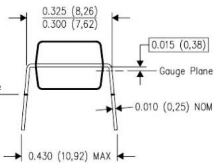
text_image
0.325 (8,26) 0.300 (7,62) 0.015 (0,38) Gauge Plane 0.010 (0,25) NOM 0.430 (10,92) MAX4040049/E 12/2002
NOTES: A. All linear dimensions are in inches (millimeters).
B. This drawing is subject to change without notice.
C Falls within JEDEC MS-001, except 18 and 20 pin minimum body length (Dim A).
The 20 pin end lead shoulder width is a vendor option, either half or full width.
SOIC

4220724/A 05/2016
NOTES:
- All linear dimensions are in millimeters. Dimensions in parenthesis are for reference only. Dimensioning and tolerancing per ASME Y14.5M.
- This drawing is subject to change without notice.
- This dimension does not include mold flash, protrusions, or gate burrs. Mold flash, protrusions, or gate burrs shall not exceed 0.15 mm per side.
- This dimension does not include interlead flash. Interlead flash shall not exceed 0.43 mm per side.
- Reference JEDEC registration MS-013.
SOIC
text_image
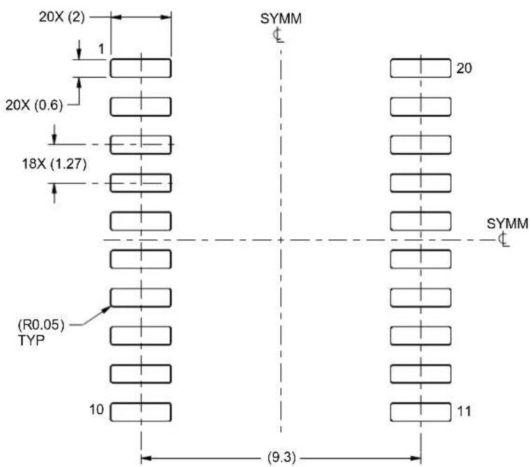
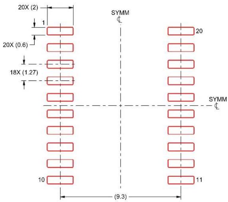
20X (2) 1 20X (0.6) 18X (1.27) (R0.05) TYP 10 SYMM 20 SYMM 11 (9.3)LAND PATTERN EXAMPLE SCALE:6X
text_image
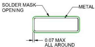
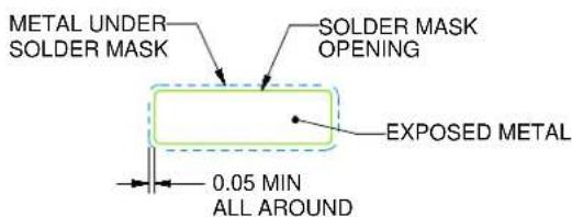
SOLDER MASK OPENING METAL 0.07 MAX ALL AROUNDNON SOLDER MASK DEFINED
text_image
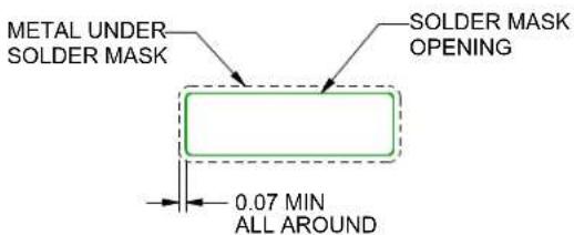
METAL UNDER SOLDER MASK SOLDER MASK OPENING 0.07 MIN ALL AROUNDSOLDER MASK
DEFINED
SOLDER MASK DETAILS
4220724/A 05/2016
NOTES: (continued)
- Publication IPC-7351 may have alternate designs.
- Solder mask tolerances between and around signal pads can vary based on board fabrication site.
SOIC
text_image
20X (2) 1 20X (0.6) 18X (1.27) SYMM 20 SYMM 10 (9.3) 11SOLDER PASTE EXAMPLE
BASED ON 0.125 mm THICK STENCIL
SCALE:6X
4220724/A 05/2016
NOTES: (continued)
- Laser cutting apertures with trapezoidal walls and rounded corners may offer better paste release. IPC-7525 may have alternate design recommendations.
- Board assembly site may have different recommendations for stencil design.
SMALL OUTLINE PACKAGE

text_image
A 6.6 TYP 6.2 PIN 1 INDEX AREA 1 20 18X 0.65 6.6 6.4 NOTE 3 2X 5.85 10 11 20X 0.30 0.19 B 4.5 4.3 NOTE 4 ⊕ 0.1@ A B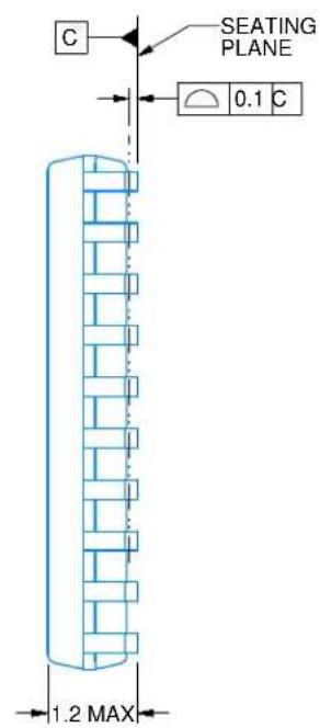
text_image
C SEATING PLANE 0.1 C 1.2 MAX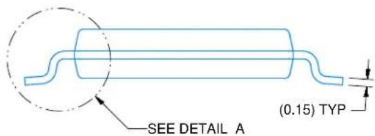
text_image
SEE DETAIL A (0.15) TYP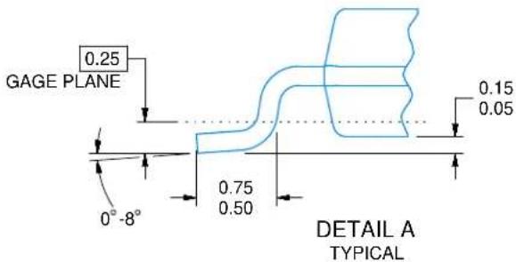
text_image
GAGE PLANE 0.25 0.15 0.05 0° -8° 0.75 0.50 DETAIL A TYPICAL4220206/A 02/2017
NOTES:
- All linear dimensions are in millimeters. Any dimensions in parenthesis are for reference only. Dimensioning and tolerancing per ASME Y14.5M.
- This drawing is subject to change without notice.
- This dimension does not include mold flash, protrusions, or gate burrs. Mold flash, protrusions, or gate burrs shall not exceed 0.15 mm per side.
- This dimension does not include interlead flash. Interlead flash shall not exceed 0.25 mm per side.
- Reference JEDEC registration MO-153.
SMALL OUTLINE PACKAGE
text_image
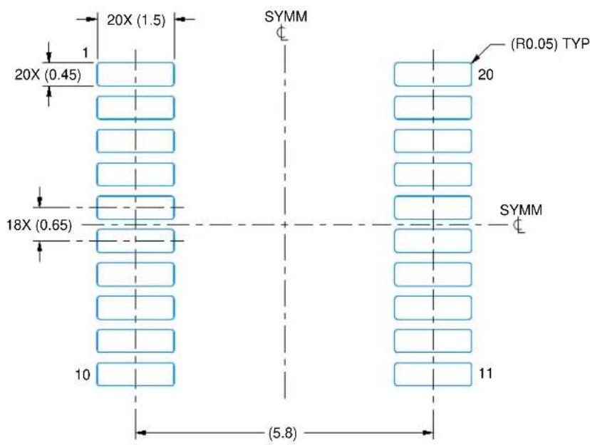
20X (1.5) 1 20X (0.45) SYMM (R0.05) TYP 18X (0.65) 10 (5.8) 11 SYMMLAND PATTERN EXAMPLE
EXPOSED METAL SHOWN
SCALE: 10X

text_image
SOLDER MASK OPENING METAL EXPOSED METAL 0.05 MAX ALL AROUNDNON-SOLDER MASK DEFINED (PREFERRED)
text_image
METAL UNDER SOLDER MASK SOLDER MASK OPENING EXPOSED METAL 0.05 MIN ALL AROUNDSOLDER MASK DETAILS
4220206/A 02/2017
NOTES: (continued)
- Publication IPC-7351 may have alternate designs.
- Solder mask tolerances between and around signal pads can vary based on board fabrication site.
SMALL OUTLINE PACKAGE
text_image
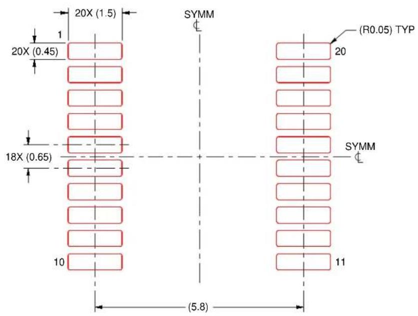
20X (1.5) 1 20X (0.45) 18X (0.65) 10 (5.8) SYMM (20) (R0.05) TYP SYMM 11SOLDER PASTE EXAMPLE
BASED ON 0.125 mm THICK STENCIL
SCALE: 10X
4220206/A 02/2017
NOTES: (continued)
- Laser cutting apertures with trapezoidal walls and rounded corners may offer better paste release. IPC-7525 may have alternate design recommendations.
- Board assembly site may have different recommendations for stencil design.
PW (R-PDSO-G20)
Example Board Layout
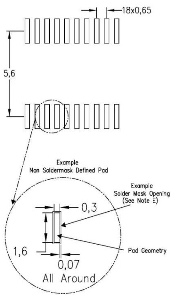
text_image
18x0,65 5,6 Example Non Soldermask Defined Pad Example Solder Mask Opening (See Note E) 0,3 1,6 0,07 Pad Geometry All AroundBased on a stencil thickness of .127mm (.005inch).
text_image
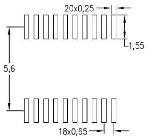
20x0,25 1,55 5,6 18x0,654211284-5/G 08/15
NOTES:
A. All linear dimensions are in millimeters.
B. This drawing is subject to change without notice.
C. Publication IPC-7351 is recommended for alternate design.
D. Laser cutting apertures with trapezoidal walls and also rounding corners will offer better paste release. Customers should contact their board assembly site for stencil design recommendations. Refer to IPC-7525 for other stencil recommendations.
E. Customers should contact their board fabrication site for solder mask tolerances between and around signal pads.
IMPORTANT NOTICE AND DISCLAIMER
TI PROVIDES TECHNICAL AND RELIABILITY DATA (INCLUDING DATA SHEETS), DESIGN RESOURCES (INCLUDING REFERENCE DESIGNS), APPLICATION OR OTHER DESIGN ADVICE, WEB TOOLS, SAFETY INFORMATION, AND OTHER RESOURCES "AS IS" AND WITH ALL FAULTS, AND DISCLAIMS ALL WARRANTIES, EXPRESS AND IMPLIED, INCLUDING WITHOUT LIMITATION ANY IMPLIED WARRANTIES OF MERCHANTABILITY, FITNESS FOR A PARTICULAR PURPOSE OR NON-INFRINGEMENT OF THIRD PARTY INTELLECTUAL PROPERTY RIGHTS.
These resources are intended for skilled developers designing with TI products. You are solely responsible for (1) selecting the appropriate TI products for your application, (2) designing, validating and testing your application, and (3) ensuring your application meets applicable standards, and any other safety, security, regulatory or other requirements.
These resources are subject to change without notice. TI grants you permission to use these resources only for development of an application that uses the TI products described in the resource. Other reproduction and display of these resources is prohibited. No license is granted to any other TI intellectual property right or to any third party intellectual property right. TI disclaims responsibility for, and you will fully indemnify TI and its representatives against, any claims, damages, costs, losses, and liabilities arising out of your use of these resources.
TI's products are provided subject to TI's Terms of Sale or other applicable terms available either on ti.com or provided in conjunction with such TI products. TI's provision of these resources does not expand or otherwise alter TI's applicable warranties or warranty disclaimers for TI products.
TI objects to and rejects any additional or different terms you may have proposed.
Mailing Address: Texas Instruments, Post Office Box 655303, Dallas, Texas 75265
Copyright © 2022, Texas Instruments Incorporated