SN74AVC16T245DGVR - Electronic component TEXAS INSTRUMENTS - Free user manual and instructions
Find the device manual for free SN74AVC16T245DGVR TEXAS INSTRUMENTS in PDF.

User questions about SN74AVC16T245DGVR TEXAS INSTRUMENTS
0 question about this device. Answer the ones you know or ask your own.
Ask a new question about this device
Download the instructions for your Electronic component in PDF format for free! Find your manual SN74AVC16T245DGVR - TEXAS INSTRUMENTS and take your electronic device back in hand. On this page are published all the documents necessary for the use of your device. SN74AVC16T245DGVR by TEXAS INSTRUMENTS.
USER MANUAL SN74AVC16T245DGVR TEXAS INSTRUMENTS
SN74AVC16T24516-BitDual-SupplyBusTransceiver
withConfigurableLevel-Shifting/VoltageTranslationandTri-StateOutputs
1Features3Description
•ControlInputsV IH/VIL LevelsAreReferencedto V_CCA Voltage
- V_CC IsolationFeature—IfEitherV CC InputIsat GND, BothPortsAreintheHigh-ImpedanceState
•Overvoltage-TolerantInputsandOutputsAllow Mixed-Voltage-ModeDataCommunications
- FullyConfigurableDual-RailDesignAllowsEach PorttoOperateOvertheFull1.2Vto3.6V Power-SupplyRange
- Ioff SupportsPartial-Power-DownModeOperation
• I/OsAre4.6VTolerant
•MaximumDataRates
- 380Mbps(1.8Vto3.3VLevel-Shifting)
- 200Mbps(<1.8Vto3.3VLevel-Shifting)
- 200Mbps(Level-Shiftingto2.5Vor1.8V)
- 150Mbps(Level-Shiftingto1.5V)
-
100Mbps(Level-Shiftingto1.2V)
-
Latch-UpPerformanceExceeds100mAPer JESD78,ClassII
•ESDProtectionExceedsJESD22 -
8000-VHuman-BodyModel(A114-A)
- 200-VMachineModel(A115-A)
- 1000-VCharged-DeviceModel(C101)
2Applications
•PersonalElectronics
- Industrial
- Enterprise
•Telecom
This16-bitnoninvertingbustransceiverusestwo separateconfigurablepower-supplyrails. The SN74AVC16T245deviceisoptimizedtooperatewith V_CCA/V_CCB setat1.4 Vto3.6 V. Thedevice is operationalwith V_CCA/V_CCB aslowas1.2V. The A port is designed to track V_CCA . V_CCA accepts any supply voltage from 1.2 V to 3.6 V. The B port is designed to track V_CCB . V_CCB accepts any supply voltage from 1.2 V to 3.6 V. This allows for universal low-voltage bidirectional translation between any of the1.2-V,1.5-V,1.8-V,2.5-V,and3.3-Vvoltage nodes.
TheSN74AVC16T245deviceisdesigned for asynchronous communication between data buses. ThedevicetransmitsdatafromtheAbustotheBbusorfromtheBbustotheAbus,dependingonthe logic level at the direction-control (DIR) input. The output-enable (OE) input can be used to disable the outputssothebuseseffectivelyareisolated.
The SN74AVC16T245 control pins (1DIR, 2DIR, 1OE, and 2OE) aresupplied by V CCA.
DeviceInformation ^(1)
| PART NUMBER | PACKAGE | BODY SIZE (NOM) |
| SN74AVC16T245 | TSSOP (48) | 12.50 mm × 6.10 mm |
| TVSOP (48) | 9.70 mm × 4.40 mm | |
| BGA MICROSTAR JUNIOR (56) | 7.00 mm× 4.50 mm |
(1) For all available packages, see the orderable addendum at the end of the data sheet.
LogicDiagram(PositiveLogic)
flowchart
graph TD
    A["1DIR"] --> B["AND"]
    B --> C["48"]
    C --> D["1OE"]
    E["1A1"] --> F["NOT"]
    F --> G["47"]
    G --> H["NOT"]
    H --> I["2"]
    I --> J["1B1"]
    K["Ground"] --> L["Output"]
To Seven Other Channels
flowchart
graph TD
    A["2DIR"] --> B["AND"]
    B --> C["2OE"]
    D["2A1"] --> E["NOT"]
    E --> F["2B1"]
    G["2OE"] --> H["NOT"]
    H --> I["2B1"]
    J["2A1"] --> K["NOT"]
    K --> L["2B1"]
    M["2B1"] --> N["NOT"]
    N --> O["2B1"]
    P["2DIR"] --> Q["24"]
    R["2OE"] --> S["25"]
    T["2A1"] --> U["36"]
    V["2B1"] --> W["13"]
To Seven Other Channels
TableofContents
1 Features.... 1
2 Applications 1
3 Description 1
4 Revision History...... 2
5Description(continued)....3
6PinConfigurationandFunctions....4
7 Specifications....5
7.1 AbsoluteMaximumRatings....5
7.2ESDRatings....5
7.3RecommendedOperatingConditions....6
7.4ThermalInformation....6
7.5 Electrical Characteristics....7
7.6SwitchingCharacteristics:V CCA =1.2V....8
7.7SwitchingCharacteristics:V CCA=1.5V±0.1V.....8
7.8SwitchingCharacteristics:V _CCA=1.8V±0.15V8
7.9SwitchingCharacteristics:V CCA=2.5V±0.2V.....9
7.10SwitchingCharacteristics:V CCA =3.3V±0.3V.....9
7.11 OperatingCharacteristics....9
7.12TypicalCharacteristics....10
8ParameterMeasurementInformation....12
9 Detailed Description 13
9.1Overview....13
9.2FunctionalBlockDiagram....13
9.3FeatureDescription....13
9.4DeviceFunctionalModes....14
10ApplicationandImplementation....15
10.1 Application Information....15
10.2TypicalApplication....16
11PowerSupplyRecommendations....18
12 Layout.... 18
12.1 LayoutGuidelines....18
12.2LayoutExample....19
13DeviceandDocumentationSupport....20
13.1 DocumentationSupport....20
13.2 Community Resources....20
13.3Trademarks....20
13.4ElectrostaticDischargeCaution....20
13.5Glossary....20
14Mechanical, Packaging, and Orderable Information 20
4RevisionHistory
NOTE: Pagenumbersforpreviousrevisionsmaydifferfrompagenumbersinthecurrentversion.
ChangesfromRevisionD(February2015)toRevisionE
Page
- Updated Pin Functions Table. 4
ChangesfromRevisionC(August2005)toRevisionD
Page
- Added ESD Ratings table, Feature Description section, Device Functional Modes, Application and Implementation section, Power Supply Recommendations section, Layout section, Device and Documentation Support section, and Mechanical, Packaging, and Orderable Information section .... 1
5Description(continued)
This device is fully specified for partial-power-down applications using l_off . The l_off circuitry disable the outputs, preventing damaging current back flow through the device when it is powered down.
TheV CC isolationfeatureensuresthatifeitherV CC inputisatGND,bothportsareinthehigh-impedancestate.
Toensurethehigh-impedancestateduringpoweruporpowerdown,OEshouldbetiedtoV CCA throughapullup resistor;theminimumvalueoftheresistorisdeterminedbythecurrent-sinkingcapabilityofthedriver.
6PinConfigurationandFunctions
GQLorZQLPackage
56-PinBGAMICROSTARJUNIOR
TopView
21 3 4 65

text_image
A B C D E F G H J KDGGorDGVPackage
48-PinTSSOPorTVSOP
TopView

text_image
1DIR 1 48 1OE 1B1 2 47 1A1 1B2 3 46 1A2 GND 4 45 GND 1B3 5 44 1A3 1B4 6 43 1A4 VCCB 7 42 VCCA 1B5 8 41 1A5 1B6 9 40 1A6 GND 10 39 GND 1B7 11 38 1A7 1B8 12 37 1A8 2B1 13 36 2A1 2B2 14 35 2A2 GND 15 34 GND 2B3 16 33 2A3 2B4 17 32 2A4 VCCB 18 31 VCCA 2B5 19 30 2A5 2B6 20 29 2A6 GND 21 28 GND 2B7 22 27 2A7 2B8 23 26 2A8 2DIR 24 25 2OEPinFunctions
| PIN | I/ODESCRIPTION | ||
| NAME | TSSOP,BGA TVSOPMICROSTAR | ||
| 1DIR,2DIR1,24A1,K1 | I Direction-controlsignal | ||
| 1B1to1B8 | 2,3,5,6,8,9, B2,11,12 | B1,C2,C1,D2,D1,E2,E1 | I/O Input/Output.ReferencedtoV CCB |
| 2B1to2B8 | 13,14,16,17, 19,20,22,23 | F1,F2,G1,G2,H1,H2,J1,J2 | I/O Input/Output.ReferencedtoV CCB |
| GND | 4,10,15,21, 45,39,34,28 | B3,D3,G3,J3,J4,G4,D4,B4 | — Ground |
| V_CCB | 7, 18 | C3, H3 | — B-port supply voltage. 1.2 V ≤ V_CCB ≤ 3.6 V |
| 1OE,2OE | 48,25A6, K6 | — | |
| 1A1to1A8 | 47,46,44,43, 41,40,38,37 | B5,B6,C5,C6,D5,D6,E5,E6 | I/O Input/Output.ReferencedtoV CCA |
| 2A1to2A8 | 36,35,33,32, 30,29,27,26 | F6,F5,G6,G5,H6,H5,J6,J5 | I/O Input/Output.ReferencedtoV CCA |
| V_CCA | 42, 31 | C4, H4 | — A-port supply voltage. 1.2 V ≤ V_CCB ≤ 3.6 V |
| N.C. | — | A2,A3,A4,A5,K2,K3,K4,K5 | — Nointernalconnection |
7Specifications
7.1 Absolute Maximum Ratings
overoperatingfree-airtemperaturerange(unlessotherwisenoted) (1)
| MINMAXUNIT | ||||
| V_CCA V_CCB Supplyvoltage-0.54.6V | ||||
| V_I Inputvoltage (2) | I/Oports(Aport)-0.54.6 | |||
| I/Oports(Bport)-0.54.6V | ||||
| Controlinputs-0.54.6 | ||||
| V_O Voltagerangeappliedtoanyoutputinthehigh-impedanceorpower-offstate (2) | Aport-0.54.6 | V | ||
| Bport-0.54.6 | ||||
| V_O Voltagerangeappliedtoanyoutputinthehighorlowstate (2)(3) | Aport-0.5 V | CCA+0.5 | V | |
| Bport-0.5 V | CCB+0.5 | |||
| I_IK Inputclampcurrent | V_I<0 | -50 | mA | |
| I_OK Outputclampcurrent | V_O<0 | -50 | mA | |
| I_O Continuousoutputcurrent | ±50 | mA | ||
| ContinuouscurrentthrougheachV CCA , V_CCB ,andGND | ±100 | mA | ||
| R_BJA Packagethermalimpedance (4) | DGGpackage | 70 | °C/W | |
| DGVpackage | 58 | |||
| GQL/ZQLpackage | 42 | |||
| T_J Junctiontemperature | -40150 °C | |||
| T_stg Storagetemperature | -65150 °C | |||
(1) Stresses beyond those listed under Absolute Maximum Ratings may cause permanent damage to the device. These are stress ratings only, which do not imply functional operation of the device at these or any other conditions beyond those indicated under Recommended Operating Conditions. Exposure to absolute-maximum-rated conditions for extended periods may affect device reliability.
(2) The input voltage(V ) and output negative-voltage(V ) ratings may be exceeded if the input and output current ratings are observed.
(3) The output positive-voltage rating may be exceeded up to 4.6 V maximum if the output current rating is observed.
(4) ThepackagethermalimpedanceiscalculatedinaccordancewithJESD51-7.
7.2ESDRatings
| VALUE | UNIT | ||
| V_(ESD) Electrostaticdischarge | Human-bodymodel(HBM),perANSI/ESDA/JEDECJS-001 (1) | ±8000 | V |
| Charged-devicemodel(CDM),perJEDECspecificationJESD22-C101(2) | ±1000 | ||
| Machinemodel(A115-A) | ±200 | ||
(1) JEDEC document JEP155 states that 500-V HBM allows safe manufacturing with a standard ESD control process. Manufacturing with lessthan500-VHBMispossiblewiththenecessaryprecautions.
(2) JEDEC document JEP157 states that 250-V CDM allows safe manufacturing with a standard ESD control process. Manufacturing with lessthan250-VCDMispossiblewiththenecessaryprecautions.
7.3 Recommended Operating Conditions
overoperatingfree-airtemperaturerange(unlessotherwisenoted) (1)(2)(3)
| V_CCI | V_CCO | MINMAXUNIT | ||||
| V_CCA | Supplyvoltage1.23.6V | |||||
| V_CCB | Supplyvoltage1.23.6V | |||||
| V_IH | High-level inputvoltage | Datainputs (4) | 1.2Vto1.95VV | CCI ×0.65 | ||
| 1.95Vto2.7V1.6V | ||||||
| 2.7Vto3.6V2 | ||||||
| V_IL | Low-level inputvoltage | Datainputs (4) | 1.2Vto1.95V | VCCI ×0.35 | ||
| 1.95Vto2.7V | 0.7V | |||||
| 2.7Vto3.6V | 0.8 | |||||
| V_IH | High-level inputvoltage | DIR (referenced to V_CCA)^(5) | 1.2Vto1.95V | VCCA ×0.65 | ||
| 1.95Vto2.7V1.6V | ||||||
| 2.7Vto3.6V2 | ||||||
| V_IL | Low-level inputvoltage | DIR (referenced to V_CCA)^(5) | 1.2Vto1.95V | VCCA ×0.35 | ||
| 1.95Vto2.7V | 0.7V | |||||
| 2.7Vto3.6V | 0.8 | |||||
| V_I | Inputvoltage | 03.6V | ||||
| V_O | Outputvoltage | Activestate | 0 VCCO | V | ||
| Tri-State | 03.6 | |||||
| I_OH | High-level output current | 1.2V | -3 | mA | ||
| 1.4Vto1.6V | -6 | |||||
| 1.65 V to 1.95 V | -8 | |||||
| 2.3Vto2.7V | -9 | |||||
| 3Vto3.6V | -12 | |||||
| I_OL | Low-level output current | 1.2V | 3 | mA | ||
| 1.4Vto1.6V | 6 | |||||
| 1.65 V to 1.95 V | 8 | |||||
| 2.3Vto2.7V | 9 | |||||
| 3Vto3.6V | 12 | |||||
| t/ v | Input transition rise or fall rate | 5 | ns/V | |||
| T_A | Operating free-air temperature | -40 85 | °C | |||
(1) V_CCI istheV CC associatedwiththedatainputport.
(2) VCCO istheV CC associatedwiththeoutputport.
(3) AllunuseddatainputsofthedevicemustbeheldatV CCI or GNDtoensureproperdeviceoperation. RefertotheTlapplicationreport, Implications of Slow or Floating CMOS Inputs, SCBA004.
(4) ForVCCI valuesnotspecifiedinthedatasheet, V IH min=V CCI ×0.7V, V IL max=V CCI ×0.3V.
(5) ForV CCA valuesnotspecifiedinthedatasheet,V IH min=V CCA ×0.7V,V IL max=V CCA ×0.3V.
7.4ThermalInformation
| THERMALMETRIC (1) | SN74AVC16T245 | UNIT | |||
| DGV(TVSOP) | DGG(TSSOP) | ZQL(BGAMICROSTARJUNIOR) | |||
| 48PINS | 48PINS | 56PINS | |||
| R_ JA | Junction-to-ambient thermal resistance | 82.5 | 69.9 | 64.6 | °C/W |
| R_ JC(top) | Junction-to-case (top) thermal resistance | 34.2 | 23.9 | 16.6 | °C/W |
| R_ JB | Junction-to-board thermal resistance | 45.1 | 36.6 | 30.8 | °C/W |
| _JT | Junction-to-top characterization parameter | 2.7 | 1.7 | 0.9 | °C/W |
| _JB | Junction-to-board characterization parameter | 44.6 | 36.2 | 64.6 | °C/W |
(1) For more information about traditional and new thermal metrics, see the Semiconductor and IC Package Thermal Metrics application report, SPRA953.
7.5 Electrical Characteristics
overrecommendedoperatingfree-airtemperaturerange(unlessotherwisenoted) (1)(2)
| PARAMETERTESTCONDITIONSV | CCA | V_CCB | T_A=25°C | A=-40°C to 85°C | UNIT | ||||
| MINTYPMAX MINTYPMAX | |||||||||
| V_OH | b_OH=-100μA1.2V to3.6V1.2V to3.6VV | CCO-0.2 | V | ||||||
| b_OH=-3mA | V_I=V_IH | 1.2V | 1.2V | 0.95 | |||||
| b_OH=-6mA | 1.4V | 1.4V | 1.05 | ||||||
| b_OH=-8mA | 1.65V | 1.65V | 1.2 | ||||||
| b_OH=-9mA | 2.3V | 2.3V | 1.75 | ||||||
| b_OH=-12mA | 3V | 3V | 2.3 | ||||||
| V_OL | b_OL=100μA | V_I=V_IL | 1.2 V to 3.6 V | 1.2 V to 3.6 V | 0.2 | V | |||
| b_OL=3mA | 1.2V | 1.2V | 0.15 | ||||||
| b_OL=6mA | 1.4V | 1.4V | 0.35 | ||||||
| b_OL=8mA | 1.65V | 1.65V | 0.45 | ||||||
| b_OL=9mA | 2.3V | 2.3V | 0.55 | ||||||
| b_OL=12mA | 3V | 3V | 0.7 | ||||||
| I_I | Control inputs | V_I=V_CCA or GND | 1.2 V to 3.6 V | 1.2 V to 3.6 V | ±0.025 ±0.25 | ±1 | μA | ||
| I_off | A or B port | V_I or V_O=0to3.6V | 0 V | 0 to 3.6 V | ±0.1 ±2.5 | ±5 | μA | ||
| A or B port | 0 to 3.6 V | 0 V | ±0.5 ±2.5 | ±5 | |||||
| I_CZ^(3) | AorBport V | V_O=V_CCO orGND, V_I=V_CCI or GND, =V_IH | 3.6 V | 3.6 V | ±0.5 ±2.5 | ±5 | μA | ||
| I_CCA | V_I=V_CCI orGND, b=0 | 1.2V to 3.6V 1.2V to 3.6V | 25 | μA | |||||
| 0 V | 3.6 V | -5 | |||||||
| 3.6V | 0V | 25 | |||||||
| I_CCB | V_I=V_CCI orGND, b=0 | 1.2V to 3.6V 1.2V to 3.6V | 25 | μA | |||||
| 0 V | 3.6 V | 25 | |||||||
| 3.6V | 0V | -5 | |||||||
| I_CCA+I_CCB | V_I=V_CCI orGND, b=0 | 1.2V to 3.6V 1.2V to 3.6V | 45 μA | ||||||
| C_I | Control inputs | V_I=3.3 V or GND | 3.3 V | 3.3 V | 3.5 | pF | |||
| C_IO | AorBport V | V_O=3.3 V or GND | 3.3 V | 3.3 V | 7 | pF | |||
(1) V_CCO is the V_CC associated with the output port.
(2) V_CCI is the V_CC associated with the input port.
(3) For I/O ports, the parameter I_OZ includes the input leakage current.
7.6SwitchingCharacteristics: V _CCA =1.2V
overrecommendedoperatingfree-airtemperaturerange,V _CCA=1.2V (seeFigure11)
| PARAMETER | UNIT | FROMTO(INPUT)(OUTPUT) | V_CCB = 1.2VV | _CCB = 1.5VV | _CCB = 1.8VV | _CCB = 2.5VV | _CCB = 3.3V | |||||||||||
| MIN | TYP | MAX | MIN | TYP | MAX | MIN | TYP | MAX | MIN | TYP | MAX | MIN | TYP | MAX | ||||
| t_PLH | A | B | 4.1 | 3.3 | 3 | 2.8 | 3.2 | ns | ||||||||||
| t_PHL | 4.1 | 3.3 | 3 | 2.8 | 3.2 | |||||||||||||
| t_PLH | B | A | 4.4 | 4 | 3.8 | 3.6 | 3.5 | ns | ||||||||||
| t_PHL | 4.4 | 4 | 3.8 | 3.6 | 3.5 | |||||||||||||
| t_PZH | A | 6.4 | 6.4 | 6.4 | 6.4 | 6.4 | ns | |||||||||||
| t_PZL | 6.4 | 6.4 | 6.4 | 6.4 | 6.4 | |||||||||||||
| t_PZH | B | 6 | 4.6 | 4 | 3.4 | 3.2 | ns | |||||||||||
| t_PZL | 6 | 4.6 | 4 | 3.4 | 3.2 | |||||||||||||
| t_PHZ | A | 6.6 | 6.6 | 6.6 | 6.6 | 6.8 | ns | |||||||||||
| t_PLZ | 6.6 | 6.6 | 6.6 | 6.6 | 6.8 | |||||||||||||
| t_PHZ | B | 6 | 4.9 | 4.9 | 4.2 | 5.3 | ns | |||||||||||
| t_PLZ | 6 | 4.9 | 4.9 | 4.2 | 5.3 | |||||||||||||
7.7SwitchingCharacteristics: V _CCA =1.5V±0.1V
overrecommendedoperatingfree-airtemperatureange,V CCA = 1.5V± 0.1V (seeFigure11)
| PARAMETER | FROM(INPUT)(OUTPUT) | TO | V_CCB=1.2V | V_CCB=1.5V±0.1V | V_CCB=1.8V±0.15V | V_CCB=2.5V±0.2V | V_CCB=3.3V±0.3V | UNIT | ||||||||||
| MIN | TYP | MAX | MIN | TYP | MAX | MIN | TYP | MAX | MIN | TYP | MAX | MIN | TYP | MAX | ||||
| t_PLH | A | B | 3.6 | 0.5 | 6.2 | 0.5 | 5.2 | 0.5 | 4.1 | 0.5 | 3.7 | ns | ||||||
| t_PHL | 3.6 | 0.5 | 6.2 | 0.5 | 5.2 | 0.5 | 4.1 | 0.5 | 3.7 | |||||||||
| t_PLH | B | A | 3.3 | 0.5 | 6.2 | 0.5 | 5.9 | 0.5 | 5.6 | 0.5 | 5.5 | ns | ||||||
| t_PHL | 3.3 | 0.5 | 6.2 | 0.5 | 5.9 | 0.5 | 5.6 | 0.5 | 5.5 | |||||||||
| t_PZH | A | 4.3 | 1 | 10.1 | 1 | 10.1 | 1 | 10.1 | 1 | 10.1 | ns | |||||||
| t_PZL | 4.3 | 1 | 10.1 | 1 | 10.1 | 1 | 10.1 | 1 | 10.1 | |||||||||
| t_PZH | B | 5.6 | 1 | 10.1 | 0.5 | 8.1 | 0.5 | 5.9 | 0.5 | 5.2 | ns | |||||||
| t_PZL | 5.6 | 1 | 10.1 | 0.5 | 8.1 | 0.5 | 5.9 | 0.5 | 5.2 | |||||||||
| t_PHZ | A | 4.5 | 1.5 | 9.1 | 1.5 | 9.1 | 1.5 | 9.1 | 1.5 | 9.1 | ns | |||||||
| t_PLZ | 4.5 | 1.5 | 9.1 | 1.5 | 9.1 | 1.5 | 9.1 | 1.5 | 9.1 | |||||||||
| t_PHZ | B | 5.5 | 1.5 | 8.7 | 1.5 | 7.5 | 1 | 6.5 | 1 | 6.3 | ns | |||||||
| t_PLZ | 5.5 | 1.5 | 8.7 | 1.5 | 7.5 | 1 | 6.5 | 1 | 6.3 | |||||||||
7.8SwitchingCharacteristics: V _CCA =1.8V±0.15V
overrecommendedoperatingfree-airtemperaturerange, V _CCA=1.8V±0.15V(seeFigure11)
| PARAMETER | FROM(INPUT) | TO(OUTPUT) | V_CCB = 1.2V | V_CCB = 1.5V ± 0.1V | V_CCB = 1.8V ± 0.15V | V_CCB = 2.5V ± 0.2V | V_CCB = 3.3V ± 0.3V | UNIT | ||||||||||
| MIN | TYP | MAX | MIN | TYP | MAX | MIN | TYP | MAX | MIN | TYP | MAX | MIN | TYP | MAX | ||||
| t_PLH | A | B | 3.4 | 0.5 | 5.9 | 0.5 | 4.8 | 0.5 | 3.7 | 0.5 | 3.3 | ns | ||||||
| t_PHL | 3.4 | 0.5 | 5.9 | 0.5 | 4.8 | 0.5 | 3.7 | 0.5 | 3.3 | |||||||||
| t_PLH | B | A | 3 | 0.5 | 5.2 | 0.5 | 4.8 | 0.5 | 4.5 | 0.5 | 4.4 | ns | ||||||
| t_PHL | 3 | 0.5 | 5.2 | 0.5 | 4.8 | 0.5 | 4.5 | 0.5 | 4.4 | |||||||||
| t_PZH | A | 3.4 | 1 | 7.8 | 1 | 7.8 | 1 | 7.8 | 1 | 7.8 | ns | |||||||
| t_PZL | 3.4 | 1 | 7.8 | 1 | 7.8 | 1 | 7.8 | 1 | 7.8 | |||||||||
| t_PZH | B | 5.4 | 1 | 9.2 | 0.5 | 7.4 | 0.5 | 5.3 | 0.5 | 4.5 | ns | |||||||
| t_PZL | 5.4 | 1 | 9.2 | 0.5 | 7.4 | 0.5 | 5.3 | 0.5 | 4.5 | |||||||||
| t_PHZ | A | 4.2 | 1.5 | 7.7 | 1.5 | 7.7 | 1.5 | 7.7 | 1.5 | 7.7 | ns | |||||||
| t_PLZ | 4.2 | 1.5 | 7.7 | 1.5 | 7.7 | 1.5 | 7.7 | 1.5 | 7.7 | |||||||||
| t_PHZ | B | 5.21.58.4 | 1.57.1 | 15.9 | 15.7 | ns | ||||||||||||
| t_PLZ | 5.21.58.4 | 1.57.1 | 15.9 | 15.7 | ||||||||||||||
7.9SwitchingCharacteristics:V CCA =2.5V±0.2V
overrecommendedoperatingfree-airtemperaturerange,V _CCA=2.5V±0.2V (seeFigure11)
| PARAMETERUNIT | FROMTO(INPUT)(OUTPUT) | V_CCB = 1.2VV | _CCB = 1.5V ± 0.1VV | _CCB = 1.8V ± 0.15VV | _CCB = 2.5V ± 0.2VV | _CCB = 3.3V ± 0.3V | |||||||||||
| MIN | TYP | MAX | MIN | TYP | MAX | MIN | TYP | MAX | MIN | TYP | MAX | MIN | TYP | MAX | |||
| t_PLH | A | B | 3.2 | 0.5 | 5.6 | 0.5 | 4.5 | 0.5 | 3.3 | 0.5 | 2.8 | ns | |||||
| t_PHI | 3.2 | 0.5 | 5.6 | 0.5 | 4.5 | 0.5 | 3.3 | 0.5 | 2.8 | ||||||||
| t_PLH | B | A | 2.6 | 0.5 | 4.1 | 0.5 | 3.7 | 0.5 | 3.3 | 0.5 | 3.2 | ns | |||||
| t_PHL | 2.6 | 0.5 | 4.1 | 0.5 | 3.7 | 0.5 | 3.3 | 0.5 | 3.2 | ||||||||
| t_PZH | A | 2.5 | 0.5 | 5.3 | 0.5 | 5.3 | 0.5 | 5.3 | 0.5 | 5.3 | ns | ||||||
| t_PZL | 2.5 | 0.5 | 5.3 | 0.5 | 5.3 | 0.5 | 5.3 | 0.5 | 5.3 | ||||||||
| t_PZH | B | 5.2 | 0.5 | 9.4 | 0.5 | 7.3 | 0.5 | 5.1 | 0.5 | 4.5 | ns | ||||||
| t_PZL | 5.2 | 0.5 | 9.4 | 0.5 | 7.3 | 0.5 | 5.1 | 0.5 | 4.5 | ||||||||
| t_PHZ | A | 3 | 1 | 6.1 | 1 | 6.1 | 1 | 6.1 | 1 | 6.1 | ns | ||||||
| t_PLZ | 3 | 1 | 6.1 | 1 | 6.1 | 1 | 6.1 | 1 | 6.1 | ||||||||
| t_PHZ | B | 5 | 1 | 7.9 | 1 | 6.6 | 1 | 6.1 | 1 | 5.2 | ns | ||||||
| t_PLZ | 5 | 1 | 7.9 | 1 | 6.6 | 1 | 6.1 | 1 | 5.2 | ||||||||
7.10SwitchingCharacteristics: V _CCA=3.3V±0.3V
overrecommendedoperatingfree-airtemperaturerange,V CCA =3.3V±0.3V(seeFigure11)
| PARAMETER | FROM(INPUT)(OUTPUT) | TO | V_CCB=1.2V | V_CCB=1.5V±0.1V | V_CCB=1.8V±0.15VV | _CCB=2.5V±0.2V V | _CCB=3.3V±0.3V | UNIT | ||||||||||
| MIN | TYP | MAX | MIN | TYP | MAX | MIN | TYP | MAX | MIN | TYP | MAX | MIN | TYP | MAX | ||||
| t_PLH | A | B | 3.2 | 0.5 | 5.5 | 0.5 | 4.4 | 0.5 | 3.2 | 0.5 | 2.7 | ns | ||||||
| t_PHL | 3.2 | 0.5 | 5.5 | 0.5 | 4.4 | 0.5 | 3.2 | 0.5 | 2.7 | |||||||||
| t_PLH | B | A | 2.8 | 0.5 | 3.7 | 0.5 | 3.3 | 0.5 | 2.8 | 0.5 | 2.7 | ns | ||||||
| t_PHL | 2.8 | 0.5 | 3.7 | 0.5 | 3.3 | 0.5 | 2.8 | 0.5 | 2.7 | |||||||||
| t_PZH | A | 2.2 | 0.5 | 4.3 | 0.5 | 4.2 | 0.5 | 4.1 | 0.5 | 4 | ns | |||||||
| t_PZL | 2.2 | 0.5 | 4.3 | 0.5 | 4.2 | 0.5 | 4.1 | 0.5 | 4 | |||||||||
| t_PZH | B | 5.1 | 0.5 | 9.3 | 0.5 | 7.2 | 0.5 | 4.9 | 0.5 | 4 | ns | |||||||
| t_PZL | 5.1 | 0.5 | 9.3 | 0.5 | 7.2 | 0.5 | 4.9 | 0.5 | 4 | |||||||||
| t_PHZ | A | 3.4 | 0.5 | 5 | 0.5 | 5 | 0.5 | 5 | 0.5 | 5 | ns | |||||||
| t_PLZ | 3.4 | 0.5 | 5 | 0.5 | 5 | 0.5 | 5 | 0.5 | 5 | |||||||||
| t_PHZ | B | 4.9 | 1 | 7.7 | 1 | 6.5 | 1 | 5.2 | 0.5 | 5 | ns | |||||||
| t_PLZ | 4.9 | 1 | 7.7 | 1 | 6.5 | 1 | 5.2 | 0.5 | 5 | |||||||||
7.11 Operating Characteristics
T_A=25^
| PARAMETER | TEST CONDITIONS | V_CCA = V_CCB = 1.2V | V_CCA = V_CCB = 1.5V | V_CCA = V_CCB = 1.8V | V_CCA = V_CCB = 2.5V | V_CCA = V_CCB = 3.3V | UNIT | ||||||||||||
| MIN | TYP | MAX | MIN | TYP | MAX | MIN | TYP | MAX | MIN | TYP | MAX | MIN | TYP | MAX | |||||
| C_pca^(1) | AtoB | Outputs enabled | C_L=0, t=10MHz, t=t_r=1ns | 1 | 1 | 1 | 1 | 2 | pF | ||||||||||
| Outputs disabled | 1 | 1 | 1 | 1 | 1 | ||||||||||||||
| BtoA | Outputs enabled | 13 | 13 | 14 | 15 | 16 | |||||||||||||
| Outputs disabled | 1 | 1 | 1 | 1 | 1 | ||||||||||||||
| C_pcs^(1) | AtoB | Outputs enabled | Q=0, t=10MHz, t=t_r=1ns | 13 | 13 | 14 | 15 | 16 | pF | ||||||||||
| Outputs disabled | 1 | 1 | 1 | 1 | 1 | ||||||||||||||
| BtoA | Outputs enabled | 1 | 1 | 1 | 1 | 2 | |||||||||||||
| Outputs disabled | 1 | 1 | 1 | 1 | 1 | ||||||||||||||
(1) Power dissipation capacitance per transceiver. Refer to the TI application report, CMOS Power Consumption and Cpd Calculation, SCAA035
7.12 Typical Characteristics
$$ T _ {A} = 2 5 ^ {\circ} C $$
line
| CL - Load Capacitance - pF | fLH - Propagation Delay - ns (VCCB = 1.2 V) | fLH - Propagation Delay - ns (VCCB = 1.5 V) | fLH - Propagation Delay - ns (VCCB = 1.8 V) | fLH - Propagation Delay - ns (VCCB = 2.5 V) | fLH - Propagation Delay - ns (VCCB = 3.3 V) | | --------------------------- | --------------------------------------------- | --------------------------------------------- | --------------------------------------------- | --------------------------------------------- | --------------------------------------------- | | 0 | 4.2 | 3.2 | 2.8 | 2.4 | 2.2 | | 10 | 4.4 | 3.4 | 3.0 | 2.6 | 2.4 | | 20 | 4.6 | 3.6 | 3.2 | 2.8 | 2.6 | | 30 | 4.8 | 3.8 | 3.4 | 3.0 | 2.8 | | 40 | 5.0 | 4.0 | 3.6 | 3.2 | 3.0 | | 50 | 5.2 | 4.2 | 3.8 | 3.4 | 3.2 | | 60 | 5.4 | 4.4 | 4.0 | 3.6 | 3.4 | | 70 | 5.6 | 4.6 | 4.2 | 3.8 | 3.6 | | 80 | 5.8 | 4.8 | 4.4 | 4.0 | 3.8 | | 90 | 6.0 | 5.0 | 4.6 | 4.2 | 4.0 | | 100 | 6.2 | 5.2 | 4.8 | 4.4 | 4.2 | | 110 | 6.4 | 5.4 | 5.0 | 4.6 | 4.4 | | 120 | 6.6 | 5.6 | 5.2 | 4.8 | 4.6 | | 130 | 6.8 | 5.8 | 5.4 | 5.0 | 4.8 | | 140 | 7.0 | 6.0 | 5.6 | 5.2 | 5.0 | | 150 | 7.2 | 6.2 | 5.8 | 5.4 | 5.2 | | 160 | 7.4 | 6.4 | 6.0 | 5.6 | 5.4 | | 170 | 7.6 | 6.6 | 6.2 | 5.8 | 5.6 | | 180 | 7.8 | 6.8 | 6.4 | 6.0 | 5.8 | | 190 | 8.0 | 7.0 | 6.6 | 6.2 | 6.0 | | 200 | 8.2 | 7.2 | 6.8 | 6.4 | 6.2 | | 210 | 8.4 | 7.4 | 7.0 | 6.6 | 6.4 | | 220 | 8.6 | 7.6 | 7.2 | 6.8 | 6.6 | | 230 | 8.8 | 7.8 | 7.4 | 7.0 | 6.8 | | 240 | 9.0 | 8.0 | 7.6 | 7.2 | 7.0 | | 250 | 9.2 | 8.2 | 7.8 | 7.4 | 7.2 | | 260 | 9.4 | 8.4 | 8.0 | 7.6 | 7.4 | | 270 | 9.6 | 8.6 | 8.2 | 7.8 | 7.6 | | 280 | 9.8 | 8.8 | 8.4 | 8.0 | 7.8 | | 290 | 10.0 | 9.0 | 8.6 | 8.2 | 8.0 | | 300 | 10.2 | 9.2 | 8.8 | 8.4 | 8.2 | | 310 | 10.4 | 9.4 | 9.0 | 8.6 | 8.4 | | 320 | 10.6 | 9.6 | 9.2 | 8.8 | 8.6 | | 330 | 10.8 | 9.8 | 9.4 | 9.0 | 8.8 | | 340 | 11.0 | 10.0 | 9.6 | 9.2 | 9.0 | | 350 | 11.2 | 10.2 | 9.8 | 9.4 | 9.2 | | 360 | 11.4 | 10.4 | 10.0 | 9.6 | 9.4 | | 370 | 11.6 | 10.6 | 10.2 | 9.8 | 9.6 | | 380 | 11.8 | 10.8 | 10.4 | 10.0 | | | Note: The data is already in CSV format with three columns: VCCB and CLC - Load Capacitance - pF, and VCCA = -12V.Figure1.TypicalPropagationDelay Capacitance PLH (AtoB)vsLoad
line
| C_L - Load Capacitance - pF | t_PHL - Propagation Delay - ns (V_CC = 1.2 V) | t_PHL - Propagation Delay - ns (V_CC = 1.5 V) | t_PHL - Propagation Delay - ns (V_CC = 1.8 V) | t_PHL - Propagation Delay - ns (V_CC = 2.5 V) | t_PHL - Propagation Delay - ns (V_CC = 3.3 V) | | ---------------------------- | --------------------------------------------- | --------------------------------------------- | --------------------------------------------- | --------------------------------------------- | --------------------------------------------- | | 0 | 3.0 | 2.8 | 2.6 | 2.4 | 2.2 | | 10 | 3.5 | 3.3 | 3.1 | 2.9 | 2.7 | | 20 | 4.0 | 3.8 | 3.5 | 3.3 | 3.1 | | 30 | 4.5 | 4.3 | 4.0 | 3.8 | 3.5 | | 40 | 5.0 | 4.8 | 4.5 | 4.3 | 4.0 | | 50 | 5.5 | 5.3 | 5.0 | 4.8 | 4.5 |Figure2.TypicalPropagationDelay PHL (AtoB)vsLoad Capacitance

line
| C_L - Load Capacitance - pF | t_pLH - Propagation Delay - ns (V_CC = 1.2 V) | t_pLH - Propagation Delay - ns (V_CC = 1.5 V) | t_pLH - Propagation Delay - ns (V_CC = 1.8 V) | t_pLH - Propagation Delay - ns (V_CC = 2.5 V) | t_pLH - Propagation Delay - ns (V_CC = 3.3 V) | | ---------------------------- | ----------------------------------------------- | ----------------------------------------------- | ----------------------------------------------- | ----------------------------------------------- | ----------------------------------------------- | | 0 | 4.0 | 3.0 | 2.5 | 2.0 | 1.8 | | 10 | 4.2 | 3.2 | 2.7 | 2.1 | 1.9 | | 20 | 4.4 | 3.4 | 2.9 | 2.2 | 2.0 | | 30 | 4.6 | 3.6 | 3.1 | 2.3 | 2.1 | | 40 | 4.8 | 3.8 | 3.3 | 2.4 | 2.2 | | 50 | 5.0 | 4.0 | 3.5 | 2.5 | 2.3 | | 60 | 5.2 | 4.2 | 3.7 | 2.6 | 2.4 | | >60 | 5.4 | 4.4 | 3.9 | 2.7 | 2.5 | | >60 | ~5.6 | ~4.6 | ~4.1 | ~2.8 | ~2.6 | | >60 | ~5.8 | ~4.8 | ~4.3 | ~2.9 | ~2.7 | | >60 | ~6.0 | ~5.0 | ~4.5 | ~3.0 | ~2.8 | | >60 | ~6.2 | ~5.2 | ~4.7 | ~3.1 | ~2.9 | | >60 | ~6.4 | ~5.4 | ~4.9 | ~3.2 | ~3.0 | | >60 | ~6.6 | ~5.6 | ~5.1 | ~3.3 | ~3.1 | | >60 | ~6.8 | ~5.8 | ~5.3 | ~3.4 | ~3.2 | | >60 | ~7.0 | ~6.0 | ~5.5 | ~3.5 | ~3.3 | | >60 | ~7.2 | ~6.2 | ~5.7 | ~3.6 | ~3.4 | | >60 | ~7.4 | ~6.4 | ~5.9 | ~3.7 | ~3.5 | | >60 | ~7.6 | ~6.6 | ~6.1 | ~3.8 | ~3.6 | | >60 | ~7.8 | ~6.8 | ~6.3 | ~3.9 | ~3.7 | | >60 | ~8.0 | ~7.0 | ~6.5 | ~4.0 | ~3.8 | | >60 | ~8.2 | ~7.2 | ~6.7 | ~4.1 | ~3.9 | | >60 | ~8.4 | ~7.4 | ~6.9 | ~4.2 | ~4.0 | | >60 | ~8.6 | ~7.6 | ~7.1 | ~4.3 | ~4.1 | | >60 | ~8.8 | ~7.8 | ~7.3 | ~4.4 | ~4.2 | | >60 | ~9.0 | ~8.0 | ~7.5 | ~4.5 | ~4.3 | | >60 | ~9.2 | ~8.2 | ~7.7 | ~4.6 | ~4.4 | | >60 | ~9.4 | ~8.4 | ~7.9 | ~4.7 | ~4.5 | | >60 | ~9.6 | ~8.6 | ~8.1 | ~4.8 | ~4.6 | | >60 | ~9.8 | ~8.8 | ~8.3 | ~4.9 | ~4.7 | | >60 | ~10.0 | ~9.0 | ~8.5 | ~5.0 | ~4.8 | | >60 | ~10.2 | ~9.2 | ~8.7 | ~5.1 | ~4.9 | | >60 | ~10.4 | ~9.4 | ~8.9 | ~5.2 | ~5.0 | | >60 | ~10.6 | ~9.6 | ~9.1 | ~5.3 | ~5.1 | | >60 | ~10.8 | ~9.8 | ~9.3 | ~5.4 | ~5.2 | | >60 | ~11.0 | ~10.0 | ~9.5 | ~5.5 | ~5.3 | | >60 | ~11.2 | ~10.2 | ~9.7 | ~5.6 | ~5.4 | | >60 | ~11.4 | ~10.4 | ~9.9 | ~5.7 | ~5.5 | | >60 | ~11.6 | ~10.6 | ~10.1 | ~5.8 | ~5.6 | | >60 | ~11.8 | ~10.8 | ~10.3 | ~5.9 | ~5.7 | | >60 | ~12.0 | ~11.0 | ~10.5 | ~6.0 | ~5.8 | | >60 | <10> | <10> | <10> | <10> | <10> | | >1,2 VCCA=1,5VFigure3.TypicalPropagationDelay Capacitance PLH (AtoB)vsLoad

line
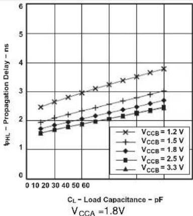
| C_L - Load Capacitance - pF | V_CC B = 1.2 V | V_CC B = 1.5 V | V_CC B = 1.8 V | V_CC B = 2.5 V | V_CC B = 3.3 V | | ---------------------------- | -------------- | -------------- | -------------- | -------------- | -------------- | | 10 | 2.7 | 2.3 | 2.0 | 1.9 | 1.8 | | 20 | 2.9 | 2.5 | 2.1 | 2.0 | 1.9 | | 30 | 3.1 | 2.7 | 2.2 | 2.1 | 2.0 | | 40 | 3.3 | 2.9 | 2.3 | 2.2 | 2.1 | | 50 | 3.5 | 3.1 | 2.4 | 2.3 | 2.2 | | 60 | 3.7 | 3.3 | 2.5 | 2.4 | 2.3 | | >60 | 4.0 | 3.5 | 2.6 | 2.5 | 2.4 |Figure4.TypicalPropagationDelay PHL (AtoB)vsLoad Capacitance

line
| C_L - Load Capacitance - pF | t_pLH - Propagation Delay - ns (V_CC = 1.2 V) | t_pLH - Propagation Delay - ns (V_CC = 1.5 V) | t_pLH - Propagation Delay - ns (V_CC = 1.8 V) | t_pLH - Propagation Delay - ns (V_CC = 2.5 V) | t_pLH - Propagation Delay - ns (V_CC = 3.3 V) | | ---------------------------- | ----------------------------------------------- | ----------------------------------------------- | ----------------------------------------------- | ----------------------------------------------- | ----------------------------------------------- | | 0 | 4.2 | 3.2 | 2.7 | 2.4 | 2.3 | | 10 | 4.4 | 3.4 | 2.9 | 2.5 | 2.4 | | 20 | 4.6 | 3.6 | 3.1 | 2.6 | 2.5 | | 30 | 4.8 | 3.8 | 3.3 | 2.7 | 2.6 | | 40 | 5.0 | 4.0 | 3.5 | 2.8 | 2.7 | | 50 | 5.2 | 4.2 | 3.7 | 2.9 | 2.8 | | 60 | 5.4 | 4.4 | 3.9 | 3.0 | 2.9 | | 70 | 5.6 | 4.6 | 4.1 | 3.1 | 3.0 | | 80 | 5.8 | 4.8 | 4.3 | 3.2 | 3.1 | | 90 | 6.0 | 5.0 | 4.5 | 3.3 | 3.2 | | 100 | 6.2 | 5.2 | 4.7 | 3.4 | 3.3 | | 110 | 6.4 | 5.4 | 4.9 | 3.5 | 3.4 | | 120 | 6.6 | 5.6 | 5.1 | 3.6 | 3.5 | | 130 | 6.8 | 5.8 | 5.3 | 3.7 | 3.6 | | 140 | 7.0 | 6.0 | 5.5 | 3.8 | 3.7 | | 150 | 7.2 | 6.2 | 5.7 | 3.9 | 3.8 | | 160 | 7.4 | 6.4 | 5.9 | 4.0 | 3.9 | | 170 | 7.6 | 6.6 | 6.1 | 4.1 | 4.0 | | 180 | 7.8 | 6.8 | 6.3 | 4.2 | 4.1 | | 190 | 8.0 | 7.0 | 6.5 | 4.3 | 4.2 | | 200 | 8.2 | 7.2 | 6.7 | 4.4 | 4.3 | | 210 | 8.4 | 7.4 | 6.9 | 4.5 | 4.4 | | 220 | 8.6 | 7.6 | 7.1 | 4.6 | 4.5 | | 230 | 8.8 | 7.8 | 7.3 | 4.7 | 4.6 | | 240 | 9.0 | 8.0 | 7.5 | 4.8 | 4.7 | | 250 | 9.2 | 8.2 | 7.7 | 4.9 | 4.8 | | 260 | 9.4 | 8.4 | 7.9 | 5.0 | 4.9 | | 270 | 9.6 | 8.6 | 8.1 | 5.1 | 5.0 | | 280 | 9.8 | 8.8 | 8.3 | 5.2 | 5.1 | | 290 | 10.0 | 9.0 | 8.5 | 5.3 | 5.2 | | 300 | 10.2 | 9.2 | 8.7 | 5.4 | 5.3 | | 310 | 10.4 | 9.4 | 8.9 | 5.5 | 5.4 | | 320 | 10.6 | 9.6 | 9.1 | 5.6 | 5.5 | | 330 | 10.8 | 9.8 | 9.3 | 5.7 | 5.6 | | 340 | 11.0 | 10.0 | 9.5 | 5.8 | 5.7 | | 350 | 11.2 | 10.2 | 9.7 | 5.9 | 5.8 | | 360 | 11.4 | 10.4 | 9.9 | 6.0 | 5.9 | | 370 | 11.6 | 10.6 | 10.1 | - | - | | 380 | - | - | - | - | - | | 390 | - | - | - | - | - | | 400 | - | - | - | - | - | | Note: The data is already provided in the code and cannot be extracted from the provided image in the given code format as it is not possible in the original image format for any given value of C_L and load capacitance.Figure5.TypicalPropagationDelay Capacitance PLH (AtoB)vsLoad
line
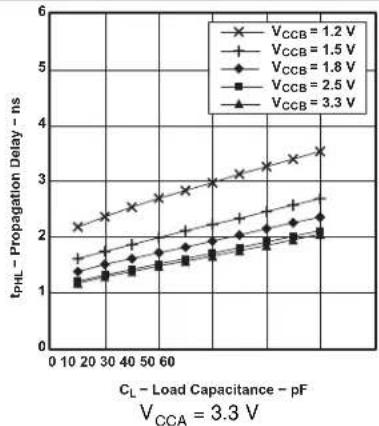
| CL - Load Capacitance - pF | tPHL - Propagation Delay - ns (VCCB = 1.2 V) | tPHL - Propagation Delay - ns (VCCB = 1.5 V) | tPHL - Propagation Delay - ns (VCCB = 1.8 V) | tPHL - Propagation Delay - ns (VCCB = 2.5 V) | tPHL - Propagation Delay - ns (VCCB = 3.3 V) | | --------------------------- | --------------------------------------------- | --------------------------------------------- | --------------------------------------------- | --------------------------------------------- | --------------------------------------------- | | 0 | 2.5 | 2.0 | 1.8 | 1.6 | 1.4 | | 20 | 2.7 | 2.2 | 2.0 | 1.8 | 1.6 | | 40 | 3.0 | 2.5 | 2.3 | 2.1 | 1.9 | | 60 | 3.3 | 2.8 | 2.6 | 2.4 | 2.2 | | 80 | 3.6 | 3.1 | 2.9 | 2.7 | 2.5 | | 100 | 3.9 | 3.4 | 3.2 | 3.0 | 2.8 | | 120 | 4.2 | 3.7 | 3.5 | 3.3 | 3.1 | | 140 | 4.5 | 4.0 | 3.8 | 3.6 | 3.4 | | 160 | 4.8 | 4.3 | 4.1 | 3.9 | 3.7 | | 180 | 5.1 | 4.6 | 4.4 | 4.2 | 4.0 | | 200 | 5.4 | 4.9 | 4.7 | 4.5 | 4.3 | | 220 | 5.7 | 5.2 | 5.0 | 4.8 | 4.6 | | 240 | 6.0 | 5.5 | 5.3 | 5.1 | 4.9 | | 260 | 6.3 | 5.8 | 5.6 | 5.4 | 5.2 | | 280 | 6.6 | 6.1 | 5.9 | 5.7 | 5.5 | | 300 | 6.9 | 6.4 | 6.2 | 6.0 | 5.8 | | 320 | 7.2 | 6.7 | 6.5 | 6.3 | 6.1 | | 340 | 7.5 | 7.0 | 6.8 | 6.6 | 6.4 | | 360 | 7.8 | 7.3 | 7.1 | 6.9 | 6.7 | | 380 | 8.1 | 7.6 | 7.4 | 7.2 | 7.0 | | 400 | 8.4 | 7.9 | 7.7 | 7.5 | 7.3 | | 420 | 8.7 | 8.2 | 8.0 | 7.8 | 7.6 | | 440 | 9.0 | 8.5 | 8.3 | 8.1 | 7.9 | | 460 | 9.3 | 8.8 | 8.6 | 8.4 | 8.2 | | 480 | 9.6 | 9.1 | 8.9 | 8.7 | 8.5 | | 500 | 9.9 | 9.4 | 9.2 | 9.0 | 8.8 | | 520 | 10.2 | 9.7 | 9.5 | 9.3 | 9.1 | | 540 | 10.5 | 10.0 | 9.8 | 9.6 | 9.4 | | 560 | 10.8 | 10.3 | 10.1 | 9.9 | 9.7 | | 580 | 11.1 | 10.6 | 10.4 | 10.2 | 10.0 | | 600 | 11.4 | 10.9 | 10.7 | 10.5 | 10.3 | | Note: The data is already in CSV format as it is provided in the code; the values are not explicitly provided in the code snippet from the original table above the code snippet array.Figure6.TypicalPropagationDelay Capacitance PHL (AtoB)vsLoad
Typical Characteristics (continued)
T_A=25^

Figure 7. Typical Propagation Delay t_PLH (A to B) vs Load Capacitance
line
| C_L - Load Capacitance - pF | t_PHL - Propagation Delay - ns (V_CC = 1.2 V) | t_PHL - Propagation Delay - ns (V_CC = 1.5 V) | t_PHL - Propagation Delay - ns (V_CC = 1.8 V) | t_PHL - Propagation Delay - ns (V_CC = 2.5 V) | t_PHL - Propagation Delay - ns (V_CC = 3.3 V) | | ---------------------------- | ----------------------------------------------- | ----------------------------------------------- | ----------------------------------------------- | ----------------------------------------------- | ----------------------------------------------- | | 0 | 2.4 | 1.9 | 1.6 | 1.4 | 1.2 | | 10 | 2.6 | 2.1 | 1.8 | 1.5 | 1.3 | | 20 | 2.8 | 2.3 | 2.0 | 1.7 | 1.4 | | 30 | 3.0 | 2.5 | 2.2 | 1.9 | 1.6 | | 40 | 3.2 | 2.7 | 2.4 | 2.1 | 1.8 | | 50 | 3.4 | 2.9 | 2.6 | 2.3 | 2.0 | | 60 | 3.6 | 3.1 | 2.8 | 2.5 | 2.2 | | >60 | ~3.8 | ~3.3 | ~3.0 | ~2.7 | ~2.4 |Figure 8. Typical Propagation Delay t_PHL (A to B) vs Load Capacitance

line
| C_I - Load Capacitance - pF | t_PLH - Propagation Delay - ns (V_CCB = 1.2 V) | t_PLH - Propagation Delay - ns (V_CCB = 1.5 V) | t_PLH - Propagation Delay - ns (V_CCB = 1.8 V) | t_PLH - Propagation Delay - ns (V_CCB = 2.5 V) | t_PLH - Propagation Delay - ns (V_CCB = 3.3 V) | | ---------------------------- | ----------------------------------------------- | ----------------------------------------------- | ----------------------------------------------- | ----------------------------------------------- | ----------------------------------------------- | | 0 | 3.8 | 2.6 | 2.1 | 1.7 | 1.4 | | 10 | 4.0 | 2.8 | 2.3 | 1.9 | 1.6 | | 20 | 4.2 | 3.0 | 2.5 | 2.1 | 1.8 | | 30 | 4.4 | 3.2 | 2.7 | 2.3 | 2.0 | | 40 | 4.6 | 3.4 | 2.9 | 2.5 | 2.2 | | 50 | 4.8 | 3.6 | 3.1 | 2.7 | 2.4 | | 60 | 5.0 | 3.8 | 3.3 | 2.9 | 2.6 | | 70 | 5.2 | 4.0 | 3.5 | 3.1 | 2.8 | | 80 | 5.4 | 4.2 | 3.7 | 3.3 | 3.0 | | 90 | 5.6 | 4.4 | 3.9 | 3.5 | 3.2 | | 100 | 5.8 | 4.6 | 4.1 | 3.7 | 3.4 | | 110 | 6.0 | 4.8 | 4.3 | 3.9 | 3.6 | | 120 | 6.2 | 5.0 | 4.5 | 4.1 | 3.8 | | 130 | 6.4 | 5.2 | 4.7 | 4.3 | 4.0 | | 140 | 6.6 | 5.4 | 4.9 | 4.5 | 4.2 | | 150 | 6.8 | 5.6 | 5.1 | 4.7 | 4.4 | | 160 | 7.0 | 5.8 | 5.3 | 4.9 | 4.6 | | 170 | 7.2 | 6.0 | 5.5 | 5.1 | 4.8 | | 180 | 7.4 | 6.2 | 5.7 | 5.3 | 5.0 | | 190 | 7.6 | 6.4 | 5.9 | 5.5 | 5.2 | | 200 | 7.8 | 6.6 | 6.1 | 5.7 | 5.4 | | 210 | 8.0 | 6.8 | 6.3 | 5.9 | 5.6 | | 220 | 8.2 | 7.0 | 6.5 | 6.1 | 5.8 | | 230 | 8.4 | 7.2 | 6.7 | 6.3 | 6.0 | | 240 | 8.6 | 7.4 | 6.9 | 6.5 | 6.2 | | 250 | 8.8 | 7.6 | 7.1 | 6.7 | 6.4 | | 260 | 9.0 | 7.8 | 7.3 | 6.9 | 6.6 | | 270 | 9.2 | 8.0 | 7.5 | 7.1 | 6.8 | | 280 | 9.4 | 8.2 | 7.7 | 7.3 | 7.0 | | 290 | 9.6 | 8.4 | 7.9 | 7.5 | 7.2 | | 300 | 9.8 | 8.6 | 8.1 | 7.7 | 7.4 | | 310 | 10.0 | 8.8 | 8.3 | 7.9 | 7.6 | | 320 | 10.2 | 9.0 | 8.5 | 8.1 | 7.8 | | 330 | 10.4 | 9.2 | 8.7 | 8.3 | 8.0 | | 340 | 10.6 | 9.4 | 8.9 | 8.5 | 8.2 | | 350 | 10.8 | 9.6 | 9.1 | 8.7 | 8.4 | | 360 | 11.0 | 9.8 | 9.3 | 8.9 | 8.6 | | 370 | 11.2 | 10.0 | 9.5 | 9.1 | 8.8 | | 380 | 11.4 | 10.2 | 9.7 | 9.3 | 9.0 | | 390 | 11.6 | 10.4 | 9.9 | 9.5 | 9.2 | | 400 | 11.8 | 10.6 | 10.1 | 9.7 | 9.4 | | Note: The data series are not explicitly provided in the code snippet, so I don't have a separate x-axis label for comparison purposes in the code format of the original y-axis variable (e.g., 'V_CCBA = .33 V'). The y-axis label is 'ns' and the x-axis label is 'Load Capacitance'. There is no label for the original y-axis variable in the code format as it is not explicitly labeled in the original y-axis variable.Figure 9. Typical Propagation Delay t_PLH (A to B) vs Load Capacitance
line
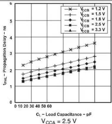
| C_L - Load Capacitance - pF | t_pHL - Propagation Delay - ns (V_CCB = 1.2 V) | t_pHL - Propagation Delay - ns (V_CCB = 1.5 V) | t_pHL - Propagation Delay - ns (V_CCB = 1.8 V) | t_pHL - Propagation Delay - ns (V_CCB = 2.5 V) | t_pHL - Propagation Delay - ns (V_CCB = 3.3 V) | | ---------------------------- | ----------------------------------------------- | ----------------------------------------------- | ----------------------------------------------- | ----------------------------------------------- | ----------------------------------------------- | | 0 | 2.2 | 1.7 | 1.4 | 1.2 | 1.0 | | 10 | 2.4 | 1.9 | 1.6 | 1.4 | 1.2 | | 20 | 2.6 | 2.1 | 1.8 | 1.6 | 1.4 | | 30 | 2.8 | 2.3 | 2.0 | 1.8 | 1.6 | | 40 | 3.0 | 2.5 | 2.2 | 2.0 | 1.8 | | 50 | 3.2 | 2.7 | 2.4 | 2.2 | 2.0 | | 60 | 3.4 | 2.9 | 2.6 | 2.4 | 2.2 | | >60 | ~3.6 | ~3.1 | ~2.8 | ~2.6 | ~2.4 |Figure 10. Typical Propagation Delay t_PHL (A to B) vs Load Capacitance
8 Parameter Measurement Information
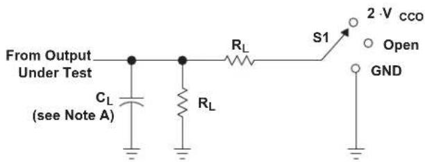
text_image
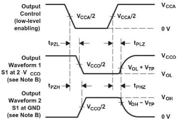
From Output Under Test CL (see Note A) RL RL S1 2·V cco Open GNDLOAD CIRCUIT
| V_CCO | C_L | R_L | V_TP |
| 1.2 V | 15 pF | 2 kΩ | 0.1 V |
| 1.5 V ±0.1 V | 15 pF | 2 kΩ | 0.1 V |
| 1.8 V ±0.15 V | 15 pF | 2 kΩ | 0.15 V |
| 2.5 V ±0.2 V | 15 pF | 2 kΩ | 0.15 V |
| 3.3 V ±0.3 V | 15 pF | 2 kΩ | 0.3 V |
| TEST S1 | |
| t_pd | Open |
| t_PLZ/t_PZL | 2·V cco |
| t_PHZ/t_PZH | GND |
text_image
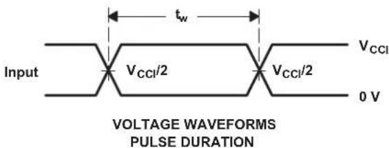
Input VCCl/2 tw VCCl/2 0 V VCCl VCCl VCCl VCCl VCCl VCCl VCCl VCCl VCCl VCCl VCCl VCCl VCCl VCCl VCCl VCCl VCCl VCCl VCCl VCCl VCCl VCCl VCCl VCCl VCCl VCCI VCCI VCCI VCCI VCCI VCCI VCCI VCCI VCCI VCCI VCCI VCCI VCCI VCCI VCCI VCCI VCCI VCCI VCCI VCCI VCCI VCCI VCCI VCCI VCCI VCCII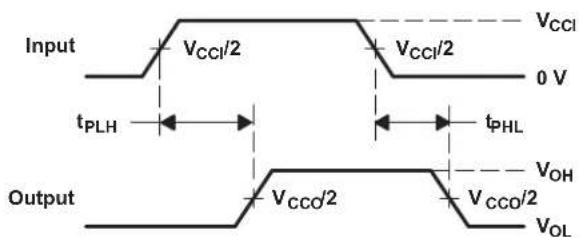
text_image
Input VCCI/2 VCCI/2 0 V tPLH tPHL Output VCCO/2 VOH VCCO/2 VOLVOLTAGE WAVEFORMS PROPAGATION DELAY TIMES
VOLTAGE WAVEFORMS
ENABLE AND DISABLE TIMES
NOTES: A. C L includes probe and jig capacitance.
B. Waveform 1 is for an output with internal conditions such that the output is low except when disabled by the output control. Waveform 2 is for an output with internal conditions such that the output is high, except when disabled by the output control.
C. All input pulses are supplied by generators having the following characteristics: PRR 10 MHz, ZO = 50 , dv/dt ≥ 1 V/ns.
D. The outputs are measured one at a time, with one transition per measurement.
E. t_PLH and t_PHL are the same as t_pd .
F. V_CCI is the V_CC associated with the input port.
G. V_CCO is the V_CC associated with the output port.
Figure 11. Load Circuit and Voltage Waveforms
9DetailedDescription
9.1 Overview
TheSN74AVC16T245isa16-bit,dual-supplynoninvertingbidirectionalvoltageleveltranslation.PinsAand controlpins(DIRandOE)aresupportedbyV CCA andpinsBaresupportedbyV CCB.TheAportcanacceptI/O voltagesrangingfrom1.2Vto3.6V,whiletheBportcanacceptI/Ovoltagesfrom1.2Vto3.6V.AhighonDIR allowsdatatransmissionfromAtoBandalowonDIRallowsdatatransmissionfromBtoAwhenOEissetto low.WhenOEissettohigh,bothAandBareinthehigh-impedancestate.
This device is fully specified for partial-power-down applications using off output current (I off).
TheV CC isolationfeatureensuresthatifeitherV CC inputisatGND,bothportsareputinahigh-impedancestate.
9.2 FunctionalBlockDiagram

flowchart
graph TD
    A["1DIR"] -->|1| B["AND Gate"]
    B --> C["48"]
    C --> D["1OE"]
    E["1A1"] -->|47| F["NOT Gate"]
    F --> G["2"]
    G --> H["1B1"]
    I["Ground"] --> J["Feedback Lines"]
    style A fill:#f9f,stroke:#333
    style B fill:#ccf,stroke:#333
    style C fill:#ccf,stroke:#333
    style D fill:#ccf,stroke:#333
    style E fill:#f9f,stroke:#333
    style F fill:#ccf,stroke:#333
    style G fill:#ccf,stroke:#333
    style H fill:#ccf,stroke:#333
    style I fill:#f9f,stroke:#333
To Seven Other Channels

text_image
2DIR 24 2OE 25 2A1 36 13 2B1To Seven Other Channels
9.3FeatureDescription
9.3.1 Fully Configurable Dual-Rail Design Allows Each Port to Operate Over the Full 1.2-V to 3.6-VPower-Supply Range
BothV CCA andV CCB can besupplied at any voltage from 1.2V to 3.6V making the devices suitable for translating between any of the low voltage nodes (1.2V, 1.8V, 2.5V, and 3.3V).
9.3.2 Partial-Power-DownModeOperation
This device is fully specified for partial-power-down applications using off output current (I off ). The I off circuitry will prevent backflow current by disabling / O output circuits when device is in partial power-down mode.
9.3.3V cc Isolation
TheV CC isolationfeatureensuresthatifeitherV CCA or V CCB areatGND,bothportswillbeinahigh-impedance state(I OZ shown in Electrical Characteristics). This prevents false logic levels from being presented to either bus.
9.4DeviceFunctionalModes
TheSN74AVC16T245isavoltageleveltranslatorthatcanoperatefrom1.2Vto3.6V(V CCA )and1.2Vto3.6V (V CCB ). Thesignaltranslationbetween1.2V and 3.6V requires direction control and output enableable control. When OE is low and DIR is high, data transmission is from A to B. When OE is low and DIR is low, data transmission is from B to A. When OE is high, both output port will be high-impedance.
Table1.FunctionsTable (1)
| CONTROLINPUTSOUTPUTCIRCUITS | OPERATION | |||
| ÕEDIRAPORTBPORT | ||||
| LLEnabledHi-Z | BdatatoAbus | |||
| L HHi-ZEnabled | AdatatoBbus | |||
| H XHi-Z | Hi-Z | Isolation | ||
(1) Inputcircuitsofthedatal/Os alwaysareactive.
10ApplicationandImplementation
NOTE
InformationinthefollowingapplicationssectionsisnotpartoftheTlcomponent specification,andTldoesnotwarrantitsaccuracyorcompleteness.TI'scustomersare responsiblefordeterminingsuitabilityofcomponentsfortheirpurposes.Customersshould validateandtesttheirdesignimplementationtoconfirmsystemfunctionality.
10.1 Application Information
TheSN74AVC16T245devicecanbeusedinlevel-shiftingapplicationsforinterfacingdevicesandaddressingmixedvoltageincompatibility.TheSN74AVC16T245deviceisidealfordatatransmissionwheredirectionisdifferentforeachchannel.
10.1.1 EnableTimes
Calculate the enable times for the SN74AVC16T45 using the following formulas:
| t_PZH (DIRtoA)=t | PLZ (DIRtoB)+t | PLH (BtoA)(1) |
| t_PZL (DIRtoA)=t | PHZ (DIRtoB)+t | PHL (BtoA)(2) |
| t_PZH (DIRtoB)=t | PLZ (DIRtoA)+t | PLH (AtoB)(3) |
| t_PZL (DIRtoB)=t | PHZ (DIRtoA)+t | PHL (AtoB)(4) |
Inabidirectional application, these enable times provide the maximum delay from the time the DIR bit switched until an output is expected. For example, if the SN74AVC16T245 initially is transmitting from A to B, then the DIR bit is switched; the B port of the device must be disabled before representing it with an input. After the B port has been disabled, an input signal applied to it appears on the corresponding A port after the specified propagation delay.
10.2 Typical Application
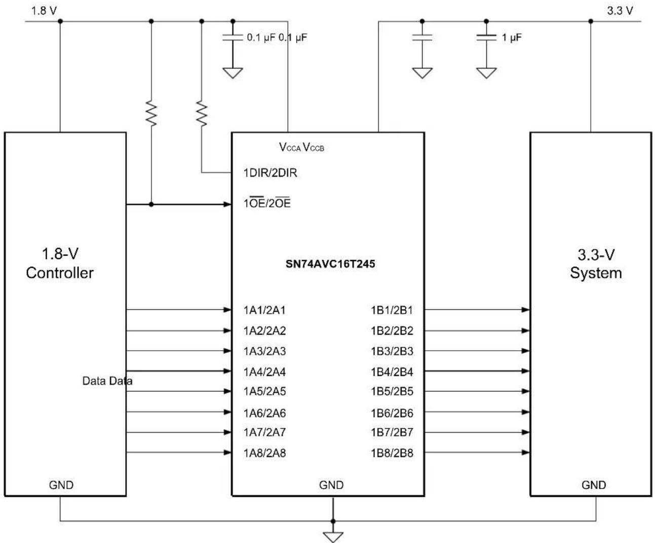
flowchart
graph TD
    A["1.8-V Controller"] -->|GND| B["SN74AVC16T245"]
    B -->|GND| C["3.3-V System"]
    D["Data Data"] -->|1A1/2A1| B
    D -->|1A2/2A2| B
    D -->|1A3/2A3| B
    D -->|1A4/2A4| B
    D -->|1A5/2A5| B
    D -->|1A6/2A6| B
    D -->|1A7/2A7| B
    D -->|1A8/2A8| B
    B -->|1B1/2B1| C
    B -->|1B2/2B2| C
    B -->|1B3/2B3| C
    B -->|1B4/2B4| C
    B -->|1B5/2B5| C
    B -->|1B6/2B6| C
    B -->|1B7/2B7| C
    B -->|1B8/2B8| C
    C -->|0.1 μF 0.1 μF| D
    D -->|0.1 μF 0.1 μF| E["Ground"]
    F["3.3 V"] --> G["Output"]
    H["1.8 V"] --> I["Ground"]
    J["0.1 μF 0.1 μF"] --> K["Ground"]
Figure12.TypicalApplicationSchematic
10.2.1 Design Requirements
This device uses drivers which are enabled depending on the state of the DIRpin. The designer must know the intended flow of data and take care not to violate any of the high or low logic levels. Unused data inputs must not be floating, asthiscan cause excessive internal leakage on the input CMOS structure. Tie any unused input and output ports directly to ground.
Forthisdesignexample, usetheparameterslisted in Table2.
Table2.DesignParameters
| DESIGNPARAMETEREXAMPLEVALUE |
| Inputvoltagerange1.2Vto3.6V |
| Outputvoltagerange1.2Vto3.6V |
10.2.2 Detailed Design Procedure
Tobeginthedesignprocess,determinethefollowing:
10.2.2.1 Input Voltage Ranges
Use the supply voltage of the device that is driving the SN74AVC16T245 device to determine the input voltage range. For a valid logic high the value must exceed the V in the input port. For a valid logic low the value must be less than the V in the input port.
10.2.2.2 Output Voltage Range
Use the supply voltage of the device that the SN74AVC16T245 device is driving to determine the output voltage range.
10.2.3ApplicationCurve

line
| Time (ns) | Input (1.2 V) (V) | Output (3.3 V) (V) | | --------- | ----------------- | ------------------ | | 0 | ~0.5 | ~0.5 | | 200 | ~0.5 | ~0.5 | | 2.50 | ~0.5 | ~0.5 | | 1.20 | ~0.5 | ~0.5 |Figure13. TranslationUp(1.2Vto3.3V)at2.5MHz
11 PowerSupplyRecommendations
TheSN74AVC16T245deviceusestwoseparateconfigurablepower-supplyrails, V CCA and V CCB .VCCAaccepts anysupplyvoltagefrom1.2Vto3.6VandV CCB acceptsanysupplyvoltagefrom1.2Vto3.6V.TheAportand BportaredesignedtotrackV CCA and V _CCB ,respectively,allowingforlow-voltagebidirectionaltranslation betweenanyofthe1.2-V,1.5-V,1.8-V,2.5-Vand3.3-Vvoltagenodes.
The output-enableOEinput circuit is designed so that it is supplied by V CCA and when the OE input is high, all outputs are placed in the high impedance state. To ensure the high impedance state of the output during power up or power down, the OE input must be tied to V CCA through a pullup resistor and must not be enabled until V CCA and V CCB are fully ramped and stable. The minimum value of the pullup resistor to V _CCA is determined by the current-sinking capability of the driver.
12Layout
12.1 LayoutGuidelines
Toensurereliabilityofthedevice,followingcommonprinted-circuit-boardlayoutguidelinesisrecommended.
- Bypasscapacitorsshouldbeusedonpowersupplies.
- Shorttracelengthsshouldbeusedtoavoidexcessiveloading.
- Placingpadsonthesignalpathsforloadingcapacitorsorpullupresistorstohelpadjustriseandfalltimesofsignalsdependingonthesystemrequirements.
12.2LayoutExample
text_image
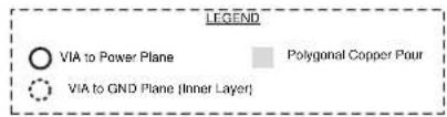
LEGEND VIA to Power Plane Polygonal Copper Pour VIA to GND Plane (Inner Layer)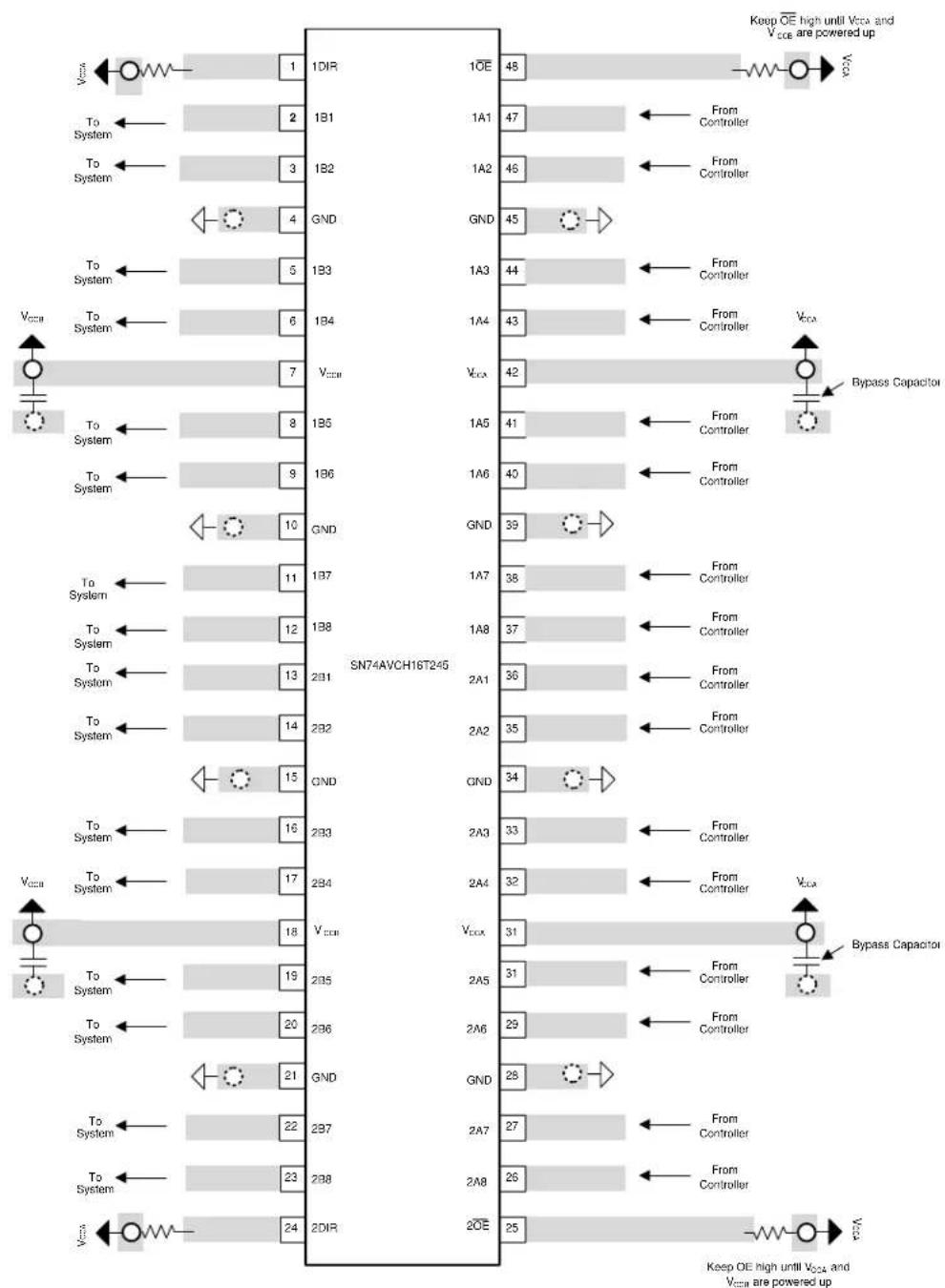
other
| Channel | Pin Number | Signal | Power Up (Vcc) | Power Down (VccB) | |---------|------------|--------|----------------|-------------------| | Left | 1 | VccA | - | - | | Left | 2 | To System | - | - | | Left | 3 | To System | - | - | | Left | 4 | GND | - | - | | Left | 5 | To System | - | - | | Left | 6 | To System | - | - | | Left | 7 | VccA | - | - | | Left | 8 | To System | - | - | | Left | 9 | To System | - | - | | Left | 10 | GND | - | - | | Left | 11 | To System | - | - | | Left | 12 | To System | - | - | | Left | 13 | To System | - | - | | Left | 14 | To System | - | - | | Left | 15 | GND | - | - | | Left | 16 | To System | - | - | | Left | 17 | To System | - | - | | Left | 18 | VccA | - | - | | Left | 19 | To System | - | - | | Left | 20 | To System | - | - | | Left | 21 | GND | - | - | | Left | 22 | To System | - | - | | Left | 23 | To System | - | - | | Left | 24 | VccA | - | - | | Right | 1 | VccA | 48 | - | | Right | 2 | To System | 47 | From Controller | | Right | 3 | To System | 46 | From Controller | | Right | 4 | GND | 45 | From Controller | | Right | 5 | To System | 44 | From Controller | | Right | 6 | To System | 43 | From Controller | | Right | 7 | VccA | 42 | From Controller | | Right | 8 | To System | 41 | From Controller | | Right | 9 | To System | 40 | From Controller | | Right | 10 | GND | 39 | From Controller | | Right | 11 | To System | 38 | From Controller | | Right | 12 | To System | 37 | From Controller | | Right | 13 | To System | 36 | From Controller | | Right | 14 | To System | 35 | From Controller | | Right | 15 | GND | 34 | From Controller | | Right | 16 | To System | 33 | From Controller | | Right | 17 | To System | 32 | From Controller | | Right | 18 | VccA | 31 | From Controller | | Right | 19 | To System | 31 | From Controller | | Right | 20 | To System | 29 | From Controller | | Right | 21 | GND | 28 | From Controller | | Right | 22 | To System | 27 | From Controller | | Right | 23 | To System | 26 | From Controller | | Right | 24 | VccA | 25 | From Controller | The chart includes labels for 'SN74AVCH16T245' and 'Keep OE high until VccA and VccB are powered up'.Figure14.RecommendedLayoutExample
13DeviceandDocumentationSupport
13.1 DocumentationSupport
13.1.1 Related Documentation
Forrelateddocumentationseethefollowing:
• CMOSPowerConsumptionandCpdCalculation,SCAA035
- Implications of Slowor Floating CMOS Inputs, SCBA004
13.2 Community Resources
The following links connect to TI community resources. Linked contents are provided "ASIS" by the respective contributors. They do not constitute TI specifications and do not necessarily reflect TI's views; see TI's Terms of Use.
TI E2E™ Online Community TI's Engineer-to-Engineer (E2E) Community. Created to foster collaboration amongengineers.Ate2e.ti.com,youcanaskquestions,shareknowledge,exploreideasandhelp solveproblemswithfellowengineers.
Design Support TI's Design Support Quickly find helpful E2E forums along with design support tools and contactinformationfortechnicalsupport.
13.3 Trademarks
E2EisatrademarkofTexasInstruments.
Allothertrademarksarethepropertyoftheirrespectiveowners.
13.4ElectrostaticDischargeCaution

These devices have limited built-in ESD protection. The leads should be shorted together or the device placed in conductive foam duringstorageorhandlingtopreventelectrostaticdamagetotheMOSgates.
13.5Glossary
SLYZ022—TIGlossary.
This glossarylistsandexplainsterms,acronyms,anddefinitions.
14Mechanical, Packaging, and Orderable Information
The following pages include mechanical, packaging, and orderable information. This information is the most current data available for the designated devices. This data is subject to changewithout notice and revision of this document. For browser-based versions of this datasheet, referto the left-hand navigation.
PACKAGING INFORMATION
| Orderable Device Status(1) | Package Type | Package Drawing | Pins | Package Qty | Eco Plan(2) | Lead finish/ Ball material(6) | MSL Peak Temp(3) | Op Temp (°C) | Device Marking(4-5) | Samples | |
| 74AVC16T245DGGRE4 ACTIVE TSSOP DGG 48 2000 RoHS & Green NIPDAU Level-1-260C-UNLIM -40 to 85 AVC16T245 | Samples | ||||||||||
| 74AVC16T245DGVRE4 ACTIVE TVSOP DGV 48 2000 RoHS & Green NIPDAU Level-1-260C-UNLIM -40 to 85 WF245 | Samples | ||||||||||
| AVC16T245DGGR-D | ACTIVE | TSSOP | DGG | 48 | 2000 | RoHS & Green | NIPDAU | Level-1-260C-UNLIM | -40 to 85 | AVC16T245 | Samples |
| SN74AVC16T245DGG | ACTIVE | TSSOP | DGG | 48 | 40 | RoHS & Green | NIPDAU | Level-1-260C-UNLIM | -40 to 85 | AVC16T245 | Samples |
| SN74AVC16T245DGGR | ACTIVE | TSSOP | DGG | 48 | 2000 | RoHS & Green | NIPDAU | Level-1-260C-UNLIM | -40 to 85 | AVC16T245 | Samples |
| SN74AVC16T245DGVR | ACTIVE | TVSOP | DGV | 48 | 2000 | RoHS & Green | NIPDAU | Level-1-260C-UNLIM | -40 to 85 | WF245 | Samples |
(1) The marketing status values are defined as follows:
ACTIVE: Product device recommended for new designs.
LIFEBUY: TI has announced that the device will be discontinued, and a lifetime-buy period is in effect.
NRND: Not recommended for new designs. Device is in production to support existing customers, but TI does not recommend using this part in a new design.
PREVIEW: Device has been announced but is not in production. Samples may or may not be available.
OBSOLETE: TI has discontinued the production of the device.
(2) RoHS: TI defines "RoHS" to mean semiconductor products that are compliant with the current EU RoHS requirements for all 10 RoHS substances, including the requirement that RoHS substance do not exceed 0.1% by weight in homogeneous materials. Where designed to be soldered at high temperatures, "RoHS" products are suitable for use in specified lead-free processes. TI may reference these types of products as "Pb-Free".
RoHS Exempt: TI defines "RoHS Exempt" to mean products that contain lead but are compliant with EU RoHS pursuant to a specific EU RoHS exemption.
Green: TI defines "Green" to mean the content of Chlorine (Cl) and Bromine (Br) based flame retardants meet JS709B low halogen requirements of <=1000ppm threshold. Antimony trioxide based flame retardants must also meet the <=1000ppm threshold requirement.
(3) MSL, Peak Temp. - The Moisture Sensitivity Level rating according to the JEDEC industry standard classifications, and peak solder temperature.
(4) There may be additional marking, which relates to the logo, the lot trace code information, or the environmental category on the device.
(5) Multiple Device Markings will be inside parentheses. Only one Device Marking contained in parentheses and separated by a "\~" will appear on a device. If a line is indented then it is a continuation of the previous line and the two combined represent the entire Device Marking for that device.
(6) Lead finish/Ball material - Orderable Devices may have multiple material finish options. Finish options are separated by a vertical ruled line. Lead finish/Ball material values may wrap to two lines if the finish value exceeds the maximum column width.

TEXAS INSTRUMENTS
www.ti.com
PACKAGE OPTION ADDENDUM
20-Jan-2021
Important Information and Disclaimer: The information provided on this page represents TI's knowledge and belief as of the date that it is provided. TI bases its knowledge and belief on information provided by third parties, and makes no representation or warranty as to the accuracy of such information. Efforts are underway to better integrate information from third parties. TI has taken and continues to take reasonable steps to provide representative and accurate information but may not have conducted destructive testing or chemical analysis on incoming materials and chemicals. TI and TI suppliers consider certain information to be proprietary, and thus CAS numbers and other limited information may not be available for release.
In no event shall TI's liability arising out of such information exceed the total purchase price of the TI part(s) at issue in this document sold by TI to Customer on an annual basis.
OTHER QUALIFIED VERSIONS OF SN74AVC16T245 :
• Automotive: SN74AVC16T245-Q1
NOTE: Qualified Version Definitions:
• Automotive - Q100 devices qualified for high-reliability automotive applications targeting zero defects
TAPE AND REEL INFORMATION

*All dimensions are nominal
| Device Package | Type | Package Drawing | Pins | SPQ Reel | Diameter (mm) | Reel Width W1 (mm) | A0 (mm) | B0 (mm) | K0 (mm) | P1 (mm) | W (mm) | Pin1 Quadrant |
| SN74AVC16T245DGGR | TSSOP DG | GG 48 2000 | 330.0 | 24.4 8.6 | 13.0 1.8 12.0 | 24.0 Q1 | ||||||
| SN74AVC16T245DGVR | TVSOP DG | V 48 2000 | 330.0 | 16.4 7.1 | 10.2 1.6 12.0 | 16.0 Q1 |

text_image
TAPE AND REEL BOX DIMENSIONS W L*All dimensions are nominal
| Device | Package Type | Package Drawing | Pins | SPQ | Length (mm) | Width (mm) | Height (mm) |
| SN74AVC16T245DGGR T | SSOP DGG 48 2000 | 367.0 367.0 45.0 | |||||
| SN74AVC16T245DGVR T | VSOP DGV 48 2000 | 853.0 449.0 35.0 |
TUBE
text_image
T - Tube height L - Tube length W - Tube width B - Alignment groove width*All dimensions are nominal
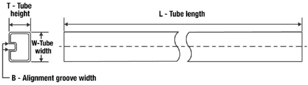
| Device | Package Name | Package Type | Pins | SPQ | L (mm) | W (mm) | T (μm) | B (mm) |
| SN74AVC16T245DGG D | GG TSSOP 48 40 5 | 30 11.89 3600 4 | .9 |
SMALL OUTLINE PACKAGE
text_image
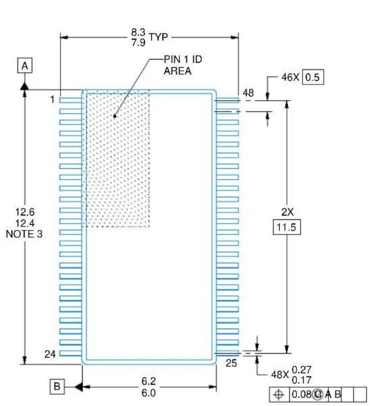
8.3 TYP 7.9 PIN 1 ID AREA 46X 0.5 1 48 2X 11.5 12.6 12.4 NOTE 3 24 25 48X 0.27 0.17 B 6.2 6.0 ⊕ 0.08@ A B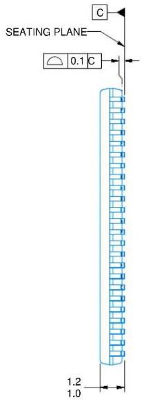
text_image
SEATING PLANE 0.1 C C 1.2 1.0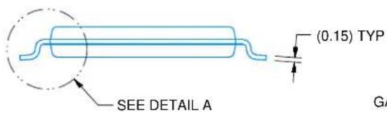
text_image
SEE DETAIL A (0.15) TYP GA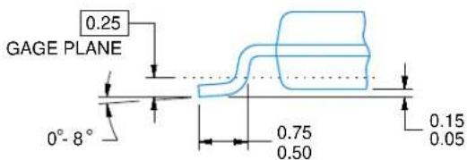
text_image
GAGE PLANE 0° - 8° 0.25 0.75 0.50 0.15 0.05DETAIL A TYPICAL
4214859/B 11/2020
NOTES:
- All linear dimensions are in millimeters. Any dimensions in parenthesis are for reference only. Dimensioning and tolerancing per ASME Y14.5M.
- This drawing is subject to change without notice.
- This dimension does not include mold flash, protrusions, or gate burrs. Mold flash, protrusions, or gate burrs shall not exceed 0.15 mm per side.
- Reference JEDEC registration MO-153.
SMALL OUTLINE PACKAGE

text_image
48X (1.5) 1 48X (0.3) 46X (0.5) (R0.05) TYP 24 SYMM 48 SYMM 25 (7.5)LAND PATTERN EXAMPLE SCALE:6X
text_image
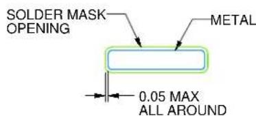
SOLDER MASK OPENING METAL 0.05 MAX ALL AROUNDNON SOLDER MASK DEFINED

text_image
METAL UNDER SOLDER MASK SOLDER MASK OPENING 0.05 MIN ALL AROUNDSOLDER MASK
DEFINED
SOLDER MASK DETAILS
4214859/B 11/2020
NOTES: (continued)
- Publication IPC-7351 may have alternate designs.
- Solder mask tolerances between and around signal pads can vary based on board fabrication site.
SMALL OUTLINE PACKAGE

text_image
48X (1.5) 1 48X (0.3) 46X (0.5) (R0.05) TYP 24 SYMM 48 SYMM 25 (7.5)SOLDER PASTE EXAMPLE BASED ON 0.125 mm THICK STENCIL SCALE:6X
4214859/B 11/2020
NOTES: (continued)
- Laser cutting apertures with trapezoidal walls and rounded corners may offer better paste release. IPC-7525 may have alternate design recommendations.
- Board assembly site may have different recommendations for stencil design.
DGG (R-PDSO-G\*\*) PLASTIC SMALL-OUTLINE PACKAGE
48 PINS SHOWN

text_image
0,50 48 0,27 0,17 ⊕ 0,08 Ⓜ 25 6,20 6,00 8,30 7,90 1 24 A 0,15 NOM Gage Plane 0,25 0°-8° 0,75 0,50 1,20 MAX Seating Plane 0,10 PINS ** DIM 48 56 64 A MAX 12,60 14,10 17,10 A MIN 12,40 13,90 16,90 4040078/F 12/97NOTES: A. All linear dimensions are in millimeters.
B. This drawing is subject to change without notice.
C. Body dimensions do not include mold protrusion not to exceed 0,15.
D. Falls within JEDEC MO-153
IMPORTANT NOTICE AND DISCLAIMER
TI PROVIDES TECHNICAL AND RELIABILITY DATA (INCLUDING DATA SHEETS), DESIGN RESOURCES (INCLUDING REFERENCE DESIGNS), APPLICATION OR OTHER DESIGN ADVICE, WEB TOOLS, SAFETY INFORMATION, AND OTHER RESOURCES "AS IS" AND WITH ALL FAULTS, AND DISCLAIMS ALL WARRANTIES, EXPRESS AND IMPLIED, INCLUDING WITHOUT LIMITATION ANY IMPLIED WARRANTIES OF MERCHANTABILITY, FITNESS FOR A PARTICULAR PURPOSE OR NON-INFRINGEMENT OF THIRD PARTY INTELLECTUAL PROPERTY RIGHTS.
These resources are intended for skilled developers designing with TI products. You are solely responsible for (1) selecting the appropriate TI products for your application, (2) designing, validating and testing your application, and (3) ensuring your application meets applicable standards, and any other safety, security, regulatory or other requirements.
These resources are subject to change without notice. TI grants you permission to use these resources only for development of an application that uses the TI products described in the resource. Other reproduction and display of these resources is prohibited. No license is granted to any other TI intellectual property right or to any third party intellectual property right. TI disclaims responsibility for, and you will fully indemnify TI and its representatives against, any claims, damages, costs, losses, and liabilities arising out of your use of these resources.
TI's products are provided subject to TI's Terms of Sale or other applicable terms available either on ti.com or provided in conjunction with such TI products. TI's provision of these resources does not expand or otherwise alter TI's applicable warranties or warranty disclaimers for TI products.
TI objects to and rejects any additional or different terms you may have proposed.
Mailing Address: Texas Instruments, Post Office Box 655303, Dallas, Texas 75265
Copyright © 2022, Texas Instruments Incorporated