SN74CB3Q3257PWR - Electronic component TEXAS INSTRUMENTS - Free user manual and instructions
Find the device manual for free SN74CB3Q3257PWR TEXAS INSTRUMENTS in PDF.

User questions about SN74CB3Q3257PWR TEXAS INSTRUMENTS
0 question about this device. Answer the ones you know or ask your own.
Ask a new question about this device
Download the instructions for your Electronic component in PDF format for free! Find your manual SN74CB3Q3257PWR - TEXAS INSTRUMENTS and take your electronic device back in hand. On this page are published all the documents necessary for the use of your device. SN74CB3Q3257PWR by TEXAS INSTRUMENTS.
USER MANUAL SN74CB3Q3257PWR TEXAS INSTRUMENTS
SN74CB3Q32574-Bit1-of-2FETMultiplexer/Demultiplexer
2.5-V/3.3-VLow-VoltageHigh-BandwidthBusSwitch
1Features
•High-BandwidthDataPath (upto500MHz)
- 5-VTolerantI/OsWithDevicePoweredUpon PoweredDown
- LowandFlatON-StateResistance(r on) CharacteristicsOverOperatingRange (r on=4Ω Typical)
- Rail-to-RailSwitchingonDatal/OPorts -0-to5-VSwitchingWith3.3-VV CC -0-to3.3-VSwitchingWith2.5-VV CC
- BidirectionalDataFlowWithNear-Zero PropagationDelay
- LowInputandOutputCapacitanceMinimizes LoadingandSignalDistortion ( C_io(OFF) = 3.5pFTypical )
- FastSwitchingFrequency(f Maximum) = 20MHz
- DataandControlInputsProvideUndershoot ClampDiodes
- LowPowerConsumption (Icc=0.7mATypical)
• V_cc OperatingRangeFrom2.3Vto3.6V
- DataI/OsSupport0-to5-VSignalingLevels (0.8V, 1.2V, 1.5V, 1.8V, 2.5V, 3.3V, 5V)
•ControlInputsCanBeDrivenbyTTLor 5-V/3.3-VCMOSOutputs
- I_off SupportsPartial-Power-DownModeOperation
- Latch-UpPerformanceExceeds100mAPer JESD78,ClassII
•ESDPerformanceTestedPerJESD22
-2000-VHumanBodyModel (A114-B,ClassII)
-1000-VCharged-DeviceModel(C101)
•SupportsBothDigitalandAnalogApplications: USBInterface, DifferentialSignalInterface, BusIsolation, Low-DistortionSignalGating (1)
(1) For additional information regarding the performance characteristics of the CB3Q family, refer to the T1 application report, CBT-C, CB3T, and CB3Q Signal-Switch Families, SCDA008.
2Applications
•IPPhones:WiredandWireless
•OpticalModules
•OpticalNetworking:VideoOverFiberandEPON
•PrivateBranchExchange(PBX)
•WiMAXandWirelessInfrastructureEquipment
3Description
TheSN74CB3Q3257deviceisahigh-bandwidthFET busswitchutilizingachargepumptoelevatethegate voltageofthepasstransistor,providingalowandflat ON-stateresistance(r on).
DeviceInformation (1)
| PARTNUMBER | PACKAGE | BODYSIZE(NOM) |
| SN74CB3Q3257DGVT | VSOP(16) | 3.60mm×4.40mm |
| SN74CB3Q3257DBQS | SOP(16) | 4.90mm×3.90mm |
| SN74CB3Q3257PW | TSSOP(16) | 5.00mm×4.40mm |
| SN74CB3Q3257RGYV | QFN(16) | 4.00mm×3.50mm |
(1) For all available packages, see the orderable addendum at the endofthedatasheet.
LogicDiagram(PositiveLogic)

flowchart
graph TD
    A["4"] --> B["SW"]
    C["7"] --> D["SW"]
    E["9"] --> F["SW"]
    G["12"] --> H["SW"]
    I["S"] --> J["NOT"]
    K["DE"] --> L["NOT"]
    B --> M["SW"]
    D --> N["SW"]
    F --> O["SW"]
    H --> P["SW"]
    J --> Q["OR"]
    L --> R["OR"]
    M --> S["AND"]
    N --> T["AND"]
    O --> U["AND"]
    P --> V["AND"]
    Q --> W["AND"]
    R --> X["AND"]
    S --> Y["AND"]
    T --> Z["AND"]
    U --> AA["AND"]
    V --> AB["AND"]
    W --> AC["AND"]
    X --> AD["AND"]
    Y --> AE["AND"]
    Z --> AF["AND"]
TableofContents
1 Features.... 1
2 Applications 1
3 Description 1
4 Revision History...... 2
5PinConfigurationandFunctions....3
6 Specifications.... 4
6.1 AbsoluteMaximumRatings....4
6.2ESDRatings....4
6.3RecommendedOperatingConditions....4
6.4ThermalInformation....5
6.5 Electrical Characteristics....5
6.6SwitchingCharacteristics,V CC=2.5V....6
6.7SwitchingCharacteristics,V CC =3.3V....6
6.8TypicalCharacteristics....6
7ParameterMeasurementInformation....7
8DetailedDescription....8
8.1 Overview....8
8.2FunctionalBlockDiagram....9
8.3FeatureDescription....9
8.4DeviceFunctionalModes....9
9ApplicationandImplementation....10
9.1 Application Information....10
9.2 Typical Application....10
10PowerSupplyRecommendations....11
11 Layout.... 11
11.1 LayoutGuidelines....11
11.2LayoutExample....11
12DeviceandDocumentationSupport....12
12.1 DocumentationSupport....12
12.2ReceivingNotificationofDocumentationUpdates12
12.3CommunityResources....12
12.4Trademarks....12
12.5ElectrostaticDischargeCaution....12
12.6Glossary....12
13Mechanical, Packaging, and Orderable Information 12
4RevisionHistory
ChangesfromRevisionC(April2017)toRevisionD
Page
- Changed the pinout images appearance .... 3
- Added Thermal Information table values .... 5
ChangesfromRevisionB(June2015)toRevisionC
Page
- AddedMAXvaluesforT _A = -40^ to 105^ to the Electrical Characteristics table 5
- AddedMAXvaluesforT A = -40^105^, V CC = 2.5 V table. 6
- Addedseparate Switching Characteristics, V CC =3.3V for V CC =3.3V±0.3V. Added TYP values and MAX values for T _A = -40°C to 105°C .... 6
ChangesfromRevisionA(November2003)toRevisionB
Page
- Removed Ordering Information table. 1
- Added Device Information table, Pin Configuration and Functions section, ESD Ratings table, Feature Description section, Device Functional Modes, Application and Implementation section, Power Supply Recommendations section, Layout section, Device and Documentation Support section, and Mechanical, Packaging, and Orderable Information section .... 1
5PinConfigurationandFunctions
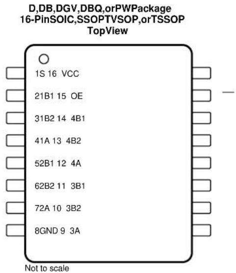
text_image
D,DB,DGV,DBQ,orPWPackage 16-PinSOIC,SSOPTVSOP,orTSSOP TopView 1S 16 VCC 21B1 15 OE 31B2 14 4B1 41A 13 4B2 52B1 12 4A 62B2 11 3B1 72A 10 3B2 8GND 9 3A Not to scale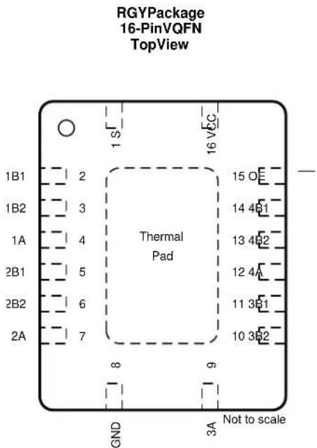
text_image
RGYPackage 16-PinVQFN TopView 1B1 2 1B2 3 1A 4 2B1 5 2B2 6 2A 7 1 S 16 VCC Thermal Pad 15 O 14 481 13 482 12 4A 11 381 10 382 8 9 GND 3A Not to scalePinFunctions
| PIN | I/O | DESCRIPTION | |
| NAME | NO. | ||
| S | 1 | I | SelectPin |
| 1B1 | 2 | I/O | Channel1I/O1 |
| 1B2 | 3 | I/O | Channel1I/O2 |
| 1A | 4 | I/O | Channel1common |
| 2B1 | 5 | I/O | Channel2I/O1 |
| 2B2 | 6 | I/O | Channel2I/O2 |
| 2A | 7 | I/O | Channel2common |
| GND | 8 | — | Ground |
| 3A | 9 | I/O | Channel3common |
| 3B2 | 10 | I/O | Channel3I/O2 |
| 3B1 | 11 | I/O | Channel3I/O1 |
| 4A | 12 | I/O | Channel4common |
| 4B2 | 13 | I/O | Channel4I/O2 |
| 4B1 | 14 | I/O | Channel4I/O1 |
| OE | 15 | I | OutputEnable(ActiveLow) |
| V_CC | 16 | — | Power |
6Specifications
6.1 AbsoluteMaximumRatings
overoperatingfree-airtemperaturerange(unlessotherwisenoted) (1)
| MINMAXUNIT | ||||||
| V_CC | Supplyvoltage-0.54.6V | |||||
| V_IN | Controlinputvoltage ^(2)(3) | -0.57 | V | |||
| V_I/O | SwitchI/Ovoltage ^(2)(3)(4) | -0.57 | V | |||
| I_IK | Controlinputclampcurrent | V | IN<0 | -50mA | ||
| I_I/OK | I/Oportclampcurrent | V | I/O<0 | -50mA | ||
| I_IO | ON-stateswitchcurrent | ±64mA | ||||
| ContinuouscurrentthroughV CC orGND | ±100 | mA | ||||
| T_stg | Storagetemperature | -65150 | °C | |||
(1) Stresses beyond those listed under Absolute Maximum Ratings may cause permanent damage to the device. These are stress ratings only, and functional operation of the device at these or any other conditions beyond those indicated under Recommended Operating Conditions is not implied. Exposure to absolute-maximum-rated conditions for extended periods may affect device reliability.
(2) Allvoltages are with respect to ground, unless otherwise specified.
(3) The input and output voltage ratings may be exceeded if the input and output clamp-current ratings are observed.
(4)V andV O areusedtodenotespecificconditionsforV I/O .
6.2ESDRatings
| VALUE | UNIT | ||
| V_(ESD) Electrostaticdischarge | Humanbodymodel(HBM),perANSI/ESDA/JEDECJS-001 (1) | ±2000 | V |
| Charged-devicemodel(CDM),perJEDECspecificationJESD22-C101(2) | ±1000 | ||
(1)JEDECdocumentJEP155statesthat500-VHBMallowssafemanufacturingwithastandardESDcontrolprocess.
(2)JEDECdocumentJEP157statesthat250-VCDMallowssafemanufacturingwithastandardESDcontrolprocess.
6.3 Recommended Operating Conditions
overoperatingfree-airtemperaturerange(unlessotherwisenoted) ^(1)
| MIN | MAX | UNIT | |||
| V_CC | Supplyvoltage | 2.3 | 3.6 | V | |
| V_IH | High-levelcontrolinputvoltage | V_CC=2.3Vto2.7V | 1.7 | 5.5 | V |
| V_CC=2.7Vto3.6V | 2 | 5.5 | |||
| V_IL | Low-levelcontrolinputvoltage | V_CC=2.3Vto2.7V | 0 | 0.7 | V |
| V_CC=2.7Vto3.6V | 0 | 0.8 | |||
| V_I/O | Datainput/outputvoltage | 0 | 5.5 | V | |
| T_A | Operating free-air temperature | -40 | 85 | °C | |
(1) AllunusedcontrolinputsofthedevicemustbeheldatV ImplicationsofSloworFloatingCMOSInputs, SCBA004. CC orGNDtoensureproperdeviceoperation. RefertotheTIapplicationreport,
6.4ThermalInformation
| THERMALMETRIC (1) | SN74CB3Q3257 | UNIT | ||||
| DBQ(SSOP) | DGV(TVSOP)PW(TSSOP)RGY(VQFN) | |||||
| 16PINS16PINS16PINS16PINS | ||||||
| R_ JA | Junction-to-ambientthermalresistance114.3126.01 | 12.749.1 | °C/W | |||
| R_ JC(top) | Junction-to-case (top) thermal resistance | 65.4 | 51.3 | 47.5 | 61.2 | |
| R_ JB | Junction-to-board thermal resistance | 56.8 | 57.8 | 57.8 | 25.9 | |
| _JT | Junction-to-top characterization parameter | 18.3 | 5.9 | 6.0 | 2.3 | |
| _JB | Junction-to-board characterization parameter | 56.4 | 57.3 | 57.3 | 26.0 | |
| R_ JC(bot) | Junction-to-case (bottom) thermal resistance | - | - | - | 11.4 | |
(1) For more information about traditional and new thermal metrics, see the Semiconductor and IC Package Thermal Metrics application report.
6.5 Electrical Characteristics
T_A = -40^ to 105^ . Typical values stated are over recommended operating free-air temperature range (unless otherwise noted) ^(1)
| PARAMETER | TESTCONDITIONS | MIN | TYP (2) | MAX | UNIT | ||
| V_IK | V_CC=3.6V,I_I=-18mA | -1.8 | V | ||||
| I_IN | Controlinputs | V_CC=3.6V,V_IN=0to5.5V | ±1 | μA | |||
| I_OZ^(3) | V_CC=3.6V,V_O=0to5.5V,V_I=0,SwitchOFFV_IN=V_CC orGND | ±1 | μA | ||||
| I_off | V_CC=0,V_O=0to5.5V,V_I=0 | 1 | μA | ||||
| I_CC | V_CC=3.6V,I_IO=0,SwitchONorOFF,V_IN=V_CC orGND | 0.7 | 1.5 | mA | |||
| I_CC^(4) | Controlinputs | V_CC=3.6V,Oneinputat3V,OtherinputsatV_CC orGND | 30 | μA | |||
| I_CCD^(5) | Percontrolinput | V_CC=3.6V,AandBportsopen,Controlinputswitchingat50%dutycycle | 0.3 | 0.35 | mA/MHz | ||
| C_in | Controlinputs | V_CC=3.3V,V_IN=5.5V,3.3V,or0 | 2.5 | 3.5 | pF | ||
| C_io(OFF) | Aport | V_CC=3.3V,SwitchOFF,V_IN=V_CC orGND,V_IO=5.5V,3.3V,or0 | 5.5 | 7 | pF | ||
| Bport | V_CC=3.3V,SwitchOFF,V_IN=V_CC orGND,V_IO=5.5V,3.3V,or0 | 3.5 | 5 | pF | |||
| C_io(ON) | Aport | V_CC=3.3V,SwitchON,V_IN=V_CC orGND,V_IO=5.5V,3.3V,or0 | 10.513 | pF | |||
| Bport | 10.513 | ||||||
| r_on^(6) | V_CC=2.3V,TYPatV_CC=2.5V | V_I=0,I_O=30mA | 4 | 8 | Ω | ||
| V_I=1.7V,I_O=-15mA | 4 | 9 | |||||
| V_CC=3V | V_I=0,I_O=30mA | 4 | 6 | ||||
| V_I=2.4V,I_O=-15mA | 4 | 8 | |||||
(1) V_IN and I_IN refertocontrolinputs. V_I, V_O, I, and I_O refertodataterminals.
(2) AlltypicalvaluesareatV =3.3V(unlessotherwisenoted),T =25°C.
(3)Forl/Oports, theparameterl _OZ includestheinputleakagecurrent.
(4) This is the increase in supply current for each input that is at the specified TTL voltage level, rather than V or GND.
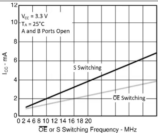
(5) This parameter specifies the dynamic power-supply current associated with the operating frequency of a single control input (see Figure2).
(6) Measured by the voltage drop between the A and B terminals at the indicated current through the switch. ON-state resistance is determined by the lower of the voltages of the two (AorB) terminals.
6.6SwitchingCharacteristics,V cc =2.5V
Typical values stated are over recommended operating free-air temperature range (unless otherwise noted) (see Figure 3)
| PARAMETER | FROM(INPUT) | TO(OUTPUT) | V_CC = 2.5V ± 0.2V | UNIT | ||
| MIN | MAX(85°C) | MAX(105°C) | ||||
| f_ or f_S^(1) | orSAorB10 | 10 MHz | ||||
| t_pd^(2) | A or B | B or A | 0.12 | 0.21 | ns | |
| t_pd(s) | S | A | 1.5 | 6.5 | 7.5 | ns |
| t_en | S | B | 1.5 | 6.5 | 7.5 | ns |
| A or B | 1.5 | 6.5 | 7.5 | |||
| t_dis | S | B | 1 | 6 | 7 | ns |
| A or B | 1 | 6 | 7 | |||
(1) Maximum switching frequency for control inputs (V O > VCC, V_I = 5V, R_L ≥ 1M, C_L = 0 ).
(2) The propagation delay is the calculated RC time constant of the typical on-state resistance of the switch and the specified load capacitance,whendrivenbyanidealvoltagesource(zerooutputimpedance).
6.7SwitchingCharacteristics,V cc =3.3V
Typicalvaluesstatedareoveroperatingfree-airtemperaturerange(unlessotherwisenoted)
| PARAMETER | FROM(INPUT) | TO(OUTPUT) | V_CC = 3.3V ± 0.3V | UNIT | |||
| MIN | TYP(1) | MAX(85°C) | MAX(105°C) | ||||
| f_ or f_S^(2) | or S | A or B | 20 | 20 | MHz | ||
| t_pd^(3) | A or B | B or A | 0.2 | 0.32 | ns | ||
| t_pd(s) | S | A | 1.5 | 4.1 | 5.5 | 6.5 | ns |
| t_en | S | B | 1.5 | 4.6 | 5.5 | 6.5 | ns |
| A or B | 1.5 | 4.7 | 5.5 | 6.5 | |||
| t_dis | S | B | 1 | 3.3 | 6 | 7 | ns |
| A or B | 1 | 3.1 | 6 | 7 | |||
(1) TYPtakenfromaveragein105°C
(2) Maximum switching frequency for control inputs (V O > VCC, V_I = 5V, R_L ≥ 1M, C_L = 0 ).
(3) The propagation delay is the calculated RC time constant of the typical on-state resistance of the switch and the specified load capacitance,whendrivenbyanidealvoltagesource(zerooutputimpedance).
6.8TypicalCharacteristics
line
| OE or S Switching Frequency - MHz | Icc - mA | | --------------------------------- | -------- | | 0 | 1.0 | | 6 | 1.5 | | 12 | 2.0 | | 18 | 2.5 | | 24 | 3.0 | | 30 | 3.5 | | 36 | 4.0 | | 42 | 4.5 | | 48 | 5.0 | | 54 | 5.5 | | 60 | 6.0 | | 66 | 6.5 | | 72 | 7.0 | | 78 | 7.5 | | 84 | 8.0 | | 90 | 8.5 | | 96 | 9.0 | | 102 | 9.5 | | 108 | 10.0 | | 114 | 10.5 | | 120 | 11.0 | | 126 | 11.5 | | 132 | 12.0 | | 138 | 12.5 | | 144 | 13.0 | | 150 | 13.5 | | 156 | 14.0 | | 162 | 14.5 | | 168 | 15.0 | | 174 | 15.5 | | 180 | 16.0 | | 186 | 16.5 | | 192 | 17.0 | | 198 | 17.5 | | 204 | 18.0 | | 210 | 18.5 | | 216 | 19.0 | | 222 | 19.5 | | 228 | 20.0 | | 234 | 20.5 | | 240 | 21.0 | | 246 | 21.5 | | 252 | 22.0 | | 258 | 22.5 | | 264 | 23.0 | | 270 | 23.5 | | 276 | 24.0 | | 282 | 24.5 | | 288 | 25.0 | | 294 | 25.5 | | 300 | 26.0 | | 306 | 26.5 | | 312 | 27.0 | | 318 | 27.5 | | 324 | 28.0 | | 330 | 28.5 | | 336 | 29.0 | | 342 | 29.5 | | 348 | 30.0 | | 354 | 30.5 | | 360 | 31.0 | | 366 | 31.5 | | 372 | 32.0 | | 378 | 32.5 | | 384 | 33.0 | | 390 | 33.5 | | 396 | 34.0 | | 402 | 34.5 | | 408 | 35.0 | | 414 | 35.5 | | 420 | 36.0 | | 426 | 36.5 | | 432 | 37.0 | | 438 | 37.5 | | 444 | 38.0 | | 450 | 38.5 | | 456 | 39.0 | | 462 | 39.5 | | 468 | 40.0 | | 474 | 40.5 | | 480 | 41.0 | | 486 | 41.5 | | 492 | 42.0 | | 498 | 42.5 | | 504 | 43.0 | | 510 | 43.5 | | 516 | 44.0 | | 522 | 44.5 | | 528 | 45.0 | | 534 | 45.5 | | 540 | 46.0 | | 546 | 46.5 | | 552 | 47.0 | | 558 | 47.5 | | 564 | 48.0 | | 570 | 48.5 | | 576 | 49.0 | | 582 | 49.5 | | 588 | 50.0 | | 594 | 50.5 | | 600 | 51.0 | | Note: The actual values may vary due to the current label 'E' or 'O' in the chart title, not explicitly provided in the code snippet.Figure1. Typicalr on vs V_I

line
| V_I - V | R_on - ON-State Resistance - Ω | | ------- | ------------------------------ | | 0.0 | 3.3 | | 0.5 | 3.4 | | 1.0 | 3.5 | | 1.5 | 3.6 | | 2.0 | 3.7 | | 2.5 | 3.8 | | 3.0 | 3.9 | | 3.5 | 4.0 | | 4.0 | 4.2 | | 4.5 | 4.8 | | 5.0 | 5.5 | | 5.5 | 6.5 | | 6.0 | 7.5 |Figure2. Typicall cc vsOEorSSwitchingFrequency
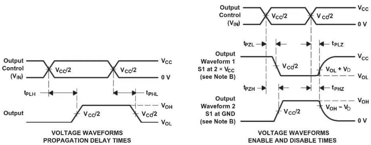
7 Parameter Measurement Information

text_image
Input Generator VG1 50 Ω V_IN 50 Ω DUT TEST CIRCUIT VCC V_G2 50 Ω V_I 50 Ω V_O R_L S1 CL (see Note A) 2 × V_CC Open GND| TEST | V_CC | S1 | R_L | V_I | C_L | V_ |
| t_pd(s) | 2.5 V ± 0.2 V3.3 V ± 0.3 V | OpenOpen | 500 Ω500 Ω | V_CC or GND V_CC or GND | 30 pF50 pF | |
| t_PLZ/t_PZL | 2.5 V ± 0.2 V3.3 V ± 0.3 V | 2 × V_CC 2 × V_CC | 500 Ω500 Ω | GNDGND | 30 pF50 pF | 0.15 V0.3 V |
| t_PHZ/t_PZH | 2.5 V ± 0.2 V3.3 V ± 0.3 V | GNDGND | 500 Ω500 Ω | V_CC V_CC | 30 pF50 pF | 0.15 V0.3 V |
text_image
Output Control (VIN) VCC/2 VCC/2 0 V tPLH tPHL Output VCC/2 VCC/2 VCL/2 VOL VCC/2 VCC/2 VCC Output Control (VIN) VCC/2 VCC/2 0 V tPZL tPLZ Output Waveform 1 S1 at 2 × VCC (see Note B) VCC/2 VCL/2 VOL + VD VOL tPZH tPHZ Output Waveform 2 S1 at GND (see Note B) VCC/2 VCC/2 VCL/2 VCL/2 VOL - VD VOH VOH VOL VCC/2 VCC/2 0 V VCC VCC VCL/2 VCC/2 0 VNOTES: A. C _L includes probe and jig capacitance.
B. Waveform 1 is for an output with internal conditions such that the output is low except when disabled by the output control.
Waveform 2 is for an output with internal conditions such that the output is high, except when disabled by the output control.
C. All input pulses are supplied by generators having the following characteristics: PRR≤10 MHz, Z_O=50 W, t≤2.5 ns, t≤2.5 ns.
D. The outputs are measured one at a time, with one transition per measurement.
E. t_PLZ and t_PHZ are the same as t_dis
F. t_PZL and t_PZH are the same as t_en
G. t_PLH and t_PHL are the same as t_pd(s) . The t_pd propagation delay is the calculated RC time constant of the typical ON-state resistant of the switch and the specified load capacitance, when driven by an ideal voltage source (zero output impedance).
H. All parameters and waveforms are not applicable to all devices.
Figure 3. Load Circuit and Voltage Waveforms
8DetailedDescription
8.1 Overview
TheSN74CB3Q3257deviceisahigh-bandwidthFETbusswitchusingachargepumptoelevatethegate voltageofthepasstransistor,providingalowandflatON-stateresistance(r on).ThelowandflatON-state resistanceallowsforminimalpropagationdelayandsupportsrail-to-railswitchingonthedatainput/output(I/O) ports. Thedevicealsofeatureslowdatal/Ocapacitancetominimizecapacitiveloadingandsignaldistortionon thedatabus. Specificallydesignedtosupporthigh-bandwidthapplications,theSN74CB3Q3257deviceprovides anoptimizedinterfacesolutionideallysuitedforbroadbandcommunications,networking,anddata-intensive computingsystems.
TheSN74CB3Q3257deviceisorganizedastwo1-of-4multiplexers/demultiplexerswithseparateoutput-enable(1OE,2OE)inputs. Theselect(S0,S1)inputscontrolledatapathofeachmultiplexer/demultiplexer.WhenOE islow,theassociatedmultiplexer/demultiplexerisenabled,andtheAportisconnectedtotheBport,allowing bidirectionaldataflowbetweenports.WhenOEishigh,theassociatedmultiplexer/demultiplexererisdisabled,and ahigh-impedancestateexistsbetweentheAandBports.
This device is fully specified for partial-power-down applications using l_off . The l_off circuitry prevents damaging current backflow through the device when it is powered down. The device has isolation during power off.
Toensure the high-impedance stated during power up or power down, OE should be tied to V _CC through a pull-up resistor; the minimum value of the resistor is determined by the current-sinking capability of the driver.

text_image
A VCC Charge Pump B EN(1)(1)ENistheinternalenablesignalappliedtotheswitch.
Figure4.SimplifiedSchematic,EachFETSwitch(SW)
8.2FunctionalBlockDiagram

flowchart
graph TD
    A["4"] --> B["SW"]
    C["7"] --> D["SW"]
    E["9"] --> F["SW"]
    G["12"] --> H["SW"]
    I["S"] --> J["NOT"]
    K["OE"] --> L["NOT"]
    B --> M["SW"]
    D --> N["SW"]
    F --> O["SW"]
    H --> P["SW"]
    J --> Q["NOT"]
    L --> R["NOT"]
    M --> S["AND"]
    N --> T["AND"]
    O --> U["AND"]
    P --> V["AND"]
    Q --> W["AND"]
    R --> X["AND"]
    S --> Y["OR"]
    T --> Z["OR"]
    U --> AA["OR"]
    V --> AB["OR"]
    W --> AC["OR"]
    X --> AD["OR"]
    Y --> AE["OR"]
    Z --> AF["OR"]
    AA --> AG["OR"]
    AB --> AH["OR"]
    AC --> AI["OR"]
    AD --> AJ["OR"]
    AE --> AK["OR"]
8.3FeatureDescription
TheSN74CB3Q3257devicehasahigh-bandwidthdatapath(upto500MHz)andhas5-Vtolerantl/Oswiththe devicepowereduporpowereddown.ItalsohaslowandflatON-stateresistance(r on)characteristicsover operatingrange(r on =4Ω Typical).
This device also has rail-to-rail switching on data/0 ports for 0 to 5 V switching with 3.3 V switching with 2.5 V as well as bidirectional data flow with near-zero propagation delay and low input capacitance that minimizes loading and signal distortion (C _io(OFF) = 3.5 pF Typical).
TheSN74CB3Q3257alsoprovidesafastswitchingfrequency(f =20MHzMax )withdataandcontrolinputs thatprovideundershootclampdiodesaswellaslowpowerconsumption(I _CC=0.6mATypical ).
TheV CC operatingrangeisfrom2.3Vto3.6Vandthedatal/Ossupport0-to5-Vsignallevelsof(0.8-V,1.2-V,1.5-V,1.8-V,2.5-V,3.3-V,5-V).
The control input scan bed driven by TTL or 5-V/3.3-VCMOS outputs as well as I Down Mode Operation. off Supports Partial-Power-
8.4DeviceFunctionalModes
Table1liststhefunctionalmodesoftheSN74CB3Q3257.
Table1.FunctionTable
| INPUTS | INPUT/OUTPUTA | FUNCTION | |
| OE | S | ||
| LL | B1 Aport=B1port | ||
| L | H | B2 | Aport=B2port |
| H | X | Z | Disconnect |
9ApplicationandImplementation
NOTE
InformationinthefollowingapplicationssectionsisnotpartoftheTlcomponent specification,andTldoesnotwarrantitsaccuracyorcompleteness.TI'scustomersare responsiblefordeterminingsuitabilityofcomponentsfortheirpurposes.Customersshould validateandtesttheirdesignimplementationtoconfirmsystemfunctionality.
9.1 Application Information
TheSN74CB3Q3257canbeusedtomultiplexanddemultiplexupto4channelssimultaneouslyina2:1 configuration. Theapplicationsownhereisa4-bitbusbeingmultiplexedbetweenwodevices.theOEandSpinsareusedtocontrolthechipfromthebuscontroller. Thisisaverygenericexample,andcouldapplytomany situations. Ifanapplicationrequireslessthan4bits,besuretotietheAsidetoeitherhighorlowonunused channels.
9.2 Typical Application
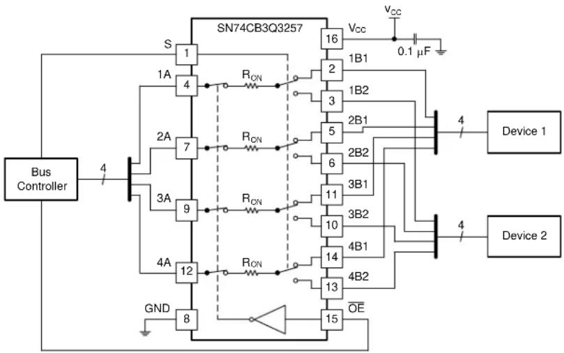
text_image
SN74CB3Q3257 Vcc 0.1 µF S 1 1A 4 RcN 2 1B1 2 1B2 3 2B1 5 2B2 6 3B1 7 RcN 9 RcN 11 3B2 10 4B1 14 4B2 13 OE 4 Device 1 4 Device 2 Bus Controller 4 GND 8Figure5.TypicalApplicationoftheSN74CB3Q3257
9.2.1 DesignRequirements
- RecommendedInputConditions:
-Forspecifiedhighandlowlevels,seeV IH andV IL inRecommendedOperatingConditions.
-Inputsandoutputsareovervoltagetolerantslowingthemtogoashighas4.6VatanyvalidV cc .
- RecommendedOutputConditions:
-Loadcurrentsshouldnotexceed±128mAperchannel.
- FrequencySelectionCriterion:
-Maximumfrequencytestedis500MHz.
-Addedtraceresistance/capacitancecanreducemaximumfrequencycapability;uselayoutpracticesas directedinLayout.
9.2.2 Detailed Design Procedure
The0.1-μFcapacitorshouldbeplaceascloseaspossibletothedevice.
TypicalApplication(continued)
9.2.3ApplicationCurve

line
| Time (ps) | VIN Voltage (V) | VOUT Voltage (V) | | --------- | --------------- | ---------------- | | 0 | 0 | 0 | | 100 | 0 | 0 | | 200 | 0 | 0 | | 300 | 0 | 0 | | 400 | 0 | 0 | | 500 | 0 | 0 | | 600 | 2.5 | 0 | | 700 | 2.5 | 2.5 | | 800 | 2.5 | 2.5 | | 900 | 2.5 | 2.5 | | 1000 | 2.5 | 2.5 |Figure6. PropagationDelay(t pd ) SimulationResultatV cc =2.5V.
10PowerSupplyRecommendations
ThepowersupplycanbeanyvoltagebetweentheminimumandmaximumsupplyvoltageratinglistedintheAbsoluteMaximumRatingstable.
EachV CC terminal should have good bypass capacitort to prevent power disturbance. For devices with a single supply, a0.1-μF bypass capacitor is recommended. If multiple pins are labeled V CC then a0.01-μFor 0.022-μF capacitor is recommended for each V CC because the V CC pins are tied together internally. For devices with dual-supply pins operating at different voltages, forexample V CC and V DD, a0.1-μF bypass capacitor is recommended for each supply pin. Toreject different frequencies of noise, use multiple bypass capacitors in parallel. Capacitors with values of 0.1 μF and 1 μF are commonly used in parallel. The bypass capacitor should be installed as close to the power terminal as possible for best results.
11Layout
11.1 LayoutGuidelines
Reflectionsandmatchingarecloselyrelatedtotheloopantennatheorybutaredifferentenoughtobediscussed separatelyfromthetheory.WhenaPCBtraceturnsacornerata90°angle,areflectioncanoccur.Areflection occursprimarilybecauseofthechangeofwidthofthetrace.Attheapexoftheturn,thetracedwidthincreasesto 1.414timesthewidth.Thisincreaseupsetsthetransmission-linecharacteristics,especiallythedistributed capacitance and self-inductance of the trace which results in the reflection. Not all PCB traces can be straight and therefore some traces must turn corners. Figure 7 shows progressively better techniques of rounding corners.Onlythelastexample(BEST)maintainsconstanttracewidthandminimizesreflections.
11.2LayoutExample

text_image
WORST 2W BETTER 1W min. W BESTFigure7.TraceExample
12DeviceandDocumentationSupport
12.1 DocumentationSupport
12.1.1 Related Documentation
Forrelateddocumentationseethefollowing:
- Implications of Slowor Floating CMOS Inputs, SCBA004
- SelectingtheRightTexasInstrumentsSignalSwitch,SZZA030
12.2ReceivingNotificationofDocumentationUpdates
Toreceivenotificationofdocumentationupdates,navigatetothedeviceproductfolderonti.com.Intheupper right corner, click on Alert me to register and receive a weekly digest of any product information that has changed.Forchangedetails,reviewtherevisionhistoryincludedinanyreviseddocument.
12.3 Community Resources
The following links connect to TI community resources. Linked contents are provided "ASIS" by the respective contributors. They do not constitute TI specifications and do not necessarily reflect TI's views; see TI's Terms of Use.
TI E2E™ Online Community TI's Engineer-to-Engineer (E2E) Community. Created to foster collaboration amongengineers.Ate2e.ti.com,youcanaskquestions,shareknowledge,exploreideasandhelp solveproblemswithfellowengineers.
Design Support TI's Design Support Quickly find helpful E2E forums along with design support tools and contactinformationfortechnicalsupport.
12.4Trademarks
E2EisatrademarkofTexasInstruments.
Allothertrademarksarethepropertyoftheirrespectiveowners.
12.5ElectrostaticDischargeCaution

These devices have limited built-in ESD protection. The leads should be shorted together or the device placed in conductive foam duringstorageorhandlingtopreventelectrostaticdamagetotheMOSgates.
12.6Glossary
SLYZ022—TIGlossary.
This glossarylistsandexplainsterms,acronyms,anddefinitions.
13Mechanical, Packaging, and Orderable Information
The following pages include mechanical, packaging, and orderable information. This information is the most current data available for the designated devices. This data subject to changewithout notice and revision of this document. For browser-based versions of this datasheet, referto the left-hand navigation.
PACKAGING INFORMATION
| Orderable Device Status(1) | Package Type | Package Drawing | Pins | Package Qty | Eco Plan(2) | Lead finish/ Ball material(6) | MSL Peak Temp(3) | Op Temp (°C) | Device Marking(4-5) | Samples | |
| 74CB3Q3257DBQRE4 ACTIVE SSOP DBQ 16 2500 RoHS & Green NIPDAU Level-2-260C-1 YEAR -40 to 85 BU257 | Samples | ||||||||||
| 74CB3Q3257RGYRG4 ACTIVE VQFN RGY 16 3000 RoHS & Green NIPDAU Level-2-260C-1 YEAR -40 to 85 BU257 | Samples | ||||||||||
| SN74CB3Q3257DBQR ACTIVE SSOP DBQ 16 2500 RoHS & Green NIPDAU Level-2-260C-1 YEAR -40 to 85 BU257 | Samples | ||||||||||
| SN74CB3Q3257DGVR | ACTIVE | TVSOP | DGV | 16 | 2000 | RoHS & Green | NIPDAU | Level-1-260C-UNLIM | -40 to 85 | BU257 | Samples |
| SN74CB3Q3257PW | ACTIVE | TSSOP | PW | 16 | 90 | RoHS & Green | NIPDAU | Level-1-260C-UNLIM | -40 to 85 | BU257 | Samples |
| SN74CB3Q3257PWE4 | ACTIVE | TSSOP | PW | 16 | 90 | RoHS & Green | NIPDAU | Level-1-260C-UNLIM | -40 to 85 | BU257 | Samples |
| SN74CB3Q3257PWG4 | ACTIVE | TSSOP | PW | 16 | 90 | RoHS & Green | NIPDAU | Level-1-260C-UNLIM | -40 to 85 | BU257 | Samples |
| SN74CB3Q3257PWR | ACTIVE | TSSOP | PW | 16 | 2000 | RoHS & Green | NIPDAU | SN | Level-1-260C-UNLIM | -40 to 85 | BU257 | Samples |
| SN74CB3Q3257PWRG4 | ACTIVE | TSSOP | PW | 16 | 2000 | RoHS & Green | NIPDAU | Level-1-260C-UNLIM | -40 to 85 | BU257 | Samples |
| SN74CB3Q3257RGYR | ACTIVE | VQFN | RGY | 16 | 3000 | RoHS & Green | NIPDAU | Level-2-260C-1 YEAR | -40 to 85 | BU257 | Samples |
(1) The marketing status values are defined as follows:
ACTIVE: Product device recommended for new designs.
LIFEBUY: TI has announced that the device will be discontinued, and a lifetime-buy period is in effect.
NRND: Not recommended for new designs. Device is in production to support existing customers, but TI does not recommend using this part in a new design.
PREVIEW: Device has been announced but is not in production. Samples may or may not be available.
OBSOLETE: TI has discontinued the production of the device.
(2) RoHS: TI defines "RoHS" to mean semiconductor products that are compliant with the current EU RoHS requirements for all 10 RoHS substances, including the requirement that RoHS substance do not exceed 0.1% by weight in homogeneous materials. Where designed to be soldered at high temperatures, "RoHS" products are suitable for use in specified lead-free processes. TI may reference these types of products as "Pb-Free".
RoHS Exempt: TI defines "RoHS Exempt" to mean products that contain lead but are compliant with EU RoHS pursuant to a specific EU RoHS exemption.
Green: TI defines "Green" to mean the content of Chlorine (Cl) and Bromine (Br) based flame retardants meet JS709B low halogen requirements of <=1000ppm threshold. Antimony trioxide based flame retardants must also meet the <=1000ppm threshold requirement.
(3) MSL, Peak Temp. - The Moisture Sensitivity Level rating according to the JEDEC industry standard classifications, and peak solder temperature.
(4) There may be additional marking, which relates to the logo, the lot trace code information, or the environmental category on the device.

TEXAS INSTRUMENTS
www.ti.com
PACKAGE OPTION ADDENDUM
10-Dec-2020
(5) Multiple Device Markings will be inside parentheses. Only one Device Marking contained in parentheses and separated by a “\~” will appear on a device. If a line is indented then it is a continuation of the previous line and the two combined represent the entire Device Marking for that device.
(6) Lead finish/Ball material - Orderable Devices may have multiple material finish options. Finish options are separated by a vertical ruled line. Lead finish/Ball material values may wrap to two lines if the finish value exceeds the maximum column width.
Important Information and Disclaimer: The information provided on this page represents TI's knowledge and belief as of the date that it is provided. TI bases its knowledge and belief on information provided by third parties, and makes no representation or warranty as to the accuracy of such information. Efforts are underway to better integrate information from third parties. TI has taken and continues to take reasonable steps to provide representative and accurate information but may not have conducted destructive testing or chemical analysis on incoming materials and chemicals. TI and TI suppliers consider certain information to be proprietary, and thus CAS numbers and other limited information may not be available for release.
In no event shall TI's liability arising out of such information exceed the total purchase price of the TI part(s) at issue in this document sold by TI to Customer on an annual basis.
TAPE AND REEL INFORMATION
*All dimensions are nominal
| Device Package | Type | Package Drawing | Pins | SPQ Reel | Diameter (mm) | Reel Width W1 (mm) | A0 (mm) | B0 (mm) | K0 (mm) | P1 (mm) | W (mm) | Pin1 Quadrant |
| SN74CB3Q3257DBQR S | SOP DBC | 16 2500 3 | 30.0 | 12.5 6.4 5.2 | 2.1 8.0 12.0 Q1 | |||||||
| SN74CB3Q3257DGVR T | VSOP DGV | 16 2000 | 330.0 | 12.4 6.8 4.0 | 1.6 8.0 12.0 Q1 | |||||||
| SN74CB3Q3257PWR T | SSOP PW | 16 2000 3 | 30.0 | 12.4 6.9 5.6 | 1.6 8.0 12.0 Q1 | |||||||
| SN74CB3Q3257PWR T | SSOP PW | 16 2000 3 | 30.0 | 12.4 6.9 5.6 | 1.6 8.0 12.0 Q1 | |||||||
| SN74CB8Q3257PWRG4 | TSSOP PW | 16 2000 | 33 | 30.0 12.4 6.9 | 5.6 1.6 | 8.0 12.0 Q1 | ||||||
| SN74CB3Q3257RGYR V | QFN RGY | 16 3000 | 33 | 30.0 12.4 3.8 | 4.3 1.5 8.0 | 12.0 Q1 |
text_image
TAPE AND REEL BOX DIMENSIONS W L*All dimensions are nominal
| Device | Package Type | Package Drawing | Pins | SPQ | Length (mm) | Width (mm) | Height (mm) |
| SN74CB3Q3257DBQR S | SOP DBQ 16 2500 | 340.5 338.1 20.6 | |||||
| SN74CB3Q3257DGVR T | VSOP DGV 16 2000 | 367.0 367.0 35.0 | |||||
| SN74CB3Q3257PWR TS | SOP PW 16 2000 | 364.0 364.0 27.0 | |||||
| SN74CB3Q3257PWR TS | SOP PW 16 2000 | 367.0 367.0 35.0 | |||||
| SN74CB3Q3257PWRG4 | TSSOP PW | 16 2000 36 | 7.0 367.0 35.0 | ||||
| SN74CB3Q3257RGYR V | QFN RGY 16 3000 | 367.0 367.0 35.0 |
TUBE

text_image
T - Tube height L - Tube length W-Tube width B - Alignment groove width*All dimensions are nominal
| Device | Package Name | Package Type | Pins | SPQ | L (mm) | W (mm) | T (μm) | B (mm) |
| SN74CB3Q3257PW PW | TSSOP 16 90 530 | 10.2 3600 3.5 | ||||||
| SN74CB3Q3257PWE4 PW | TSSOP 16 90 530 | 10.2 3600 3.5 | ||||||
| SN74CB3Q3257PWG4 PW | TSSOP 16 90 530 | 10.2 3600 3.5 |
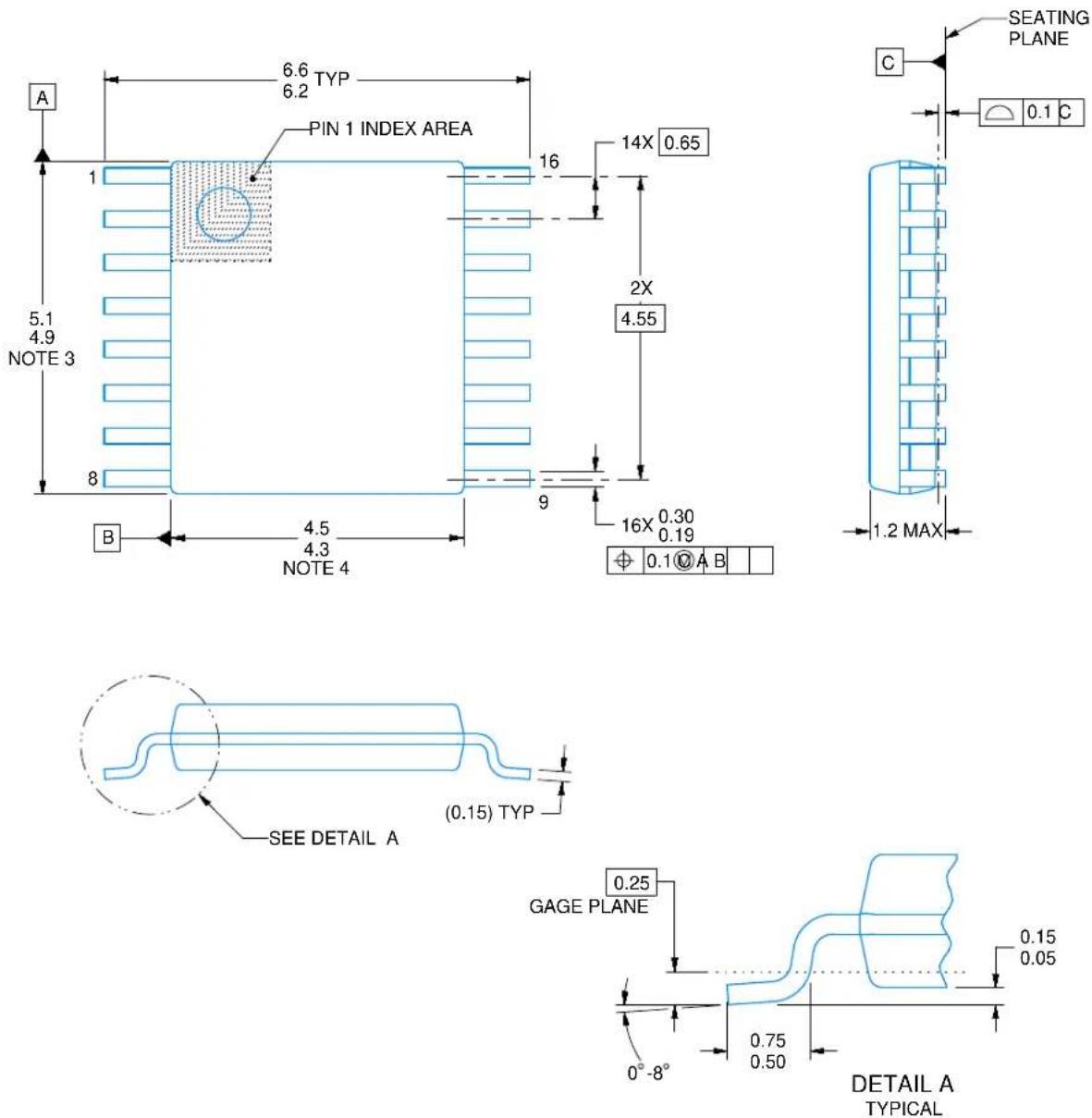
DGV (R-PDSO-G\*\*) PLASTIC SMALL-OUTLINE
24 PINS SHOWN
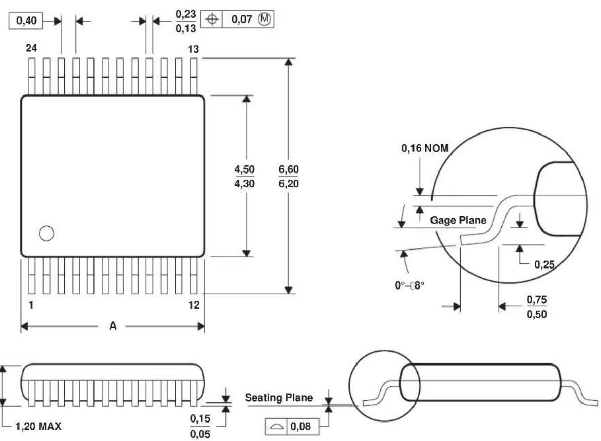
| DIM\PINS ** | 14 | 20 | 382416 | 48 | 56 | ||
| A MAX | 3,70 | 5,10 | 5,103,70 | 7,90 | 9,80 | 11,40 | |
| A MIN | 3,50 | 3,50 | 4,90 | 4,90 | 7,70 | 9,60 | 11,20 |
4073251/E 08/00
NOTES: A. All linear dimensions are in millimeters.
B. This drawing is subject to change without notice.
C. Body dimensions do not include mold flash or protrusion, not to exceed 0.15 per side.
D. Falls within JEDEC: 24/48 Pins - MO-153
14/16/20/56 Pins - MO-194
RGY (R-PVQFN-N16)
PLASTIC QUAD FLATPACK NO-LEAD
text_image
4,15 3,85 A B 15 10 16 9 3,65 3,35 1 2 7 Pin 1 Index Area Top and Bottom F 1,00 0,80 0,08 C 0,20 Nominal Lead Frame Seating Plane C 0,05 0,00 Seating Height 2,50 0,50 2 7 16X 0,50 0,30 1 1,50 THERMAL PAD 8 SIZE AND SHAPE SHOWN ON SEPRATE SHEET 9 16X 0,30 0,18 15 10 Φ 0,10 M C A B 0,05 M CBottom View
4203539-3/1 06/2011
NOTES: A. All linear dimensions are in millimeters. Dimensioning and tolerancing per ASME Y14.5M-1994.
B. This drawing is subject to change without notice.
C. QFN (Quad Flatpack No-Lead) package configuration.
D. The package thermal pad must be soldered to the board for thermal and mechanical performance.
E. See the additional figure in the Product Data Sheet for details regarding the exposed thermal pad features and dimensions.
Pin 1 identifiers are located on both top and bottom of the package and within the zone indicated.
The Pin 1 identifiers are either a molded, marked, or metal feature.
G. Package complies to JEDEC MO-241 variation BA.
RGY (R-PVQFN-N16)
PLASTIC QUAD FLATPACK NO-LEAD
THERMAL INFORMATION
This package incorporates an exposed thermal pad that is designed to be attached directly to an external heatsink. The thermal pad must be soldered directly to the printed circuit board (PCB). After soldering, the PCB can be used as a heatsink. In addition, through the use of thermal vias, the thermal pad can be attached directly to the appropriate copper plane shown in the electrical schematic for the device, or alternatively, can be attached to a special heatsink structure designed into the PCB. This design optimizes the heat transfer from the integrated circuit (IC).
For information on the Quad Flatpack No-Lead (QFN) package and its advantages, refer to Application Report, QFN/SON PCB Attachment, Texas Instruments Literature No. SLUA271. This document is available at www.ti.com.
The exposed thermal pad dimensions for this package are shown in the following illustration.
text_image
2 7 Exposed Thermal Pad 1 8 2,05±0,10 16 9 15 10 2,55±0,10 Bottom ViewExposed Thermal Pad Dimensions
4206353-3/P 03/14
NOTE: All linear dimensions are in millimeters
RGY (R-PVQFN-N16)
PLASTIC QUAD FLATPACK NO-LEAD
text_image
Example Board Layout 4,80 Note D 4,30 2,60 1,50 2,05 0,85 x 16 PL 10x0,50 0,28 x 16 PL Non Solder Mask Defined Pad R0,14 0,07 All Around Example Solder Mask Opening (Note F) 0,85 0,28 Example Pad Geometry (Note C) Example Stencil Design 0.125mm Stencil Thickness (Note E) 4,75 4,25 2,65 1,50 1,07 0,30 x 2 PL 0,82 1,07 0,80 x 16 PL 10x0,50 0,23 x 16 PL 67% solder coverage by printed area on center thermal pad Example Via Layout Design may vary depending on constraints (Note D, F) 6xØ0,3 4208122-3/P 03/14NOTES: A. All linear dimensions are in millimeters.
B. This drawing is subject to change without notice.
C. Publication IPC-7351 is recommended for alternate designs.
D. This package is designed to be soldered to a thermal pad on the board. Refer to Application Note, Quad Flat-Pack QFN/SON PCB Attachment, Texas Instruments Literature No. SLUA271, and also the Product Data Sheets for specific thermal information, via requirements, and recommended board layout. These documents are available at www.ti.com http://www.ti.com.
E. Laser cutting apertures with trapezoidal walls and also rounding corners will offer better paste release. Customers should contact their board assembly site for stencil design recommendations. Refer to IPC 7525 for stencil design considerations.
F. Customers should contact their board fabrication site for minimum solder mask web tolerances between signal pads.
SHRINK SMALL-OUTLINE PACKAGE
text_image
TYP.-244.228 -6.195.80[] PIN 1 ID AREA 16 14X .0250 [0.635] 16X -.012.008 -0.300.21[] NOTE 3 -.197.189 -5.004.81[] NOTE 4 B 8 9 2X .175 [4.45] 16X -.012.008 -0.300.21[] ⊕ .007 [0.17]@ A B S S SEATING PLANE .004 [0.1] C .069 MAX [1.75] TYP.-010.005 -0.250.13[] SEE DETAIL A .010 [0.25] GAGE PLANE 0° - 8° -.035.016 -0.880.41[] (.041) [1.04] -.010.004 -0.250.11[] DETAIL A TYPICAL 4214846/A 03/2014NOTES:
1. Linear dimensions are in inches [millimeters]. Dimensions in parenthesis are for reference only. Controlling dimensions are in inches. Dimensioning and tolerancing per ASME Y14.5M.
2. This drawing is subject to change without notice.
3. This dimension does not include mold flash, protrusions, or gate burrs. Mold flash, protrusions, or gate burrs shall not exceed .006 inch, per side.
4. This dimension does not include interlead flash.
5. Reference JEDEC registration MO-137, variation AB.
SHRINK SMALL-OUTLINE PACKAGE

text_image
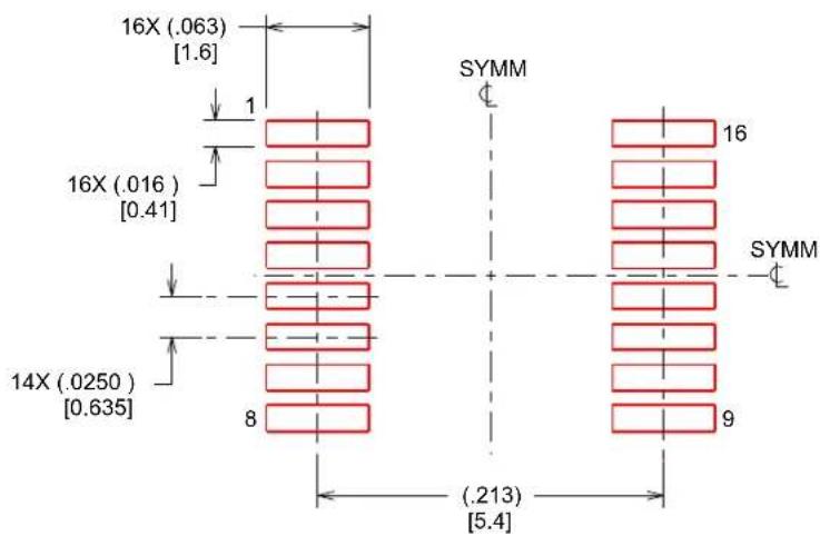
16X (.063) [1.6] 1 16X (.016) [0.41] 14X (.0250) [0.635] 8 SYM SEE DETAILS 16 9 (.213) [5.4]LAND PATTERN EXAMPLE SCALE:8X
text_image
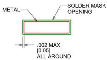
METAL SOLDER MASK OPENING .002 MAX [0.05] ALL AROUNDNON SOLDER MASK DEFINED

text_image
SOLDER MASK OPENING METAL .002 MIN [0.05] ALL AROUNDSOLDER MASK
DEFINED
SOLDER MASK DETAILS
4214846/A 03/2014
NOTES: (continued)
- Publication IPC-7351 may have alternate designs.
- Solder mask tolerances between and around signal pads can vary based on board fabrication site.
SHRINK SMALL-OUTLINE PACKAGE
other
| Dimension | Value | | --------- | ----- | | Top Section | 16X (.063) [1.6] | | Middle Section | 16X (.016) [0.41] | | Bottom Section | 14X (.0250) [0.635] | | Right Section | 16 (SYMM) | | Bottom Section | 9 (SYMM) | | Center Line Reference | (.213) [5.4] |SOLDER PASTE EXAMPLE BASED ON .005 INCH [0.127 MM] THICK STENCIL SCALE:8X
4214846/A 03/2014
NOTES: (continued)
- Laser cutting apertures with trapezoidal walls and rounded corners may offer better paste release. IPC-7525 may have alternate design recommendations.
- Board assembly site may have different recommendations for stencil design.
SMALL OUTLINE PACKAGE
4220204/A 02/2017
NOTES:
- All linear dimensions are in millimeters. Any dimensions in parenthesis are for reference only. Dimensioning and tolerancing per ASME Y14.5M.
- This drawing is subject to change without notice.
- This dimension does not include mold flash, protrusions, or gate burrs. Mold flash, protrusions, or gate burrs shall not exceed 0.15 mm per side.
- This dimension does not include interlead flash. Interlead flash shall not exceed 0.25 mm per side.
- Reference JEDEC registration MO-153.
SMALL OUTLINE PACKAGE
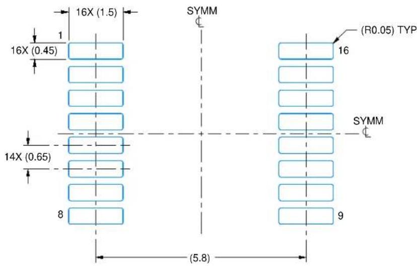
text_image
16X (1.5) 1 16X (0.45) 14X (0.65) 8 (5.8) SYMM (R0.05) TYP 16 SYMM 9LAND PATTERN EXAMPLE
EXPOSED METAL SHOWN
SCALE: 10X

text_image
SOLDER MASK OPENING METAL EXPOSED METAL 0.05 MAX ALL AROUNDNON-SOLDER MASK DEFINED (PREFERRED)

text_image
METAL UNDER SOLDER MASK SOLDER MASK OPENING EXPOSED METAL 0.05 MIN ALL AROUNDSOLDER MASK
DEFINED
SOLDER MASK DETAILS
4220204/A 02/2017
NOTES: (continued)
- Publication IPC-7351 may have alternate designs.
- Solder mask tolerances between and around signal pads can vary based on board fabrication site.
SMALL OUTLINE PACKAGE

text_image
16X (1.5) 1 16X (0.45) SYMM (R0.05) TYP 16 14X (0.65) 8 (5.8) 9 SYMMSOLDER PASTE EXAMPLE
BASED ON 0.125 mm THICK STENCIL
SCALE: 10X
4220204/A 02/2017
NOTES: (continued)
- Laser cutting apertures with trapezoidal walls and rounded corners may offer better paste release. IPC-7525 may have alternate design recommendations.
- Board assembly site may have different recommendations for stencil design.
IMPORTANT NOTICE AND DISCLAIMER
TI PROVIDES TECHNICAL AND RELIABILITY DATA (INCLUDING DATA SHEETS), DESIGN RESOURCES (INCLUDING REFERENCE DESIGNS), APPLICATION OR OTHER DESIGN ADVICE, WEB TOOLS, SAFETY INFORMATION, AND OTHER RESOURCES "AS IS" AND WITH ALL FAULTS, AND DISCLAIMS ALL WARRANTIES, EXPRESS AND IMPLIED, INCLUDING WITHOUT LIMITATION ANY IMPLIED WARRANTIES OF MERCHANTABILITY, FITNESS FOR A PARTICULAR PURPOSE OR NON-INFRINGEMENT OF THIRD PARTY INTELLECTUAL PROPERTY RIGHTS.
These resources are intended for skilled developers designing with TI products. You are solely responsible for (1) selecting the appropriate TI products for your application, (2) designing, validating and testing your application, and (3) ensuring your application meets applicable standards, and any other safety, security, regulatory or other requirements.
These resources are subject to change without notice. TI grants you permission to use these resources only for development of an application that uses the TI products described in the resource. Other reproduction and display of these resources is prohibited. No license is granted to any other TI intellectual property right or to any third party intellectual property right. TI disclaims responsibility for, and you will fully indemnify TI and its representatives against, any claims, damages, costs, losses, and liabilities arising out of your use of these resources.
TI's products are provided subject to TI's Terms of Sale or other applicable terms available either on ti.com or provided in conjunction with such TI products. TI's provision of these resources does not expand or otherwise alter TI's applicable warranties or warranty disclaimers for TI products.
TI objects to and rejects any additional or different terms you may have proposed.
Mailing Address: Texas Instruments, Post Office Box 655303, Dallas, Texas 75265
Copyright © 2022, Texas Instruments Incorporated