TL064BCN - Electronic component TEXAS INSTRUMENTS - Free user manual and instructions
Find the device manual for free TL064BCN TEXAS INSTRUMENTS in PDF.

User questions about TL064BCN TEXAS INSTRUMENTS
0 question about this device. Answer the ones you know or ask your own.
Ask a new question about this device
Download the instructions for your Electronic component in PDF format for free! Find your manual TL064BCN - TEXAS INSTRUMENTS and take your electronic device back in hand. On this page are published all the documents necessary for the use of your device. TL064BCN by TEXAS INSTRUMENTS.
USER MANUAL TL064BCN TEXAS INSTRUMENTS
TL06xxLow-PowerJFET-InputOperationalAmplifiers
1Features2Applications
•VeryLowPowerConsumption
•TypicalSupplyCurrent:200μA(PerAmplifier)•Whitegoods
- WideCommon-ModeandDifferentialVoltage-Personalelectronics Ranges
- Con
- LowInputBiasandOffsetCurrents
- Common-ModelInputVoltageRange IncludesV CC+
•OutputShort-CircuitProtection
•HighInputImpedance:JFET-InputStage
- InternalFrequencyCompensation
- Latch-Up-FreeOperation
•HighSlewRate:3.5V/μsTypical
- OnProductsComplianttoMIL-PRF-38535, AllParametersAreTestedUnlessOtherwise Noted.OnAllOtherProducts,Production ProcessingDoesNotNecessarilyIncludeTesting ofAllParameters.
- Tablets
•Computers
3Description
The JFET-inputoperational amplifiers of the TL06x series are designed as low-power versions of the TL08x series amplifiers. They feature high input impedance, wide bandwidth, high slew rate, and low input offset and input bias currents. The TL06x series feature the sameterminal assignments as the TL07x and TL08x series.
DeviceInformation (1)
| PART NUMBER | PACKAGE | BODY SIZE (NOM) |
| TL06xxD | SOIC (14) | 8.65 mm × 3.91 mm |
| TL06xxJ | CDIP (14) | 19.56 mm × 6.92 mm |
| TL06xxN | PDIP (14) | 19.30 mm × 6.35 mm |
| TL06xxNS | SO (14) | 10.30 mm × 5.30 mm |
| TL06xxPW | TSSOP (14) | 5.00 mm × 4.40 mm |
(1) For all available packages, see the orderable addendum at the end of the data sheet.

flowchart
graph TD
    A["IN+"] --> B["+"]
    C["IN-"] --> B
    B --> D["OUT"]
    E["OFFSET N1"] --> F["OFFSET N2"]
    G["Offset Null/Compensation TL061 Only"] --> H["Ground"]
TableofContents
1 Features.... 1
2 Applications 1
3 Description 1
4 Revision History...... 2
5PinConfigurationandFunctions....3
6 Specifications.... 4
6.1 AbsoluteMaximumRatings....4
6.2ESDRatings....5
6.3RecommendedOperatingConditions....5
6.4ThermalInformation-8Pins....5
6.5ThermalInformation-14Pins....5
6.6ThermalInformation-20Pins....6
6.7 Electrical Characteristics for TL06xCandTL06xxC.6
6.8 Electrical Characteristics for TL06xxCandTL06xl...7
6.9 Electrical Characteristics for TL06xM and TL064M..7
6.10 Operating Characteristics....8
6.11 TypicalCharacteristics....9
7ParameterMeasurementInformation....13
8DetailedDescription....14
8.1Overview....14
8.2FunctionalBlockDiagram....14
8.3FeatureDescription....14
8.4DeviceFunctionalModes....15
9ApplicationsandImplementation....16
9.1 Application Information....16
9.2TypicalApplications....16
9.3SystemExamples....17
10PowerSupplyRecommendations....19
11 Layout.... 20
11.1 LayoutGuidelines....20
11.2LayoutExamples....20
12DeviceandDocumentationSupport....21
12.1 DocumentationSupport....21
12.2RelatedLinks....21
12.3CommunityResources....21
12.4Trademarks....21
12.5ElectrostaticDischargeCaution....21
12.6Glossary....21
13Mechanical, Packaging, and Orderable Information 21
4RevisionHistory
NOTE: Pagenumbersforpreviousrevisionsmaydifferfrompagenumbersinthecurrentversion.
ChangesfromRevisionK(January2014)toRevisionLPage
- Added Applications.... 1
- Added Pin Configuration and Functions section, ESD Ratings table, Feature Description section, Device Functional Modes, Application and Implementation section, Power Supply Recommendations section, Layout section, Device and Documentation Support section, and Mechanical, Packaging, and Orderable Information section .... 1
ChangesfromRevisionJ(September2004)toRevisionK
Page
- Updated document to new TI data sheet format - no specification changes. 1
- Deleted Ordering Information table. 1
- Updated Features with Military Disclaimer.... 1
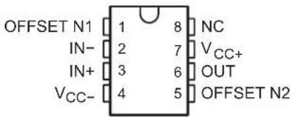
5PinConfigurationandFunctions
TL061xD,P,andPSPackage
8-PinSOIC, PDIP, and SO TopView
text_image
OFFSET N1 1 8 NC IN- 2 7 VCC+ IN+ 3 6 OUT VCC- 4 5 OFFSET N2TL062xD,JG,P,PS,andPWPackage
B-PinSOIC,CDIP,PDIP,SO,andTSSO
TopView

text_image
1OUT 1 8 VCC+ 1IN- 2 7 2OUT 1IN+ 3 6 2IN- VCC- 4 5 2IN+TL064xD,J,N,NS,PW,andWPackage
14-PinSOIC,CDIP,PDIP,SO,TSSOPandCFP
TopView
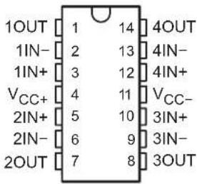
text_image
1OUT 1 14 4OUT 1IN- 2 13 4IN- 1IN+ 3 12 4IN+ VCC+ 4 11 VCC- 2IN+ 5 10 3IN+ 2IN- 6 9 3IN- 2OUT 7 8 3OUTTL062FKPackage
20-PinLCCC
TopView
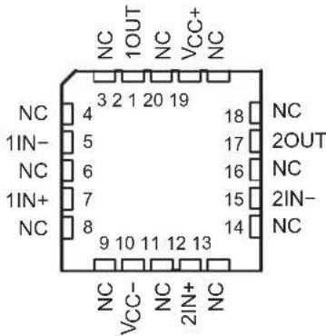
text_image
NC 1OUT NC VCC+ NC NC 4 3 2 1 20 19 1IN- 5 NC 6 1IN+ 7 NC 8 9 10 11 12 13 VCC- NC 2OUT NC 16 15 14 2IN- NCTL064FKPackage
20-PinLCCC
TopView
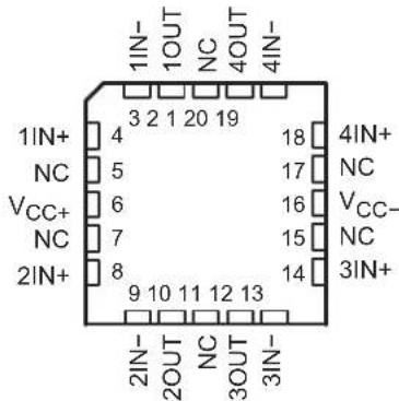
text_image
1IN- 1OUT NC 4OUT 4IN- 3 2 1 20 19 1IN+ 4 NC VCC+ 6 NC 2IN+ 8 9 10 11 12 13 2IN- 2OUT NC 3OUT 3IN- 18 4IN+ 17 NC VCC- 16 NC 15 3IN+PinFunctions
| PIN | TYPE | DESCRIPTION | |||||
| NAME | TL061TL062 | TL064 | |||||
| D,P,PS | D,JG,P, PS,PW | FK | D,J,N,NS, PW,W | FK | |||
| 1IN- | — | 2 | 5 | 2 | 3 | I | Negative input |
| 1IN+ | — | 3 | 7 | 3 | 4 | I | Positive input |
| 1OUT | — | 1 | 2 | 1 | 2 | O | Output |
| 2IN- | — | 6 | 15 | 6 | 9 | I | Negative input |
| 2IN+ | — | 5 | 12 | 5 | 8 | I | Positive input |
| 2OUT | — | 7 | 17 | 7 | 10 | O | Output |
| 3IN- | — | — | — | 9 | 13 | I | Negative input |
| 3IN+ | — | — | — | 10 | 14 | I | Positive input |
| 3OUT | — | — | — | 8 | 12 | O | Output |
| 4IN- | — | — | — | 13 | 19 | I | Negative input |
| 4IN+ | — | — | — | 12 | 18 | I | Positive input |
| 4OUT | — | — | — | 14 | 20 | O | Output |
| IN- | 2 | — | — | — | — | I | Negative input |
PinFunctions(continued)
| PIN | TYPEDESCRIPTION | |||||
| NAME | TL061TL062TL064 | |||||
| D,P,PSFKFK | D,JG,P,D,JPS,PWPW,W | N,NS, W | ||||
| IN+3—— | I | Positiveinput | ||||
| NC | 8 | — | 1 | — | 1 | — |
| 3 | ||||||
| 4 | 5 | |||||
| 6 | ||||||
| 8 | 7 | |||||
| 9 | ||||||
| 11 | 11 | |||||
| 13 | ||||||
| 14 | 15 | |||||
| 16 | ||||||
| 18 | 17 | |||||
| 19 | ||||||
| OFFSET N1 | 1 | — | — | — | — | — |
| OFFSET N2 | 5 | — | — | — | — | — |
| OUT | 6—— | O | Output | |||
| V_CC- | 4 | 4 | 10 | 11 | 16 | — |
| V_CC+ | 7 | 8 | 20 | 4 | 6 | — |
6 Specifications
6.1 Absolute Maximum Ratings
over operating free-air temperature range (unless otherwise noted) ^(1)
| MINMAX | UNIT | |||
| V_CC+ | Supplyvoltage (2) | 18 | V | |
| V_CC- | -18 | |||
| V_ID | Differentialinputvoltage (3) | ±30 | V | |
| V_I | Inputvoltage (2)(4) | ±15 | V | |
| Durationofoutputshortcircuit (5) | Unlimited | |||
| T_J | Operatingvirtualjunctiontemperature | 150 | °C | |
| Casetemperaturefor60secondsFKpackage | 260 | °C | ||
| Leadtemperature1.6mm(1/16inch)from casefor60seconds | J,JG,U,orWpackage | 300 | °C | |
| Leadtemperature1.6mm(1/16inch)from casefor10seconds | D,N,NS,P,PS,orPWpackage | 260 | °C | |
| T_stg | Storagetemperature | -65 | 150 | °C |
(1) Stresses beyond those listed under Absolute Maximum Ratings may cause permanent damage to the device. These are stress ratings only, and functional operation of the device at these or any other conditions beyond those indicated under Recommended Operating Conditions is not implied. Exposure to absolute-maximum-rated conditions for extended periods may affect device reliability.
(2) All voltage values, except differential voltages, are with respect to the midpoint between V_CC+ and V_CC- .
(3) DifferentialvoltagesareatIN+, withrespecttolN-.
(4) The magnitude of the input voltage must never exceed the magnitude of the supply voltage or 15 V, whichever is less.
(5) The output may be shorted to ground or to either supply. Temperature and/or supply voltages must be limited to ensure that the dissipation rating is not exceeded.
6.2ESDRatings
| VALUEUNIT | |||
| V_(ESD) ElectrostaticdischargeV | Humanbodymodel(HBM),perANSI/ESDA/JEDECJS-001 (1) | 2000 | |
| Charged-devicemodel(CDM),perJEDECspecificationJESD22-C101(2) | 2000 | ||
(1)JEDECdocumentJEP155statesthat500-VHBMallowssafemanufacturingwithastandardESDcontrolprocess.
(2)JEDECdocumentJEP157statesthat250-VCDMallowssafemanufacturingwithastandardESDcontrolprocess.
6.3 Recommended Operating Conditions
overoperatingfree-airtemperaturerange(unlessotherwisenoted)
| MINMAXUNIT | ||||
| V_CC+ Supplyvoltage515V | ||||
| V_CC- Supplyvoltage-5 -15V | ||||
| V_CM Common-modevoltage | V_CC- +4 V_CC+ -4 | V | ||
| T_A Ambienttemperature | TL06xM | -55 125 | °C | |
| TL06xQ | -40 125 | |||
| TL06xI | -4085 | |||
| TL06xC | 070 | |||
6.4ThermalInformation-8Pins
| THERMALMETRIC (1) | TL06xx | UNIT | ||||
| D (SOIC) | P (PDIP) | PS (SO) | PW (TSSOP) | JG (CDIP) | ||
| 8 PINS | 8 PINS | 8 PINS | 8 PINS | 8 PINS | ||
| R_ J Junction-to-ambientthermal resistance(2)(3) | 97 | 85 | 95 | 149 | — | °C/W |
| R_ J Junction-to-case(top)thermal resistance(4)(5)p) | — | — | — | — | 14.5 | °C/W |
(1) For more information about traditional and new thermal metrics, see the Semiconductor and IC Package Thermal Metrics application report, SPRA953.
(2)MaximumpowerdissipationisafunctionofT J() , R_ JA , and T A. The maximum allowable powerdissipation at any allowable ambient temperature is P_D = (T_J() - T_A) / R_ JA . Operating at the absolute maximum T of 150°C can affect reliability.
(3) The packagethermalimpedance is calculated in accordance with JESD51-7.
(4) Maximum power dissipation is a function of T J_(max) , R JC , and T C . The maximum allowable power dissipation at any allowable ambient temperature is P D = (TJ(max) - T_C)/R_ JC . Operating at the absolute maximum T J of 150°C can affect reliability.
(5) The packagethermalimpedance is calculated in accordance with MIL-STD-883.
6.5ThermalInformation-14Pins
| THERMALMETRIC (1) | TL06xx | UNIT | |||||||
| D (SOIC) | N (PDIP) | NS (SO) | PS (SO) | PW (TSSOP) | J (CDIP) | W (CFP) | |||
| 14 PINS | 14 PINS | 14 PINS | 8 PINS | 14 PINS | 14 PINS | 14 PINS | |||
| R_ J A | Junction-to-ambientthermal resistance(2)(3) | 86 | 80 | 76 | 95 | 113 | — | — | °C/W |
| R_ J C(top p) | Junction-to-case(top)thermal resistance(2)(3) | — | — | — | — | — | 15.05 | 14.65 | °C/W |
(1) For more information about traditional and new thermal metrics, see the Semiconductor and IC Package Thermal Metrics application report, SPRA953.
(2)MaximumpowerdissipationisafunctionofT J_(max) , R_ JC , and T C . The maximumallowablepowerdissipationatanyallowableambient temperatureisP D = (TJ(max) - T_C)/R_ JC . Operating at the absolute maximum T _J of 150°C can affect reliability.
(3) The packagethermal impedance is calculated in accordance with MIL-STD-883.
6.6ThermalInformation-20Pins
| THERMALMETRIC (1) | TL06xx | ||
| FK(LCCC)UNIT | |||
| 20PINS | |||
| R_ JA | Junction-to-ambientthermalresistance (2)(3) | —°C/W | |
| R_ JC(top) | Junction-to-case(top)thermalresistance (4)(5) | 5.61°C/W | |
(1) For more information about traditional and new thermal metrics, see the Semiconductor and IC Package Thermal Metrics application report, SPRA953.
(2)MaximumpowerdissipationisafunctionofT J() , R J A , and T A . The maximumallowablepowerdissipationatanyallowableambient temperatureisP D = (T_J() - T_A) / R_ J A . OperatingattheabsolutemaximumT J of 150°C canaffectreliability.
(3) The packagethermalimpedance is calculated in accordance with JESD51-7.
(4)MaximumpowerdissipationisafunctionofT J() , R_ JC , and T C . The maximumallowablepowerdissipationatanyallowableambient temperatureisP D = (T_J() - T_C)/R_ JC . Operating at the absolute maximum T _J of 150°C can affect reliability.
(5) The packagethermalimpedance is calculated in accordance with MIL-STD-883.
6.7 Electrical Characteristics for TL06xCand TL06xxC
V_CC±=±15V(unlessotherwisenoted)
| PARAMETERTESTCONDITIONS | (1) | TL061C,TL062C,TL064C | TL061AC,TL062AC,TL064AC | UNIT | ||||
| MINTYPMAXMINTYPMAX | ||||||||
| V_IO | Inputoffsetvoltage | V_O=0,R_S=50Ω | T_A=25°C3 | 15 | 3 | 6 | mV | |
| T_A=Fullrange | 20 | 7.5 | ||||||
| _VIO | Temperaturecoefficient ofinputoffsetvoltage | V_O=0,R_S=50Ω,T_A=Full range | 10 | 10 | μV/°C | |||
| I_IO | Inputoffsetcurrent | V_O=0 | T_A=25°C | 5 200 | 5 100 | pA | ||
| T_A=Fullrange | 5 | 3 | nA | |||||
| I_IB | Inputbiascurrent (2) | V_O=0 | T_A=25°C | 30 400 | 30 200 | pA | ||
| T_A=Fullrange | 10 | 7 | nA | |||||
| V_ICR | Common-modeinput voltagerrange | T_A=25°C | -12±11 to 15 | -12±11 to 15 | V | |||
| V_OM | Maximumppeakoutput voltageswing | R_L=10kΩ,T_A=25°C | ±10 ±13.5±10 ±13.5 | V | ||||
| R_L≥10kΩ,T_A=Fullrange | ±10 | ±10 | ||||||
| A_VD | Large-signaldifferential voltageamplification | V_O=±10V,R_L≥2kΩ | T_A=25°C3 | 6 | 4 | 6 | V/mV | |
| T_A=Fullrange | 3 | 4 | ||||||
| B_1 | Unity-gainbandwidth | R_L=10kΩ,T_A=25°C | 1 | 1 | MHz | |||
| r_i | Inputresistance | T_A=25°C | 10^12 | 10^12 | Ω | |||
| CMRR | Common-mode rejection ratio | V_IC=V_ICRmin,V_O=0,R_S=50Ω,T_A=25°C | 70 | 86 | 80 | 86 | dB | |
| k_SVR | Supply-voltage rejection ratio ( V_CC/ V_IO ) | V_CC=±9Vto±15V,V_O=0,R_S=50Ω,T_A=25°C | 70 | 95 | 80 | 95 | dB | |
| P_D | Totalpowerdissipation (eachamplifier) | V_O=0,Noload,T_A=25°C | 6 7.5 | 6 7.5 | mW | |||
| I_CC | Supplycurrent (eachamplifier) | V_O=0,Noload,T_A=25°C | 200 250 | 200 250 | μA | |||
| V_O1/V_O2 | Crosstalkattenuation | A_VD=100,T_A=25°C | 120 | 120 | dB | |||
(1) All characteristics are measured under open-loop conditions with zero common-mode input voltage unless otherwise specified. Full rangeforT _A is0°C to 70°C for TL06xC, TL06xAC, and TL06xBC and -40°C to 85°C for TL06xI.
(2) Input bias currents of an FET-input operational amplifier are normal junction reverse currents, which are temperature sensitive, as shown in Figure 12. Pulse techniques are used to maintain the junction temperature as close to the ambient temperature as possible.
6.8 Electrical Characteristics for TL06xxCandTL06xl
V_CC± = ± 15V(unless otherwise noted)
| PARAMETERTESTCONDITIONS | (1) | TL061BC,TL062BC,TL064BC | TL061I,TL062I,TL064I | UNIT | ||||
| MINTYPMAXMINTYPMAX | ||||||||
| V_IO | InputoffsetvoltageV | O=0,R_S=50Ω | T_A=25°C2336 | |||||
| T_A=Fullrange5 | 9 | |||||||
| _VIO | Temperaturecoefficient ofinputoffsetvoltage | V_O=0,R_S=50Ω,T_A=Full range | 10 | 10 | μV/°C | |||
| I_IO | InputoffsetcurrentV | O=0 | T_A=25°C5 1005 100 pA | |||||
| T_A=Fullrange3 | 10 | nA | ||||||
| I_IB | Inputbiascurrent (2) | V_O=0 | T_A=25°C | 30 200 | 30 200 | pA | ||
| T_A=Fullrange7 | 20 | nA | ||||||
| V_ICR | Common-modeinput voltage range | T_A=25°C | -12±11 to15 | -12±11 to15 | V | |||
| V_OM | Maximumpeakoutput voltageswing | R_L=10kΩ,T_A=25°C | ±10 ±13.5 | ±10 ±13.5 | V | |||
| R_L≥10kΩ,T_A=Full range | ±10 | ±10 | ||||||
| A_VD | Large-signal differential voltage amplification | V_O=±10V,R_L≥2kΩ | T_A=25°C | 4646 | V/mV | |||
| T_A=Full range | 4 | 4 | ||||||
| B_1 | Unity-gainbandwidth | R_L=10kΩ,T_A=25°C | 1 | 1 | MHz | |||
| r_I | Inputresistance | T_A=25°C | 10^12 | 10^12 | Ω | |||
| CMRR | Common-mode rejection ratio | V_IC=V_ICRmin,V_O=0,R_S=50Ω,T_A=25°C | 80 86 | 80 86 | dB | |||
| k_SVR | Supply-voltage rejection ratio ( V_CC/ V_IO ) | V_CC=±9Vto±15V,V_O=0,R_S=50Ω,T_A=25°C | 80 95 | 80 95 | dB | |||
| P_D | Total power dissipation (each amplifier) | V_O=0,Noload,T_A=25°C | 6 7.5 | 6 7.5 | mW | |||
| I_CC | Supply current (each amplifier) | V_O=0,Noload,T_A=25°C | 200 250 | 200 250 | μA | |||
| V_D1/V_O2 | Crosstalkattenuation | A_VD=100,T_A=25°C | 120 | 120 | dB | |||
(1) All characteristics are measured under open-loop conditions with zero common-mode input voltage, unless otherwise specified. Full range for T_A is 0°C to 70°C for TL06xC, TL06xAC, and TL06xBC and -40°C to 85°C for TL06xl.
(2) Input bias currents of an FET-input operational amplifier are normal junction reverse currents, which are temperature sensitive, as shown in Figure 12. Pulse techniques are used to maintain the junction temperature as close to the ambient temperature as possible.
6.9 Electrical Characteristics for TL06xM and TL064M
V_CC± = ± 15V (unless otherwise noted)
| PARAMETERTESTCONDITIONS | (1) | TL061M,TL062M | TL064M | UNIT | |||||
| MINTYPMAXMINTYPMAX | |||||||||
| V_IO | InputoffsetvoltageV | O=0,R_S=50Ω | T_A=25°C3639 | ||||||
| mY_A=-55°Cto 125°C | 9 | 15 | |||||||
| _VIO | Temperaturecoefficient ofinputoffsetvoltage | V_O=0,R_S=50Ω,T_A=-55°Cto125°C | 10 | 10 | μV/°C | ||||
| I_IO | InputoffsetcurrentV | O=0 | T_A=25°C5 | 1005 | 100 | pA | |||
| T_A=-55°C | 20(2) | 20(2) | nA | ||||||
| T_A=125°C | 20 | 20 | |||||||
| I_IB | Inputbiascurrent (3) | V_O=0 | T_A=25°C | 30 | 200 | 30 | 200 | pA | |
| T_A=-55°C | 50(2) | 50(2) | nA | ||||||
| T_A=125°C | 50 | 50 | |||||||
| V_ICR | Common-modeinput voltagerange | T_A=25°C | ±11 | -12 to 15 | ±11 | -12 to 15 | V | ||
(1) All characteristics are measured under open-loop conditions, with zero common-mode voltage, unless otherwise specified.
(2) This parameter is not production tested.
(3) Input bias currents of an FET-input operational amplifier are normal junction reverse currents, which are temperature sensitive, as shown in Figure 12. Pulse techniques are used to maintain the junction temperature as close to the ambient temperature as possible.
ElectricalCharacteristicsforTL06xMandTL064M(continued)
V_CC± = ± 15V(unless otherwise noted)
| PARAMETERTESTCONDITIONS | (1) | TL061M,TL062MTL064M | UNIT | |||||
| MINTYPMAXMINTYPMAX | ||||||||
| V_OM | Maximumppeakoutput voltageswing | R_L=10kΩ,T_A=25°C±10±13.5±10±13.5 | V | |||||
| R_L≥ 10kΩ,T_A=-55°Cto125°C±10±10 | ||||||||
| A_VD | Large-signaldifferential voltageamplification | V_O=±10V,R_L≥ 2kΩ | T_A=25°C46 | 46 | V/mV | |||
| T_A=-55°Cto125°C | 4 | 4 | ||||||
| B_1 | Unity-gainbandwidth | R_L=10kΩ,T_A=25°C | MHz | |||||
| r_i | Inputresistance | T_A=25°C | 10^12 | 10^12 | Ω | |||
| CMRR | Common-mode rejection ratio | V_IC=V_ICRmin,V_O=0,R_S=50Ω,T_A=25°C | 80 86 | 80 86 | dB | |||
| k_SVR | Supply-voltage rejection ratio ( V_CC/ V_IO ) | V_CC=±9Vto±15V,V_O=0,R_S=50Ω,T_A=25°C | 80 95 | 80 95 | dB | |||
| P_D | Totalpowerdissipation (eachamplifier) | V_O=0,Noload,T_A=25°C | 6 7.5 | 6 7.5 | mW | |||
| I_CC | Supplycurrent (eachamplifier) | V_O=0,Noload,T_A=25°C | 200 250 | 200 250 | μA | |||
| V_D1/V_O2 | Crosstalkattenuation | A_VD=100,T_A=25°C | 120120 | dB | ||||
6.10 OperatingCharacteristics
V_CC±=±15V,T A=25°C
| PARAMETER | TEST CONDITIONS | MIN | TYP | MAX | UNIT | ||
| SR | Slew rate at unity gain (1) | V_I = 10 V, R_L = 10 k, | C_L = 100 pF, see Figure 16 | 1.53.5 | V/μs | ||
| t_r | Rise-time | V_I = 20 V, R_L = 10 k, | C_L = 100 pF, see Figure 16 | 0.2 | μs | ||
| Overshoot factor | 10% | ||||||
| V_n | Equivalent input noise voltage | R_S = 20 | f = 1 kHz | 42 | nV/ | ||
(1) Slew rate at -55^ to 125^ is 0.7 V/ s min.
6.11 Typical Characteristics
Dataathighandlowtemperaturesareapplicableonlywithinthespecifiedoperatingfree-airtemperaturerangesofthe variousdevices.
Table1.TableofGraphs
| FIGURE | |
| MaximumpeakoutputvoltageversusSupplyvoltageFigure1 | |
| MaximumpeakoutputvoltageversusFree-airtemperatureFigure2 | |
| MaximumpeakoutputvoltageversusLoadresistanceFigure3 | |
| MaximumpeakoutputvoltageversusFrequencyFigure4 | |
| DifferentialvoltageamplificationversusFree-airtemperatureFigure5 | |
| Large-signaldifferentialvoltageamplificationversusFrequencyFigure6 | |
| PhaseshiftversusFrequencyFigure6 | |
| SupplycurrentversusSupplyvoltageFigure7 | |
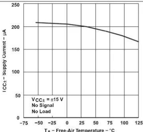
| SupplycurrentversusFree-airtemperature | Figure8 |
| TotalpowerdissipationversusFree-airtemperature | Figure9 |
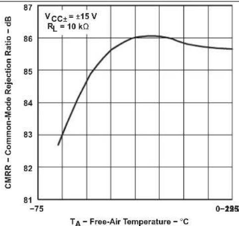
| Common-moderejectionratioversusFree-airtemperature | Figure10 |
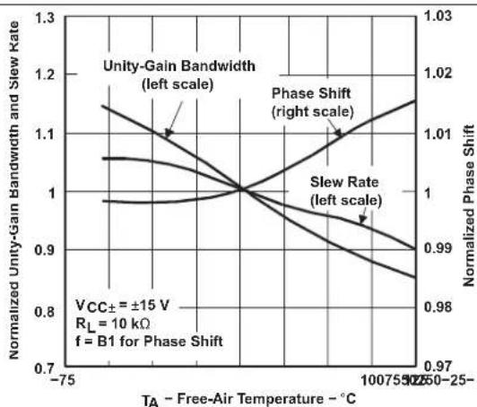
| Normalized unity-gain bandwidth versus Free-air temperature | Figure 11 |
| NormalizedslewrateversusFree-airtemperature | Figure11 |
| NormalizedphaseshiftversusFree-airtemperature | Figure11 |
| InputbiascurrentversusFree-airtemperature | Figure12 |
| Voltage-followerlarge-signalpulseresponseversusTime | Figure13 |
| OutputvoltageversusElapsedtime | Figure14 |
| EquivalentinputnoisevoltageversusFrequency | Figure15 |
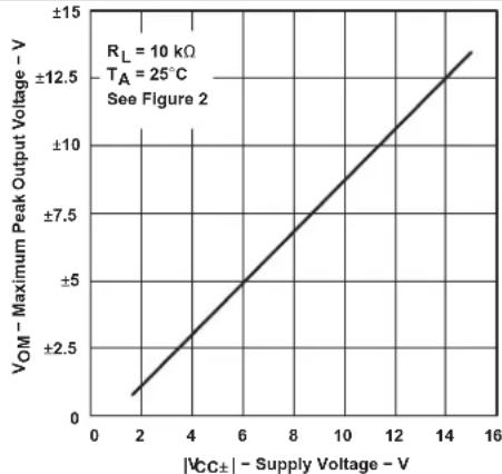
Figure 1. Maximum Peak Output Voltage vs Supply Voltage
line
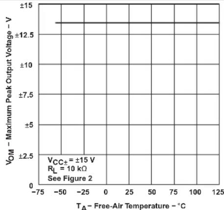
| T_A - Free-Air Temperature (°C) | V_OM - Maximum Peak Output Voltage (V) | | ------------------------------- | -------------------------------------- | | -75 | ±12.5 | | -50 | ±12.5 | | -25 | ±12.5 | | 0 | ±12.5 | | 25 | ±12.5 | | 50 | ±12.5 | | 75 | ±12.5 | | 100 | ±12.5 | | 125 | ±12.5 |Figure 2. Maximum Peak Output Voltage vs Free-Air Temperature

line
| RL - Load Resistance - Ω | VOM - Maximum Peak Output Voltage - V | | ------------------------ | ------------------------------------- | | 100 | ±15 | | 200 | 2.5 | | 400 | 5 | | 700 | 7.5 | | 1k | 10 | | 2k | 12.5 | | 4k | 13.5 | | 7k | 14 | | k | 14.5 |Figure 3. Maximum Peak Output Voltage vs Load Resistance

line
| f - Frequency - Hz | VCC± = ±5 V | VCC± = ±12 V | VCC± = ±15 V | | ------------------ | ----------- | ------------ | ------------ | | 1 k | 4.0 | 13.0 | 13.0 | | 10 k | 4.0 | 13.0 | 13.0 | | 100 k | 2.5 | 7.5 | 10.0 | | 1 M | 0.0 | 2.5 | 5.0 | | 10 M | 0.0 | 0.0 | 0.0 |Figure 4. Maximum Peak Output Voltage vs Frequency
line
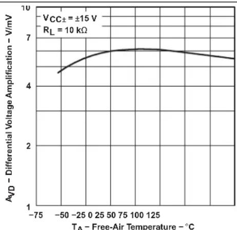
| TA - Free-Air Temperature (°C) | AVD - Differential Voltage Amplification (V/mV) | | ------------------------------ | ----------------------------------------------- | | -75 | 4.5 | | -50 | 5.0 | | -25 | 5.5 | | 0 | 6.0 | | 25 | 6.2 | | 50 | 6.3 | | 75 | 6.4 | | 100 | 6.5 | | 125 | 6.4 | | 150 | 6.3 | | 175 | 6.2 | | 200 | 6.1 | | 225 | 6.0 | | 250 | 5.9 | | 275 | 5.8 | | 300 | 5.7 | | 325 | 5.6 | | 350 | 5.5 | | 375 | 5.4 | | 400 | 5.3 | | 425 | 5.2 | | 450 | 5.1 | | 475 | 5.0 | | 500 | 4.9 | | 525 | 4.8 | | 550 | 4.7 | | 575 | 4.6 | | 600 | 4.5 | | 625 | 4.4 | | 650 | 4.3 | | 675 | 4.2 | | 700 | 4.1 | | 725 | 4.0 | | 750 | 3.9 | | 775 | 3.8 | | 800 | 3.7 | | 825 | 3.6 | | 850 | 3.5 | | 875 | 3.4 | | 900 | 3.3 | | 925 | 3.2 | | 950 | 3.1 | | 975 | 3.0 | | 1000 | 2.9 | | 1025 | 2.8 | | 1050 | 2.7 | | 1075 | 2.6 | | 1100 | 2.5 | | 1125 | 2.4 | | 1150 | 2.3 | | 1175 | 2.2 | | 1200 | 2.1 | | 1225 | 2.0 | | 1250 | 1.9 | | 1275 | 1.8 | | 1300 | 1.7 | | 1325 | 1.6 | | 1350 | 1.5 | | 1375 | 1.4 | | 1400 | 1.3 | | 1425 | 1.2 | | 1450 | 1.1 | | 1475 | 1.0 | | 1500 | 0.9 | | 1525 | 0.8 | | 1550 | 0.7 | | 1575 | 0.6 | | 1600 | 0.5 | | 1625 | 0.4 | | 1650 | 0.3 | | 1675 | 0.2 | | 1700 | 0.1 | | 1725 | 0.0 | | 1750 | -0.1 | | 1775 | -0.2 | | 1800 | -0.3 | | 1825 | -0.4 | | 1850 | -0.5 | | 1875 | -0.6 | | 1900 | -0.7 | | 1925 | -0.8 | | 1950 | -0.9 | | 1975 | -1.0 | | 2000 | -1.1 | | 2025 | -1.2 | | 2050 | -1.3 | | 2075 | -1.4 | | 2100 | -1.5 | | 2125 | -1.6 | | 2150 | -1.7 | | 2175 | -1.8 | | 2200 | -1.9 | | 2225 | -2.0 | | 2250 | -2.1 | | 2275 | -2.2 | | 2300 | -2.3 | | 2325 | -2.4 | | 2350 | -2.5 | | 2375 | -2.6 | | 2400 | -2.7 | | 2425 | -2.8 | | 2450 | -2.9 | | 2475 | -3.0 | | 2500 | -3.1 | | 2525 | -3.2 | | 2550 | -3.3 | | 2575 | -3.4 | | 2600 | -3.5 | | 2625 | -3.6 | | 2650 | -3.7 | | 2675 | -3.8 | | 2700 | -3.9 | | 2725 | -4.0 | | 2750 | -4.1 | | 2775 | -4.2 | | 2800 | -4.3 | | 2825 | -4.4 | | 2850 | -4.5 | | 2875 | -4.6 | | 2900 | -4.7 | | 2925 | -4.8 | | 2950 | -4.9 | | 2975 | -5.0 | | Note: The actual values for ΔV = VCC± and ΔV = VCL = ±15 V are not provided in the code snippet, so they are not included in the original data series in the code snippet box above it.Figure 5. Differential Voltage Amplification vs Free-Air Temperature
line
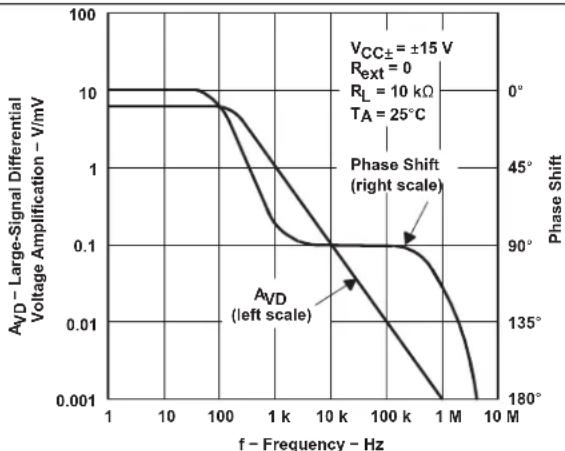
| f - Frequency - Hz | A_VD - Large-Signal Differential Voltage Amplification - V/mV | Phase Shift (right scale) | | ------------------ | ------------------------------------------------------------- | -------------------------- | | 1 | 10 | 0° | | 10 | 10 | 0° | | 100 | 10 | 45° | | 1k | 1 | 90° | | 10k | 0.1 | 135° | | 100k | 0.01 | 180° | | 1M | 0.001 | — | | 10M | — | — |Figure 6. Large-Signal Differential Voltage Amplification and Phase Shift vs Frequency

Figure 7. Supply Current vs Supply Voltage
line
| T_A - Free-Air Temperature (°C) | ICC± - Supply Current (μA) | | ------------------------------- | -------------------------- | | -75 | 210 | | -50 | 208 | | -25 | 205 | | 0 | 203 | | 25 | 200 | | 50 | 195 | | 75 | 188 | | 100 | 178 | | 125 | 168 |Figure 8. Supply Current vs Free-Air Temperature
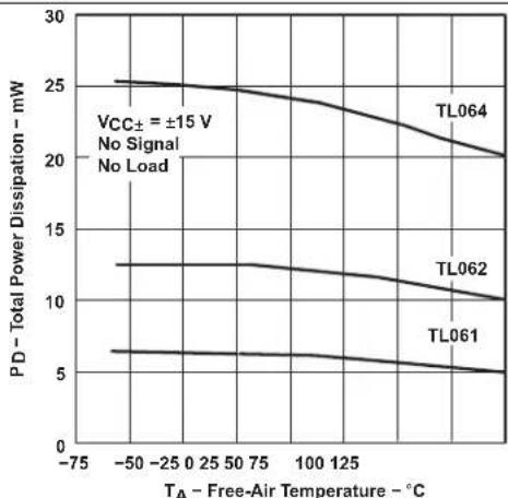
Figure 9. Total Power Dissipation vs Free-Air Temperature
line
| T_A - Free-Air Temperature - °C | CMRR - Common-Mode Rejection Ratio - dB | | ------------------------------- | --------------------------------------- | | -75 | 82.5 | | 0 | 86.0 | | 225 | 85.5 |Figure 10. All Except TL06_C Common-Mode Rejection Ratio vs Free-Air Temperature
line
| TA - Free-Air Temperature (°C) | Normalized Unity-Gain Bandwidth and Slew Rate | Normalized Phase Shift | | ------------------------------ | --------------------------------------------- | ---------------------- | | -75 | 1.15 | 1.02 | | 100759 | 1.00 | 1.01 | | 250-25 | 0.95 | 1.00 |Figure 11. Normalized Unity-Gain Bandwidth, Slew Rate, and Phase Shift vs Free-Air Temperature

line
| TA - Free-Air Temperature - °C | IIB - Input Bias Current - nA | | ------------------------------ | ----------------------------- | | -50 | 0.01 | | 0 | 0.04 | | 125 | 30.0 |Figure 12. Input Bias Current vs Free-Air Temperature
line
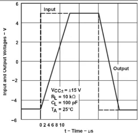
| t - Time (μs) | Input (V) | Output (V) | | ------------- | --------- | ---------- | | 0 | -5 | -5 | | 2 | -5 | -5 | | 4 | -2 | -2 | | 6 | 2 | 2 | | 8 | 5 | 5 | | 10 | 5 | 5 | | ∞ | -5 | -5 |Figure 13. Voltage-Follower Large-Signal Pulse Response vs Time

line
| t - Elapsed Time - µs | VO - Output Voltage - mV | | --------------------- | ------------------------ | | 0.0 | 0 | | 0.2 | 18 | | 0.4 | 21 | | 0.6 | 20 | | 0.8 | 20 | | 1.0 | 20 | | 1.2 | 20 | | 1.4 | 20 |Figure 14. Output Voltage vs Elapsed Time

line
| f - Frequency - Hz | Vn - Equivalent Input Noise Voltage - nV/√Hz | | ------------------ | ------------------------------------------- | | 10 | 90 | | 40 | 70 | | 100 | 60 | | 400 | 50 | | 1k | 45 | | 4k | 40 | | 10k | 40 | | 40k | 40 | | 100k | 40 |Figure 15. Equivalent Input Noise Voltage vs Frequency
7ParameterMeasurementInformation
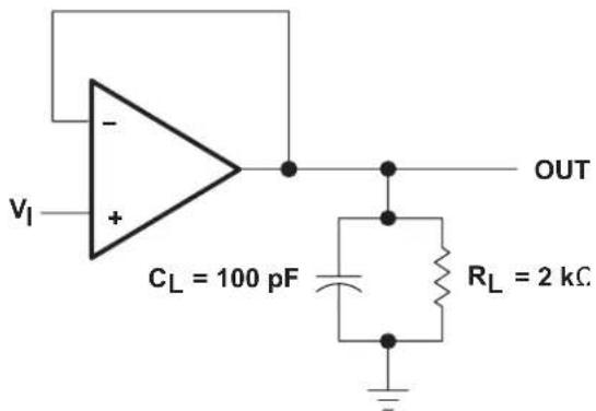
text_image
V_I + - CL = 100 pF R_L = 2 kΩ OUTFigure16. Unity-GainAmplifier
text_image
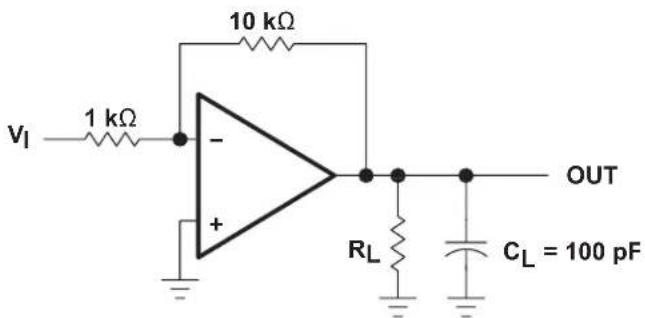
10 kΩ 1 kΩ V_I - + OUT R_L C_L = 100 pFFigure17.Gain-of-10InvertingAmplifier
text_image
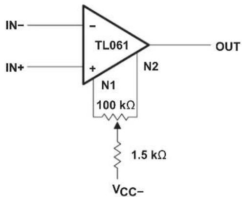
IN- + IN+ TL061 N2 OUT N1 100 kΩ 1.5 kΩ VCC-Figure18.InputOffset-VoltageNullCircuit
8DetailedDescription
8.1Overview
The JFET-inputoperationalamplifiers of the TL06x series are designed as low-power versions of the TL08x series amplifiers. They feature high input impedance, wide bandwidth, high slew rate, and low input offset and input bias currents. The TL06x series features the same terminal assignments as the TL07x and TL08x series. Each of these JFET-inputoperational amplifiers incorporates well-matched, high-voltage JFET and bipolar transistors in an integrated circuit.
TheC-suffixdevicesarecharacterizedforoperationfrom0°Cto70°C. TheI-suffixdevicesarecharacterizedfor operation from -40°C to 85°C, and the M-suffix devices are characterized for operation over the full military temperaturerangeof-55°Cto125°C.
8.2FunctionalBlockDiagram
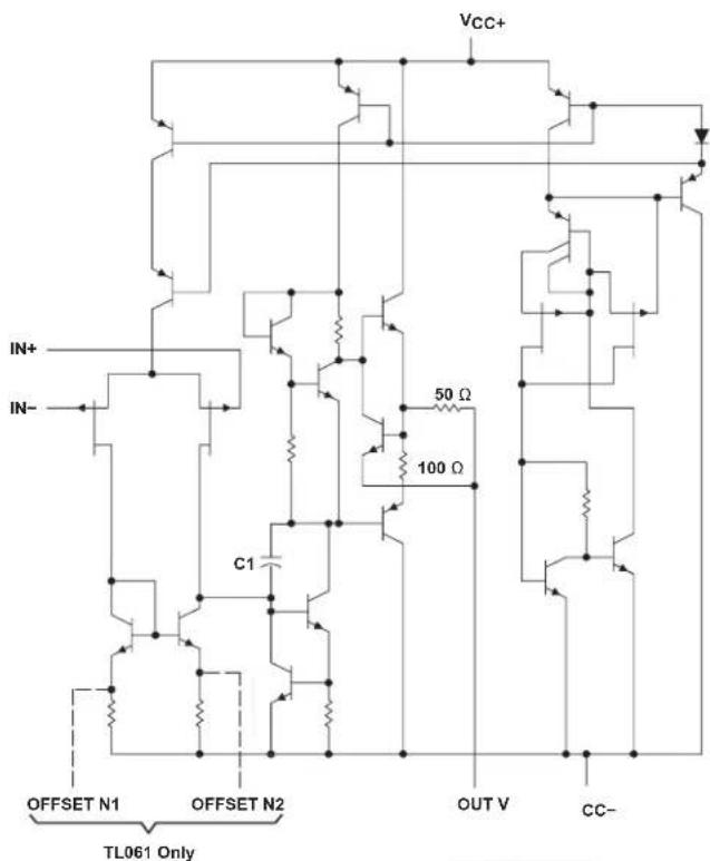
text_image
VCC+ IN+ IN- 50 Ω 100 Ω C1 OFFSET N1 OFFSET N2 OUT V CC- TL061 OnlyC1 = 10 pF on TL061, TL062, and TL064 Component values shown are nominal.
8.3FeatureDescription
8.3.1 Common-ModeRejectionRatio
The common-moderejection ratio (CMRR) of an amplifier is same as a measure of how well the device rejects unwanted inputs signals common to both input leads. It is found by taking the ratio of the change in input offset voltage to the change in the input voltage and converting to decibels. Ideally the CMRR is infinite, but in practice, amplifiers are designed to have it as high as possible. The CMRR of this device is 86dB.
8.3.2SlewRate
Theslewrateistherateatwhichanoperationalamplifiercchangeitsoutputwhenthereisachangeonthe input. Thesedeviceshavea3.5-V/μsslewrate.
8.4DeviceFunctionalModes
Thesedevicesarepoweredonwhenthesupplyisconnected. Thisdevicecanbeoperatedasasinglesupply operationalamplifierordualsupplyamplifierdependingontheapplication.
9ApplicationsandImplementation
NOTE
InformationinthefollowingapplicationssectionsisnotpartoftheTlcomponent specification,andTldoesnotwarrantitsaccuracyorcompleteness.TI'scustomersare responsiblefordeterminingsuitabilityofcomponentsfortheirpurposes.Customersshould validateandtesttheirdesignimplementationtoconfirmsystemfunctionality.
9.1 Application Information
The TL06xseries of operational amplifiers can be used in countless applications. The few applications in this section show principles used in all application so these parts.
9.2 Typical Applications
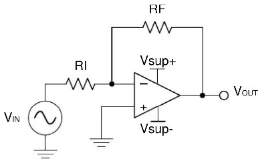
9.2.1 InvertingAmplifierApplication
Atypical application for an operational amplifier in an inverting amplifier. This amplifies a positive voltage on the input, and makes an negative voltage of the same magnitude. In the same manner, it also makes negative voltages positive.
text_image
V_IN RI RF Vsup+ - + Vsup- VOUTFigure19. Schematic for Inverting Amplifier Application
9.2.1.1 DesignRequirements
Thesupplyvoltagemustbechosensuchthatitislargerthantheinputvoltagerangeandoutputrange. For instance, this application will scale as signal of ±0.5Vto±1.8V . Setting the supply at ±12Vissufficientto accommodatethisapplication.
9.2.1.2 Detailed Design Procedure
Determinethegainrequiredbytheinvertingamplifier:
$$ A _ {v} = \frac {V O U T}{V I N} \tag {1} $$
$$ A _ {v} = \frac {1 . 8}{- 0 . 5} = - 3. 6 \tag {2} $$
Oncethedesiredgainisdetermined,chooseavalueforRIorRF.Choosingavalueinthekilohmrangeis desirablebecausetheamplifiercircuitwillusecurrentsinthemilliamprange.Thisensuresthepartwillnotdraw too much current. This example will choose 10 kΩ for RI which means 36 kΩ will be used for RF. This was determinedbyEquation3.
$$ A _ {v} = - \frac {R F}{R I} \tag {3} $$
Typical Applications (continued)
9.2.1.3 Application Curve
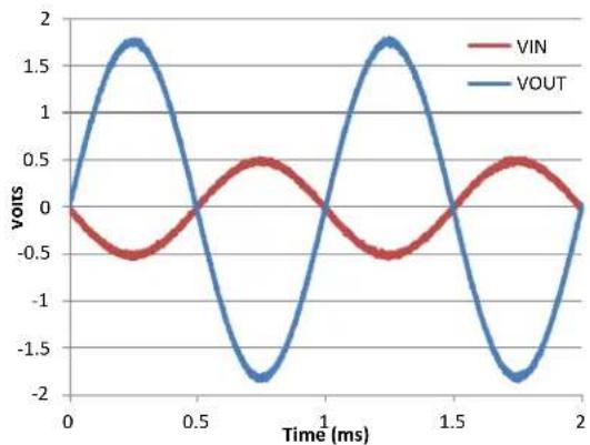
line
| Time (ms) | VIN | VOUT | | --------- | ---- | ---- | | 0.0 | 0.0 | 0.0 | | 0.5 | -0.5 | 1.8 | | 1.0 | 0.5 | -2.0 | | 1.5 | -0.5 | 1.8 | | 2.0 | 0.0 | 0.0 |Figure 20. Input and Output Voltages of the Inverting Amplifier
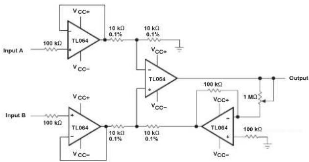
9.3 System Examples
9.3.1 General Applications
text_image
Input A 100 kΩ VCC+ TL054 10 kΩ 0.1% 10 kΩ 0.1% VCC+ TL064 + VCC- 100 kΩ Output VCC+ TL064 + VCC+ 1 MΩ VCC- 100 kΩ Input B 100 kΩ VCC+ TL064 + VCC-Figure 21. Instrumentation Amplifier
text_image
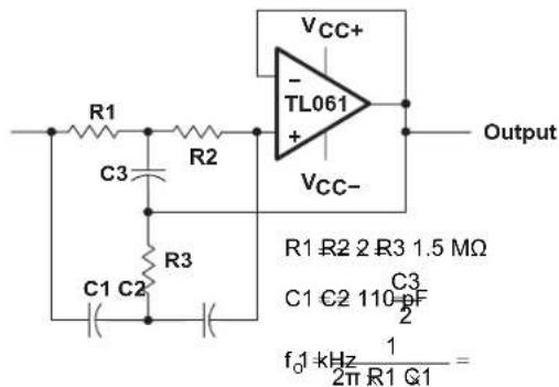
R1 C3 R2 C1 C2 R3 VCC+ - TL061 + VCC- Output R1 R2 2 R3 1.5 MΩ C1 C2 110 ΩF f0 1 kHz 1/2π R1 Q1 =Figure 23. High-Q Notch Filter
text_image
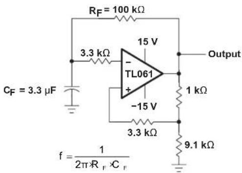
RF = 100 kΩ 3.3 kΩ TL061 -15 V Output CF = 3.3 μF -15 V 1 kΩ 3.3 kΩ 9.1 kΩ f = 1 / (2π*R_F × C_F)Figure 22. 0.5-Hz Square-Wave Oscillator
text_image
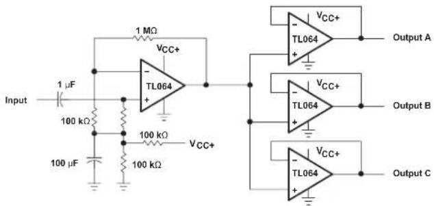
Input 1 μF 100 kΩ 100 μF 1 MΩ VCC+ TL064 + - VCC+ TL064 + - VCC+ TL064 + - Output A Output B Output CFigure 24. Audio-Distribution Amplifier
SystemExamples(continued)

text_image
TIL601 5 kΩ 10 kΩ 10 kΩ 10 kΩ 100 pF 10 kΩ 10 kΩ 10 kΩ 15 V + TL061 - Output -15 V
text_image
0.1 Fμ 10 kΩ 50 Ω 10 kΩ 0.1 μF 10 kΩ TL061 N1 250 kΩ N2 VCC+ 1 MΩ OutputFigure25.Low-LevelLightDetectorPreamplifierFigure26.ACAmplifier
text_image
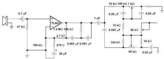
0.1 μF 47 kΩ TL061 1.2 MO 100 kΩ 2.7 kΩ 270 Ω + 20 μF 100 kΩ 10 kΩ 100 kΩ 1 kΩ 0.08 μF 0.06 μF 10 kΩ 0.002 μF 50 kΩ 100 kΩ 50 kΩ 10 kΩ 0.02 μF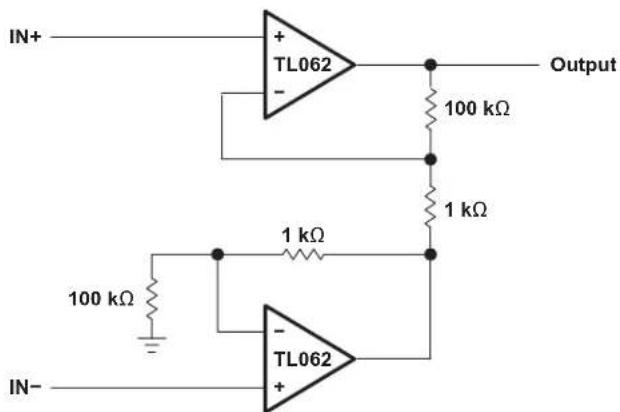
text_image
IN+ + TL062 - Output 100 kΩ 1 kΩ 1 kΩ 100 kΩ - TL062 + IN-Figure27. MicrophonePreamplifierWithToneFigure28. InstrumentationAmplifier Control
SystemExamples(continued)
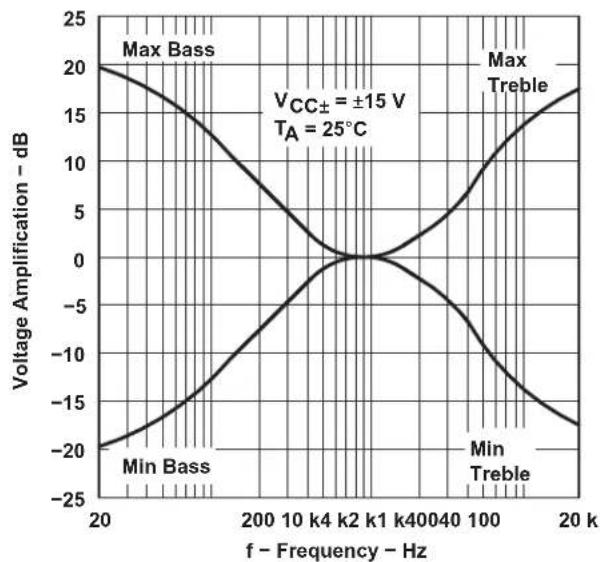
IC PREAMPLIFIER RESPONSE CHARACTERISTICS
line
| Frequency (Hz) | Max Bass (dB) | Max Treble (dB) | | -------------- | ------------- | --------------- | | 20 | 20 | -20 | | 200 | 10 | -10 | | 100 | 0 | 0 | | 20 | -20 | 20 |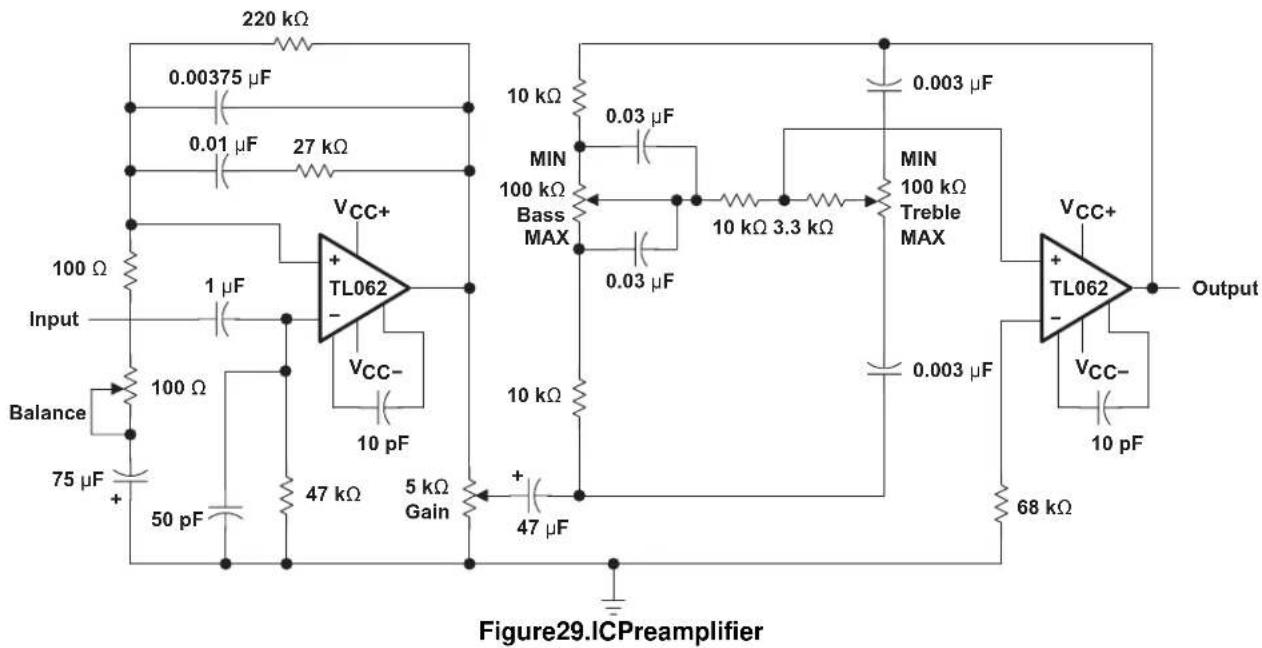
text_image
220 kΩ 0.00375 μF 0.01 μF 27 kΩ 100 Ω Input Balance 75 μF + 50 pF 1 μF 100 Ω VCC+ TL062 - VCC- 10 pF 47 kΩ 5 kΩ Gain 10 kΩ MIN 100 kΩ Bass MAX 0.03 μF 10 kΩ 3.3 kΩ 0.03 μF MIN 100 kΩ Treble MAX 0.003 μF 10 pF VCC+ TL062 - Output 68 kΩ Figure29.ICPreamplifier10PowerSupplyRecommendations
CAUTION
Supplyvoltageslargerthan36Vforasinglesupply,oroutsidetherangeof±18Vfor a dual supply can permanently damage the device (see the Absolute Maximum Ratings).
Place 0.1- F bypass capacitors close to the power-supply pins to reduce errors coupling in from noisy or high impedance power supplies. For more detailed information on bypass capacitor placement, refer to the Layout.
11Layout
11.1 LayoutGuidelines
Forbestoperationalperformanceofthedevice,usegoodPCBlayoutpractices,including:
- Noisecanpropagateintoanalogcircuitrythroughthepowerpinsofthecircuitasawhole,aswellasthe operationalamplifier.Bypasscapacitorsareusedtoreducethecouplednoisebyprovidinglowimpedance powersourceslocaltotheanalogcircuitry.
- Connect low-ESR, 0.1-μF ceramic bypass capacitors between each supply pin and ground, placed as closetothedeviceaspossible.AsinglebypasscapacitorfromV+togroundisapplicableforsingle supplyapplications.
- Separate grounding for analog and digital portions of circuitry is one of the simplest and most-effective methodsofnoisesuppression. OneormorelayeronmultilayerPCBsareusuallydevotedtogroundplanes. AgroundplanehelpsdistributeheatandreducesEMlnoisepickup.Makesuretophysicallyseparatedigital andanaloggrounds, payingattentiontotheflowofthegroundcurrent.Formoredetailedinformation,referto CircuitBoardLayoutTechniques,(SLOA089).
- Toreduceparasitic coupling, run the input traces as far away from the supply or output traces as possible. If it is not possible to keep them separate, it is much better to cross the sensitivetrace perpendicular as opposed to in parallel with the noisy trace.
- Placetheexternalcomponentsasclosetothedeviceaspossible.KeepingRFandRGclosetotheinverting inputminimizesparasiticcapacitance,asshowninLayoutExamples.
- Keepthelengthofinputtracesasshortaspossible.Alwaysrememberthattheinputtracesarethemost sensitivepartofthecircuit.
- Consideradriven, low-impedance guardring around the critical traces. Aguardring cans significantly reduce leakage currents from nearby trace that are at different potentials.
11.2 LayoutExamples
text_image
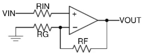
VIN RIN + - RG RF VOUTFigure30. OperationalAmplifierSchematicforNoninvertingConfiguration
flowchart
graph TD
    A["Run the input traces as far away from the supply lines as possible"] --> B["Place components close to device and to each other to reduce parasitic errors"]
    B --> C["RF"]
    C --> D["RC"]
    D --> E["NC"]
    D --> F["IN1-"]
    D --> G["IN1+"]
    D --> H["VCC-"]
    E --> I["Output"]
    F --> I
    G --> I
    H --> I
    I --> J["Use low-ESR, ceramic bypass capacitor"]
    K["Only needed for dual-supply operation"] --> L["Ground (GND) plane on another layerVOUT"]
    M["GND"] --> N["Ground (GND)"]
    O["GND"] --> P["Ground (GND)"]
    Q["VS+"] --> R["Output"]
Figure31. OperationalAmplifierBoardLayoutforNoninvertingConfiguration
12DeviceandDocumentationSupport
12.1 DocumentationSupport
12.1.1 Related Documentation
Forrelateddocumentation,seethefollowing: CircuitBoardLayoutTechniques,SLOA089
12.2RelatedLinks
Thetablebelowlistsquickaccesslinks.Categoriesincludetechnicaldocuments,supportandcommunity resources,toolsandsoftware,andquickaccesstosampleorbuy.
Table2.RelatedLinks
| PARTSPRODUCTFOLDERSAMPLE&BUY | TECHNICALTOOLS&SUPPORT&DOCUMENTSSOFTWARE COMMUNITY | ||||
| TL061 | Click here | Click here | Click here | Click here | Click here |
| TL061A | Click here | Click here | Click here | Click here | Click here |
| TL061B | Click here | Click here | Click here | Click here | Click here |
| TL062 | Click here | Click here | Click here | Click here | Click here |
| TL062A | Click here | Click here | Click here | Click here | Click here |
| TL062B | Click here | Click here | Click here | Click here | Click here |
| TL064 | Click here | Click here | Click here | Click here | Click here |
| TL064A | Click here | Click here | Click here | Click here | Click here |
| TL064B | Click here | Click here | Click here | Click here | Click here |
12.3 Community Resources
The following links connect to TI community resources. Linked contents are provided "AS IS" by the respective contributors. They do not constitute TI specifications and do not necessarily reflect TI's views; see TI's Terms of Use.
TI E2E™ Online Community TI's Engineer-to-Engineer (E2E) Community. Created to foster collaboration amongengineers.Ate2e.ti.com,youcanaskquestions,shareknowledge,exploreideasandhelp solveproblemswithfellowengineers.
Design Support TI's Design Support Quickly find helpful E2E forums along with design support tools and contactinformationfortechnicalsupport.
12.4Trademarks
E2EisatrademarkofTexasInstruments.
12.5ElectrostaticDischargeCaution

These devices have limited built-in ESD protection. The leads should be shorted together or the device placed in conductive foam duringstorageorhandlingtopreventelectrostaticdamagetotheMOSgates.
12.6Glossary
SLYZ022 — TIGlossary.
This glossarylistsandexplainsterms,acronyms,anddefinitions.
13Mechanical, Packaging, and Orderable Information
The following pages include mechanical packaging and orderable information. This information is the most current data available for the designated devices. This data is subject to change without notice and revision of thisdocument.Forbrowserbasedversionsofthisdatasheet,refertothelefthandnavigation.
PACKAGING INFORMATION
| Orderable Device Status(1) | Package Type | Package Drawing | Pins | Package Qty | Eco Plan(2) | Lead finish/ Ball material(6) | MSL Peak Temp(3) | Op Temp (°C) | Device Marking(4/5) | Samples | |
| 81023022A ACTIVE LCCC FK 20 1 Non-RoHS | & Green | SNPB N / A for Pkg Type -55 to 125 81023022A | TL062MFKB | Samples | |||||||
| 8102302PA ACTIVE CDIP JG 8 1 Non-RoHS | & Green | SNPB N / A for Pkg Type -55 to 125 8102302PA | TL062M | Samples | |||||||
| 81023032A ACTIVE LCCC FK 20 1 Non-RoHS | & Green | SNPB N / A for Pkg Type -55 to 125 81023032A | TL064MFKB | Samples | |||||||
| 8102303CA ACTIVE CDIP J 14 1 Non-RoHS | & Green | SNPB N / A for Pkg Type -55 to 125 8102303CA | TL064MJB | Samples | |||||||
| 8102303DA ACTIVE | CFP W | 14 1 Non-RoHS | & Green | SNPB N / A for Pkg Type -55 to 125 8102303DA | TL064MWB | Samples | |||||
| TL061ACD | ACTIVE | SOIC | D | 8 | 75 | RoHS & Green | NIPDAU | Level-1-260C-UNLIM | 0 to 70 | 061AC | Samples |
| TL061ACDE4 | ACTIVE | SOIC | D | 8 | 75 | RoHS & Green | NIPDAU | Level-1-260C-UNLIM | 0 to 70 | 061AC | Samples |
| TL061ACDR | ACTIVE | SOIC | D | 8 | 2500 | RoHS & Green | NIPDAU | Level-1-260C-UNLIM | 0 to 70 | 061AC | Samples |
| TL061ACP | ACTIVE | PDIP | P | 8 | 50 | RoHS & Green | NIPDAU | N / A for Pkg Type | 0 to 70 | TL061ACP | Samples |
| TL061BCP | ACTIVE | PDIP | P | 8 | 50 | RoHS & Green | NIPDAU | N / A for Pkg Type | 0 to 70 | TL061BCP | Samples |
| TL061BCPE4 | ACTIVE | PDIP | P | 8 | 50 | RoHS & Green | NIPDAU | N / A for Pkg Type | 0 to 70 | TL061BCP | Samples |
| TL061CD | ACTIVE | SOIC | D | 8 | 75 | RoHS & Green | NIPDAU | Level-1-260C-UNLIM | 0 to 70 | TL061C | Samples |
| TL061CDR | ACTIVE | SOIC | D | 8 | 2500 | RoHS & Green | NIPDAU | Level-1-260C-UNLIM | 0 to 70 | TL061C | Samples |
| TL061CP | ACTIVE | PDIP | P | 8 | 50 | RoHS & Green | NIPDAU | N / A for Pkg Type | 0 to 70 | TL061CP | Samples |
| TL061CPSR | ACTIVE | SO | PS | 8 | 2000 | RoHS & Green | NIPDAU | Level-1-260C-UNLIM | 0 to 70 | T061 | Samples |
| TL061ID | ACTIVE | SOIC | D | 8 | 75 | RoHS & Green | NIPDAU | Level-1-260C-UNLIM | -40 to 85 | TL061I | Samples |
| TL061IDR | ACTIVE | SOIC | D | 8 | 2500 | RoHS & Green | NIPDAU | Level-1-260C-UNLIM | -40 to 85 | TL061I | Samples |
| TL061IDRG4 | ACTIVE | SOIC | D | 8 | 2500 | RoHS & Green | NIPDAU | Level-1-260C-UNLIM | -40 to 85 | TL061I | Samples |
| TL061IP | ACTIVE | PDIP | P | 8 | 50 | RoHS & Green | NIPDAU | N / A for Pkg Type | -40 to 85 | TL061IP | Samples |
Addendum-Page 1
| Orderable Device Status(1) | Package Type | Package Drawing | Pins | Package Qty | Eco Plan(2) | Lead finish/ Ball material(6) | MSL Peak Temp(3) | Op Temp (°C) | Device Marking(4-5) | Samples | |
| TL061IPE4 ACTIVE PDIP P 8 50 RoHS & Green NIPDAU N / A for Pkg Type -40 to 85 TL061IP | Samples | ||||||||||
| TL062ACD ACTIVE SOIC D 8 75 RoHS & Green NIPDAU Level-1-260C-UNLIM 0 to 70 062AC | Samples | ||||||||||
| TL062ACDE4 | ACTIVE | SOIC | D | 8 | 75 | RoHS & Green | NIPDAU | Level-1-260C-UNLIM | 0 to 70 | 062AC | Samples |
| TL062ACDR | ACTIVE | SOIC | D | 8 | 2500 | RoHS & Green | NIPDAU | Level-1-260C-UNLIM | 0 to 70 | 062AC | Samples |
| TL062ACDRE4 | ACTIVE | SOIC | D | 8 | 2500 | RoHS & Green | NIPDAU | Level-1-260C-UNLIM | 0 to 70 | 062AC | Samples |
| TL062ACDRG4 | ACTIVE | SOIC | D | 8 | 2500 | RoHS & Green | NIPDAU | Level-1-260C-UNLIM | 0 to 70 | 062AC | Samples |
| TL062ACP | ACTIVE | PDIP | P | 8 | 50 | RoHS & Green | NIPDAU | N / A for Pkg Type | 0 to 70 | TL062ACP | Samples |
| TL062ACPSR | ACTIVE | SO | PS | 8 | 2000 | RoHS & Green | NIPDAU | Level-1-260C-UNLIM | 0 to 70 | T062A | Samples |
| TL062ACPSRG4 | ACTIVE | SO | PS | 8 | 2000 | RoHS & Green | NIPDAU | Level-1-260C-UNLIM | 0 to 70 | T062A | Samples |
| TL062BCD | ACTIVE | SOIC | D | 8 | 75 | RoHS & Green | NIPDAU | Level-1-260C-UNLIM | 0 to 70 | 062BC | Samples |
| TL062BCDG4 | ACTIVE | SOIC | D | 8 | 75 | RoHS & Green | NIPDAU | Level-1-260C-UNLIM | 0 to 70 | 062BC | Samples |
| TL062BCDR | ACTIVE | SOIC | D | 8 | 2500 | RoHS & Green | NIPDAU | Level-1-260C-UNLIM | 0 to 70 | 062BC | Samples |
| TL062BCP | ACTIVE | PDIP | P | 8 | 50 | RoHS & Green | NIPDAU | N / A for Pkg Type | 0 to 70 | TL062BCP | Samples |
| TL062BCPE4 | ACTIVE | PDIP | P | 8 | 50 | RoHS & Green | NIPDAU | N / A for Pkg Type | 0 to 70 | TL062BCP | Samples |
| TL062CD | ACTIVE | SOIC | D | 8 | 75 | RoHS & Green | NIPDAU | Level-1-260C-UNLIM | 0 to 70 | TL062C | Samples |
| TL062CDE4 | ACTIVE | SOIC | D | 8 | 75 | RoHS & Green | NIPDAU | Level-1-260C-UNLIM | 0 to 70 | TL062C | Samples |
| TL062CDR | ACTIVE | SOIC | D | 8 | 2500 | RoHS & Green | NIPDAU | Level-1-260C-UNLIM | 0 to 70 | TL062C | Samples |
| TL062CDRE4 | ACTIVE | SOIC | D | 8 | 2500 | RoHS & Green | NIPDAU | Level-1-260C-UNLIM | 0 to 70 | TL062C | Samples |
| TL062CDRG4 | ACTIVE | SOIC | D | 8 | 2500 | RoHS & Green | NIPDAU | Level-1-260C-UNLIM | 0 to 70 | TL062C | Samples |
| TL062CP | ACTIVE | PDIP | P | 8 | 50 | RoHS & Green | NIPDAU | N / A for Pkg Type | 0 to 70 | TL062CP | Samples |
| TL062CPE4 | ACTIVE | PDIP | P | 8 | 50 | RoHS & Green | NIPDAU | N / A for Pkg Type | 0 to 70 | TL062CP | Samples |
| TL062CPS ACTIVE SO PS 8 80 RoHS & Green NIPDAU Level-1-260C-UNLIM 0 to 70 T062 | Samples | ||||||||||
| TL062CPSR ACTIVE SO PS 8 2000 RoHS & Green NIPDAU Level-1-260C-UNLIM 0 to 70 T062 | Samples | ||||||||||
| TL062CPW | ACTIVE | TSSOP | PW | 8 | 150 | RoHS & Green | NIPDAU | Level-1-260C-UNLIM | 0 to 70 | T062 | Samples |
| TL062CPWG4 | ACTIVE | TSSOP | PW | 8 | 150 | RoHS & Green | NIPDAU | Level-1-260C-UNLIM | 0 to 70 | T062 | Samples |
| TL062CPWR | ACTIVE | TSSOP | PW | 8 | 2000 | RoHS & Green | NIPDAU | Level-1-260C-UNLIM | 0 to 70 | T062 | Samples |
| TL062CPWRG4 | ACTIVE | TSSOP | PW | 8 | 2000 | RoHS & Green | NIPDAU | Level-1-260C-UNLIM | 0 to 70 | T062 | Samples |
| TL062ID | ACTIVE | SOIC | D | 8 | 75 | RoHS & Green | NIPDAU | Level-1-260C-UNLIM | -40 to 85 | TL062I | Samples |
| TL062IDG4 | ACTIVE | SOIC | D | 8 | 75 | RoHS & Green | NIPDAU | Level-1-260C-UNLIM | -40 to 85 | TL062I | Samples |
| TL062IDR | ACTIVE | SOIC | D | 8 | 2500 | RoHS & Green | NIPDAU | Level-1-260C-UNLIM | -40 to 85 | TL062I | Samples |
| TL062IDRG4 | ACTIVE | SOIC | D | 8 | 2500 | RoHS & Green | NIPDAU | Level-1-260C-UNLIM | -40 to 85 | TL062I | Samples |
| TL062IP | ACTIVE | PDIP | P | 8 | 50 | RoHS & Green | NIPDAU | N / A for Pkg Type | -40 to 85 | TL062IP | Samples |
| TL062IPE4 | ACTIVE | PDIP | P | 8 | 50 | RoHS & Green | NIPDAU | N / A for Pkg Type | -40 to 85 | TL062IP | Samples |
| TL062IPWR | ACTIVE | TSSOP | PW | 8 | 2000 | RoHS & Green | NIPDAU | Level-1-260C- UNLIM | -40 to 85 | Z062 | Samples |
| TL062IPWRG4 | ACTIVE | TSSOP | PW | 8 | 2000 | RoHS & Green | NIPDAU | Level-1-260C-UNLIM | -40 to 85 | Z062 | Samples |
| TL062MFKB ACTIVE LCCC | FK 20 1 | Non-RoHS | & Green | SNPB N / A for Pkg Type | -55 to 125 | 81023022ATL062MFKB | Samples | ||||
| TL062MJG | ACTIVE | CDIP | JG | 8 | 1 | Non-RoHS & Green | SNPB N / A for Pkg Type | -55 to 125 | TL062MJG | Samples | |
| TL062MJGB | ACTIVE | CDIP | JG | 8 | 1 | Non-RoHS & Green | SNPB N / A for Pkg Type | -55 to 125 | 8102302PATL062M | Samples | |
| TL064ACD | ACTIVE | SOIC | D | 14 | 50 | RoHS & Green | NIPDAU | Level-1-260C-UNLIM | 0 to 70 | TL064AC | Samples |
| TL064ACDR | ACTIVE | SOIC | D | 14 | 2500 | RoHS & Green | NIPDAU | Level-1-260C-UNLIM | 0 to 70 | TL064AC | Samples |
| TL064ACDRE4 | ACTIVE | SOIC | D | 14 | 2500 | RoHS & Green | NIPDAU | Level-1-260C-UNLIM | 0 to 70 | TL064AC | Samples |
| Orderable Device Status(1) | Package Type Package Drawing | Pins Package Qty | Eco Plan(2) | Lead finish/ Ball material(6) | MSL Peak Temp(3) | Op Temp (°C) | Device Marking(4-5) | Samples | |||
| TL064ACN ACTIVE PDIP N 14 25 RoHS & Green NIPDAU N / A for Pkg Type 0 to 70 TL064ACN | Samples | ||||||||||
| TL064BCD ACTIVE SOIC D 14 50 RoHS & Green NIPDAU Level-1-260C-UNLIM 0 to 70 TL064BC | Samples | ||||||||||
| TL064BCDG4 | ACTIVE SOIC D 14 50 RoHS & Green NIPDAU Level-1-260C-UNLIM 0 to 70 TL064BC | Samples | |||||||||
| TL064BCDR | ACTIVE | SOIC | D | 14 | 2500 | RoHS & Green | NIPDAU | Level-1-260C-UNLIM | 0 to 70 | TL064BC | |
| TL064BCN ACTIVE PDIP N 14 25 RoHS & Green NIPDAU N / A for Pkg Type 0 to 70 TL064BCN | Samples | ||||||||||
| TL064BCNE4 | ACTIVE PDIP N 14 25 RoHS & Green NIPDAU N / A for Pkg Type 0 to 70 TL064BCN | Samples | |||||||||
| TL064CD | ACTIVE SOIC D 14 50 RoHS & Green NIPDAU Level-1-260C-UNLIM 0 to 70 TL064C | Samples | |||||||||
| TL064CDE4 | ACTIVE SOIC D 14 50 RoHS & Green NIPDAU Level-1-260C-UNLIM 0 to 70 TL064C | Samples | |||||||||
| TL064CDR | ACTIVE | SOIC | D | 14 | 2500 | RoHS & Green | NIPDAU | Level-1-260C-UNLIM | 0 to 70 | TL064C | |
| TL064CDRE4 | ACTIVE | SOIC | D | 14 | 2500 | RoHS & Green | NIPDAU | Level-1-260C-UNLIM | 0 to 70 | TL064C | |
| TL064CN | ACTIVE PDIP N 14 25 RoHS & Green NIPDAU N / A for Pkg Type 0 to 70 TL064CN | Samples | |||||||||
| TL064CNSR | ACTIVE | SO | NS | 14 | 2000 | RoHS & Green | NIPDAU | Level-1-260C-UNLIM | 0 to 70 | TL064 | |
| TL064CPW | ACTIVE | TSSOP | PW | 14 | 90 | RoHS & Green | NIPDAU | Level-1-260C-UNLIM | 0 to 70 | T064 | |
| TL064CPWE4 | ACTIVE | TSSOP | PW | 14 | 90 | RoHS & Green | NIPDAU | Level-1-260C-UNLIM | 0 to 70 | T064 | |
| TL064CPWG4 | ACTIVE | TSSOP | PW | 14 | 90 | RoHS & Green | NIPDAU | Level-1-260C-UNLIM | 0 to 70 | T064 | |
| TL064CPWR | ACTIVE | TSSOP | PW | 14 | 2000 | RoHS & Green | NIPDAU | Level-1-260C-UNLIM | 0 to 70 | T064 | |
| TL064ID | ACTIVE | SOIC | D | 14 | 50 | RoHS & Green | NIPDAU | Level-1-260C-UNLIM | -40 to 85 | TL064I | |
| TL064IDG4 | ACTIVE | SOIC | D | 14 | 50 | RoHS & Green | NIPDAU | Level-1-260C-UNLIM | -40 to 85 | TL064I | |
| TL064IDR | ACTIVE | SOIC | D | 14 | 2500 | RoHS & Green | NIPDAU | SN | Level-1-260C-UNLIM | -40 to 85 | TL064I | |
| TL064IDRG4 | ACTIVE | SOIC | D | 14 | 2500 | RoHS & Green | NIPDAU | Level-1-260C-UNLIM | -40 to 85 | TL064I | |
| TL064IN | ACTIVE | PDIP | N | 14 | 25 | RoHS & Green | NIPDAU | N / A for Pkg Type | -40 to 85 | TL064IN | |
| Orderable Device Status(1) | Package Type | Package Drawing | Pins | Package Qty | Eco Plan(2) | Lead finish/ Ball material(6) | MSL Peak Temp(3) | Op Temp (°C) | Device Marking(4-5) | Samples | |
| TL064INE4 ACTIVE PDIP N 14 25 RoHS & Green NIPDAU N / A for Pkg Type -40 to 85 TL064IN | Samples | ||||||||||
| TL064INS | ACTIVE | SO | NS | 14 | 50 | RoHS & Green | NIPDAU | Level-1-260C-UNLIM | -40 to 85 | TL064I | Samples |
| TL064INSR | ACTIVE | SO | NS | 14 | 2000 | RoHS & Green | NIPDAU | Level-1-260C-UNLIM | -40 to 85 | TL064I | Samples |
| TL064IPWR | ACTIVE | TSSOP | PW | 14 | 2000 | RoHS & Green | NIPDAU | Level-1-260C-UNLIM | -40 to 85 | Z064 | Samples |
| TL064MFKB ACTIVE LCCC | FK 20 1 | Non-RoHS | & Green | SNPB N / A for Pkg Type | -55 to 125 | 81023032ATL064MFKB | Samples | ||||
| TL064MJ | ACTIVE CDIP J | 14 1 | Non-RoHS | & Green | SNPB N / A for Pkg Type | -55 to 125 | TL064MJ | Samples | |||
| TL064MJB | ACTIVE CDIP J | 14 1 | Non-RoHS | & Green | SNPB N / A for Pkg Type | -55 to 125 | 8102303CATL064MJB | Samples | |||
| TL064MWB | ACTIVE | CFP | W | 14 | 1 | Non-RoHS & Green | SNPB N / A for Pkg Type | -55 to 125 | 8102303DATL064MWB | Samples | |
(1) The marketing status values are defined as follows:
ACTIVE: Product device recommended for new designs.
LIFEBUY: TI has announced that the device will be discontinued, and a lifetime-buy period is in effect.
NRND: Not recommended for new designs. Device is in production to support existing customers, but TI does not recommend using this part in a new design.
PREVIEW: Device has been announced but is not in production. Samples may or may not be available.
OBSOLETE: TI has discontinued the production of the device.
(2) RoHS: TI defines "RoHS" to mean semiconductor products that are compliant with the current EU RoHS requirements for all 10 RoHS substances, including the requirement that RoHS substance do not exceed 0.1% by weight in homogeneous materials. Where designed to be soldered at high temperatures, "RoHS" products are suitable for use in specified lead-free processes. TI may reference these types of products as "Pb-Free".
RoHS Exempt: TI defines "RoHS Exempt" to mean products that contain lead but are compliant with EU RoHS pursuant to a specific EU RoHS exemption.
Green: TI defines "Green" to mean the content of Chlorine (Cl) and Bromine (Br) based flame retardants meet JS709B low halogen requirements of <=1000ppm threshold. Antimony trioxide based flame retardants must also meet the <=1000ppm threshold requirement.
(3) MSL, Peak Temp. - The Moisture Sensitivity Level rating according to the JEDEC industry standard classifications, and peak solder temperature.
(4) There may be additional marking, which relates to the logo, the lot trace code information, or the environmental category on the device.
(5) Multiple Device Markings will be inside parentheses. Only one Device Marking contained in parentheses and separated by a "\~" will appear on a device. If a line is indented then it is a continuation of the previous line and the two combined represent the entire Device Marking for that device.
(6) Lead finish/Ball material - Orderable Devices may have multiple material finish options. Finish options are separated by a vertical ruled line. Lead finish/Ball material values may wrap to two lines if the finish value exceeds the maximum column width.
Important Information and Disclaimer: The information provided on this page represents TI's knowledge and belief as of the date that it is provided. TI bases its knowledge and belief on information provided by third parties, and makes no representation or warranty as to the accuracy of such information. Efforts are underway to better integrate information from third parties. TI has taken and continues to take reasonable steps to provide representative and accurate information but may not have conducted destructive testing or chemical analysis on incoming materials and chemicals. TI and TI suppliers consider certain information to be proprietary, and thus CAS numbers and other limited information may not be available for release.
In no event shall TI's liability arising out of such information exceed the total purchase price of the TI part(s) at issue in this document sold by TI to Customer on an annual basis.
OTHER QUALIFIED VERSIONS OF TL062, TL062M, TL064, TL064M :
NOTE: Qualified Version Definitions:
• Catalog - TI's standard catalog product
• Military - QML certified for Military and Defense Applications
TAPE AND REEL INFORMATION

*All dimensions are nominal
| Device Package | Type | Package Drawing | Pins | SPQ Reel | Diameter (mm) | Reel Width W1 (mm) | A0 (mm) | B0 (mm) | K0 (mm) | P1 (mm) | W (mm) | Pin1 Quadrant |
| TL061ACDR SOIC D | 8 2500 3 | 30.0 12.4 | 6.4 5.2 | 2.1 8.0 12 | 0 Q1 | |||||||
| TL061CDR SOIC D | 8 2500 3 | 30.0 12.4 6 | 4.5.2 | 2.1 8.0 12 | 0 Q1 | |||||||
| TL061CDR SOIC D | 8 2500 3 | 30.0 12.4 6 | 4.5.2 | 2.1 8.0 12 | 0 Q1 | |||||||
| TL061CPSR SO PS | 8 2000 3 | 30.0 12.4 | 6.4 8. | 35 6.6 2.4 | 12.0 16.0 | Q1 | ||||||
| TL061IDR SOIC D | 8 2500 3 | 30.0 12.4 | 6.4 | 5.2 2.1 8. | 0 12.0 | Q1 | ||||||
| TL061IDR SOIC D | 8 2500 3 | 30.0 12.4 | 6.4 | 5.2 2.1 8. | 0 12.0 | Q1 | ||||||
| TL062ACDR SOIC D | 8 2500 3 | 30.0 12.4 | 6.4 5.2 | 2.1 8.0 12 | 0 Q1 | |||||||
| TL062ACPSR | SO PS | 8 20 | 00 33 | 0.0 16.4 8 | 35 6.6 2.4 | 12.0 16.0 | Q1 | |||||
| TL062BCDR SOIC D | 8 2500 3 | 30.0 12.4 | 6.4 5.2 | 2.1 8.0 12 | 0 Q1 | |||||||
| TL062CDR SOIC D | 8 2500 3 | 30.0 12.4 6 | 4.5.2 | 2.1 8.0 12 | 0 Q1 | |||||||
| TL062CDR SOIC D | 8 2500 3 | 30.0 12.4 6 | 4.5.2 | 2.1 8.0 12 | 0 Q1 | |||||||
| TL062CPSR SO PS | 8 2000 3 | 30.0 12.4 | 6.4 8. | 35 6.6 2.4 | 12.0 16.0 | Q1 | ||||||
| TL062CPWR | TSSOP PW | 8 | 2000 | 30.0 12.4 | 7.0 3.6 1.6 | 8.0 12.0 | Q1 | |||||
| TL062CPWRG4 TSS OP PW | 8 2000 | 30.0 | 12.4 7.0 3.6 | 1.6 8.0 | 12.0 | Q1 | ||||||
| TL062IDR SOIC D | 8 2500 3 | 30.0 12.4 | 6.4 | 5.2 2.1 8. | 0 12.0 | Q1 | ||||||
| TL062IDR SOIC D | 8 2500 3 | 30.0 12.4 | 6.4 | 5.2 2.1 8. | 0 12.0 | Q1 | ||||||
| TL062IPWR | TSSOP PW | 8 | 2000 | 30.0 12.4 | 7.0 3.6 1.6 | 8.0 12.0 | Q1 | |||||
| TL064ACDR SOIC D | 14 | 2500 | 30.0 | 6.4 6.5 9. | 0 2.1 8. | 16.0 | Q1 | |||||
| TL064BCDR SOIC D | 14 2500 | 330.0 16.4 | 6.5 9 | 0 2.1 8.0 1 | 6.0 Q1 | |||||||
| TL064CDR SOIC D | 14 2500 | 330.0 16.4 | 6.5 9.0 | 2.1 8.0 1 | 6.0 Q1 | |||||||
| TL064CNSR SO NS | 14 2000 | 330.0 16.4 | 8.2 10 | .5 2.5 12.0 | 16.0 Q1 | |||||||
| TL064CPWR | TSSOP PW 14 | 2000 | 330.0 12.4 | 6.9 5.6 1 | 6 8.0 12.0 | Q1 | ||||||
| TL064IDR | SOIC D | 14 2500 3 | 30.0 1 | 6.4 6.5 9.0 | 2.1 8.0 1 | 6.0 Q1 | ||||||
| TL064IDRG4 | SOIC D | 14 2500 3 | 30.0 1 | 6.4 6.5 9.0 | 2.1 8.0 1 | 6.0 Q1 | ||||||
| TL064INSR | SO | NS | 14 | 2000 | 330.0 | 16.4 | 8.2 | 10.5 | 2.5 | 12.0 | 16.0 | Q1 |
| TL064IPWR | TSSOP PW 14 | 2000 | 330.0 12.4 | 6.9 5.6 1 | 6 8.0 12.0 | Q1 | ||||||

text_image
TAPE AND REEL BOX DIMENSIONS W L*All dimensions are nominal
| Device | Package Type | Package Drawing | Pins | SPQ | Length (mm) | Width (mm) | Height (mm) |
| TL061ACDR | SOIC | D | 8 | 2500 | 340.5 | 336.1 | 25.0 |
| TL061CDR | SOIC | D | 8 | 2500 | 853.0 | 449.0 | 35.0 |
| TL061CDR | SOIC | D | 8 | 2500 | 340.5 | 336.1 | 25.0 |
| TL061CPSR | SO | PS | 8 | 2000 | 853.0 | 449.0 | 35.0 |
| TL061IDR | SOIC | D | 8 | 2500 | 340.5 | 336.1 | 25.0 |
| TL061IDR | SOIC | D | 8 | 2500 | 853.0 | 449.0 | 35.0 |
| TL062ACDR | SOIC | D | 8 | 2500 | 340.5 | 336.1 | 25.0 |
| TL062ACPSR | SO | PS | 8 | 2000 | 853.0 | 449.0 | 35.0 |
| TL062BCDR | SOIC | D | 8 | 2500 | 340.5 | 336.1 | 25.0 |
| TL062CDR SOIC D | 8 2500 340.5 336.1 | 25.0 | |||||
| TL062CDR SOIC D | 8 2500 853.0 449.0 | 35.0 | |||||
| TL062CPSR SO PS | 8 2000 853.0 449.0 | 35.0 | |||||
| TL062CPWR | TSSOP | PW | 8 | 2000 | 853.0 | 449.0 | 35.0 |
| TL062CPWRG4 | TSSOP | PW | 8 | 2000 | 853.0 | 449.0 | 35.0 |
| TL062IDR SOIC D | 8 2500 853.0 449.0 | 35.0 | |||||
| TL062IDR SOIC D | 8 2500 340.5 336.1 | 25.0 | |||||
| TL062IPWR | TSSOP | PW | 8 | 2000 | 853.0 | 449.0 | 35.0 |
| TL064ACDR | SOIC D 14 | 2500 853.0 449.0 | 35.0 | ||||
| TL064BCDR | SOIC D 14 | 2500 853.0 449.0 | 35.0 | ||||
| TL064CDR SOIC D | 14 2500 853.0 | 449.0 35.0 | |||||
| TL064CNSR | SO | NS | 14 | 2000 | 367.0 | 367.0 | 38.0 |
| TL064CPWR | TSSOP | PW | 14 | 2000 | 853.0 | 449.0 | 35.0 |
| TL064IDR SOIC D | 14 | 2500 853.0 449.0 | 35.0 | ||||
| TL064IDRG4 | SOIC D 14 | 2500 853.0 449.0 | 35.0 | ||||
| TL064INSR SO NS | 14 | 2000 853.0 449.0 | 35.0 | ||||
| TL064IPWR | TSSOP | PW | 14 | 2000 | 853.0 | 449.0 | 35.0 |
TUBE
text_image
T - Tube height L - Tube length W - Tube width B - Alignment groove width*All dimensions are nominal
| Device | Package Name | Package Type | Pins | SPQ | L (mm) | W (mm) | T (μm) | B (mm) |
| 81023022A FK LCQ | C 20 1 506.98 12.06 | 2030 NA | ||||||
| 81023032A FK LCQ | C 20 1 506.98 12.06 | 2030 NA | ||||||
| TL061ACD | D | SOIC | 8 | 75 | 507 | 8 | 3940 | 4.32 |
| TL061ACDE4 | D | SOIC | 8 | 75 | 507 | 8 | 3940 | 4.32 |
| TL061ACP | P | PDIP | 8 | 50 | 506 | 13.97 | 11230 | 4.32 |
| TL061BCP | P | PDIP | 8 | 50 | 506 | 13.97 | 11230 | 4.32 |
| TL061BCPE4 | P | PDIP | 8 | 50 | 506 | 13.97 | 11230 | 4.32 |
| TL061CD | D | SOIC | 8 | 75 | 507 | 8 | 3940 | 4.32 |
| TL061CD | D | SOIC | 8 | 75 | 506.6 | 8 | 3940 | 4.32 |
| TL061CP | P | PDIP | 8 | 50 | 506 | 13.97 | 11230 | 4.32 |
| TL061ID | D | SOIC | 8 | 75 | 506.6 | 8 | 3940 | 4.32 |
| TL061ID | D | SOIC | 8 | 75 | 507 | 8 | 3940 | 4.32 |
| TL061IP | P | PDIP | 8 | 50 | 506 | 13.97 | 11230 | 4.32 |
| TL061IPE4 | P | PDIP | 8 | 50 | 506 | 13.97 | 11230 | 4.32 |
| TL062ACD | D | SOIC | 8 | 75 | 507 | 8 | 3940 | 4.32 |
| TL062ACDE4 | D | SOIC | 8 | 75 | 507 | 8 | 3940 | 4.32 |
| TL062ACP | P | PDIP | 8 | 50 | 506 | 13.97 | 11230 | 4.32 |
| TL062BCD | D | SOIC | 8 | 75 | 507 | 8 | 3940 | 4.32 |
| TL062BCDG4 | D | SOIC | 8 | 75 | 507 | 8 | 3940 | 4.32 |
| TL062BCP | P | PDIP | 8 | 50 | 506 | 13.97 | 11230 | 4.32 |
| TL062BCPE4 | P | PDIP | 8 | 50 | 506 | 13.97 | 11230 | 4.32 |
| TL062CD | D | SOIC | 8 | 75 | 507 | 8 | 3940 | 4.32 |
| TL062CD | D | SOIC | 8 | 75 | 506.6 | 8 | 3940 | 4.32 |
| TL062CDE4 | D | SOIC | 8 | 75 | 506.6 | 8 | 3940 | 4.32 |
| TL062CDE4 | D | SOIC | 8 | 75 | 507 | 8 | 3940 | 4.32 |
| TL062CP | P | PDIP | 8 | 50 | 506 | 13.97 | 11230 | 4.32 |
| TL062CPE4 | P | PDIP | 8 | 50 | 506 | 13.97 | 11230 | 4.32 |
| TL062CPS | PS | SOP | 8 | 80 | 530 | 10.5 | 4000 | 4.1 |