SN74AHC244DWR - Electronic component TEXAS INSTRUMENTS - Free user manual and instructions
Find the device manual for free SN74AHC244DWR TEXAS INSTRUMENTS in PDF.

User questions about SN74AHC244DWR TEXAS INSTRUMENTS
0 question about this device. Answer the ones you know or ask your own.
Ask a new question about this device
Download the instructions for your Electronic component in PDF format for free! Find your manual SN74AHC244DWR - TEXAS INSTRUMENTS and take your electronic device back in hand. On this page are published all the documents necessary for the use of your device. SN74AHC244DWR by TEXAS INSTRUMENTS.
USER MANUAL SN74AHC244DWR TEXAS INSTRUMENTS
SNx4AHC244OctalBuffers/DriversWith3-StateOutputs
1Features3Description
- OperatingRange2-Vto5.5-VV cc
- Latch-UpPerformanceExceeds250mAPer JESD17
- OnProductsComplianttoMIL-PRF-38535, AllParametersAreTestedUnlessOtherwise Noted.OnAllOtherProducts,Production ProcessingDoesNotNecessarilyIncludeTesting ofAllParameters.
2Applications
•NetworkSwitches
•PowerInfrastructures
•PCsandNotebooks
•WearableHealthandFitnessDevices
•TestsandMeasurements
Theseoctalbuffersanddriversaredesigned specificallytoimprovetheperformanceanddensityof 3-statememory-addressdrivers,clockdrivers,and bus-orientedreceiversandtransmitters.
DeviceInformation (1)
| PARTNUMBER | PACKAGE | BODYSIZE(NOM) |
| SNx4AHC244 | SSOP(20) | 7.20mm×5.30mm |
| SOIC(20) | 12.80mm×7.50mm | |
| PDIP(20) | 24.33mm×6.35mm | |
| TSSOP(20) | 12.60mm×5.30mm | |
| VQFN(20) | 4.50mm×3.50mm |
(1) For all available packages, see the orderable addendum at the endofthedatasheet.
4Simplified Schematic

flowchart
graph TD
    A["1OE"] --> B["NOT Gate"]
    C["1A1"] --> D["AND Gate"]
    E["1A2"] --> F["AND Gate"]
    G["1A3"] --> H["AND Gate"]
    I["1A4"] --> J["AND Gate"]
    B --> K["18"]
    D --> L["16"]
    F --> M["14"]
    H --> N["12"]
    J --> O["1Y4"]
flowchart
graph TD
    A["2OE"] --> B["19"]
    C["2A1"] --> D["11"]
    E["2A2"] --> F["13"]
    G["2A3"] --> H["15"]
    I["2A4"] --> J["17"]
    B --> K["9"]
    D --> L["7"]
    F --> M["5"]
    H --> N["3"]
    J --> O["2Y4"]
    K --> P["2Y1"]
    L --> Q["2Y2"]
    M --> R["2Y3"]
    N --> S["2Y4"]
TableofContents
1 Features.... 1
2 Applications 1
3 Description 1
4SimplifiedSchematic....1
5 Revision History...... 2
6PinConfigurationandFunctions....3
7 Specifications....4
7.1 AbsoluteMaximumRatings....4
7.2HandlingRatings....4
7.3RecommendedOperatingConditions....4
7.4ThermalInformation....5
7.5 Electrical Characteristics....5
7.6SwitchingCharacteristics....6
7.7SwitchingCharacteristics....6
7.8NoiseCharacteristics....7
7.9OperatingCharacteristics....7
7.10 Typical Characteristics....7
8ParameterMeasurementInformation......8
9 Detailed Description 9
9.1Overview....9
9.2FunctionalBlockDiagram....9
9.3FeatureDescription....9
9.4DeviceFunctionalModes....9
10ApplicationandImplementation....10
10.1 Application Information....10
10.2TypicalApplication....10
11PowerSupplyRecommendations....11
12 Layout.... 11
12.1 LayoutGuidelines....11
12.2LayoutExample....11
13DeviceandDocumentationSupport....12
13.1 RelatedLinks....12
13.2Trademarks....12
13.3ElectrostaticDischargeCaution....12
13.4Glossary....12
14Mechanical, Packaging, and Orderable Information 12
5RevisionHistory
NOTE: Pagenumbersforpreviousrevisionsmaydifferfrompagenumbersinthecurrentversion.
ChangesfromRevisionJ(July2003)toRevisionKPage
- Updated document to new TI data sheet format. 1
- Removed Ordering Information table. 1
- Added Military Disclaimer to Features list. 1
- Added Applications. 1
- Added Pin Functions table.... 3
- Added Handling Ratings table.... 4
- Changed MAX ambient temperature in Recommended Operating Conditions table. 4
- Added Thermal Information table. 5
- Added Typical Characteristics. 7
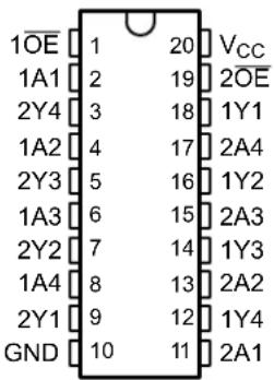
6PinConfigurationandFunctions
SN54AHC244...J OR W PACKAGE
SN74AHC244 . . . DB, DGV, DW, N, NS, OR PW PACKAGE (TOP VIEW)
text_image
1OE 1 20 Vcc 1A1 2 19 2OE 2Y4 3 18 1Y1 1A2 4 17 2A4 2Y3 5 16 1Y2 1A3 6 15 2A3 2Y2 7 14 1Y3 1A4 8 13 2A2 2Y1 9 12 1Y4 GND 10 11 2A1SN54AHC244...FK PACKAGE
(TOP VIEW)

text_image
2Y4 1A1 1OE VCC 1A2 4 3 2 1 20 19 1Y1 2Y3 5 18 1A3 6 17 2Y2 7 16 1A4 8 15 2A3 9 10 11 12 13 1Y3 2Y1 GND 2A1 1Y4 2OE 2A2PinFunctions
| PIN | I/ODESCRIPTION | ||
| NO. | NAME | ||
| 1 | 1 | I | OutputEnable1 |
| 2 | 1A1 | I | 1A1Input |
| 3 | 2Y4 | O | 2Y4Output |
| 4 | 1A2 | I | 1A2Input |
| 5 | 2Y3 | O | 2Y3Output |
| 6 | 1A3 | I | 1A3Input |
| 7 | 2Y2 | O | 2Y2Output |
| 8 | 1A4 | I | 1A4Input |
| 9 | 2Y1 | O | 2Y1Output |
| 10 | GND | — | Groundpin |
| 11 | 2A1 | I | 2A1Input |
| 12 | 1Y4 | O | 1Y4Output |
| 13 | 2A2 | I | 2A2Input |
| 14 | 1Y3 | O | 1Y3Output |
| 15 | 2A3 | I | 2A3Input |
| 16 | 1Y2 | O | 1Y2Output |
| 17 | 2A4 | I | 2A4Input |
| 18 | 1Y1 | O | 1Y1Output |
| 19 | 2 | I | OutputEnable2 |
| 20 | VCC | — | PowerPin |
7Specifications
7.1 Absolute Maximum Ratings
overoperatingfree-airtemperaturerange(unlessotherwisenoted) (1)
| MINMAXUNIT | ||||
| V_CC | Supplyvoltagerange-0.57V | |||
| V_I | Inputvoltagerange(2) | -0.57V | ||
| V_O | Outputvoltagerange(3) | -0.5V CC+0.5V | ||
| I_IK | InputclampcurrentV | I<0-20 mA | ||
| I_OK | Outputclampcurrent | V O<0orV O>V CC | ±20 | mA |
| I_O | Continuousoutputcurrent | V O=0toV CC | ±25 | mA |
| ContinuouscurrentthrougheachV CC orGND | ±50 | mA | ||
(1) Stresses beyond those listed under Absolute Maximum Ratings may cause permanent damage to the device. These are stress ratings only, and functional operation of the device at these or any other conditions beyond those indicated under Recommended Operating Conditions is not implied. Exposure to absolute-maximum-rated conditions for extended periods may affect device reliability.
(2) The input and output voltage ratings may be exceeded if the input and output current ratings are observed.
(3) ThepackagethermalimpedanceiscalculatedinaccordancewithJESD51-7.
7.2HandlingRatings
| MIN | MAX | UNIT | |||
| T_stg | Storagetemperaturerange | -65 | 150 | °C | |
| V_(ESD) | Electrostaticdischarge | Humanbodymodel(HBM),perANSI/ESDA/JEDECJS-001,all pins ^(1) | 0 | 1500 | V |
| Chargeddevicemodel(CDM),perJEDECspecification JESD22-C101,allpins ^(2) | 0 | 2000 | |||
(1) JEDEC document JEP155 states that 500-V HBM allows safe manufacturing with a standard ESD control process.
(2) JEDEC document JEP157 states that 250-V CDM allows safe manufacturing with a standard ESD control process.
7.3 Recommended Operating Conditions
overoperatingfree-airtemperaturerange(unlessotherwisenoted) ^(1)
| SN54AHC244 | SN74AHC244 | UNIT | |||||
| MIN | MAX | MIN | MAX | ||||
| V_CC | Supply voltage | 2 | 5.5 | 2 | 5.5 | V | |
| V_IH | High-levelinputvoltage | V_CC=2V | 1.5 | 1.5 | V | ||
| V_CC=3V | 2.1 | 2.1 | |||||
| V_CC=5.5V | 3.85 | 3.85 | |||||
| V_IL | Lowlevelinputvoltage | V_CC=2V | 0.5 | 0.5 | |||
| V_CC=3V | 0.9 | 0.9V | |||||
| V_CC=5.5V | 1.65 | 1.65 | |||||
| V_I | Input voltage | 0 | 5.5 | 0 | 5.5 | V | |
| V_O | Output voltage | 0 | V_CC | 0 | V_CC | V | |
| I_OH | High-leveloutputcurrent | V_CC=2V | -50 | -50 | μA | ||
| V_CC=3.3V±0.3V | -4 | -4 | mA | ||||
| V_CC=5V±0.5V | -8 | -8 | |||||
| I_OL | Lowleveloutputcurrent | V_CC=2V | 50 | 50 | μA | ||
| V_CC=3.3V±0.3V | 4 | 4 | mA | ||||
| V_CC=5V±0.5V | 8 | 8 | |||||
| t/ v | Input transition rise or fall rate | V_CC=3.3V±0.3V | 100 | 100 | ns/V | ||
| V_CC=5V±0.5V | 20 | 20 | |||||
| T_A | Operating free-air temperature | -55 | 125 | -40 | 125 | °C | |
(1) AllunusedinputsofthedevicemustbeheldatV CC orGNDtoensureproperdeviceoperation.RefertotheTlapplicationreport, Implications of Slow or Floating CMOS Inputs, literature number SCBA004.
7.4ThermalInformation
| THERMALMETRIC (1) | SN74AHCT244 | |||||||
| DBDGV | DWNNSPWUNIT | |||||||
| 20PINS20PINS20PINS20PINS20PINS20PINS | ||||||||
| R_ JA | Junction-to-ambient thermal resistance | 99.9 | 119.2 | 83.0 | 54.9 | 80.4 | 105.4 | °C/W |
| R_ JC(top) | Junction-to-case (top) thermal resistance | 61.7 | 34.5 | 48.9 | 41.7 | 46.9 | 39.5 | |
| R_ JB | Junction-to-board thermal resistance | 55.2 | 60.7 | 50.5 | 35.8 | 47.9 | 56.4 | |
| _JT | Junction-to-top characterization parameter | 22.6 | 1.2 | 21.1 | 27.9 | 19.9 | 3.1 | |
| _JB | Junction-to-board characterization parameter | 54.8 | 60.0 | 50.1 | 35.7 | 47.5 | 55.8 | |
| R_ JC(bot) | Junction-to-case (bottom) thermal resistance | n/a | n/a | n/a | n/a | n/a | n/a | |
(1) For more information about traditional and new thermal metrics, see the IC Package Thermal Metrics application report, SPRA953.
7.5 Electrical Characteristics
over recommended operating free-air temperature range (unless otherwise noted)
| PARAMETER | TESTCONDITIONS | V_cc | T_A=25°C | SN54AHC244 | SN74AHC244 | UNIT | ||||
| MIN | TYP | MAX | MIN | MAX | MIN | MAX | ||||
| V_OH | I_OH=-50μA | 2V1.9 | 21.91.9 | |||||||
| 3V2.9 | 32.92.9 | |||||||||
| 4.5V4.4 | 4.54.44.4 | V | ||||||||
| I_OH=-4 mA | 3 V | 2.58 | 2.48 | 2.48 | ||||||
| I_OH=-8 mA | 4.5 V | 3.94 | 3.8 | 3.8 | ||||||
| V_OL | I_OL=50μA | 2V | 0.10 | 10.1 | ||||||
| 3V | 0.10.1 | 0.1 | ||||||||
| 4.5V | 0.10 | 10.1 | V | |||||||
| I_OL=4mA | 3V | 0.360.5 | 0.44 | |||||||
| I_OL=8mA | 4.5V | 0.360.5 | 0.44 | |||||||
| I_I | V_I=5.5VorGND | 0Vto5.5V | ±0.1 | ±1 (1) | ±1 | μA | ||||
| I_OZ | V_O=V_CC orGND, V_I()=V_IL or V_IH | 5.5 V | ±0.25 | ±2.5 | ±2.5 | μA | ||||
| I_CC | V_I=V_CC orGND, I_O=0 | 5.5 V | 4 | 40 | 40 | μA | ||||
| C_I | V_I=V_CC or GND | 5 V | 2 | 10 | 10 | pF | ||||
| C_o | V_O=V_CC orGND | 5V | 3.5 | pF | ||||||
(1) OnproductscomplianttoMIL-PRF-38535, this parameter is not produced tested at V
cc=0V.
7.6SwitchingCharacteristics
overrecommendedoperatingfree-airtemperaturerange,V _CC=3.3V±0.3V (unlessotherwisenoted)(seeFigure3)
| PARAMETERUNIT | FROMTO(INPUT)(OUTPUT) | LOAD(OUTPUT)CAP | ACITANCE | T_A =25°CSN54AHC244SN74AHC244 | ||||||
| MINTYPMAX | MINMAX | MINMAX | ||||||||
| t_PLH | AY | C | L=15pF | 5.8(1) | 8.4(1) | 1(1) | 10(1) | 1 | 10 | |
| t_PHL | 5.8(1) | 8.4(1) | 1(1) | 10(1) | 1 | 10 | ||||
| t_PZH | Y | C_L=15pF | 6.6(1) | 10.6(1) | 1(1) | 12.5(1) | 112.5 | ns | ||
| t_PZL | 6.6(1) | 10.6(1) | 1(1) | 12.5(1) | 112.5 | |||||
| t_PHZ | Y | C_L=15pF | 5(1) | 9.7(1) | 1(1) | 11(1) | 1 | 11 | ns | |
| t_PLZ | 5(1) | 9.7(1) | 1(1) | 11(1) | 1 | 11 | ||||
| t_PLH | AY | C | L=50pF | 8.311.9 | 113.5 | 113.5 | ns | |||
| t_PHL | 8.311.9 | 113.5 | 113.5 | |||||||
| t_PZH | Y | C_L=50pF | 9.1 | 14.1 | 1 | 16 | 1 | 16 | ns | |
| t_PZL | 9.1 | 14.1 | 1 | 16 | 1 | 16 | ||||
| t_PHZ | Y | C_L=50pF | 10.3 | 14 | 1 | 16 | 1 | 16 | ns | |
| t_PLZ | 10.3 | 14 | 1 | 16 | 1 | 16 | ||||
| t_sk(o) | C_L=50pF | 1.5(2) | 1.5 | ns | ||||||
(1) OnproductscomplianttoMIL-PRF-38535,thisparameterisnotproductiontested.
(2) OnproductscomplianttoMIL-PRF-38535, thisparameterdoesnotapply.
7.7 Switching Characteristics
overrecommendedoperatingfree-airtemperatureange,V _CC=5V±0.5V (unlessotherwisenoted)(seeFigure3)
| PARAMETER | FROM(INPUT) | TO(OUTPUT) | LOADCAPACITANCE | T_A =25°C | SN54AHC244 | SN74AHC244 | UNIT | ||||
| MIN | TYP | MAX | MIN | MAX | MIN | MAX | |||||
| t_PLH | A | Y | C_L =15pF | 3.9(1) | 5.5(1) | 1(1) | 6.5(1) | 1 | 6.5 | ns | |
| t_PHL | 3.9(1) | 5.5(1) | 1(1) | 6.5(1) | 1 | 6.5 | |||||
| t_PZH | Y | C_L =15pF | 4.7(1) | 7.3(1) | 1(1) | 8.5(1) | 1 | 8.5 | ns | ||
| t_PZL | 4.7(1) | 7.3(1) | 1(1) | 8.5(1) | 1 | 8.5 | |||||
| t_PHZ | Y | C_L =15pF | 5(1) | 7.2(1) | 1(1) | 8.5(1) | 1 | 8.5 | ns | ||
| t_PLZ | 5(1) | 7.2(1) | 1(1) | 8.5(1) | 1 | 8.5 | |||||
| t_PLH | A | Y | C_L =50pF | 5.4 | 7.5 | 1 | 8.5 | 1 | 8.5 | ns | |
| t_PHL | 5.4 | 7.5 | 1 | 8.5 | 1 | 8.5 | |||||
| t_PZH | Y | C_L =50pF | 6.2 | 9.3 | 1 | 10.5 | 1 | 10.5 | ns | ||
| t_PZL | 6.2 | 9.3 | 1 | 10.5 | 1 | 10.5 | |||||
| t_PHZ | Y | C_L =50pF | 6.7 | 9.2 | 1 | 10.5 | 1 | 10.5 | ns | ||
| t_PLZ | 6.7 | 9.2 | 1 | 10.5 | 1 | 10.5 | |||||
| t_sk(o) | C_L =50pF | 1(2) | 1 | ns | |||||||
(1) OnproductscomplianttoMIL-PRF-38535,thisparameterisnotproductiontested.
(2) OnproductscomplianttoMIL-PRF-38535, thisparameterdoesnotapply.
7.8NoiseCharacteristics
$$ V _ {C C} = 5 V, C \quad_ {L} = 5 0 p F, T \quad_ {A} = 2 5 ^ {\circ} C (\text { See } ^ {(1)}) $$
| PARAMETER | SN74AHC244 | UNIT | |||
| MIN | TYP | MAX | |||
| V_OL(P) | Quiet output, maximum dynamic V_OL | 0.5 | V | ||
| V_OL(V) | Quiet output, minimum dynamic V_OL | -0.2 | V | ||
| V_OH(V) | Quiet output, minimum dynamic V_OH | 4.8 | V | ||
| V_IH(D) | High-level dynamic input voltage | 3.5 | V | ||
| V_IL(D) | Low-level dynamic input voltage | 1.5 | V | ||
(1) Characteristics are for surface-mount packages only.
7.9 Operating Characteristics
$$ V _ {C C} = 5 V, T \quad_ {A} = 2 5 ^ {\circ} C $$
| PARAMETER | TEST CONDITIONS | TYP | UNIT | |
| C_pd | Power dissipation capacitance | No load, f = 1 MHz | 8.6 | pF |
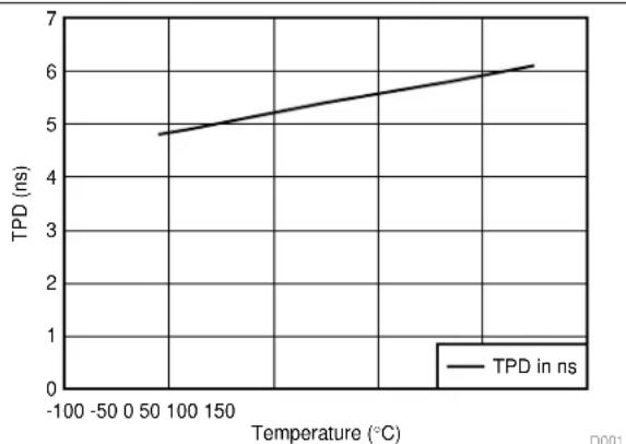
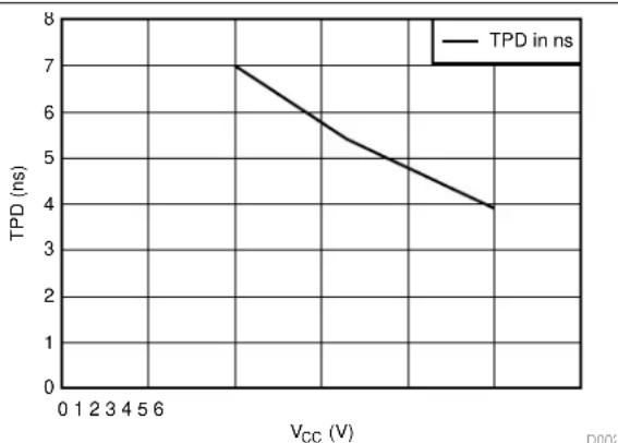
7.10 Typical Characteristics
line
| Temperature (°C) | TPD (ns) | | ---------------- | -------- | | -50 | 4.8 | | 0 | 5.0 | | 50 | 5.2 | | 100 | 5.4 | | 150 | 5.6 | | 200 | 5.8 | | 250 | 6.0 | | 300 | 6.2 |Figure 1. TPD vs Temperature
line
| Vcc (V) | TPD (ns) | | ------- | -------- | | 0 | 7 | | 6 | 4 |Figure 2. TPD vs V_cc
8ParameterMeasurementInformation
text_image
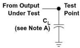
From Output Under Test Test Point CL (see Note A)LOAD CIRCUIT FOR TOTEM-POLE OUTPUTS
text_image
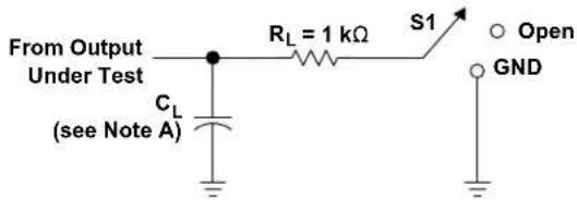
From Output Under Test CL (see Note A) RL = 1 kΩ S1 Open GNDLOAD CIRCUIT FOR 3-STATE AND OPEN-DRAIN OUTPUTS
| TEST S1 | |
| t_PLH/t_PHL | Open |
| t_PLZ/t_PZL | V_CC |
| t_PHZ/t_PZH | GND |
| Open Drain | V_CC |
text_image
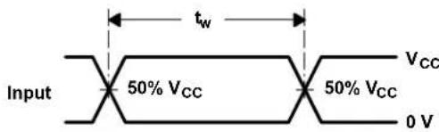
Input 50% VCC tw 50% VCC VCC 0 Vtext_image
Timing Input 50% VCC VCC 0 V tsu th Data Input 50% VCC 50% VCC VCC 0 VVOLTAGE WAVEFORMS SETUP AND HOLD TIMES
other
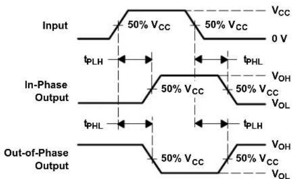
| Signal Type | Input (Vcc) | In-Phase Output (Vcc) | Out-of-Phase Output (Vcc) | | ----------------- | ----------- | --------------------- | ------------------------- | | Input | 0 V | - | - | | In-Phase Output | - | 50% | - | | Out-of-Phase Output | - | - | 50% |VOLTAGE WAVEFORMS PROPAGATION DELAY TIMES INVERTING AND NONINVERTING OUTPUTS
other
| Signal Type | Time Interval | Label | | --- | --- | --- | | Output Control | 0 V | V_CC | | Output Waveform 1 S1 at V_CC (see Note B) | 50% V_CC | t_PZL | | Output Waveform 1 S1 at V_CC (see Note B) | 50% V_CC | t_PLZ | | Output Waveform 1 S1 at V_CC (see Note B) | 50% V_CC | V_OL + 0.3 V | | Output Waveform 1 S1 at V_CC (see Note B) | 50% V_CC | V_OL | | Output Waveform 1 S1 at V_CC (see Note B) | 50% V_CC | t_PZH | | Output Waveform 2 S1 at GND (see Note B) | 0 V | V_OL - 0.3 V | | Output Waveform 2 S1 at GND (see Note B) | 50% V_CC | V_OH - 0.3 V | | Output Waveform 2 S1 at GND (see Note B) | 50% V_CC | ≈V_CC | | Output Waveform 2 S1 at GND (see Note B) | 50% V_CC | ≈V_OL + 0.3 V | | Output Waveform 2 S1 at GND (see Note B) | 50% V_CC | ≈V_OL | | Output Waveform 2 S1 at GND (see Note B) | 50% V_CC | ≈V_CC |VOLTAGE WAVEFORMS
ENABLE AND DISABLE TIMES
LOW- AND HIGH-LEVEL ENABLING
NOTES: A. C L includes probe and jig capacitance.
B. Waveform 1 is for an output with internal conditions such that the output is low except when disabled by the output control. Waveform 2 is for an output with internal conditions such that the output is high except when disabled by the output control.
C. All input pulses are supplied by generators having the following characteristics: PRR ≤ 1 MHz, Z O = 50 Ω, t ≤ 3 ns, t _f ≤ 3 ns.
D. The outputs are measured one at a time with one input transition per measurement.
E. All parameters and waveforms are not applicable to all devices.
Figure3.LoadCircuitandVoltageWaveforms
9DetailedDescription
9.1 Overview
TheSNx4AHC244devicesareorganizedastwo4-bitbuffers/linedriverswithseparateoutput-enable(OE) inputs.WhenOEislow,thedevicepassesdatafromtheAinputstotheYoutputs.WhenOEishigh,theoutputs areinthehigh-impedancestate.Toensurethehigh-impedancestateduringpoweruporpowerdown,OE shouldbetiedtoV CC throughapullupresistor;themimumvalueoftheresistorisdeterminedbythecurrent-sinkingcapabilityofthedriver.
9.2 FunctionalBlockDiagram
flowchart
graph TD
    A["1OE"] --> B["NOT Gate"]
    C["1A1"] --> D["AND Gate"]
    E["1A2"] --> F["AND Gate"]
    G["1A3"] --> H["AND Gate"]
    I["1A4"] --> J["AND Gate"]
    B --> K["1Y1"]
    D --> L["1Y2"]
    F --> M["1Y3"]
    H --> N["1Y4"]
    J --> O["1Y4"]
flowchart
graph TD
    A["2OE"] --> B["19"]
    C["2A1"] --> D["11"]
    E["2A2"] --> F["13"]
    G["2A3"] --> H["15"]
    I["2A4"] --> J["17"]
    B --> K["9"]
    D --> L["7"]
    F --> M["5"]
    H --> N["3"]
    J --> O["2Y1"]
    K --> P["2Y2"]
    L --> Q["2Y3"]
    M --> R["2Y4"]
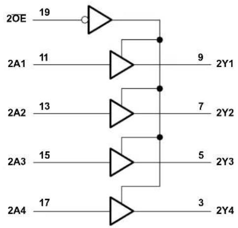
Figure4.LogicDiagram(PositiveLogic)
9.3FeatureDescription
• V_cc isoptimizedat5V
- Allowsdownvoltagetranslation
- InputsacceptV _IH levelsof5.5V
- Slowedgeratesminimizeoutputringing
9.4DeviceFunctionalModes
Table1.FunctionTable (Each4-BitBuffer/Driver)
| INPUTS | OUTPUT Y | |
| A | ||
| L | H | H |
| L | L | L |
| H | X | Z |
10ApplicationandImplementation
10.1 Application Information
TheSNx4AHC244isalowdriveCMOSdevicethatcanbeusedforamultitudeofbusinterfacetypeapplications whereoutputringingisaconcern. Thelowdriveandslowedgerateswillminimizeovershootandundershooton theoutputs. Theinputscanexceptvoltagesto5.5VatanyvalidV CC makingitidealfordowntranslation.
10.2 Typical Application
flowchart
graph TD
    A["Regulated 5 V"] --> B["μC or System Logic"]
    B --> C["OE"]
    B --> D["A1"]
    B --> E["A4"]
    B --> F["GND"]
    C --> G["Vcc"]
    D --> H["Y1"]
    E --> I["Y4"]
    F --> J["μC System Logic LEDs"]
Figure5.TypicalApplicationDiagram
10.2.1 Design Requirements
This device uses CMOS technology and has balanced output drive. Careshould be takento avoid bus contention because it can drive current that would exceed maximum limits. The high drivewill also create fast edges into light loadssorouting and load condition should be considered to prevent ringing.
10.2.2 Detailed Design Procedure
•Recommendedinputconditions
-Specifiedhighandlowlevels.See(V IH and V IL )inRecommendedOperatingConditions.
-Inputsareovervoltagetolerantallowingthemtogoashighas5.5VatanyvalidV cc
- Recommendoutputconditions
-Loadcurrentsshouldnotexceed25mAperoutputand50mAtotalforthepart
-OutputsshouldnotbepulledaboveV cc
TypicalApplication(continued)
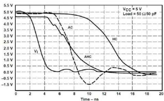
10.2.3 ApplicationCurves
line
| Time (ns) | V_I | AC | AHC | HC | |-----------|--------|--------|--------|--------| | 0 | 5.0 V | 5.0 V | 5.0 V | 5.0 V | | 2 | 4.8 V | 4.9 V | 4.8 V | 4.9 V | | 4 | 0.0 V | 4.7 V | 4.5 V | 4.7 V | | 6 | -0.5 V | 3.5 V | 3.0 V | 3.5 V | | 8 | -0.5 V | 2.0 V | 1.5 V | 2.0 V | | 10 | -0.5 V | -1.5 V | -0.5 V | -1.5 V | | 12 | -0.5 V | -0.5 V | -0.5 V | -0.5 V | | 14 | -0.5 V | -0.5 V | -0.5 V | -0.5 V | | 16 | -0.5 V | -0.5 V | -0.5 V | -0.5 V | | 18 | -0.5 V | -0.5 V | -0.5 V | -0.5 V | | 20 | -0.5 V | -0.5 V | -0.5 V | -0.5 V |Figure6.SwitchingCharacteristicsComparison
11PowerSupplyRecommendations
The powersupply can be any voltage between the MIN and MAX supply voltage, operating located in the Recommended Operating Condition stable.
EachVCCpinshouldhaveagoodbypasscapacitortopreventpowerdisturbance. Fordeviceswithasingle supply, 0.1 μf is recommended; if there are multiple VCC pins, then 0.01 μf or 0.022 μf is recommended for each power pin. It is acceptable to parallel multiple bypass caps to reject different frequencies of noise. A 0.1 μf and a 1 μf are commonly used in parallel. The bypass capacitor should be installed as close to the power pin as possibleforbestresults.
12Layout
12.1 LayoutGuidelines
When using multiple-bit logic devices, input should never float.
Inmanycases, functionsorpartsoffunctionsofdigitallogicdevicesareunused,forexample,whenonlytwo inputsofatriple-inputANDgateareusedoronly3ofthe4buffergatesareused.Suchinputpinsshouldnot beleftunconnectedbecausetheundefinedvoltagesattheoutsideconnectionsresultinundefined operational states. Figure 7 specifies the rules that must be observed under all circumstances. All unused inputs of digital logic devices must be connected to a high or low bias to prevent them from floating. The logiclevelthatshouldbeappliedtoanyparticularunusedinputdependsonthefunctionofthedevice. Generally they will be tied to GND or V_CC , whichever makes more sense or is more convenient. It is generallyacceptabletofloatoutputs,unlessthepartisatransceiver.Ifthetransceiverhasanoutputenable pin,itwilldisabletheoutputsectionofthepartwhenasserted.Thiswillnotdisabletheinputsectionofthe I/Os,sotheycannotfloatwhendisabled.
12.2LayoutExample

text_image
Vcc Unused Input Input Output
text_image
Input Unused Input OutputFigure7.LayoutDiagram
13DeviceandDocumentationSupport
13.1 RelatedLinks
Thetablebelowlistsquickaccesslinks. Categories include technical documents, support and community resources, tools and software, and quick access to sample or buy.
Table2.RelatedLinks
| PARTSPRODU | CTFOLDERSAMPLE& | BUY | TECHNICALTOOLS&SUPPORT& DOCUMENTSSOFTWARECOMMUNITY | ||
| SN54AHC244 | Click here | Click here | Click here | Click here | Click here |
| SN74AHC244 | Click here | Click here | Click here | Click here | Click here |
13.2 Trademarks
Alltrademarksarethepropertyoftheirrespectiveowners.
13.3 Electrostatic Discharge Caution

These devices have limited built-in ESD protection. The leads should be shorted together or the device placed in conductive foam duringstorageorhandlingtopreventelectrostaticdamagetotheMOSgates.
13.4 Glossary
SLYZ022 — TIGlossary.
This glossarylistsandexplainsterms,acronyms,anddefinitions.
14Mechanical, Packaging, and Orderable Information
The following pages include mechanical, packaging, and orderable information. This information is the most current data available for the designated devices. This data is subject to change without notice and revision of this document. For browser-based versions of this datasheet, refertotheleft-handnavigation.
PACKAGING INFORMATION
| Orderable Device Status(1) | Package Type | Package Drawing | Pins | Package Qty | Eco Plan(2) | Lead finish/ Ball material(6) | MSL Peak Temp(3) | Op Temp (°C) | Device Marking(4,5) | Samples | |
| 5962-9678201Q2A ACTIVE LCCC FK 20 1 Non-RoHS | & Green | SNPB N / A for Pkg Type -55 to 125 5962- | 9678201Q2A SNJ54AHC 244FK | Samples | |||||||
| 5962-9678201QRA ACTIVE CDIP J 20 1 Non-RoHS | & Green | SNPB N / A for Pkg Type -55 to 125 5962-9678201QR | A SNJ54AHC244J | Samples | |||||||
| 5962-9678201QSA ACTIVE CFP W 20 1 Non-RoHS | & Green | SNPB N / A for Pkg Type -55 to 125 5962-9678201QS | A SNJ54AHC244W | Samples | |||||||
| 5962-9678201VRA ACTIVE CDIP J 20 1 Non-RoHS | & Green | SNPB N / A for Pkg Type -55 to 125 5962-9678201VR | A SNV54AHC244J | Samples | |||||||
| 5962-9678201VSA ACTIVE CFP | W 20 1 Non-RoHS | & Green | SNPB N / A for Pkg Type -55 to 125 5962-9678201VS | A SNV54AHC244W | Samples | ||||||
| SN74AHC244DBR | ACTIVE | SSOP | DB | 20 | 2000 | RoHS & Green | NIPDAU | Level-1-260C-UNLIM | -40 to 125 | HA244 | Samples |
| SN74AHC244DBRE4 | ACTIVE | SSOP | DB | 20 | 2000 | RoHS & Green | NIPDAU | Level-1-260C-UNLIM | -40 to 125 | HA244 | Samples |
| SN74AHC244DGVR | ACTIVE | TVSOP | DGV | 20 | 2000 | RoHS & Green | NIPDAU | Level-1-260C-UNLIM | -40 to 125 | HA244 | Samples |
| SN74AHC244DW | ACTIVE | SOIC | DW | 20 | 25 | RoHS & Green | NIPDAU | Level-1-260C-UNLIM | -40 to 125 | AHC244 | Samples |
| SN74AHC244DWE4 | ACTIVE | SOIC | DW | 20 | 25 | RoHS & Green | NIPDAU | Level-1-260C-UNLIM | -40 to 125 | AHC244 | Samples |
| SN74AHC244DWR | ACTIVE | SOIC | DW | 20 | 2000 | RoHS & Green | NIPDAU | Level-1-260C-UNLIM | -40 to 125 | AHC244 | Samples |
| SN74AHC244DWRG4 | ACTIVE | SOIC | DW | 20 | 2000 | RoHS & Green | NIPDAU | Level-1-260C-UNLIM | -40 to 125 | AHC244 | Samples |
| SN74AHC244N | ACTIVE | PDIP | N | 20 | 20 | RoHS & Non-Green | NIPDAU | N / A for Pkg Type -40 to 125 SN74AHC244N | Samples | ||
| SN74AHC244NSR | ACTIVE | SO | NS | 20 | 2000 | RoHS & Green | NIPDAU | Level-1-260C-UNLIM | -40 to 125 | AHC244 | Samples |
| SN74AHC244PW | ACTIVE | TSSOP | PW | 20 | 70 | RoHS & Green | NIPDAU | Level-1-260C-UNLIM | -40 to 125 | HA244 | Samples |
| SN74AHC244PWG4 | ACTIVE | TSSOP | PW | 20 | 70 | RoHS & Green | NIPDAU | Level-1-260C-UNLIM | -40 to 125 | HA244 | Samples |
Addendum-Page 1
| Orderable Device Status | (1) | Package Type | Package Drawing | Pins | Package Qty | Eco Plan (2) | Lead finish/ Ball material (6) | MSL Peak Temp (3) | Op Temp (°C) | Device Marking (4,5) | Samples |
| SN74AHC244PWR ACTIVE TSSOP PW 20 2000 RoHS & Green NIPDAU | SN Level-1-260C-UNLIM -40 to 85 HA244 | Samples | ||||||||||
| SN74AHC244PWRE4 | ACTIVE | TSSOP | PW | 20 | 2000 | RoHS & Green | NIPDAU | Level-1-260C-UNLIM | -40 to 125 | HA244 | Samples |
| SN74AHC244PWRG4 | ACTIVE | TSSOP | PW | 20 | 2000 | RoHS & Green | NIPDAU | Level-1-260C-UNLIM | -40 to 125 | HA244 | Samples |
| SNJ54AHC244FK | ACTIVE | LCCC | FK | 20 | 1 | Non-RoHS & Green | SNPB N / A for Pkg Type | -55 to 125 | 5962- | 9678201Q2A SNJ54AHC 244FK | Samples |
| SNJ54AHC244J | ACTIVE | CDIP | J | 20 | 1 | Non-RoHS & Green | SNPB N / A for Pkg Type | -55 to 125 | 5962-9678201QR A SNJ54AHC244J | Samples | |
| SNJ54AHC244W ACTIVE | CFP W | 20 1 | Non-RoHS | & Green | SNPB N / A for Pkg Type | -55 to 125 | 5962-9678201QS A SNJ54AHC244W | Samples | |||
(1) The marketing status values are defined as follows:
ACTIVE: Product device recommended for new designs.
LIFEBUY: TI has announced that the device will be discontinued, and a lifetime-buy period is in effect.
NRND: Not recommended for new designs. Device is in production to support existing customers, but TI does not recommend using this part in a new design.
PREVIEW: Device has been announced but is not in production. Samples may or may not be available.
OBSOLETE: TI has discontinued the production of the device.
(2) RoHS: TI defines "RoHS" to mean semiconductor products that are compliant with the current EU RoHS requirements for all 10 RoHS substances, including the requirement that RoHS substance do not exceed 0.1% by weight in homogeneous materials. Where designed to be soldered at high temperatures, "RoHS" products are suitable for use in specified lead-free processes. TI may reference these types of products as "Pb-Free".
RoHS Exempt: TI defines "RoHS Exempt" to mean products that contain lead but are compliant with EU RoHS pursuant to a specific EU RoHS exemption.
Green: TI defines "Green" to mean the content of Chlorine (Cl) and Bromine (Br) based flame retardants meet JS709B low halogen requirements of <=1000ppm threshold. Antimony trioxide based flame retardants must also meet the <=1000ppm threshold requirement.
(3) MSL, Peak Temp. - The Moisture Sensitivity Level rating according to the JEDEC industry standard classifications, and peak solder temperature.
(4) There may be additional marking, which relates to the logo, the lot trace code information, or the environmental category on the device.
(5) Multiple Device Markings will be Inside parentheses. Only one Device Marking contained in parentheses and separated by a "\~" will appear on a device. If a line is Indented then it is a continuation of the previous line and the two combined represent the entire Device Marking for that device.
(6) Lead finish/Ball material - Orderable Devices may have multiple material finish options. Finish options are separated by a vertical ruled line. Lead finish/Ball material values may wrap to two lines if the finish value exceeds the maximum column width.
Important Information and Disclaimer: The information provided on this page represents TI's knowledge and belief as of the date that it is provided. TI bases its knowledge and belief on information provided by third parties, and makes no representation or warranty as to the accuracy of such information. Efforts are underway to better integrate information from third parties. TI has taken and continues to take reasonable steps to provide representative and accurate information but may not have conducted destructive testing or chemical analysis on incoming materials and chemicals. TI and TI suppliers consider certain information to be proprietary, and thus CAS numbers and other limited information may not be available for release.
In no event shall TI's liability arising out of such information exceed the total purchase price of the TI part(s) at issue in this document sold by TI to Customer on an annual basis.
OTHER QUALIFIED VERSIONS OF SN54AHC244, SN54AHC244-SP, SN74AHC244 :
• Catalog : SN74AHC244, SN54AHC244
• Automotive : SN74AHC244-Q1, SN74AHC244-Q1
• Enhanced Product : SN74AHC244-EP, SN74AHC244-EP
• Military : SN54AHC244
• Space : SN54AHC244-SP
NOTE: Qualified Version Definitions:
• Catalog - TI's standard catalog product
• Automotive - Q100 devices qualified for high-reliability automotive applications targeting zero defects
• Enhanced Product - Supports Defense, Aerospace and Medical Applications
• Military - QML certified for Military and Defense Applications
• Space - Radiation tolerant, ceramic packaging and qualified for use in Space-based application
TAPE AND REEL INFORMATION
*All dimensions are nominal
| Device Package | Type | Package Drawing | Pins | SPQ Reel | Diameter (mm) | Reel Width W1 (mm) | A0 (mm) | B0 (mm) | K0 (mm) | P1 (mm) | W (mm) | Pin1 Quadrant |
| SN74AHC244DBR SSOP DB 20 | 2000 330.0 | 16.4 | 8.2 7.5 2.5 | 12.0 16.0 | Q1 | |||||||
| SN74AHC244DGVR TVSOP DGV | 20 2000 3 | 30.0 1 | 2.4 6.9 5.6 | 1.6 8.0 12.0 | Q1 | |||||||
| SN74AHC244DWR SOIC DW 20 | 2000 330.0 | 24.4 | 10.9 13.3 | 2.7 12.0 24.0 | Q1 | |||||||
| SN74AHC244NSR | SO | NS 20 | 2000 330.0 24.4 | 8.4 13.0 25 | 12.0 24.0 | Q1 | ||||||
| SN74AHC244PWR | TSSOP PW | 20 | 2000 330.0 16.4 | 6.95 7.0 | 1.4 8.0 16.0 | Q1 | ||||||
| SN74AHC244PWR | TSSOP PW | 20 | 2000 330.0 16.4 | 6.95 7.1 | 1.6 8.0 16.0 | Q1 | ||||||
| SN74AHC244PWRG4 | TSSOP | PW | 20 | 2000 | 330.0 | 16.4 | 6.95 | 7.0 | 1.4 | 8.0 | 16.0 | Q1 |
text_image
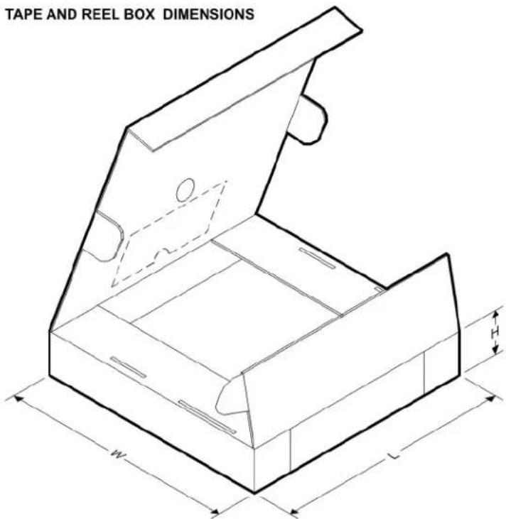
TAPE AND REEL BOX DIMENSIONS W L*All dimensions are nominal
| Device | Package Type | Package Drawing | Pins | SPQ | Length (mm) | Width (mm) | Height (mm) |
| SN74AHC244DBR SSOP DB 20 2000 853 | 0 449.0 35.0 | ||||||
| SN74AHC244DGVR TVSOP DGV 20 2000 | 853.0 449.0 35.0 | ||||||
| SN74AHC244DWR SO C DW 20 2000 367 | 0 367.0 45.0 | ||||||
| SN74AHC244NSR SO NS | 20 2000 367.0 367.0 45.0 | ||||||
| SN74AHC244PWR | TSSOP | PW | 20 | 2000 | 853.0 | 449.0 | 35.0 |
| SN74AHC244PWR | TSSOP | PW | 20 | 2000 | 364.0 | 364.0 | 27.0 |
| SN74AHC244PWRG4 | TSSOP | PW | 20 | 2000 | 367.0 | 367.0 | 38.0 |
TUBE
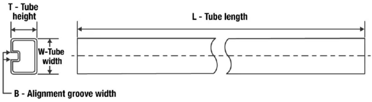
text_image
T - Tube height L - Tube length W-Tube width B - Alignment groove width*All dimensions are nominal
| Device | Package Name | Package Type | Pins | SPQ | L (mm) | W (mm) | T (μm) | B (mm) |
| 5962-9678201Q2A FK | CCC 20 1 506.98 | 12.06 2030 NA | ||||||
| 5962-9678201VSA W CFP | 20 1 506.98 | 26.16 6220 NA | ||||||
| SN74AHC244DW | DW | SOIC | 20 | 25 | 507 | 12.83 | 5080 | 6.6 |
| SN74AHC244DWE4 | DW | SOIC | 20 | 25 | 507 | 12.83 | 5080 | 6.6 |
| SN74AHC244N | N | PDIP | 20 | 20 | 506 | 13.97 | 11230 | 4.32 |
| SN74AHC244PW | PW | TSSOP | 20 | 70 | 530 | 10.2 | 3600 | 3.5 |
| SN74AHC244PWG4 | PW | TSSOP | 20 | 70 | 530 | 10.2 | 3600 | 3.5 |
| SNJ54AHC244FK FK | CCC 20 1 506.98 | 12.06 2030 NA |
W (R-GDFP-F20)
CERAMIC DUAL FLATPACK
other
| Dimension | Value | | ----------------- | ------- | | Base and Seating Plane | 0.300 | | Base and Seating Plane | 0.245 | | Base and Seating Plane | 0.320 | | Base and Seating Plane | 0.540 | | Base and Seating Plane | 1 | | Base and Seating Plane | 20 | | Base and Seating Plane | 11 | | Base and Seating Plane | 10 | | Base and Seating Plane | 11 | | Base and Seating Plane | 11 | | Base and Seating Plane | 11 | | Base and Seating Plane | 11 | | Base and Seating Plane | 11 | | Base and Seating Plane | 11 | | Base and Seating Plane | 11 | | Base and Seating Plane | 11 | | Base and Seating Plane | 11 | | 0.045 (1,14) | 0.045 | | 0.026 (0,66) | 0.026 | | 0.100 (2,45) | 0.100 | | 0.045 (1,14) | 0.045 | | 0.320 (8,13) MAX | 0.320 | | 0.009 (0,23) | 0.009 | | 0.004 (0,10) | 0.004 | | 0.540 (13,72) MAX | 0.540 | | 0.370 (9,40) | 0.370 | | 0.250 (6,35) | 0.250 | | 0.022 (0,56) | 0.022 | | 0.015 (0,38) | 0.015 | | 0.050 (1,27) | 0.050 | | 0.370 (9,40) | 0.370 | | 0.250 (6,35) | 0.250 | | 4040180–4/F | 4 |NOTES: A. All linear dimensions are in inches (millimeters).
B. This drawing is subject to change without notice.
C. This package can be hermetically sealed with a ceramic lid using glass frit.
D. Index point is provided on cap for terminal identification only.
E. Falls within Mil-Std 1835 GDFP2-F20
SMALL OUTLINE PACKAGE

text_image
A 6.6 TYP 6.2 PIN 1 INDEX AREA 1 20 18X 0.65 6.6 6.4 NOTE 3 2X 5.85 10 11 20X 0.30 0.19 B 4.5 4.3 NOTE 4 ⊕ 0.1@ A B
text_image
C SEATING PLANE 0.1 C 1.2 MAX
text_image
SEE DETAIL A (0.15) TYP
text_image
GAGE PLANE 0.25 0.15 0.05 0°-8° 0.75 0.50 DETAIL A TYPICAL4220206/A 02/2017
NOTES:
- All linear dimensions are in millimeters. Any dimensions in parenthesis are for reference only. Dimensioning and tolerancing per ASME Y14.5M.
- This drawing is subject to change without notice.
- This dimension does not include mold flash, protrusions, or gate burrs. Mold flash, protrusions, or gate burrs shall not exceed 0.15 mm per side.
- This dimension does not include interlead flash. Interlead flash shall not exceed 0.25 mm per side.
- Reference JEDEC registration MO-153.
SMALL OUTLINE PACKAGE
text_image
20X (1.5) 1 20X (0.45) 18X (0.65) 10 (5.8) SYMM (R0.05) TYP 20 SYMM 11LAND PATTERN EXAMPLE
EXPOSED METAL SHOWN
SCALE: 10X
text_image
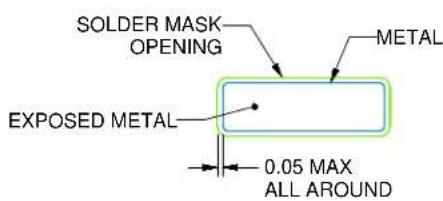
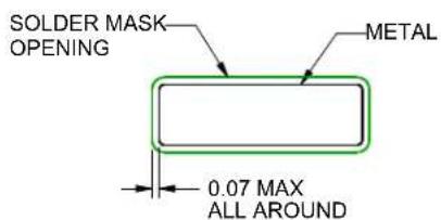
SOLDER MASK OPENING METAL EXPOSED METAL 0.05 MAX ALL AROUNDNON-SOLDER MASK DEFINED (PREFERRED)
text_image
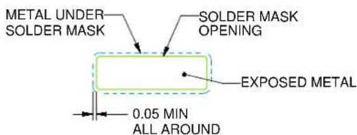
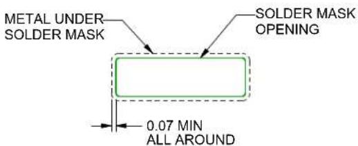
METAL UNDER SOLDER MASK SOLDER MASK OPENING EXPOSED METAL 0.05 MIN ALL AROUNDSOLDER MASK DETAILS
4220206/A 02/2017
NOTES: (continued)
- Publication IPC-7351 may have alternate designs.
- Solder mask tolerances between and around signal pads can vary based on board fabrication site.
SMALL OUTLINE PACKAGE

text_image
20X (1.5) 1 20X (0.45) SYMM (R0.05) TYP 20 18X (0.65) SYMM 10 (5.8) 11SOLDER PASTE EXAMPLE
BASED ON 0.125 mm THICK STENCIL
SCALE: 10X
4220206/A 02/2017
NOTES: (continued)
- Laser cutting apertures with trapezoidal walls and rounded corners may offer better paste release. IPC-7525 may have alternate design recommendations.
- Board assembly site may have different recommendations for stencil design.
PW (R-PDSO-G20)
Example Board Layout
text_image
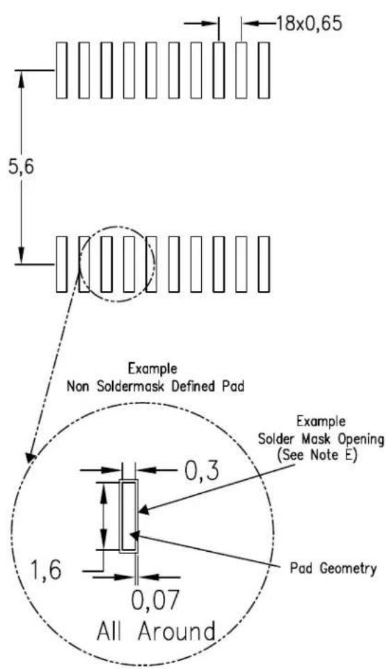
18x0,65 5,6 Example Non Soldermask Defined Pad Example Solder Mask Opening (See Note E) 0,3 1,6 0,07 Pad Geometry All AroundBased on a stencil thickness of .127mm (.005inch).

text_image
20x0,25 1,55 5,6 18x0,654211284-5/G 08/15
NOTES:
A. All linear dimensions are in millimeters.
B. This drawing is subject to change without notice.
C. Publication IPC-7351 is recommended for alternate design.
D. Laser cutting apertures with trapezoidal walls and also rounding corners will offer better paste release. Customers should contact their board assembly site for stencil design recommendations. Refer to IPC-7525 for other stencil recommendations.
E. Customers should contact their board fabrication site for solder mask tolerances between and around signal pads.
FK (S-CQCC-N**)
28 TERMINAL SHOWN
LEADLESS CERAMIC CHIP CARRIER
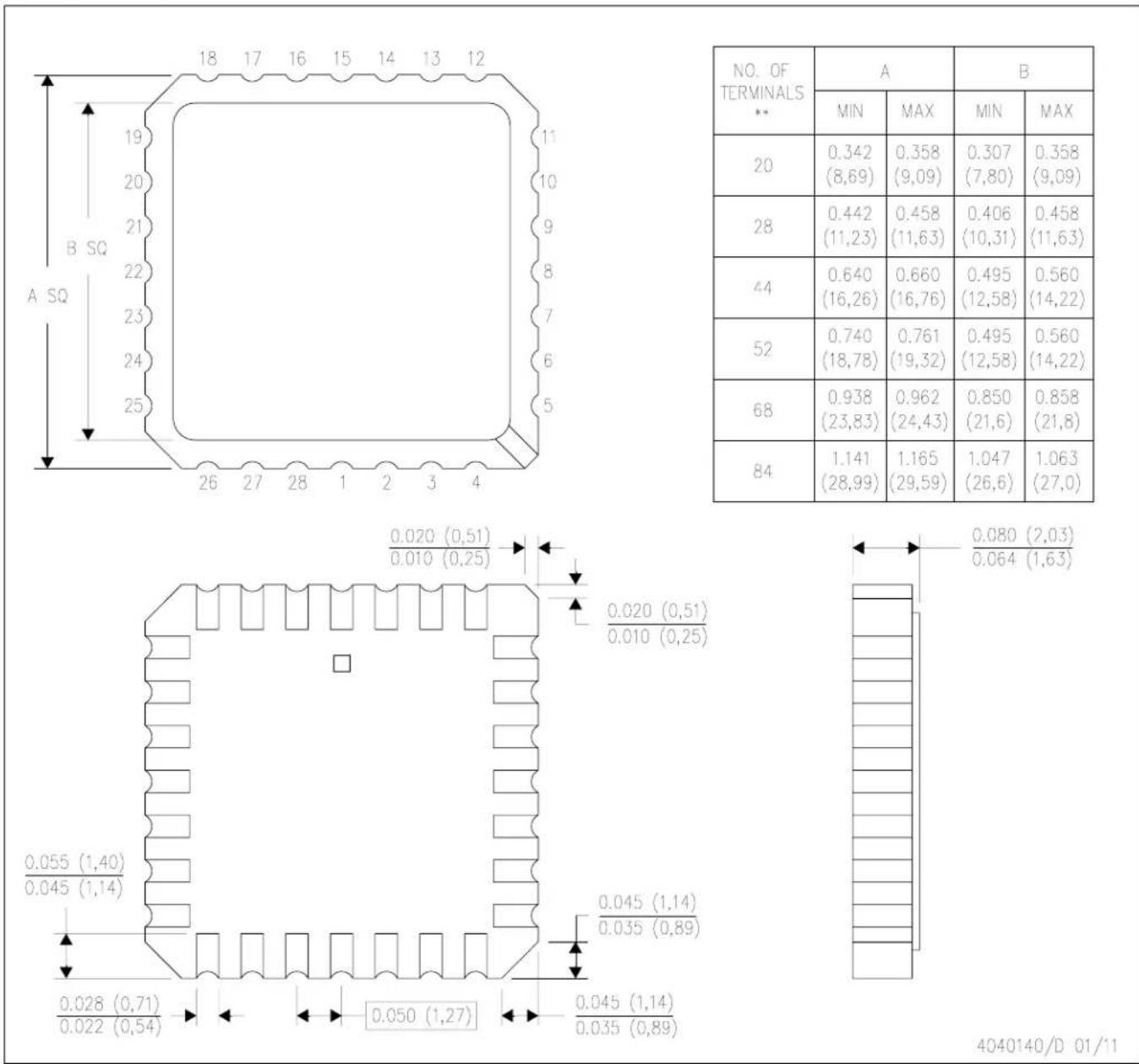
| NO. OF TERMINALS** | A | B | ||
| MIN | MAX | MIN | MAX | |
| 20 | 0.342(8,69) | 0.358(9,09) | 0.307(7,80) | 0.358(9,09) |
| 28 | 0.442(11,23) | 0.458(11,63) | 0.406(10,31) | 0.458(11,63) |
| 44 | 0.640(16,26) | 0.660(16,76) | 0.495(12,58) | 0.560(14,22) |
| 52 | 0.740(18,78) | 0.761(19,32) | 0.495(12,58) | 0.560(14,22) |
| 68 | 0.938(23,83) | 0.962(24,43) | 0.850(21,6) | 0.858(21,8) |
| 84 | 1.141(28,99) | 1.165(29,59) | 1.047(26,6) | 1.063(27,0) |
4040140/D 01/11
NOTES: A. All linear dimensions are in inches (millimeters).
B. This drawing is subject to change without notice.
C. This package can be hermetically sealed with a metal lid.
D. Falls within JEDEC MS-004
SMALL OUTLINE PACKAGE

text_image
A 8.2 7.4 TYP PIN 1 INDEX AREA 1 20 18X 0.65 7.5 6.9 NOTE 3 2X 5.85 10 11 20X 0.38 0.22 B 5.6 5.0 NOTE 4 ⊕ 0.1@ A B
text_image
C 0.1 C SEATING PLANE
text_image
SEE DETAIL A (0.15) TYP
text_image
GAGE PLANE 0.25 0° -8° 0.95 0.55 2 MAX 0.05 MINDETAIL A TYPICAL
4214851/B 08/2019
NOTES:
- All linear dimensions are in millimeters. Any dimensions in parenthesis are for reference only. Dimensioning and tolerancing per ASME Y14.5M.
- This drawing is subject to change without notice.
- This dimension does not include mold flash, protrusions, or gate burrs. Mold flash, protrusions, or gate burrs shall not exceed 0.15 mm per side.
- This dimension does not include interlead flash. Interlead flash shall not exceed 0.25 mm per side.
- Reference JEDEC registration MO-150.
SMALL OUTLINE PACKAGE
text_image
20X (1.85) SYMM (0.45) 1 20X 18X (0.65) 10 (7) R0.05 TYP 20 SYMM 11LAND PATTERN EXAMPLE
EXPOSED METAL SHOWN
SCALE: 10X
text_image
SOLDER MASK OPENING METAL EXPOSED METAL 0.07 MAX ALL AROUNDNON-SOLDER MASK DEFINED (PREFERRED)
text_image
METAL UNDER SOLDER MASK SOLDER MASK OPENING EXPOSED METAL 0.07 MIN ALL AROUNDSOLDER MASK DETAILS
4214851/B 08/2019
NOTES: (continued)
- Publication IPC-7351 may have alternate designs.
- Solder mask tolerances between and around signal pads can vary based on board fabrication site.
SMALL OUTLINE PACKAGE

text_image
20X (1.85) SYMM (0.45) 20X 1 18X (0.65) 10 (7) (R0.05) TYP 20 SYMM 11SOLDER PASTE EXAMPLE
BASED ON 0.125 mm THICK STENCIL
SCALE: 10X
4214851/B 08/2019
NOTES: (continued)
- Laser cutting apertures with trapezoidal walls and rounded corners may offer better paste release. IPC-7525 may have alternate design recommendations.
- Board assembly site may have different recommendations for stencil design.
MECHANICAL DATA
NS (R-PDSO-G\*\*)
PLASTIC SMALL-OUTLINE PACKAGE
14-PINS SHOWN

text_image
1,27 14 0,51 0,35 Ø 0,25① 8 5,60 5,00 8,20 7,40 1 7 A
text_image
0,15 NOM Gage Plane 0,25 0°-10° 1,05 0,55
text_image
2,00 MAX 0,15 0,05
text_image
Seating Plane 0.10| DIM\PINS ** | 14 | 16 | 20 | 24 |
| A MAX | 10,50 | 10,50 | 12,90 | 15,30 |
| A MIN | 9,90 | 9,90 | 12,30 | 14,70 |
4040062/C 03/03
NOTES: A. All linear dimensions are in millimeters.
B. This drawing is subject to change without notice.
C. Body dimensions do not include mold flash or protrusion, not to exceed 0,15.

text_image
B 14 8 C 1 0.065 (1,65) 0.045 (1,14)| PINS **DIM | 14 | 16 | 18 | 20 |
| A | 0.300(7,62)BSC | 0.300(7,62)BSC | 0.300(7,62)BSC | 0.300(7,62)BSC |
| B MAX | 0.785(19,94) | .840(21,34) | 0.960(24,38) | 1.060(26,92) |
| B MIN | — | — | — | — |
| C MAX | 0.300(7,62) | 0.300(7,62) | 0.310(7,87) | 0.300(7,62) |
| C MIN | 0.245(6,22) | 0.245(6,22) | 0.220(5,59) | 0.245(6,22) |
text_image
0.005 (0,13) MIN 0.060 (1,52) 0.015 (0,38) 0.200 (5,08) MAX Seating Plane 0.130 (3,30) MIN 0.026 (0,66) 0.014 (0,36) 0.100 (2,54) 0.014 (0,36) 0.008 (0,20) A 0°-15°4040083/F 03/03
NOTES:
A. All linear dimensions are in inches (millimeters).
B. This drawing is subject to change without notice.
C. This package is hermetically sealed with a ceramic lid using glass frit.
D. Index point is provided on cap for terminal identification only on press ceramic glass frit seal only.
E. Falls within MIL STD 1835 GDIP1-T14, GDIP1-T16, GDIP1-T18 and GDIP1-T20.
DGV (R-PDSO-G\*\*) PLASTIC SMALL-OUTLINE
24 PINS SHOWN
| DIM\PINS ** | 14 | 20 | 382416 | 48 | 56 | ||
| A MAX | 3,70 | 5,10 | 5,103,70 | 7,90 | 9,80 | 11,40 | |
| A MIN | 3,50 | 3,50 | 4,90 | 4,90 | 7,70 | 9,60 | 11,20 |
4073251/E 08/00
NOTES: A. All linear dimensions are in millimeters.
B. This drawing is subject to change without notice.
C. Body dimensions do not include mold flash or protrusion, not to exceed 0.15 per side.
D. Falls within JEDEC: 24/48 Pins - MO-153
14/16/20/56 Pins - MO-194
N (R-PDIP-T\*\*)
16 PINS SHOWN
PLASTIC DUAL-IN-LINE PACKAGE
text_image
A 16 9 0.260 (6,60) 0.240 (6,10) 1 8 0.070 (1,78) 0.045 (1,14)C
| DIM\PINS ** | 14 | 16 | 18 | 20 |
| A MAX | 0.775(19,69) | 0.775(19,69) | 0.920(23,37) | 1.060(26,92) |
| A MIN | 0.745(18,92) | 0.745(18,92) | 0.850(21,59) | 0.940(23,88) |
| MS-001VARIATION | AA | BB | AC | AD |

text_image
0.045 (1,14) 0.030 (0,76) D 0.020 (0,51) MIN 0.200 (5,08) MAX Seating Plane 0.125 (3,18) MIN 0.100 (2,54) 0.021 (0,53) 0.015 (0,38) ⊕ 0.010 (0,25) M 14/18 Pin Only 20 Pin vendor opt
text_image
0.325 (8,26) 0.300 (7,62) 0.015 (0,38) Gauge Plane 0.010 (0,25) NOM 0.430 (10,92) MAX4040049/E 12/2002
NOTES: A. All linear dimensions are in inches (millimeters).
B. This drawing is subject to change without notice.
C Falls within JEDEC MS-001, except 18 and 20 pin minimum body length (Dim A).
The 20 pin end lead shoulder width is a vendor option, either half or full width.
SOIC
4220724/A 05/2016
NOTES:
- All linear dimensions are in millimeters. Dimensions in parenthesis are for reference only. Dimensioning and tolerancing per ASME Y14.5M.
- This drawing is subject to change without notice.
- This dimension does not include mold flash, protrusions, or gate burrs. Mold flash, protrusions, or gate burrs shall not exceed 0.15 mm per side.
- This dimension does not include interlead flash. Interlead flash shall not exceed 0.43 mm per side.
- Reference JEDEC registration MS-013.
SOIC

text_image
20X (2) 1 20X (0.6) 18X (1.27) (R0.05) TYP 10 SYMM 20 SYMM 11 (9.3)LAND PATTERN EXAMPLE SCALE:6X
text_image
SOLDER MASK OPENING METAL 0.07 MAX ALL AROUNDNON SOLDER MASK DEFINED
text_image
METAL UNDER SOLDER MASK SOLDER MASK OPENING 0.07 MIN ALL AROUNDSOLDER MASK
DEFINED
SOLDER MASK DETAILS
4220724/A 05/2016
NOTES: (continued)
- Publication IPC-7351 may have alternate designs.
- Solder mask tolerances between and around signal pads can vary based on board fabrication site.
SOIC

text_image
20X (2) 1 20X (0.6) 18X (1.27) SYMM 20 SYMM 10 (9.3) 11SOLDER PASTE EXAMPLE
BASED ON 0.125 mm THICK STENCIL
SCALE:6X
4220724/A 05/2016
NOTES: (continued)
- Laser cutting apertures with trapezoidal walls and rounded corners may offer better paste release. IPC-7525 may have alternate design recommendations.
- Board assembly site may have different recommendations for stencil design.
IMPORTANT NOTICE AND DISCLAIMER
TI PROVIDES TECHNICAL AND RELIABILITY DATA (INCLUDING DATA SHEETS), DESIGN RESOURCES (INCLUDING REFERENCE DESIGNS), APPLICATION OR OTHER DESIGN ADVICE, WEB TOOLS, SAFETY INFORMATION, AND OTHER RESOURCES "AS IS" AND WITH ALL FAULTS, AND DISCLAIMS ALL WARRANTIES, EXPRESS AND IMPLIED, INCLUDING WITHOUT LIMITATION ANY IMPLIED WARRANTIES OF MERCHANTABILITY, FITNESS FOR A PARTICULAR PURPOSE OR NON-INFRINGEMENT OF THIRD PARTY INTELLECTUAL PROPERTY RIGHTS.
These resources are intended for skilled developers designing with TI products. You are solely responsible for (1) selecting the appropriate TI products for your application, (2) designing, validating and testing your application, and (3) ensuring your application meets applicable standards, and any other safety, security, regulatory or other requirements.
These resources are subject to change without notice. TI grants you permission to use these resources only for development of an application that uses the TI products described in the resource. Other reproduction and display of these resources is prohibited. No license is granted to any other TI intellectual property right or to any third party intellectual property right. TI disclaims responsibility for, and you will fully indemnify TI and its representatives against, any claims, damages, costs, losses, and liabilities arising out of your use of these resources.
TI's products are provided subject to TI's Terms of Sale or other applicable terms available either on ti.com or provided in conjunction with such TI products. TI's provision of these resources does not expand or otherwise alter TI's applicable warranties or warranty disclaimers for TI products.
TI objects to and rejects any additional or different terms you may have proposed.
Mailing Address: Texas Instruments, Post Office Box 655303, Dallas, Texas 75265
Copyright © 2022, Texas Instruments Incorporated