TM200 - Smartphone SHARP - Free user manual and instructions
Find the device manual for free TM200 SHARP in PDF.

User questions about TM200 SHARP
0 question about this device. Answer the ones you know or ask your own.
Ask a new question about this device
Download the instructions for your Smartphone in PDF format for free! Find your manual TM200 - SHARP and take your electronic device back in hand. On this page are published all the documents necessary for the use of your device. TM200 by SHARP.
USER MANUAL TM200 SHARP
natural_image
Line drawing of two mobile phones, one open and one closed, showing front and back views (no text or symbols)DIGITAL MOBILE PHONE
MODEL TM200
(INTERNAL MODEL NAME: TM200)
- In the interests of user-safety the set should be restored to its original condition and only parts identical to those specified should be used.
Caution: Risk of explosion if battery is replaced by an incorrect type, dispose of used batteries according to the instruction.
CONTENTS
SERVICING CONCERNS
CHAPTER 1.GENERAL DESCRIPTION
[1] Specifications....1-1
[2] Names of parts....1-2
[3] Operation manual....1-2
CHAPTER 2. ADJUSTMENTS, PERFORMANCE CHECK, AND FIRMWARE UPGRADE
[1] SHARP Program Support Tool (SPST) .... 2-1
[2] Test points ..... 2-25
[3] Trouble shooting....2-29
CHAPTER 3. DISASSEMBLY AND REASSEMBLY
[1] Disassembly and reassembly....3-1
CHAPTER 4. DIAGRAMS
[1] Block diagram 4-1
CHAPTER 5. CIRCUIT DIAGRAM
[1] Notes on schematic diagram.... 5-1
[2] Types of transistor and LED 5-1
[3] Waveforms of circuit 5-2
[4] Schematic diagram/
Wiring side of P.W.Board.... 5-5
CHAPTER 6. OTHERS
[1] Function table of IC....6-1
Parts Guide
Parts marked with "△" are important for maintaining the safety of the set. Be sure to replace these parts with specified ones for maintaining the safety and performance of the set.
CONFIDENTIAL
SERVICING CONCERNS
- When requested, back up user's handset data using SPST (SHARP Program Support Tool). Otherwise, before servicing, warn the user that data in the memory may be lost during repairs.
- Upgrade the firmware to the latest version using SPST before returning the handset to the customer.
- After repairs, inspect the handset according to the following flowchart.
Repairs are completed. (Fixed parts have been checked for proper operation.)
↓
Check IMEI No./Operator code (Destination)/Firmware version by Identity function of SPST.
↓
Inspect each device using performance check adjustment function of SPST.
↓
Carry out RF performance check with SPST.
↓
All completed.
- When storing or transporting a PWB, put it into a conductive bag or wrap it in aluminum foil. (C-MOS IC may be damaged by electrostatic charges.)
- Do not leave fingerprints, etc. on ornamental parts including a cabinet, especially clear windows for main and sub displays. Wear fingerstalls to avoid this. Also, ensure not to leave fingerprints on the surface of main and external display panels.
- To prevent oxidation which causes connection problems, do not touch any terminals on the electric board, microphone, vibrator, earpiece and speaker. When handling these parts, wear fingerstalls. Should you touch these parts, clean them with a soft dry cloth. Always wear fingerstalls when handling a shield case on the electric board. Otherwise oxidation may occur causing handset performance deterioration.
- The FPC is a precision device. Handle it carefully to prevent any damages.
- Do not expose the moisture sensor to liquids. If the sheet gets wet, red ink runs. In this case, replace the sheet with a new one. Be careful about your perspiration.
- Before you disassemble or reassemble handset, make sure to remove the Li-Ion battery.
- Be sufficiently careful with static electricity of integrated circuits and other circuits. Wear static electricity prevention bands while servicing.
CONFIDENTIAL
CHAPTER 1. GENERAL DESCRIPTION
FOR A COMPLETE DESCRIPTION OF THE OPERATION OF THIS UNIT, PLEASE REFER TO THE OPERATION MANUAL.
- SPECIFICATIONS
| Camera Device | 2 Megapixel CCD digital | al camera with LED flashlight |
| Autofocus Autofocus mode, Semi-autofocus mode, Manual focus mode | ||
| Function Max. 8x Digital zoom, Delay timer, Continuous shot, ±2 exposure correction | ||
| Image size Still : 2 Megapixel : 1,224 x 1,632 dots1 Megapixel : 858 x 1,144 dotsLarge : 768 x 1,024 dots (XGA)Medium : 480 x 640 dots (VGA)Small : 240 x 320 dots (QVGA)Tiny : 120 x 160 dots (QQVGA)Video : Large : 176 x 144 dotsSmall : 128 x 96 dots | ||
| Main display Type | 2.2 | inch Transmissive System LCDs (CG-Silicon) |
| Colour depth | 262k *1 colours | |
| Resolution | QVGA (240 x 320 dots) | |
| External display | Type | 1.06 inch Semi-Transmissive system LCDs |
| Colour depth | 65k colours | |
| Resolution | 96 x 64 dots | |
| Connections | BluetoothTM, SD memory card slot *, Earphone/MIC, USB (Ver.1.1), RF connector | |
| Sound | Chords | 40 chord polyphonic ringtones |
| Format | AAC, MP3, SMAF, MIDI, i-melody, WAVE, AMR | |
| Contacts list (Phonebook) | 500 entries | |
| Messaging | SMS (Text message), MMS (Picture/Video messaging), E-mail with POP3 and SMTP supporting attachment | |
| WAP | Version 2.0 | |
| Browser | Openwave 6.2.3 | |
| JAVA TM | Version | MIDP2.0 |
| Max. application size | 200KB | |
| Language | 11 languages (English, German, Dutch, Czech, Hungarian, French, Spanish, Italian, Greek, Portuguese, Turkish) | |
| Text input method | T9, multi-tap | |
| Band | Tri-Band (900/1800/1900MHz) | |
| GPRS | Class B, Multislot Class10 | |
| Battery | Li-Ion (840 mAh) | |
| Continuous standby time | Approx. max. 220 hours *3 (TBD) | |
| Continuous talking time | Approx. max. 200 minutes *3 (TBD) | |
| Weight | Approx. 120g (TBD) | |
| Size (W x D x H) | Approx. 49.2 x 96.3 x 27.1mm (with shell closed and excluding protrusions) | |
*1) For JPEG wallpaper display only.
*2) SD memory card is not included.
*3) It varies depending on the condition.
CONFIDENTIAL
Powered by JBlend ^™ , Copyright 1997-2004 Aplx Corporation. All right rights reserved. Java and all Java-based trademarks and logos are trademarks or registered trademarks of Sun Microsystems, Inc. in the U.S. and other countries. JBlend and all JBlend-based trademarks and logos are trademarks or registered trademarks of Aplx Corporation in Japan and other countries.
In this product, JBlend ^TM is incorporated. JBlend ^TM is a Java execution environment that Aplx developed for implementing advanced performance and fast operation on small-memory systems. JBlend and JBlend logo are trademarks or registered trademarks of Aplx Corporation in Japan and other countries.

Licensed by Inter Digital Technology Corporation under one or more of the following United States Patents and/or their domestic or foreign counterparts and other patents pending, including U.S. Patents:4,675,863: 4,779,262: 4,785,450 & 4,811,420.
Licensed under U.S. Patent 4,558,302 and foreign counterparts.
CP8 PATENT
SD logo is a trademark.

T9 Text Input is licensed under one or more of the following: U.S. Pat. Nos. 5,818,437, 5,953,541, 5,187,480, 5,945,928, and 6,011,554; Australian Pat. No. 727539; Canadian Pat. No.1,331,057; United Kingdom Pat. No. 2238414B; Hong Kong Standard Pat. No. HK0940329; Republic of Singapore Pat. No.51383; Euro. Pat. No 0 842 463 (96927260.8) DE/DK, FI, FR, IT, NL,PT.ES,SE,GB; Republic of Korea Pat. Nos. KR201211B1 and KR226206B1; and additional patents are pending worldwide.
Use of this product in any manner that complies with the MPEG-4 Visual Standard is prohibited, except for use directly related to (a) data or information (i) generated by and obtained without charge from a consumer not thereby engaged in a business enterprise, and (ii) for personal use only; and (b) other uses specifically and separately licensed by MPEG LA, L.L.C.
Bluetooth is a trademark of the Bluetooth SIG, Inc. The Bluetooth word mark and logos are owned by the Bluetooth SIG, Inc. and any use of such marks by Sharp is under license. Other trademarks and trade names are those of their respective owners.


Please use discretion in privacy matters when taking photographs or sending images with a camera-equipped mobile phone. Design and specifications are subject to change without prior notice. The information contained in this sales manual is current as of December 2004 (product still under development). All screen images are simulated.
2. NAMES OF PARTS
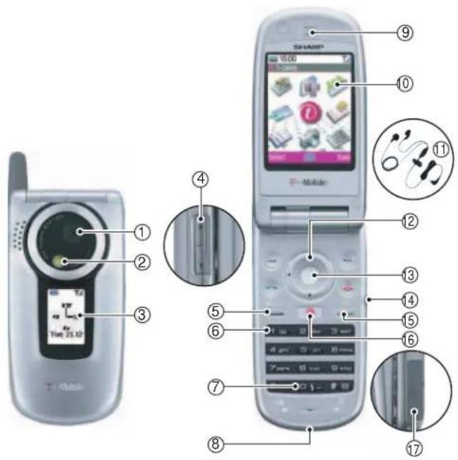
text_image
Diagram of a mobile phone with labeled parts including front panel, screen, and keypad, showing numbered annotations for each component.| No. | Name |
| 1 | 2-megapixel camera |
| 2 | LED flashlight |
| 3 | External display |
| 4 | Side-up/Side-down key |
| 5 | Camera/Music key |
| 6 | Voice mail key |
| 7 | Flashlight key |
| 8 | USB/charger connector |
| 9 | Earpiece |
| 10 | Main display |
| 11 | Handsfree earphones & microphone (stereo) |
| 12 | Navigation key (Up/Down/Left/Right)You can programme the Navigation Key yourself. |
| 13 | Centre key |
| 14 | Earphones connector |
| 15 | Font Zoom key |
| 16 | The t-zones Key also gives you direct access to the t-zones Online Homepage. |
| 17 | SD memory card slot |
3. OPERATION MANUAL
(Page numbers refer to the user guide)
[OPTIONAL ACCESSORIES]
- USB data cable The above accessories may not be available in all regions. For details, please contact your dealer.
CONFIDENTIAL
CHAPTER 2. 1 ADJUSTMENTS, PERFORMANCE CHECK, AND FIRMWARE UPGRADE
SPST (SHARP Program Support Tool) allows you to adjust settings, conduct performance checks, and upgrade the firmware.
[1] SHARP PROGRAM SUPPORT TOOL (SPST)
1. SYSTEM REQUIREMENTS
- IBM PC compatible personal computer (standard COM1 115,200 bps serial port and USB required)
Supported OS: Windows 98/98SE/2000/XP
(except for Windows 95/ME/NT)
(English, German, Italian, Spanish, French and Chinese versions) - Data cable
• GSM tester: CMU150
• GPIB interface: National Instruments USB-GPIB cable
(Model No.: NI GPIB-USB-B)
2. INTRODUCTION
2-1. FUNCTIONS
SPST offers seven key functions:
1) Firmware download
2) User data transfer (processes all data at once but not individually.)
3) RF calibration check and test
4) Default setting
5) Identification
6) Performance check and adjustment
7) User password reset
2-2. INSTALLATION
- Use Windows Explorer to execute the "setup.exe" file on the CD-ROM.
- The SPST TM200 setup wizard appears. Follow the installation instructions.
- After the installation is complete, shortcuts to SPST are created on the desktop and under the "Start"-Programs"-TM200" menu. Start SPST from the shortcuts.
2-3. STARTING UP
Connect TM200 to an operable serial port of the PC with the supplied data cable. Make sure that the battery is fully charged.
Start SPST from the desktop.
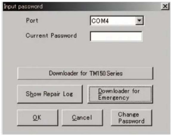
- The Input password dialog box appears. Enter the password, select a port where TM200 is connected from the list box, and click "OK". If you do not know SPC, click "Cancel" to exit.
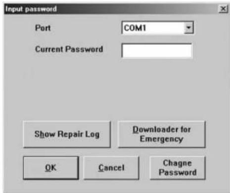
text_image
Input password Port COM1 Current Password Show Repair Log Downloader for Emergency OK Cancel Chagne Password- To change the password, enter the current password in procedure 1, and then click "Change Password".
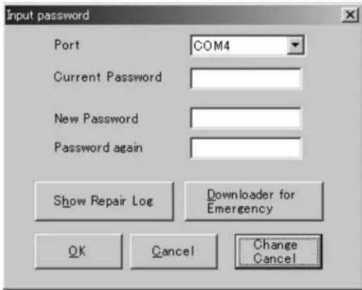
text_image
Input password Port COM4 Current Password New Password Password again Show Repair Log Downloader for Emergency OK Cancel Change Cancel- To check the usage status of tools, click "Show Repair Log" in procedure 1.
- Click "Downloader for Emergency".
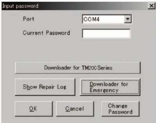
text_image
Input password Port COM4 Current Password Downloader for TM200 Series Show Repair Log Downloader for Emergency OK Cancel Change PasswordThe above screen appears. Select a model to use and execute the Downloader. (Use this to initialize the flash, etc.)
- When the password is correct, a connection is established and the following screen appears.

text_image
Refer to the attachment 1 for the destination and operator name. SPST for Vodafone Destination 1 T-Mobile Germany Products TM200 IMEI 83440000/49510000 Software ver. A02-006-0138-TM200 Default Set User Data Backup User Data Restore Downloader RE Calibration & Check RF Test User Password Reset Performance check adjustment **** mode release ExitCONFIDENTIAL
■ Buttons
| Default Set Refer to "4-1. Default setting". | |
| User Data Back-up Refer to "4-2. User data back-up". | |
| User Data Restore Refer to "4-3. User data restore". | |
| Downloader Refer to "4-4. Downloader". | |
| RF Calibration & Check | Refer to "4-5. RF calibration & check". |
| RF Test Refer to "4-6. RF test tool". | |
| User Password Reset Refer to "4-7. Password reset". | |
| Performance check adjustment | Refer to "4-8. Performance check and adjustment". |
| **** mode release Refer to "4-9. ****mode release". | |
| Exit End SPST. | |
3. ADJUSTMENTS FOR TM200
- Adjustments are required after replacing the following parts. ( ○ )
| Parts | Temperature adjustment (Camera) | Temperature adjustment (Battery) | Main display flicker adjustment | White defect correction |
| TH101 | × × | × | ||
| TH701 | × | × | × | |
| Main display unit | × | × | × | |
| Camera unit | × | × | × |
When replacing other parts in the RF section, carry out RF calibration.
- Click the buttons on the SPST screen for adjustments. 3. The following screen appears.
text_image
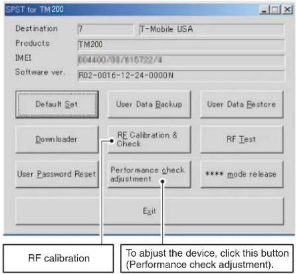
SPST for TM200 Destination 7 T-Mobile USA Products TM200 IMEI 004400/08/615722/4 Software ver. F02-0016-12-24-0000N Default Set User Data Backup User Data Restore Downloader RF Calibration & Check RF Test User Password Reset Performance check adjustment **** mode release Exit RF calibration To adjust the device, click this button (Performance check adjustment).
text_image
Performance check Main back light check External back light check Key back light check Memory check S-RAM PSRAM Check Sum LCD test Check White Orientation Red Green Blue Battery voltage check 60 read/write test Vibrator test Melody test Audio test Camera check PENDING Temperature adjustment (Canor section) Temperature adjustment (Battery section) Main display flicker adjustment External display contrast adjustment White defect correction Black defect correction Back to main menu① Temperature adjustment (Camera section)
② Temperature adjustment (Battery section)
③ Main display flicker adjustment
④ External display contrast adjustment
⑤ White defect correction
⑥ Black defect correction
CONFIDENTIAL
4. FUNCTIONS
4-1. DEFAULT SETTING
SPST can restore the factory settings.
This function
- Deletes all user data in the file system;
- Restores all WAP settings to default; and
- Restores the values set by the user to default;
(MEP_LOCK settings and the destination and operator name do not change.)
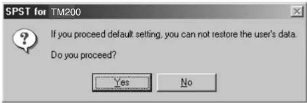
1) Set the COM port on the SPST initial screen and click "Default Set".
2) Click "Yes" to proceed. Click "No" to exit.
text_image
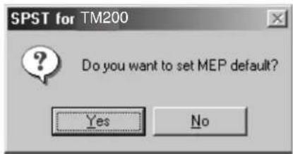
SPST for TM200 If you proceed default setting, you can not restore the user's data. Do you proceed? Yes No3) Click "Yes" to back-up the MEPLOCK data. Click "No" to restore default settings.
text_image
SPST for TM200 Do you want to set MEP default? Yes No4) Communication starts.

text_image
SPST communicating... Entering DIAG... Break5) The following appears when you select "Yes" in step 3 and MEPLOCK data exists. Click "Yes" to restore the data.

text_image
SPST for TM200 There is inputted data of MEPLOCK. Is this data restored? Yes No6) After the handset is turned on, the initialization is complete.
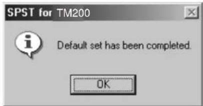
text_image
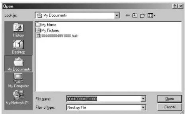
SPST for TM200 Default set has been completed. OK4-2. USER DATA BACK-UP
SPST saves all the data stored on the handset.
- Set the COM port on the SPST initial screen and click "User Data Back-up".
- Specify the file name in the following dialog box and click "Save"

text_image
Open Look in: My Documents My Music My Pictures bak History Desktop My Documents My Computer My Network FL... File name: 100.00000000 Files of type: Backup File Open Cancel- The communicating dialog box appears while processing.

text_image
SPST for TM200 User's data have been backed up completely. OK- When completed, the following message appears. Click "OK".

text_image
SPST communicating... Backup Library... Break4-3. USER DATA RESTORE
SPST completely restores the backed up data.
- Set the COM port on the SPST initial screen and click "User Data Restore".
- Specify the file name in the following dialog box and click "Save".
text_image
Open Look in: My Documents My Music My Pictures bak History Desktop My Documents My Computer My Network FL... File name: 1000000000 Files of type: Backup File Open CancelCONFIDENTIAL
- The communicating dialog box appears while processing.

text_image
Communicating... Restore Library... Break- When the restore is complete, click "OK".

text_image
SPST for TM200 User's data have been restored completely. OK4-4. DOWNLOADER
4-4-1. Introduction
Downloader allows you to upgrade the firmware.
1) System requirements
- Requirements for the upgrading tool:
OS : Windows 98, 98 SE, 2000, or XP
Download file : Only the Motorola format is supported.
Communication method : Asynchronous mode
Data length : 8 bits
Parity bit : None
Stop bit length : 1 bit
- Requirements for Loading loader
Handset : TM200
Communication method : Asynchronous mode
Data length : 8 bits
Parity bit : None
Stop bit length : 1 bit
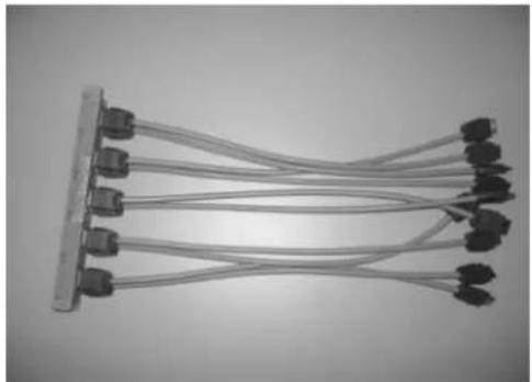
2) Required devices
The following devices are required to rewrite MOT files using Communication Box.
Conversion connector (16-pin → 10-pin)
This conversion connector is required to connect TM200 with Communication Box since the cable connector of Communication Box has 16 pins.
natural_image
Pure electrical circuit lines without any symbols4-4-2. Getting started
This section describes how to install/uninstall the software and how to connect handset to a PC.
1) Installing/uninstalling the software
[Installing the software]
Note: Downloader is installing/uninstalling simultaneously with SPTP.
- Double click the "setup.exe" icon in TM200 Install-E folder.
![SHARP TM200 - [Installing the software] - 1](/content/2026/06/1212016/images/0092873ca02857e0f161cfaf07030d6b6025b43046c8dadd1cbd6601e82b8d83.jpg)
setup.exe
- The Setup Wizard is activated.
Click the "Next" button.
![SHARP TM200 - [Installing the software] - 2](/content/2026/06/1212016/images/814bb5e3aeed0a485986bbbbefe2ed064dbda3b4fd8a5949c9fd9395e74e15a0.jpg)
text_image
The TM200 Upgrading Tool Welcome to the The TM200Upgrading Tool Setup Wizard The installer will guide you through the steps required to install TheTM200 Upgrading Tool on your computer. Click "Next" to continue. WARNING: This computer program is protected by copyright law and international treaties. Unauthorized duplication or distribution of this program, or any portion of it, may result in review civil or criminal penalties, and will be prosecuted to the authors extent possible under the law.- A location to install the software appears.
To install in the default location, click the "Next" button.
To change the location, click the "Browse" button, select a desired location and then click the "Next" button.
(See the description in "* Changing the install location" below.)
![SHARP TM200 - [Installing the software] - 3](/content/2026/06/1212016/images/f30742db6bbbf5795f3d5416a8f3361de09949f5deb05922498ba36dd111ba72.jpg)
text_image
The 19200 Upgrading Tool Select Installation Folder The install will install the tuzoolUpgrading Tool in the following folders. To install this folder, click "Next". To install to a different new or existing folder, enter one below or click "Browse". Folder: C:\Program Files\IThe19200UpgradingTool Browse... You can install the software on the following dsges: Volume Disk Size C: 4999M D: 2361 4 Disk Cost... Cancel Previous NextCONFIDENTIAL
\* Changing the install location
Click the "Browse" button in step 3 to browse folders.
Click the "▼" button, select a folder and click the "OK" button.

text_image
Browse for Folder Browse: The TM200 UpgradingTool Folder: C:\Program Files\The TM200 UpgradingTool\ OK Cancel4. A confirmation message appears.
Click the "Next" button.
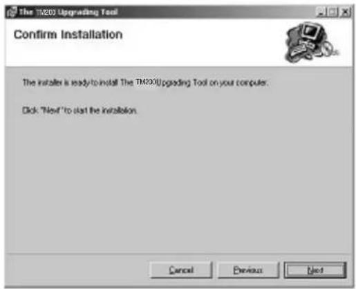
text_image
The TA200 Upgrading Tool Confirm Installation The installs is ready to install The TA200Upgrading Tool on your computer. Click "Next" to start the installation. Cancel Previous Next5. Installation starts. The progress is displayed.
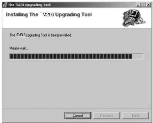
text_image
The TM200 Upgrading Tool Installing The TM200 Upgrading Tool The TM200 Upgrading Tool is being installed. Please wait... Cancel Cancel Next6. The installation is completed.
Click the "Close" button to close the Setup Wizard.
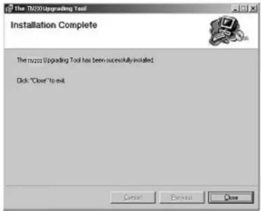
text_image
The TM200 Upgrading Tool Installation Complete TheTM200 Upgrading Tool has been successfully installed Click "Close" to exit Cancel Exhibit Close7. The shortcut icon shown left is created on your desktop when the installation is completed.

Note:
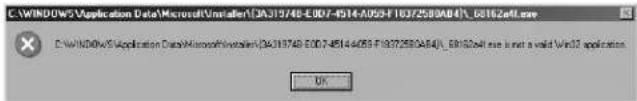
• After installing the upgrading tool in Windows 98 or 98 SE, restart the operating system.
While installing the upgrading tool in Windows 98, 98 SE, or ME, a message may appear prompting to restart the operating system. In this case, restart your operating system following the instruction. Even if the message does not appear, restart your operating system after the installation.
On Windows 98, if you start the upgrading tool without restarting the operation system, the following message may appear. Restart the operating system to ensure the proper operation of the upgrading tool.
text_image
C:\WINDOWSApplication Data\Microsoft\Installer\34313748-007-4514-A059-F16372589A84\34313748-007-4514-A059-F16372589A84\34313748-007-4514-A059-F16372589A84\34313748-007-4514-A059-F16372589B4\34313748-007-4514-A059-F16372589A84\34313748-007-4514-A059-F16372589A84\34313748-007-4514-A059-F1637258A84\34313748-007-4514-A059-F16372589A84\34313748-007-4514-A059-F16372589A84\34313748-007-4514-A059-F1637260A84\34313748-007-4514-A059-F1637260A84\34313748-007-4514-A059-F1637260A84\34313748-007-4514-A059-F1637260B4\34313748-007-4514-A059-F1637260A84\34313748-007-4514-A059-F1637260A84\34313748-007-4514-A059-F1637260A8- Uninstall the upgrading tool before installing the latest version or reinstalling the current version.
Otherwise, the upgrading tool may not function properly.
To ensure the proper operation, uninstall and then reinstall the upgrading tool.
CONFIDENTIAL
[Uninstalling the software]
- Double click "setup.exe" in TM200 Install-E folder.
![SHARP TM200 - [Uninstalling the software] - 1](/content/2026/06/1212016/images/d425f1e2d0fda7bed1aec625aff121bcda397e36c571004f5581db46c34ddc61.jpg)
setup.exe
- The Setup Wizard is activated. Select "Remove The TM200 Upgrading Tool" and click the "Finish" button.
![SHARP TM200 - [Uninstalling the software] - 2](/content/2026/06/1212016/images/5f1ddd19d3b3488b1d3e34ef5749f48af86cce31bca13be1c8d22586995e4898.jpg)
text_image
The TM200 Upgrading Tool Welcome to the The TM200 Upgrading Tool Setup Wizard Select whether you want to repair or remove The TM200Upgrading Tool Repair The TM200 Upgrading Tool Reserve The TM200Upgrading Tool WARNING: This computer program is protected by copyright law and international treaties. Unauthorized duplication or distribution of this program, or any portion of it, may result in universal civil or criminal penalties, and will be prosecuted to the maximum extent possible under the law. Cancel Finish Finish- Uninstallation starts. The progress is displayed.
![SHARP TM200 - [Uninstalling the software] - 3](/content/2026/06/1212016/images/dad2c5adf08049e9b83a0e36470e466a271560760fbdc629b13e86e43dc43f1b.jpg)
text_image
The TM200 Upgrading Tool Removing The TM200 Upgrading T... TheTM200 Upgrading Tool is being removed. Please wait... Cancel Cancel Next- The uninstallation is completed. Click the "Close" button to close the Setup Wizard.
![SHARP TM200 - [Uninstalling the software] - 4](/content/2026/06/1212016/images/9ac71f92dd92764dc3730667ad6cb0c4b410d9789852d59d8855bb470dafd9c8.jpg)
text_image
The TW200 Upgrading Tool Installation Complete The TW200 Upgrading Tool has been successfully removed. Click "Close" to exit.2) Connecting handset to a PC
A) Using a cable for upgrading
- Connect the cable to a PC.
- Connect the cable to handset.
- The photo below shows handset connected to a PC.

natural_image
Black-and-white photo of a laptop connected to a flexible mobile phone and cable (no visible text or symbols)B) Using Communication Box
- Connect a PC to Communication Box via a serial cable.
- Connect the AC charger to Communication Box and then plug it into the outlet.
All SET POWER SW on Communication Box must be turned off.
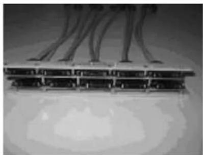
- Connect the conversion connector to Communication Box Cables. Connect the conversion connector in the following order, label side up. From upper right end: Cable No. 1, 3, 5, 7, and 9. From lower right end: Cable No. 2, 4, 6, 8, and 10.
natural_image
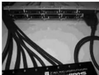
Close-up of a multi-pin electronic device with visible leads (no text or symbols)- The photo below shows the conversion connector connected to Communication Box Cable 1.
natural_image
Close-up of black cables bundled between two network equipment units (no visible text or symbols)CONFIDENTIAL
- Connect the other end of the conversion connector to handset.
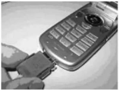
natural_image
Close-up of a hand inserting a USB into a mobile phone (no visible text or symbols)- The photo below shows handset, Communication Box and a PC (all connected). Make sure handset and Communication Box Cable 1 are connected via the conversion connector.
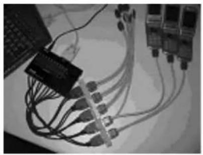
natural_image
Close-up of electronic circuit boards connected to a central module (no visible text or symbols)Note:
- Handset must be turned off before making any connections. Press and hold the Power key to turn off handset. Do not turn off in other ways. Malfunction may occur and the MOT file rewrite operation may fail.
- Make sure the handset battery is sufficiently charged. If the battery is low, the MOT file rewrite operation may fail. Charge the battery before the operation.
- Disconnect the AC charger from a cable for upgrading. When rewriting MOT files using the upgrading tool, do not connect the AC charger to the cable. If you connect the cable connected to the AC charger to handset, charging starts and the MOT file rewrite operation is interrupted.
- All SET POWER SW on Communication Box must be turned off. If handset is connected with SET POWER SW turned on, charging starts and the MOT file rewrite operation is interrupted.
- Make sure handset and Communication Box Cable 1 are connected via the conversion connector. (When using Communication Box, the only handset connected to Cable 1 can be operated on the PC.)
4-4-3. Rewriting MOT files
This section describes how to rewrite MOT files.
1) Downloader for Emergency
- Click "Downloader for Emergency".
text_image
Input password Port COM4 Current Password Downloader for TM150 Series Show Repair Log Downloader for Emergency OK Cancel Change Password- The upgrading tool is activated.
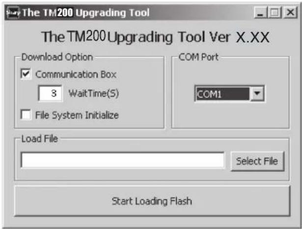
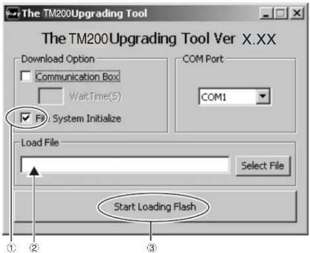
text_image
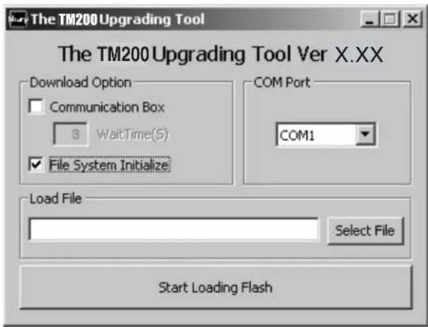
The TM200 Upgrading Tool The TM200Upgrading Tool Ver X.XX Download Option ✓ Communication Box 3 WaitTime(S) ☐ File System Initialize COM Port COM1 Load File Select File Start Loading FlashNote: Disable the power saving mode before rewriting MOT files. If the power saving mode is active, the rewrite operation may fail depending on the PC.
CONFIDENTIAL
2) Selecting options and COM port
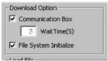
① Uncheck the check box when using a cable for upgrading. Leave it checked when using Communication Box.
② To initialize user area, check the File System Initialize check box. (User data will be deleted and the handset status will return to the default.)
③ Click here and in the pull-down list, select a communications port where the cable or Communication Box is connected.

text_image
The TM200 Upgrading Tool Ver X.XX Download Option Communication Box 3 WaitTime(5) COM Port COM1 COM1 COM2 COM3 COM4 COM5 COM6 COM7 COM8 COM9 Load File File Start Loading FlashWhen using Communication Box, set Wait Time.
Check the Communication Box check box to adjust Wait Time (default: 3 seconds). The time to delete the program data varies between handsets. Handsets wait for the set Wait Time until the whole process is completed. If an error occurs, increase the value.
text_image
Download Option ✓ Communication Box 3 Wait Time(S) ✓ File System Initialize[Notes for the Wait Time setting]
When the set value is smaller than the default (3), the message on the left appears alerting you a possible error.
Click the [OK] button to proceed, and click the [Cancel] button to change the value.
![SHARP TM200 - [Notes for the Wait Time setting] - 1](/content/2026/06/1212016/images/a830950671079d541a499fd6f25378d88baf0faa660685c7de67ce16db137f4d.jpg)
text_image
Information Since Wait Time is set up lower than a default, a error may occur. Is processing started ? OK CancelYou can shorten time for the MOT rewrite operation by selecting a smaller value for Wait Time.
Example: Time to rewrite two MOT files at a time.
At the default setting (3 seconds), rewrite time is approximately 40 minutes. If the value is set to 1, the rewrite time will be reduced to approximately 30 minutes.
If an error occurs at 1, increase the value.
The error screen will appear on handsets No. 2 to No.10.
If this screen appears, increase Wait Time and retry.
![SHARP TM200 - [Notes for the Wait Time setting] - 2](/content/2026/06/1212016/images/8676f9057153301fe6337ea2475990e43ef00fe9c69fbbfb05de50328d1d3e2b.jpg)
text_image
Error screen Flash Loader 5.02 CORRESPONDENCE_ERRORWhen the File System Initialize check box is checked, a confirmation message appears.
![SHARP TM200 - [Notes for the Wait Time setting] - 3](/content/2026/06/1212016/images/178ef62b9bb07c93b123620583129d0573ae51641bbd5bee5052064cbe13c818.jpg)
text_image
Information User Data will be erased during Initialization. Are you sure you want to initialize the File System ? OK Cancel Click the [OK] button.Note: When you check File System Initialize check box and click the [OK] button, handset status returns to the default. In this case, user data is initialized after the MOT file rewrite operation. Uncheck the check box to avoid this.
3) Selecting a MOT file
- Click the [Select File] button.
The Open dialog box appears.
text_image
The TM200 Upgrading Tool The TM200 Upgrading Tool Ver X.XX Download Option Communication Box 8 WaitTime(S) File System Initialize COM Port COM1 Load File Select File Start Loading FlashCONFIDENTIAL
[Open dialog box]
① Click the [▼] button to open a desired folder.
② A Motorola file (.mot) in the folder appears. Click a file to write in.
③ Click the [Open] button to open the file.
![SHARP TM200 - [Open dialog box] - 1](/content/2026/06/1212016/images/4abcc0369afd085dbc830d1cf90f9096b547e0578f8b99c576052a44028bba80.jpg)
text_image
Open Look in: MOT-File 1500-25 478.mot File name: >150-25-25.mot Files of type: Motorola Files (*.mot) Open CancelNote:
• Make sure to select a MOT file.
If the File name field is blank, you cannot rewrite a MOT file.
- Use MOT files in the hard disk.
If the selected MOT file is stored in other locations, an error message appears and you cannot complete the rewrite operation.

text_image
Error Unable to Open file OKTo use MOT files on CDs or on the network, copy or download them to the hard disk first.
4) Rewriting a MOT file
Click the [Start Loading Flash] button to start rewriting.

text_image
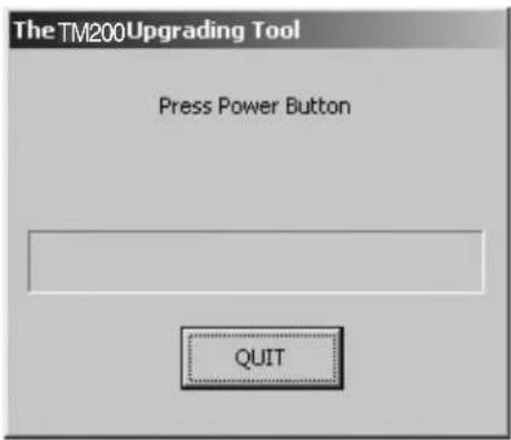
The TM200 Upgrading Tool The TM200 Upgrading Tool Ver X.XX Download Option Communication Box 3 WaitTime(S) File System Initialize COM Port COM1 Load File C:\Documents and Settings\Administrator\Desktop Select File Start Loading Flash- "Press Power Button" appears.
Hold down the Power key.
Turn on Communication Box SW from No.10 down to No.1 (turn on only the handsets you are using).
text_image
The TM200Upgrading Tool Press Power Button QUIT- "Keep Pressing Power Button" appears.
Hold down the Power key until the "Keep Pressing Power Button" disappears.
Leave the Communication Box SW turned on.

text_image
The TM200Upgrading Tool Sync received ; Sending File to RAM ... Keep Pressing Power Button QUIT- The MOT file rewrite operation starts.
When "Keep Pressing Power Button" disappears, release the Power key.
Leave the Communication Box SW turned on.
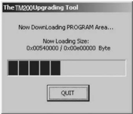
text_image
The TM200Upgrading Tool Now Downloading PROGRAM Area... Now Loading Size: 0x00540000 / 0x00e00000 Byte QUITCONFIDENTIAL
- When the rewrite operation starts, handset display screen shows the software version and process of communications with the PC.
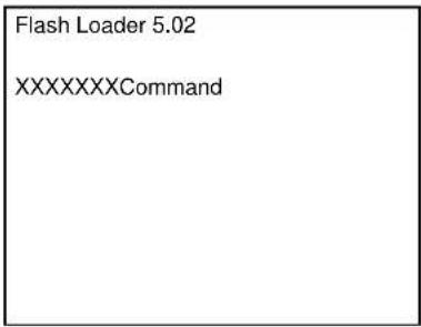
text_image
Flash Loader 5.02 XXXXXXXXCommandCanceling the ongoing rewrite operation:
Click the [QUIT] button.
To rewrite MOT files later, remove and install the battery first.
[Notes for the use of a cable for upgrading]
- Disconnect the AC charger from the cable. Otherwise charging starts and the MOT file rewrite operation is interrupted.
- Make sure the handset battery is sufficiently charged. If the battery is low, the rewrite operation may fail. Charge the battery before the operation.
- If the ongoing rewrite operation is canceled, or interrupted by an error, remove and reinstall the battery and retry.
[Notes for the use of the Communication Box]
- When "Press Power Button!" appears, turn on Communication Box SW from No.10 down to No.1. If the communication BoxSW No.1 is first turned on, the rewrite on communication BoxSW No. 2 to No. 10 operation will fail.
- The time to delete the program data varies between handsets. If the process fails at the default Wait Time (3 seconds), increase the value. Consequently, this will increase the time to complete the rewrite operation.
5) Checking the value of SUM
When the rewrite operation is completed, a confirmation message appears with SUM.

text_image
Information Now Process Complete!! SUM = 0xdb3d OKSUM also appears on handset.
After 8 seconds, SUM disappears.
When SET POWER SW is turned off, SUM disappears.
Flash Loader 5.02
SUM Check End
SUM = 0xdb3d
Make sure SUM is the same between the PC and handset.
The same SUM means that the rewrite operation is completed properly. If the value is different, try again to ensure completion of the operation.
If the MOT file rewrite operation fails, an error message appears on handset.
* The screen shot on the left shows an error in erasing Flash data. [ADR] and [STR] appear only when an error occurs in the FLASH-related operation.
Start over the MOT file rewrite operation.
Find the message in 4-4-4. 2) Error messages for Loading loader, and follow the instructions.
Error screen
| Flash Loader 5.02 |
| FLASH_ERROR |
| ERROR_ERASE |
| ADR = 0x1000000 |
| STR = 0xA0 |
6) After the operation
Disconnect the cable for upgrading from handset. When using the Communication Box, turn off SET POWER SW and then disconnect the cable from handset.
CONFIDENTIAL
7) Initializing only the file system
Follow the instructions below to initialize only the file system. (User data will be deleted and the handset status will return to the default.)
* Perform this procedure when the handset does not turn on.
① Check the File System Initialize check box.
② Leave the Load File text box blank.
③ Click the [Start Loading Flash] button.
text_image
The TM200Upgrading Tool Ver X.XX Download Option Communication Box WaitTime(S) ✓ File System Initialize COM Port COM1 Load File Select File Start Loading FlashFor further operations, refer to [4-4-3. 4) Rewriting a MOT file] or [4-4-3. 5) Checking the value of SUM].
4-4-4. Error message list
Below is the list of error messages for the upgrading tool (on the PC side) and Loading loader (on the handset side).
1) Error messages for the upgrading tool (on the PC side)
| No. | Message Descriptions/Instructions | |
| 1 | Select a file for Downloading or check the box of Initializing. | Load File is not set. Select a MOT file. |
| 2 | Unable to open file. Failed to open the MOT file.Start over the rewrite operation. | |
| 3 | You need to set the Wait Time! WaitTime (S) is not set.Set WaitTime (S) value. | |
| 4 | The file you selected is unsuitable for Upgrading. | The selected file cannot be rewritten for upgrading.Select an appropriate MOT file. |
| 5 | Cannot Setup COM port. The selected COM port does not exist or is used for other operations.Select a COM port connected to the PC cable. | |
| 6 | RAM Loader not responding to Commands. | No response from Loading loader.Start over the rewrite operation. |
| 7 | RAM Loader responding Parameter Error. | Information sent from the PC is illegal.Reinstall the upgrading tool. Start over the rewrite operation. |
| 8 | RAM Loader responding Flash Error (XXXX). | Failed to initialize FLASH ROM in (XXXX).Start over the rewrite operation. |
| 9 | Correspondence Error. Undefined response from Loading loader.Start over the rewrite operation. | |
2) Error messages for Loading loader (on the handset side)
| No. | Message Descriptions/Instructions | |
| 1 | FLASH_ERROR An error in Flash Rom.Start over the rewrite operation. | |
| 2 | ERROR_PARAM The upgrading tool is damaged.Uninstall and reinstall the upgrading tool,and start over the rewrite operation. | |
| 3 | ERROR_WPROTECT Flash Rom is protected.Battery may be too low.Use a sufficiently charged battery andstart over the rewrite operation. | |
| 4 | ERROR_READ Failed to read Flash Rom data and theoperation was aborted.Start over the rewrite operation. | |
| 5 | ERROR_WRITE Failed to write to Flash Rom and theoperation was aborted.Start over the rewrite operation. | |
| 6 | ERROR_ERASE Failed to erase Flash Rom data and theoperation was aborted.Start over the rewrite operation. | |
| 7 | ERROR_VERIFY The rewrite operation was aborted sincethere was a mismatch between data writ-ten to Flash Rom and that written tohandset.Start over the rewrite operation. | |
| 8 | ERROR_RWE_TMOUT Communication was terminated sincethere was no response from Flash Romfor a certain period of time.Start over the rewrite operation. | |
| 9 | CORRESPONDENCE_ERROR Communication was terminated sinceserial data communication failed.Start over the rewrite operation. | |
| 10 | ADR = XXXXXXXX Indicates the address of Flash(the error source). | |
| 11 | STR = XX Indicates the status of Flash(the error source). | |
* When No.1 occurs, handset screen shows error messages for No.2 to No.8 as well as the address (No.10) and status (No.11) of the error source at the same time.
4-5. RF CALIBRATION & CHECK

flowchart
graph TD
    A["Stabilized power supply"] --> B["Handset"]
    B --> C["RF cable"]
    B --> D["GSM tester"]
    D --> E["GPIB cable"]
    E --> F["PC"]
    G["Test battery"] --> B
    H["Data cable"] --> F
4-5-1. Preparation
- Connect PC and GSM tester with a GPIB cable.
- Connect PC and handset with a Data cable. (Use a test battery or one close.)
- Connect a RF cable of GSM tester to handset.
CONFIDENTIAL
4-5-2. Default setting for the program.
- Activate the program and set defaults.
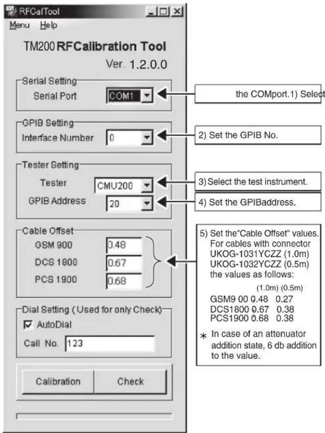
text_image
RFCaTool Menu Help TM200 RFCalibration Tool Ver. 1.2.0.0 Serial Setting Serial Port COM1 GPIB Setting Interface Number 0 Tester Setting Tester CMU200 GPIB Address 20 Cable Offset GSM 900 0.48 DCS 1800 0.67 PCS 1900 0.68 Dial Setting (Used for only Check) AutoDial Call No. 123 Calibration Check the COMport.1) Select 2) Set the GPIB No. 3) Select the test instrument. 4) Set the GPIBaddress. 5) Set the"Cable Offset" values. For cables with connector UKOG-1031YCZZ (1.0m) UKOG-1032YCZZ (0.5m) the values as follows: (1.0m) (0.5m) GSM9 00 0.48 0.27 DCS1800 0.67 0.38 PCS1900 0.68 0.38 * In case of an attenuator addition state, 6 db addition to the value.- Make sure the handset is on and click "OK". (Adjustment starts.)
text_image
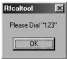
Rfcaltool Please Dial "123" OK- Click "OK".
text_image
Rfcaltool RF Calibration completed. OK- The initial screen returns.
4-5-4. RF performance check (Insert SIM card)
- Apply 4 V using a stabilized power supply and turn on the handset.
- Start "RF calibration & check" on SPST and click "Calibration".
- When initialization is complete, click "OK".

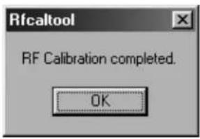
4-5-3. RF calibration (Remove SIM card)
- Apply 4 V using a stabilized power supply and turn on the handset.
- Start "RF calibration & check" on SPST and click "Calibration".
- When initialization is complete, click "OK".

- Apply 4 V using a stabilized power supply and turn on the handset. After the handset enters Standby mode, lower the voltage to 3.7 V.
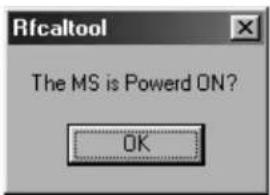
text_image
Rfcaltool The MS is Powered ON? OK- Apply 4 V using a stabilized power supply and turn on the handset. After the handset enters Standby mode, lower the voltage to 3.7 V.
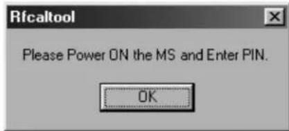
text_image
Rfcaltool Please Power ON the MS and Enter PIN. OK- Make sure the handset is in the idle mode and click "OK".
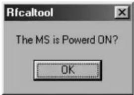
text_image
Rfcaltool The MS is Powered ON? OKCONFIDENTIAL
- Press the keys 1, 2, 3 and Send and click "OK".

text_image
Rfcaltool Please Dial "123" OK- Make sure the terminal display is "In Call" and click "OK". (RF performance check starts.)

text_image
Rfcaltool The Call was Established? OK- The following message appears during the check. Press the keys 1, 2, 3 and Send again and click "OK".

text_image
Rfcaltool Please Dial "123" OK- Make sure the terminal display is "In Call" and click "OK".

text_image
Rifcaltool The Call was Established? OK- RF performance check is complete. Click "Save As..." and name the file to save the result. Click "OK" to exit.
text_image
Results Lots of Results ALL NG No Value Item CH PO 1 31.375 OK 2 31.674 OK 3 31.444 OK 4 20.897 OK 5 4.910E OK 6 -3.549 E OK 7 1.200 E OK 8 3.359E OK 9 1.266E OK 10 1.2717 OK 11 1.3264 OK 12 4.270E OK 13 4.537E OK 14 5.2201 OK 15 -72.33 E OK 16 -70.94 E OK 17 65.821 OK Total: 342 NG: 0 OK Save As... OKThe following will be displayed in case of failure. See the attachment 2 for troubleshooting.

text_image
Result -Us of Results ALL NG No Value Item CH PCL 1 31.572 OK 116 27.674-Bust Power 512 0 2 31.856 OK 229 28.037-Bust Power 661 0 3 31.276 OK 230 27.692-Bust Power 512 0 4 31.114 OK 342 33 RV Level Reports 661 0 5 5.7331 OK 6 -0.059 OK 7 -1.029 OK 8 3.580 OK 9 1.3042 OK 10 1.2781 OK 11 1.3376 OK 12 4.4895 OK 13 4.5882 OK 14 5.0552 OK 15 -72.01 OK 16 -71.04 OK 17 -66.13 OK Total: 342 NG: 4 NG Save As... OK- Click "OK".

text_image
Rfcaltool RF Check Completed. OK- The initial screen returns.
CONFIDENTIAL
Attachment 2
Whole inspection list by RF performance check.
| Band | Sending/Receive | No. | Item to be inspected | Channel | PCL |
| GSM900 | Tx 1 Burst | Power | 37CH PCL5 | ||
| 2 Burst Power | 975CH PCL5 | ||||
| 3 Burst Power | 124CH PCL5 | ||||
| 4 Burst Power | 37CH PCL11 | ||||
| 5 Burst Power | 37CH PCL19 | ||||
| 6 Frequency Error | 37CH PCL5 | ||||
| 7 Frequency Error | 975CH PCL5 | ||||
| 8 Frequency Error | 124CH PCL5 | ||||
| 9 Phase Error (RMS) | 37CH PCL5 | ||||
| 10 Phase Error (RMS) | 975CH PCL5 | ||||
| 11 Phase Error (RMS) | 124CH PCL5 | ||||
| 12 Phase Error (Peak) | 37CH PCL5 | ||||
| 13 Phase Error (Peak) | 975CH PCL5 | ||||
| 14 Phase Error (Peak) | 124CH PCL5 | ||||
| 15 Mod_spectrum | -800 | 37CH PCL5 | |||
| 16 Mod_spectrum | -600 | 37CH PCL5 | |||
| 17 Mod_spectrum | -400 | 37CH PCL5 | |||
| 18 Mod_spectrum | -250 | 37CH PCL5 | |||
| 19 Mod_spectrum | -200 | 37CH PCL5 | |||
| 20 Mod_spectrum | +200 | 37CH PCL5 | |||
| 21 Mod_spectrum | +250 | 37CH PCL5 | |||
| 22 Mod_spectrum | +400 | 37CH PCL5 | |||
| 23 Mod_spectrum | +600 | 37CH PCL5 | |||
| 24 Mod_spectrum | +800 | 37CH PCL5 | |||
| 25 Mod_spectrum | -800 | 975CH PCL5 | |||
| 26 Mod_spectrum | -600 | 975CH PCL5 | |||
| 27 Mod_spectrum | -400 | 975CH PCL5 | |||
| 28 Mod_spectrum | -250 | 975CH PCL5 | |||
| 29 Mod_spectrum | -200 | 975CH PCL5 | |||
| 30 Mod_spectrum | +200 | 975CH PCL5 | |||
| 31 Mod_spectrum | +250 | 975CH PCL5 | |||
| 32 Mod_spectrum | +400 | 975CH PCL5 | |||
| 33 Mod_spectrum | +600 | 975CH PCL5 | |||
| 34 Mod_spectrum | +800 | 975CH PCL5 | |||
| 35 Mod_spectrum | -800 | 124CH PCL5 | |||
| 36 Mod_spectrum | -600 | 124CH PCL5 | |||
| 37 Mod_spectrum | -400 | 124CH PCL5 | |||
| 38 Mod_spectrum | -250 | 124CH PCL5 | |||
| 39 Mod_spectrum | -200 | 124CH PCL5 | |||
| 40 Mod_spectrum | +200 | 124CH PCL5 | |||
| 41 Mod_spectrum | +250 | 124CH PCL5 | |||
| 42 Mod_spectrum | +400 | 124CH PCL5 | |||
| 43 Mod_spectrum | +600 | 124CH PCL5 | |||
| 44 Mod_spectrum | +800 | 124CH PCL5 | |||
| 45 Mod_spectrum | -800 | 37CH PCL11 | |||
| 46 Mod_spectrum | -600 | 37CH PCL11 | |||
| 47 Mod_spectrum | -400 | 37CH PCL11 | |||
| Band | Sending/Receive | No. | Item to be inspected | Channel | PCL |
| GSM900 | Tx | 48 Mod_spectrum -250 | 37CH PCL1 | 1 | |
| 49 Mod_spectrum -200 | 37CH PCL1 | 1 | |||
| 50 Mod_spectrum +200 | 37CH PCL1 | 1 | |||
| 51 Mod_spectrum +250 | 37CH PCL1 | 1 | |||
| 52 Mod_spectrum +400 | 37CH PCL1 | 1 | |||
| 53 Mod_spectrum +600 | 37CH PCL1 | 1 | |||
| 54 Mod_spectrum +800 | 37CH PCL1 | 1 | |||
| 55 Mod_spectrum -800 | 37CH PCL1 | 9 | |||
| 56 Mod_spectrum -600 | 37CH PCL1 | 9 | |||
| 57 Mod_spectrum -400 | 37CH PCL1 | 9 | |||
| 58 Mod_spectrum -250 | 37CH PCL1 | 9 | |||
| 59 Mod_spectrum -200 | 37CH PCL1 | 9 | |||
| 60 Mod_spectrum +200 | 37CH PCL1 | 9 | |||
| 61 Mod_spectrum +250 | 37CH PCL1 | 9 | |||
| 62 Mod_spectrum +400 | 37CH PCL1 | 9 | |||
| 63 Mod_spectrum +600 | 37CH PCL1 | 9 | |||
| 64 Mod_spectrum +800 | 37CH PCL1 | 9 | |||
| 65 Switch_Spectrum -1800 | 37CH PCL5 | 5 | |||
| 66 Switch_Spectrum -1200 | 37CH PCL5 | 5 | |||
| 67 Switch_Spectrum -600 | 37CH PCL5 | 5 | |||
| 68 Switch_Spectrum -400 | 37CH PCL5 | 5 | |||
| 69 Switch_Spectrum +400 | 37CH PCL5 | 5 | |||
| 70 Switch_Spectrum +600 | 37CH PCL5 | 5 | |||
| 71 Switch_Spectrum +1200 | 37CH PCL5 | 5 | |||
| 72 Switch_Spectrum +1800 | 37CH PCL5 | 5 | |||
| 73 Switch_Spectrum -1800 | 975CH PCL5 | 5 | |||
| 74 Switch_Spectrum -1200 | 975CH PCL5 | 5 | |||
| 75 Switch_Spectrum -600 | 975CH PCL5 | 5 | |||
| 76 Switch_Spectrum -400 | 975CH PCL5 | 5 | |||
| 77 Switch_Spectrum +400 | 975CH PCL5 | 5 | |||
| 78 Switch_Spectrum +600 | 975CH PCL5 | 5 | |||
| 79 Switch_Spectrum +1200 | 975CH PCL5 | 5 | |||
| 80 Switch_Spectrum +1800 | 975CH PCL5 | 5 | |||
| 81 Switch_Spectrum -1800 | 124CH PCL5 | 5 | |||
| 82 Switch_Spectrum -1200 | 124CH PCL5 | 5 | |||
| 83 Switch_Spectrum -600 | 124CH PCL5 | 5 | |||
| 84 Switch_Spectrum -400 | 124CH PCL5 | 5 | |||
| 85 Switch_Spectrum +400 | 124CH PCL5 | 5 | |||
| 86 Switch_Spectrum +600 | 124CH PCL5 | 5 | |||
| 87 Switch_Spectrum +1200 | 124CH PCL5 | 5 | |||
| 88 Switch_Spectrum +1800 | 124CH PCL5 | 5 | |||
| 89 Switch_Spectrum -1800 | 37CH PCL11 | 1 | |||
| 90 Switch_Spectrum -1200 | 37CH PCL11 | 1 | |||
| 91 Switch_Spectrum -600 | 37CH PCL11 | 1 | |||
| 92 Switch_Spectrum -400 | 37CH PCL11 | 1 | |||
CONFIDENTIAL
| Band | Sending/Receive | No. | Item to be inspected | Channel | PCL |
| GSM900 | Tx 93 Switch | Spectrum +400 37CH PCL11 | |||
| 94 Switch_Spectrum +600 37CH PCL11 | |||||
| 95 Switch_Spectrum +1200 37CH PCL11 | |||||
| 96 Switch_Spectrum +1800 37CH PCL11 | |||||
| 97 Switch_Spectrum -1800 37CH PCL19 | |||||
| 98 Switch_Spectrum -1200 37CH PCL19 | |||||
| 99 Switch_Spectrum -600 37CH PCL19 | |||||
| 100 Switch_Spectrum -400 37CH PCL19 | |||||
| 101 Switch_Spectrum +400 37CH PCL19 | |||||
| 102 Switch_Spectrum +600 37CH PCL19 | |||||
| 103 Switch_Spectrum +1200 37CH PCL19 | |||||
| 104 Switch_Spectrum +1800 37CH PCL19 | |||||
| 105 Burst Timing 37CH PCL5 | |||||
| 106 Burst Timing 975CH PCL5 | |||||
| 107 Burst Timing 124CH PCL5 | |||||
| 108 Burst Timing 37CH PCL11 | |||||
| 109 Burst Timing 37CH PCL19 | |||||
| Rx 110 Rx | Sensitivity 37CH PCL5 | ||||
| 111 Rx Sensitivity | 975CH PCL5 | ||||
| 112 Rx Sensitivity | 124CH PCL5 | ||||
| 113 Usable Receiver Level 37CH PCL5 | |||||
| 114 Rx Level Reports | 37CH PCL5 | ||||
| DCS | Tx | 115 Burst Power | 699CH PCL0 | ||
| 116 Burst Power | 512CH PCL0 | ||||
| 117 Burst Power | 855CH PCL0 | ||||
| 118 Burst Power | 699CH PCL5 | ||||
| 119 Burst Power | 699CH | PCL15 | |||
| 120 Frequency Error | 699CH PCL0 | ||||
| 121 Frequency Error | 512CH PCL0 | ||||
| 122 Frequency Error | 885CH PCL0 | ||||
| 123 Phase Error (RMS) | 699CH PCL0 | ||||
| 124 Phase Error (RMS) | 512CH PCL0 | ||||
| 125 Phase Error (RMS) | 885CH PCL0 | ||||
| 126 Phase Error (Peak) | 699CH PCL0 | ||||
| 127 Phase Error (Peak) | 512CH PCL0 | ||||
| 128 Phase Error (Peak) | 855CH PCL0 | ||||
| 129 Mod_spectrum -800 | 699CH PCL0 | ||||
| 130 Mod_spectrum -600 | 699CH PCL0 | ||||
| 131 Mod_spectrum -400 | 699CH PCL0 | ||||
| 132 Mod_spectrum -250 | 699CH PCL0 | ||||
| 133 Mod_spectrum -200 | 699CH PCL0 | ||||
| 134 Mod_spectrum +200 | 699CH PCL0 | ||||
| 135 Mod_spectrum +250 | 699CH PCL0 | ||||
| 136 Mod_spectrum +400 | 699CH PCL0 | ||||
| 137 Mod_spectrum +600 | 699CH PCL0 | ||||
| 138 Mod_spectrum +800 | 699CH PCL0 | ||||
| 139 Mod_spectrum -800 | 512CH PCL0 | ||||
| Band | Sending/Receive | No. | Item to be inspected | Channel | PCL |
| DCS Tx | 140 | Mod_spectrum -600 | 512CH PCL0 | ||
| 141 Mod_spectrum -400 | 512CH PCL0 | ||||
| 142 Mod_spectrum -250 | 512CH PCL0 | ||||
| 143 Mod_spectrum -200 | 512CH PCL0 | ||||
| 144 Mod_spectrum +200 | 512CH PCL0 | ||||
| 145 Mod_spectrum +250 | 512CH PCL0 | ||||
| 146 Mod_spectrum +400 | 512CH PCL0 | ||||
| 147 Mod_spectrum +600 | 512CH PCL0 | ||||
| 148 Mod_spectrum +800 | 512CH PCL0 | ||||
| 149 Mod_spectrum -800 | 885CH PCL0 | ||||
| 150 Mod_spectrum -600 | 885CH PCL0 | ||||
| 151 Mod_spectrum -400 | 885CH PCL0 | ||||
| 152 Mod_spectrum -250 | 885CH PCL0 | ||||
| 153 Mod_spectrum -200 | 885CH PCL0 | ||||
| 154 Mod_spectrum +200 | 885CH PCL0 | ||||
| 155 Mod_spectrum +250 | 885CH PCL0 | ||||
| 156 Mod_spectrum +400 | 885CH PCL0 | ||||
| 157 Mod_spectrum +600 | 885CH PCL0 | ||||
| 158 Mod_spectrum +800 | 885CH PCL0 | ||||
| 159 Mod_spectrum -800 | 699CH PCL5 | ||||
| 160 Mod_spectrum -600 | 699CH PCL5 | ||||
| 161 Mod_spectrum -400 | 699CH PCL5 | ||||
| 162 Mod_spectrum -250 | 699CH PCL5 | ||||
| 163 Mod_spectrum -200 | 699CH PCL5 | ||||
| 164 Mod_spectrum +200 | 699CH PCL5 | ||||
| 165 Mod_spectrum +250 | 699CH PCL5 | ||||
| 166 Mod_spectrum +400 | 699CH PCL5 | ||||
| 167 Mod_spectrum +600 | 699CH PCL5 | ||||
| 168 Mod_spectrum +800 | 699CH PCL5 | ||||
| 169 Mod_spectrum -800 | 699CH | PCL15 | |||
| 170 Mod_spectrum -600 | 699CH | PCL15 | |||
| 171 Mod_spectrum -400 | 699CH | PCL15 | |||
| 172 Mod_spectrum -250 | 699CH | PCL15 | |||
| 173 Mod_spectrum -200 | 699CH | PCL15 | |||
| 174 Mod_spectrum +200 | 699CH | PCL15 | |||
| 175 Mod_spectrum +250 | 699CH | PCL15 | |||
| 176 Mod_spectrum +400 | 699CH | PCL15 | |||
| 177 Mod_spectrum +600 | 699CH | PCL15 | |||
| 178 Mod_spectrum +800 | 699CH | PCL15 | |||
| 179 Switch_Spectrum -1800 | 699CH PCL0 | ||||
| 180 Switch_Spectrum -1200 | 699CH PCL0 | ||||
| 181 Switch_Spectrum -600 | 699CH PCL0 | ||||
| 182 Switch_Spectrum -400 | 699CH PCL0 | ||||
| 183 Switch_Spectrum +400 699CH PCL0 | |||||
| 184 Switch_Spectrum +600 699CH PCL0 | |||||
| 185 Switch_Spectrum +1200 | 699CH PCL0 | ||||
| 186 Switch_Spectrum +1800 | 699CH PCL0 | ||||
| 187 Switch_Spectrum -1800 | 512CH PCL0 | ||||
CONFIDENTIAL
| Band | Sending/Receive | No. | Item to be inspected | Channel | PCL |
| DCS Tx 1 | 88 Switch | Spectrum -1200 512CH PCL0 | |||
| 189 | Switch_Spectrum -600 512 | CH PCL0 | |||
| 190 | Switch_Spectrum -400 512 | CH PCL0 | |||
| 191 | Switch_Spectrum +400 512 | CH PCL0 | |||
| 192 | Switch_Spectrum +600 512 | CH PCL0 | |||
| 193 | Switch_Spectrum +1200 512 | CH PCL0 | |||
| 194 | Switch_Spectrum +1800 512 | CH PCL0 | |||
| 195 | Switch_Spectrum -1800 885 | CH PCL0 | |||
| 196 | Switch_Spectrum -1200 885 | CH PCL0 | |||
| 197 | Switch_Spectrum -600 885 | CH PCL0 | |||
| 198 | Switch_Spectrum -400 885 | CH PCL0 | |||
| 199 | Switch_Spectrum +400 885 | CH PCL0 | |||
| 200 | Switch_Spectrum +600 885 | CH PCL0 | |||
| 201 | Switch_Spectrum +1200 885 | CH PCL0 | |||
| 202 | Switch_Spectrum +1800 885 | CH PCL0 | |||
| 203 | Switch_Spectrum -1800 699 | CH PCL5 | |||
| 204 | Switch_Spectrum -1200 699 | CH PCL5 | |||
| 205 | Switch_Spectrum -600 699 | CH PCL5 | |||
| 206 | Switch_Spectrum -400 699 | CH PCL5 | |||
| 207 | Switch_Spectrum +400 699 | CH PCL5 | |||
| 208 | Switch_Spectrum +600 699 | CH PCL5 | |||
| 209 | Switch_Spectrum +1200 699 | CH PCL5 | |||
| 210 | Switch_Spectrum +1800 699 | CH PCL5 | |||
| 211 | Switch_Spectrum -1800 699 | CH PCL15 | |||
| 212 | Switch_Spectrum -1200 699 | CH PCL15 | |||
| 213 | Switch_Spectrum -600 699 | CH PCL15 | |||
| 214 | Switch_Spectrum -400 699 | CH PCL15 | |||
| 215 | Switch_Spectrum +400 699 | CH PCL15 | |||
| 216 | Switch_Spectrum +600 699 | CH PCL15 | |||
| 217 | Switch_Spectrum +1200 699 | CH PCL15 | |||
| 218 | Switch_Spectrum +1800 699 | CH PCL15 | |||
| 219 | Burst Timing 699CH PCL0 | ||||
| 220 | Burst Timing 512CH PCL0 | ||||
| 221 | Burst Timing 885CH PCL0 | ||||
| 222 | Burst Timing 699CH PCL5 | ||||
| 223 | Burst Timing 699CH PCL15 | ||||
| Rx 224 Rx | Sensitivity 699CH PCL0 | ||||
| 225 | Rx Sensitivity 512CH PCL0 | ||||
| 226 | Rx Sensitivity 885CH PCL0 | ||||
| 227 | Usable Receiver Level 699 | CH PCL0 | |||
| 228 | Rx Level Reports 699CH PCL0 | ||||
| PCS Tx 2 | 29 Burst Power | 661CH PCL0 | |||
| 230 | Burst Power | 512CH PCL0 | |||
| 231 | Burst Power | 810CH PCL0 | |||
| Band | Sending/Receive | No. | Item to be inspected | Channel | PCL |
| PCS Tx 23 | 32 Burst P | Power | 661CH PCL5 | ||
| 233 | Burst Power | 661CH PCL15 | |||
| 234 | Frequency Error | 661CH PCL0 | |||
| 235 | Frequency Error | 512CH PCL0 | |||
| 236 | Frequency Error | 810CH PCL0 | |||
| 237 | Phase Error (RMS) | 661CH PCL0 | |||
| 238 | Phase Error (RMS) | 512CH PCL0 | |||
| 239 | Phase Error (RMS) | 810CH PCL0 | |||
| 240 | Phase Error (Peak) | 661CH PCL0 | |||
| 241 | Phase Error (Peak) | 512CH PCL0 | |||
| 242 | Phase Error (Peak) | 810CH PCL0 | |||
| 243 | Mod_spectrum -800 | 661CH PCL0 | |||
| 244 | Mod_spectrum -600 | 661CH PCL0 | |||
| 245 | Mod_spectrum -400 | 661CH PCL0 | |||
| 246 | Mod_spectrum -250 | 661CH PCL0 | |||
| 247 | Mod_spectrum -200 | 661CH PCL0 | |||
| 248 | Mod_spectrum +200 | 661CH PCL0 | |||
| 249 | Mod_spectrum +250 | 661CH PCL0 | |||
| 250 | Mod_spectrum +400 | 661CH PCL0 | |||
| 251 | Mod_spectrum +600 | 661CH PCL0 | |||
| 252 | Mod_spectrum +800 | 661CH PCL0 | |||
| 253 | Mod_spectrum -800 | 512CH PCL0 | |||
| 254 | Mod_spectrum -600 | 512CH PCL0 | |||
| 255 | Mod_spectrum -400 | 512CH PCL0 | |||
| 256 | Mod_spectrum -250 | 512CH PCL0 | |||
| 257 | Mod_spectrum -200 | 512CH PCL0 | |||
| 258 | Mod_spectrum +200 | 512CH PCL0 | |||
| 259 | Mod_spectrum +250 | 512CH PCL0 | |||
| 260 | Mod_spectrum +400 | 512CH PCL0 | |||
| 261 | Mod_spectrum +600 | 512CH PCL0 | |||
| 262 | Mod_spectrum +800 | 512CH PCL0 | |||
| 263 | Mod_spectrum -800 | 810CH PCL0 | |||
| 264 | Mod_spectrum -600 | 810CH PCL0 | |||
| 265 | Mod_spectrum -400 | 810CH PCL0 | |||
| 266 | Mod_spectrum -250 | 810CH PCL0 | |||
| 267 | Mod_spectrum -200 | 810CH PCL0 | |||
| 268 | Mod_spectrum +200 | 810CH PCL0 | |||
| 269 | Mod_spectrum +250 | 810CH PCL0 | |||
| 270 | Mod_spectrum +400 | 810CH PCL0 | |||
| 271 | Mod_spectrum +600 | 810CH PCL0 | |||
| 272 | Mod_spectrum +800 | 810CH PCL0 | |||
| 273 | Mod_spectrum -800 | 661CH PCL5 | |||
| 274 | Mod_spectrum -600 | 661CH PCL5 | |||
| 275 | Mod_spectrum -400 | 661CH PCL5 | |||
| 276 | Mod_spectrum -250 | 661CH PCL5 | |||
| 277 | Mod_spectrum -200 | 661CH PCL5 | |||
| 278 | Mod_spectrum +200 | 661CH PCL5 | |||
| 279 | Mod_spectrum +250 | 661CH PCL5 | |||
| 280 | Mod_spectrum +400 | 661CH PCL5 | |||
CONFIDENTIAL
| Band | Sending/Receive | No. | Item to be inspected | Channel | PCL |
| PCS Tx 281 Mod_spectrum +600 661CH PCL5 | |||||
| 282 Mod_spectrum +800 661CH PCL5 | |||||
| 283 Mod_spectrum -800 661CH PCL15 | |||||
| 284 Mod_spectrum -600 661CH PCL15 | |||||
| 285 Mod_spectrum -400 661CH PCL15 | |||||
| 286 Mod_spectrum -250 661CH PCL15 | |||||
| 287 Mod_spectrum -200 661CH PCL15 | |||||
| 288 Mod_spectrum +200 661CH PCL15 | |||||
| 289 Mod_spectrum +250 661CH PCL15 | |||||
| 290 Mod_spectrum +400 661CH PCL15 | |||||
| 291 Mod_spectrum +600 661CH PCL15 | |||||
| 292 Mod_spectrum +800 661CH PCL15 | |||||
| 293 Switch_Spectrum -1800 661CH PCL0 | |||||
| 294 Switch_Spectrum -1200 661CH PCL0 | |||||
| 295 Switch_Spectrum -600 661CH PCL0 | |||||
| 296 Switch_Spectrum -400 661CH PCL0 | |||||
| 297 Switch_Spectrum +400 661CH PCL0 | |||||
| 298 Switch_Spectrum +600 661CH PCL0 | |||||
| 299 Switch_Spectrum +1200 661CH PCL0 | |||||
| 300 Switch_Spectrum +1800 661CH PCL0 | |||||
| 301 Switch_Spectrum -1800 512CH PCL0 | |||||
| 302 Switch_Spectrum -1200 512CH PCL0 | |||||
| 303 Switch_Spectrum -600 512CH PCL0 | |||||
| 304 Switch_Spectrum -400 512CH PCL0 | |||||
| 305 Switch_Spectrum +400 512CH PCL0 | |||||
| 306 Switch_Spectrum +600 512CH PCL0 | |||||
| 307 Switch_Spectrum +1200 512CH PCL0 | |||||
| 308 Switch_Spectrum +1800 512CH PCL0 | |||||
| 309 Switch_Spectrum -1800 810CH PCL0 | |||||
| 310 Switch_Spectrum -1200 810CH PCL0 | |||||
| 311 Switch_Spectrum -600 810CH PCL0 | |||||
| 312 Switch_Spectrum -400 810CH PCL0 | |||||
| 313 Switch_Spectrum +400 810CH PCL0 | |||||
| 314 Switch_Spectrum +600 810CH PCL0 | |||||
| 315 Switch_Spectrum +1200 810CH PCL0 | |||||
| 316 Switch_Spectrum +1800 810CH PCL0 | |||||
| 317 Switch_Spectrum -1800 661CH PCL5 | |||||
| 318 Switch_Spectrum -1200 661CH PCL5 | |||||
| 319 Switch_Spectrum -600 661CH PCL5 | |||||
| 320 Switch_Spectrum -400 661CH PCL5 | |||||
| 321 Switch_Spectrum +400 661CH PCL5 | |||||
| 322 Switch_Spectrum +600 661CH PCL5 | |||||
| 323 Switch_Spectrum +1200 661CH PCL5 | |||||
| 324 Switch_Spectrum +1800 661CH PCL5 | |||||
| Band | Sending/Receive | No. | Item to be inspected | Channel | PCL |
| PCS Tx 325 Switch_ | Spectrum -1800 661CH PCL15 | ||||
| 326 | Switch_Spectrum -1200 | 661CH PCL15 | |||
| 327 | Switch_Spectrum -600 | 661CH PCL15 | |||
| 328 | Switch_Spectrum -400 | 661CH PCL15 | |||
| 329 | Switch_Spectrum +400 | 661CH PCL15 | |||
| 330 | Switch_Spectrum +600 | 661CH PCL15 | |||
| 331 | Switch_Spectrum +1200 | 661CH PCL15 | |||
| 332 | Switch_Spectrum +1800 | 661CH PCL15 | |||
| 333 | Burst Timing | 661CH PCL0 | |||
| 334 | Burst Timing | 512CH PCL0 | |||
| 335 | Burst Timing | 810CH PCL0 | |||
| 336 | Burst Timing | 661CH PCL5 | |||
| 337 | Burst Timing | 661CH PCL15 | |||
| Rx | 338 | Rx Sensitivity | 661CH PCL0 | ||
| 339 | Rx Sensitivity | 512CH PCL0 | |||
| 340 | Rx Sensitivity | 810CH PCL0 | |||
| 341 | Usable Receiver Level 661CH PCL0 | ||||
| 342 | Rx Level Reports | 661CH PCL0 | |||
■ Troubleshooting list
| Test items | Check parts for GSM900 | Check parts for DCS | Check parts for PCS |
| Tx | |||
| Burst Power | IC802, IC803, FL905 | IC802, IC803, FL905 | IC802, IC803, FL905 |
| Frequency Error | TCX801 | TCX801 | TCX801 |
| Phase Error | IC801 | IC801 | IC801 |
| Mod_spectrum | IC801, TCX801 | IC801, TCX801 | IC801, TCX801 |
| Switch_Spectrum | IC801, IC802 IC803 | IC801, IC802 IC803 | IC801, IC802, IC803 |
| Burst Timing | IC802 | IC802 | IC802 |
| Rx | |||
| Rx Sensitivity | IC801, IC803, FL902, FL905 | IC801, IC803, FL902, FL905 | IC801, IC803, FL903, FL905 |
| Usable Receiver Level | IC801 | IC801 | IC801 |
| Rx Level Reports | IC801, IC803, FL902, FL905 | IC801, IC803, FL902, FL905 | IC801, IC803, FL903, FL905 |
4-6. RF TEST TOOL
4-6-1. Requirements
For repairs, this test checks the condition of an electric board (especially the RF section).
- PC with COM port
• TM200 Data Cable - PWB repair jig
• GSM Tester (CMU200)
CONFIDENTIAL
4-6-2. Setup
- Set PWB and make connections as shown below. Make sure connections are correct at the points shown below.

text_image
Hook PWB Hook Hook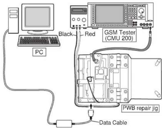
text_image
PC Black Red GSM Tester (CMU 200) PWB repair jig Data Cable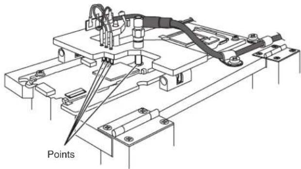
text_image
Points- Apply 4 V using a stabilized power supply and turn on the handset.
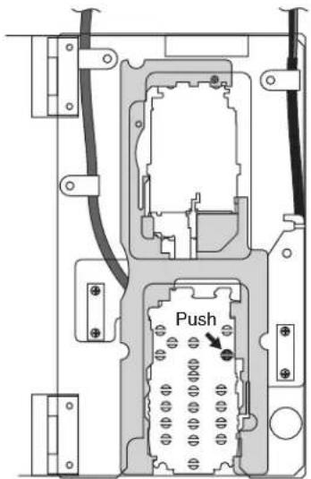
text_image
Push- Start RF test tool.
- Select a COM port to which Data Cable is connected.
- Press the "Initialize & Read Data" button.

text_image
COM Port COM1 Initialize & Read Data- The figure shown below appears (wait a few seconds).
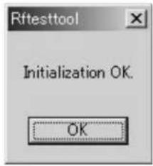
text_image
Rftesttool Initialization OK. OK- Click "OK" to proceed.
4-6-3. Tests
1) BAND Select & Channel
Select a band and a channel to test. Settings are applied to all tests.

text_image
BAND Select GSM(900) Channel 975 124 975 Band selection Channel bar Input box[Procedure]
- Select a band. (GSM900, DCS or PCS)
- Select or enter a channel using Channel bar or Input box.
CONFIDENTIAL
2) TX test
Test burst transmission.

text_image
TX frequency of selected channels Current PCL (Read only) TX Test 880.2 [MHz] PCL Setting 5 19 PCL 5 TX ON Data Pattern All 0 All 1 1010 0101 TSC 5 This indicator appears during burst transmission. Data patterns PCL bar TX ON/OFF button ( | )[Procedure]
- Select a band and channel. [See 4-6-13. 1)]
- Select PCL (Power Control Level) using PCL bar.
- Select Data pattern.
- Click TX ON to start burst transmission. (You can check each part in this state.)
- Click TX OFF to end burst transmission.
* Data pattern (TSC 5) includes Training Sequence GSM 5, and other part is pseudo random data.
TM200 TX power Table (25°C, voltage: 3.7[V])
■ GSM900 Band ■ DCS/PCS Band
| PCL | GSM900 | Tolerance |
| [dBm] | ||
| 5 | 3 | 3 - 2 dB |
| 6 | 3 | 1 - 3 dB |
| 7 | 2 | 9 - 3 dB |
| 8 | 2 | 7 - 3 dB |
| 9 | 2 | 5 - 3 dB |
| 10 23 | +/ | - 3 dB |
| 11 21 | +/ | - 3 dB |
| 12 19 | +/ | - 3 dB |
| 13 17 | +/ | - 3 dB |
| 14 15 | +/ | - 3 dB |
| 15 13 | +/ | - 3 dB |
| 16 11 | +/ | - 5 dB |
| 17 9 | +/ | - 5 dB |
| 18 7 | +/ | - 5 dB |
| 19 5 | +/ | - 5 dB |
| PCL | DCS/PCS | Tolerance |
| [dBm] | ||
| 0 | 3 | 0 |
| 1 | 2 | 8 |
| 2 | 2 | 6 |
| 3 | 2 | 4 |
| 4 | 2 | 2 |
| 5 | 2 | 0 |
| 6 | 1 | 8 |
| 7 | 1 | 6 |
| 8 | 1 | 4 |
| 9 | 1 | 2 |
| 10 10 | +/- 4 dB | |
| 11 8 | +/- 4 dB | |
| 12 6 | +/- 4 dB | |
| 13 4 | +/- 4 dB | |
| 14 2 | +/- 5 dB | |
| 15 0 | +/- 5 dB |
3) RX test
The handset receives burst signals in this test.

text_image
RX Test 925.2 [MHz] RX Gain Setting[dB] -6 94 Gain -6 [dB] RX ON Burst Receive with Sniff SniffOFF This indicator appears while receiving burst signals. Sniff ON/OFF ) | ( ) RX ON/OFF button RX frequency of selected channels Current RX Gain (Read only)TM200 1ADJUSTMENTS, PERFORMANCE CHECK, AND FIRMWARE UPGRADE
CONFIDENTIAL
[Procedure]
- Select a channel and band. [see 4-6-3.1)]
- Select RX Gain using RX Gain Setting bar.
- Choose Sniff ON or OFF.
- Click "RX ON" to start receiving burst signals.
- From GSM tester, send burst signals in the specified channel. (You can check each part in this state.)
- Click "RX OFF" to end receiving burst signals.
*In this test, the reception timing cannot be synchronized with burst signals from Signal Generator or GSM tester.
*The standard RX Gain Setting is: (Input power at the aerial connector of the handset) + (RX Gain) = -16 dBm Excessive Input power or RX Gain may cause damage to the handset.
4) RSSI Measure
The handset notifies you of input power value at the aerial connector.

text_image
RSSI Measure Estimated Power(Integer) [dBm] Measure Measured Power [dBm] Estimated Power Input box (Integeronly) Measure button Measured power box[Procedure]
- Connect the handset and GSM tester (or Signal Generator) with RF cable.
- Select a band and channel. [see 4-6-3.1)]
- Send signals ( *) from GSM tester.
- Enter the value of input power from GSM tester in integers (from -10 to -110) considering RF cable loss.
- Press the [Measure] button.
- The result appears in Measured Power box.
*The signal type from GSM tester must be either of two:
- Continuous sine wave (without modulation) with the frequency as follows:
(Frequency of the measured channel) + 67.708kHz.
(Ex. channel: GSM 37ch → the result: 942.467708 MHz)
Power: -110 to -10 dBm
- BCCH signal of the measured channel Power: -110 to -10 dBm
Result
When the handset is properly calibrated, the error between "Estimated Power" and "Measured Power" is less than 3dB.
4-6-4. Termination
Turn off the handset to ensure proper operations.
4-6-5. Trouble information
When switching DCS and PCS, change the channel number as well. Or the band does not change properly.
Example: If you change DCS 512 CH to PCS 512 CH, the band remains DCS.
4-7. Password reset
SPST resets the password (handset code is set to "0000").
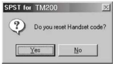
1) Set the COM port on the SPST initial screen and click "User Password Reset". Click "Yes" to reset. Click "No" to exit.
text_image
SPST for TM200 Do you reset Handset code? Yes No2) When completed, the following appears.

text_image
SPST for TM200 User password reset has been completed. OK4-8. Performance check and adjustment
With this function, SPST checks the performance of the handset and makes adjustments.
1) Set the COM port on the SPST initial screen and click "Performance check and adjustment". The following dialog box appears while processing.

text_image
SPST communicating... Entering DIAG... Break2) When completed, the following is displayed. Click "Back to main menu" to exit.
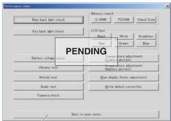
text_image
Performance check Memory check S-RAM PSRAM Check Sum Main back light check Key back light check LCD test Black White Gradation Red Green Blue Battery voltage check Vibrator test Temperature adjustment (Camera section) Temperature adjustment (Battery section) Melody test Main display flicker adjustment Audio test White defect correction Camera check Back to main menu PENDINGThe functions of each button are described below.
CONFIDENTIAL
4-8-1. Main back light check
The main display backlight turns on and the message appears on the PC.
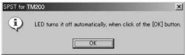
text_image
SPST for TM200 LED turns it off automatically, when click of the [OK] button. OKCheck the backlight and press "OK".
- If a failure occurs, see "10. Back Light does not turn on." in [3] Troubleshooting.
4-8-2. External back light check
The external display back light turns on and the message appears on the PC. Check the back light and press "OK".
- If a failure occurs, see "10. Back Light does not turn on." in [3] Troubleshooting.
4-8-3. Key back light check
The keypad back light turns on and the message appears on the PC. Check the back light and press "OK".
4-8-4. LED check
The LED lights up in a specified color and the message appears on the PC. Check the LED and press "OK".
- If a failure occurs, see "15. Flash light does not work." in [3] Troubleshooting.
4-8-5. Battery voltage check
Click to display the current battery voltage.
- If a failure occurs, see "1. Power is not turned on." in [3] Troubleshooting.
4-8-6. SD read/write test
Insert an SD card (otherwise a message prompts you to do so and click the button to perform the SD card read/write test.
- If a failure occurs, see "17. SD (Memory) card is not recognized." in [3] Troubleshooting.
4-8-7. Vibrator test
Click to vibrate the handset. Click "OK" to exit.
- If a failure occurs, see "5. Vibrator does not work." in [3] Troubleshooting.
4-8-8. Melody test
A message describes test items. Click "Yes" to proceed and "No" to exit.
The order of the test items:
speaker → hands free → hands free (stereo) → speaker (analog melody)

flowchart
graph LR
    A["Trouble found by SPST"] --> B["(1) Speaker"]
    A --> C["(2) Hands free Sound is heard in audio test."]
    A --> D["(3) Hands free (stereo)"]
    A --> E["(4) Speaker (analog melody)"]
    B --> F["→"]
    C --> G["→"]
    D --> H["→"]
    E --> I["→"]
    F --> J["See "Speaker does not work.""]
    G --> K["Parts between IC105 pin 10 and IC103 pin 93 are defective, or IC103 is defective."]
    H --> L["See "Hands free kit (monaural headset)" in the section *3. No voice is heard from the earpiece."]
    I --> M["Parts between IC105 pin 10 and IC103 pin 93; IC105 pin 11 and IC103 pin 94 are defective. Otherwise IC103 is defective."]
    J --> N["See "Hands free kit (stereo headset) - Option *in the section "No voice is heard from the earpiece.""]
    K --> O["See "Video/Voice Recorder playback is impossible.""]
    L --> P["Otherwise parts between IC105 pin 10 and IC103 pin 93 are defective, or IC103 is defective."]
4-8-9. Audio test
The following appears.
text_image
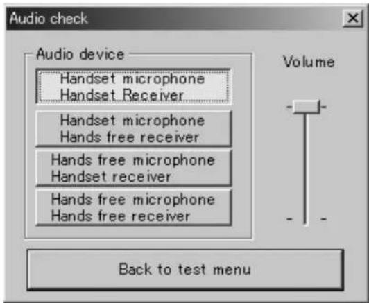
Audio check Audio device Handset microphone Handset Receiver Handset microphone Hands free receiver Hands free microphone Handset receiver Hands free microphone Hands free receiver Volume Back to test menuSelect a test item from Audio device. Check the output sound from the receiver by speaking to the microphone, etc. Click "Back to test menu" to return to the previous screen.
CONFIDENTIAL

flowchart
graph TD
    A["Trouble found by SPST"] --> B["(1) Handset microphone\nHandset receiver"]
    A --> C["(2) Handset microphone\nHands free receiver"]
    A --> D["(3) Hands free microphone\nHands free receiver"]
    A --> E["(4) Hands free microphone\nHandset receiver"]
    B --> F["(1) & (2): No voice is heard."]
    C --> G["(1) & (2): No voice is heard."]
    D --> H["(3)&(4): No voice is heard."]
    E --> I["(3) & (4): No voice is heard."]
    F --> J["(1) & (2): No voice is heard."]
    G --> K["(1) & (2): No voice is heard."]
    H --> L["(3) & (4): No voice is heard."]
    I --> M["(3) & (4): No voice is heard."]
    J --> N["(1) & (2): No voice is heard."]
    K --> O["(1) & (2): No voice is heard."]
    L --> P["(1) & (2): No voice is heard."]
    M --> Q["(1) & (2): No voice is heard."]
    N --> R["(1) & (2): No voice is heard."]
    O --> S["(1) & (2): No voice is heard."]
    P --> T["(1) & (2): No voice is heard."]
    Q --> U["(1) & (2): No voice is heard."]
    R --> V["(1) & (2): No voice is heard."]
    S --> W["(1) & (2): No voice is heard."]
    T --> X["(1) & (2): No voice is heard."]
    U --> Y["(1) & (2): No voice is heard."]
    V --> Z["(1) & (2): No voice is heard."]
    W --> AA["(1) & (2): No voice is heard."]
    X --> AB["(1) & (2): No voice is heard."]
    Y --> AC["(1) & (2): No voice is heard."]
    Z --> AD["(1) & (2): No voice is heard."]
    AA --> AE["(1) & (2): No voice is heard."]
    AB --> AF["(1) & (2): No voice is heard."]
    AC --> AG["(1) & (2): No voice is heard."]
    AD --> AH["(1) & (2): No voice is heard."]
    AE --> AI["(1) & (2): No voice is heard."]
    AF --> AJ["(1) & (2): No voice is heard."]
    AG --> AK["(1) & (2): No voice is heard."]
    AH --> AL["(1) & (2): No voice is heard."]
    AI --> AM["(1) & (2): No voice is heard."]
    AJ --> AN["(1) & (2): No voice is heard."]
    AK --> AO["(1) & (2): No voice is heard."]
    AL --> AP["(1) & (2): No voice is heard."]
    AM --> AQ["(1) & (2): No voice is heard."]
    AN --> AR["(1) & (2): No voice is heard."]
    AO --> AS["(1) & (2): No voice is heard."]
    AP --> AT["(1) & (2): No voice is heard."]
    AQ --> AU["(1) & (2): No voice is heard."]
    AR --> AV["(1) & (2): No voice is heard."]
4-8-10. Camera check
The following appears.
text_image
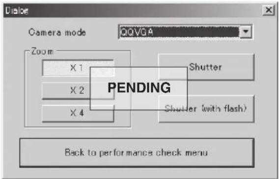
Dialog Camera mode OOVA Zoom X 1 X 2 X 4 PENDING Shutter Shutter (with flash) Back to performance check menuSelect a Camera mode from the pull-down menu. Click "Shutter" to check that the camera operates properly. Click "Back to performance check menu" to return to the previous screen.
- If a failure occurs, see "10. Pictures cannot be taken." in [3] Troubleshooting.
4-8-11. Memory check
Click "S-RAM" and "PSRAM" to see each test result.
For "Check Sum", the calculation appears after the SPST communicating dialog box.
4-8-12. LCD test
Check that the specified color appears on the main display.
- If a failure occurs, see "12. The display does not appear on Main Display." and "13. The display does not appear on External Display (in 65K color mode)." in [3] Troubleshooting.
4-8-13. Temperature adjustment
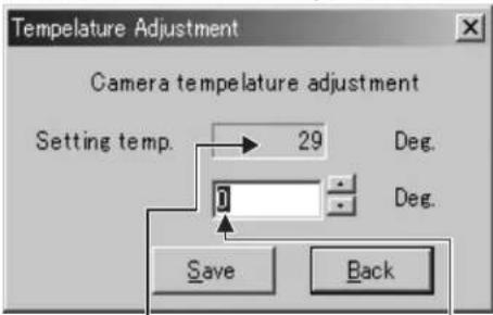
The following appears.
Setting temp. indicates the current temperature. The relative temperature is displayed in the text box below.
(Only the relative temperature is adjustable.)
If displayed Setting temp. value differs from the current temperature, click [▲] or [▼] to set a correction value in the range of -99 to +99 and click "Save"
text_image
Tempelature Adjustment Camera tempelature adjustment Setting temp. 29 Deg. 0 Deg. Save BackCorrection value = (Setting temp.) - (current temp.) + (displayed correction value)
4-8-14. Main display flicker adjustment
The following is displayed.
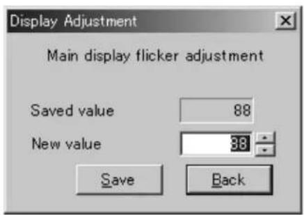
text_image
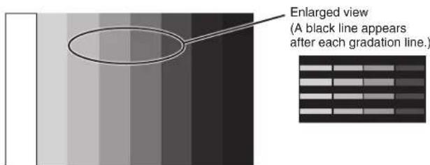
Display Adjustment Main display flicker adjustment Saved value 88 New value 88 Save BackCheck a main display visually within a distance of 20 cm from a fluorescent light, and adjust the value to minimize flicker on the display with the ▲ and [▼] buttons. Click "Save" and confirm that the main display does not flicker. (Fine adjustment for DC voltage between display electrodes)
text_image
Enlarged view (A black line appears after each gradation line.)8-level graduation pattern with alternate black and gradation lines (black and white)
4-8-15. External display contrast adjustment
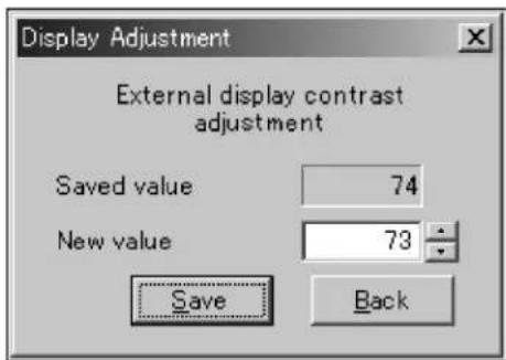
Click the "External display contrast adjustment" button. The following screen appears.
text_image
Display Adjustment External display contrast adjustment Saved value 74 New value 73 Save BackCONFIDENTIAL

bar_stacked
| Category | Value | |---|---| | Dark Grey | 10 | | Medium Grey | 8 | | Light Grey | 6 | | Pale Grey | 4 | | White | 2 | | Light Grey | 1 | | White | 0 | DEN: 0758-level gradation pattern (black & white pattern)
Comparing with an adjusted handset, click "▲" or "▼" to adjust the value so that the same gradation pattern is displayed. Click "Save" and confirm the pattern on the external display.
4-8-16. White defect correction
* White defect correction:
Defective pixels in a camera light sensor appear as bright points in the display even when light is blocked completely (display is all black). Perform white defect correction to eliminate errors in these pixels.
- Protect the handset camera from light completely with a black cover.
- Click the "White defect correction" button. The following screen appears.

text_image
SPST for ITM200 Please cover the lens of a camera.(hands, black thing, etc...) Is it ready? Yes NoClick the "Yes" button and leave it for about 20 seconds. When completed, the following message appears.

text_image
SPST for TM200 White defect correction is completed. OKWhen an error occurs, the corresponding message appears. Solve the problem according to "Solution".
- Error 1
Error message: "There are too many white cracks."
Cause : The light is not sufficiently blocked.
Solution :Block the light completely and perform white defect correction again.
- Error 2
Error message : "There are many white cracks."
Cause : The light is not sufficiently blocked.
Solution :Block the light completely and perform white defect correction again.
- Error 3
Error message : "There are too many white cracks cannot be rectified."
Cause :There is a hardware error.
Solution :Replace the camera unit.
4-8-17. Black defect correction
* Black defect correction:
Defective pixels in a camera light sensor appear as black points in the display even when a captured image is completely white (display is all white). Perform black defect correction to eliminate errors in these pixels.
1) Requirements
• Desk top type of fluorescent lamp
- Black defect correction sheet
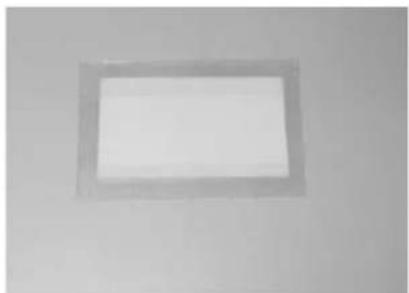
natural_image
Blank rectangular frame with no visible text, symbols, or markings- Illuminance meter
2) Procedure
- Cover the camera section with the black defect correction sheet as shown in Figure 96.
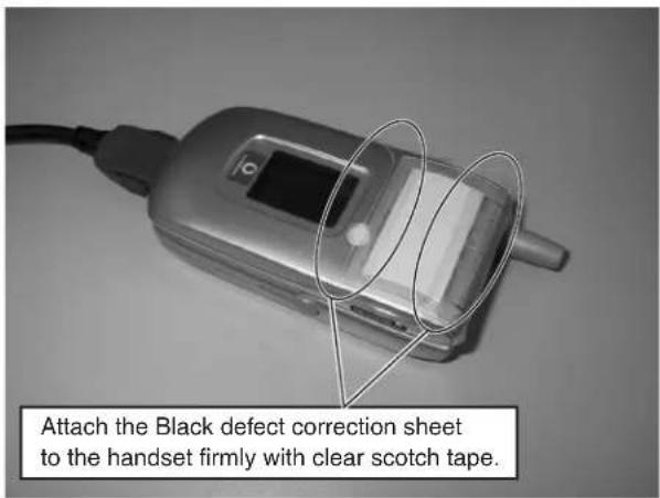
text_image
Attach the Black defect correction sheet to the handset firmly with clear scotch tape.- Check the distance from the fluorescent lamp by using an illuminance meter. In the proper position for black defect correction, illuminance is between 8,000 and 10,000 lux.

natural_image
Person using a handheld electronic device on a workbench with electronic components and a portable radio nearby (no visible text or symbols)CONFIDENTIAL
- Hold the handset in the proper position.
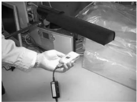
natural_image
Person in lab coat holding a small electronic device, with a handheld device and plastic bag in background (no visible text or symbols)- Click the "Black defect correction" button.
The following message is displayed.

text_image
SPST Please take a some white things with camera. Is it ready? Yes No- Click the "Yes" button. Communication starts.

text_image
SPST communicating... Correcting black defect... Break- The result is displayed within a minute as follows.
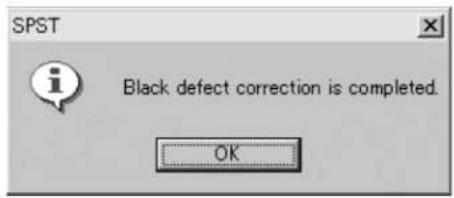
text_image
SPST Black defect correction is completed. OKWhen an error occurs, the corresponding message appears. Solve the problem according to "Solution".
- Error 1
Error message : "There are too many black cracks."
Cause : The light is too weak or strong.
Solution : At the proper distance from the light source (8,000-
10,000 lux), perform black defect correction again.
- Error 2
Error message : "There are many black cracks."
Cause : The light is too weak or strong.
Solution : At the proper distance from the light source (8,000 - 10,000 lux), perform black defect correction again.
- Error 3
Error message: "There are too many black cracks cannot be rectified."
Cause : There is a hardware error.
Solution : Replace the camera unit.
4-9. \*\*\*\*MODE RELEASE
When the handset does not turn on and enter the normal mode, use this function to change ****mode to the normal mode.
1) Select the COM port on the SPST initial screen and click "****mode release". The following dialog box appears.

text_image
SPST communicating... Entering DIAG... Break2) If SPST cannot communicate with the handset, the following message is displayed. Make sure the handset is turned on and click "Retry". To exit, click "Cancel".

text_image
SPST for TM200 It is not connectable with a Handset. Please push a [Retry] button after inputting a power supply. Please push a [Cancel] button, when you stop. Retry Cancel3) When complete, the following message appears.

text_image
SPST for TM200 mode release has been completed. OK5. OTHER TESTS
SPST does not provide tests of Bluetooth/USB communication.
Check them according to the following instructions.
5-1. USB
Connect TM200 and a PC with a USB cable. Check that TM200 is recognized as a device.
If the USB driver for TM200 (SHARP GSM GPRS USB Driver) is not installed on the PC, "Found New Hardware" window appears and "Found New Hardware Wizard" starts (the handset is recognized).
5-2. BLUETOOTH
Connect TM200 to the network and check that a conversation (talking and listening) is possible using a Bluetooth headset.
Recommended Bluetooth headset:
JABRA BT200
PLANTRONICS M1000
PLANTRONICS M3000
CONFIDENTIAL
[2] TEST POINTS
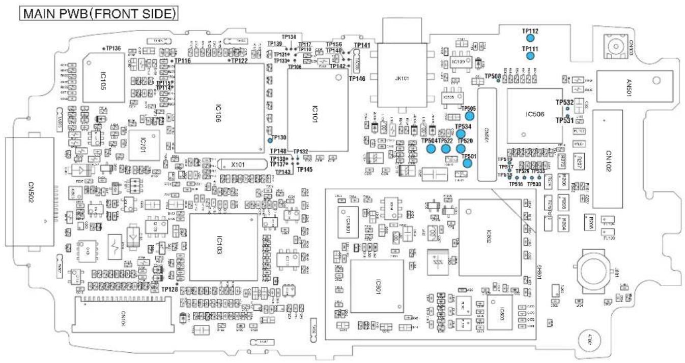
text_image
MAIN PWB(FRONT SIDE) IC105 IC106 X101 CN502 TP136 TP116 TP122 TP134 TP139 TP140 TP141 TP138 TP137 TP145 TP130 TP148 TP132 TP137 TP143 TP146 JK101 TP508 TP504 TP522 TP520 TP501 TP534 TP532 TP531 TP530 TP529 TP533 TP518 TP530 TP508 TP504 TP522 TP520 TP508 TP504 TP522 TP520 TP508 TP504 TP522 TP520 TP508 TP504 TP522 TP520 TP508 TP504 TP522 TP520 TP508 TP504 TP522 TP508 TP504 TP522 TP520 TP508 TP504 TP522 TP520 TP508 TP504 TP522 TP520 TP508 TP504 TP522 TP520 TP508 TP504 TP522 TP521 TP508 TP504 TP522 TP521 TP508 TP504 TP522 TP521 TP508 TP504 TP522 TP521 TP508 TP504 TP522 TP521 TP508 TP504 TP522 TP520 TP508 TP504 TP522 TP521 TP508 TP504 TP522| TP No. Signal name TP No. Signal name | ||
| TP111 VVIB TP505 DGND | ||
| TP112 DGND TP520 BATT | ||
| TP501 BATT TP522 POWONKEY | ||
| TP504 DGND TP534 BATT_SENSE |
CONFIDENTIAL
MAIN PWB-B (REAR SIDE)

geo
| Label | Type | |---|---| | TP127 | Blue Circle | | TP183 | Blue Circle | | TP126 | Blue Circle | | TP113 | Blue Circle | | TP514 | Blue Circle | | TP502 | Blue Circle | | TP503 | Blue Circle | | TP163 | Blue Circle | | TP121 | Blue Circle | | TP160 | Blue Circle | | TP162 | Blue Circle | | TP168 | Blue Circle | | TP123 | Blue Circle | | TP167 | Blue Circle | | TP155 | Blue Circle | | TP104 | Blue Circle | | TP107 | Blue Circle | | TP105 | Blue Circle | | TP526 | Blue Circle | | TP535 | Blue Circle | | TP523 | Blue Circle | | TP524 | Blue Circle | | TP101 | Blue Circle | | TP102 | Blue Circle | | TP135 | Blue Circle | | TP188 | Blue Circle | | TP184 | Blue Circle | | TP170 | Blue Circle | | TP181 | Blue Circle | | TP528 | Blue Circle | | TP527 | Blue Circle | | TP157 | Blue Circle | | TP506 | Blue Circle | | TP177 | Blue Circle | | TP171 | Blue Circle | | TP124 | Blue Circle | | TP172 | Blue Circle | | TP537 | Blue Circle | | TP166 | Blue Circle | | TP538 | Blue Circle | | TP118 | Blue Circle | | TP108 | Blue Circle | | TP103 | Blue Circle | | TP515 | Blue Circle | | TP152 | Blue Circle | | TP151 | Blue Circle | | TP150 | Blue Circle | | TP149 | Blue Circle | | TP125 | Blue Circle | | TP802 | Blue Circle | | TP179 | Blue Circle | | TP164 | Blue Circle | | TP165 | Blue Circle | | TP176 | Blue Circle | | TP521 | Blue Circle | | TP169 | Blue Circle | | TP120 | Blue Circle | | SPX23 | Green Box (Bottom) | | SPX20 | Green Box (Bottom) | | SPX20 | Green Box (Bottom) | | SPX20 | Green Box (Bottom) | | SPX20 | Green Box (Bottom) | | SPX20 | Green Box (Bottom) | | SPX20 | Green Box (Bottom) | | SPX20 | Green Box (Bottom) | | SPX20 | Green Box (Bottom) | | SPX20 | Green Box(Bottom) | | SPX20 | Green Box(Bottom) | | SPX20 | Green Box(Bottom) | | SPX20 | Green Box(Bottom) | | SPX20 | Green Box(Bottom) | | SPX20 | Green Box(Bottom) | | SPX20 | Green Box(Bottom) | | SPX20 | Green Box(Bottom) | | SPX20 | Green Box(Bottom) | | | SPX20 | Green Box(Bottom) | | | SPX20 | Green Box(Bottom) | | | SPX20 | Green Box(Bottom) | | | SPX20 | Green Box(Bottom) | | | SPX20 | Green Box(Bottom) | | | SPX20 | Green Box(Bottom) | | | SPX20 | Green Box(Bottom) | | | SPX20 | Green Box (Bottom) | | | SPX20 | Green Box (Bottom) | | | SPX20 | Green Box (Bottom) | | | SPX20 | Green Box (Bottom) | | | SPX20 | Green Box (Bottom) | | | SPX20 | Green Box (Bottom) | | | SPX20 | Green Box (Bottom) | | | SPX20 | Green Box (Bottom) | | | SPX25 | Green Box (Bottom) | | | SPX25 | Green Box (Bottom) | | | SPX25 | Green Box (Bottom) | | | SPX25 | Green Box (Bottom) | | | SPX25 | Green Box (Bottom) | | | SPX25 | Green Box (Bottom) | | | SPX25 | Green Box (Bottom) | | | SPX25 | Green Box (Bottom) | | | | SPX25 | Green Box (Bottom) | | | | SPX25 | Green Box (Bottom) | | | | SPX25 | Green Box (Bottom) | | | | SPX25 | Green Box (Bottom) | | | | SPX25 | Green Box (Bottom) | | | | SPX25 | Green Box (Bottom) | | | | SPX25 | Green Box (Bottom) | | | | SPX25 | Green Box (Bottom) | | | | SPX25 | Green Box (Bottom) | | | | SPX25 | Green Box (Bottom) | | | | SPX25 | Green Box (Bottom) | | | | SPX25 | Green Box (Bottom) | | | | SPX25 | Green Box (Bottom) | | | | SPX25 | Green Box (Bottom) | | | | SPX38 | Red Dot (Top Right) | | TP538 | Red Dot (Top Right) | | TP180 | Red Dot (Top Right) | | TP188 | Red Dot (Top Right) | | TP187 | Red Dot (Top Right) | | TP186 | Red Dot (Top Right) | | TP185 | Red Dot (Top Right) | | | TP536: Top Right TP535: Top Right TP534: Top Right TP533: Top Right TP532: Top Right TP531: Top Right TP530: Top Right TP529: Top Right TP528: Top Right TP527: Top Right TP526: Top Right TP525: Top Right TP524: Top Right TP523: Top Right TP522: Top Right TP521: Top Right TP520: Top Right TP519: Top Right TP518: Top Right TP517: Top Right TP516: Top Right TP515: Top Right TP514: Top Right TP513: Top Right TP512: Top Right TP511: Top Right TP510: Top Right TP509: Top Right TP508: Top Right TP507: Top Right TP506: Top Right TP505: Top Right TP504: Top Right TP503: Top Right TP502: Top Right TP501: Top Right TP49: Top Right TP48: Top Right TP47: Top Right TP46: Top Right TP45: Top Right TP44: Top Right TP43: Top Right TP42: Top Right TP41: Top Right TP40: Top Right TP39: Top Right TP38: Top Right TP37: Top Right TP36: Top Right TP35: Top Right TP34: Top Right TP33: Top Right TP32: Top Right TP31: Top Right TP30: Top Right TP29: Top Right TP28: Top Right TP27: Top Right TP26: Top Right TP25: Top Right TP24: Top Right TP23: Top Right TP22: Top Right TP21: Top Right TP20: Top Right TP19: Top Right TP18: Top Right TP17: Top Right TP16: Top Right TP15: Top Right TP14: Top Right TP13: Top Right TP12: Top Right TP11: Top Right TP10: Top Right TP9: Top Right TP8: Top Right| TP No. Signal name TP No. Signal name | ||
| TP103 USC [0] TP171 VCORE (1.8V) | ||
| TP104 USC [1] TP172 VAPP | ||
| TP105 USC [2] TP173 VINT (3V) | ||
| TP107 USC [4] TP174 LIGHT3 (KEYLED) | ||
| TP108 USC [5] TP176 VMIC | ||
| TP109 USC [6] TP177 AUXADC1 | ||
| TP113 VVIB TP178 TEMP | ||
| TP118 USC [3] TP179 AUXADC1 | ||
| TP119 MIC TP180 CHGIN_A (5.2V) | ||
| TP120 AUDIO_IN TP181 Flexible PWB insert check terminal 1 | ||
| TP121 JACK_L TP182 Flexible PWB insert check terminal 2 | ||
| TP123 RESET TP183 Flexible PWB insert check terminal 3 | ||
| TP124 PWRON TP184 Flexible PWB insert check terminal 4 | ||
| TP126 SP1 TP502 VBAT | ||
| TP127 SP2 TP503 VBAT | ||
| TP144 Terminal for STACK MEMORY adhesion check 1 | TP506 BATT_SENSE | |
| TP147 Terminal for STACK MEMORY adhesion check 2 | TP514 BT_VCC (3.0V) | |
| TP153 VPP Flash TP515 VBUS_IN | ||
| TP157 Analog Power Supply IC INT | TP521 POWONKEY | |
| TP158 VINT (3V) | TP523 USB D+ | |
| TP160 HEDSET_DET | TP524 USB D- | |
| TP161 STEREO_SW | TP525 RTS | |
| TP162 REMOTE_SW | TP526 CTS | |
| TP163 JACK_R TP527 DGND | ||
| TP164 VABB | TP528 DGND | |
| TP165 VT (2.75V) | TP535 Reserved | |
| TP166 VUSB | TP536 ManufactUre Specific | |
| TP167 VRTC (1.8V) | TP537 CHGIN | |
| TP168 VBACK (3V) | TP801 VTCXO (2.9V) | |
| TP169 VSIM (2.85V) | TP802 VRF (2.9V) | |
| TP170 VMEM (2.8V) | ||
CONFIDENTIAL

text_image
LCD PWB (FRONT SIDE) CN704 CN705 IC708 TP719 IC704 TP718 TP703 CN703 SH701 IC705 IC707 TP704| TP No. Signal name TP No. Signal name | ||
| TP703 SP1 TP704 SP2 |
CONFIDENTIAL
LCD PWB (REAR SIDE)

text_image
TP720 TP709 TP705 TP706 TP711 TP710 TP707 TP708 TP721 TP734 TP723 TP724 TP735 TP722 TP715 TP716 TP712 TP714 TP739 TP729 TP738 TP701 TP713 TP702 TP726 TP725 TP733 TP727 TP732 TP717 TP728 TC16 TC28 TC41 CN701| TP No. Signal name TP No. Signal name | ||
| TP701 SP1 TP720 VDD2 | ||
| TP702 SP2 TP721 RECIVER_OUT+ | ||
| TP705 Backlight 4 TP722 RECIVER_OUT | - | |
| TP706 Backlight 3 TP723 Terminal for LCDC adhesion check 3 | ||
| TP707 Backlight 2 TP724 Terminal for LCDC adhesion check 4 | ||
| TP708 Flash (LED-) TP725 Terminal for APPLICATION POWER adhesion check | ||
| TP709 VLCD_INT (3.0V) TP726 Power supply for camera ( | -8 V) | |
| TP710 Backlight & Flash (LED+) TP727 Power supply for camera (+15V) | ||
| TP711 Backlight 1 TP728 VDD2 (3V) | ||
| TP712 CAMCLK TP729 VBAT | ||
| TP713 13MHzCLK TP733 VDD1 (1.8V) | ||
| TP714 VLCD (1.8V) TP734 RECIVER_OUT+ | ||
| TP715 Terminal for LCDC adhesion check 1 TP735 RECIVER_OUT | - | |
| TP716 Terminal for LCDC adhesion check 2 | TP738 VBAT | |
| TP717 VOUT (External Display) | ||
CONFIDENTIAL
[3] TROUBLESHOOTING
- Power is not turned on.
- Voice transmission/recording is impossible.
- No voice is heard from the earpiece.
- Battery does not charge.
- Vibrator does not work.
- Clock Settings are reset.
- Speaker does not work.
- MP3 cannot be played.
- Video/Voice Recorder playback is impossible.
-
Back Light does not turn on.
-
Out of range and incoming/outgoing calls are impossible.
- The display does not appear on Main Display.
- The display does not appear on External Display (in 65K color mode).
- Pictures cannot be taken.
- AF does not move.
- SIM card is not recognized.
- SD (Memory) card is not recognized.
- USB connection is impossible.
- Bluetooth communication is impossible.
1. POWER IS NOT TURNED ON.
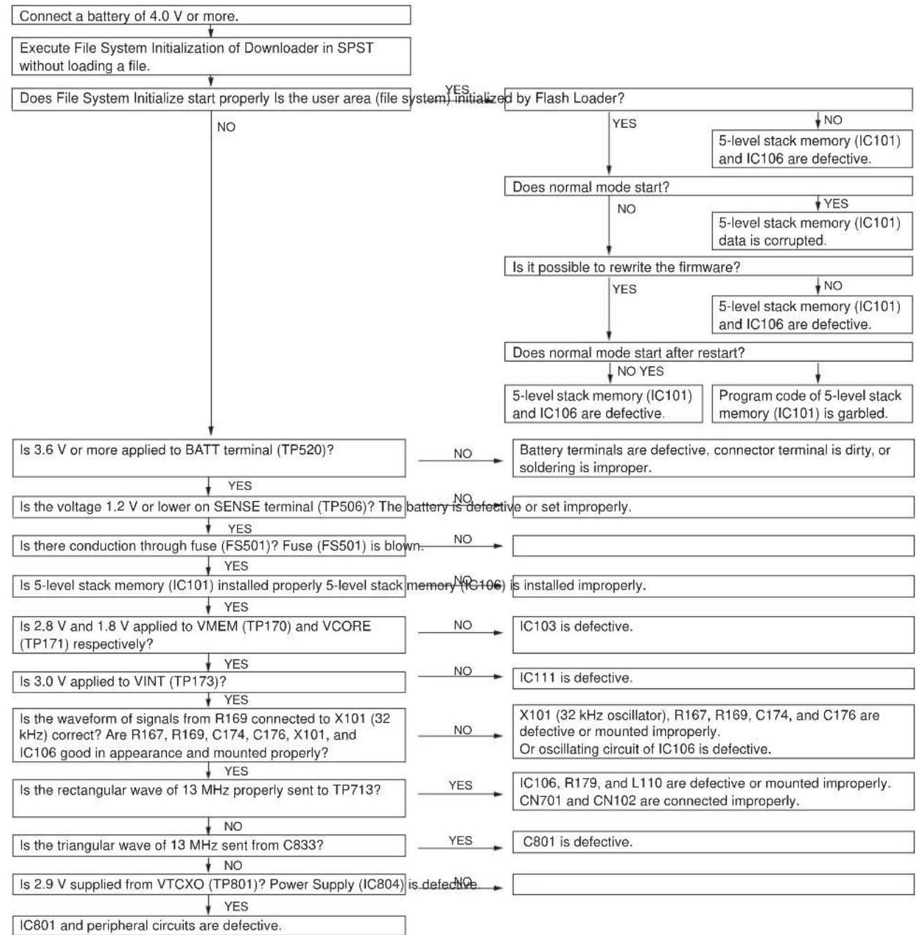
flowchart
graph TD
    A["Connect a battery of 4.0 V or more."] --> B["Execute File System Initialization of Downloader in SPST without loading a file."]
    B --> C{Does File System Initialize start properly is the user area (file system) initialized by Flash Loader?}
    C -->|YES| D{Does normal mode start?}
    C -->|NO| E["Is 3.6 V or more applied to BATT terminal (TP520)?"]
    D -->|YES| F{Battery terminals are defective, connector terminal is dirty, or soldering is improper.}
    D -->|NO| G{Battery terminals are defective, connector terminal is dirty, or soldering is improper.}
    E -->|YES| H{Is the voltage 1.2 V or lower on SENSE terminal (TP506)? The battery is defective or set improperly.}
    E -->|NO| I{Is there conduction through fuse (FS501)? Fuse (FS501) is blown.}
    I -->|YES| J{Is 5-level stack memory (IC101) installed properly 5-level stack memory (IC106) is installed improperly.}
    I -->|NO| K{Is 2.8 V and 1.8 V applied to VMEM (TP170) and VCORE (TP171) respectively?}
    J -->|YES| L{Is 3.0 V applied to VINT (TP173)?}
    J -->|NO| M{Is the waveform of signals from R169 connected to X101 (32 kHz) correct? Are R167, R169, C174, C176, X101, and IC106 good in appearance and mounted properly?}
    M -->|YES| N{Is the rectangular wave of 13 MHz properly sent to TP713?}
    M -->|NO| O{Is the triangular wave of 13 MHz sent from C833?}
    N -->|YES| P{Is 2.9 V supplied from VTCXO (TP801)? Power Supply (IC804) is defective.}
    N -->|NO| Q{Is the voltage 1.2 V or lower on SENSE terminal (TP506)? The battery is defective or set improperly.}
    O -->|YES| R{Is the voltage 3.6 V or more applied to BATT terminal (TP520)?}
    O -->|NO| S{Is there conduction through fuse (FS501)? Fuse (FS501) is blown.}
    S -->|YES| T{Is 2.8 V and 1.8 V applied to VMEM (TP170) and VCORE (TP171) respectively?}
    S -->|NO| U{Is the rectangular wave of 13 MHz properly sent to TP713?}
    U -->|YES| V{Is the triangular wave of 13 MHz sent from C833?}
    U -->|NO| W{Is the triangular wave of 13 MHz sent from C833?}
    W -->|YES| X{Is 2.9 V supplied from VTCXO (TP801)? Power Supply (IC804) is defective.}
    W -->|NO| Y{Is the triangular wave of 13 MHz sent from C833?}
    X -->|YES| Z{Is the triangular wave of 13 MHz sent from C833?}
    X -->|NO| AA{Is the triangular wave of 13 MHz sent from C833?}
    X -->|YES| AB{Is the triangular wave of 13 MHz sent from C833?}
TM200 1ADJUSTMENTS, PERFORMANCE CHECK, AND FIRMWARE UPGRADE
CONFIDENTIAL
2. VOICE TRANSMISSION/RECORDING IS IMPOSSIBLE.
Phone

flowchart
graph TD
    A["Replace the microphone. Is the problem solved?"] -->|NO| B["Is 1.2 - 2.1 V applied to both ends of C101?"]
    A -->|YES| C["The built-in microphone is defective or in a poor contact with the PWB."]
    B -->|NO| D["Is 1.2 - 2.1 V applied to TP119?"]
    B -->|YES| E["Is 2.4 - 2.5 V applied to TP176?"]
    E -->|NO| F["R125 is defective."]
    E -->|YES| G["Is 2.4 - 2.5 V applied to IC103 pin 76?"]
    G -->|NO| H["IC103 is defective."]
    G -->|YES| I["R115 and C108 are defective."]
    D -->|YES| J["Is approx. 1.7 V applied to IC103 pin 80? Is approx. 1.7 V applied to IC103 pin 96?"]
    D -->|YES| K["Is 2.7 or more voltage applied to R192 (IC106 pin 89 side)? R192 is defective. (Headset mode is set.)"]
    K -->|NO| L["Replace C126 or C133. Is the problem solved?"]
    K -->|YES| M["C126 or C133 is defective."]
    L -->|NO| N["IC103 and IC106 are defective."]
    L -->|YES| O["IC103 is defective."]
Hands free kit (headset)
(The following procedure applies to both monaural and stereo headsets.)

flowchart
graph TD
    A["Replace the hands free kit. Is the signal sent? Hands free kit is defective."] -->|YES| B["C104, R112, and V101 are defective."]
    A -->|NO| C["Is 0.7 - 1.8 V applied to JK101 pin 2? Is 0.7 - 1.8 V applied to TP120?"]
    C -->|YES| D["Is approx. 1.7 V applied to IC103 pin 79? Is approx. 1.7 V applied to IC103 pin 95?"]
    C -->|NO| E["Is 2.4 - 2.5 V applied to TP176?"]
    E -->|YES| F["R122 is defective."]
    E -->|NO| G["Is 2.4 - 2.5 V applied to IC103 pin 76?"]
    G -->|YES| H["R115 and C108 are defective."]
    G -->|NO| I["IC103 is defective."]
    I -->|YES| J["R262 and R129 are defective."]
    I -->|NO| K["Is the voltage 0 V on R192 (IC106 pin 89 side)?"]
    K -->|YES| L["Replace C127 or C134. Is the problem solved? C127 or C134 is defective."]
    K -->|NO| M["Replace JK101. Is the problem solved?"]
    M -->|YES| N["JK101 is defective, or the jack plug pin 2 is in a poor contact with hands free kit."]
    M -->|NO| O["IC103 and IC106 are defective."]
CONFIDENTIAL
3. NO VOICE IS HEARD FROM THE EARPIECE.
Phone
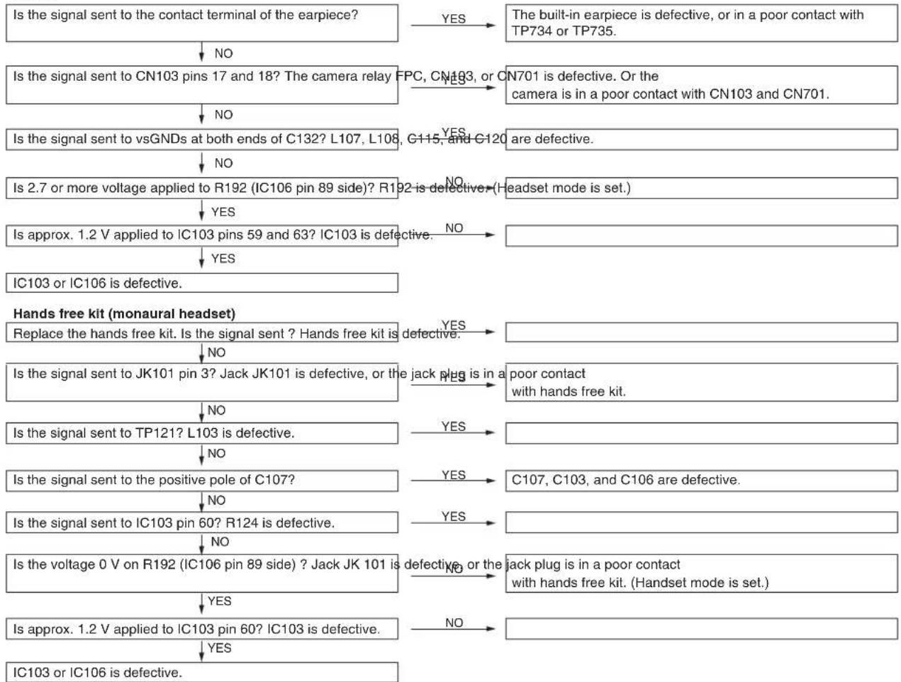
flowchart
graph TD
    A["Is the signal sent to the contact terminal of the earpiece?"] -->|YES| B["The built-in earpiece is defective, or in a poor contact with TP734 or TP735."]
    A -->|NO| C["Is the signal sent to CN103 pins 17 and 18? The camera relay"]
    C -->|YES| D["FPC, CN103, or CN701 is defective. Or the camera is in a poor contact with CN103 and CN701."]
    C -->|NO| E["Is the signal sent to vsGNDs at both ends of C132? L107, L108, C115, and C120 are defective."]
    E -->|YES| F["Is 2.7 or more voltage applied to R192 (IC106 pin 89 side)? R192 is defective (Headset mode is set.)"]
    E -->|NO| G["Is approx. 1.2 V applied to IC103 pins 59 and 63? IC103 is defective."]
    G -->|YES| H["IC103 or IC106 is defective."]
    G -->|NO| I["Is approx. 1.2 V applied to IC103 pin 60? IC103 is defective."]
    I -->|YES| J["IC103 or IC106 is defective."]
    I -->|NO| K["Is approx. 1.2 V applied to IC103 pin 60? IC103 is defective."]
    K -->|YES| L["Is the signal sent to JK101 pin 3? Jack JK101 is defective, or the jack plug is in a poor contact with hands free kit."]
    K -->|NO| M["Is the signal sent to TP121? L103 is defective."]
    M -->|YES| N["Is the signal sent to the positive pole of C107?"]
    M -->|NO| O["Is the signal sent to IC103 pin 60? R124 is defective."]
    O -->|YES| P["Is the voltage 0 V on R192 (IC106 pin 89 side)? Jack JK 101 is defective, or the jack plug is in a poor contact with hands free kit. (Handset mode is set.)"]
    O -->|NO| Q["Is approx. 1.2 V applied to IC103 pin 60? IC103 is defective."]
    Q -->|YES| R["IC103 or IC106 is defective."]
    Q -->|NO| S["Is approx. 1.2 V applied to IC103 pin 60? IC103 is defective."]
Hands free kit (stereo headset) - Option
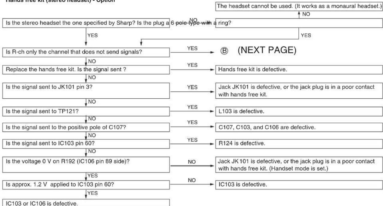
flowchart
graph TD
    A["Is the stereo headset the one specified by Sharp? Is the plug a 6 pole type with a ring?"] -->|NO| B["Is R-ch only the channel that does not send signals?"]
    A -->|YES| C["Is R-ch only the channel that does not send signals?"]
    B -->|YES| D["Replace the hands free kit. Is the signal sent?"]
    B -->|NO| E["Is the signal sent to JK101 pin 3?"]
    D -->|YES| F["Hands free kit is defective."]
    E -->|YES| G["Jack JK101 is defective, or the jack plug is in a poor contact with hands free kit."]
    E -->|NO| H["Is the signal sent to TP121?"]
    H -->|YES| I["L103 is defective."]
    H -->|NO| J["Is the signal sent to the positive pole of C107?"]
    J -->|YES| K["C107, C103, and C106 are defective."]
    J -->|NO| L["Is the signal sent to IC103 pin 60?"]
    L -->|YES| M["R124 is defective."]
    L -->|NO| N["Is the voltage 0 V on R192 (IC106 pin 89 side)?"]
    N -->|NO| O["Jack JK101 is defective, or the jack plug is in a poor contact with hands free kit. (Handset mode is set.)"]
    N -->|YES| P["Is approx. 1.2 V applied to IC103 pin 60?"]
    N -->|NO| Q["IC103 is defective."]
    P -->|YES| R["IC103 or IC106 is defective."]
    P -->|NO| S["Is approximate 1.2 V applied to IC103 pin 60?"]
    S -->|YES| T["IC103 or IC106 is defective."]
CONFIDENTIAL

flowchart
graph TD
    A["(BACK PAGE)"] --> B["Is the signal sent to JK101 pin 1? Jack JK101 is defective, or the jack plug is in a poor contact with hands free kit."]
    B -->|NO| C["Is the signal sent to TP163? L105 is defective."]
    C -->|NO| D["Is the signal sent to the positive pole of C110? C110, C105, and G109 are defective."]
    D -->|NO| E["Is the signal sent to IC103 pin 64? R126 is defective."]
    E -->|NO| F["Is the voltage 0.1 V or lower on R191 (IC106 pin 100 side)?"]
    F -->|YES| G["Is approx. 1.2 V applied to IC103 pin 64? IC103 is defective."]
    G -->|YES| H["IC103 or IC106 is defective."]
    G -->|NO| I["Jack JK101 is defective, or the jack plug is in a poor contact with hands free kit. (Monaural mode is set.)"]
    I -->|NO| J[" "]
4. BATTERY DOES NOT CHARGE.
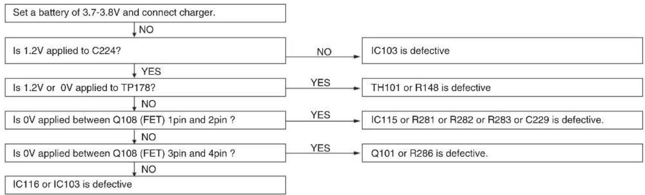
flowchart
graph TD
    A["Set a battery of 3.7-3.8V and connect charger."] -->|NO| B["Is 1.2V applied to C224?"]
    B -->|YES| C["Is 1.2V or 0V applied to TP178?"]
    C -->|NO| D["Is 0V applied between Q108 (FET) 1pin and 2pin ?"]
    D -->|NO| E["Is 0V applied between Q108 (FET) 3pin and 4pin ?"]
    E -->|NO| F["IC116 or IC103 is defective"]
    B -->|NO| G["IC103 is defective"]
    C -->|YES| H["TH101 or R148 is defective"]
    D -->|YES| I["IC115 or R281 or R282 or R283 or C229 is defective."]
    E -->|YES| J["Q101 or R286 is defective."]
5. VIBRATOR DOES NOT WORK.

flowchart
graph TD
    A["Are vibrator terminals in contact with the land? Are terminals and the land clean?"] -->|YES| B["Is rectangular wave of 3 V sent to between Vibrator terminals in sync with the vibration pattern?"]
    B -->|NO| C["Is VBAT voltage applied to IC109 pin 5? IC109 is soldered improperly."]
    C -->|YES| D["Is signal synchronized with the vibration pattern sent to IC109 pin 1?"]
    D -->|NO| E["Is signal synchronized with the vibration pattern sent from IC105 pin 19?"]
    E -->|NO| F["Is approx. 3 V applied to IC105 pin 7? C167 and C168 good in appearance and mounted properly?"]
    F -->|YES YES| G["IC105 is defective, or the control signal line to IC106 is defective."]
    G -->|NO| H["C167 and C168 are defective."]
    H -->|NO| I["IC105 is defective, or the control signal line to IC106 is defective."]
    I --> J["Is proportional 3 V applied to IC105 pin 7? C167 and C168 good in appearance and mounted properly?"]
    J --> K["Is signal synchronized with the vibration pattern sent from IC105 pin 19?"]
    K -->|YES| L["IC109 is defective."]
    L --> M["Vibrator is defective."]
    M --> N["Vibrator is deformed and defective. (When vibrator terminals and the land are dirty, clean or replace them.)"]
CONFIDENTIAL
6. CLOCK SETTING ARE RESET.
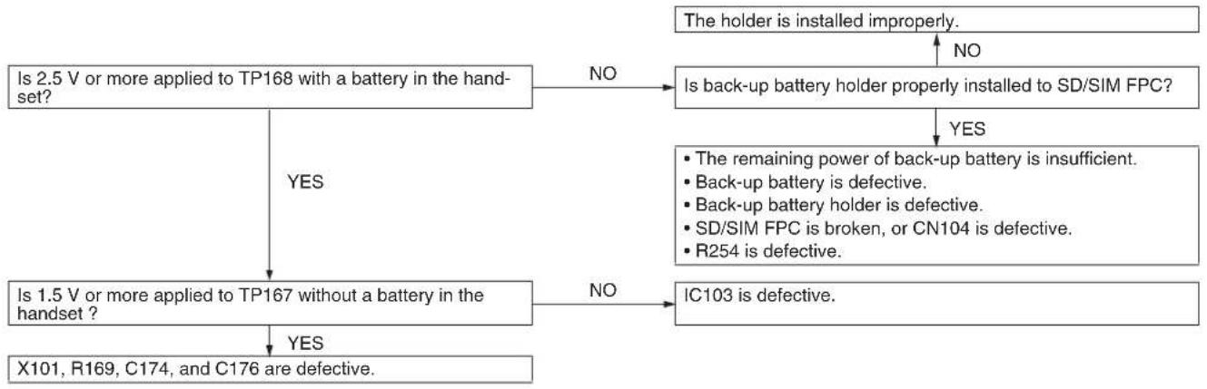
flowchart
graph TD
    A["Is 2.5 V or more applied to TP168 with a battery in the handset?"] -->|NO| B["Is back-up battery holder properly installed to SD/SIM FPC?"]
    B -->|YES| C["Is 1.5 V or more applied to TP167 without a battery in the handset?"]
    C -->|NO| D["IC103 is defective."]
    A -->|YES| E["X101, R169, C174, and C176 are defective."]
    B -->|NO| F["The holder is installed improperly."]
    C -->|YES| G["• The remaining power of back-up battery is insufficient.<br>• Back-up battery is defective.<br>• Back-up battery holder is defective.<br>• SD/SIM FPC is broken, or CN104 is defective.<br>• R254 is defective."]
7. SPEAKER DOES NOT WORK.
* When ring tones sound, but keypad tones do not, "Keypad Tones" is set to Off.
* When Ringer Volume is set to "Silent":
- Voice Recorder playback sound is not produced.
· Playback sound of Video and MP3 can be heard by increasing the volume during playback.
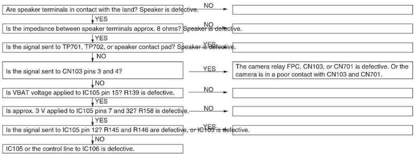
flowchart
graph TD
    A["Are speaker terminals in contact with the land? Speaker is defective."] -->|NO| B["Is the impedance between speaker terminals approx. 8 ohms?"]
    B -->|YES| C["Is the signal sent to TP701, TP702, or speaker contact pad?"]
    C -->|NO| D["Is the signal sent to CN103 pins 3 and 4?"]
    D -->|YES| E["Is VBAT voltage applied to IC105 pin 15? R139 is defective."]
    E -->|NO| F["Is approx. 3 V applied to IC105 pins 7 and 32? R158 is defective."]
    F -->|NO| G["Is the signal sent to IC105 pin 12? R145 and R146 are defective, or IC105 is defective."]
    G -->|YES| H["IC105 or the control line to IC106 is defective."]
    G -->|YES| I["The camera relay FPC, CN103, or CN701 is defective. Or the camera is in a poor contact with CN103 and CN701."]
CONFIDENTIAL
8. MP3 CANNOT BE PLAYED.
Speaker

flowchart
graph TD
    A["Is Ringer Volume set to "Silent"?ancel "SC ilent". Is sound produced?"] -->|YES| B["No"]
    A -->|NO| C["Is output of the video and voice recorder normal? Are keypad tones and ring tones normal?"]
    C -->|YES| D["Insert an SD card with MP3 files recorded on a normal unit. Do they play?"]
    C -->|NO| E["Is the SD card recognized?"]
    D -->|YES| F["Is the signal sent to IC103 pin 60? Parts between IC103 pin 60"]
    D -->|NO| G["IC103 is defective."]
    E -->|YES| H["Go to the section "Video/Voice Recorder playback is impossible.""]
    E -->|NO| I["Go to the section "Speaker does not work.""]
    F -->|YES| J["Go to the section "SD (Memory) card is not recognized.""]
    F -->|NO| K["IC103 is defective."]
    G -->|YES| L["4 & 13 are defective or soldered improperly."]
    H --> M["Not defective."]
    I --> N["Not defective."]
Hands free kit (headset)
(The following procedure applies to both monaural and stereo headsets.)

flowchart
graph TD
    A["Is sound normally produced from Speaker? Go to the section regarding Speaker."] --> B{No}
    B --> C["Replace the hands free kit. Is sound produced? Hands free kit is defective."]
    C --> D{YES}
    D --> E["Go to "Hands free kit (monaural headset)" in the section "No voice is heard from the earpiece.""]
    E --> F["NO"]
flowchart
graph TD
    A["Are keypad tones and ring tones normal? Go to the section "Speaker does not work.""] -->|YES| B["In Playback window, does playback start normally and the capacity bar change?"]
    B -->|NO| C["IC101 or IC106 is defective."]
    C -->|YES| D["Is Ringer Volume set to "Silent"? Cancel "Silent". Is sound produced?"]
    D -->|NO| E["Is the signal sent to IC103 pin 60?"]
    E -->|YES| F["Parts between IC103 pin 60 and IC105 pins 14 & 13 are defective or soldered improperly."]
    F -->|NO| G["IC103 is defective."]
    F -->|YES| H["Not defective."]
Hands free kit (headset)
* If R-ch is the only channel of stereo headset that does not send signals, see "Hands free kit (stereo headset)" in the section "No voice is heard from the earpiece."
flowchart
graph TD
A["Replace the hands free kit.<br>Is the signal sent?"] -->|NO| B["In Playback window, does playback start normally and the capacity bar change?"]
B -->|YES| C["Is Ringer Volume set to "Silent"? Cancel "Silent". Is sound produced?"]
B -->|NO| D["Hands free kit is defective."]
C -->|YES| E["Go to "Hands free kit (monaural headset)" in the section "No voice is heard from the earpiece.""]
C -->|NO| F["IC101 or IC106 is defective."]
F -->|YES| G["Not defective."]
F -->|NO| H["End"]
CONFIDENTIAL
- BACK LIGHT DOES NOT TURN ON.
flowchart
graph TD
    A["Is VBAT voltage applied to C738? Is fuse (F702) in good appearance, mounted properly, and is there conduction?"] -->|YES| B["Which back light does not turn on, Main or External?"]
    A -->|NO| C["F702 is mounted improperly, or the fuse is brown."]
    C -->|YES| D["C733, C738, and L703 are defective."]
    D -->|C| E["External display only."]
    E -->|No| F["Is back light setting for External Display set to On? Go to the setting as follows and set it to On: Settings Phone Settings Main Display Back light"]
    F -->|YES| G["Does it turn on?"]
    F -->|NO| H["Is CN705 in good appearance and mounted properly? CN705 is defective."]
    H -->|YES| I["Is the contact point of back light FPC clean? Is back light FPC properly inserted to CN705?"]
    H -->|NO| J["Back light FPC or CN705 is defective."]
    I -->|YES| K["Is 3 - 6 V applied between TP710 and TP705? Is 3 - 6 V applied between TP710 and TP706? Is 3 - 6 V applied between TP710 and TP707? Is 3 - 6 V applied between TP710 and TP711?"]
    J -->|YES| L["Clean back light FPC and insert it again. Does it turn on?"]
    J -->|NO| M["Not defective."]
    K -->|YES| N["Back light FPC is defective."]
    L -->|YES| O["Are C735, C791, C733, C738, C730, C731, R708 and R707 in good appearance and mounted properly?"]
    M -->|YES| P["C735, C791, C733, C738, C730, C731, R708 and R707 are defective."]
    N -->|NO| Q["IC708 are defective."]
    O -->|YES| R["Is back light setting for Sub Display set to On? Go to the setting as follows and set it to On: Settings Phone Settings Main Display Back light"]
    P -->|NO| S["IC708 is defective or mounted improperly."]
    Q -->|YES| T["Is 3-6V applied between LED703 anode (A) terminal and LED704 cathode (K) terminal?"]
    Q -->|NO| U["IC708 is defective or mounted improperly."]
    R -->|YES| V["LED703 and LED704 are defective."]
    R -->|NO| W["Is 3-6V applied between LED703 anode (A) terminal and LED704 cathode (K) terminal?"]
CONFIDENTIAL
11. OUT OF RANGE AND INCOMING/OUTGOING CALLS ARE IMPOSSIBLE.
[Checkpoint s in RF Test Tool]
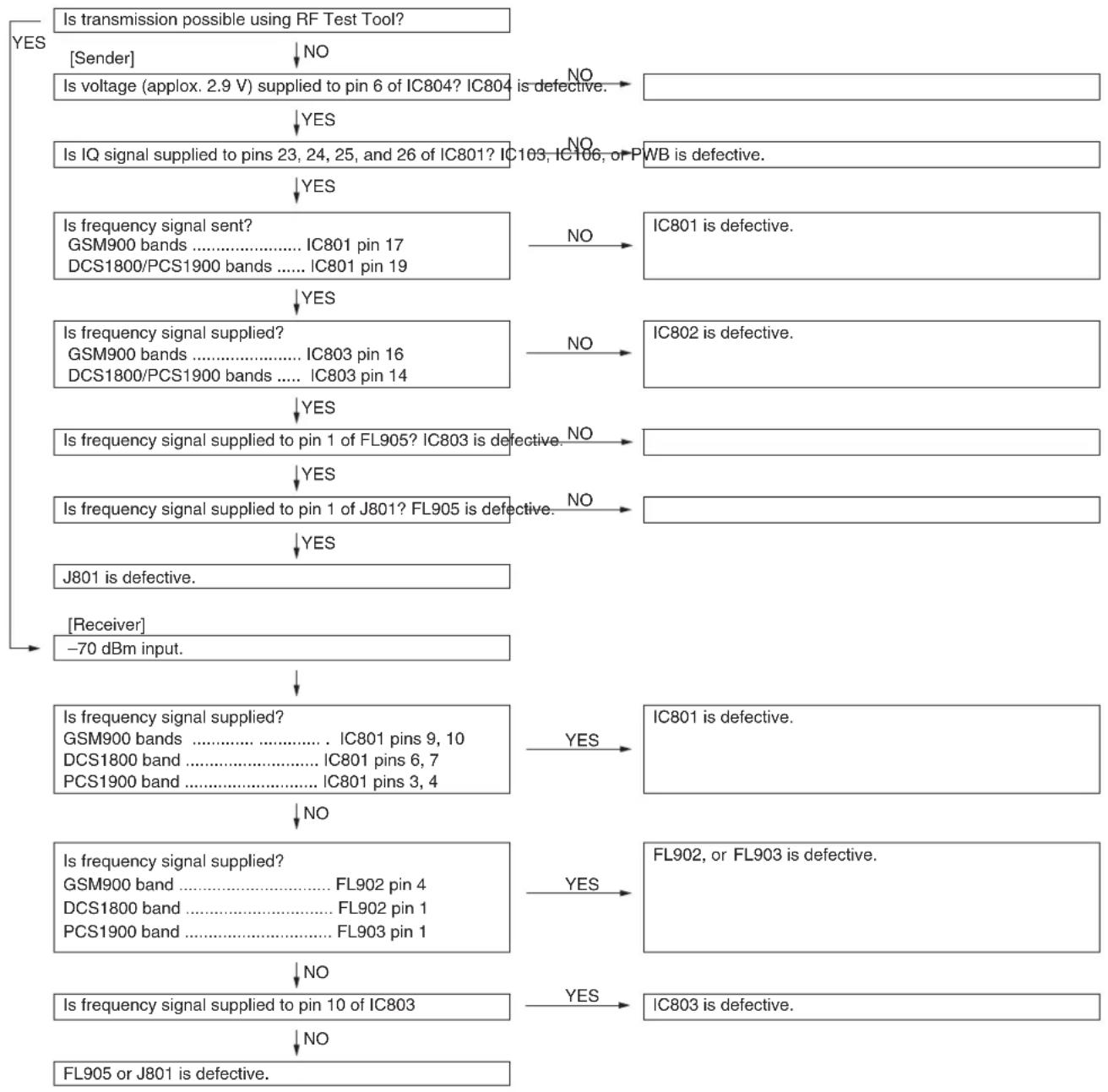
flowchart
graph TD
    A["Is transmission possible using RF Test Tool?"] -->|YES| B["[Sender"]]
    A -->|NO| C["Is voltage (approx. 2.9 V) supplied to pin 6 of IC804? IC804 is defective."]
    C --> D["Is IQ signal supplied to pins 23, 24, 25, and 26 of IC801? IC103, IC106, or WB is defective."]
    D --> E["Is frequency signal sent? GSM900 bands ...... IC801 pin 17 DCS1800/PCS1900 bands ...... IC801 pin 19"]
    E --> F["Is frequency signal supplied? GSM900 bands ...... IC803 pin 16 DCS1800/PCS1900 bands ...... IC803 pin 14"]
    F --> G["Is frequency signal supplied to pin 1 of FL905? IC803 is defective."]
    G --> H["Is frequency signal supplied to pin 1 of J801? FL905 is defective."]
    H --> I["J801 is defective."]
    I --> J["[Receiver"]]
    J --> K["-70 dBm input."]
    K --> L["Is frequency signal supplied? GSM900 bands ...... IC801 pins 9, 10 DCS1800 band ...... IC801 pins 6, 7 PCS1900 band ...... IC801 pins 3, 4"]
    L -->|NO| M["Is frequency signal supplied? GSM900 band ...... FL902 pin 4 DCS1800 band ...... FL902 pin 1 PCS1900 band ...... FL903 pin 1"]
    M --> N["Is frequency signal supplied to pin 10 of IC803"]
    N -->|NO| O["FL905 or J801 is defective."]
    N -->|YES| P["IC803 is defective."]
    P --> Q["IFN902, or FL903 is defective."]
    Q --> R["IC801 is defective."]
    R --> S["IC801 is defective."]
    S --> T["IC802 is defective."]
    T --> U["IC801 is defective."]
CONFIDENTIAL
12. THE DISPAY DOES NOT APPEAR ON MAIN DISPLAY.
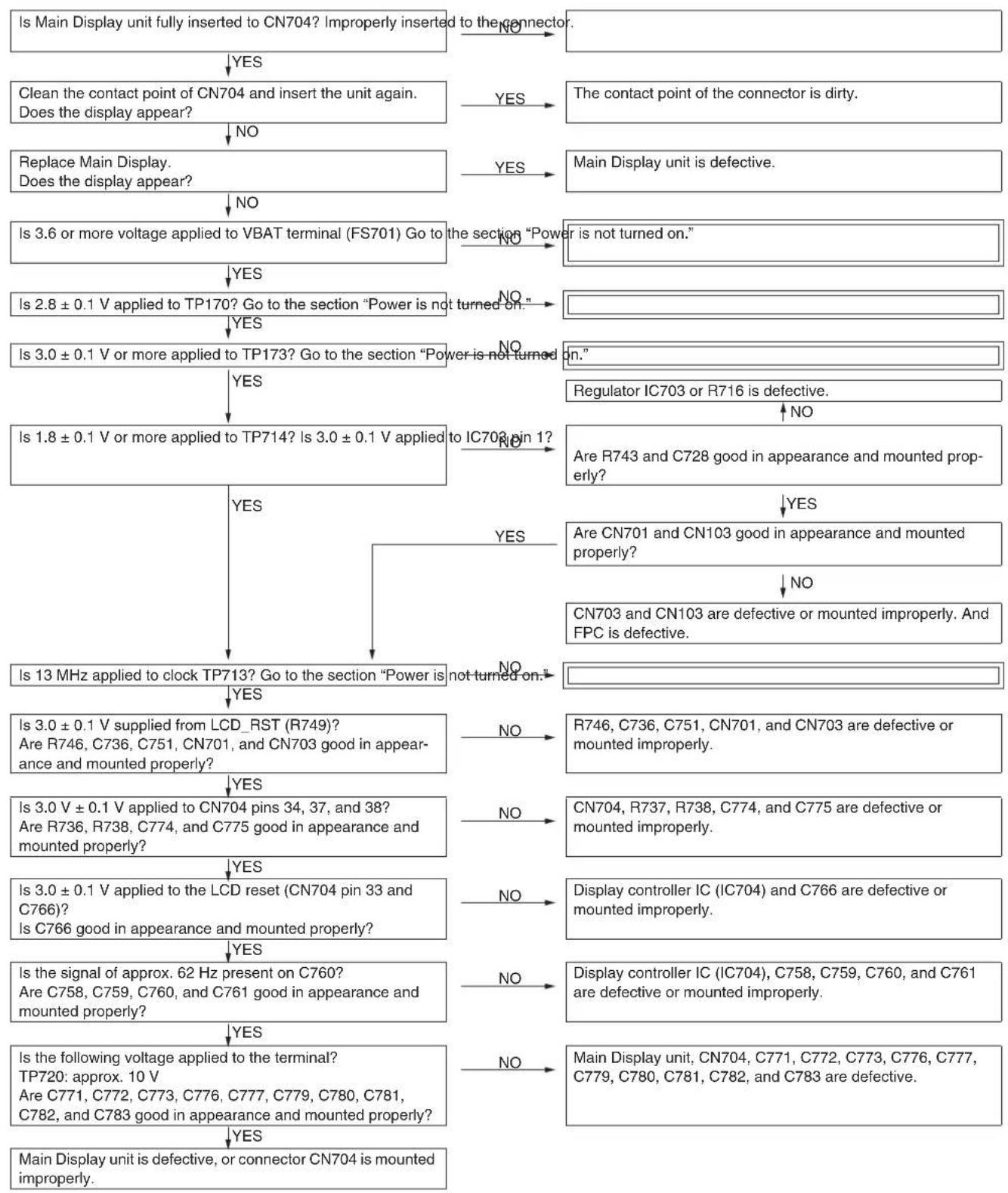
flowchart
Display unit status flowchart for CN704, showing transitions from main display unit to fault points and fault outcomes based on voltage, power, and signal conditions.CONFIDENTIAL
13. THE DISPLAY DOES NOT APPEAR ON EXTERNAL DISPLAY (IN 65K COLOR MODE).
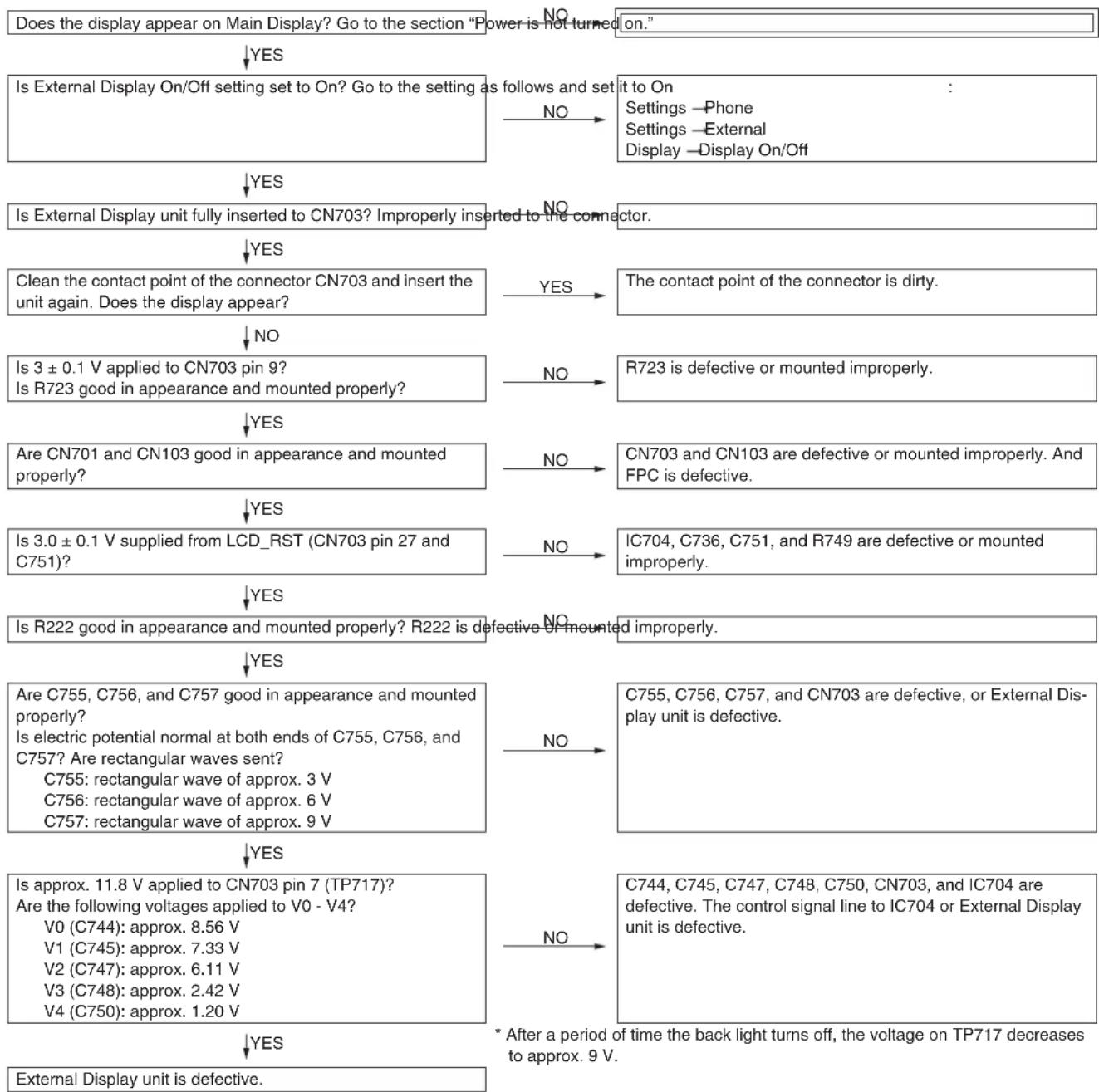
flowchart
graph TD
    A["Does the display appear on Main Display? Go to the section "Power is not turned on.""] --> B{Is External Display On/Off setting set to On? Go to the setting as follows and set it to On}
    B -->|YES| C["Is External Display unit fully inserted to CN703? Improperly inserted to the connector."]
    B -->|NO| D["Is 3 ± 0.1 V applied to CN703 pin 9?"]
    D --> E{Are CN701 and CN103 good in appearance and mounted properly?}
    E -->|YES| F["Is 3.0 ± 0.1 V supplied from LCD_RST (CN703 pin 27 and C751)?"]
    E -->|NO| G["Is R222 good in appearance and mounted properly? R222 is defective or mounted improperly."]
    F --> H{Are C755, C756, and C757 good in appearance and mounted properly?}
    H -->|YES| I["Is approx. 11.8 V applied to CN703 pin 7 (TP717)?"]
    H -->|NO| J["Is electric potential normal at both ends of C755, C756, and C757? Are rectangular waves sent?"]
    I --> K["V0 (C744): approx. 8.56 V"]
    I --> L["V1 (C745): approx. 7.33 V"]
    I --> M["V2 (C747): approx. 6.11 V"]
    I --> N["V3 (C748): approx. 2.42 V"]
    I --> O["V4 (C750): approx. 1.20 V"]
    J --> P["C755, C756, C757, and CN703 are defective, or External Display unit is defective."]
    K --> Q["* After a period of time the back light turns off, the voltage on TP717 decreases to approx. 9 V."]
    L --> Q
    M --> Q
    N --> Q
    O --> Q
CONFIDENTIAL
14. PICTURES CANNOT BE TAKEN.
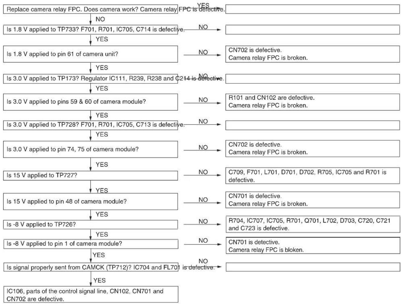
flowchart
graph TD
    A["Replace camera relay FPC. Does camera work? Camera relay FPC is defective."] --> B{Is 1.8 V applied to TP733? F701, R701, IC705, C714 is defective.}
    B -->|NO| C["Is 1.8 V applied to pin 61 of camera unit?"]
    B -->|NO| D["CN702 is defective. Camera relay FPC is broken."]
    C --> E{Is 3.0 V applied to TP173? Regulator IC111, R239, R238 and C214 is defective.}
    E -->|NO| F["R101 and CN102 are defective. Camera relay FPC is broken."]
    E -->|NO| G["Is 3.0 V applied to pins 59 & 60 of camera module?"]
    G --> H{Is 3.0 V applied to TP728? F701, R701, IC705, C713 is defective.}
    H -->|NO| I["Is 3.0 V applied to pin 74, 75 of camera module?"]
    H -->|NO| J["CN702 is defective. Camera relay FPC is broken."]
    H -->|NO| K["Is 15 V applied to TP727?"]
    K --> L{Is 15 V applied to pin 48 of camera module?}
    L -->|NO| M["CN701 is defective. Camera relay FPC is broken."]
    L -->|NO| N["Is -8 V applied to TP726?"]
    N --> O{Is -8 V applied to pin 1 of camera module?}
    O -->|NO| P["R704, IC707, IC705, R701, Q701, L702, D703, C720, C721 and C723 is defective."]
    O -->|NO| Q["Is signal properly sent from CAMCK (TP712)? IC704 and FL701 is defective."]
    Q --> R["IC106, parts of the control signal line, CN102, CN701 and CN702 are defective."]
15. AF DOES NOT MOVE

flowchart
graph TD
    A["Is 3.6 V or more applied to TP729?"] -->|YES| B["Is 36V or more applied to pin7 of camera module?"]
    A -->|NO| C["Go to the dection "Power is not turned on""]
    B -->|YES| D["IC705 or Q702 is defective.<br>Camera relay FPC is broken."]
    B -->|NO| E["L716 and CN702 is defective."]
CONFIDENTIAL
16. SIM CARD IS NOT RECOGNIZED.
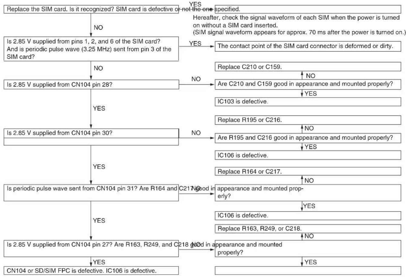
flowchart
graph TD
    A["Replace the SIM card. Is it recognized? SIM card is defective or not the one specified."] --> B{Is 2.85 V supplied from pins 1, 2, and 6 of the SIM card? And is periodic pulse wave (3.25 MHz) sent from pin 3 of the SIM card?}
    B -->|NO| C["Is 2.85 V supplied from CN104 pin 28?"]
    B -->|YES| D{The contact point of the SIM card connector is deformed or dirty.}
    C -->|NO| E["Is 2.85 V supplied from CN104 pin 30?"]
    C -->|YES| F{Replace C210 or C159.}
    E -->|NO| G{Are C210 and C159 good in appearance and mounted properly?}
    E -->|YES| H{IC103 is defective.}
    F -->|NO| I{Are R195 and C216 good in appearance and mounted properly?}
    F -->|YES| J{IC106 is defective.}
    G -->|NO| K{Are R195 and C216 good in appearance and mounted properly?}
    G -->|YES| L{Replace R195 or C216.}
    H -->|NO| M{Are R195 and C216 good in appearance and mounted properly?}
    H -->|YES| N{IC106 is defective.}
    I -->|NO| O{Are R195 and C216 good in appearance and mounted properly?}
    I -->|YES| P{Replace R195 or C216.}
    J -->|NO| Q{Are R195 and C216 good in appearance and mounted properly?}
    J -->|YES| R{IC106 is defective.}
    K -->|NO| S{Are R195 and C216 good in appearance and mounted properly?}
    K -->|YES| T{Replace R195 or C216.}
    L -->|NO| U{Are R164 and C217.}
    L -->|YES| V{Is periodic pulse wave sent from CN104 pin 31? Are R164 and C217 good in appearance and mounted properly?}
    M -->|NO| W{Is periodic pulse wave sent from CN104 pin 31? Are R164 and C217 good in appearance and mounted properly?}
    N -->|NO| X{Is periodic pulse wave sent from CN104 pin 31? Are R164 and C217 good in appearance and mounted properly?}
    O -->|YES| Y{Is 2.85 V supplied from CN104 pin 27? Are R163, R249, and C218 good in appearance and mounted properly?}
    P -->|YES| Z{CN104 or SD/SIM FPC is defective. IC106 is defective.}
    Q -->|NO| AA{Is periodic pulse wave sent from CN104 pin 27? Are R163, R249, and C218 good in appearance and mounted properly?}
    R -->|YES| AA
    R -->|NO| AB{Is periodic pulse wave sent from CN104 pin 27? Are R163, R249, and C218 good in appearance and mounted properly?}
17. SD (MEMORY) CARD IS NOT RECOGNIZED.

flowchart
graph TD
    A["Is the SD card checked for operation? Use an SD card that has been checked."] --> B{YES}
    B -->|No| C["Is the SD card recognized on PC, etc.?"]
    B -->|Yes| D{YES}
    D -->|No| E["Is the card insertion detected? Is SD/SIM FPC properly inserted to CN104?"]
    D -->|YES| F{YES}
    F -->|YES| G["Is 2.75 V or more applied to VAPP? IC103 or Q103 is defective"]
    F -->|NO| H["Does the signal of SD_DET become "L" when the card is inserted?"]
    H --> I{YES}
    I -->|YES| J["IC106 is defective. SD card socket"]
    I -->|NO| K["Reinsert SD/SIM FPC, and try again."]
    J --> L["IC106 is defective. SD card socket and CN104 are in poor contact. Hardwiring on PWB is broken."]
    K --> M["SD card socket and CN104 are in poor contact. SD_CLK, SD_CMD, and SD_DAT [3:0"] on PWB are broken or short-circuited. IC106 is defective or has come off.]
    G --> N{YES}
    N -->|NO| O["Can the SD card be formatted?"]
    N -->|NO| P{YES}
    O --> Q["After formatting, can the SD card be used? IC106 is defective or has come off."]
    P --> R["File system on the SD card is damaged."]
    Q --> S["File system on the SD card is damaged."]
CONFIDENTIAL
- USB CONNECTION IS IMPOSSIBLE.
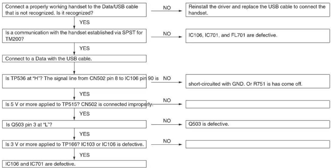
flowchart
graph TD
    A["Connect a properly working handset to the Data/USB cable that is not recognized. Is it recognized?"] -->|YES| B["Is a communication with the handset established via SPST for TM200?"]
    B -->|YES| C["Connect to a Data with the USB cable."]
    C --> D["Is TP536 at "H"? The signal line from CN502 pin 8 to IC106 pin 90 is 90 is NO"]
    D -->|YES| E["Is 5 V or more applied to TP515? CN502 is connected improperly."]
    D -->|NO| F["short-circuited with GND. Or R751 is has come off."]
    E -->|YES| G["Is Q503 pin 3 at "L"?"]
    E -->|NO| H["Q503 is defective."]
    G -->|YES| I["Is 3 V or more applied to TP166? IC103 or IC106 is defective."]
    G -->|NO| J["IC106 and IC701 are defective."]
    H -->|NO| K["No"]
    I -->|YES| L["IC106 and IC701 are defective."]
    J -->|NO| M["No"]
    K --> N["Reinstall the driver and replace the USB cable to connect the handset."]
    L --> O["No"]
- BLUETOOTH COMMUNICATION IS IMPOSSIBLE.
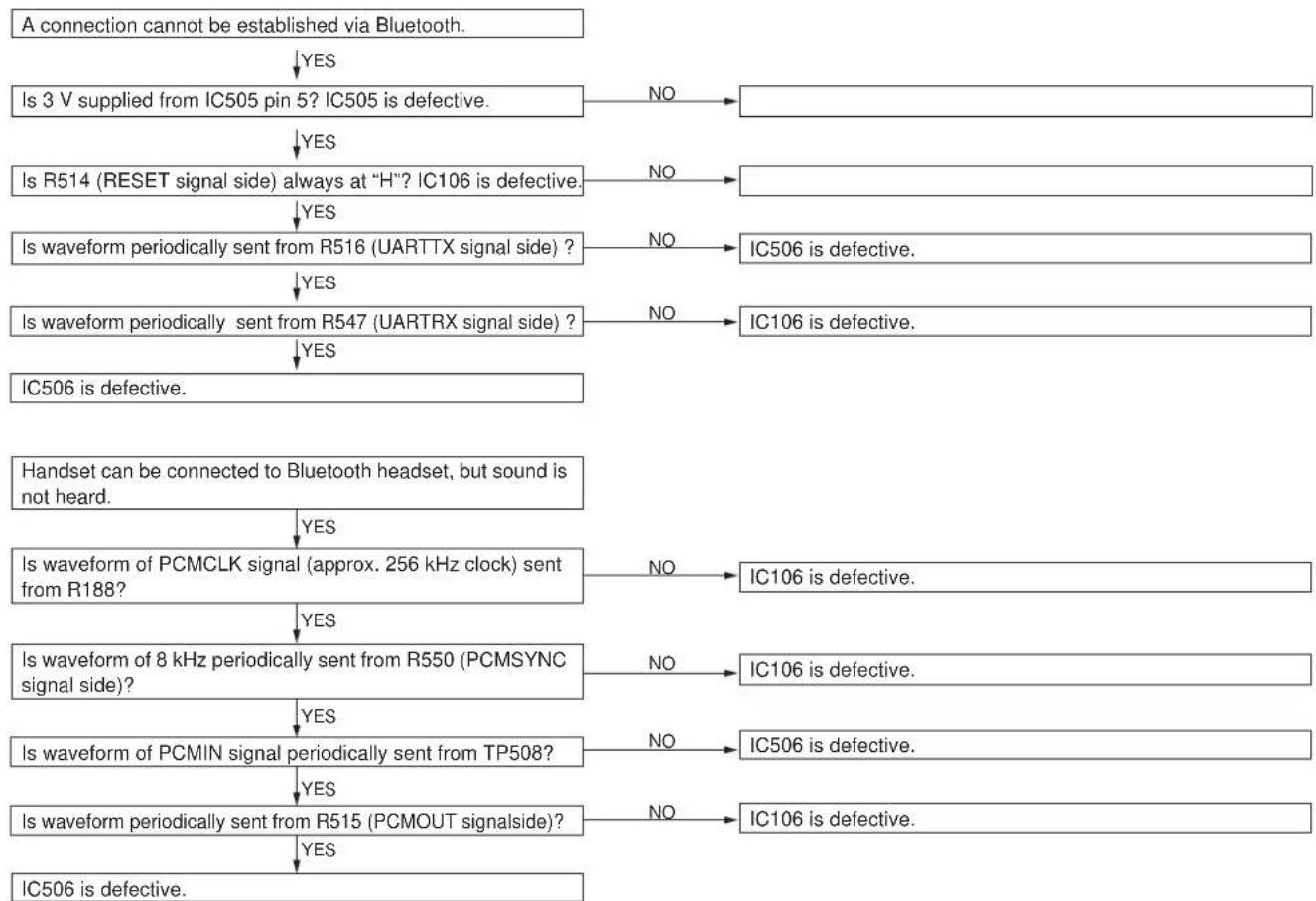
flowchart
graph TD
    A["A connection cannot be established via Bluetooth."] --> B{Is 3 V supplied from IC505 pin 5? IC505 is defective.}
    B -->|YES| C["Is R514 (RESET signal side) always at "H"? IC106 is defective."]
    B -->|NO| D["IC506 is defective."]
    C --> E{Is waveform periodically sent from R516 (UARTTX signal side) ?}
    E -->|YES| F["Is waveform periodically sent from R547 (UARTRX signal side) ?"]
    E -->|NO| G["IC106 is defective."]
    C -->|YES| H{IC506 is defective.}
    H --> I["Handset can be connected to Bluetooth headset, but sound is not heard."]
    I --> J{Is waveform of PCMCLK signal (approx. 256 kHz clock) sent from R188?}
    J -->|YES| K{Is waveform of 8 kHz periodically sent from R550 (PCMSYNC signal side)?}
    K -->|NO| L["IC106 is defective."]
    K -->|YES| M{Is waveform of PCMIN signal periodically sent from TP508?}
    M -->|YES| N{Is waveform periodically sent from R515 (PCMOUT signalside)?}
    N -->|NO| O["IC106 is defective."]
    N -->|YES| P{IC506 is defective.}
CONFIDENTIAL
CHAPTER 3. DISASSEMBLY AND REASSEMBLY
A. BATTERY REMOVAL
1) Remove the battery cover.

natural_image
Illustration of a hand inserting a card into a device (no text or symbols visible)2) Remove the battery.
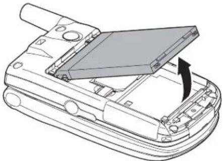
natural_image
Line drawing of a mobile phone casing with an open lid and internal components (no text or symbols)B. SPEAKER REMOVAL
1) Open the display section. Remove the screw cover, and remove the special screw.
* When removing the special screw, use the exclusive tool.
* When tightening the screws, follow the tightening sequence of (a), (b), (c), and (d).

text_image
Diagram showing exploded view of a mobile phone's internal components with labeled parts and an arrow indicating assembly direction.3) Remove the speaker from the cabinet B unit.
* When installing the speaker, fit the speaker projection (a) with the concaved rib section.
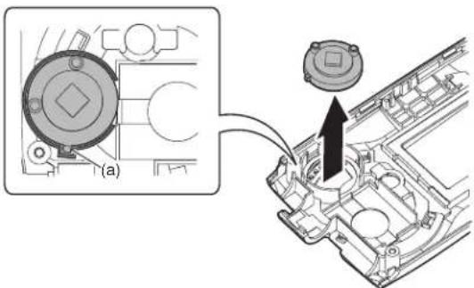
text_image
(a)C. VIBRATING MOTOR REMOVAL
1) Open the display section. Remove the screw cover, and remove the special screw.
* When removing or installing the special screw, use the exclusive tool.
* When tightening the screws, follow the tightening sequence of (a), (b), (c), and (d).

2) Disengage the pawls, and cabinet D unit. Remove the side key, the jack cover, and the external connector cover.
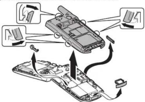
text_image
Diagram illustrating the internal components of a device, showing battery, circuit board, and cable connections with directional arrows.3) Remove the vibrating motor from the cabinet D unit.

natural_image
Technical diagram of a mechanical assembly with an upward arrow indicating a component (no text or symbols present)CONFIDENTIAL
D. BACKUP BATTERY REMOVAL
1) Remove the backup battery from the main/LCD PWB unit.
* When installing the battery, be careful of the installing direction and install it diagonally from the lower side of the battery holder spring.

text_image
Diagram showing a device with a plus button and an arrow indicating direction, alongside a magnified view of a mechanical component.E. MAIN/LCD PWB UNIT REMOVAL
1) Remove the ANT dust-proof sheet (a) and the submersion sheet (b), and remove the main/LCD PWB unit (c).

text_image
(a) (b) (c)* When attaching the ANT dust-proof sheet (a), fit it with the RF external antenna connector with the main/LCD PWB silk section as the reference.
* When attaching the submersion sheet (b), attach it inside the bump area.

natural_image
Technical diagram showing two views of a mechanical assembly with labeled components (a) and (b), no readable text or symbols present.* When attaching the PWB unit, rotate the main PWB and the LCD PWB 180 degrees in the arrow direction to wind the flat cable.

natural_image
3D diagram of a mechanical assembly with two components connected by a pipe, showing internal components and motion arrows (no text or symbols)2) Remove the camera shield case unit from the main/LCD PWB unit, and remove the camera flexible unit. Disengage the pawl, and remove the sub LCD unit. Disconnect the connector.

text_image
Diagram illustrating a mechanical assembly with labeled components and directional arrows indicating motion or flow.3) Remove the connector (a). Disengage the pawl, and remove the main/LCD unit. Disconnect the connector (b).
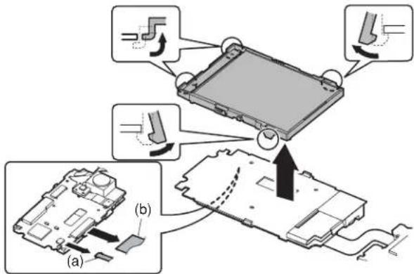
text_image
Technical diagram showing mechanical assembly steps with labeled components (a), (b), and directional arrows indicating motion or movement.F. SUB LCD REMOVAL
1) Remove the sub LCD from the sub LCD holder unit.
* Hold the both ends of the sub LCD as shown in the figure, and never press TAB (a).
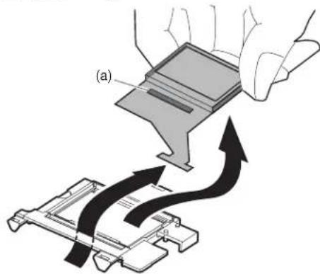
text_image
(a)CONFIDENTIAL
G. MAIN LCD, BL FLEXIBLE UNIT REMOVAL
1) Remove the main LCD from the main LCD holder unit. Remove the BL flexible unit.
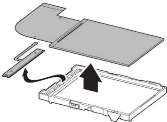
natural_image
Diagram of a device's internal structure showing a tray, casing, and housing with an arrow indicating motion (no text or symbols present)* Hold the both ends of the main LCD as shown in the figure, and never press TAB (a).

natural_image
Illustration of a hand holding a rectangular electronic component labeled (a), with no visible text or symbols on the diagram itself.H. RECEIVER AND MIC REMOVAL
1) Remove the receiver and the mic from the cabinet A/C unit.
* When attaching the receiver, be sure to face the terminal (a) tip toward the inside without covering over the rib.
* When handling the mic, use a pair of tweezers to hold the peripheral of the mic, and be careful not to touch the front and the rear of the mic.

natural_image
Technical diagram showing two views of a device's internal structure, one with an attached component and the other with a handle (no text or symbols present)* When attaching the mic, be sure to set the spring direction vertically to the cabinet.

natural_image
Technical line drawing of a mechanical component with no visible text or symbolsTM200 DISASSEMBLY AND REASSEMBLY
CHAPTER 4. DIAGRAMS
[1] Block diagram
[Main]
CONFIDENTIAL
CONFIDENTIAL

flowchart
graph TD
    subgraph Top-Left
        A["RF I/F (BRIGHTSE)"] --> B["ADC8535 (Typhoon)"]
        B --> C["ADC8539 (Hearner)"]
        C --> D["ADC8539 (Hearner)"]
        D --> E["ADC8539 (Hearner)"]
    end

    subgraph Top-Right
        F["Bluetooth module (UQN2+D01A)"] --> G["Auto Focus"]
        G --> H["CDD Sensor"]
        H --> I["V-Driver"]
        I --> J["BD6020 + BD6033"]
        J --> K["LCD Controller (UR38462)"]
        K --> L["GDS module"]
        L --> M["LTC205"]
        M --> N["LCD Bandpass"]
        N --> O["Speaker"]
    end

    subgraph Bottom-Left
        P["ADC8539 (Hearner)"] --> Q["ADC8539 (Hearner)"]
        Q --> R["ADC8539 (Hearner)"]
        R --> S["ADC8539 (Hearner)"]
    end

    subgraph Bottom-Right
        T["ADC8539 (Hearner)"] --> U["ADC8539 (Hearner)"]
        U --> V["ADC8539 (Hearner)"]
    end

    A --> W["RF I/F (BRIGHTSE)"]
    C --> X["ADC8539 (Hearner)"]
    D --> Y["ADC8539 (Hearner)"]
    E --> Z["ADC8539 (Hearner)"]
    F --> AA["ADC8539 (Hearner)"]
    G --> AB["ADC8539 (Hearner)"]
    H --> AC["ADC8539 (Hearner)"]
    I --> AD["ADC8539 (Hearner)"]
    J --> AE["ADC8539 (Hearner)"]
    K --> AF["ADC8539 (Hearner)"]
    L --> AG["ADC8539 (Hearner)"]
    M --> AH["ADC8539 (Hearner)"]
    N --> AI["ADC8539 (Hearner)"]
    O --> AJ["ADC8539 (Hearner)"]
    P --> AK["ADC8539 (Hearner)"]
    Q --> AL["ADC8539 (Hearner)"]
    R --> AM["ADC8539 (Hearner)"]
    S --> AN["ADC8539 (Hearner)"]
    T --> AO["ADC8539 (Hearner)"]
    U --> AP["ADC8539 (Hearner)"]
    V --> AQ["ADC8539 (Hearner)"]
    W --> AR["ADC8539 (Hearner)"]
    X --> AS["ADC8539 (Hearner)"]
    Y --> AT["ADC8539 (Hearner)"]
    Z --> AU["ADC8539 (Hearner)"]
    AA --> AV["ADC8539 (Hearner)"]
    AB --> AW["ADC8539 (Hearner)"]
    AC --> AX["ADC8539 (Hearner)"]
    AD --> AY["ADC8539 (Hearner)"]
    AE --> AZ["ADC8539 (Hearner)"]
    AF --> BA["ADC8539 (Hearner)"]
    AG --> BB["ADC8539 (Hearner)"]
    AH --> BC["ADC8539 (Hearner)"]
    AI --> BD["ADC8539 (Hearner)"]
    AJ --> BE["ADC8539 (Hearner)"]
    AK --> BF["ADC8539 (Hearner)"]
    AL --> BG["ADC8539 (Hearner)"]
    AM --> BH["ADC8539 (Hearner)"]
    AN --> BI["ADC8539 (Hearner)"]
    AO --> BJ["ADC8539 (Hearner)"]
    AP --> BK["ADC8539 (Hearner)"]
    AQ --> BL["ADC8539 (Hearner)"]
    AR --> BM["ADC8539 (Hearner)"]
    AS --> BN["ADC8539 (Hearner)"]
    AT --> BO["ADC8539 (Hearner)"]
    AU --> BP["ADC8539 (Hearner)"]
    AV --> BQ["ADC8539 (Hearner)"]
    AW --> BR["ADC8539 (Hearner)"]
    AX --> BS["ADC8539 (Hearner)"]
    AZ --> BT["ADC8539 (Hearner)"]
    BA --> BU["ADC8539 (Hearner)"]
    BW --> BV["ADC8539 (Hearner)"]

    subgraph Bottom-Left
        C
        D
        E
        F
        G
        H
        I
        J
        K
        L
        M
        N
        O
        P
        Q
        R
        S
        T
        U
        V
        W
        X
        Y
        Z
        AA
        AB
        AC
        AD
        AE
        AF
        AG
        AH
        AI
        AJ
        AK
        AL
        AM
        AN
        AO
        AP
        AQ
        AR
        AS
        AT
        AU
        AV
        AW
        AX
        AX
        BY
        BY
        CA
        CA
        DB
        DB
        DB
        DB
        DB
        DB
        DB
        DB
        DB
        DB
        DB
        DB
        DB
        DB
        DB
        DB
        DB
        DB
        DB
        DB
        DB
        DB
        DB
        DB
        DB
        DB
        DB
        DB
        DB
        DB
        DB
        DB
        DB
        DB

    subgraph Bottom-Right
        C
        D
        E
        F
        G
        H
        I
        J
        K
        L
        M
        N
        O
        P
        Q
        R
        S
        T
        U
        V
        W
        X
        Y
        Z
        AA
        AB
        AC
        AD
        AE
        AF
        AG
        AH
        AI, AJ, AK, AL, AM, AN, AO, AP, OB, OR, OP, AP, OP, OP, OP, OP, OP, OP, OP, OP, OP, OP, OP, OP, OP, OP, OP, OP, OP, OP, OP, OP, OP, OP, OP, OP, OP, OP, OP, OP, OP, OP, OP, OP, OP, OP, OP, OP, OP, OP, OP, OP, OP, OP, OP, OP, OP, OP, OP, OP, OP, OP, UP

    subgraph Bottom-Left |
| AC & AC Components: 4.1 - 4.2

    A1["Accresive Connector 400V7C100-600V600"] --> B1["BASELIC Components"]
    A2["BASELIC Components"] --> B2["BASELIC Components"]
    A3["BASELIC Components"] --> B3["BASELIC Components"]
    A4["BASELIC Components"] --> B4["BASELIC Components"]
    A5["BASELIC Components"] --> B5["BASELIC Components"]
    A6["BASELIC Components"] --> B6["BASELIC Components"]
    A7["BASELIC Components"] --> B7["BASELIC Components"]
    A8["BASELIC Components"] --> B8["BASELIC Components"]
    A9["BASELIC Components"] --> B9["BASELIC Components"]
    A10["BASELIC Components"] --> B10["BASELIC Components"]
    A11["BASELIC Components"] --> B11["BASELIC Components"]
    A12["BASELIC Components"] --> B12["BASELIC Components"]
    A13["BASELIC Components"] --> B13["BASELIC Components"]
    A14["BASELIC Components"] --> B14["BASELIC Components"]
    A15["BASELIC Components"] --> B15["BASELIC Components"]
    A16["BASELIC Components"] --> B16["BASELIC Components"]
    A17["BASELIC Components"] --> B17["BASELIC Components"]
    A18["BASELIC Components"] --> B18["BASELIC Components"]
    A19["BASELIC Components"] --> B19["BASELIC Components"]
    A20["BASELIC Components"] --> B20["BASELIC Components"]
    A21["BASELIC Components"] --> B21["BASELIC Components"]
    A22["BASELIC Components"] --> B22["BASELIC Components"]
    A23["BASELIC Components"] --> B23["BASELIC Components"]
    A24["BASELIC Components"] --> B24["BASELIC Components"]
    A25["BASELIC Components"] --> B25["BASELIC Components"]
    A26["BASELIC Components"] --> B26["BASELIC Components"]
    A27["BASELIC Components"] --> B27["BASELIC Components"]
    A28["BASELIC Components"] --> B28["BASELIC Components"]
    A29["BASELIC Components"] --> B29["BASELIC Components"]
    A30["BASELIC Components"] --> B30["BASELIC Components"]
    A31["BASELIC Components"] --> B31["BASELIC Components"]
    A32["BASELIC Components"] --> B32["BASELIC Components"]
    A33["BASELIC Components"] --> B33["BASELIC Components"]
    A34["BASELIC Components"] --> B34["BASELIC Components"]
    A35["BASELIC Components"] --> B35["BASELIC Components"]
    A36["BASELIC Components"] --> B36["BASELIC Components"]
    A37["BASELIC Components"] --> B37["BASELIC Components"]
    A38["BASELIC Components"] --> B38["BASELIC Components"]
    A39["BASELIC Components"] --> B39["BASELIC Components"]
    A40["BASELIC Components"] --> B40["BASELIC Components"]
    A41["BASELIC Components"] --> B41["BASELIC Components"]
    A42["BASELIC Components"] --> B42["BASELIC Components"]
    A43["BASELIC Components"] --> B43["BASELIC Components"]
    A44["BASELIC Components"] --> B44["BASELIC Components"]
    A45["BASELIC Components"] --> B45["BASELIC Components"]
    A46["BASELIC Components"] --> B46["BASELIC Components"]
    A47["BASELIC Components"] --> B47["BASELIC Components"]
    A48["BASELIC Components"] --> B48["BASELIC Components"]
    A49["BASELIC Components"] --> B49["BASELIC Components"]
    A50["BASELIC Components"] --> B50["BASELIC Components"]
    A51["BASELIC Components"] --> B51["BASELIC Components"]
    A52["BASELIC Components"] --> B52["BASELIC Components"]
    A53["BASELIC Components"] --> B53["BASELIC Components"]
    A54["BASELIC Components"] --> B54["BASELIC Components"]
    A55["BASELIC Components"] --> B55["BASELIC Components"]
    A56["BASELIC Components"] --> B56["BASELIC Components"]
    A57["BASELIC Components"] --> B57["BASELIC Components"]
    A58["BASELIC Components"] --> B58["BASELIC Components"]
    A59["BASELIC Components"] --> B59["BASELIC Components"]
    A60["BASELIC Components"] --> B60["BASELIC Components"]
    A61["BASELIC Components"] --> B61["BASELIC Components"]
    A62["BASELIC Components"] --> B62["BASELIC Components"]
    A63["BASELIC Components"] --> B63["BASELIC Components"]
    A64["BASELIC Components"] --> B64["BASELIC Components"]
    A65["BASELIC Components"] --> B65["BASELIC Components"]

    subgraph Bottom-Left Side Bus / GPIO INT

    C1[COMON Power 1kW 1kW 1kW 1kW 1kW 1kW 1kW 1kW 1kW 1kW 1kW 1kW 1kW 1kW 1kW 1kW 1kW 1kW 1kW 1kW 1kW 1kW 1kW 1kW 1kW 1kM 1kM 1kM 1kM 1kM 1kM 1kM 1kM 1kM 1kM 1kM 1kM 1kM 1kM 1kM 1kM 1kM 1kM 1kM 1kM 1kM 1kM 1kM 1kM 1kM 1k M 1kM 1kM 1kM 1kM 1kM 1kM 1kM 1kM 1kM 1kM 1kM 1kM 1kM 1kM 1kM 1kM 1kM 1kM 1kM 1kM 1kM 1kM 1kM 1kM 1kCm 1kCm 1kCm 1kCm 1kCm 1kCm 1kCm 1kCm 1kCm 1kCm 1kCm 1kCm 1kCm 1kCm 1kCm 1kCm 1kCm 1kCm 1kCm 1kCm 1kC m 1kCm 1kCm 1kCm 1kCm 1kCm 1kCm 1kCm 1kCm 1kCm 1kCm 1kCm 1kCm 1kCm 1kCm 1kCm 1kCm 1kCm 1kCm 1Kc m 1Kc m 1Kc m 1Kc m 1Kc m 1Kc m 1Kc m 1Kc m 1Kc m 1Kc m 1Kc m 1Kc m 1Kc m 1Kc m 1Kc m 1Kc m 1Kc m 1Kc m
[RF]
CONFIDENTIAL
CONFIDENTIAL
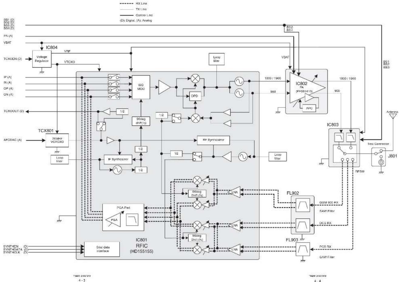
flowchart
graph TD
    subgraph Sensor_4-3
        A["SYNTHEN"] --> B["SYNTHOLK"]
        C["SYNTHDATA"] --> D["SIst data interface"]
        E["SYNTH0X"] --> F["IC801 RFIC (HD155155)"]
        G["IC802 PA (FFD081410)"] --> H["IC803"]
    end

    subgraph Sensor_4-4
        I["SYNTHEN"] --> J["FL902"]
        K["SYNTHDATA"] --> L["FL903"]
        M["SYNTH0X"] --> N["PQA Part"]
        O["SYNTH0Y"] --> P["IF Synthasizer"]
        Q["SYNTH0Z"] --> R["90deg shr(%)"]
        S["SYNTH0A"] --> T["90deg Shrl(%)"]
        U["SYNTH0C"] --> V["90deg Shrl(%)"]
        W["SYNTH0D"] --> X["90deg Shrl(%)"]
        Y["SYNTH0E"] --> Z["90deg Shrl(%)"]
        AA["SYNTH0F"] --> AB["90deg Shrl(%)"]
        AC["SYNTH0G"] --> AD["90deg Shrl(%)"]
        AE["SYNTH0H"] --> AF["90deg Shrl(%)"]
        AG["SYNTH0I"] --> AH["90deg Shrl(%)"]
        AI["SYNTH0J"] --> AJ["90deg Shrl(%)"]
        AK["SYNTH0K"] --> AL["90deg Shrl(%)"]
        AM["SYNTH0L"] --> AN["90deg Shrl(%)"]
        AO["SYNTH0M"] --> AP["90deg Shrl(%)"]
        AQ["SYNTH0N"] --> AR["90deg Shrl(%)"]
        AS["SYNTH0O"] --> AT["90deg shr(%)"]
        AU["SYNTH0P"] --> AV["90deg shrl(%)"]
        AW["SYNTH0Q"] --> AX["90deg shrl(%)"]
        AY["SYNTH0T"] --> AZ["90deg shrl(%)"]
        BA["SYNTH0U"] --> BB["90deg shrl(%)"]
        BC["SYNTH0V"] --> BD["90deg shrl(%)"]
        BE["SYNTH0W"] --> BF["90deg shrl(%)"]
        BG["SYNTH0X"] --> BH["90deg shrl(%)"]
        BI["SYNTH0Y"] --> BJ["90deg shrl(%)"]
        BK["SYNTH0Z"] --> BL["90deg shrl(%)"]
        BM["SYNTH0A"] --> BN["90deg shrl(%)"]
        BO["SYNTH0C"] --> BP["90deg shrl(%)"]
        BQ["SYNTH0Y"] --> BR["90deg shrl(%)"]
        BS1["D3"] --> BT["VBAT"]
        BS2["D3"] --> BU["VBAT"]
        BS3["D3"] --> BV["B21 B22 B23"]
    end

    subgraph Control_Link
        BI --> BA
        BJ --> BB
        BC --> BF
        BF --> BG
    end

    subgraph Wave_Liter
        BI --> BA
        BB --> BF
    end

    subgraph Loop_Liter
        BI --> BF
    end

    subgraph Filter_Liter
        BI --> BF
    end

    subgraph Test_Conector
        BI --> BJ
    end

    subgraph Antenna
        BI --> BJ
    end

    subgraph Power_Liter
        BI --> BF
    end

    subgraph Control_Link
        BI --> BF
    end

    subgraph Wave_Liter
        BI --> BF
    end

    subgraph Power_Liter
        BI --> BF
    end

    subgraph Filter_Liter
        BI --> BF
    end

    subgraph Power_Liter
        BI --> BF
    end

    subgraph Control_Link
        BI --> BF
    end

    subgraph Power_Liter
        BI --> BF
    end

    subgraph Power_Liter
        BI --> BF
    end

    subgraph Control_Link
        BI --> BF
    end

    subgraph Power_Liter
        BI --> BF
    end

    subgraph Power_Liter
        BI --> BF
    end

    subgraph Control_Link
        BI --> BF
    end

    subgraph Power_Liter
        BI --> BF
    side by side

    subgraph Power_Liter
        BI --> BF
    end

    subgraph Control_Link
        BI --> BF
    end

    subgraph Power_Liter
        BI --> BF
    end

    subgraph Control_Link
        BI --> BF
    end

    subgraph Power_Liter
        BI --> BF
    end

    subgraph Control_Link
        BI --> BF
    end

    subgraph Power_Liter
        BI --> BF
    end

    subgraph Control_Link
        BI --> BF
    end

    subgraph Power_Liter
        BQ1_BQ2_BQ3
CONFIDENTIAL
(1) Sound signal system
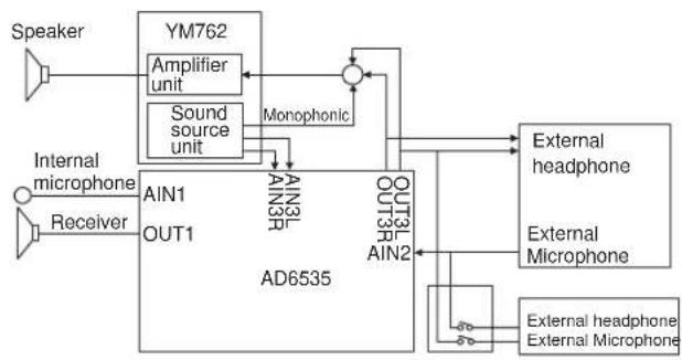
flowchart
graph TD
    A["Speaker"] --> B["AMplifier unit"]
    B --> C["Sound source unit"]
    C --> D["Monophonic"]
    D --> E["AD6535"]
    F["Internal microphone"] --> G["Receiver"]
    G --> H["AIN1 OUT1"]
    H --> I["AIN2 OUT1"]
    I --> J["OUT3L IN2"]
    J --> K["External headphone"]
    J --> L["External Microphone"]
    J --> M["External headphone"]
    J --> N["External Microphone"]
    style A fill:#f9f,stroke:#333
    style F fill:#f9f,stroke:#333
    style G fill:#f9f,stroke:#333
    style H fill:#ccf,stroke:#333
    style I fill:#ccf,stroke:#333
    style J fill:#ccf,stroke:#333
    style K fill:#dfd,stroke:#333
    style L fill:#dfd,stroke:#333
    style M fill:#dfd,stroke:#333
    style N fill:#dfd,stroke:#333
(4) Interface
flowchart
graph LR
    A["Interface SW"] --> B["BU7880"]
    C["UART"] --> B
    D["Analog"] --> B
    E["Serial"] --> B
    F["UART"] --> B
    G["USB"] --> B
    B --> H["I/F CN"]
(2) LCD & camera system

flowchart
graph TD
    A["Flash LED"] --> B["Backlight LED"]
    B --> C["LTC3205"]
    C --> D["Power sourceIC BD6020 +BD6030"]
    D --> E["-8V"]
    D --> F["+1.8V"]
    D --> G["+1.5V"]
    D --> H["+3.0V"]
    D --> I["+3.0V"]
    J["LCD"] --> K["LCD controller"]
    K --> L["I/F"]
    K --> M["+1.8V"]
    K --> N["+3.0V"]
    O["Series regulator"] --> P["+3.0V"]
    O --> Q["+1.8V"]
    R["CCD camera I/F"] --> S["+3.0V"]
(5) Vibration Motor & LED Driver
flowchart
graph TD
    M["Motor M"] --> LDO["LDO"]
    LDO --> ON/OFF["ON/OFF"]
    ON/OFF --> YM762["YM762"]
    YM762 --> AD6535["Typhoon"]
    AD6535 --> Key["Key LED-Light"]
    Key --> LDO
(3) Battery charge system

flowchart
graph TD
    A["AC charger"] --> B["Constant voltage"]
    B --> C["Constant current"]
    D["VDT"] --> E["OVP"]
    F["reg"] --> G["AD6535"]
    G --> H["Lithium ion Battery pack"]
    I["Power Supply"] --> J["Resistor"]
    K["Current Source"] --> L["Current Source"]
    M["Current Source"] --> N["Current Source"]
(6) Sense Flip
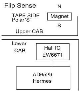
flowchart
graph TD
    A["Upper CAB"] --> B["TAPE SIDE Polar"S""]
    B --> C["Magnet"]
    C --> D["S"]
    E["Lower CAB"] --> F["Hall IC EW6671"]
    F --> G["AD6529 Hermes"]
CONFIDENTIAL
CHAPTER 5. SCHEMATIC DIAGRAM AND WIRING SIDE OF P.W.BOARD
[1] NOTES ON SCHEMATIC DIAGRAM
- Resistor:
To differentiate the units of resistors, the symbols K and M are used. The symbol K means 1000 ohm and the symbol M means 1000 kohm. The resistor without any symbol is an ohm resistor.
- Capacitor:
To indicate the unit of capacitor, the symbol is used.
The symbol P means pico-farad and the unit of the capacitor without such a symbol is microfarad. As to electrolytic capacitor, the expression “capacitance/withstand voltage” is used.
(CH), (RH), (UJ): Temperature compensation
(ML) : Mylar type
(S) : Styrol type
(PP) : Polypropylene type
- The indicated voltage in each section is the one measured by Digital Multimeter between such a section and the chassis with no signal given.
- Conditions: SIM card inserted, power on, in stand-by mode (opened)
- Schematic diagram and Wiring Side of P.W. Board for this model are subject to change for improvement without prior notice.
- Parts marked with “⚠️” are important for maintaining the safety of the set. Be sure to replace these parts with specified ones for maintaining the safety and performance of the set.
[2] TYPES OF TRANSISTOR AND LED
![SHARP TM200 - [2] TYPES OF TRANSISTOR AND LED - 1](/content/2026/06/1212016/images/27f6db1f8ddfc68dd24303dc994279943758323b72c56528a4eb4d4f05aa820a.jpg)
text_image
B (3) (G) E (1) (S) TOP VIEW C (2) (D)2SK3019 RT1N144 U
![SHARP TM200 - [2] TYPES OF TRANSISTOR AND LED - 2](/content/2026/06/1212016/images/8ba7ef0ea6b9412a97d0008340af1087df72b3aaa6fdc64a0f8efd6e5cce5fc0.jpg)
CPH6311
![SHARP TM200 - [2] TYPES OF TRANSISTOR AND LED - 3](/content/2026/06/1212016/images/9616c2ef3b1a7023f16dffbccbbeedb7dcbdb5295a65980e7259c72b9938071a.jpg)
text_image
① S1 G1 S2 G2 ④ TOP VIEW ⑧ D1 D1 D2 D2 ⑤ECH8603
![SHARP TM200 - [2] TYPES OF TRANSISTOR AND LED - 4](/content/2026/06/1212016/images/e5b0a58c43b8dedcba6fe259533df38b48dafe481048159d3ff20bdd48c3368d.jpg)
text_image
1 (D) 2 (D) 3 (G) TOP VIEW 6 (D) 5 (D) 4 (S)MCH6413
![SHARP TM200 - [2] TYPES OF TRANSISTOR AND LED - 5](/content/2026/06/1212016/images/29e1f2b24390f9ab98536b2db72a99ab443a9837ee77b66985872a79f27524c9.jpg)
EC4301 C
EC4401 C
TOP VIEW
![SHARP TM200 - [2] TYPES OF TRANSISTOR AND LED - 6](/content/2026/06/1212016/images/59804175c18c2e02ca064c3abefd92ec6e34b9a71cf39c2160125427548dddd1.jpg)
1SS388
1SS405
RB160M30
RB521S30
RB551V30
RB520S30
TOP VIEW
![SHARP TM200 - [2] TYPES OF TRANSISTOR AND LED - 7](/content/2026/06/1212016/images/13b288464e8bc5112ef3f29c5db6efece383bee04d684d56f73eef15cdd460d8.jpg)
HN2S01FU
TOP VIEW
![SHARP TM200 - [2] TYPES OF TRANSISTOR AND LED - 8](/content/2026/06/1212016/images/b6bcbd50b8c52e77d246a2e3727c3988dd712b37f2cf8710191e782b4f620679.jpg)
TOP VIEW
![SHARP TM200 - [2] TYPES OF TRANSISTOR AND LED - 9](/content/2026/06/1212016/images/8a0e05d3193c7b0e4fb772b94087bc58f05fc48cb9aa18c7bd30f4f4c039db98.jpg)
RSB6.8S
TOP VIEW
![SHARP TM200 - [2] TYPES OF TRANSISTOR AND LED - 10](/content/2026/06/1212016/images/f0622fab4b8923398efa863361c2cb166cd42d4f669273c7ac34ca0a1340db74.jpg)
YPY1105C
FR1105C
GM1BC35370AC
TOP VIEW TOP VIEW
![SHARP TM200 - [2] TYPES OF TRANSISTOR AND LED - 11](/content/2026/06/1212016/images/9c29775c8c1ccf23325a2671a3e8dccc6cf84e74ce72c4a1edf9cdd27929490a.jpg)
NECW008A
![SHARP TM200 - [2] TYPES OF TRANSISTOR AND LED - 12](/content/2026/06/1212016/images/5e743440cffa5ffd81b2850c7584f774fc46061928b85c6878a06dd3dc712cb0.jpg)
CONFIDENTIAL
[3] WAVEFORMS OF CIRCUIT

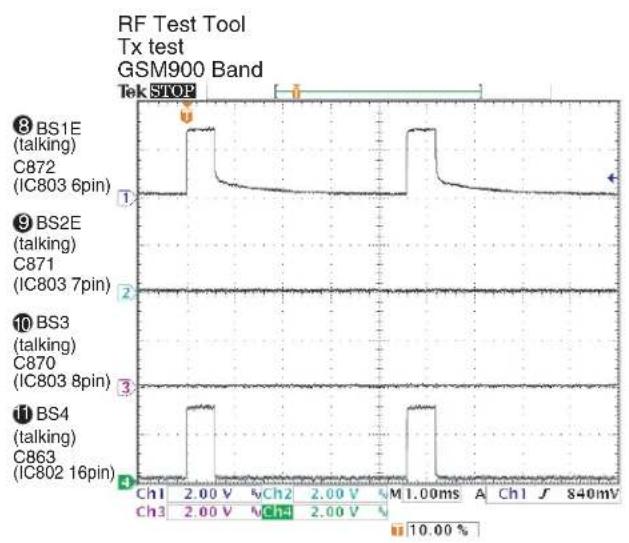
line
| Channel | Label | Value | |---------|-----------------|-----------| | BS1E | (talking) | 8.00 V | | BS2E | (talking) | 9.00 V | | BS3 | (talking) | 10.00 V | | BS4 | (talking) | 11.00 V | | C872 | (IC803 6pin) | 1.00 ms | | C871 | (IC803 7pin) | 2.00 V | | C870 | (IC803 8pin) | 3.00 V | | C863 | (IC802 16pin) | 4.00 ms |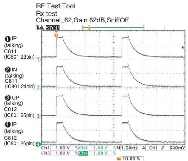
line
| Component | Channel | Voltage (V) | |-----------|---------|-------------| | IP | C811 | 23pin | | IN | C811 | 24pin | | QP | C812 | 25pin | | IP | C812 | 26pin |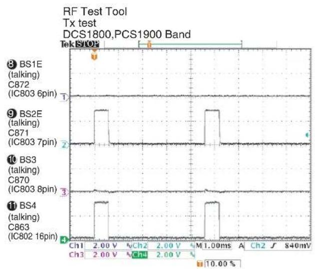
line
| Channel | Pulse Label | Voltage (V) | |---------|-------------|-------------| | BS1E | (talking) | 803 6 | | BS2E | (talking) | 7 | | BS3 | (talking) | 8 | | BS4 | (talking) | 16 |
line
| Channel | Pin Label | Value | | ------------- | ----------------- | --------- | | SYNTHEN | Stand-by | 29pin | | SYNTHCLK | Stand-by | 30pin | | SYNTHDATA | Stand-by | 32pin |TM200 CIRCUIT DIAGRAM AND PWB LAYOUT
CONFIDENTIAL

line
| Signal | Label | Value | |--------|-----------------|-----------| | BS1E | (talking) | 8.00 V | | BS2E | (talking) | 9.00 V | | BS3 | (talking) | 10.00 V | | BS4 | (talking) | 11.00 V | | C872 | (IC803 6pin) | 2.00 V | | C871 | (IC803 7pin) | 2.00 V | | C870 | (IC803 8pin) | 2.00 V | | C863 | (IC802 16pin) | 2.00 V |12 13MHz IN (Point R261) To Digital Base Band LSI Pin142

line
| Time (ms) | Amplitude | | --------- | --------- | | 0 | 0 | | 500 | -33 | | 1000 | 0 | | 1500 | -33 | | 2000 | 0 | | 2500 | -33 | | 3000 | 0 | | 3500 | -33 | | 4000 | 0 | | 4500 | -33 | | 5000 | 0 | | 5500 | -33 | | 6000 | 0 | | 6500 | -33 | | 7000 | 0 |
line
| Signal | Channel | Voltage (V) | Current (pin) | |--------|---------|-------------|---------------| | BS1E | C872 | 2.00 | 6 | | BS2E | C871 | 2.00 | 7 | | BS3 | C870 | 2.00 | 8 | | BS4 | C863 | 2.00 | 16 |13 13MHz OUT (Point R166) from Digital Base Band LSI Pin84
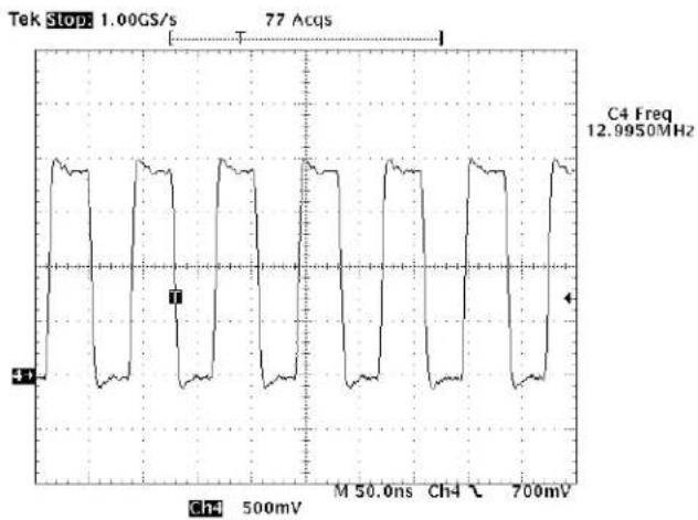
line
| Time (ms) | Voltage (mV) | | --------- | ------------ | | 0 | 0 | | 500 | 0 | | 1000 | 0 | | 1500 | 0 | | 2000 | 0 | | 2500 | 0 | | 3000 | 0 | | 3500 | 0 | | 4000 | 0 | | 4500 | 0 | | 5000 | 0 | | 5500 | 0 | | 6000 | 0 | | 6500 | 0 | | 7000 | 0 | | 7500 | 0 |14 32.768KHz IN (Point-R152) To Digital Base Band LSI Pin49

line
| Time (μs) | Voltage (mV) | | --------- | ------------ | | 0 | -124 | | 200 | 200 | | 10.0 | 10.0 | | 24 | 24 |CONFIDENTIAL
⑮ DCLK (Point-R759 on LCDC_PCB) To LCD Unit pin26

line
| Time (ms) | Voltage (mV) | | --------- | ------------ | | 0 | 0 | | 1.00 | 0 | | 2.00 | 0 | | 3.00 | 0 | | 4.00 | 0 | | 5.00 | 0 | | 6.00 | 0 | | 7.00 | 0 | | 8.00 | 0 | | 9.00 | 0 | | 10.00 | 0 | | 11.00 | 0 | | 12.00 | 0 | | 13.00 | 0 | | 14.00 | 0 | | 15.00 | 0 | | 16.00 | 0 | | 17.00 | 0 | | 18.00 | 0 | | 19.00 | 0 | | 20.00 | 0 | | 21.00 | 0 | | 22.00 | 0 | | 23.00 | 0 | | 24.00 | 0 | | 25.00 | 0 | | 26.00 | 0 | | 27.00 | 0 | | 28.00 | 0 | | 29.00 | 0 | | 30.00 | 0 | | 31.00 | 0 | | 32.00 | 0 | | 33.00 | 0 | | 34.00 | 0 | | 35.00 | 0 | | 36.00 | 0 | | 37.00 | 0 | | 38.00 | 0 | | 39.00 | 0 | | 40.00 | 0 | | 41.00 | 0 | | 42.00 | 0 | | 43.00 | 0 | | 44.00 | 0 | | 45.00 | 0 | | 46.00 | 0 | | 47.00 | 0 | | 48.01 | 5 | | 49.01 | - | | 50.97 | - | | Peak | - |16 VSYNC (Point-C760 on LCDC_PCB) To LCD Unit pin28

line
| Time (ms) | Voltage (V) | | --------- | ----------- | | 0.2 | 139 Acqs | | 1.98 | 139 Acqs |⑰ TCXOEN (Point-IC804 pin 1) From Analog Base Band LSI Pin 2

line
| Time (ms) | Amplitude (A) | | --------- | ------------- | | 0.00 | 0 | | 0.25 | 0 | | 0.50 | 1 | | 0.75 | 3 | | 1.00 | 4 | | 1.25 | 1 | | 1.50 | 0 | | 1.75 | 1 | | 2.00 | 3 | | 2.25 | 1 | | 2.50 | 0 | | 2.75 | 0 | | 3.00 | 0 | | 3.25 | 0 | | 3.50 | 0 | | 3.75 | 0 | | 4.00 | 0 | | 4.25 | 0 | | 4.50 | 0 | | 4.75 | 0 | | 5.00 | 0 | | 5.25 | 0 | | 5.50 | 0 | | 5.75 | 0 | | 6.00 | 0 | | 6.25 | 0 | | 6.50 | 0 | | 6.75 | 0 | | 7.00 | 0 | | 7.25 | 0 | | 7.50 | 0 | | 7.75 | 0 | | 8.00 | 0 | | 8.25 | 0 | | 8.50 | 0 | | 8.75 | 0 | | 9.00 | 0 | | 9.25 | 0 | | 9.50 | 0 | | 9.75 | 0 | | 10.00 | 0 |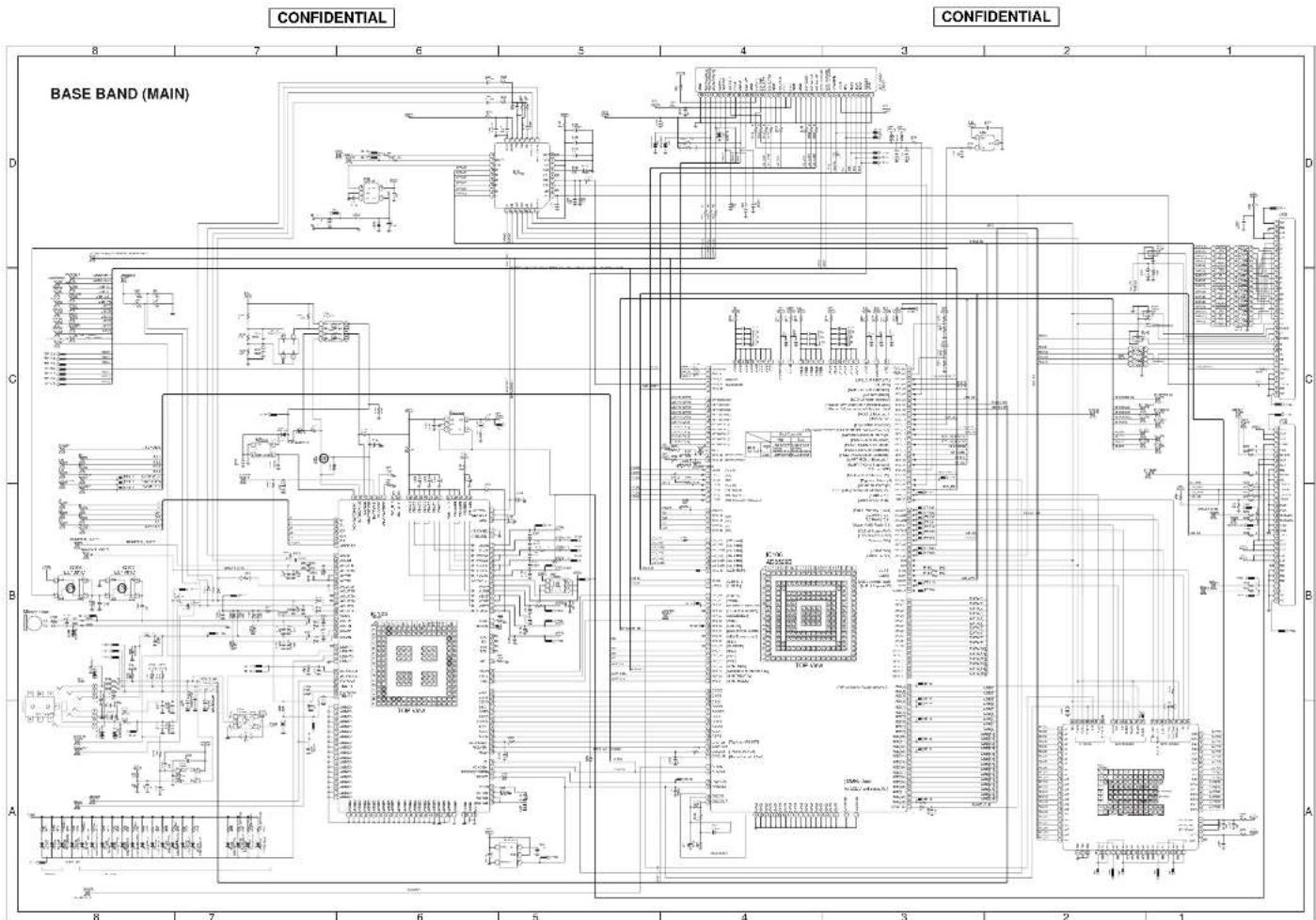
text_image
CONFIDENTIAL CONFIDENTIAL BASE BAND (MAIN) A B C D 8 7 6 5 4 3 2 1 8 7 6 5 4 3 2 1 8 7 6 5 4 3 2 1 8 7 6 5 4 3 2 1 8 7 6 5 4 3 2 1 8 7 6 5 4 3 2 1 8 7 6 5 4 3 2 1 8 8 7 6 5 4 3 2 1 8 8 7 6 5 4 3 2 1 8 8 7 6 5 4 3 2 1 8 8 7 6 5 4 3 2 1 8 8 7 6 5 4 3 2 1 8 8 7 6 5 4.5 8.5 9.0 9.5 10.0 10.5 11.0 11.5 12.0 12.5 13.0 13.5 14.0 14.5 15.0 15.5 16.0 16.5 17.0 17.5 18.0 18.5 19.0 19.5 20.0 20.5 21.0 21.5 22.0 22.5 23.0 23.5 24.0 24.5 25.0 25.5 26.0 26.5 27.0 27.5 28.0 28.5 29.0 29.5 30.0 30.5 31.0 31.5 32.0 32.5 33.0 33.5 34.0 34.5 35.0 35.5 36.0 36.5 37.0 37.5 38.0 38.5 39.0 39.5 40.0 40.5 41.0 41.5 42.0 42.5 43.0 43.5 44.0 44.5 45.0 45.5 46.0 46.5 47.0 47.5 48.0 48.5 49.0 49.5 50.0THE 2001 CIRCUIT EUROPAH AND TWO LAYOUT
THE 2005 CIRCUIT DIAGRAM AND THE LAYOUT
CONFIDENTIAL
CONFIDENTIAL
12345678
RF PART (MAIN)

text_image
Electrical schematic diagram with labeled components, wires, and measurement instrumentsCONFIDENTIAL
CONFIDENTIAL
12345678
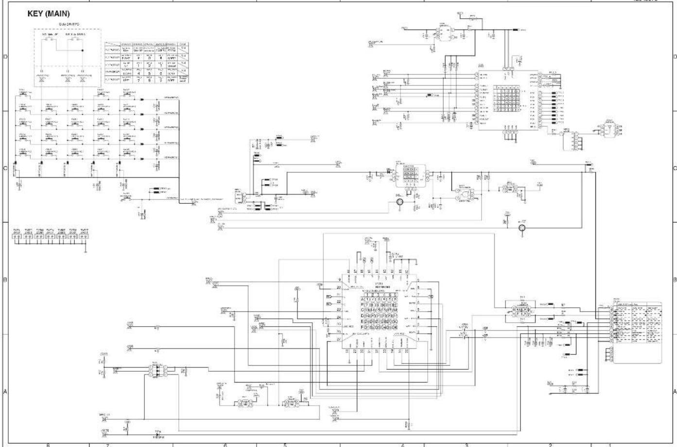
text_image
KEY (MAIN) D C B ATHE CIRCUIT DIAGNAT AND THE LAYOUT
5-9
THE 2005 CIRCUIT DIAGRAM AND THE LAYOUT
5 - 10
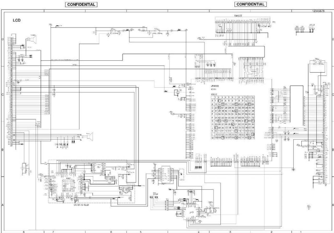
text_image
CONFIDENTIAL 12345678 LCD Sub LCD LF30863 IC 750 DC 12 A 1 2 3 4 5 6 7 8 9 10 11 12 B 13 14 15 16 17 18 19 20 21 22 23 24 C 25 26 27 28 29 30 31 32 33 34 35 36 D 37 38 39 40 41 42 43 44 45 46 47 48 F 53 54 55 56 57 58 59 60 G 61 62 63 64 65 66 67 68 69 70 71 72 H 73 74 75 76 77 78 79 80 81 82 83 I 85 86 87 88 89 90 91 92 93 94 95 96 J 98 99 100 101 102 103 104 105 106 K 107 108 109 110 111 112 L 123 124 125 126 127 M ISSN144 DC DC SHIELDTV800 D RCUIT DIAGRAM AND FWD LAYOUT
TS200 3 FOUNT DIAGRAM AND TWO LAYOUT
CONFIDENTIAL

text_image
CN502 CN104 IC103 IC106 IC101 IC801 IC902 CN501 IC506 AN501 CN102 CN502 TJX801 TCX801 IC801 IC506 CN502 TJX801 IC801 IC506 CN502 TJX801 IC801 IC506 CN502 TJX801 IC801 IC506 CN502 TJX801 IC801 IC506 CN502 TJX801 IC801 IC302 IC506 CN502 TJX801 IC801 IC506 CN502 TJX801 IC801 IC506 CN502 TJX801 IC801 IC506 CN502 TJX801 IC801 IC506 CN502 TNX801 TPX801 TPX801 TPX801 TPX801 TPX801 TPX801 TPX801 TPX801 TPX801 TPX801 TPX801 TPX801 TPX801 TPX801 TPX801 TPX801 TPX802 TPX802 TPX802 TPX802 TPX802 TPX802 TPX802 TPX802 TPX802 TPX802 TPX802 TPX802 TPX802 TPX802 TPX802 TPX802 TPX802 TPX79999999999999999999999999999999999999999999999999999999999999999999999999999999999999999999999999999 7A7555555555555555555555555555555555555555555555555555555555555555555555555 7A76333333333333333333333333333333333333333333333333333333333333333333333333333333333333333TM200 CIRCUIT DIAGRAM AND PWB LAYOUT
CONFIDENTIAL
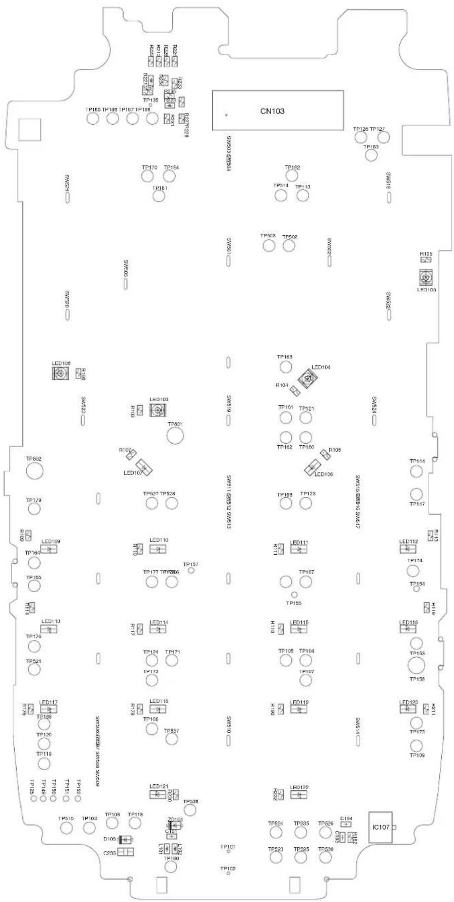
text_image
IC107 IC107 SNAMS 0.05/0.05/0.05/0.05/0.05/0.05/0.05/0.05/0.05/0.05/0.05/0.05/0.05/0.05/0.05/0.05/0.05/0.05/0.05/0.05/0.05/ CN103 SNAMS 0.05/0.05/0.05/0.05/0.05/0.05/0.05/0.05/0.05/0.05/0.05/0.05/0.05/0.05/0.05/0.05/0.05/0.05/0.05/6 SNAMS 1.1/1.1/1.1/1.1/1.1/1.1/1.1/1.1/1.1/1.1/1.1/1.1/1.1/1.1/1.1/1.1/1.1/1.1/1.1/1.1/1.1/1.1/1.1/1.1/1.1/1.1 SNAMS 2.2/2.2/2.2/2.2/2.2/2.2/2.2/2.2/2.2/2.2/2.2/2.2/2.2/2. SNAMS 3.4/4.4/4.4/4.4/4.4/4.4/4.4/4.4/4.4/4.4/4. SNAMS 4.6/6.6/6.6/6.6/6.6/6.6/6. SNAMS 5.8/8 SNAMS 7 SNAMS 9 SNAMS 11 SNAMS 13 SNAMS 15 SNAMS 17 SNAMS 19 SNAMS 21 SNAMS 23 SNAMS 25 SNAMS 27 SNAMS 29 SNAMS 31 SNAMS 33 SNAMS 35 SNAMS 37 SNAMS 39 SNAMS 41 SNAMS 43 SNAMS 45 SNAMS 47 SNAMS 49 SNAMS 51 SNAMS 53 SNAMS 55 SNAMS 57 SNAMS 59 SNAMS 61 SNAMS 63 SNAMS 65 SNAMS 67 SNAMS 69 SNAMS 71 SNAMS 73 SNAMS 75 SNAMS 77 SNAMS 79 SNAMS 81 SNAMS 83 SNAMS 85 SNAMS 87 SNAMS 89 SNAMS 91 SNAMS 93 SNAMS 95 SNAMS 97 SNAMS 99 SNAMS 101 SNAMS 103 SNAMS 105 SNAMS 107 SNAMS 109 SNAMS 111 SNAMS 113 SNAMS 115 SNAMS 117 SNAMS 119 SNAMS 121 SNAMS 123 SNAMS 125 SNAMS 127 SNAMS 129 SNAMS 131 SNAMS 133 SNAMS 135 SNAMS 137 SNAMS 139 SNAMS 141 SNAMS 143 SNAMS 145 SNAMS 147 SNAMS 149 SNAMS 151 SNAMS 153 SNAMS 155 SNAMS 157 SNAMS 159 SNAMS 161 SNAMS 163 SNAMS 165 SNAMS 167 SNAMS 169 SNAMS 171 SNAMS 173 SNAMS 175 SNAMS 177 SNAMS 179 SNAMS 181 SNAMS 183 SNAMS 185 SNAMS 187 SNAMS 189 SNAMS 191 SNAMS 193 SNAMS 195 SNAMS 197 SNAMS 199 SNAMS 201 SNAMS 203 SNAMS 205 SNAMS 207 SNAMS 209 SNAMS 211 SNAMS 213 SNAMS 215 SNAMS 217 SNAMS 219 SNAMS 221 SNAMS 223 SNAMS 225 SNAMS 227 SNAMS 229 SNAMS 231 SNAMS 233 SNAMS 235 SNAMS 237 SNAMS 239 SNAMS 241 SNAMS 243 SNAMS 245 SNAMS 247 SNAMS 249 SNAMS 251 SNAMS 253 SNAMS 255 SNAMS 257 SNAMS 259 SNAMS 261 SNAMS 263 SNAMS 265 SNAMS 267 SNAMS 269 SNAMS 271TM200 CIRCUIT DIAGRAM AND PWB LAYOUT
■ LCD PWB_FRONT
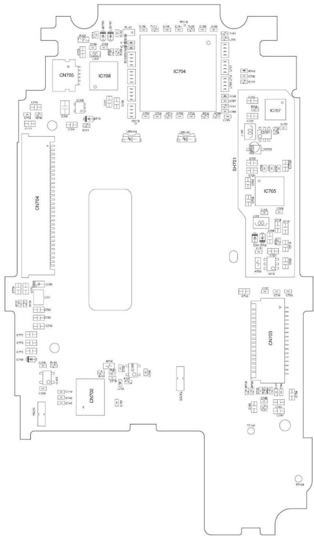
text_image
CN704 CN705 CN702 IC708 IC704 SH701 CN703 IC705 IC702 TCLV1 C718 C729 C730 C731 C732 C733 C734 C735 C736 C737 C738 C739 C740 C741 C742 C743 C744 C745 C746 C747 C748 C749 C750 C751 C752 C753 C754 L116 L117 L118 L119 L120 L121 L122 L123 L124 L125 L126 L127 L128 L129 L130 L131 L132 L133 L134 L135 L136 L137 L138 L139 L140 L141 L142 L143 L144 L145 L146 L147 L148 L149 L150 L151 L152 L153 L154 L155 L156 L157 L158 L159 L160 L161 L162 L163 L164 L165 L166 L167 L168 L169 L170 L171 L172 L173 L174 L175 L176 L177 L178 L179 L180 L181 L182 L183 L184 L185 L186 L187 L188 L189 L190 L191 L192 L193 L194 L195 L196 L197 L198 L199 L200TM200 CIRCUIT DIAGRAM AND PWB LAYOUT
■ LCD PWB_REAR

text_image
CN701 C720 C741 C743 L7X CT88 C765 TP701 TP702 TP703 TP704 TP705 TP706 TP707 TP708 TP709 TP710 TP711 TP712 TP713 TP714 TP715 TP716 TP717 TP718 TP719 TP720 TP721 TP722 TP723 TP724 TP725 TP726 TP727 TP728 TP729 TP730 TP731 TP732 TP733 TP734 TP735 TP736 TP737 TP738 TP739 TP740 TP741 TP742 TP743 TP744 TP745 TP746 TP747 TP748 TP749 TP750 TP751 TP752 TP753 TP754 TP755 TP756 TP757 TP758 TP759 TP760 TP761 TP762 TP763 TP764 TP765 TP766 TP767 TP768 TP769 TP770 TP771 TP772 TP773 TP774 TP775 TP776 TP777 TP778 TP779 TP780 TP781 TP782 TP783 TP784 TP785 TP786 TP787 TP788 TP789 TP790 TP791 TP792TM200 CIRCUIT DIAGRAM AND PWB LAYOUT
CONFIDENTIAL
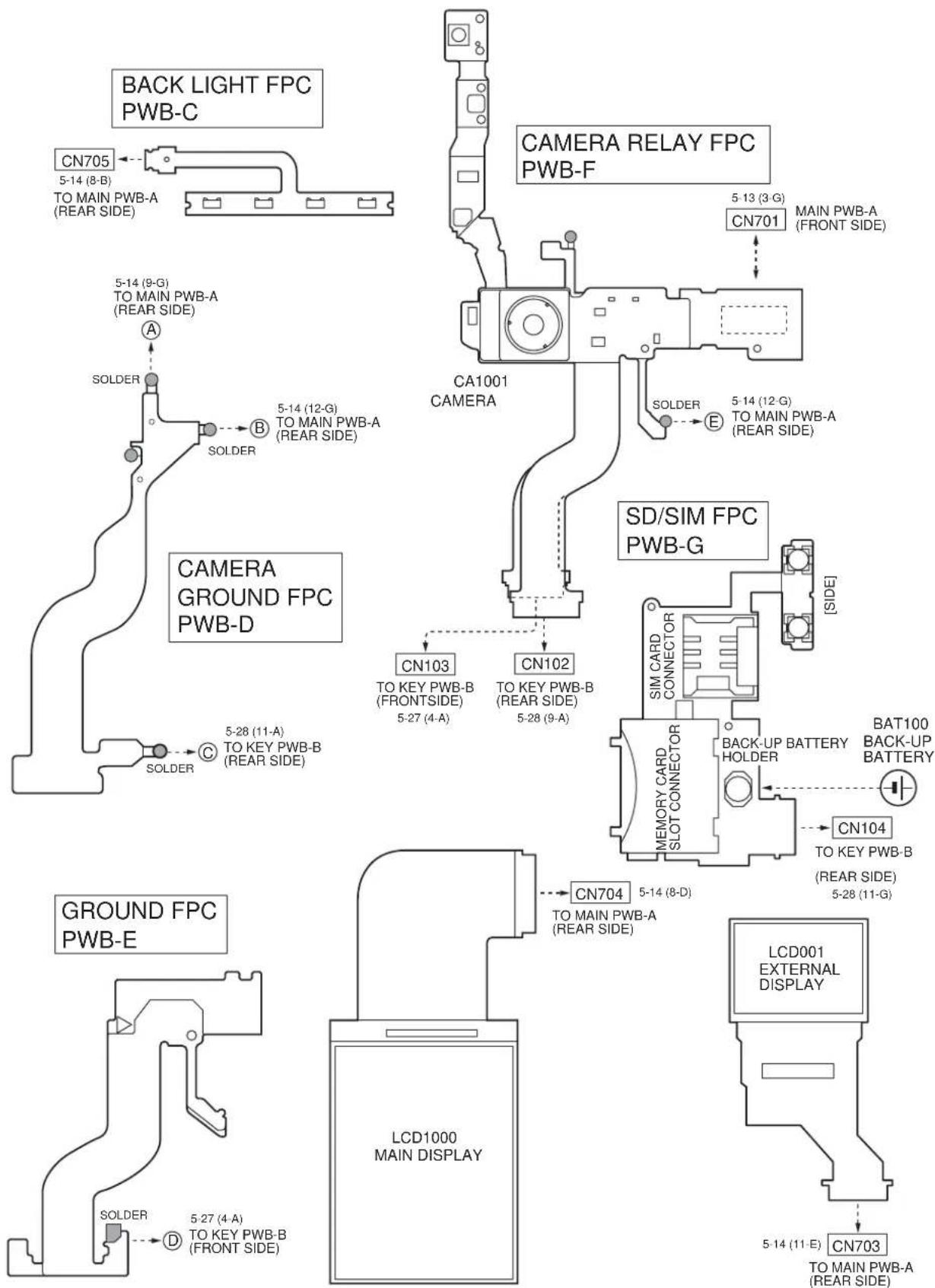
flowchart
graph TD
    A["BACK LIGHT FPC PWB-C"] --> B["CN705 5-14 (8-B) TO MAIN PWB-A (REAR SIDE)"]
    B --> C["SOLDER"]
    C --> D["5-14 (9-G) TO MAIN PWB-A (REAR SIDE)"]
    D --> E["SOLDER"]
    E --> F["5-14 (12-G) TO MAIN PWB-A (REAR SIDE)"]
    F --> G["SOLDER"]
    G --> H["5-28 (11-A) TO KEY PWB-B (REAR SIDE)"]
    H --> I["SOLDER"]
    I --> J["5-27 (4-A) TO KEY PWB-B (FRONT SIDE)"]

    K["CAMERA RELAY FPC PWB-F"] --> L["CA1001 CAMERA"]
    L --> M["SOLDER"]
    M --> N["5-13 (3-G) MAIN PWB-A (FRONT SIDE)"]
    N --> O["5-14 (12-G) TO MAIN PWB-A (REAR SIDE)"]
    O --> P["SOLDER"]
    P --> Q["5-14 (12-G) TO MAIN PWB-A (REAR SIDE)"]

    R["SD/SIM FPC PWB-G"] --> S["CN103 TO KEY PWB-B (FRONTSIDE) 5-27 (4-A)"]
    R --> T["CN102 TO KEY PWB-B (REAR SIDE) 5-28 (9-A)"]
    R --> U["SMICARD CONNECTOR"]
    U --> V["BACK-UP BATTERY HOLDER"]
    V --> W["BAT100 BACK-UP BATTERY"]
    W --> X["CN104 TO KEY PWB-B (REAR SIDE) 5-28 (11-G)"]

    Y["GROUND FPC PWB-E"] --> Z["SOLDER"]
    Z --> AA["5-27 (4-A) TO KEY PWB-B (FRONT SIDE)"]

    AB["LCD1000 MAIN DISPLAY"] --> AC["CN704 TO MAIN PWB-A (REAR SIDE)"]

    AD["LCD001 EXTERNAL DISPLAY"] --> AE["5-14 (11-E) CN703 TO MAIN PWB-A (REAR SIDE)"]
1 | 2 | 3 | 4 | 5 | 6
CONFIDENTIAL
Conditions: SIM card inserted, power on (battery=3.7V), in stand-by mode (opened)
Measuring instrument: Digital multimeter
——: Unmeasurable
| IC105 | |
| PIN NO. | VOLTAGE |
| 1 | 1.41V |
| 2 | 0V |
| 3 | 2.98V |
| 4 | 2.98V |
| 5 | — |
| 6 | 0V |
| 7 | 2.98V |
| 8 | 0V |
| 9 | 0V |
| 10 | 1.13V |
| 11 | 0.27V |
| 12 | — |
| 13 | 0V |
| 14 | 0V |
| 15 | 3.69V |
| 16 | 0V |
| 17 | 0V |
| 18 | 0V |
| 19 | 0V |
| 20 | 0.49V |
| 21 | 0.7V |
| 22 | 0.91V |
| 23 | 0.95V |
| 24 | 1.01V |
| 25 | 1.08V |
| 26 | 0.73V |
| 27 | 1.36V |
| 28 | 2.39V |
| 29 | 2.97V |
| 30 | 1.79V |
| 31 | 2.07V |
| 32 | 2.98V |
| IC111 | |
| PIN NO. | VOLTAGE |
| 1 | — |
| 2 | — |
| 3 | — |
| 4 | — |
| 5 | — |
| IC114 | |
| PIN NO. | VOLTAGE |
| 1 | — |
| 2 | — |
| 3 | — |
| 4 | — |
| 5 | — |
| IC115 | |
| PIN NO. | VOLTAGE |
| 1 | 0V |
| 2 | 0V |
| 3 | Not used |
| 4 | 0V |
- NOTES ON SCHEMATIC DIAGRAM can be found on page 5-1.
1 | 2 | 3 | 4 | 5 | 6
CONFIDENTIAL
CHAPTER 6. OTHERS
[1] FUNCTION TABLE OF IC
■ IC101 (LRS1B27): 5-LEVEL STACK MEMORY
| Pin No. | Terminal name | Input/Output | Description of terminal |
| 1 | NC | — | Not used |
| 2* | 20 Input Address input | (NOR Flash, Smartcombo RAM) | |
| 3 A | 11 Input Address input | (NOR Flash, Smartcombo RAM, SRAM) | |
| 4 A | 15 Input Address input | (NOR Flash, Smartcombo RAM, SRAM) | |
| 5 A | 14 Input Address input | (NOR Flash, Smartcombo RAM, SRAM) | |
| 6 A | 13 Input Address input | (NOR Flash, Smartcombo RAM, SRAM) | |
| 7 A | 12 Input Address input | (NOR Flash, Smartcombo RAM, SRAM) | |
| 8 | GND | — | Ground |
| 9 | NC | — | Not used (VCC IO/NC) |
| 10* | NC | — | Not used |
| 11* | NC | — | Not used |
| 12* | NC | — | Not used |
| 13* | SF-RY/BY Output Ready busy output(Smartcombo Flash) | ||
| 14 A | 16 Input Address input | (NOR Flash, Smartcombo RAM, SRAM) | |
| 15 A | 8 Input Address input | (NOR Flash, Smartcombo RAM, SRAM) | |
| 16 A | 10 Input Address input | (NOR Flash, Smartcombo RAM, SRAM) | |
| 17 A | 9 Input Address input | (NOR Flash, Smartcombo RAM, SRAM) | |
| 18 D | Q15 Input/Output Data input/output(NOR Flash, Smartcombo RAM, SRAM)Command, Address, and Datainput/output (Smartcombo Flash) | ||
| 19 | S/SC-/WE | Input | Write enable input(SRAM, Smartcombo RAM) |
| 20 | DQ14 Input/Output Data input/output(NOR Flash, Smartcombo RAM, SRAM)Command, Address, and Datainput/output (Smartcombo Flash) | ||
| 21 DQ7 | Input/Output Data input/output(NOR Flash, Smartcombo RAM, SRAM)Command, Address, and Datainput/output (Smartcombo Flash) | ||
| 22 NC | — | Not used | |
| 23* | NC | — | Not used |
| 24* | SF-/RE | Input Read | enable input(Smartcombo Flash) |
| 25 F | -/WE | Input Write | enable input (NOR Flash) |
| 26* | -RY/-BY | Output Ready busy output (NOR Flash)When deleting/writing: VOLWhen interrupting block delete/write: High-Z (High impedance) | |
| 27 A | 21 Input Address input | (NOR Flash, Smartcombo RAM 2) | |
| Pin No. | Terminal name | Input/Output | Description of terminal |
| 28 | SC2-CE2 | Input Sleep | state input(Smartcombo RAM 2) |
| 29 | DQ13 | Input/Output | Data input/output(NOR Flash, Smartcombo RAM, SRAM)Command, Address, and Data input/output (Smartcombo Flash) |
| 30 | DQ6 | Input/Output | Data input/output(NOR Flash, Smartcombo RAM, SRAM)Command, Address, and Data input/output (Smartcombo Flash) |
| 31 | DQ4 | Input/Output | Data input/output(NOR Flash, Smartcombo RAM, SRAM)Command, Address, and Data input/output (Smartcombo Flash) |
| 32 | DQ5 | Input/Output | Data input/output(NOR Flash, Smartcombo RAM, SRAM)Command, Address, and Data input/output (Smartcombo Flash) |
| 33 | NC | — | Not used |
| 34 | SF/F/SC-VCC | — | Power (NOR Flash ,Smartcombo Flash, Smartcombo RAM) |
| 35 | GND | — | Ground |
| 36 /RST | Input Reset | input (NOR Flash) (F-/RST)When deleting block/writing: VIHWhen reading : VIHReset : VIL | |
| 37 | A22 Input Address | input (NOR | Flash) |
| 38 | SC2-/CE1/NC(F2-/CE) | Input Chip | enable input(Smartcombo RAM 2) |
| 39 | DQ12 | Input/Output | Data input/output(NOR Flash, Smartcombo RAM, SRAM)Command, Address, and Data input/output (Smartcombo Flash) |
| 40 | S/SC1-CE2 | Input Chip | enable input (SRAM), sleep state input (Smartcombo RAM 1) |
| 41 | S-VCC | — | Power (SRAM) |
| 42 | SF/F/SC-VCC | — | Power (NOR Flash ,Smartcombo Flash, Smartcombo RAM) |
| 43 | NC | — | Not used |
| 44 | CLE | Input Command | latch enable input(Smartcombo Flash) |
| 45 | WP (F-/WP) | Input Write | protect input (NOR Flash) |
| 46 | VPP (F-VPP) | Input/- Power | voltage detect terminal(NOR Flash)When deleting/writing: VPP = VPPHWhen deleting/writing is prohibited: VPP < VPPLK |
| 47 | A19 Input Address | input | |
| 48 | DQ11 | Input/Output | Data input/output(NOR Flash, Smartcombo RAM, SRAM)Command, Address, and Data input/output (Smartcombo Flash) |
| 49 | SF/F/SC-VCC | — | Power (Flash, Smartcombo RAM) |
CONFIDENTIAL
| Pin No. | Terminal name | Input/Output | Description of terminal |
| 50 | DQ10 Input/Output | Data input/output | (NOR Flash, Smartcombo RAM, SRAM)Command, Address, and Data input/output (Smartcombo Flash) |
| 51 | DQ2 Input/Output | Data input/output | (NOR Flash, Smartcombo RAM, SRAM)Command, Address, and Data input/output (Smartcombo Flash) |
| 52 | DQ3 Input/Output | Data input/output | (NOR Flash, Smartcombo RAM, SRAM)Command, Address, and Data input/output (Smartcombo Flash) |
| 53*NC | — | Not used | |
| 54 | ALE Input Address | latch enable input(Smartcombo Flash) | |
| 55 | LB Input Byte enable input (DQ0-DQ7)(Smartcombo RAM, SRAM) | ||
| 56*UB Input Byte enable input (DQ8-DQ15)(Smartcombo RAM, SRAM) | |||
| 57 NC | — | Not used | |
| 58*NC | — | Not used | |
| 59 | DQ9 Input/Output | Data input/output | (NOR Flash, Smartcombo RAM, SRAM)Command, Address, and Data input/output (Smartcombo Flash) |
| 60 | DQ8 Input/Output | Data input/output | (NOR Flash, Smartcombo RAM, SRAM)Command, Address, and Data input/output (Smartcombo Flash) |
| 61 | DQ0 Input/Output | Data input/output | (NOR Flash, Smartcombo RAM, SRAM)Command, Address, and Data input/output (Smartcombo Flash) |
| 62 | DQ1 Input/Output | Data input/output | (NOR Flash, Smartcombo RAM, SRAM)Command, Address, and Data input/output (Smartcombo Flash) |
| 63*NC | — | Not used | |
| 64*NC | — | Not used | |
| 65 | SF-/WE Input Write enable input | (Smartcombo Flash) | |
| 66 | A18 Input Address input | (NOR Flash, Smartcombo RAM) | |
| 67 | A17 Input Address input | (NOR Flash, Smartcombo RAM, SRAM) | |
| 68 | A7 Input Address input | (NOR Flash, Smartcombo RAM, SRAM) | |
| 69 | A6 Input Address input | (NOR Flash, Smartcombo RAM, SRAM) | |
| 70 | A3 Input Address input | (NOR Flash, Smartcombo RAM, SRAM) | |
| 71 | A2 Input Address input | (NOR Flash, Smartcombo RAM, SRAM) | |
| 72 | A1 Input Address input | (NOR Flash, Smartcombo RAM, SRAM) | |
| 73 | SC1-/CE1 Input Chip enable input | (Smartcombo RAM 1) | |
| 74*NC | — | Not used | |
| 75*NC | — | Not used | |
| 76*NC | — | Not used | |
| Pin No. | Terminal name | Input/Output | Description of terminal |
| 77 | SF-/WP Input Write protect input | (Smartcombo Flash) | |
| 78 | SF-/CE | Input Chip enable input(Smartcombo Flash) | |
| 79 | A5 Input Address input | (NOR Flash, Smartcombo RAM, SRAM) | |
| 80 | A4 Input Address input | (NOR Flash, Smartcombo RAM, SRAM) | |
| 81 | A0 Input Address input | (NOR Flash, Smartcombo RAM, SRAM) | |
| 82 | F-/CE (F1-/CE) | Input Chip enable input (NOR Flash) | |
| 83 | GND | — | Ground |
| 84 | /OE | Input Output enable input(NOR Flash, Smartcombo RAM, SRAM) | |
| 85 | S-/CE1 | Input Chip enable input (SRAM) | |
| 86 | NC | — | Not used |
| 87 | NC | — | Not used |
In this unit, the terminal with asterisk mark (*) is (open) terminal which is not connected to the outside.
(TOPVIEW)
| 1 | 2 | 3 | 4 | 5 | 6 | 7 | 8 | 9 | 10 | 11 | 12 | |
| A | 1NC | 2A20 | 3A11 | 4A15 | 5A14 | 6A13 | 7A12 | 8GND | 9NC | 10NC | 11NC | |
| B | 12NC | 13BF-WB | 14A16 | 15A8 | 16A10 | 17A9 | 18DQ15 | 19SCW7 | 20DO14 | 21DO7 | 22NC | 23NC |
| C | 24SF-RE | 25F-WE | 26F-ZS | 27A21 | 28DQ1E | 29DQ13 | 30DO8 | 31DO4 | 32DO5 | 33NC | ||
| D | 34KXZT | 35GND | 36RST | 37A22 | 38CZENW | 39DQ12 | 40SJKZE | 41S-VCC | 42RCKW | 43NC | ||
| E | 44CLE | 45WP | 46VPP | 47A19 | 48DQ11 | 49PRXJ7 | 50DQ10 | 51DO2 | 53DO3 | 53NC | ||
| F | 54ALE | 55JLB | 56UJB | 57NC | 58NC | 59DQ9 | 60DO8 | 61DO5 | 62DO1 | 63NC | ||
| G | 64NC | 65SF-WE | 66A16 | 67A17 | 68A7 | 69A6 | 70A3 | 71A2 | 72A1 | 73(SI39) | 74NC | 75NC |
| H | 76NC | 77SF-WB | 78SF-CE | 79A6 | 80A4 | 81A0 | 82F-CE | 83GND | 84VOE | 85S-CE | 86NC | 87NC |
![SHARP TM200 - [1] FUNCTION TABLE OF IC - 1](/content/2026/06/1212016/images/bbe3edb7c3959440f3e50826da03748b4f75999b581bdae7cb38894eebdcc075.jpg)
flowchart
graph TD
    A["A22"] --> B["128M (x16) bit NOR Flash memory"]
    C["A21"] --> B
    D["A0~A17"] --> B
    E["A18~A20"] --> B
    F["F-/WE,/WP,/RST"] --> B
    G["/OE"] --> B
    H["F-/CE"] --> B
    I["SF-/WE,SF-/WP"] --> B
    J["ALE,CLE,SF-/RE"] --> B
    K["SF-/CE"] --> B
    L["S/SC-/WE/LB/UB"] --> M["SC1: 32M (x16) bit Smartcombo RAM"]
    N["SC1-/CE1"] --> M
    O["S/SC1-CE2"] --> M
    P["SC2-/CE1"] --> Q["SC2: 64M (x16) bit Smartcombo RAM"]
    R["SC2-CE2"] --> Q
    S["S-/CE1"] --> T["4M (x16) bit SRAM"]
    U["GND"] --> V["S-VCC"]
    W["VPP"] --> X["F-RY/-BY"]
    Y["SF/F/SC-VCC"] --> Z["SF-RY/BY"]
    AA["DQ0~DQ15"] --> AB["DQ0~DQ15"]
    AC["GND"] --> AD["S-VCC"]
CONFIDENTIAL
■ IC103 (AD6535): ANALOG BASEBAND
| Pin No. | Terminal name | Input/ Output | Description of terminal |
| 1 †DI Input Not used | |||
| 2 VCXOEN Input VCXO supply | |||
| 3 VBAT3 Input External interface regulator input | |||
| 4 VEXT Output Not used | |||
| 5 VCHG Input Charge supply | |||
| 6 GATEDRIVE Output Charge DAC (FET) output control | |||
| 7 ISENSE Input Charge current sense input | |||
| 8 TEMP2 Input Temp sensor input for battery | |||
| 9 AUXADC2 Input Not used | |||
| 10 REFBB Output Baseband transmit & receive voltage reference | |||
| 11 AGND2 | — | Analog baseband ground | |
| 12 IP Input/Output I-channel positive input/output | |||
| 13 IN Input/Output I-channel negative input/output | |||
| 14 QN Input/Output Q-channel positive input/output | |||
| 15 QP Input/Output Q-channel negative input/output | |||
| 16 RSVD_A16 | — | Not used | |
| 17 †MS | Input Not used | ||
| 18 †CK | Input Not used | ||
| 19 VBAT3 Input External interface regulator input | |||
| 20 VEXT Output Not used | |||
| 21 CHGOSC | Input Charge oscillator capacitor | ||
| 22 BATTYPE | Input Battery type identification input | ||
| 23 CHGDACREF | Output Charge DAC reference | ||
| 24 VBATSENSE | Input Battery voltage sense input | ||
| 25 TEMP1 | Inpsut Temp sensor input for camera | ||
| 26 AUXADC1 Input Auxiliary ADC input for temp. sensor adjustment | |||
| 27 REFOUT | Output Voltage reference output | ||
| 28 PA | Output Power amplifier control output | ||
| 29 AGND0 | — | Analog ground | |
| 30 AFCDAC | Output | Automatic frequency control DAC output | |
| 31 REF | Output Voltage reference | ||
| 32 AGND1 | — | Analog ground | |
| 33 †DO | Output Not used | ||
| 34 GPI | Input Not used | ||
| 35 VBAT1 Input Voltage controlled crystal oscillator regulator input | |||
| 36 RSVD_C16 | — | Not used | |
| 37 INT | Output Digital BB interrupt | ||
| 38 ASDO | Output Audio serial port data output | ||
| 39 REFCHG | Output Voltage reference output | ||
| 40 VVCXO | Output | Voltage controlled crystal oscillator supply 2.71 - 2.79 V (VT) | |
| 41 ASDI | Input Audio serial port data input | ||
| 42 BSDO | Output Baseband serial port data output | ||
| 43 VUSB | Output USB interface supply 3.0 - 3.6 V | ||
| 44 VAPPGATE | Output Application regulator pass device gate control | ||
| 45 BSIFS Input | Baseband serial port input framing signal | ||
| 46 ASFS Output Audio serial port framing signal | |||
| 47 VUSBIN Input USB interface regulator input | |||
| 48 VAPP | Output Application supply 2.75 - 3.3 V | ||
| 49 BSOFS | Output Baseband serial port output framing signal | ||
| Pin No. | Terminal name | Input/ Output | Description of terminal |
| 50 B | SDI | Input Baseband serial port data input | |
| 51 V | BAT2 Input Analog baseband | regulator input | |
| 52*NC_G16 | — | Not used | |
| 53 C | SDO | Output Control serial port data output | |
| 54 C | SDI | Input Control serial port data input | |
| 55 V | BAT2 Input Analog baseband | regulator input | |
| 56 V | ABB | Output Analog baseband supply | |
| 57 ASM | Input Advanced state machine | ||
| 58 M | CLKEN | Output Master clock enable | |
| 59 A | OUT1P | Output Receiver audio positive output | |
| 60 | AOUT3L | Output | Headset receiver audio L-channel output |
| 61 R | XON Input Baseband receive section control | ||
| 62 | TXON | Input | Baseband transmit section control |
| 63 | AOUT1N | Output | Receiver audio negative output |
| 64 | AOUT3R | Output | Headset receiver audio R-channel output |
| 65 M | CLK | Input Master clock | |
| 66 | CSFS | Input | Control serial port framing signal |
| 67 | AGND3 | — | Analog audio ground |
| 68 | LIGHT1 | Output | Charge LED control |
| 69 | ABBRESET | Input | Reset input |
| 70 | DGND | — | Digital ground |
| 71 | LIGHT2 | Output | USB charge enable |
| 72 L | LIGHT3 | Output Key-pad LED control | |
| 73 | VCORE | Output | Digital core supply 1.72 - 1.9 V |
| 74 | VCOREIN | Input | Digital core regulator input |
| 75 | LGND | — | Light driver ground |
| 76 | VMIC | Output | Microphone supply 2.4 - 2.6 V |
| 77 | VCORE | Output | Digital core supply 1.72 - 1.9 V |
| 78 | VMEMIN | Input | Memory interface regulator input |
| 79 | AIN2P | Input | Headset mic audio positive input |
| 80 | AIN1P | Input | Mic audio positive input |
| 81 | CRST | Output | Power-on reset capacitor |
| 82 | VMEMIN | Input | Memory interface regulator input |
| 83 | VMEMSEL | Input | Memory supply voltage selection |
| 84 | VBAT5 | Input | Back-up battery regulator input |
| 85 | VBAT4 | Input | SIM interface regulator input |
| 86 | VRTCIN | Input | Real-time clock regulator input |
| 87 | DBBON | Input | Digital BB supply regulator on signal |
| 88 S | GND | — | AOUT2P/N ground |
| 89* | AOUT2N | Output | Not used |
| 90*S | PWR Input Not used | ||
| 91* | AOUT2P | Output Not used | |
| 92* | NC_R12 | — | Not used |
| 93 | AIN3L | Input | Sound IC audio L-channel input |
| 94 | AIN3R | Input | Sound IC audio R-channel input |
| 95 | AIN2N | Input | Headset mic audio negative input |
| 96 | AIN1N | Input | Mic audio negative input |
| 97 | RESET Output | Reset output | |
| 98 V | MEM | Output | Memory interface supply 2.75 - 3.05 V |
| 99 V | MEM | Output | Memory interface supply 2.75 - 3.05 V |
| 100 | VBACK | Output | Backup battery supply 2.72 - 3.05 V |
| 101 | VBACKSEL | Input | Backup battery supply voltage selection |
CONFIDENTIAL
| Pin No. | Terminal name | Input/ Output | Description of terminal |
| 102 VSIM Output SIM interface supply 2.75 - 2.95 V | |||
| 103 VRTC Output Real-time clock supply 1.6 - 2.0 V | |||
| 104 SGND | — | AOUT2P/N ground | |
| 105* AOUT2N Output Not used | |||
| 106* SPWR Input Not used | |||
| 107* AOUT2P Output Not used | |||
| 108 LDOEN Output Regulator enable output | |||
| 109 KEYOUT Output Power-on key output | |||
| 110 KEYON Input Power-on key input | |||
| 111 IBIAS Output Regulator bias current reference | |||
| 112 AGND4 | — | Power management analog ground | |
| 113 AGND0 | — | Thermal ground for power supply | |
| 114 AGND0 | — | Thermal ground for power supply | |
| 115 AGND0 | — | Thermal ground for power supply | |
| 116 AGND0 | — | Thermal ground for power supply | |
| 117 AGND0 | — | Thermal ground for power supply | |
| 118 AGND0 | — | Thermal ground for power supply | |
| 119 AGND0 | — | Thermal ground for power supply | |
| 120 AGND0 | — | Thermal ground for power supply | |
| 121 AGND0 | — | Thermal ground for power supply | |
| 122 AGND0 | — | Thermal ground for power supply | |
| 123 AGND0 | — | Thermal ground for power supply | |
| 124 AGND0 | — | Thermal ground for power supply | |
| 125 AGND0 | — | Thermal ground for power supply | |
| 126 AGND0 | — | Thermal ground for power supply | |
| 127 AGND0 | — | Thermal ground for power supply | |
| 128 AGND0 | — | Thermal ground for power supply | |
| 129 AGND0 | — | Thermal ground for power supply | |
| 130 AGND0 | — | Thermal ground for power supply | |
| 131 AGND0 | — | Thermal ground for power supply | |
| 132 AGND0 | — | Thermal ground for power supply | |
| 133 AGND0 | — | Thermal ground for power supply | |
| 134 AGND0 | — | Thermal ground for power supply | |
| 135 AGND0 | — | Thermal ground for power supply | |
| 136 AGND0 | — | Thermal ground for power supply | |
| 137 AGND0 | — | Thermal ground for power supply | |
| 138 AGND0 | — | Thermal ground for power supply | |
| 139 AGND0 | — | Thermal ground for power supply | |
| 140 AGND0 | — | Thermal ground for power supply | |
| 141 AGND0 | — | Thermal ground for power supply | |
| 142 AGND0 | — | Thermal ground for power supply | |
| 143 AGND0 | — | Thermal ground for power supply | |
| 144 AGND0 | — | Thermal ground for power supply | |
| 145 AGND0 | — | Thermal ground for power supply | |
| 146 AGND0 | — | Thermal ground for power supply | |
| 147 AGND0 | — | Thermal ground for power supply | |
| 148 AGND0 | — | Thermal ground for power supply | |
In this unit, the terminal with asterisk mark (*) is (open) terminal which is not connected to the outside.
■ IC105 VHIYMU762C+-1L (YMU762C): SOUND
| Pin No. | Terminal name | Input/Output | Description of terminal |
| 1 | CLKI | Input | Clock input terminal |
| 2 | LED | Output | External LED control terminal |
| 3 | /IRQ | Output | Interrupt output terminal |
| 4 | /RST | Input | Hardware reset input terminal |
| 5* | NC | — | Not used |
| 6 | PLLC | — | Built-in PLL capacitor terminal |
| 7 | VDD | — | Power supply (Typ + 3.0 V) |
| 8 | VSS | — | Ground |
| 9 | VREF | — | Analog reference voltage terminal |
| 10 | HPOUT-L/MONO | Output | Headphone output L-ch |
| 11 | HPOUT-R Output | Headphone output R-ch | |
| 12 | EQ1 | — | Equalizer terminal 1 |
| 13 | EQ2 | — | Equalizer terminal 2 |
| 14 | EQ3 | — | Equalizer terminal 3 |
| 15 | SPVDD | — | Analog power supply for speaker amplifier (Typ + 3.6 V) |
| 16 | SPVSS | — | Analog ground for speaker amplifier |
| 17 | SPOUT1 | Output | Speaker terminal 1 |
| 18 | SPOUT2 | Output | Speaker terminal 2 |
| 19 | MTR | Output | External motor control terminal |
| 20 | D7 | Input/Output | CPU I/F data bus 7 |
| 21 | D6 | Input/Output | CPU I/F data bus 6 |
| 22 | D5 | Input/Output | CPU I/F data bus 5 |
| 23 | D4 | Input/Output | CPU I/F data bus 4 |
| 24 | D3 | Input/Output | CPU I/F data bus 3 |
| 25 | D2 | Input/Output | CPU I/F data bus 2 |
| 26 | D1 | Input/Output | CPU I/F data bus 1 |
| 27 | D0 | Input/Output | CPU I/F data bus 0 |
| 28 | /WR | Input | CPU I/F write enable |
| 29 | /CS | Input | CPU I/F chip select input |
| 30 | A0 | Input | CPU I/F address signal |
| 31 | /RD | Input | CPU I/F read enable |
| 32 | IOVDD | — | Power supply for terminal |
In this unit, the terminal withasterisk mark (*) is (open) terminal which is not connected to the outside.
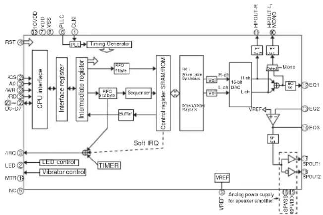
flowchart
graph TD
    A["CPU Interface"] --> B["Interface register"]
    B --> C["Intermediate register"]
    C --> D["RFO 1/2 Data"]
    D --> E["Sequence"]
    E --> F["Control register SHAM/HOM"]
    F --> G["PWM/ROM Request"]
    G --> H["16-bit DAC L-ch"]
    H --> I["VREF"]
    I --> J["Analog power supply for speaker amplifier"]
    J --> K["SPVSS SPVD"]
    K --> L["SPOUT1"]
    K --> M["SPOUT2"]
    N["ACS ②"] --> O["CPU interface"]
    P["AD ③"] --> O
    Q["NR ④"] --> O
    R["WD ⑤"] --> S["LLED control"]
    T["MTR ⑥"] --> U["Vibrator control"]
    V["RF0 ⑦"] --> W["Suffar"]
    X["Soft IRQ"] -.-> Y["TIMER"]
    Z["HPOUT-R"] --> AA["Power Supply"]
    AB["HPOUT-L"] --> AC["Power Supply"]
    AD["HDWR"] --> AE["Power Supply"]
    AF["ADC"] --> AG["Power Supply"]
    AH["ADC"] --> AI["Power Supply"]
    AJ["ADC"] --> AK["Power Supply"]
    AL["ADC"] --> AM["Power Supply"]
    AN["ADC"] --> AO["Power Supply"]
    AP["ADC"] --> AQ["Power Supply"]
    AR["ADC"] --> AS["Power Supply"]
    AT["ADC"] --> AU["Power Supply"]
    AV["ADC"] --> AW["Power Supply"]
    AX["ADC"] --> AY["Power Supply"]
    AZ["ADC"] --> BA["Power Supply"]
    BB["ADC"] --> BC["Power Supply"]
    BD["ADC"] --> BE["Power Supply"]
    BF["ADC"] --> BG["Power Supply"]
    BH["ADC"] --> BI["Power Supply"]
    BJ["ADC"] --> BK["Power Supply"]
    BL["ADC"] --> BM["Power Supply"]
    BN["ADC"] --> BO["Power Supply"]
    BP["ADC"] --> BQ["Power Supply"]
    BR["ADC"] --> BS["Power Supply"]
    BT["ADC"] --> BU["Power Supply"]
    BV["ADC"] --> BW["Power Supply"]
    BX["ADC"] --> BY["Power Supply"]
    BZ["ADC"] --> BQ
    CA["ADC"] --> BQ
    CB["ADC"] --> BQ
    CC["ADC"] --> BQ
    CD["ADC"] --> BQ
    CE["ADC"] --> BQ
    CF["ADC"] --> BQ
    CG["ADC"] --> BQ
    CH["ADC"] --> BQ
    CI["ADC"] --> BQ
    CJ["ADC"] --> BQ
    CK["ADC"] --> BQ
CONFIDENTIAL
■ IC106 (AD6529B): DIGITAL BASEBAND
| Pin No. | Terminal name | Input/ Output | Description of terminal |
| 1 | ASDO Output Audio | serial port | data output to analog BB |
| 2 | BSDI Input | Baseband serial port data input from analog BB | |
| 3 | BSOFS Output Base | band serial | port output framing signal output to analog BB |
| 4 | GPIO_48 Input Hook | switch of h | hands free kit (earphone) detection |
| 5 | VNT Input Analog BB | interface | power supply 1.7 - 3.3 V (VCORE) |
| 6 | GPO_29 Output | Analog BB reset output (ABBRESET) | |
| 7 | GPO_5 Output | Advanced state machine of analog BB | |
| 8 | VDDRTC Input RTC | power supply | 1.0 - 1.9 V (VRTC) |
| 9 | VSSRTC | — | RTC ground |
| 10 | MC_DAT[0] | Input/ Output | SD interface data bus 0 |
| 11 | GPIO_22 Output RSP for main | LCD controller | |
| 12 | GPIO_56 Input Boot control 2 | (Hardware version select) | |
| 13 | KEYPADCOL[4] Output KEYIN | signal output 4 | |
| 14 | KEYPADCOL[1] Output KEYIN | signal output 1 | |
| 15 | KEYPADROW[4] | Input KE | YIN signal input 4 |
| 16 | KEYPADROW[2] | Input KE | YIN signal input 2 |
| 17 | GPIO_38 Input Interrupt input from sound generator IC | ||
| 18 | GPIO_36 Output Mode select 2 | for interface IC/ AOUT3 bias control | |
| 19 | ASDI Input Audio serial port data | input from analog BB | |
| 20 | GPIO_35 Input SD card interface write protect | ||
| 21 | ADD[0] Output Write protect control for flash memory 2 | ||
| 22 | ASFS | Input | Audio serial port framing signal input from analog BB |
| 23 | BSIFS | Input | Baseband serial port input framing signal input from analog BB |
| 24 | BSDO | Output | Baseband serial port data output to analog BB |
| 25 | CSDI | Input | Control serial port data input from analog BB |
| 26 | GPO_6 Output Not used | ||
| 27 | GPO_0 | Output | Analog baseband receive section control (RXON) |
| 28 | OSCOUT Output 32.768 kHz crystal oscillator output | ||
| 29 | MC_DAT[2] | Input/ Output | SD interface data bus 2 |
| 30 | VMC | Input | SD card interface power supply 1.7 - 3.3 V (VAPP) |
| 31 | VCC | Input | Core power supply 1.7 - 1.9 V (VCORE) |
| 32 | KEYPADCOL[3] Output KEYIN | signal output 3 | |
| 33 | KEYPADCOL[2] Output KEYIN | signal output 2 | |
| 34 | GPIO_39 Output USB PU control for interface IC | ||
| 35 | GPIO_37 Input Interrupt input from analog BB | ||
| Pin No. | Terminal name | Input/ Output | Description of terminal |
| 36 | GPIO_34 Output UART_TXD for Bluetooth module | ||
| 37 | ADD[4] Output Processor address bus 4 | ||
| 38 | ADD[2] Output Processor address bus 2 | ||
| 39 | GND | — | Ground |
| 40 | KEYPADROW[0] | Input | KEYIN signal input 0 |
| 41 | VEXT | Input | System interface power supply 2.4 - 3.3 V (VINT) |
| 42 | GPO_23 Output SLEEP control for SRAM 2 | ||
| 43 | ADD[7] Output Processor address bus 7 | ||
| 44 | VMEM | Input | Memory power supply 2.7 - 3.3 V (VMEM) |
| 45 | ADD[1] Output Processor address bus 1 | ||
| 46 | CSDO | Output | Control serial port data output to analog BB |
| 47 | CLKOUT_GATE | Input | Master clock enable from analog BB (MCLKEN) |
| 48 | GPO_1 | Output | Analog baseband transmit section control (TXON) |
| 49 | OSCIN Input 32.768 kHz crystal oscillator input | ||
| 50 | MC_CMD Input/ | Output | SD interface CMD (SD_CMD) |
| 51 | GPIO_55 | Input | Boot control 1 (Hardware version select) |
| 52 | GND | — | Ground |
| 53 | KEYPADROW[3] | Input KEYIN signal input 3 | |
| 54 | KEYPADROW[1] | Input KEYIN signal input 1 | |
| 55 | GPIO_33 Input UART_RXD for Bluetooth module | ||
| 56 | GPIO_17 | Output | PCM data output for Bluetooth module |
| 57 | ADD[11] Output Processor address bus 11 | ||
| 58 | ADD[9] Output Processor address bus 9 | ||
| 59 | ADD[5] Output Processor address bus 5 | ||
| 60 | ADD[3] Output Processor address bus 3 | ||
| 61 | GND | — | Ground |
| 62 | VCC | Input | Core power supply 1.7 - 1.9 V (VCORE) |
| 63 | PWRON | Output | System power control for analog BB |
| 64 | MC_DAT[1] | Input/ Output | SD interface data bus 1 |
| 65 | GND | — | Ground |
| 66 | VEXT | Input | SIM power supply 2.4 - 3.3 V (VINT) |
| 67 | KEYPADCOL[0] | Output | KEYIN signal output 0 |
| 68 | VEXT | Input | SIM power supply 2.4 - 3.3 V (VINT) |
| 69 | GPIO_15 | Input | PCM data input for Bluetooth module |
| 70 | GPIO_16 | Output | PCM SYNC output for Bluetooth module |
| 71 | ADD[13] Output Processor address bus 13 | ||
| 72 | ADD[12] Output Processor address bus 12 | ||
| 73 | ADD[8] Output Processor address bus 8 | ||
| 74 | ADD[6] Output Processor address bus 6 | ||
CONFIDENTIAL
| Pin No. | Terminal name | Input/ Output | Description of terminal |
| 75 | GPO_22 Output VPP control for flash memory 1 | ||
| 76 | GPIO_14 | Output | PCM clock output for Bluetooth module |
| 77 | GPIO_10 Input USB detection | ||
| 78 | GPIO_12 | Output | Reset output for main LCD controller/Sub LCD driver/Power management IC |
| 79 | VMEM | Input | Memory power supply 2.7 - 3.3 V (VMEM) |
| 80 | ADD[14] Output Processor address bus 14 | ||
| 81 | GND | — | Ground |
| 82 | VCC | Input | Core power supply 1.7 - 1.9 V (VCORE) |
| 83 | ADD[10] Output Processor address bus 10 | ||
| 84 | CLKOUT | Output | 13 MHz clock output for analog BB (CLKOUT) |
| 85 | MC_DAT[3] Input/ | Output | SD interface data bus 3 |
| 86 | GND | — | Ground |
| 87 | GND | — | Ground |
| 88 | GPIO_13 Input Interrupt input from camera module | ||
| 89 | GPIO_7 Input Hands free kit (earphone) detection | ||
| 90 | GPIO_9 | Input | Manufacturer specific input from I/O connector |
| 91 | ADD[19] Output Processor address bus 19 | ||
| 92 | ADD[17] Output Processor address bus 17 | ||
| 93 | ADD[18] Output Processor address bus 18 | ||
| 94 | ADD[15] Output Processor address bus 15 | ||
| 95 | ADD[16] Output Processor address bus 16 | ||
| 96 | GSFS | Output | Control serial port framing signal output to analog BB |
| 97 | MC_CLK Input SD interface clock (SD_CLK) | ||
| 98 | VCC | Input | Core power supply 1.7 - 1.9 V (VCORE) |
| 99 | GPIO_11 Input Flip switch detection | ||
| 100 | GPIO_8 | Input | Stereo/monaural detection for hands free kit (earphone) |
| 101 | GPIO_5 Input SD card detection | ||
| 102 | GPIO_6 | Input | Interrupt input from main LCD controller |
| 103 | ADD[22] Output Processor address bus 22 | ||
| 104 | ADD[21] Output Processor address bus 21 | ||
| 105 | GPIO_40 | Output | 13 MHz clock output for main LCD controller & Sound generator IC |
| 106 | ADD[20] Output Processor address bus 20 | ||
| 107 | GND | — | Ground |
| 108 | ADD[23] Output Processor address bus 23 | ||
| 109 | GND | — | Ground |
| 110 | VEXT | Input | SIM power supply 2.4 - 3.3 V (VINT) |
| 111 | GND | — | Ground |
| 112 | GPIO_4 Output UART_CTS for Bluetooth module | ||
| 113 | GPIO_2 Output USB charge current control | ||
| 114 | GPIO_3 Input UART_RTS for Bluetooth module | ||
| Pin No. | Terminal name | Input/ Output | Description of terminal |
| 115 | DATA[2] Input/ | Output | Processor data bus 2 |
| 116 | DATA[0] Input/ | Output | Processor data bus 0 |
| 117 | DATA[5] Input/ | Output | Processor data bus 5 |
| 118 | DATA[1] Input/ | Output | Processor data bus 1 |
| 119 | DATA[3] Input/ | Output | Processor data bus 3 |
| 120 | VCC | Input | Core power supply 1.7 - 1.9 V (VCORE) |
| 121 | DMINUS Input USB D- | ||
| 122 | GPIO_18 Output JTAG TCK | ||
| 123 | GND | — | Ground |
| 124 | GPIO_1 Input IrDA receive data | ||
| 125 | USC[5] | Input USC pin (CTS/Ginie_TX) | |
| 126 | GPIO_0 Output IrDA transmit data | ||
| 127 | DATA[4] Input/ | Output | Processor data bus 4 |
| 128 | VMEM | Input | SIM power supply 2.7 - 3.3 V (VMEM) |
| 129 | GND | — | Ground |
| 130 | VCC | Input | Core power supply 1.7 - 1.9 V (VCORE) |
| 131 | USC[6] | Input USC pin (GPIO_31/Ginie_RX) | |
| 132 | VCC | Input | Core power supply 1.7 - 1.9 V (VCORE) |
| 133 | USC[2] | Input USC pin (TXD) | |
| 134 | USC[4] | Input USC pin (RTS/Ginie_RX) | |
| 135 | DATA[7] Input/ | Output | Processor data bus 7 |
| 136 | DATA[6] Input/ | Output | Processor data bus 6 |
| 137 | GND | — | Ground |
| 138 | DATA[9] Input/ | Output | Processor data bus 9 |
| 139 | DATA[13] | Input/ Output | Processor data bus 13 |
| 140 | NROMCS1 | Output Chip select for flash memory 1 | |
| 141 | GPIO_42 Output Chip select for main LCD controller | ||
| 142 | CLKIN | Input 13 MHz clock input | |
| 143 | VSIM | Input | SIM power supply 1.7 - 3.3 V (VSIM) |
| 144 | GND | — | Ground |
| 145 | USC[3] | Input Pull up to VINT | |
| 146 | USC[1] | Input USC pin (RXD) | |
| 147 | GND | — | Ground |
| 148 | USC[0] | Input USC pin (Ginie_TX) | |
| 149 | DATA[10] | Input/ Output | Processor data bus 10 |
| 150 | DATA[8] Input/ | Output | Processor data bus 8 |
| 151 | NRD | Output Processor read strobe | |
| 152 | DATA[14] | Input/ Output | Processor data bus 14 |
CONFIDENTIAL
| Pin No. | Terminal name | Input/ Output | Description of terminal |
| 153 | GND | — | Ground |
| 154 | NRAMCS2 Output | Chip select | for SRAM 2 |
| 155 | GPIO_44 Input Wakeup mode | select | |
| 156 | VSSUSB | — | USB ground |
| 157 | GPIO_47 Output Camera module reset | ||
| 158 | GPIO_20 Output JTAG TDI | ||
| 159 | CLKON | Output | 13 MHz oscillator power control signal (VCXOEN) |
| 160 | VCC | Input | Core power supply 1.7-1.9V (VCORE) |
| 161 | GPO_18 Output SYNTH enable for RF (SYNTHEN) | ||
| 162 | GPO_21 | Output | SYNTH clock output for RF (SYNTHCLK) |
| 163 | DATA[12] Input/ | Output | Processor data bus 12 |
| 164 | DATA[11] Input/ | Output | Processor data bus 11 |
| 165 | NWE Output Processor write strobe | ||
| 166 | VEXT | Input | SIM power supply 2.4 - 3.3 V (VINT) |
| 167 | GPO_11 Output Band select 4 for RF (BS4) | ||
| 168 | GPO_20 | Output | SYNTH data output for RF (SYNTHDATA) |
| 169 | DATA[15] Input/ | Output | Processor data bus 15 |
| 170 | VMEM | Input | Memory power supply 2.7 - 3.3 V (VMEM) |
| 171 | NADV | Output | Address latch enable for flash memory 2 |
| 172 | NGPCS1 Output Chip select for flash memory 2 | ||
| 173 | VMEM | Input | Memory power supply 2.7 - 3.3 V (VMEM) |
| 174 | GPIO_45 Output Chip select for 4M SRAM | ||
| 175 | GPIO_46 Output Chip select for sound generator IC | ||
| 176 | DPLUS Input USB D+ | ||
| 177 | SIMCLK Output System interface clock output | ||
| 178 | JTAGEN Input JTAG enable | ||
| 179 | VEXT | Input | SIM power supply 2.4 - 3.3 V (VINT) |
| 180 | GPO_3 Output Incoming LED OFF control | ||
| 181 | GPO_4 Output Mode select 1 for interface IC | ||
| 182 | GPO_7 Output | Bluetooth module power ON/OFF control | |
| 183 | GPO_16 Output Band select 1 for RF (BS1) | ||
| 184 | GPO_17 Output Band select 2 for RF (BS2) | ||
| 185 | NHWR/NUSB | Output Processor high write strobe | |
| 186 | GPO_19 Output Mode select 3 for interface IC | ||
| 187 | NLWR/NLSB | Output Processor low write strobe | |
| 188 | NWAIT | Input Processor wait input | |
| 189 | NRESET | Input System reset input | |
| 190* | BURSTCLK | Output Not used | |
| 191 | NRAMCS1 Output Chip select for SRAM 1 | ||
| 192 | NAUXCS1 | Output | Command latch enable for flash memory 2 |
| 193 | GPIO_43 Output Chip select for Camera module | ||
| Pin No. | Terminal name | Input/ Output | Description of terminal |
| 194 | VDDUSB Input | USB power supply 2.8 - 3.3 V (VUSB) | |
| 195 | GPIO_23 Output SIM interface reset | ||
| 196 | SIMDATAIO | Input/ Output | SIM interface data input/output |
| 197 | GPIO_24 Output Sound generator IC reset | ||
| 198 | GPIO_19 Output JTAG TMS | ||
| 199 | GPIO_21 Output JTAG TDO | ||
| 200 | GPO_2 Output | Write protect control for flash memory 1 | |
| 201 | GND | — | Ground |
| 202 | GPO_8 Output IrDA power ON/OFF control | ||
| 203 | GPO_9 Output Band select 3 for RF (BS3) | ||
| 204 | GPO_10 Output BUF OFF for main LCD controller | ||
In this unit, the terminal with asterisk mark (*) is (open) terminal which is not connected to the outside.
■ IC107 VHIEW6671++-1R (EW6671): HALL
| Pin No. | Terminal name | Input/Output | Description of terminal |
| 1 | VDD | Input | Input |
| 2 | GND | — | Ground |
| 3 | OUT | Output | Output |
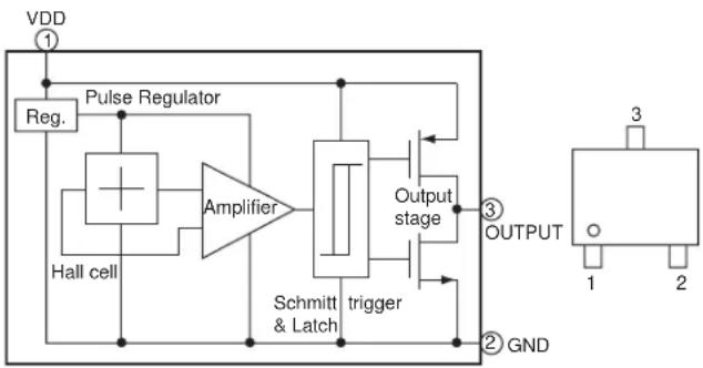
flowchart
graph TD
    A["VDD"] --> B["Reg."]
    B --> C["Pulse Regulator"]
    C --> D["Amplifier"]
    D --> E["Output stage"]
    E --> F["Schmitt & Latch trigger"]
    F --> G["GND"]
    H["Hall cell"] --> D
    I["3 OUTPUT"] --> J["1"]
    I --> K["2"]
■ IC108 VHIR3112Q26-1L (R3112Q261A): VOLTAGE DETECTOR
| Pin No. | Terminal name | Input/ Output | Description of terminal |
| 1 | VDD | — | Power supply |
| 2 | GND | — | Ground |
| 3 | CD | Input | External condenser connection terminal for delay |
| 4 | OUT | Output | Output terminal (L: when output is detected, H: when output is canceled) |

text_image
VDD① RD VREF + - CD ② GND ③ ④ OUTCONFIDENTIAL
■ IC109 VHINJ287130-1L (NJM2871F03): 3.0 V REGULATOR
| Pin No. | Terminal name | Input/ Output | Description of terminal |
| 1 | ONT Input Control | ||
| 2 | GND | — | Ground |
| 3 | NB | — | Noise bypass |
| 4 | OUT Output Output | ||
| 5 | IN Input Input | ||
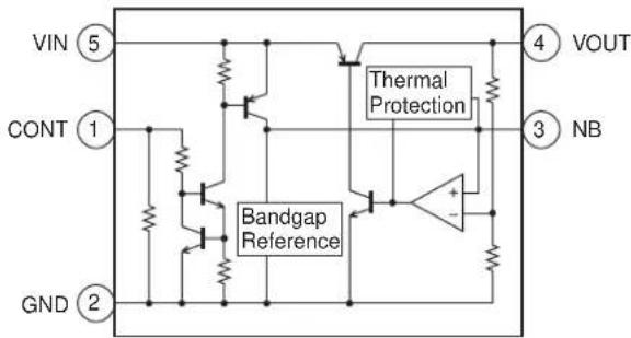
text_image
VIN ⑤ CONT ① GND ② Thermal Protection Bandgap Reference VOUT ④ 3 NB■ IC111 VHIR116030B-1L (R1160N301B): REGULATOR
■ IC703 VHIR116018B-1L (R116018B): 1.8 V REGULATOR
| Pin No. | Terminal name | Input/ Output | Description of terminal |
| 1 VDD Input Input | |||
| 2 | GND | — | Ground |
| 3 CE Input Chip enable | |||
| 4 ECO Input | High speed/low consumption selector switch | ||
| 5 VOUT Output Output | |||

text_image
VDD ① CE ③ VREF CURRENT LIMIT ECO ④ ⑤ VOUT ② GND■ IC113, 706 VHITC7SZ08A-1L (TC7SZ08A): AND GATE/LOGIC
| Pin No. | Terminal name | Input/ Output | Description of terminal |
| 1 A | Input Signal input | ||
| 2 B | Input Signal input | ||
| 3 | GND | — | Ground |
| 4 Y | Output Logic value output | ||
| 5 V | CC | Input Power supply | |
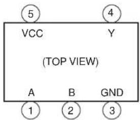
text_image
⑤ VCC Y (TOP VIEW) A B GND ① ② ③■ IC114 RH-IXA007AFZZL (HA1631S03CME): COMPARATOR
| Pin No. | Terminal name | Input/ Output | Description of terminal |
| 1 IN+ | Input Input | ||
| 2 | V SS | — | Ground |
| 3 IN- | Input Input | ||
| 4 VOUT | Output Output | ||
| 5 | VD D | — | Power supply |
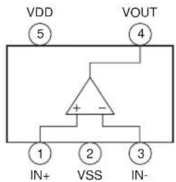
text_image
VDD 5 VOUT 4 + - 1 IN+ 2 VSS 3 IN-■ IC115 VHIXC61CN27-1L (XC61CN27): REGULATOR
| Pin No. | Terminal name | Input/ Output | Description of terminal |
| 1 VOUT | Output Output | ||
| 2 VIN | Input Supply voltage input | ||
| 3* | NC | — | Not used |
| 4 | GN D | — | Ground |
In this unit, the terminal withasterisk mark (*) is (open) terminal which is not connected to the outside.

text_image
VIN② + - VREF NC③ ① VOUT ④ VSS■ IC116 VHIRQ5RW45B-1L (RQ5RW45B): 4.5 V REGULATOR
| Pin No. | Terminal name | Input/ Output | Description of terminal |
| 1 | GND | — | Ground |
| 2 | VDD | — | Power supply |
| 3 VOUT Output Output | |||
| 4 CE Input Chip enable | |||

text_image
VDD② CE④ VREF CURRENT LIMIT ① GND ③ VOUTCONFIDENTIAL
■ IC502 VHIBU7870KN-1L (BU7870KN): USB CONTROLLER
| Pin No. | Terminal name | Input/ Output | Description of terminal |
| 1 MODESEL1 Input | Operation mode switching 1 | ||
| 2 MODESEL2 Input | Operation mode switching 2 | ||
| 3 UART_RXD Output | UART_RXD output | ||
| 4 UART_TXD Input | UART_TXD input | ||
| 5 C P U | V —D | Digital power supply | |
| 6 UART_RTS Input | UART_RTS input | ||
| 7 BSYNC Input BSYNC input | |||
| 8 UART_CTS Output | UART_CTS output | ||
| 9 BDATA Input BDATA input | |||
| 10 BCNT Input BDATA input control | |||
| 11 MODESEL3 Input | Operation mode switching 3 | ||
| 12 TXANOUT Output Hands | free sending external output | ||
| 13 RXANAIN | Input Hands free receiving external input | ||
| 14 GND1 | — | Ground | |
| 15 RXANOUT Output Hands | free receiving output | ||
| 16 TXANAIN | Input Hands free sending input | ||
| 17 NC | — | Not used | |
| 18 | BDATA/CTS | Input/ Output | BDATA/CTS switching external input/output |
| 19 | BSYNC/RTS | Output BSYNC/RTS switching external output | |
| 20 USBD-/TXD | Input/ Output | USBD-/TXD switching external input/output | |
| 21 GND2 | — | Ground | |
| 22 | USBD+/RXD | Input/ Output | USBD+/RXD switching external input/output |
| 23 | CPU_USB_D+ | Input/ Output | CPU_USB_D+ input/output |
| 24 | CPU_USB_D- | Input/ Output | CPU_USB_D- input/output |
| 25 REG33 | — | Power supply voltage for USB | |
| 26 PU15 Output PMOS open drain output | |||
| 27 PUEA Input PU15 control input | |||
| 28 GND3 | — | Ground | |
In this unit, the terminal withasterisk mark ( * ) is (open) terminal which is not connected to the outside.

flowchart
graph TD
    A["MODESEL1"] --> B["1"]
    C["MODESEL2"] --> D["2"]
    E["UART_RXD"] --> F["3"]
    G["UART_TXD"] --> H["4"]
    I["CPU USB D-23"] --> J["5"]
    K["CPU USB D-24"] --> L["6"]
    M["PU16 26"] --> N["7"]
    O["PUEA 27"] --> P["8"]
    Q["GND3 28"] --> R["9"]
    S["GND2"] --> T["10"]
    U["USB0-TXD"] --> V["11"]
    W["BSYNCIRTS"] --> X["12"]
    Y["DATACTS"] --> Z["13"]
    AA["NC"] --> AB["14"]
    AC["TXANAIN"] --> AD["15"]
    AE["RXANAOUT"] --> AF["16"]
    AG["GND1"] --> AH["17"]
    AI["GND2"] --> AJ["18"]
    AK["MODE 0.1.2 OFF MODE 1.5 ON"] --> AL["22"]
    AM["MODE 0.1.2 OFF MODE 2.0 OFF"] --> AN["23"]
    AO["MODE 0.1.2 OFF MODE 3.0 ON"] --> AP["24"]
    AQ["MODE 0.1.2 OFF MODE 4.0 OFF"] --> AR["25"]
    AS["MODE 0.1.2 OFF MODE 5.0 OFF"] --> AT["26"]
    AU["MODE 0.1.2 OFF MODE 6.0 OFF"] --> AV["27"]
    AW["MODE 0.1.2 OFF MODE 7.0 OFF"] --> AX["28"]
    AY["MODE SEL1"] --> AZ["3"]
    BA["MODE SEL2"] --> BB["4"]
    BC["MOSCELLS"] --> BD["MOSCELLS"]
    BE["BNT"] --> BF["MOSCELLS"]
    BG["BDATA"] --> BH["MOSCELLS"]
    BI["UART_CTS"] --> BJ["MOSCELLS"]
    BK["GND3"] --> BL["GND2"]
    BM["GND1"] --> BN["GND2"]
■ IC505 VHIXC620930-1L (XC620930): REGULATOR
| Pin No. | Terminal name | Input/ Output | Description of terminal |
| 1 | VIN | Input | Input |
| 2 | VSS | — | Ground |
| 3 | CE Input | ON/OFF | Control |
| 4 | NC | — | Not used |
| 5 | VOUT | Output | Output |
In this unit, the terminal withasterisk mark (*) is (open) terminal which is not connected to the outside.
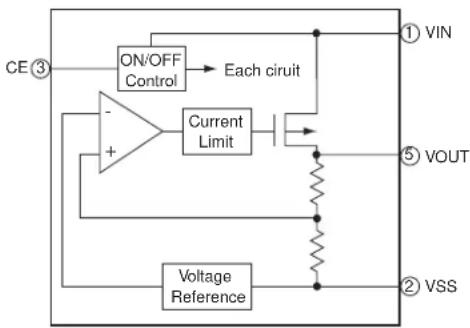
flowchart
graph TD
    CE["CE③"] -->|ON/OFF Control| A["Current Limit"]
    A --> B["Voltage Reference"]
    A --> C["VOUT"]
    A --> D["VSS"]
    E["① VIN"] --> F["Current Limit"]
    G["⑤ VOUT"] --> H["Current Limit"]
    I["② VSS"] --> J["Current Limit"]
    K["Ground"] --> A
    style CE fill:#f9f,stroke:#333
    style E fill:#ccf,stroke:#333
    style G fill:#ccf,stroke:#333
    style I fill:#ccf,stroke:#333
    style K fill:#cfc,stroke:#333
■ IC506 RUNTZA005AFZZL (UGNZ2): BLUETOOTH MODULE
| Pin No. | Terminal name | Input/ Output | Description of terminal |
| 1* | USBP | Input/ Output | USB DATA+ (Not used) |
| 2* | USBN | Input/ Output | USB DATA- (Not used) |
| 3 | UART_RTS Output | UART/Ready to send to DTE | |
| 4 | GND | — | Ground |
| 5 | GND | — | Ground |
| 6 | UART_TxD | Output | UART/TxD to DTE |
| 7 | UART_RxD | Input UART/RxD from DTE | |
| 8 | UART_CTS Input UART/Clear to send from DTE | ||
| 9 | PIO8 | Input/ Output | General purpose I/O |
| 10 | VCC_IO | Input Positive supply voltage for IO voltage Connect the VCC, if IO voltage is same as VCC | |
| 11 | VCC | Input Main supply voltage input 1 Regulated DC source recommended | |
| 12 | PCM_OUT Output PCM data stream output | ||
| 13 | PCM_SYNC Input/ Output | Connection to PCM frame sync Input/ output of 8 kHz | |
| 14* | XTAL_IN | Input Ext clock in (Not used) | |
| 15* | XTAL_OUT | Input Ext clock out (Not used) | |
| 16 | RESETB | Input System reset | |
| 17 | VDD18V | Output | VDD_CORE decupling capacitor |
| 18 | PCMCLK | Input/ Output | Connection to PCM reference Clock input/output of 256 kHz |
| 19 | PCM_IN | Input PCM data stream input | |
| 20 | PIO5 | Input/ Output | General purpose I/O |
CONFIDENTIAL
| Pin No. | Terminal name | Input/ Output | Description of terminal |
| 21 P | IO6 Input/ | Output | General purpose I/O |
| 22 P | IO3 Input/ | Output | General purpose I/O |
| 23 G | ND | — | Ground |
| 24 S | SPIMOSI Input/ | Output | For factory use only |
| 25 S | PICLK Input/ | Output | For factory use only |
| 26 P | IO4 Input/ | Output | General purpose I/O |
| 27 P | IO7 Input/ | Output | General purpose I/O |
| 28 P | IO1 Input/ | Output | General purpose I/O |
| 29 R | F_IO Input/ | Output | RF input/output |
| 30 G | ND | — | Ground |
| 31 S | SPIMISO Input/ | Output | For factory use only |
| 32* S | PICSB Input/ | Output | For factory use only (Not used) |
| 33 P | IO2 Input/ | Output | General purpose I/O |
| 34 P | IO0 Input/ | Output | General purpose I/O |
In this unit, the terminal withasterisk mark (*) is (open) terminal which is not connected to the outside.
■ IC507 VHITC7SET00FU- (TC7SET00FU): LOGIC
| Pin No. | Terminal name | Input/ Output | Description of terminal |
| 1 INB | Input Input B | ||
| 2 INA | Input Input A | ||
| 3 | GND | — | Ground |
| 4 OUT | Y Output | Output | Y |
| 5 | VCC | — | Power supply |
text_image
VCC 5 OUTY 4 (TOP VIEW) 1 2 3 IN B IN A GND■ IC508 VHI817A30NB-1R (817A30NB): 3.0V REGULATOR
| Pin No. | Terminal name | Input/ Output | Description of terminal |
| 1 | VSS | — | Ground (GND) |
| 2 VIN | Input Input voltage (VDD) | ||
| 3 VOUT | Output Output voltage | ||
| 4 | NC | — | Not used (CE) |

text_image
VIN ② VSS ① VOUT ③ Reference voltage Short-circuit protection circuit NC ④■ IC509 VHILVC2G34P-1R (LVC2G34P): BUFFER
| Pin No. | Terminal name | Input/ Output | Description of terminal |
| 1 1A | Input Input | ||
| 2 | GND | — | Ground |
| 3 2A | Input Input | ||
| 4 2Y | Output Output | ||
| 5 | VCC | — | Power supply |
| 6 1Y | Output Output |
text_image
1A 1 → ▶ 6 1Y 2A 3 → ▶ 4 2Y GND 2 5 VCC■ IC701 VHIR116025B-1L (R116025B): 2.5V REGULATOR
| Pin No. | Terminal name | Input/ Output | Description of terminal |
| 1 | VDD | Input | Input |
| 2 | GND | — | Ground |
| 3 | CE | Input | Chip enable |
| 4 | ECO | Input | High speed/low consumption selector switch |
| 5 | VOUT | Output | Output |
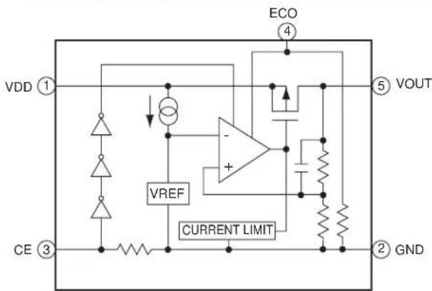
text_image
VDD ① CE ③ VREF CURRENT LIMIT ECO ④ ⑤ VOUT ② GNDCONFIDENTIAL
■ IC702 VHITK11131C-1R (TK11131C): REGULATOR
| Pin No. | Terminal name | Input/ Output | Description of terminal |
| 1 | CONT Input | Control | |
| 2 | GND | — | Ground |
| 3 | NP Input Capacitor (Vref) | ||
| 4 | VOUT Output | Output | |
| 5 | VIN Input Input | ||
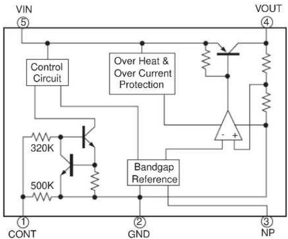
text_image
VIN ⑤ Control Circuit Over Heat & Over Current Protection 320K 500K Bandgap Reference VOUT ④ - + - CONT GND NP■ IC704 (LR38863): DISPLAY CONTROLLER
| Pin No. | Terminal name | Input/ Output | Description of terminal |
| 1 DUMMY4 | — | Dummy 4 | |
| 2 VDDPLL | — | PLL Power supply 1.8 V (1.6 V~ 2.0 V) | |
| 3 PLLGND | — | PLL Ground | |
| 4 PLLDIV0 Input PLL multiply switching signal | |||
| 5 PLLDIV1 Input PLL multiply switching signal | |||
| 6 HSD0 Input/ | Output | Data bus for high-speed serial transfer | |
| 7 HSD1 Input/ | Output | Data bus for high-speed serial transfer | |
| 8 HSD2 Input/ | Output | Data bus for high-speed serial transfer | |
| 9 HSWRD Input/ | Output | Read/Write determination signal for high-speed serial transfer | |
| 10 | HSEN | Input/ Output | High-speed serial data effective signal High is active |
| 11 | HSCK | Input/ Output | Standard clock for high-speed serial transfer (5 to 33 MHz) |
| 12 | DUMMY3 | — | Dummy 3 |
| 13 | PWM1/PORT8 | Output | PWM output 1 General-purpose PORT output (default) (Not used) |
| 14 | PLLDIV2 Input PLL multiply switching signal | ||
| 15 | VDDCORE | — | CORE Power supply 1.8 V (1.6 V~ 2.0 V) |
| 16 | GND | — | Logic ground |
| 17 | SUBWR_B | Input/ Output | Light signal for External display |
| Pin No. | Terminal name | Input/ Output | Description of terminal |
| 18 GND | — | Logic ground | |
| 19 VDDCORE | — | CORE Power supply 1.8 V (1.6 V~2.0 V) | |
| 20 PWM0/PORT3 Output PWM output 0 General-purpose PORT output (default) | |||
| 21 SUBCS_B | Input/ Output | Chip select signal for External display | |
| 22 CS_B | Input/ Output | Device select signal (Display is active when CS_B is "Low") | |
| 23 VDDIO | — | IO Power supply 3.0 V (2.7 V~3.3 V) | |
| 24 LCDINT Output External interrupt signal (Starting varies when interruption occurs.) | |||
| 25 GTDIO_B | Output | MPEG4ASIC internal core power-cut signal ("Low" is active.) | |
| 26 VDDIO | — | IO Power supply 3.0 V (2.7 V~3.3 V) | |
| 27 SUBDB1 | Input/ Output | Data bus for External display | |
| 28 BDATA[5] (B5) | Output D | splay panel B output signa | |
| 29 BDATA[5] (B4) | Output D | splay panel B output signa | |
| 30 BDATA[5] (B3) | Output D | splay panel B output signa | |
| 31 GND | — | Logic ground | |
| 32 TESTI | Input Test | terminal (Connected to GND normally) | |
| 33 BSHS_B | Input/ Output | External Bit Stream horizontal synchronization signal ("Low" is active) | |
| 34 WR_B | Input/ Output | Host write strobe signal | |
| 35 SUBRS | Input/ Output | Data determination signal for External display | |
| 36 MP4 RESET_B | Output M | MPEG4ASIC reset control signal ("Low" is active) | |
| 37 HSD6 Input/ | Output | Data bus for high-speed serial transfer | |
| 38 BDATA[2] (B2) | Output D | splay panel B output signal | |
| 39 BDATA[2] (B1) | Output D | splay panel B output signal | |
| 40 BDATA[2] (B0) | Output D | splay panel B output signal | |
| 41*EXCS_B1 | Input/ Output | Chip select output 1 (internal decode output) (Not used) | |
| 42*XOUT | Output O | scillation circuit output (Not used) | |
| 43 VDDIO | — | IO Power supply 3.0 V (2.7 V~3.3 V) | |
| 44 GND | — | Logic ground | |
| 45 SCANEN | Input | Full scan effective signal "High" is active (Connected to GND normally) | |
| 46 RD_B | Input/ Output | Host read strobe signal | |
| 47 RSP | Input/ Output | Register selection signalHOST_IF section :RSP =Low...Display accessRSP = High...Control accessHyper_Serial section :RSP = Low...Control accesRSP = High...Display access | |
| 48 GND | — | Logic ground | |
| 49 HSD3 Input/ | Output | Data bus for high-speed serial transfer | |
| 50 DCLK | Input/ Output | Data sampling clock (display clock) | |
CONFIDENTIAL
| Pin No. | Terminal name | Input/Output | Description of terminal |
| 51 V | SYNC Input/ | Output | Vertical synchronization signal |
| 52 H | SYNC Input/ | Output | Horizontal synchronization signal |
| 53* | XCS_B3 Input/ | Output | Chip select output 3 (internal decode output) (Not used) |
| 54 X | N Input Oscillation | circuit input | input/External clock input signal Clock input for full scan |
| 55 S | UBDB6 Input/ | Output | Data bus for External display |
| 56 R | RESET_B Input Master reset | (All registers are initialized when Low is activated) | |
| 57 S | UBDB0 Input/ | Output | Data bus for External display |
| 58 S | UBDB2 Input/ | Output | Data bus for External display |
| 59 H | SD5 Input/ | Output | Data bus for high-speed serial transfer |
| 60 D | B0 Input/ | Output | Data bus |
| 61 H | SD4 Input/ | Output | Data bus for high-speed serial transfer |
| 62* | XCS_B2 Input/ | Output | Chip select output 2 (internal decode output) (Not used) |
| 63 G | DATA[5] (G5) | Output Display panel G output signal | |
| 64 G | DATA[4] (G4) | Output Display panel G output signal | |
| 65 G | DATA[3] (G3) | Output Display panel G output signal | |
| 66 S | UBDB3 Input/ | Output | Data bus for External display |
| 67 S | UBDB4 Input/ | Output | Data bus for External display |
| 68 H | SD7 Input/ | Output | Data bus for high-speed serial transfer |
| 69 D | B1 Input/ | Output | Data bus |
| 70 D | B2 Input/ | Output | Data bus |
| 71 D | B3 Input/ | Output | Data bus |
| 72 D | B4 Input/ | Output | Data bus |
| 73 S | TKCHK Input Setting BS-related output terminal to Hi-z when a stack is installed (Connected to GND normally) | ||
| 74 V | DDCORE | — | CORE Power supply 1.8 V (1.6 V~ 2.0 V) |
| 75 GND | — | Logic ground | |
| 76 V | DDIO | — | IO Power supply 3.0 V (2.7 V~ 3.3 V) |
| 77 G | DATA[2] (G2) | Output Display panel G output signal | |
| 78 S | UBDB5 Input/ | Output | Data bus for External display |
| 79 B | SCLK Input/ | Output | External Bit Stream data clock |
| 80 S | UBCK Output Clock for External display | ||
| 81 D | B5 Input/ | Output | Data bus |
| 82 V | DDIO | — | IO Power supply 3.0 V (2.7 V~ 3.3 V) |
| 83 GND | — | Logic ground | |
| Pin No. | Terminal name | Input/Output | Description of terminal |
| 84 V | DDCORE | — | CORE Power supply 1.8 V (1.6 V~2.0 V) |
| 85 C | AMCK | Output Clock for camera operation | |
| 86 G | DATA[1] (G1) | Output Display panel G output signal | |
| 87 G | DATA[0] (G0) | Output Display panel G output signal | |
| 88 R | DATA[5] (R5) | Output Display panel R output signal | |
| 89 R | DATA[4] (R4) | Output Display panel R output signal | |
| 90 V | DDCORE | — | CORE Power supply 1.8 V (1.6 V~2.0 V) |
| 91* | PWMLCD/PORT4 | Output | PWM LCD output General-purpose PORT output (default) (Not used) |
| 92 B | SBLK_B Input/ | Output | External Bit Stream data effective signal ("High" is active when transferring the data) |
| 93 D | B6 Input/ | Output | Data bus |
| 94 D | B7 Input/ | Output | Data bus |
| 95 D | B8 Input/ | Output | Data bus |
| 96 D | B9 Input/ | Output | Data bus |
| 97 V | DDIO | — | IO Power supply 3.0 V (2.7 V~3.3 V) |
| 98 R | DATA[3] (R3) | Output Display panel R output signal | |
| 99 R | DATA[2] (R2) | Output Display panel R output signal | |
| 100 | RDATA[1] (R1) | Output Display panel R output signal | |
| 101 | RDATA[0] (R0) | Output Display panel R output signal | |
| 102* | MP4_P0 | Output MPEG4 control | |
| 103* | EXCS_B0 Input/ | Output | Chip select output 0 (internal decode output) (Not used) |
| 104 | BSPIXEL7 | Input/Output | External Bit Stream data bus |
| 105 | BSVS_B | Input/Output | External Bit Stream vertical synchronization signal ("Low" is active) |
| 106 | DB10 | Input/Output | Data bus |
| 107 | DB11 | Input/Output | Data bus |
| 108 | DB12 | Input/Output | Data bus |
| 109* | MP4_PLLCK | Output | MPEG4ASIC clock 15.36 MHz/CPU supply XIN clock (Not used) |
| 110 | SUBDB7 Input/ | Output | Data bus for External display |
| 111 | GND | — | Logic ground |
| 112 | DA0 Input/ | Output | Address input for chip select decode |
| 113 | BSPIXEL0 | Input/Output | External Bit Stream data bus |
| 114 | DCS_B | Input | Chip select input dedicated for chip select decode |
| 115 | VDDIO | — | IO Power supply 3.0 V (2.7 V~3.3 V) |
| 116 | BSPIXEL6 | Input/Output | External Bit Stream data bus |
| 117 | SE_DO/PORT0 | Output | Data output for 4-wire serial IF (default)General-purpose PORT output |
| 118 | DB13 | Input/Output | Data bus |
CONFIDENTIAL
| Pin No. | Terminal name | Input/ Output | Description of terminal |
| 119 DB14 Input/ | Output | Data bus | |
| 120 DB15 Input/ | Output | Data bus | |
| 121 WAIT_B Output External wait signal ("Low" is active) | |||
| 122 SUBFLMIN Input Driver FLM signal input for External display | |||
| 123 SUBCKS Output Clock switching signal for External display | |||
| 124 DA1 Input/ | Output | Address input for chip select decode | |
| 125 BSPIXEL1 Input/ | Output | External Bit Stream data bus | |
| 126 BSPIXEL4 Input/ | Output | External Bit Stream data bus | |
| 127 GND | — | Logic ground | |
| 128 BSPIXEL5 Input/ | Output | External Bit Stream data bus | |
| 129 SE_CK/PORT1 Output Control clock for 4-wire serial IF (default) General-purpose PORT output | |||
| 130 SE_LD2/PORT5 Output Load signal 2 for 4-wire serial IF General-purpose PORT output (default) | |||
| 131 BUFOFF_B Input Buffer Gated switching signal for I/O through current prevention (High when Host_IF signal is activated) | |||
| 132 VDDIO | — | IO Power supply 3.0 V (2.7 V~ 3.3 V) | |
| 133 DUMMY2 | — | Dummy 2 | |
| 134* SE_LD3/PORT6 Output Load signal 3 for 4-wire serial IF General-purpose PORT output (default) (Not used) | |||
| 135 VDDIO | — | IO Power supply 3.0 V (2.7 V~ 3.3 V) | |
| 136 SUBLPIN | Input Driver LP input External display | ||
| 137 BSPIXEL2 Input/ | Output | External Bit Stream data bus | |
| 138 BSPIXEL3 Input/ | Output | External Bit Stream data bus | |
| 139 VDDCORE | — | CORE Power supply 1.8 V (1.6 V~ 2.0 V) | |
| 140 SE_DI/PORT7 Input/ | Output | 4-wire serial input (default) General-purpose PORT output | |
| 141 SE_LD1/PORT2 Output Load signal 1 for 4-wire serial IF (default) General-purpose PORT output | |||
| 142 GND | — | Logic ground | |
| 143 VDDCORE | — | CORE Power supply 1.8 V (1.6 V~ 2.0 V) | |
| 144 DUMMY1 | — | Dummy 1Dummy 4 | |
In this unit, the terminal with asteriskmark (*) is (open) terminal which is not connected to the outside.
CONFIDENTIAL

flowchart
graph TD
    A["Reset"] --> B["Halt Ctrl"]
    B --> C["PLL"]
    C --> D["Clock Generator"]
    D --> E["MasterClock (MCLK)"]
    D --> F["SubLCDTimingClock (TCLK)"]
    D --> G["SubLCDTimingClock (STCK) XIN clock"]
    D --> H["LowSpeedClock (LCLK)"]
    D --> I["PWMClock (PCLK)"]
    D --> J["MPEGClock (MPCLK)"]
    D --> K["CameraClock (CAMCK)"]
    E --> L["MasterClock (MCLK)"]
    F --> M["SubLCDTimingClock (TCLK)"]
    G --> N["SubLCDTimingClock (STCK) XIN clock"]
    H --> O["LowSpeedClock (LCLK)"]
    I --> P["PWMClock (PCLK)"]
    J --> Q["MPEGClock (MPCLK)"]
    K --> R["CameraClock (CAMCK)"]
    L --> S["MasterClock (MCLK)"]
    M --> T["SubLCDTimingClock (TCLK)"]
    N --> U["PWMClock (PCLK)"]
    O --> V["SubLCDTimingClock (STCK) XIN clock"]
    P --> W["PWMClock (PCLK)"]
    Q --> X["MPEGClock (MPCLK)"]
    R --> Y["CameraClock (CAMCK)"]
    S --> Z["MasterClock (MCLK)"]
    T --> AA["SubLCDTimingClock (TCLK)"]
    U --> AB["PWMClock (PCLK)"]
    V --> AC["MPEGClock (MPCLK)"]
    W --> AD["CameraClock (CAMCK)"]
    X --> AE["MPEGClock (MPCLK)"]
    Y --> AF["CameraClock (CAMCK)"]
    Z --> AG["MPEGClock (MPCLK)"]
    AA --> AH["CameraClock (CAMCK)"]
    AB --> AI["MPEGClock (MPCLK)"]
    AC --> AJ["CameraClock (CAMCK)"]
    AD --> AK["MPEGClock (MPCLK)"]
    AE --> AL["MPEGClock (MPCLK)"]
    AF --> AM["MPEGClock (MPCLK)"]
    AG --> AN["MPEGClock (MPCLK)"]
    AH --> AO["MPEGClock (MPCLK)"]
    AI --> AP["MPEGClock (MPCLK)"]
    AJ --> AQ["MPEGClock (MPCLK)"]
    AK --> AR["MPEGClock (MPCLK)"]
    AL --> AS["MPEGClock (MPCLK)"]
    AM --> AT["MPEGClock (MPCLK)"]
    AN --> AU["MPEGClock (MPCLK)"]
    AO --> AV["MPEGClock (MPCLK)"]
    AP --> AW["MPEGClock (MPCLK)"]
    AS --> AX["MPEGClock (MPCLK)"]
    AT --> AY["MPEGClock (MPCLK)"]
    AU --> AZ["MPEGClock (MPCLK)"]
    AV --> BA["MPEGClock (MPCLK)"]
    AW --> BB["MPEGClock (MPCLK)"]
    AX --> BC["MPEGClock (MPCLK)"]
    AY --> BD["MPEGlock"]
    AZ --> BE["MPEGlock"]
    BA --> BF["MPEGlock"]
    BB --> BG["MPEGlock"]
    BC --> BH["MPEGlock"]
    BD --> BI["4-wire SO/PO"]
    BE --> BJ["4-wire SO/PO"]
    BF --> BK["4-wire SO/PO"]
    BG --> BL["4-wire SO/PO"]
    BH --> BM["4-wire SO/PO"]
    BI --> BN["4-wire SO/PO"]
    BJ --> BO["4-wire SO/PO"]
    BK --> BP["4-wire SO/PO"]
    BL --> BQ["4-wire SO/PO"]
    BM --> BR["4-wire SO/PO"]
    BN --> BS["4-wire SO/PO"]
    BO --> BT["4-wire SO/PO"]
    BP --> BU["4-wire SO/PO"]
    BR --> BV["4-wire SO/PO"]
    BS --> BW["4-wire SO/PO"]
    BT --> BX["4-wire SO/PO"]
    BU --> BY["4-wire SO/PO"]
    BW --> BZ["4-wire SO/PO"]
    BX --> CA["4-wire SO/PO"]
    BY --> CB["4-wire SO/PO"]
    CA --> CC["4-wire SO/PO"]
    BW --> CD["4-wire SO/PO"]
    BX --> CE["4-wire SO/PO"]
    BY --> CF["4-wire SO/PO"]
CONFIDENTIAL
■ IC708 VHITK11130C-1R (TK11130C): REGULATOR
| Pin No. | Terminal name | Input/ Output | Description of terminal |
| 1 V | CONT Input | Control | |
| 2 | GND | — | Groun |
| 3 | NP | — | Capacitor (Vref) |
| 4 V | OUT Output | Output | |
| 5 VIN | Input Input |
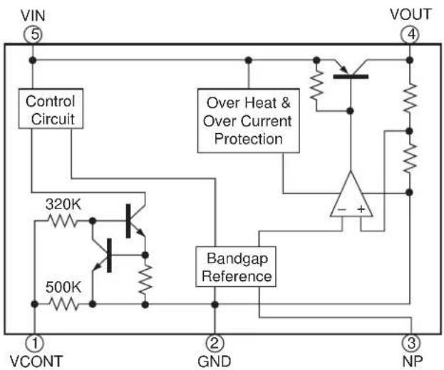
text_image
VIN ⑤ Control Circuit 320K 500K VCONT Over Heat & Over Current Protection Bandgap Reference VOUT ④ - + ② GND ③ NP■ IC801 VHIHD155155-1L(HD155155NP): RF
| Pin No. | Terminal name | Input/ Output | Description of terminal |
| 1 V | CCLNA Input VCC | for LNA transistor and LNA Bias | |
| 2 | P C S G | N—D | GND for Emitter of LNA transistor (PCS) |
| 3 P | CSLNAI Input | Positive input for LNA transistor (PCS) | |
| 4 P | CSLNAIB Input | Negative input for LNA transistor (PCS) | |
| 5 P | CSDCSGND | — | GND for Emitter of LNA transistor (PCS,DCS) |
| 6 D | CSLNAI | Input | Positive input for LNA transistor (DCS) |
| 7 D | CSLNAIB | Input | Negative input for LNA transistor (DCS) |
| 8 D | CSGSMGND | — | GND for Emitter of LNA transistor (DCS,GSM) |
| 9 G | SMLNAI | Input | Positive input for LNA transistor (GSM) |
| 10 | GSMLNAIB | Input | Negative input for LNA transistor (GSM) |
| 11 | GSMGND | — | GND for Emitter of LNA transistor (GSM) |
| 12 | PLLOUT | Output | Current output to control and modulate TXVCO |
| 13 | VCCOPLL | Input VCC for OPLL and Phase comparator | |
| 14 | VCCTXVCO | VCC for TXVCO | |
| 15 | GNDTXVCOD | — | GND for DCS/PCS TxVCO |
| 16 | GNDTXVCODB | — | GND for DCS/PCS TxVCO |
| 17 | TXOUTG | Output | Tx output for GSM |
| 18 | COMMONGND | GND for common | |
| 19 | TXOUTD | Output | Tx output for DCS/PCS |
| 20 | TXVCOGB | Input Negative TxVCO output for GSM | |
| 21 | TXVCOG | Input Positive TxVCO output for GSM | |
| 22 | VCCIQ | Input VCC for IQ modulator | |
| 23 | IOUT/IIN Input/ | Output | Positive output/input of I channel/modulator |
| Pin No. | Terminal name | Input/ Output | Description of terminal |
| 24 | IOUTB/IINB | Input/ Output | Negative output/input of I channel/modulator |
| 25 | QOUT/QIN | Input/ Output | Positive output/input of Q channel/modulator |
| 26 | QOUTB/QIN | Input/ Output | Negative output/input of Q channel/modulator |
| 27 | VCCIFSYN | Input | VCC for IFVCO Buffer and Divider, and IF Synthesiser |
| 28 | CPIFSYN | Output | Charge Pump output of IF Synthesiser |
| 29 | LE | Input Load enable for serial data | |
| 30 | CLK | Input Clock for serial data | |
| 31 | VCXOOUT | Output | Output for VCXO |
| 32 | SDATA | Input Serial Data | |
| 33* | GNDVCXO | — | GND for VCXO (Not used) |
| 34* | VCXOE | — | Emitter of VCXO transistor (Not used) |
| 35 | VCXOB | Input Base of VCXO transistor | |
| 36 | VCCVCXO Input | VCC for VCXO | |
| 37 | VCCRFSYN | Input VCC for RF Synthesiser | |
| 38 | CPRFSYN | Output | Charge Pump output of RF Synthesise |
| 39 | FLOCK | Output | FLOCK,Output,Fast Lock control for RF Synthesiser |
| 40 | VCCBB | Input VCC for Base band and State Logic | |
| 41 | VCCRFVCO Input | VCC for RF VCO | |
| 42 | DIVON | Output | VCXOOUT divider control input |
| 43 | VCCRFLO | Input VCC for RF Local Buffer and Divider | |
| 44 | CAPQB | Output | Capacitor for Q channel LPF (Negative output) |
| 45 | CAPQ | Output | Capacitor for Q channel LPF (Positive output) |
| 46 | CAPIB | Output | Capacitor for I channel LPF (Negative output) |
| 47 | CAPI | Output | Capacitor for I channel LPF (Positive output) |
| 48 | VCCMIX | Input VCC for Direct conversion Mixer | |
| 49 | GNDLNA | — | GND for LNA Bias |
In this unit, the terminal with asterisk mark (*) is (open) terminal which is not connected to the outside.
CONFIDENTIAL
IC802 RF3146
| Pin No. | Terminal name D | Description of terminal |
| 1 NC | Internal circuit node | Do not externally connect. |
| 2 VCC2 GSM | Controlled voltage input to the GSM driver stage. This voltage is part of the power control function for the module. This node must be connected to VCC OUT. This pin should be externally decoupled. | |
| 3 NC | Internal circuit node | Do not externally connect. |
| 4 GND | Internally connected to the package base. | |
| 5 GND | Internally connected to the package base. | |
| 6 GSM900 OUT RF output for the GSM bands. This is a 50Ω output. The output matching circuit and DC-block are internal to the package. | ||
| 7 GND | Internally connected to the package base. | |
| 8 NC | Internal circuit node. Do not externally connect. | |
| 9 NC | Internal circuit node. Do not externally connect. | |
| 10 NC | Internal circuit node. Do not externally connect. | |
| 11 NC | Internal circuit node. Do not externally connect. | |
| 12 NC | Internal circuit node. Do not externally connect. | |
| 13 NC | No internal or external connection. | |
| 14 NC | Internal circuit node. Do not externally connect. | |
| 15 NC | Internal circuit node. Do not externally connect. | |
| 16 NC | Internal circuit node. Do not externally connect. | |
| 17 NC | Internal circuit node. Do not externally connect. | |
| 18 VCC3 GSM Controlled voltage input to the GSM output stage. This voltage is part of the power control function for the module. This node must be connected to VCC OUT. This pin should be externally decoupled. | ||
| 19 VCC OUT Controlled voltage output to feed VCC2 and VCC3. This voltage is part of the power control function for the module. It cannot be connected to any pins other than VCC2 and VCC3. | ||
| 20 VCC OUT Controlled voltage output to feed VCC2 and VCC3. This voltage is part of the power control function for the module. It cannot be connected to any pins other than VCC2 and VCC3. | ||
| 21 VCC3 DCS/PCS Controlled voltage input to the DCS/PCS output stage. This voltage is part of the power control function for the module. This node must be connected to VCC OUT. This pin should be externally decoupled. | ||
| 22 NC | Internal circuit node. Do not externally connect. | |
| 23 NC | Internal circuit node. Do not externally connect. | |
| 24 NC | No internal or external connection. | |
| 25 NC | Internal circuit node. Do not externally connect. | |
| 26 NC | Internal circuit node. Do not externally connect. | |
| 27 NC | Internal circuit node. Do not externally connect. | |
| 28 NC | Internal circuit node. Do not externally connect. | |
| 29 NC | Internal circuit node. Do not externally connect. | |
| 30 GND | Internally connected to the package base. | |
| 31 DCS/PCS OUT RF output for the DCS/PCS bands. This is a 50Ω output. The output matching circuit and DC-block are internal to the package. | ||
| 32 GND | Internally connected to the package base. | |
| 33 NC | Internal circuit node. Do not externally connect. | |
| 34 GND | Internally connected to the package base. | |
| 35 VCC2 DCS/PCS Controlled voltage input to the DCS/PCS driver stage. This voltage is part of the power control function for the module. This node must be connected to VCC OUT. This pin should be externally decoupled. | ||
| Pin No. | Terminal name D | Description of terminal |
| 36 NC | No internal connection. | Connect to ground plane close to the package pin. |
| 37 DCS/PCS IN RF input | for the DCS/PCS band.This is a 50Ω output. | |
| 38 NC | No internal connection. | Connect to ground plane close to the package pin. |
| 39 VCC1 | DCS/PCS Controlled voltage input to the DCS/PCS driver stage. This voltage is applied internal to the package. This pin should be externally decoupled. | |
| 40 BAND SEL | A | lows external control to select the GSM or DSC/PCS bands with a logic high or low. A logic low enables the GSM bands, whereas a logic high enables the DCS/PCS bands. |
| 41 TX | ENABLE | This signal enables the PA module for operation with a logic high. Both bands are disabled with a logic low. |
| 42 VBATT | Power supply for the module. This pin should be externally decoupled and connected to the battery. | |
| 43 VBATT | Power supply for the module. This pin should be externally decoupled and connected to the battery. | |
| 44 NC | Internal circuit node. Do not externally connect. | |
| 45 VRAMP | Ramping signal from DAC. A simple RC filter may be required depending on the selected baseband. | |
| 46 VCC1 GSM | Internally connected to VCC1 (pin39).No external connection required. | |
| 47 GND1 GSM | Ground connection for the GSM preamplifier stage. Connect to ground plane close to the package pin. | |
| 48 | GSM900 IN | RF input to the GSM band. This is a 50Ω input. |
| Pkg base | GND Connect to ground plane with multiple via holes. See recommended footprint. | |

text_image
DCS/PCS IN 37 BAND SELECT 40 TX ENABLE 41 VBATT 42 VBATT 43 VRAMP 45 GSM IN 48 Fully Integrated Power Control Circuit DCS/PCS OUT 6 GSM OUT■ IC804 VHIR5322N29-1L(R5322N002B): POWER SUPPLY
| Pin No. | Terminal name | Input/ Output | Description of terminal |
| 1 CE1 | Input Chip Enable1 | ||
| 2 VDD | Input Power supply | ||
| 3 CE2 | Input Chip Enable2 | ||
| 4 VOUT2 | Output VCC for VRF | ||
| 5 GND | — | Ground | |
| 6 VOUT1 | Output VCC for VTCXO | ||

text_image
CE1 ① VDD ② CE2 ③ ⑥ VOUT ⑤ GND ④ VOUT2CONFIDENTIAL
[2] FUNCTION TABLE OF DISPLAY
■ LCD1000 RLCUB0048AF03: MAIN DISPLAY
| Pin No. | Terminal name | Input/Output | Description of terminal |
| 1 T | -COM Input | COM electric potential input for CS | |
| 2 T | -COM Input | COM electric potential input for CS | |
| 3 T | FT-COM Input | COM voltage input | |
| 4 | COMC Output | COM signal output | |
| 5 | COMC Output | COM signal output | |
| 6 | COMDC Output | COM center voltage output | |
| 7 | VCOMH Output | COM amplitude voltage output | |
| 8 | B0 Input Blue data signal (LSB) | ||
| 9 | B1 Input Blue data signal | ||
| 10 | B2 Input Blue data signal | ||
| 11 | B3 Input Blue data signal | ||
| 12 | B4 Input Blue data signal | ||
| 13 | B5 Input Blue data signal (MSB) | ||
| 14 | G0 Input Green data signal (LSB) | ||
| 15 | G1 Input Green data signal | ||
| 16 | G2 Input Green data signal | ||
| 17 | G3 Input Green data signal | ||
| 18 | G4 Input Green data signal | ||
| 19 | G5 Input Green data signal (MSB) | ||
| 20 | R0 Input Red data signal (LSB) | ||
| 21 | R1 Input Red data signal | ||
| 22 | R2 Input Red data signal | ||
| 23 | R3 Input Red data signal | ||
| 24 | R4 Input Red data signal | ||
| 25 | R5 Input Red data signal (MSB) | ||
| 26 | DCLK Input Data sampling clock | ||
| 27 | HSY | Input Horizontal sync signal | |
| 28 | VSY | Input Vertical sync signal | |
| 29 | SO | Output serial data output | |
| 30 | SI | Input serial data input | |
| 31 | SCLK | Input serial clock input | |
| 32 | CS | Input serial interface chip select | |
| 33 | RESET | Input Hardware reset | |
| 34 | VCC | — | Logic power |
| 35 | GND | — | Ground |
| 36 | GND | — | Ground |
| 37 | VDC | — | Analog power |
| 38 | VDC | — | Analog power |
| 39 | COM2 | — | COM control for CS |
| 40 | VCLAMP Output Voltage for CS output | ||
| 41 | VSS2 | Output DC/DC converter output | |
| 42 | VSS1 | Output DC/DC converter output | |
| 43 | NC | — | Not used |
| 44 | VDD2 | Output DC/DC converter output | |
| 45 | C5- | — | Booster capacitor connection terminal |
| 46 | C5+ | — | Booster capacitor connection terminal |
| Pin No. | Terminal name | Input/ Output | Description of terminal |
| 47 | C4- | — | Booster capacitor connection terminal |
| 48 | C4+ | — | Booster capacitor connection terminal |
| 49 | C3- | — | Booster capacitor connection terminal |
| 50 | C3+ | — | Booster capacitor connection terminal |
| 51 | C2- | — | Booster capacitor connection terminal |
| 52 | C2+ | — | Booster capacitor connection terminal |
| 53 | C1- | — | Booster capacitor connection terminal |
| 54 | C1+ | — | Booster capacitor connection terminal |
| 55 | VDC2 | Output DC/DC converter output | |
| 56 | VDC2 | Output DC/DC converter output | |
| 57 | VR | Output Reference power supply output | |
| 58 | VS | Output Source power supply output | |
| 59 | VS | Output Source power supply output | |
In this unit, the terminal with asterisk mark (*) is (open) terminal which is not connected to the outside.

text_image
MAIN DISPLAY To InputTerminal ① ⑤■ LCD001 RLCUB0049AFZZ : EXTERNAL DISPLAY
| Pin No. | Terminal name | Input/ Output | Description of terminal | Notes |
| 1 | V0 | — | Display drive power supply terminal | — |
| 2 | V1 | — | Display drive power supply terminal | — |
| 3 | V2 | — | Display drive power supply terminal | — |
| 4 | V3 | — | Display drive power supply terminal | — |
| 5 | V4 | — | Display drive power supply terminal | — |
| 6 | GND | — | Ground | — |
| 7 | RESB Input Reset signal | — | ||
| 8 | CSB Input Chip select signal | — | ||
| 9 | RS Input Register select signal "0": Display RAM data "1": Command data | |||
| 10 | WRB Input Write signal "L": Activated | |||
| 11 | RDB Input Read signal "L": Activated | |||
CONFIDENTIAL
| Pin No. | Terminal name | Input/ Output | Description of terminal | Notes |
| 12 D0 Input/ | Output | Data signal | — | |
| 13 D1 Input/ | Output | Data signal | — | |
| 14 D2 Input/ | Output | Data signal | — | |
| 15 D3 Input/ | Output | Data signal | — | |
| 16 D4 Input/ | Output | Data signal | — | |
| 17 D5 Input/ | Output | Data signal | — | |
| 18 D6 Input/ | Output | Data signal | — | |
| 19 D7 Input/ | Output | Data signal | — | |
| 20 LP Input/ | Output | Latch signal | — | |
| 21 FLM Output | Display sync signal | — | ||
| 22 GND (VSS) | — | Ground | — | |
| 23 CK Input Master clock | external input terminal | — | ||
| 24 CKS Input Master clock | selection terminal | "L": Built-in oscillation | ||
| 25 VDD/VEE | — | Logic system power supply terminal | — | |
| 26 VREG Output Output | terminal for generating constant voltage | — | ||
| 27 VOUT Output Built-in | step-up circuit output terminal | — | ||
| 28 CAP1 - | Output Booster capacitor connection terminal (-) | — | ||
| 29 CAP1+ Output Booster capacitor connection terminal (+) | — | |||
| 30 CAP2 - | Output Booster capacitor connection terminal (-) | — | ||
| 31 CAP2+ Output Booster capacitor connection terminal (+) | — | |||
| 32 CAP3 - | Output Booster capacitor connection terminal (-) | — | ||
| 33 CAP3+ Output Booster capacitor connection terminal (+) | — | |||
text_image
EXTERNAL DISPLAY ① ③ To Input TerminalSHARP
COPYRIGHT 2004 BY SHARP CORPORATION
All rights reserved.
Printed in Japan.
No part of this publication may be reproduced,
stored in a retrieval system, or transmitted.
In any form or by any means,
electronic, mechanical, photocopying, recording, or otherwise,
without prior written permission of the publisher.
SHARP CORPORATION
Information and Communication Systems Group
Products Quality Assurance Department
Yamatokoriyama, Nara 639-1186, Japan
2004 December Printed in Japan ⓣ