TA890FXE - Motherboard BIOSTAR - Free user manual and instructions
Find the device manual for free TA890FXE BIOSTAR in PDF.

User questions about TA890FXE BIOSTAR
0 question about this device. Answer the ones you know or ask your own.
Ask a new question about this device
Download the instructions for your Motherboard in PDF format for free! Find your manual TA890FXE - BIOSTAR and take your electronic device back in hand. On this page are published all the documents necessary for the use of your device. TA890FXE by BIOSTAR.
USER MANUAL TA890FXE BIOSTAR
FCC Information and Copyright
This equipment has been tested and found to comply with the limits of a Class B digital device, pursuant to Part 15 of the FCC Rules. These limits are designed to provide reasonable protection against harmful interference in a residential installation. This equipment generates, uses, and can radiate radio frequency energy and, if not installed and used in accordance with the instructions, may cause harmful interference to radio communications. There is no guarantee that interference will not occur in a particular installation.
The vendor makes no representations or warranties with respect to the contents here and specially disclaims any implied warranties of merchantability or fitness for any purpose. Further the vendor reserves the right to revise this publication and to make changes to the contents here without obligation to notify any party beforehand.
Duplication of this publication, in part or in whole, is not allowed without first obtaining the vendor's approval in writing.
The content of this user's manual is subject to be changed without notice and we will not be responsible for any mistakes found in this user's manual. All the brand and product names are trademarks of their respective companies.
Table of Contents
Chapter 1: Introduction ...... 1
1.1 Before You Start 1
1.2 Package Checklist....1
1.3 Motherboard Features....2
1.4 Rear Panel Connectors 3
1.5 Motherboard Layout....4
Chapter 2: Hardware Installation .... 5
2.1 Installing Central Processing Unit (CPU) 5
2.2 FAN Headers....7
2.3 Installing System Memory 8
2.4 Connectors and Slots 10
Chapter 3: Headers & Jumpers Setup .... 14
3.1 How to Setup Jumpers 14
3.2 Detail Settings 14
Chapter 4: Hybrid CrossFireX Function ...... 20
4.1 Hybrid CrossFireX Requirements 20
4.2 Hybrid CrossFireX Installation....20
Chapter 5: RAID Functions ...... 21
5.1 Operating System.... 21
5.2 Raid Arrays 21
5.3 How RAID Works 21
Chapter 6: T-Series BIOS & Software.... 25
6.1 T-Series BIOS 25
6.2 T-Series Software 33
Chapter 7: Useful Help 43
7.1 Driver Installation Note 43
7.2 Extra Information....44
7.3 AMI BIOS Beep Code 45
7.4 AMI BIOS Post Code 46
7.5 Conversion Of Hexadecimal and Decimal System.... 48
7.6 Troubleshooting....49
Appendix: SPEC In Other Languages 50
German....50
French 52
Italian....54
Spanish 56
Portuguese 58
Polish....60
Russian 62
Arabic....64
Japanese 66
CHAPTER 1: INTRODUCTION
1.1 B EFORE YOU START
Thank you for choosing our product. Before you start installing the motherboard, please make sure you follow the instructions below:
■ Prepare a dry and stable working environment with sufficient lighting.
■ Always disconnect the computer from power outlet before operation.
■ Before you take the motherboard out from anti-static bag, ground yourself properly by touching any safely grounded appliance, or use grounded wrist strap to remove the static charge.
■ Avoid touching the components on motherboard or the rear side of the board unless necessary. Hold the board on the edge, do not try to bend or flex the board.
■ Do not leave any unfastened small parts inside the case after installation. Loose parts will cause short circuits which may damage the equipment.
- Keep the computer from dangerous area, such as heat source, humid air and water.
■ The operating temperatures of the computer should be 0 to 45 degrees Celsius.
1.2 PACKAGE CHECKLIST
IDE Cable X1 (optional)
Serial ATA Cable X3
Serial ATA Power Cable X1
Rear I/O Panel for ATX Case X1
↓ User's Manual X1
+ Fully Setup Driver CD X1
FDD Cable X1 (optional)
USB 2.0 Cable X1 (optional)
S/PDIF out Cable X1 (optional)
CFX Bridge X2
Note: The package contents may be different due to area or your motherboard version.
1.3 MOTHERBOARD FEATURES
| SPEC | ||
| CPU | Socket AM3AMD Sempron / Phenom II / Athlon IIprocessors | AMD 64 Architecture enables 32 and 64 bit computingSupports Hyper Transport 3.0 |
| FSB | Support HyperTransport 3.0Supports up to 5.2 GT/s Bandwidth | |
| Chipset | AMD 890FXAMD SB850 | |
| Super I/O | ITE 8721Provides the most commonly used legacySuper I/O functionality.Low Pin Count Interface | Environment Control in itatives,H/W MonitorFan Speed ControllerITE's "Smart Guard Ian" function |
| MainMemory | DDR3 DIMM Slots x 4Max Memory Capacity 16GBEach DIMM supports 512MB/1GB/2GB/4GB DDR3 | Dual Channel Mode DDR3 memory modu leSupports DDR3 800 / 1066 / 1333Supports DDR3 1600 (OC) |
| IDE | VIA VT6330 | Ultra DMA 33 / 66 / 100 / 133 Bus Master Mode supports PIO Mode 0~4, |
| SATA III | Integrated Serial ATA Controller | Data transfer rates up to 6 Gb/s.SATA Version 3.0 spe of ic at ion co mp liant.RAID 0,1,5,10 support |
| LAN | Realtek RTL 8111DL | 10 / 100 Mb/s / 1Gb/s auto negotiationHalf / Full duplex capability |
| Sound | ALC892 | 7.1channels audio outSupports HD Audio |
| IEEE 1394 | VIA VT6330 1394a | |
| Slots | PCI Slot x2 Supports PCI expansion cardsPCI Express Gen2 x16 Slot x4 | Supports PCI-E Gen2 x16,x16, x4, x1 expansion cards |
| On BoardConnectors | IDE Connector x1 Each connector supports 2 IDE devicesSATA Connector x5 Each connector supports 1 SATA deviceFront Panel Connector x1 Supports front panel facilitiesFront Audio Connector x1 Supports front panel audio functionS/PDIF out Connector x1 Supports digital audio out functionConsumer IR Connector x1 Supports infrared functionCPU Fan Header x1 CPU Fan power supply (with Smart Fan function)System Fan Header x2 System Fan Power supplyCMOS clear Header x1 Restore CMOS data to factory defaultUSB Connector x3 Each connector supports 2 front panel USB portsIEEE 1394 Connector x1 Connects to IEEE 1394 deviceSerial Port Connector x1 Connects to RS-232 PortPower Connector (24-Pin) x1 Connects to Power supplyPower Connector (8-Pin) x1 Connects to Power supply | |
| Back Panel I/O | PS/2 Keyboard x1PS/2 Mouse x1Optical +coaxial S/PDIF Out x11394 Port x1eSATA Port x1LAN port x1USB Port x6Audio Jack x6 | Connects to PS/2 KeyboardConnects to PS/2 MouseProvides digital audio out functionConnects to IEEE 1394 deviceConnect to SATA devicesConnect to RJ-45 ethernet cableConnect to USB devicesProvide Audio-In/Out and Mic. connection |
| Board Size | 305 mm (W) x 244 mm (L) | ATX |
| OS Support | Windows XP / Vista / 7 | Biostar reserves the right to add or remove support for any OS With or without notice. |
1.4 REAR PANEL CONNECTORS
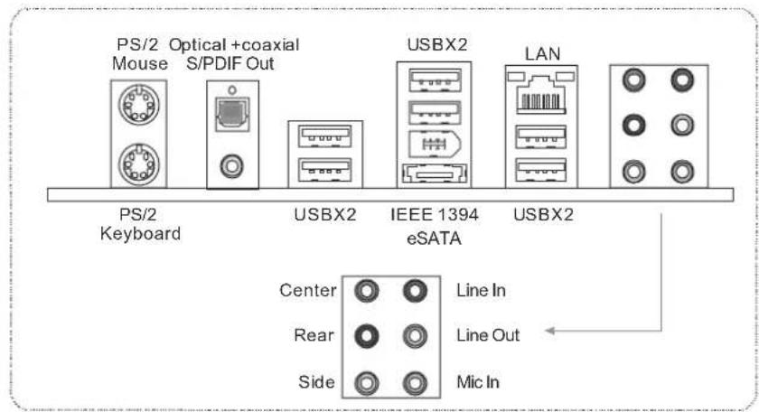
text_image
PS/2 Mouse Optical +coaxial S/PDIF Out PS/2 Keyboard USBX2 IEEE 1394 eSATA LAN Center Line In Rear Line Out Side Mic In1.5 MOTHERBOARD LAYOUT
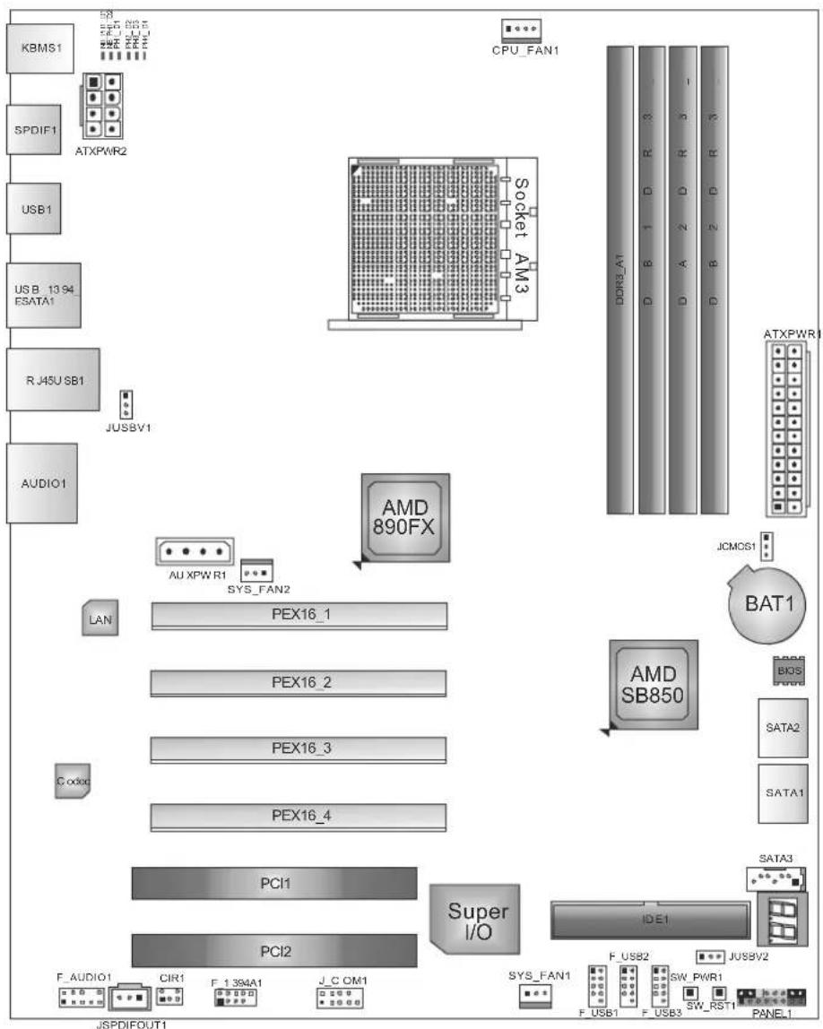
text_image
KBMS1 SPDIF1 ATXPWR2 USB1 USB B 13.94 ESATA1 R J45U SB1 JUSBV1 AUDIO1 CPU_FAN1 Socket AM3 AMD 890FX AU XPWR1 SYS_FAN2 LAN PEX16_1 PEX16_2 PEX16_3 C codio PEX16_4 PCI1 Super I/O F_AUDIO1 CIR1 F_1.39A1 J_C OM1 SYS_FAN1 F_USB2 JUSBV2 SW_PWR1 SW_RST1 PANEL_1 JSPDIFOUT1 DDR/EA1 ATXPWR1 JCMCS1 BAT1 AMD SB850 BOS SATA2 SATA1 IDE1Note: represents the 1 ^st pin.
CHAPTER 2: HARDWARE INSTALLATION
2.1 INSTALLING CENTRAL PROCESSING UNIT (CPU)
text_image
Diagram of a computer motherboard layout with labeled components and an arrow indicating direction or flow.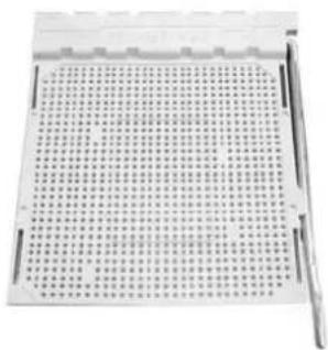
natural_image
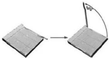
Close-up of a perforated metal plate with grid pattern and a small ruler at the bottom (no visible text or symbols)Step 1: Pull the lever toward direction A from the socket and then raise the lever up to a 90-degree angle.
natural_image
Diagram showing two rectangular blocks with a curved arrow labeled 90°, no text or symbols presentStep 2: Look for the white triangle on socket, and the gold triangle on CPU should point towards this white triangle. The CPU will fit only in the correct orientation.
natural_image
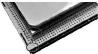
Close-up of a perforated metal panel with a small circular component inserted (no text or symbols visible)Step 3: Hold the CPU down firmly, and then close the lever toward direct B to complete the installation.
flowchart
graph TD
    A["AMD"] --> B["Standard AMD"]
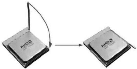
Step 4: Put the CPU Fan on the CPU and buckle it. Connect the CPU FAN power cable to the CPU_FAN1. This completes the installation.
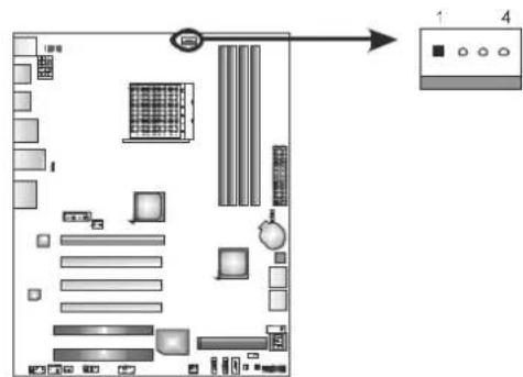
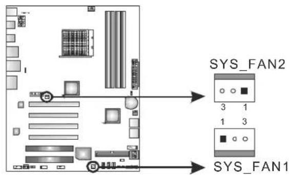
2.2 FAN HEADERS
These fan headers support cooling-fans built in the computer. The fan cable and connector may be different according to the fan manufacturer. Connect the fan cable to the connector while matching the black wire to pin#1.
CPU_FAN1: CPU Fan Header
text_image
Diagram of a computer motherboard layout with labeled components and directional arrowPin Assignment
1 Ground
2 +12V
3 FAN RPM rate sense
4 Smart Fan Control (By Fan)
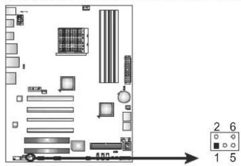
SYS_FAN1: System Fan Header
SYS_FAN2: NorthBridge Fan Header
text_image
SYS_FAN2 3 1 1 3 SYS_FAN1Pin Assignment
1 Ground
2 +12V
3 FAN RPM rate sense
Note:
CPU_FAN1, SYS_FAN1/2 support 4-pin and 3-pin head connectors. When connecting with wires onto connectors, please note that the red wire is the positive and should be connected to pin#2, and the black wire is Ground and should be connected to GND.
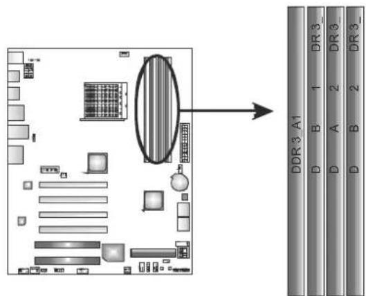
2.3 INSTALLING SYSTEM MEMORY
A. DDR3 Modules
flowchart
graph TD
    A["CPU socket"] --> B["Monitor"]
    B --> C["Memory Unit"]
    C --> D["DDR 3_A1 Interface"]
    style A fill:#f9f,stroke:#333
    style B fill:#ccf,stroke:#333
    style C fill:#cfc,stroke:#333
    style D fill:#fcc,stroke:#333
- Unlock a DIMM slot by pressing the retaining clips outward. Align a DIMM on the slot such that the notch on the DIMM matches the break on the Slot.
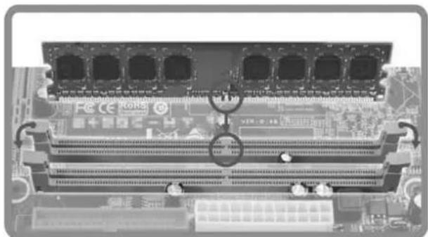
natural_image
Close-up of a computer RAM module with multiple slots and ventilation slots, no visible text or symbols- Insert the DIMM vertically and firmly into the slot until the retaining chip snap back in place and the DIMM is properly seated.
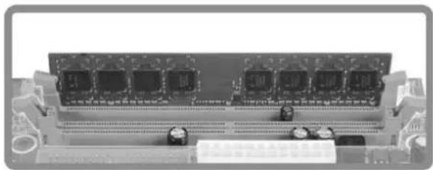
natural_image
Front view of a computer RAM module with multiple drive bays and connectors (no visible text or labels)B. Memory Capacity
| DIMM Socket Location | DDR3 Module | Total Memory Size |
| DDR3_A1 | 512MB/1GB/2GB/4GB | Max is 16GB. |
| DDR3_B1 | 512MB/1GB/2GB/4GB | |
| DDR3_A2 | 512MB/1GB/2GB/4GB | |
| DDR3_B2 | 512MB/1GB/2GB/4GB |
C. Dual Channel Memory installation
Please refer to the following requirements to activate Dual Channel function:
Install memory module of the same density in pairs, shown in the table.
| Dual Channel Status | DDR3_A1 | DDR3_B1 | DDR3_A2 | DDR3_B2 |
| Enabled | O | O | X | |
| Enabled | X | X | O | |
| Enabled | O | O | O |
(O: memory installed; X: memory not installed)
The DRAM bus width of the memory module must be the same (x8 or x16)
2.4 CONNECTORS AND SLOTS
IDE1: IDE/ATAPI Connector
The motherboard has a 32-bit Enhanced IDE Controller that provides PIO Mode 0\~4, Bus Master, and Ultra DMA 33/66/100/133 functionality.
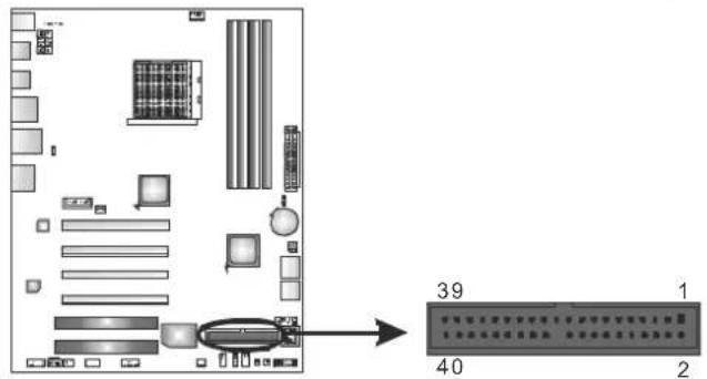
text_image
Diagram of a computer motherboard layout with labeled components and a connector pin layout showing 39, 40, and 1 pins.SATA1\~SATA3: Serial ATA Connectors
The motherboard has a PCI to SATA Controller with 5 channels SATA interface, it satisfies the SATA 3.0 spec and with transfer rate of 6.0Gb/s.
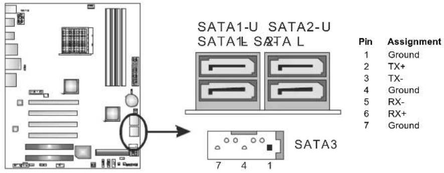
text_image
SATA1-U SATA2-U SATA1L SATA L Pin Assignment 1 Ground 2 TX+ 3 TX- 4 Ground 5 RX- 6 RX+ 7 Ground SATA3 7 4 1ATXPWR1: ATX Power Source Connector
This connector allows user to connect 24-pin power connector on the ATX power supply.
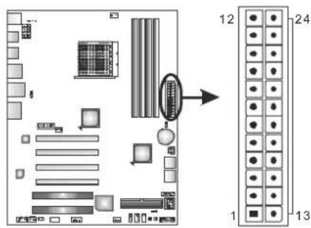
text_image
Diagram of a computer motherboard layout with labeled pins and connectors, showing connections to a 12-pin connector and numbered parts.| Pin | Assignment | Pin | Assignment | |
| 13 | +3.3V | 1 | +3.3V | |
| 14 | -12V | 2 | +3.3V | |
| 15 | Ground | 3 | Ground | |
| 16 | PS_ON | 4 | +5V | |
| 17 | Ground | 5 | Ground | |
| 18 | Ground | 6 | +5V | |
| 19 | Ground | 7 | Ground | |
| 20 | NC | 8 | PW_OK | |
| 21 | +5V | 9 | Standby Voltage+5V | |
| 22 | +5V | 10 | +12V | |
| 23 | +5V | 11 | +12V | |
| 24 | Ground | 12 | +3.3V | |
ATXPWR2: AT X Power Source Connector
This connector provides +12V to CPU power circuit.
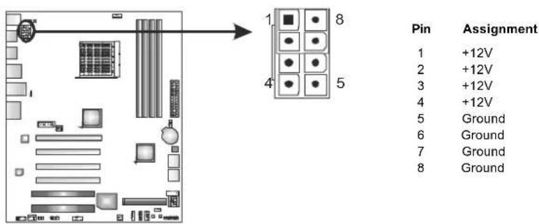
text_image
Pin Assignment 1 +12V 2 +12V 3 +12V 4 +12V 5 Ground 6 Ground 7 Ground 8 GroundNote:
Before you power on the system, please make sure that both ATXPWR1 and ATXPWR2 connectors have been plugged-in.
If CPU power plug is 4-pin, please plug it into Pin 1-2-5-6 of ATXPWR2.
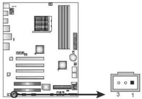
AUXPWR1: Auxiliary Power for Graphics
This connector is an auxiliary power connection for graphics cards. Exclusive power for the graphics card provides better graphics performance.
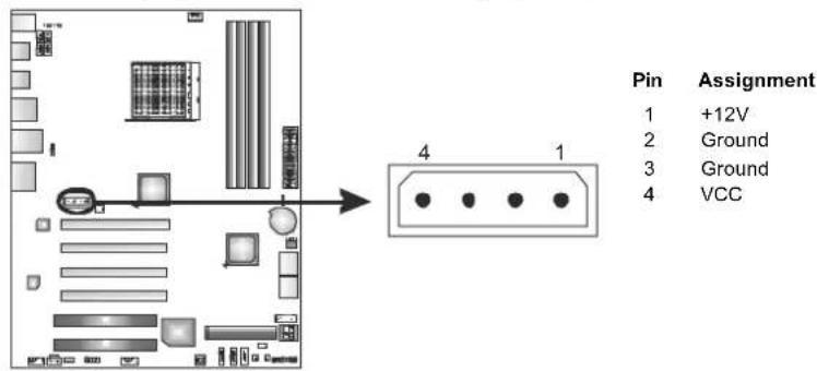
text_image
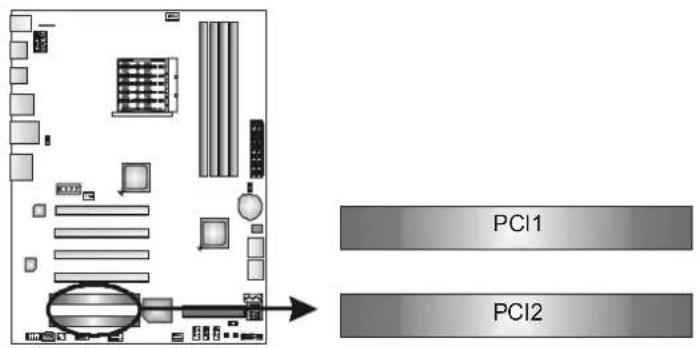
Pin Assignment 1 +12V 2 Ground 3 Ground 4 VCCPCI1/PCI2: Peripheral Component Interconnect Slots
This motherboard is equipped with 2 standard PCI slots. PCI stands for Peripheral Component Interconnect, and it is a bus standard for expansion cards. This PCI slot is designated as 32 bits.
text_image
PCI1 PCI2PEX16\_1/PEX16\_3: PCI-Express Gen2 x16 Slots
- PCI-Express 2.0 compliant.
- Maximum theoretical realized bandwidth of 8GB/s simultaneously per direction, for an aggregate of 16GB/s totally.
- PCI-Express Gen2 supports a raw bit-rate of 5.0Gb/s on the data pins.
- PEX16_1 & PEX16_3 slots are reserved for graphic or video cards.
PEX16\_4: PCI-Express Gen2 x4 Slot
- PCI-Express 2.0 compliant.
- Maximum theoretical realized bandwidth of 2GB/s simultaneously per direction, for an aggregate of 4GB/s totally.
PEX16\_2: PCI-Express Gen2 x1 Slot
- PCI-Express 2.0 compliant.
- Data transfer bandwidth up to 250MB/s per direction; 500MB/s in total.
- PCI-Express supports a raw bit-rate of 2.5Gb/s on the data pins.
text_image
Floor plan diagram with labeled rooms and directional arrow indicating layout or movementPEX16 1
PEX16_2
PEX16 3
PEX16 4
CHAPTER 3: HEADERS & JUMPERS SETUP
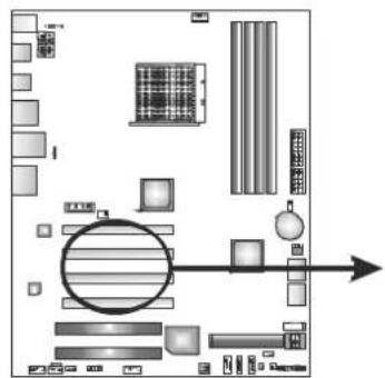
3.1 HOW TO SETUP JUMPERS
The illustration shows how to set up jumpers. When the jumper cap is placed on pins, the jumper is "close", if not, that means the jumper is "open".
Pin1-2
closed
3.2 DETAIL SETTINGS
PANEL1: Front Panel Header
This 16-pin connector includes Power-on, Reset, HDD LED, Power LED, and speaker connection. It allows user to connect the PC case's front panel switch functions.
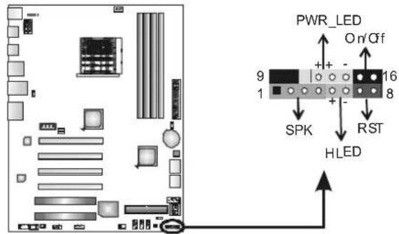
text_image
PWR_LED On/Off 9 16 8 SPK RST HLED| Pin | Assignment | Function | Pin | Assignment | Function |
| 1 | +5V | Speaker Connector | 9 | N/A | N/A |
| 2 | N/A | 10 | N/A | ||
| 3 | N/A | 11 | N/A | N/A | |
| 4 | Speaker | 12 | Power LED (+) | Power LED | |
| 5 | HDD LED (+) | Hard drive LED | 13 | Power LED (+) | |
| 6 | HDD LED (-) | 14 | Power LED (-) | ||
| 7 | Ground | Reset button | 15 | Power button | Power-on button |
| 8 | Reset control | 16 | Ground |
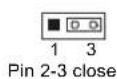
JCMOS1: Clear CMOS Header
Placing the jumper on pin2-3 allows user to restore the BIOS safe setting and the CMOS data. Please carefully follow the procedures to avoid damaging the motherboard.
text_image
Diagram of a computer motherboard layout with labeled components and directional arrow indicating assembly or connection.
Pin 1-2 Close: Normal Operation (default).

Pin 2-3 Close: Clear CMOS data.
- Remove AC power line.
- Set the jumper to "Pin 2-3 close".
- Wait for five seconds.
- Set the jumper to "Pin 1-2 close".
- Power on the AC.
- Reset your desired password or clear the CMOS data.
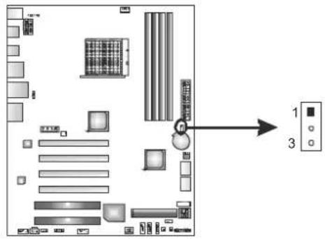
J\_COM1: Serial port Connector
The motherboard has a Serial Port Connector for connecting RS-232 Port.
text_image
Diagram of a computer motherboard layout with labeled components and a numbered indicator box for ports 1, 2, and 9.Pin Assignment
1 Carrier detect
2 Received data
3 Transmitted data
4 Data terminal ready
5 Signal ground
6 Data set ready
7 Request to send
8 Clear to send
9 Ring indicator
10 NC
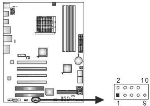
F AUDIO1: Front Panel Audio Header
This header allows user to connect the front audio output cable with the PC front panel. This header allows only HD audio front panel connector; AC'97 connector is not acceptable.
text_image
Diagram of a computer motherboard layout with labeled components and a numbered indicator box for ports 1, 2, and 9.Pin Assignment
1 Mic Left in
2 Ground
3 Mic Right in
4 GPIO
5 Right line in
6 Jack Sense
7 Front Sense
8 Key
9 Left line in
10 Jack Sense
JSPDIFOUT1: Digital Audio-out Connector
This connector allows user to connect the PCI bracket SPDIF output header.
text_image
Diagram of a computer motherboard layout with labeled components and directional arrow indicating orientationPin Assignment
1 +5V
2 SPDIF_OUT
3 Ground
CIR1: Consumer IR Connector
This header is for infrared remote control and communication.
text_image
Floor plan diagram with labeled rooms and numbered indicators for layout referencePin Assignment
1 IrDA serial input
2 Ground
3 Ground
4 Key
5 IrDA serial output
6 IR Power
F\_1394A1: IEEE 1394 Header
This header allows user to connect IEEE 1394 device.
text_image
Diagram of a computer motherboard layout with labeled components and a directional arrow indicating orientation.| Pin | Assignment |
| 1 | TPA1+ |
| 2 | TPA1- |
| 3 | GND |
| 4 | GND |
| 5 | TPB1+ |
| 6 | TPB1- |
| 7 | VCC |
| 8 | VCC |
| 9 | N/A |
| 10 | KEY |
BIOS POST Code/CPU Temperature Indicator
This indicator will show POST code while booting. After the booting sequence, it will show current CPU temperature through hexadecimal figure. Please refer to Chapter 7.4 for all the BIOS POST codes, and Chapter 7.5 for conversion of hexadecimal and decimal system.
text_image
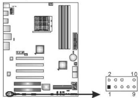
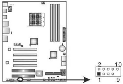
Diagram showing a computer room layout with labeled compartments and a directional arrow indicating flow or navigation.F USB1\~F USB3: Headers for USB 2.0 Ports at Front Panel
These headers allow user to connect additional USB cable on the PC front panel, and also can be connected with internal USB devices, like USB card reader.
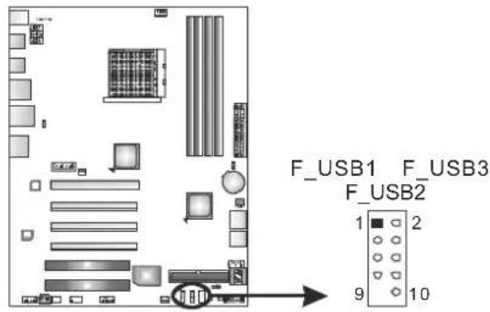
text_image
F_USB1 F_USB3 F_USB2 1 2 9 10| Pin | Assignment |
| 1 | +5V (fused) |
| 2 | +5V (fused) |
| 3 | USB- |
| 4 | USB- |
| 5 | USB+ |
| 6 | USB+ |
| 7 | Ground |
| 8 | Ground |
| 9 | Key |
| 10 | NC |
JUSBV1/JUSBV2: Power Source Headers for USB Ports
Pin 1-2 Close:
JUSBV1: +5V for USB ports at USB1/USB_1394_ESATA1/RJ45USB1.
JUSBV2: +5V for USB ports at F_USB1/F_USB2/F_USB3.
Pin 2-3 Close:
JUSBV1: +5V STB for USB ports at USB1/USB_1394_ESATA1/RJ45USB1.
JUSBV2: +5V STB for USB ports at F_USB1/F_USB2/F_USB3.
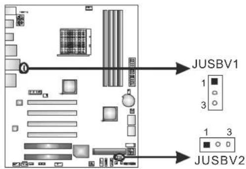
text_image
JUSBV1 1 3 1 3 JUSBV2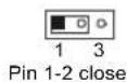
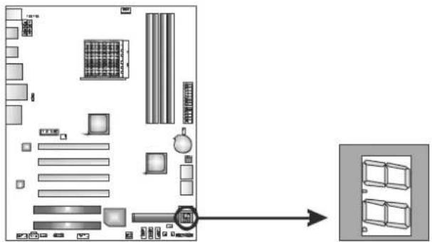
On-Board LED Indicators
There are 6 LED indicators showing system status.
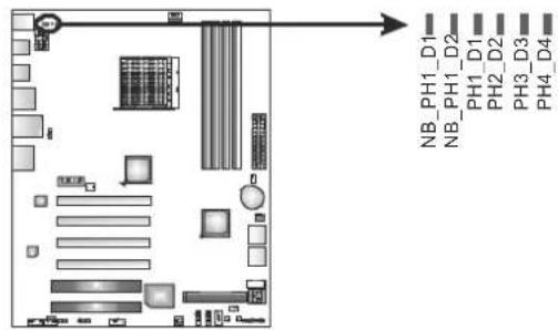
text_image
NB_PH1_D1 NB_PH1_D2 PH1_D1 PH2_D2 PH3_D3 PH4_D4NB_PH1_D1/NB_PH1_D2: NB Power Status Indicators
PH1_D1/PH2_D2/PH3_D3/PH4_D4: CPU Power Status Indicators Please refer to the tables below for specific messages:
| LED Phase Indicator | ||
| ON | Phase | Active |
| OFF | Phase | Disable |
On-Board Buttons
There are 2 on-board buttons.
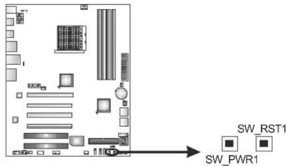
text_image
SW_RST1 SW_PWR1SW_RST1: Reset button.
SW_PWR1: Power Switch button.
CHAPTER 4: CROSSFIREX FUNCTION
4.1 CROSSFIREX INTRODUCTION
CrossFireX (also known as ATI CrossFire) is a brand name for ATI Technologies' multi-GPU solution. The technology enables two or more discrete graphics processors to work together in a single computer to improve graphics performance.
4.2 CROSSFIREX CONFIGURATION
Insert the Hybrid CrossFireX-Ready graphics card into PEX16_1, PEX16_3, or PEX16_4. Please refer to the following table to activate CFX function.
| CFX Status | PEX16_1 | PEX16_2 | PEX16_3 | PEX16_4 |
| PEX16_1 | — | X | O | O |
| PEX16_2 | X | — | X | X |
| PEX16_3 | O | X | — | O |
| PEX16_4 O | X | O | — |
(O: slot installed; X: slot not installed)
CHAPTER 5: RAID FUNCTIONS
Supports Windows Vista and Windows 7.
5.2 RAID ARRAYS
RAID supports the following types of RAID arrays:
RAID 0: RAID 0 defines a disk striping scheme that improves disk read and write times for many applications.
RAID 1: RAID 1 defines techniques for mirroring data.
RAID 10: RAID 10 combines the techniques used in RAID 0 and RAID 1.
RAID 5: RAID 5 provides fault tolerance and better utilization of disk capacity.
5.3 How RAID WORKS
RAID 0:
The controller “stripes” data across multiple drives in a RAID 0 array system. It breaks up a large file into smaller blocks and performs disk reads and writes across multip le drives in parallel. The size of each block is determined by the stripe size parameter, which you set during the creation of the RAID set based on the system environment. This technique reduces overall disk access time and offers high bandwidth.
Features and Benefits
- Drives: Minimum 2, and maximum is up to 6 or 8. Depending on the platform.
- Uses: Intended for non-critical data requiring high data throughput, or any environment that does not require fault tolerance.
- Benefits: provides increased data throughput, especially for large files. No capacity loss penalty for parity.
- Drawbacks: Does not deliver any fault tolerance. If any drive in the array fails, all data is lost.
- Fault Tolerance: No.
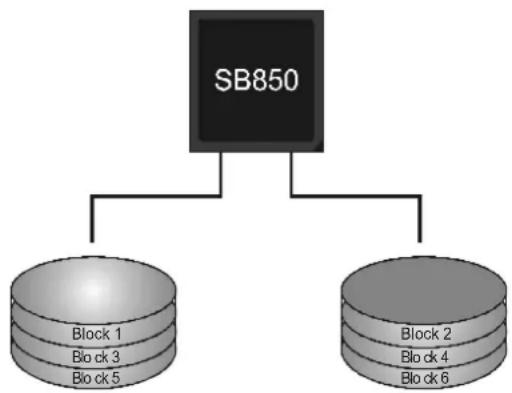
flowchart
graph TD
    A["SB850"] --> B["Block 1\nBlock 3\nBlock 5"]
    A --> C["Block 2\nBlock 4\nBlock 6"]
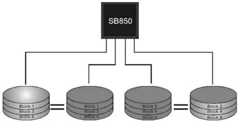
RAID 1:
Every read and write is actually carried out in parallel across 2 disk drives in a RAID 1 array system. The mirrored (backup) copy of the data can reside on the same disk or on a second redundant drive in the array. RAID 1 provides a hot-standby copy of data if the active volume or drive is corrupted or becomes unavailable because of a hardware failure.
RAID techniques can be applied for high-availability solutions, or as a form of automatic backup that eliminates tedious manual backups to more expensive and less reliable media.
Features and Benefits
- Drives: Minimum 2, and maximum is 2.
- Uses: RAID 1 is ideal for small databases or any other application that requires fault tolerance and minimal capacity.
- Benefits: Provides 100% data redundancy. Should one drive fail, the controller switches to the other drive.
- Drawbacks: Requires 2 drives for the storage space of one drive. Performance is impaired during drive rebuilds.
- Fault Tolerance: Yes.
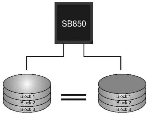
flowchart
graph TD
    A["SB850"] --> B["Block 1"]
    A --> C["Block 2"]
    A --> D["Block 3"]
    B --> E["=="]
    C --> E
    D --> E
RAID 10:
RAID 1 drives can be stripped using RAID 0 techniques. Resulting in a RAID 10 solution for improved resiliency, performance and rebuild performance.
Features and Benefits
- Drives: Minimum 4, and maximum is 6 or 8, depending on the platform.
- Benefits: Optimizes for both fault tolerance and performance, allowing for automatic redundancy. May be simultaneously used with other RAID levels in an array, and allows for spare disks.
- Drawbacks: Requires twice the available disk space for data redundancy, the same as RAID level 1.
- Fault Tolerance: Yes.
flowchart
graph TD
    A["SB850"] --> B["Block 1\nBlock 3\nBlock 5"]
    A --> C["Block 1\nBlock 3\nBlock 5"]
    A --> D["Block 2\nBlock 4\nBlock 6"]
    A --> E["Block 2\nBlock 4\nBlock 6"]
    B <--> C
    C <--> D
    D <--> E
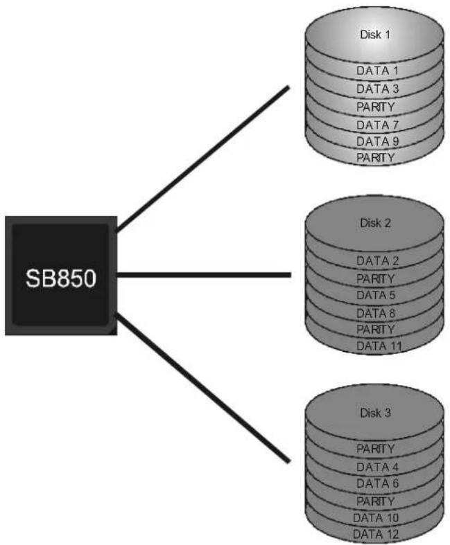
RAID 5:
RAID 5 stripes both data and parity information across three or more drives. It writes data and parity blocks across all the drives in the array. Fault tolerance is maintained by ensuring that the parity information for any given block of data is placed on a different drive from those used to store the data itself.
Features and Benefits
- Drives: Mini mum 3.
- Uses: RAID 5 is recommended for transaction processing and general purpose service.
- Benefits: An ideal combination of good performance, good fault tolerance, and high capacity and storage efficiency.
- Drawbacks: Individual block data transfer rate same as a single disk. Write performance can be CPU intensive.
- Fault Tolerance: Yes.
flowchart
graph TD
    A["SB850"] --> B["Disk 1"]
    A --> C["Disk 2"]
    A --> D["Disk 3"]
    B --> E["DATA 1"]
    B --> F["DATA 3"]
    B --> G["PARITY"]
    B --> H["DATA 7"]
    B --> I["DATA 9"]
    B --> J["PARITY"]
    C --> K["DATA 2"]
    C --> L["PARITY"]
    C --> M["DATA 5"]
    C --> N["DATA 8"]
    C --> O["PARITY"]
    C --> P["DATA 11"]
    D --> Q["PARITY"]
    D --> R["DATA 4"]
    D --> S["DATA 6"]
    D --> T["PARITY"]
    D --> U["DATA 10"]
    D --> V["DATA 12"]
CHAPTER 6: T-SERIES BIOS & SOFTWARE
6.1 T-SERIES BIOS
T-Series BIOS Features
■ Overclocking Navigator Engine (O.N.E.)
■ Memory Integration Test (M.I.T., under Overclock Navigator Engine)
BIO-Flasher: Update BIOS file from USB Flash Drive or FDD
■ Self Recovery System (S.R.S)
Smart Fan Function
■ CMOS Reloading Program
!! WARNING !!
For better system performance, the BIOS firmware is being continuously updated. The BIOS information described below in this manual is for your reference only and the actual BIOS information and settings on board may be different from this manual. For further information of setting up the BIOS, please refer to the BIOS Manual in the Sctm CD.
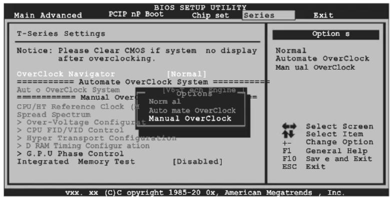
A. Overclocking Navigator Engine (O.N.E.)
ONE provides two powerful overclocking engines: MOS and AOS for both Elite and Casual overclockers.
| Main Advanced PCIPnP Boot Chipset Series Exit | |
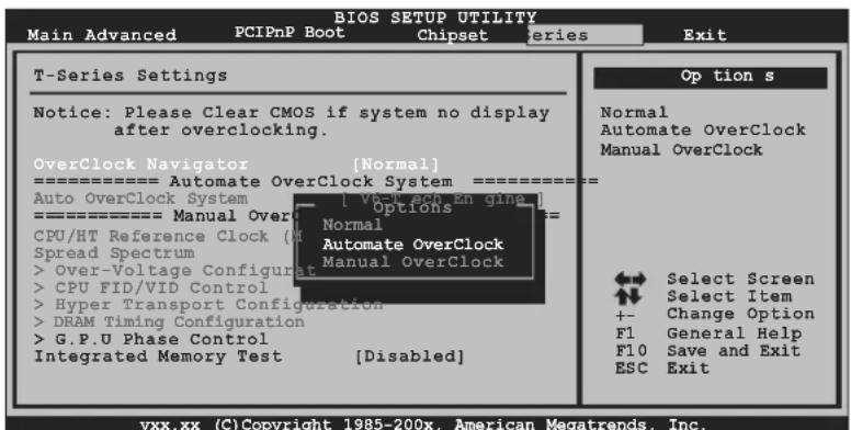
| T-Series Settings Notice: Please Clear CMOS if system no display after overclocking. OverClock Navigator [Normal] ==================== Automate OverClock System ==================== Auto OverClock System [V6-Tech Engine] ==================== Manual OverClock System ==================== CPU/HT Reference Clock (MHz) [200] Spread Spectrum [Disabled] >Over-Voltage Configuration >CPU FID/VID Control >Hyper Transport Configuration >DRAM Timing Configuration >G.P.U Phase Control Integrated Memory Test [Disabled] | Options Normal Automate OverClock Manual OverClock ↔ Select Screen ↔ Select Item +- Change Option F1 General Help F10 Save and Exit ESC Exit |
Manual Overclock System (M.O.S.)
MOS is designed for experienced overclock users.
It allows users to customize personal overclock settings.
text_image
BIOS SETUP UTILITY Main Advanced PCIP nP Boot Chip set Series Exit T-Series Settings Notice: Please Clear CMOS if system no display after overclocking. OverClock Navigator [Normal] ==================== Automate OverClock System ==================== Aut o OverClock System [VccTech Engine 1] ==================== Manual Over Clock Options CPU/HT Reference Clock (M Spread Spectrum > Over-Voltage Configurat > CPU FID/VID Control > Hyper Transport Configuration > D RAM Timing Configur ation > G.P.U Phase Control Integrated Memory Test [Disabled] Option s Normal Automate OverClock Manual OverClock Select Screen Select Item +- Change Option F1 General Help F10 Save e and Exit ESC Exit vxx. xx (C)C copyright 1985-20 0x, American Megatrends , Inc.↓
text_image
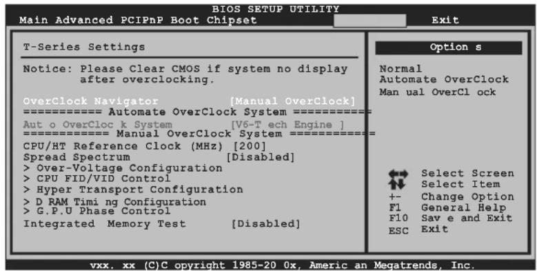
BIOS SETUP UTILITY Main Advanced PCIPnP Boot Chipset Exit T-Series Settings Notice: Please Clear CMOS if system no display after overclocking. OverClock Navigator [Manual OverClock] ================[Automate OverClock System ================== Aut o OverCloc k System [V6-T ech Engine ] ================[Manual OverClock System ================== CPU/HT Reference Clock (MHz) [200] Spread Spectrum [Disabled] > Over-Voltage Configuration > CPU FID/VID Control > Hyper Transport Configuration > D RAM Timi ng Configuration > G.P.U Phase Control Integrated Memory Test [Disabled] Option s Normal Automate OverClock Man ual OverCl ock Select Screen Select Item +- Change Option F1 General Help F10 Sav e and Exit ESC Exit vxx. xx (C)C opyright 1985-20 0x, Americ an Megatrends, Inc.CPU/HT Reference Clock (MHz)
This item allows BIOS to select CPU Over Clock.
Spread Spectrum
This item allows you to control Spread Spectrum function.
Over-Voltage Configuration
Enter this function for more advanced voltage settings.
CPU FID/VID Control
Enter this function for more advanced CPU settings.
Hyper Transport Configuration
Enter this function for more advanced Hyper Transport settings.
DRAM Timing Configuration
Enter this function for more advanced DRAM clock settings.
G.P.U Phase Control
Enter this function for more power saving settings.
NOTE
Overclock is an optional process, but not a “must-do” process; it is not recommended for inexperienced users. Therefore, we will not be responsible for any hardware damage which may be caused by overclocking. We also would not guarantee any overclocking performance.
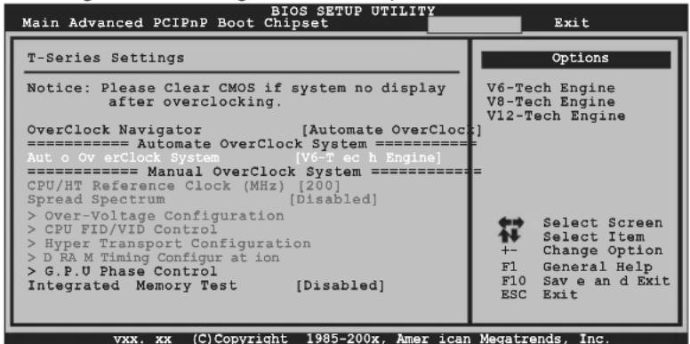
Automatic Overclock System (A.O.S.)
For beginners in overclock field, BET had developed an easy, fast, and powerful feature to increase the system performance, named A.O.S. Based on many tests and experiments, A.O.S. provides 3 ideal overclock configurations that are able to raise the system performance in a single step.
text_image
BIOS SETUP UTILITY Main Advanced PCIPnP Boot Chipset Series Exit T-Series Settings Notice: Please Clear CMOS if system no display after overclocking. OverClock Navigator [Normal] ==================== Automate OverClock System ==================== Auto OverClock System [V6-1ech En gine] ==================== Manual Over Clock Options CPU/HT Reference Clock (M Normal Spread Spectrum > Over-Voltage Configurat > CPU FID/VID Control > Hyper Transport Configuration > DRAM Timing Configuration > G.P.U Phase Control Integrated Memory Test [Disabled] Op tion s Normal Automate OverClock Manual OverClock ←→ Select Screen ↑→ Select Item +- Change Option F1 General Help F10 Save and Exit ESC Exit vxx.xx (C) Copyright 1985-200x, American Megatrends, Inc.V6 Tech Engine
This engine will make a good over-clock performance.
text_image
BIOS SETUP UTILITY Main Advanced PCIPnP Boot Chipset Exit T-Series Settings Notice: Please Clear CMOS if system no display after overclocking. OverClock Navigator [Automate OverClock] ==================== Automate OverClock System ==================== Aut o Ov erClock System [V6-T ec h Engine] ==================== Manual OverClock System ==================== CPU/HT Reference Clock (MHz) [200] Spread Spectrum [Disabled] > Over-Voltage Configuration > CPU FID/VID Control > Hyper Transport Configuration > D RA M Timing Configur at ion > G.P.U Phase Control Integrated Memory Test [Disabled] Options V6-Tech Engine V8-Tech Engine V12-Tech Engine Select Screen Select Item +- Change Option F1 General Help F10 Sav e an d Exit ESC Exit vxx. xx (C)Copyright 1985-200x, Amer ican Megatrends, Inc.V8 Tech Engine
This engine will make a better over-clock performance.
| T-Series Settings Notice: Please Clear CMOS if system no display after overclocking. OverClock Navigator [Automate OverClock] [Automate OverClock System] Aut o Ov erClock System [V8-T ec h Engine] [Manual OverClock System] CPU/HT Reference Clock (MHz) [200] Spread Spectrum [Disabled] > Over-Voltage Configuration > CPU FID/VID Control > Hyper Transport Configuration > D RA M Timing Configur at ion > G.P.U Phase Control Integrated Memory Test [Disabled] | Options V6-Tech Engine V8-Tech Engine V12-Tech Engine Select Screen Select Item + - Change Option F1 General Help F10 Sav e an d Exit ESC Exit |
V12 Tech Engine
This engine will make a best over-clock performance.
| T-Series Settings | Options | |
| Notice: Please Clear CMOS if system no display after overclocking. | V6-Tech Engine V8-Tech Engine V12-Tech Engine | |
| OverClock Navigator [Automate OverClock] | ||
| Auto OverClock System [V12-Tech Engine] | ||
| CPU/HT Reference Clock (MHz) [200] | ||
| Spread Spectrum [Disabled] | ||
| >Over-Voltage Configuration | Select Screen Select Item | |
| >CPU FID/VID Control | Change Option | |
| >Hyper Transport Configuration | General Help | |
| >D RA M Timing Configur at ion | Sav e and d Exit | |
| >G.P.U Phase Control | ESC Exit | |
| Integrated Memory Test [Disabled] | ||
Notices:
Not all types of AMD CPU perform above overclock setting ideally; the difference will be based on the selected CPU model.
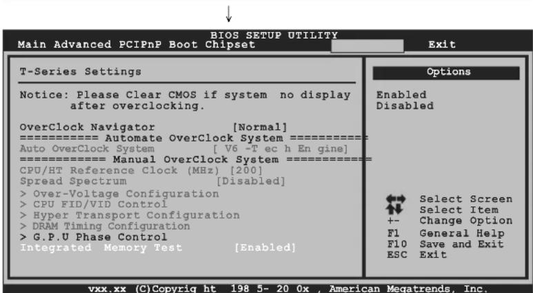
B. Memory Integration Test (M.I.T.)
This function is under "Overclocking Navigator Engine" item.
MIT allows users to test memory compatibilities, and no extra devices or software are needed.
Step 1
The default setting under this item is "Disabled"; the condition parameter should be changed to "Enable" to proceed this test.
| T-Series Settings | Options | |
| Notice: Please Clear CMOS if system no display after overclocking. | Enabled Disabled | |
| OverClock Navigator [Normal]================equal to Automate OverClock System ================== | ||
| Auto OverClock System [V6 -T ec h En gine]================equal to Manual OverClock System ================== | ||
| CPU/HT Reference Clock (MHz) [200] | ||
| Spread Spectrum [Disabled] | ||
| >Over-Voltage Configuration | Select Screen Select Item | |
| >CPU FID/VID Control | ||
| >Hyper Transport Configuration | Change Option | |
| >DRAM Timing Configuration | General Help | |
| >G.P.U Phase Control | Save and Exit | |
| Integrated Memory Test [Disabled] | ESC Exit | |
text_image
BIOS SETUP UTILITY Main Advanced PCIPnP Boot Chipset Exit T-Series Settings Notice: Please Clear CMOS if system no display after overclocking. OverClock Navigator [Normal] ==================== Automate OverClock System ==================== Auto OverClock System [ V6 -T ec h En gine ] ==================== Manual OverClock System ==================== CPU/HT Reference Clock (MHz) [200] Spread Spectrum [Disabled] > Over-Voltage Configuration > CPU FID/VID Control > Hyper Transport Configuration > DRAM Timing Configuration > G.P.U Phase Control Integrated Memory Test [Enabled] Options Enabled Disabled Select Screen Select Item +- Change Option F1 General Help F10 Save and Exit ESC Exit vxx.xx (C)Copyright ht 198 5- 20 0x , American Megatrends, Inc.Step 2
Save and Exit from CMOS setup and reboot the system to activate this test.
Run this test for 5 minutes (minimum) to ensure the memory stability.
Step 3
When the process is done, change the setting back from "Enable" to "Disable" to complete the test.
C. BIO-Flasher
BIO-Flasher is a BIOS flashing utility providing you an easy and simple way to update your BIOS via USB pen drive or floppy disk.
The BIO-Flasher is built in the BIOS chip. To enter the utility, press
Updating BIOS with BIO-Flasher
- Go to the website to download the latest BIOS file for the motherboard.
- Then, save the BIOS file into a USB pen drive or a floppy disk.
- Insert the USB pen drive or the floppy disk that contains the BIOS file to the USB port or the floppy disk drive.
- Power on or reset the computer and then press
during the POST process. A select dialog as the picture on the right appears. Select the device contains the BIOS file and press to enter the utility.
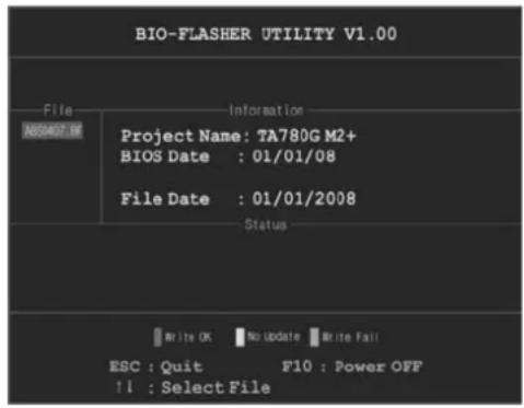
text_image
BIO-FLASHER UTILITY V1.00 File Information Project Name: TA780G M2+ BIOS Date : 01/01/08 File Date : 01/01/2008 Status Write OK No Update Write Fail ESC : Quit F10 : Power OFF ↑↓ : Select File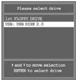
text_image
Please select drive 1st FLOPPY DRIVE USB: USB DISK 2.0 ↑ and ↓ to move selection ENTER to select drive-
The utility will show the BIOS files and their respective information. Select the proper BIOS file and press
then to perform the BIOS update process. -
After the update process, the utility will ask you to reboot the system. Press
to proceed. BIOS update completes.

- This utility only allows storage device with FAT32/16 format and single partition.
- Shutting down or resetting the system while updating the BIOS will lead to system boot failure.
D. Self Recovery System (S.R.S.)
This function can't be seen under BIOS setup; and is always on whenever the system starts up.
However, it can prevent system hang-up due to inappropriate overclock actions.
When the system hangs up, S.R.S. will automatically log in the default BIOS setting, and all overclock settings will be re-configured.
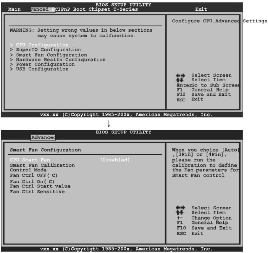
E. Smart Fan Function
Smart Fan Function is under "Smart Fan Configuration" in "Advanced Menu". This is a brilliant feature to control CPU/System Temperature vs. Fan speed. When enabling Smart Fan function, Fan speed is controlled automatically by CPU/System temperature.
This function will protect CPU/System from overheat problem and maintain the system temperature at a safe level.
text_image
BIOS SETUP UTILITY Main Vanced PCIPnP Boot Chipset T-Series Exit WARNING: Setting wrong values in below sections may cause system to malfunction. >CPU Configuration >SuperIO Configuration >Smart Fan Configuration >Hardware Health Configuration >Power Configuration >USB Configuration Configure CPU.Advanced Settings Select Screen Select Item EnterGo to Sub Screen F1 General Help F10 Save and Exit ESC Exit vxx.xx (C)Copyright 1985-200x, American Megatrends, Inc. ↓ BIOS SETUP UTILITY Advanced Smart Fan Configuration CPU Smart Fan [Disabled] Smart Fan Calibration Control Mode Fan Ctrl OFF( C) Fan Ctrl On( C) Fan Ctrl Start value Fan Ctrl Sensitive When you choice [Auto], ,[3Pin] or [4Pin], please run the calibration to define the Fan parameters for Smart Fan control Select Screen Select Item +- Change Option F1 General Help F10 Save and Exit ESC Exit vxx.xx (C)Copyright 1985-200x, American Megatrends, Inc.Smart Fan Calibration
Choose this item and then the BIOS will automatically test and detect the CPU/System fan functions and show CPU/System fan speed.
Control Mode
This item provides several operation modes of the fan.
Fan Ctrl OFF(°C)
If the CPU/System temperature is lower than the set value, the CPU/System fan will turn off. The range is from 0\~127, with an interval of 1.
Fan Ctrl On(°C)
The CPU/System fan starts to work when CPU/System temperature arrives to this set value. The range is from 0\~127, with an interval of 1.
Fan Ctrl Start Value
When CPU/System temperature arrives to the set value, the CPU/System fan will work under Smart Fan Function mode. The range is from 0\~127, with an interval of 1.
Fan Ctrl Sensitive
Increasing the value of slope PWM will raise the speed of CPU/System fan. The range is from 1\~127, with an interval of 1.
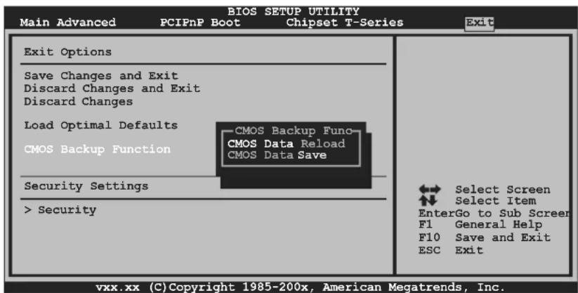
F. CMOS Reloading Program
It allows users to save different CMOS settings into BIOS-ROM.
Users are able to reload any saved CMOS setting for customizing system configurations. Moreover, users are able to save an ideal overclock setting during overclock operation.
There are 10 sets of record addresses in total, and users are able to name the CMOS data according to personal preference.
text_image
Main Advanced PCIPnP Boot Chipset T-Series Exit BIOS SETUP UTILITY Exit Options Save Changes and Exit Discard Changes and Exit Discard Changes Load Optimal Defaults CMOS Backup Func CMOS Backup Function CMOS Data Reload CMOS Data Save Security Settings > Security Select Screen Select Item EnterGo to Sub Screen F1 General Help F10 Save and Exit ESC Exit vxx.xx (C)Copyright 1985-200x, American Megatrends, Inc.6.2 T-SERIES SOFTWARE
Installing T-Series Software
- Insert the Setup CD to the optical drive. The drivers installation program would appear if the Auto-run function has been enabled.
- Select Software Installation, and then click on the respective software title.
- Follow the on-screen instructions to complete the installation.
Launching T-Series Software
After the installation process is completed, you will see the software icon showing on the desktop. Double-click the icon to launch it.
TOverclocker
TOverclocker presents a simple Windows-based system performance enhancement and manageability utility. It features several powerful and easy to use tools such as Overclocking for enhancing system performance, also for special enhancement on CPU and Memory. Smart-Fan management and PC health are for monitoring system status. This utility also allows you to make overclocking profiles saving unlimitedly, and pre-set OC modes are for easy OC. (The illustration below is for reference only)

text_image
CPU MEMORY OC TWEAKER H/W MONITOR OVERCLOCKER Clocks Clock Speed: 916.1 MHz Multiplier: x 4 HT Link: 2290.1 MHz Bus Speed: 229.0 MHz MotherBoard Model: TA890GKE BIOS: AMI BIOS BIOS Data: 01/26/10 BIOS File Name: B9GAP126 BS Processor Name: AMD Phenom II 905e Specification: AMD Phenom(1m) II MI 905e Processor Instructions: MMX(+),3DNow(+),SSE,SSE2, SSE3,SSE4A,X66-64 Code Name: Denseb L1-D Cache: 4 x 64 KBytes Technology: 45 nm L1-I Cache: 4 x 64 KBytes Voltage: 0.34BV L2 Cache: 4 x 512 KBytes Package: Socket AM3 L3 Cache: 5144 KBytes Family: F Ext. Family: 10 Model: 4 Ext Model: 4 Stopping: 2 Revision: C2Motherboard Manual

The CPU tab provides information on the CPU and motherboard.

The Memory tab provides information on the memory module(s).
You can select memory module on a specific slot to see its information.

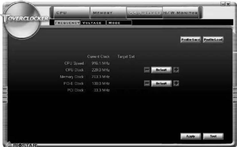
The OC Tweaker tab allows you to change system clock settings and voltages settings. It also provides six pre-set modes for you:
text_image
OVERCLOCKER CPU MEMORY OGWEAKER H/W MONITOR FREQUENCY VOLTAGE MODE Profile Save Profile Load Current Clock Target Set CPU Speed 316.1 MHz CPU Clock 229.0 MHz Default + Memory Clock 7E3.3 MHz PCI-E Clock 100.0 MHz Default + PCI Clock 33.3 MHz Apply TestSix Pre-set Modes: V3, V6, V9, V12, V15, AUTO for different overclocking experience.
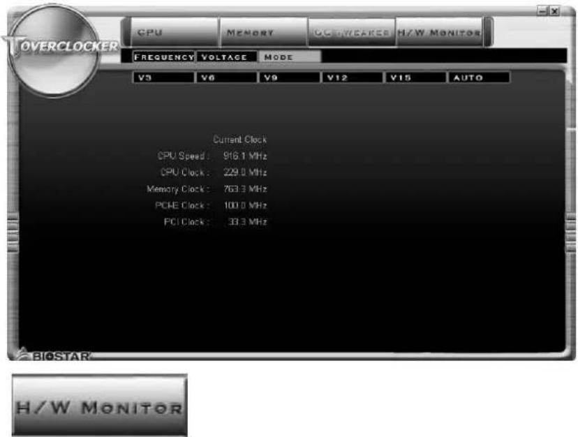
text_image
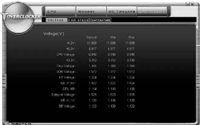
OVERCLOCKER CPU MEMORY GO/TWEACES H/W MONITOR FREQUENCY VOLTAGE MODE V3 V6 V9 V12 V15 AUTO Current Clock CPU Speed: 916.1 MHz CPU Clock: 229.0 MHz Memory Clock: 763.3 MHz PCHE Clock: 100.0 MHz PCI Clock: 33.3 MHz H/W MONITORThe HW Monitor tab allows you to monitor hardware voltage, fan speed, and temperature. Besides, you also can set related values for CPU Smart Fan.
text_image
OVERCLOCKER CPU MEMORY DC-TWEAKER MAX/MONITOR VOLTAGE FAN SPEED TOMPERATURE Voltage(V) Current Max Max +12V: 11.869 11.869 11.869 +5.0V: 4.977 4.977 4.977 CPU Voltage: 0.940 0.940 0.940 +3.3V: 3.312 3.312 3.336 Chip Voltage: 1.368 1.368 1.368 DDR Voltage: 1.572 1.572 1.572 HT Voltage: 1.224 1.224 1.224 MB +1.8V: 1.822 1.822 1.824 CPU NB: 1.114 1.110 1.118 Sideport Voltage: 1.526 1.523 1.525 NB +1.1V: 1.120 1.116 1.120 SB Voltage: 1.122 1.120 1.122
Pressing TOVERCLOCKER logo will display information about manufacturer and software version. You can update cummet version by clicking the button "Live Update."
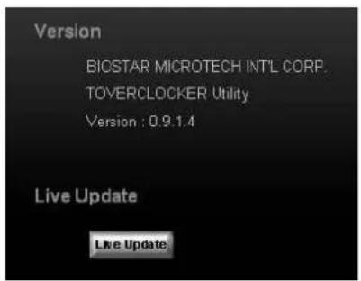
text_image
Version BICSTAR MICROTECH INT'L CORP. TOVERCLOCKER Utility Version : 0.9.1.4 Live Update Live UpdateGreen Power II Utility
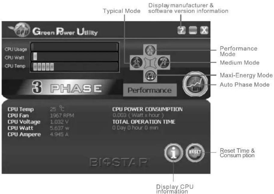
BIOSTAR G.P.U II (Green Power Utility) is a new function. The utility enhances energy efficiency by disabling extra phases while CPU is on light loading; it features 4+1 power phases, current power saving, and toal power saving. This tool integrates a friendly GUI to monitor your CPU Usage, CPU Watt, and CPU Temperature. Moreover, it optimizes power saving and best power efficiency on your system. (The illustration below is for reference only)
text_image
Typical Mode Display manufacturer & software version information Green Power Utility CPU Usage CPU Watt CPU Temp 3 PHASE Performance Mode Medium Mode Maxi-Energy Mode Auto Phase Mode CPU Temp 25 °C CPU Fan 1967 RPM CPU Voltage 1.032 V CPU Watt 5.637 W CPU Ampere 4.945 A CPU POWER CONSUMPTION 0.003 (Watt x hour) TOTAL OPERATION TIME 0 Day 0 hour 0 min Reset Time & Consumption BI4STAR Display CPU informationG.P.U Mode Setting
This utility provides five modes, upon your requirements, to improve system performance or to save power consumption.
Note: Even if the modes saving more power consumption are chosen, the system still can keep excellent performance.
■ Auto Phase Mode
System switches the mode automatically according to current system loading condition.
■ Performance Mode
This is the mode saving power consumption most. Least energy will be used in the system.
■ Typical Mode
Compared with that in Performance Mode, energy consumption in this mode is a little bit more.
■ Medium Mode
This is the standard system power saving mode.
■ Maxi-Energy Mode
This is the best system performance mode.
eHot-Line (Optional)
eHot-Line is a convenient utility that helps you to contact with our Tech-Support system. This utility will collect the system information which is useful for analyzing the problem you may have encountered, and then send these information to our tech-support department to help you fix the problem.

Before you use this utility, please set Outlook Express as your default e-mail client application program.
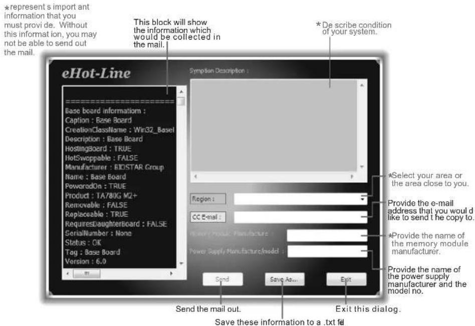
text_image
eHot-Line Base board information : Caption : Base Board CreationClassName : Win32_Basel Description : Base Board HostingBoard : TRUE HotSwappable : FALSE Manufacturer : BIOSTAR Group Name : Base Board PowerodOn : TRUE Product : TA780G M2+ Removable : FALSE Replaceable : TRUE RequiresDaughterBoard : FALSE SerialNumber : None Status : OK Tag : Base Board Version : 6.0 Symptom Description : Region : CC E-mail : Send Save As... Exit *Represent s import an information that you must provi de. Without this inforat ion, you may not be able to send out the mail. This block will show the information which would be collected in the mail. *De scribe condition of your system. *Select your area or the area close to you. Provide the e-mail address that you would like to send t he copy to. *Provide the name of the memory module manufacturer. Provide the name of the power supply manufacturer and the model no. Send the mail out. Save these information to a .txt fil Exit this dialog.After filling up this information, click "Send" to send the mail out. A warning dialog would appear asking for your confirmation; click "Send" to confirm or "Do Not Send" to cancel.
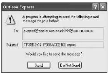
text_image
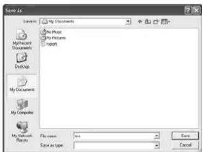
Outlook Express A program is attempting to send the following e-mail message on your behalf: To: support@biostar.usa.com/XX-XX-XX-XX-XX Subject: TP35D2A7 (P35BAC05 BSI) report Would you like to send the message? Send Do Not SendIf you want to save this information to a .txt file, click "Save As..." and then you will see a saving dialog appears asking you to enter file name.
Enter the file name and then click "Save". Your system information will be saved to a .txt file.
text_image
base sound information Caption : Base Sound Creation: TamaName, wnl2_Ravebound Description : Base Award Moodboard : 3rd Manufacturer : Blotar/Grub Name : Base Board Copyright : 3rd Product : 191502-2 Cartelaware : 1 Tag : Base Sound Version : 1 RSDS Information Caption : Phoenix - air@100.com Subramlingue : 1915188883- System: (New) - air@100.com Initiate: languages : 1 Manufacturer : Phoenix Technologies, LTD. Name : Phoenix - air@100.com Ref: 1915188883_0000000000000000000000000000000000000000000000000000000000000000000000000000000000000000000000000000 File Name : 1 SMDS Information : 6.6.6.6.6 Software: version 1 : 1 system: version 1 : 1 Software: version 1 : 1 Status : OK Computer: System: 1 Version : InteA - 42326331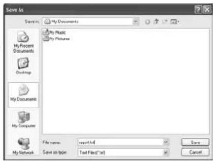
text_image
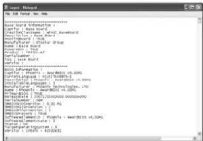
Save As My Documents My Music My Pictures My Recent Documents Desktop My Documents My Computer My Network File name: report.txt Save as type: Text Files(*.txt) Save CancelOpen the saved .txt file, you will see your system information including motherboard/BIOS/CPU/video/device/OS information. This information is also concluded in the sent mail.

We will not share customer's data with any other third parties, so please feel free to provide your system information while using eHot-Line service.

If you are not using Outlook Express as your default e-mail client application, you may need to save the system information to a .txt file and send the file to our tech support with other e-mail application. Go to the following web http://www.biostar.com.tw/app/en-us/about/contact.php for getting our contact information.
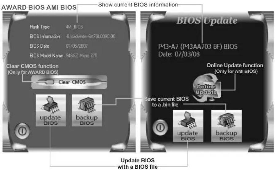
BIOS Update
BIOS Update is a convenient utility which allows you to update your motherboard BIOS under Windows system.
text_image
AWARD BIOS AMI BIOS Show current BIOS information Flash Type 4M_BIOS BIOS Information Broadwate 6A79L003C-00 BIOS Date 01/05/2007 BIOS Model Name 946GZ Micro 775 Clear CMOS function (Only for AWARD BIOS) Clear CMOS P43-A7 (P43AA703 BF) BIOS Date: 07/03/08 Online Update function (Only for AMI BIOS) online Update Save current BIOS to a .bin file Update BIOS with a BIOS fileOnce click on this button, the saving dialog will show. Choose the position to save file and enter file name. (We recommend that the file name should be English/number and no longer than 7 characters.) Then click Save.
text_image
Save As Documents My Documents My Music My Pictures Import My Historic Documents Desktop My Documents My Computer My Network Places File name: unt Save as type: Save As CancelBefore doing this, please download the proper BIOS file from the website.
For AWARD BIOS, update BIOS procedure should be run with Clear CMOS function, so please check on Clear CMOS first.
text_image
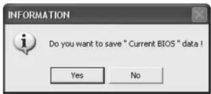
INFORMATION Do you want to save " Current BIOS " data ! Yes NoThen click Update BIOS button, a dialog will show for asking you backup current BIOS. Click Yes for BIOS backup and refer to the Backup BIOS procedure; or click No to skip this procedure.
After the BIOS Backup procedure, the open dialog will show for requesting the BIOS file which is going to be updated. Please choose the proper BIOS file for updating, then click on Open.
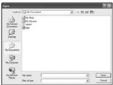
text_image
Open Look in: My Documents My Music My Pictures Report Text My Documents My Computer My Network Files File name: File of type: Open Cancel
text_image
BIOS 35% Programming Main BlockThe utility will update BIOS with the proper BIOS file, and this process may take minutes. Please do not open any other applications during this process.
After the BIOS Update process, click on OK to restart the system.
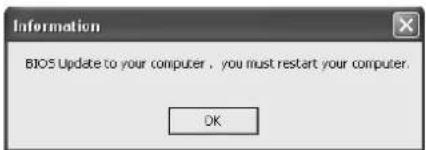
text_image
Information BIOS Update to your computer, you must restart your computer. OKWhile the system boots up and the full screen logo shows, press
In the BIOS setup, use the Load Optimized Defaults function and then Save and Exit Setup to exit BIOS setup. BIOS Update is completed.
Automatically download and update the latest BIOS via internet; make sure that the computer is connected to the internet before using this function.
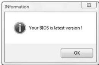
After clicking on the Onlinr Update button, the utility will search for the latest BIOS from internet. If there is a new BIOS version, the utility will ask you to download it. Click Yes to proceed.
text_image
INformation Your BIOS is latest version ! OKDownload completes; the utility will ask you to program (update) the BIOS. Click Yes to proceed.
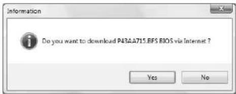
text_image
Information Do you want to download P43AA715.EFS BIOS via Internet ? Yes NoIf there is no other newer BIOS version, the utility will also tell you that your BIOS has been the latest version.
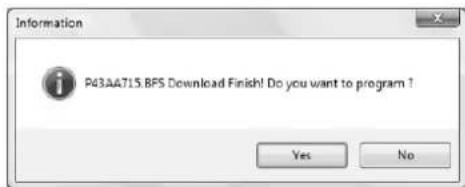
text_image
Information P43AA715.BFS Download Finish! Do you want to program ? Yes NoThe programing procedure may take minutes, please do not make any operation during the programing process.
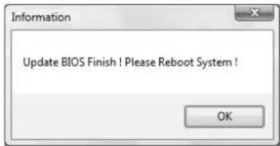
text_image
Information Update BIOS Finish ! Please Reboot System ! OKAfter the updating process, the utility will ask you to reboot the system. Click OK to reboot.
While the system boots up and the full screen logo shows, press Del
In the BIOS setup, use the Load Optimized Defaults function and then Save and Exit Setup to exit BIOS setup. Online Update is completed.

All the information and content above about the T-Series software are subject to be changed without notice. For better performance, the software is being continuously updated. The information and pictures described above are for your reference only. The actual information and settings on board may be slightly different from this manual.
CHAPTER 7: USEFUL HELP
7.1 DRIVER INSTALLATION NOTE
After you installed your operating system, please insert the Fully Setup Driver CD into your optical drive and install the driver for better system performance.
You will see the following window after you insert the CD
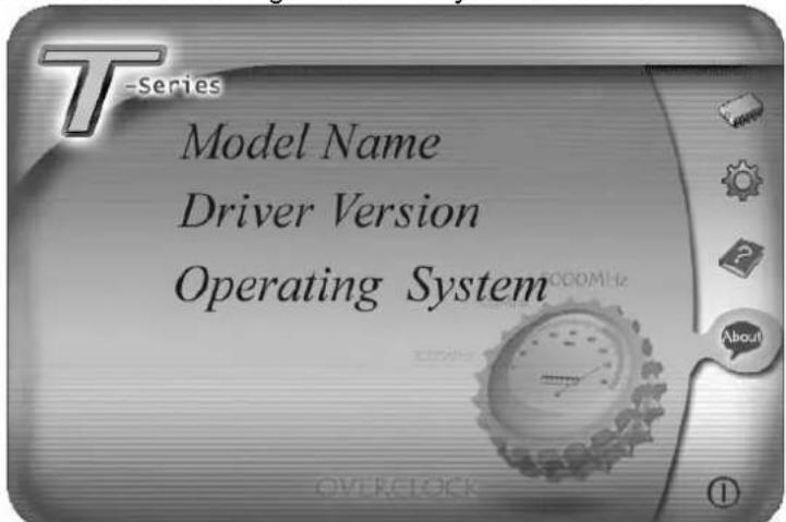
text_image
T-Series Model Name Driver Version Operating SystemThe setup guide will auto detect your motherboard and operating system.
Note:
If this window didn't show up after you insert the Driver CD, please use file browser to locate and execute the file SETUP.EXE under your optical drive.
A. Driver Installation
To install the driver, please click on the Driver icon. The setup guide will list the compatible driver for your motherboard and operating system. Click on each device driver to launch the installation program.
B. Software Installation
To install the software, please click on the Software icon. The setup guide will list the software available for your system, click on each software title to launch the installation program.
C. Manual
Aside from the paperback manual, we also provide manual in the Driver CD. Click on the Manual icon to browse for available manual.
Note:
You will need Acrobat Reader to open the manual file. Please download the latest version of Acrobat Reader software from http://www.adobe.com/products/acrobat/readstep2.html
7.2 EXTRA INFORMATION
CPU Overheated
If the system shutdown automatically after power on system for seconds, that means the CPU protection function has been activated.
When the CPU is over heated, the motherboard will shutdown automatically to avoid a damage of the CPU, and the system may not power on again.
In this case, please double check:
- The CPU cooler surface is placed evenly with the CPU surface.
- CPU fan is rotated normally.
- CPU fan speed is fulfilling with the CPU speed.
After confirmed, please follow steps below to relief the CPU protection function.
- Remove the power cord from power supply for seconds.
- Wait for seconds.
- Plug in the power cord and boot up the system.
Or you can:
- Clear the CMOS data.
(See "Close CMOS Header: JCMOS1" section) - Wait for seconds.
- Power on the system again.
7.3 AMI BIOS BEEP CODE
Boot Block Beep Codes
| Number of Beeps | Description |
| 1 No media present. (Insert diskette in floppy drive A:) | |
| 2 | “AMIBOOT.ROM” file not found in root directory of diskette in A: |
| 3 Insert next diskette if multiple diskettes are used for recovery | |
| 4 Flash Programming successful | |
| 5 File read error | |
| 7 No Flash EPROM detected | |
| 10 Flash Erase error | |
| 11 Flash Program error | |
| 12 “AMIBOOT.ROM” file size error | |
| 13 | BIOS ROM image mismatch (file layout does not match image present in flash device) |
POST BIOS Beep Codes
| Number of Beeps | Description |
| 1 Memory | refresh timer error |
| 3 Base memory | read/write test error |
| 6 Keyboard controller BAT command failed | |
| 7 General exception error (processor exception interrupt error) | |
| 8 Display memory error (system video adapter) | |
Troubleshooting POST BIOS Beep Codes
| Number of Beeps | Troubleshooting Action |
| 1, 3 Reseat | the memory, or replace with known good modules. |
| 6, 7 | Fatal error indicating a serious problem with the system. Consult your system manufacturer. Before declaring the motherboard beyond all hope, eliminate the possibility of interference by a malfunctioning add-in card. Remove all expansion cards except the video adapter.If beep codes are generated when all other expansion cards are absent, consult your system manufacturer's technical support.If beep codes are not generated when all other expansion cards are absent, one of the add-in cards is causing the malfunction. Insert the cards back into the system one at a time until the problem happens again. This will reveal the malfunctioning card. |
| 8 | If the system video adapter is an add-in card, replace or reseat the video adapter. If the video adapter is an integrated part of the system board, the board may be faulty. |
7.4 AMI BIOS POST CODE
| Checkpoint | Description |
| 03 | Disable NMI, Parity, video for EGA, and DMA controllers. Initialize BIOS, POST, Runtime data area. Also initiali ze B IOS mod ules on POST entry and GPNV area. Initialized CMOS as mentioned in the Kernel Variable "wCMOSFlags." |
| 04 | Check CMOS diagnostic byte to determine if battery power is OK and CMOS checksum is OK. Verify CMOS checksum manually by reading storage area. If the CMOS checksum is bad, update CMOS with power-on default values and clear passwords. Initialize status register A. Initializes data variables that are based on CMOS setup questions. Initializes both the 8259 compatible PICs in the system |
| 05 | Initializes the interrupt controlling hardware (generally PIC) and interrupt vector table. |
| 06 | Do R/W test to C H-2 count reg. Initiali ze CH-0 as system timer. Install the POSTINT1C h handler. E nable IRQ-0 in P IC for system timer interrupt. Traps INT1Ch vector to "POSTINT1ChHandlerBlock." |
| 07 Fixes | CPU POST interface calling pointer. |
| 08 | Initiali zes the CPU. The BAT test is being done on KBC. Program the keyboard controller command byte is being done after Auto detection of KB/MS using AMI KB-5. |
| C0 Early CPU Init Start -- Disable Cache - Init Local APIC. | |
| C1 Set up boot strap processor Information. | |
| C2 Set up boot strap processor for POST. | |
| C5 Enumerate and set up application processors. | |
| C6 Re-enable cache for boot strap processor. | |
| C7 Early CPU Init Exit. | |
| 0A Initializes the 8042 compatible Key Board Controller. | |
| 0B Detects the presence of PS/2 mouse. | |
| 0C Detects the presence of Keyboard in KBC port. | |
| 0E | Testing and initialization of different Input Devices. Also, update the Kernel Variables. Traps the INT09h vector, so that the POST INT09h handler ge ts control for IRQ1. Uncompress all available language, BIOS logo, and Silent logo modules. |
| 13 Early POST initialization of chipset registers. | |
| 20 Relocate System Management Interrupt vector for all CPU in the system. | |
| 24 | Uncompress a nd i initialize a ny platform specific B IOS mod ules. GPNV is initialized at this checkpoint. |
| 2A | Initializes different devices through DIM. See DIM Code Checkpoints section of document for more information. |
| 2C | Initializes different devices. Detects and initializes the video adapter installed in the system that have optional ROMs. |
| 2E Initializes all the output devices. | |
| 31 | Allocate memory for ADM module and uncompress it. Give control to ADM module for initialization. Initialize language and font modules for ADM. Activate ADM module. |
| 33 | Initializes the silent boot module. Set the window for displaying text information. |
| 37 | Displaying sign-on message, CPU information, setup key message, and any OEM specific information. |
| 38 | Initializes different devices through DIM. See DIM Code Checkpoints section of document for more information. USB controllers are initialized at this point. |
| 39 | Initializes DMAC-1 & DMAC-2. |
| 3A | Initialize RTC date/time. |
| 3B | Test for total memory installed in the system. Also, Check for DEL or ESC keys to limit memory test. Display total memory in the system. |
| 3C Mid | POST initialization of chipset registers. |
| 40 | Detect different devices (Parallel ports, serial ports, and coprocessor in CPU, etc.) successfully installed in the system and update the BDA, EBDA...etc. |
| 52 | Updates CMOS memory size from memory found in memory test. Allocates memory for Extended BIOS Data Area from base memory. Programming the memory hole or any kind of implementation that needs an adjustment in system RAM size if needed. |
| 60 | Initializes NUM-LOCK status and programs the KBD typematic rate. |
| 75 | Initialize Int-13 and prepare for IPL detection. |
| 78 | Initializes IPL devices controlled by BIOS and option ROMs. |
| 7C | Genera te a nd write contents of ESCD in NVRam. |
| 84 | Log errors encountered during POST. |
| 85 | Display errors to the user and gets the user response for error. |
| 87 | Execute BIOS setup if needed / requested. Check boot password if installed. |
| 8C | Late POST initialization of chipset registers. |
| 8D | Build ACPI tables (if ACPI is supported). |
| 8E | Program the peripheral parameters. Enable/Disable NMI as selected. |
| 90 | Initialization of system management interrupt by invoking all handlers. Please note this checkpoint comes right after checkpoint 20h. |
| A1 | Clean-up work needed before booting to OS. |
| A2 | Takes care of runtime image preparation for different BIOS modules. Fill the free area in F000h segment with 0FFh. Initializes the Microsoft IRQ Routing Table. Prepares the runtime language module. Disables the system configuration display if needed. |
| A4 | Initialize runtime language module. Display boot option popup menu. |
| A7 | Displays the system configuration screen if enabled. Initialize the CPU's before boot, which includes the programming of the MTRR's. |
| A9 | Wait for user input at config display if needed. |
| AA | Uninstall POST INT1Ch vector and INT09h vector. |
| AB | Prepare BBS for Int 19 boot. Init MP tables. |
| AC | End of POST initialization of chipset registers. De-initializes the ADM module. |
| B1 | Save system context for ACPI. Prepare CPU for OS boot including final MTRR values. |
| 00 | Passes control to OS Loader (typically INT19h). |
7.5 CONVERSION OF HEXADECIMAL AND DECIMAL SYSTEM
| Hex | Dec | Hex | Dec | Hex | Dec | Hex | Dec | ||||
| 1 | 1 | 1A | 26 | 33 | 51 | 4C | 76 | ||||
| 2 | 2 | 1B | 27 | 34 | 52 | 4D | 77 | ||||
| 3 | 3 | 1C | 28 | 35 | 53 | 4E | 78 | ||||
| 4 | 4 | 1D | 29 | 36 | 54 | 4F | 79 | ||||
| 5 | 5 | 1E | 30 | 37 | 55 | 50 | 80 | ||||
| 6 | 6 | 1F | 31 | 38 | 56 | 51 | 81 | ||||
| 7 | 7 | 20 | 32 | 39 | 57 | 52 | 82 | ||||
| 8 | 8 | 21 | 33 | 3A | 58 | 53 | 83 | ||||
| 9 | 9 | 22 | 34 | 3B | 59 | 54 | 84 | ||||
| A | 10 | 23 | 35 | 3C | 60 | 55 | 85 | ||||
| B | 11 | 24 | 36 | 3D | 61 | 56 | 86 | ||||
| C | 12 | 25 | 37 | 3E | 62 | 57 | 87 | ||||
| D | 13 | 26 | 38 | 3F | 63 | 58 | 88 | ||||
| E | 14 | 27 | 39 | 40 | 64 | 59 | 89 | ||||
| F | 15 | 28 | 40 | 41 | 65 | 5A | 90 | ||||
| 10 | 16 | 29 | 41 | 42 | 66 | 5B | 91 | ||||
| 11 | 17 | 2A | 42 | 43 | 67 | 5C | 92 | ||||
| 12 | 18 | 2B | 43 | 44 | 68 | 5D | 93 | ||||
| 13 | 19 | 2C | 44 | 45 | 69 | 5E | 94 | ||||
| 14 | 20 | 2D | 45 | 46 | 70 | 5F | 95 | ||||
| 15 | 21 | 2E | 46 | 47 | 71 | 60 | 96 | ||||
| 16 | 22 | 2F | 47 | 48 | 72 | 61 | 97 | ||||
| 17 | 23 | 30 | 48 | 49 | 73 | 62 | 98 | ||||
| 18 | 24 | 31 | 49 | 4A | 74 | 63 | 99 | ||||
| 19 | 25 | 32 | 50 | 4B | 75 | 64 | 100 | ||||
7.6 TROUBLESHOOTING
| Probable | Solution |
| 1. There is no power in the system.Power LED does not shine; the fan of the power supply does not work2. Indicator light on keyboard does not shine. | 1. Make sure power cable is securely plugged in.2. Replace cable.3. Contact technical support. |
| System is inoperative. Keyboard lights are on, power indicator lights are lit, and hard drives are running. | Using even pressure on both ends of the DIMM, press down firmly until the module snaps into place. |
| System does not boot from a hard disk drive, but can be booted from optical drive. | 1. Check cable running from disk to disk controller board. Make sure both ends are securely plugged in; check the drive type in the standard CMOS setup.2. Backing up the hard drive is extremely important. All hard disks are capable of breaking down at any time. |
| System only boots from an optical drive. Hard disks can be read, applications can be used, but system fails to boot from a hard disk. | 1. Back up data and applications files.2. Reformat the hard drive.Re-install applications and data using backup disks. |
| Screen message shows “Invalid Configuration” or “CMOS Failure.” | Review system’s equipment. Make sure correct information is in setup. |
| System cannot boot after user installs a second hard drive. | 1. Set master/slave jumpers correctly.2. Run SETUP program and select correct drive types. Call the drive manufacturers for compatibility with other drives. |
APPENDIX: SPEC IN OTHER LANGUAGES
GERMAN