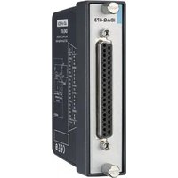
IDAQ-873-A - Module d'acquisition de données Advantech - Free user manual and instructions
Find the device manual for free IDAQ-873-A Advantech in PDF.


| Product Type | Data Acquisition Module (DAQ) |
| Brand | Advantech |
| Model | IDAQ-873-A |
| Dimensions (W x D x H) | 8.3 x 5.2 x 2.5 inches (211 x 132 x 64 mm) |
| Weight | Approximately 1.2 lbs (540 g) |
| Power Supply | +5V DC, 1.5A via external adapter or USB |
| Input Voltage Range | 0-10V analog, 0-24V digital |
| Number of Analog Inputs | 8 single-ended or 4 differential |
| Analog Input Resolution | 16-bit |
| Number of Digital I/O | 16 bidirectional |
| Sampling Rate | Up to 100 kHz |
| Communication Interface | USB 2.0 (Type B) with USB cable included |
| Compatible Software | DAQNavi, LabVIEW, MATLAB, Visual Studio |
| Operating Temperature | 0 to 70°C |
| Storage Temperature | -20 to 85°C |
| Humidity Range | 5 to 95% non-condensing |
| Isolation | 500 VDC channel-to-channel isolation |
| Maintenance | Clean with a soft, dry cloth; avoid liquids |
| Safety Precautions | Use ESD wrist strap; disconnect power before handling |
| Spare Parts / Repairability | Contact Advantech for replacement cables, connectors, and repair service |
| General Information | Designed for industrial data acquisition; includes USB cable and driver CD |
Frequently Asked Questions - IDAQ-873-A Advantech
User questions about IDAQ-873-A Advantech
0 question about this device. Answer the ones you know or ask your own.
Ask a new question about this device
Download the instructions for your Module d'acquisition de données in PDF format for free! Find your manual IDAQ-873-A - Advantech and take your electronic device back in hand. On this page are published all the documents necessary for the use of your device. IDAQ-873-A by Advantech.
USER MANUAL IDAQ-873-A Advantech
natural_image
Line drawing of an electronic circuit board with two components, one showing internal circuitry and the other a rectangular device (no text or symbols)iDAQ-871/873
Bridge Input Industrial DAQ Modules
Copyright
The documentation and the software included with this product are copyrighted 2024 by Advantech Co., Ltd. All rights are reserved. Advantech Co., Ltd. reserves the right to make improvements in the products described in this manual at any time without notice. No part of this manual may be reproduced, copied, translated, or transmitted in any form or by any means without the prior written permission of Advantech Co., Ltd. The information provided in this manual is intended to be accurate and reliable. However, Advantech Co., Ltd. assumes no responsibility for its use, nor for any infringements of the rights of third parties that may result from its use.
Acknowledgments
Intel and Pentium are trademarks of Intel Corporation.
Microsoft Windows and MS-DOS are registered trademarks of Microsoft Corp.
All other product names or trademarks are properties of their respective owners.
Product Warranty (2 years)
Advantech warrants the original purchaser that each of its products will be free from defects in materials and workmanship for two years from the date of purchase.
This warranty does not apply to any products that have been repaired or altered by persons other than repair personnel authorized by Advantech, or products that have been subject to misuse, abuse, accident, or improper installation. Advantech assumes no liability under the terms of this warranty as a consequence of such events.
Because of Advantech's high quality-control standards and rigorous testing, most customers never need to use our repair service. If an Advantech product is defective, it will be repaired or replaced free of charge during the warranty period. For out-of-warranty repairs, customers will be billed according to the cost of replacement materials, service time, and freight. Please consult your dealer for more details.
If you believe your product is defective, follow the steps outlined below.
-
Collect all the information about the problem encountered. (For example, CPU speed, Advantech products used, other hardware and software used, etc.) Note anything abnormal and list any onscreen messages displayed when the problem occurs.
-
Call your dealer and describe the problem. Please have your manual, product, and any helpful information readily available.
-
If your product is diagnosed as defective, obtain a return merchandise authorization (RMA) number from your dealer. This allows us to process your return more quickly.
-
Carefully pack the defective product, a completed Repair and Replacement Order Card, and a proof of purchase date (such as a photocopy of your sales receipt) into a shippable container. Products returned without a proof of purchase date are not eligible for warranty service.
-
Write the RMA number clearly on the outside of the package and ship the package prepaid to your dealer.
Part No. 2003087100 Edition 1
Printed in China April 2024
Declaration of Conformity
CE
This product has passed the CE test for environmental specifications when shielded cables are used for external wiring. We recommend the use of shielded cables. This type of cable is available from Advantech. Please contact your local supplier for ordering information.
Test conditions for passing also include the equipment being operated within an industrial enclosure. In order to protect the product from damage caused by electrostatic discharge (ESD) and EMI leakage, we strongly recommend the use of CE-compliant industrial enclosure products.
FCC Class A
This equipment has been tested and found to comply with the limits for a Class A digital device, pursuant to part 15 of the FCC Rules. These limits are designed to provide reasonable protection against harmful interference when the equipment is operated in a commercial environment. This equipment generates, uses, and can radiate radio frequency energy and, if not installed and used in accordance with the instruction manual, may cause harmful interference to radio communications. Operation of this equipment in a residential area is likely to cause harmful interference. In this event, users are required to correct the interference at their own expense.
Technical Support and Assistance
- Visit the Advantech website at www.advantech.com/support to obtain the latest product information.
- Contact your distributor, sales representative, or Advantech's customer service center for technical support if you need additional assistance. Please have the following information ready before calling:
– Product name and serial number
– Description of your peripheral attachments
– Description of your software (operating system, version, application software, etc.)
– A complete description of the problem
– The exact wording of any error messages
Warnings, Cautions, and Notes
Warning! Warnings indicate conditions that if not observed can cause personal injury!

Caution! Cautions are included to help prevent hardware damage and data losses. For example,

"Batteries are at risk of exploding if incorrectly installed. Do not attempt to recharge, force open, or heat the battery. Replace the battery only with the same or equivalent type as recommended by the manufacturer. Discard used batteries according to the manufacturer's instructions."
Note! Notes provide additional optional information.

Document Feedback
To assist us with improving this manual, we welcome all comments and constructive criticism. Please send all such feedback in writing to support@advantech.com.
Packing List
Before system installation, check that the items listed below are included and in good condition. If any item does not accord with the list, contact your dealer immediately.
iDAQ-871
iDAQ-871 x 1
■ Startup Manual x 1
iDAQ-873
iDAQ-873 x 1
■ Startup Manual x 1
Safety Instructions
- Read these safety instructions carefully.
- Retain this user manual for future reference.
- Disconnect the equipment from all power outlets before cleaning. Use only a damp cloth for cleaning. Do not use liquid or spray detergents.
-
For pluggable equipment, the power outlet socket must be located near the equipment and easily accessible.
-
Protect the equipment from humidity.
-
Place the equipment on a reliable surface during installation. Dropping or letting the equipment fall may cause damage.
-
The openings on the enclosure are for air convection. Protect the equipment from overheating. Do not cover the openings.
-
Ensure that the voltage of the power source is correct before connecting the equipment to a power outlet.
-
Position the power cord away from high-traffic areas. Do not place anything over the power cord.
-
All cautions and warnings on the equipment should be noted.
-
If the equipment is not used for a long time, disconnect it from the power source to avoid damage from transient overvoltage.
-
Never pour liquid into an opening. This may cause fire or electrical shock.
-
Never open the equipment. For safety reasons, the equipment should be opened only by qualified service personnel.
-
If any of the following occurs, have the equipment checked by service personnel:
– The power cord or plug is damaged.
– Liquid has penetrated the equipment.
– The equipment has been exposed to moisture.
- The equipment is malfunctioning, or does not operate according to the user manual.
– The equipment has been dropped and damaged.
– The equipment show obvious signs of breakage.
-
Do not leave the equipment in an environment with a storage temperature of below -20 ^ ( -4 ^ ) or above 60 ^ ( 140 ^ ) as this may damage the components. The equipment should be kept in a controlled environment.
-
CAUTION: Batteries are at risk of exploding if incorrectly replaced. Replace only with the same or equivalent type as recommended by the manufacturer. Discard used batteries according to the manufacturer's instructions.
-
In accordance with IEC 704-1:1982 specifications, the sound pressure level at the operator's position does not exceed 70 dB (A).
DISCLAIMER: These instructions are provided according to IEC 704-1 standards. Advantech disclaims all responsibility for the accuracy of any statements contained herein.
Safety Precautions - Static Electricity
Follow these simple precautions to protect yourself from harm and the products from damage.
To avoid electrical shock, always disconnect the power from the PC chassis before manual handling. Do not touch any components on the CPU card or other cards while the PC is powered on.
■ Disconnect the power before making any configuration changes. A sudden rush of power after connecting a jumper or installing a card may damage sensitive electronic components.
1.4 Driver Installation 3
Figure 1.3 XNavi Installation Interface.... 3
1.5 Software Utility 4
1.6 Software Development Using DAQnavi SDK 4
1.7 FPGA Code Update 4
1.8 Ordering Information 4
1.9 Accessories....4
Chapter 2 Installation Guide ....5
2.1 Initial Unpacking Check....6
2.2 Installation....6
Figure 2.1 iDAQ Module Install into iDAQ Chassis....6
2.3 Signal Connection and Pin Assignment....7
2.3.1 Quarter-Bridge Input Signal Connection....7
Figure 2.2 3-wire quarter-bridge input signal connection for iDAQ-871....7
Figure 2.3 3-wire quarter-bridge input signal connection for iDAQ-873....8
Figure 2.4 2-wire quarter-bridge input signal connection for iDAQ-871....8
Figure 2.5 2-wire quarter-bridge input signal connection for iDAQ-873....9
2.3.2 Half-Bridge Input Signal Connection....9
Figure 2.6 Half-bridge input without remote sensing signal connection....9
Figure 2.7 Half-bridge input with remote sensing signal connection 10
2.3.3 Full-Bridge Input Signal Connection .... 10 Figure 2.8 Full-bridge input without remote sensing signal connection.... 10
Figure 2.9 Full-bridge input with remote sensing signal connection 11
2.3.4 Pin Assignment.... 11
Figure 2.10 Pin Assignment Diagram of iDAQ-871 ..... 11
Table 2.1: Pin Assignment Diagram of iDAQ-871 ..... 12
Figure 2.11 Pin Assignment Diagram of iDAQ-873 12
Table 2.2: Pin Assignment Diagram of iDAQ-873 ...... 12
Chapter 3 Function Details....13
3.1 Bridge Input Overview.... 14
3.1.1 Wheatstone Bridge 14
Figure 3.1 A resistive Wheatstone bridge circuit .... 14
Figure 3.2 Ratiometric measurement ...... 15
3.1.2 Error Correction in Bridge Input Measurement.... 15
Figure 3.3 Voltage drop due to lead resistance.... 16
Figure 3.4 Remote sensing .... 16
3.2 Strain Gauge Sensor Configurations 17
3.2.1 Quarter-Bridge Configuration.... 17
Figure 3.5 Quarter-bridge configuration measuring axial and bending strain....17
3.2.2 Half Bridge Type I Configuration.... 18
Figure 3.6 Half-bridge type I configuration measuring axial and bending strain....18
3.2.3 Half Bridge Type II Configuration.... 19
Figure 3.7 Half-bridge type II configuration measuring axial and bending strain.... 19
3.2.4 Half Bridge Type III Configuration.... 20
Figure 3.8 Half-bridge type III configuration rejecting axial and measuring bending strain.... 20
3.2.5 Full Bridge Type I Configuration 21
Figure 3.9 Full-bridge type I configuration rejecting axial and measuring bending strain.... 21
3.2.6 Full-Bridge Type II Configuration.... 22
Figure 3.10 Full-bridge type II configuration rejecting axial and measuring bending strain.... 22
3.2.7 Full-Bridge Type III Configuration.... 23
Figure 3.11 Full-bridge type III configuration rejecting bending and measuring axial strain 23
3.3 Force, Pressure, and Torque Sensor Configuration 24
3.4 Analog Input Methods.... 25
3.4.1 Instant Analog Input Acquisition 25
Figure 3.12Instant analog input acquisition 25
3.4.2 Buffered Analog Input Acquisition.... 26
Figure 3.13Buffered analog input acquisition 26
Figure 3.14 Start and stop of the analog input acquisition ..... 26
Figure 3.15 Start and stop of the analog input acquisition with delay 27
3.5 Buffered Analog Input Configuration.... 27
3.5.1 One-buffered Acquisition 27
Figure 3.16Post-trigger acquisition.... 27
Figure 3.17Post-trigger acquisition with delay.... 28
Figure 3.18Pre-trigger acquisition 28
Figure 3.19 About-trigger acquisition.... 29
3.5.2 Streaming Analog Input Acquisition.... 29
Figure 3.20 Streaming acquisition 29
3.5.3 Retriggerable Analog Input Acquisition.... 30
Figure 3.21Post-trigger acquisition with retrigger 30
Figure 3.22Pre-trigger acquisition with retrigger.... 30
Figure 3.23 About-trigger acquisition with retrigger.... 30
Figure 3.24Streaming acquisition with retrigger 31
3.6 Device Description and Configuration.... 31
Figure 3.25Device Information of iDAQ-871.... 31
Appendix A Specifications....
33
A.1 Bridge Input.... 34
Table A.1: Bridge Input specification of iDAQ-871 and iDAQ-873. 34
Table A.2: Filter type in different sampling rate setting.... 34
Figure A.1 Frequency response of FIR filter under different sampling rates.... 35
Figure A.2 Frequency response of SINC1 filter under different sampling rates (16.66 SPS to 400 SPS)....35
Figure A.3 Frequency response of SINC1 filter under different sampling rates (1.2 kSPS to 7.2 kSPS).... 35
Figure A.4 Frequency response of SINC5 filter under different sampling rates 36
Table A.3: Accuracy.... 36
Table A.4: Accuracy.... 36
Table A.5: Idle Channel Noise 36
A.2 Trigger.... 37
A.3 Power Consumption.... 37
Table A.6: Power Consumption 37
A.4 General 37
A.5 Function Block.... 38
Appendix B System Dimensions ....39
B.1 System Dimensions 40
Figure B.1 System Dimensions - iDAQ-871.... 40
Figure B.2 System Dimensions - iDAQ-873.... 41
Chapter 1
Start Using iDAQ-871/873
1.1 Overview
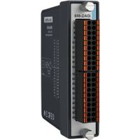
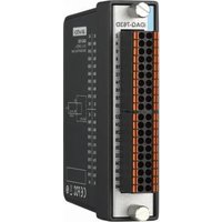
This chapter presents an overview of Advantech's industrial data acquisition (iDAQ) modules, focusing on the iDAQ-871 and iDAQ-873 models, including their product lineups, features, and accessories. Both iDAQ-871 and iDAQ-873 are 24-bit bridge type acquisition modules. The iDAQ-871 is a 4-channel acquisition module that supports various bridge inputs (full, half, and quad bridges) and offers multiple resistance and excitation voltages to accommodate different types of strain gauges. On the other hand, the iDAQ-873 is an 8-channel acquisition module designed specifically for quarter-bridge measurement. These modules are suitable for the precise measurement of strain gauges, force sensors, load cells, and similar devices.
1.2 Product Overview
iDAQ-871
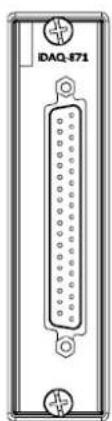
natural_image
Front panel of a device labeled IDAQ-871, showing a vertical connector with multiple pins (no readable text beyond label)
natural_image
Pure technical line drawing of a rectangular component with mounting holes and side connectors (no text or symbols)Figure 1.1 Overview of iDAQ-871
iDAQ-873
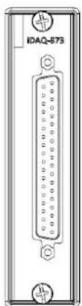
natural_image
Diagram of a vertical electronic device with labeled pins and connectors (no readable text or symbols beyond labels)
natural_image
Pure technical line drawing of a rectangular device with mounting brackets and a curved top panel (no text or symbols)Figure 1.2 Overview of iDAQ-873
1.3 Product Features
1.3.1 Power Input
The power input of all the iDAQ I/O modules come from iDAQ chassis via the DB 15-pin connector. The iDAQ I/O modules are powered on when the power of iDAQ chassis is connected.
1.3.2 BoardID
A board ID (BID) can be assigned to the iDAQ chassis by the rotary switch and slot number. The board ID will be shown in the software and can be used to distinguish modules. The number shown around the rotary switch is in hexadecimal format. For example, "A" represents 10 in decimal format, and "F" represents 15 in decimal format. The number assigned to each iDAQ module follows a rule combining the ChassisID and slot number.
1.3.3 Plug and Play Device
The iDAQ modules are hot-swappable in the iDAQ chassis. The modules will be recognized instantly in the software (Installed Devices list) when they are plugged into the iDAQ slots and they can be removed as soon as they are disabled in the software. Therefore, it's strongly recommended to operate these actions whilst the system is in idle mode not data acquisition mode.
1.4 Driver Installation
The driver package could be found on Advantech Support Portal (https://www.advantech.com/support). Search for iDAQ on the support portal, then the corresponding driver/SDK package can be found. You'll get the Xnavi installer after the download session finishes.
Execute the installer and it will guide you through the session. You can choose the device and software components you'd like to install in the system (Figure 1.3). After the selection, click on "start" to begin the installation.

Figure 1.3 Xnavi Installation Interface
1.5 Software Utility
Advantech offers device drivers, SDKs, third-party driver support and application software to help fully exploit the functions of your iDAQ system. All these software packages are available on the Advantech website: http://www.advantech.com/.
The Advantech Navigator is a utility that allows you to set up, configure and test your device, and later store your settings in a proprietary database.
-
To set up the I/O device, you could first run the Advantech Navigator program (by accessing Start/Programs/Advantech Automation/DAQNavi/Advantech Navigator). The settings could also be saved.
-
You can then view the device(s) already installed on your system (if any) on the Installed Device tree view. Once the software and hardware installation have completed, you will see the iDAQ modules in the Installed Devices list.
1.6 Software Development Using DAQNavi SDK
DAQNavi SDK is the software development kit for programming applications with Advantech DAQ products. The necessary runtime DLL, header files, software manual and tutorial videos could be installed via XNavi installer. They could be found under C:\Advantech\DAQNavi (default directory) after the finishing the installation.
1.7 FPGA Code Update
The FPGA could also be updated via the interface in Navigator. However, it isn't normal to update an FPGA. Advantech strongly suggests you to consult your technical support before considering an FPGA update.
1.8 Ordering Information
IDAQ-871-A 4-ch, 24-bit, 25.6kS/s/ch, 3-in-1 Bridge Input iDAQ Module IDAQ-873-A 8-ch, 24-bit, 25.6kS/s/ch, Quarter Bridge Input iDAQ Modul
1.9 Accessories
| PCL-10137-1E | DB-37 Shielded Cable, 1m |
| PCL-10137-2E | DB-37 Shielded Cable, 2m |
| PCL-10137-3E | DB-37 Shielded Cable, 3m |
| ADAM-3937-BE | DB-37 Wiring Terminal, DIN-rail Mount |
Chapter 2
Installation Guide
2.1 Initial Unpacking Check
Before you install your iDAQ modules, please make sure you have the following necessary components when unpacking the package:
■ DAQ module*1
■ Startup manual*1
If anything in the packing list is missing, please contact your local support for further assistance.
2.2 Installation
Below are the steps to insert the iDAQ modules into the iDAQ chassis.
- Insert the module follow the guide rail to the end
- Screw the two thumb screws tight onto the chassis

natural_image
Technical line drawing of a multi-tiered electrical enclosure with multiple cylindrical components and control panels (no text or symbols)Figure 2.1 iDAQ Module Install into iDAQ Chassis
2.3 Signal Connection and Pin Assignment
The iDAQ-871 offers a choice of three bridge completion types based on the sensor connected to the module, whereas the iDAQ-873 is specifically designed for quarter-bridge applications. Details regarding field wiring connections and pin assignments for each module are provided in the following section.
2.3.1 Quarter-Bridge Input Signal Connection
For quarter-bridge input, one of the four bridge arms serves as the external sensing element, while the other three arms are completed by the device's internal resistors. This setup is known as quarter-bridge completion. Figure 2.2 and Figure 2.3 illustrate the 3-wire quarter-bridge input signal connection for iDAQ-871 and iDAQ-873, respectively. To connect the strain gauge sensor ( R_B1 ), attach one end (1-wire side) to the EX+ terminal (EX for iDAQ-873) and the other end (2-wire side) to both the QTR/SC+ and AI+ terminals (QTR/SC and AI for iDAQ-873) using separate wires. Additionally, connect the SC- terminal to the EX- terminal for shunt calibration (applicable to iDAQ-871 only). Since remote sensing does not apply to quarter-bridge input configuration, simply connect the RS+ and RS- terminals to the EX+ and EX- terminals, respectively, on iDAQ-871. Note that the resistance of the quarter-bridge completion resistor RQB must match the nominal resistance of the strain gauge R_B1 .

flowchart
graph TD
    A["Device Internal"] --> B["ADC"]
    B --> C["V_REF"]
    D["R_LEAD"] --> E["Al+"]
    F["R_LEAD"] --> G["AI-"]
    H["R_LEAD"] --> I["RS+"]
    J["R_LEAD"] --> K["EX+"]
    L["R_B1"] --> M["QTR/SC+"]
    N["R_LEAD"] --> O["QTR/SC+"]
    P["SC-"] --> Q["RS-"]
    R["EX-"] --> S["QTR/SC+"]
    T["R_SC"] --> U["R_QB"]
    V["R_HB"] --> W["R_HB"]
    X["V_EX"] --> Y["Ground"]
    style A fill:#f9f,stroke:#333
    style B fill:#ccf,stroke:#333
    style C fill:#cfc,stroke:#333
    style D fill:#fcc,stroke:#333
    style E fill:#cff,stroke:#333
    style F fill:#ffc,stroke:#333
    style G fill:#ffc,stroke:#333
    style H fill:#ffc,stroke:#333
    style I fill:#ffc,stroke:#333
    style J fill:#ffc,stroke:#333
    style K fill:#ffc,stroke:#333
    style L fill:#ffc,stroke:#333
    style M fill:#ffc,stroke:#333
    style N fill:#ffc,stroke:#333
    style O fill:#ffc,stroke:#333
    style P fill:#ffc,stroke:#333
    style Q fill:#ffc,stroke:#333
    style R fill:#ffc,stroke:#333
    style S fill:#ffc,stroke:#333
    style T fill:#ffc,stroke:#333
    style U fill:#ffc,stroke:#333
    style V fill:#ffc,stroke:#333
    style W fill:#ffc,stroke:#333
    style X fill:#ffc,stroke:#333
Figure 2.2 3-wire quarter-bridge input signal connection for iDAQ-871

Figure 2.3 3-wire quarter-bridge input signal connection for iDAQ-873
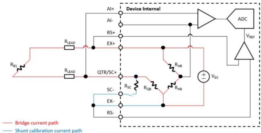
2-wire quarter-bridge input can also be used, as shown in Figure 2.4 and Figure 2.5. One wire is used to connect both QTR/SC+ and Al+ terminals (QTR/SC and Al for iDAQ-873). However, shunt calibration in this configuration will results in more error due to imbalance of lead wire resistance ( R_LEAD ).
flowchart
graph TD
    A["Device Internal"] --> B["ADC"]
    B --> C["V_REF"]
    D["R_B1"] --> E["R_LEAD"]
    E --> F["QTR/SC+"]
    G["R_S"] --> H["QTR/SC+"]
    I["EX-"] --> J["QTR/SC+"]
    K["RS+"] --> L["Device Internal"]
    M["AI+"] --> N["Device Internal"]
    O["AI-"] --> P["Device Internal"]
    Q["RS+"] --> R["Device Internal"]
    S["EX+"] --> T["Device Internal"]
    U["R_SC"] --> V["Shunt calibration current path"]
    W["R_QB"] --> X["Shunt calibration current path"]
    Y["R_HB"] --> Z["Shunt calibration current path"]
    AA["V_EX"] --> AB["Shunt calibration current path"]
    AC["Bridge current path"] --> AD["Shunt calibration current path"]
Figure 2.4 2-wire quarter-bridge input signal connection for iDAQ-871

Figure 2.5 2-wire quarter-bridge input signal connection for iDAQ-873
2.3.2 Half-Bridge Input Signal Connection
For half-bridge input, two of the four bridge arms are external sensing elements, hence the name. The other two arms are provided, or completed, by device's internal resistors. This configuration is also called half-bridge completion.
Figure 2.6 shows half-bridge input without remote sensing signal connection. Connect one end of the strain gauge sensor ( R_B1 ) to EX+ terminal, and the other end ( R_B2 ) to both EX- and SC- terminals using different wires. In addition, connect the middle node (junction of R_B1 and R_B2 ) of the strain gauge sensor to both Al+ and QTR/SC+ terminals using different wires. Since remote sensing is not used in this configuration, simply connect RS+ and RS- terminals to EX+ and EX- terminals, respectively.

flowchart
graph TD
    subgraph_Device_Internal["Device Internal"]
        A1["AI+"] --> B1["ADC"]
        A2["AI-"] --> B1
        A3["RS+"] --> B1
        A4["EX+"] --> B1
        B1 --> C1["V_REF"]
        D1["R_LEAD"] --> E1["R_B1"]
        D2["R_LEAD"] --> E2["R_B2"]
        D3["R_LEAD"] --> E3["R_LEAD"]
        D4["R_LEAD"] --> E4["R_LEAD"]
        D5["R_LEAD"] --> E5["R_LEAD"]
        D6["R_LEAD"] --> E6["R_LEAD"]
        D7["R_LEAD"] --> E7["R_LEAD"]
        D8["R_LEAD"] --> E8["R_LEAD"]
        D9["R_LEAD"] --> E9["R_LEAD"]
        D10["R_LEAD"] --> E10["R_LEAD"]
        D11["R_LEAD"] --> E11["R_LEAD"]
        D12["R_LEAD"] --> E12["R_LEAD"]
        D13["R_LEAD"] --> E13["R_LEAD"]
        D14["R_LEAD"] --> E14["R_LEAD"]
        D15["R_LEAD"] --> E15["R_LEAD"]
        D16["R_LEAD"] --> E16["R_LEAD"]
        D17["R_LEAD"] --> E17["R_LEAD"]
        D18["R_LEAD"] --> E18["R_LEAD"]
        D19["R_LEAD"] --> E19["R_LEAD"]
        D20["R_LEAD"] --> E20["R_LEAD"]
        D21["R_LEAD"] --> E21["R_LEAD"]
        D22["R_LEAD"] --> E22["R_LEAD"]
        D23["R_LEAD"] --> E23["R_LEAD"]
        D24["R_LEAD"] --> E24["R_LEAD"]
        D25["R_LEAD"] --> E25["R_LEAD"]
        D26["R_LEAD"] --> E26["R_LEAD"]
        D27["R_LEAD"] --> E27["R_LEAD"]
        D28["R_LEAD"] --> E28["R_LEAD"]
        D29["R_LEAD"] --> E29["R_LEAD"]
        D30["R_LEAD"] --> E30["R_LEAD"]
        D31["R_LEAD"] --> E31["R_LEAD"]
        D32["R_LEAD"] --> E32["R_LEAD"]
        D33["R_LEAD"] --> E33["R_LEAD"]
        D34["R_LEAD"] --> E34["R_LEAD"]
        D35["R_LEAD"] --> E35["R_LEAD"]
        D36["R_LEAD"] --> E36["R_LEAD"]
        D37["R_LEAD"] --> E37["R_LEAD"]
        D38["R_LEAD"] --> E38["R_LEAD"]
        D39["R_LEAD"] --> E39["R_LEAD"]
        D40["R_LEAD"] --> E40["R_LEAD"]
        D41["R_LEAD"] --> E41["R_LEAD"]
        D42["R_LEAD"] --> E42["R_LEAD"]
        D43["R_LEAD"] --> E43["R_LEAD"]
        D44["R_LEAD"] --> E44["R_LEAD"]
        D45["R_LEAD"] --> E45["R_LEAD"]
        D46["R_LEAD"] --> E46["R_LEAD"]
        D47["R_LEAD"] --> E47["R_LEAD"]
        D48["R_LEAD"] --> E48["R_LEAD"]
        D49["R_LEAD"] --> E49["R_LEAD"]
        D50["R_LEAD"] --> E50["R_LEAD"]
    end
    style Device_Internal fill:#f9f,stroke:#333
    style Device_Internal fill:#ccf,stroke:#333
    style Device_Internal fill:#cfc,stroke:#333
    style Device_Internal fill:#fcc,stroke:#333
    style Device_Internal fill:#ffc,stroke:#333
    style Device_Internal fill:#cff,stroke:#333
    style Device_Internal fill:#ffc,stroke:#333
    style Device_Internal fill:#ffc,stroke:#333
    style Device_Internal fill:#ffc,stroke:#333
    style Device_Internal fill:#ffc,stroke:#333
    style Device_Internal fill:#ffc,stroke:#333
    style Device_Internal fill:#ffc,stroke:#333
    style Device_Internal fill:#ffc,stroke:#333
    style Devices_Internal fill:#ffc,stroke:#333
Figure 2.6 Half-bridge input without remote sensing signal connection
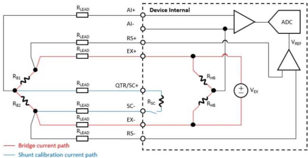
If remote sensing is required, connect the RS+ terminal to one end of the strain gauge ( R_B1 ) by an independent wire, and connect the RS- terminal to the other end ( R_B2 ) by another independent wire, as shown in Figure 2.7 Do not share the same wire for RS and EX terminals.
flowchart
graph TD
    subgraph_Device_Internal["Device Internal"]
        A1["R_LEAD"] --> B1["AI+"]
        A2["R_LEAD"] --> B2["RS+"]
        A3["R_LEAD"] --> B3["EX+"]
    end
    subgraph_ADC["ADC"]
        C1["ADC"] --> D1["V_REF"]
    end
    E1["R_B1"] --> F1["R_LEAD"]
    E2["R_B2"] --> F2["R_LEAD"]
    E3["R_LEAD"] --> F3["R_LEAD"]
    E4["R_LEAD"] --> F4["R_LEAD"]
    E5["R_LEAD"] --> F5["R_LEAD"]
    E6["R_LEAD"] --> F6["R_LEAD"]
    E7["R_LEAD"] --> F7["R_LEAD"]
    E8["R_LEAD"] --> F8["R_LEAD"]
    E9["R_LEAD"] --> F9["R_LEAD"]
    E10["R_LEAD"] --> F10["R_LEAD"]
    E11["R_LEAD"] --> F11["R_LEAD"]
    E12["R_LEAD"] --> F12["R_LEAD"]
    E13["R_LEAD"] --> F13["R_LEAD"]
    E14["R_LEAD"] --> F14["R_LEAD"]
    E15["R_LEAD"] --> F15["R_LEAD"]
    E16["R_LEAD"] --> F16["R_LEAD"]
    E17["R_LEAD"] --> F17["R_LEAD"]
    E18["R_LEAD"] --> F18["R_LEAD"]
    E19["R_LEAD"] --> F19["R_LEAD"]
    E20["R_LEAD"] --> F20["R_LEAD"]
    E21["R_LEAD"] --> F21["R_LEAD"]
    E22["R_LEAD"] --> F22["R_LEAD"]
    E23["R_LEAD"] --> F23["R_LEAD"]
    E24["R_LEAD"] --> F24["R_LEAD"]
    E25["R_LEAD"] --> F25["R_LEAD"]
    E26["R_LEAD"] --> F26["R_LEAD"]
    E27["R_LEAD"] --> F27["R_LEAD"]
    E28["R_LEAD"] --> F28["R_LEAD"]
    E29["R_LEAD"] --> F29["R_LEAD"]
    E30["R_LEAD"] --> F30["R_LEAD"]
    E31["R_LEAD"] --> F31["R_LEAD"]
    E32["R_LEAD"] --> F32["R_LEAD"]
    E33["R_LEAD"] --> F33["R_LEAD"]
    E34["R_LEAD"] --> F34["R_LEAD"]
    E35["R_LEAD"] --> F35["R_LEAD"]
    E36["R_LEAD"] --> F36["R_LEAD"]
    E37["R_LEAD"] --> F37["R_LEAD"]
    E38["R_LEAD"] --> F38["R_LEAD"]
    E39["R_LEAD"] --> F39["R_LEAD"]
    E40["R_LEAD"] --> F40["R_LEAD"]
    E41["R_LEAD"] --> F41["R_LEAD"]
    E42["R_LEAD"] --> F42["R_LEAD"]
    E43["R_LEAD"] --> F43["R_LEAD"]
    E44["R_LEAD"] --> F44["R_LEAD"]
    E45["R_LEAD"] --> F45["R_LEAD"]
    E46["R_LEAD"] --> F46["R_LEAD"]
    E47["R_LEAD"] --> F47["R_LEAD"]
    E48["R_LEAD"] --> F48["R_LEAD"]
    E49["R_LEAD"] --> F49["R_LEAD"]
    E50["R_LEAD"] --> F50["R_LEAD"]
    E51["R_LEAD"] --> F51["R_LEAD"]
    E52["R_LEAD"] --> F52["R_LEAD"]
    E53["R_LEAD"] --> F53["R_LEAD"]
    E54["R_LEAD"] --> F54["R_LEAD"]
    E55["R_LEAD"] --> F55["R_LEAD"]
    E56["R_LEAD"] --> F56["R_LEAD"]
    E57["R_LEAD"] --> F57["R_LEAD"]
    E58["R_LEAD"] --> F58["R_LEAD"]
    E59["R_LEAD"] --> F59["R_LEAD"]
    E60["R_LEAD"] --> F60["R_ROB"]
    E61["R_ROB"] --> G["+ - V_EX"]

    style Device_Internal fill:#f9f,stroke:#333
    style ADC fill:#ccf,stroke:#333
    style BridgeCurrentPath stroke-dasharray: 5 5
    note right of BridgeCurrentPath
        Red line = BridgeCurrentPath
        Blue line = ShuntCalibrationCurrentPath
        Legend: Red line = BridgeCurrentPath
        Legend: Blue line = ShuntCalibrationCurrentPath
Figure 2.7 Half-bridge input with remote sensing signal connection
2.3.3 Full-Bridge Input Signal Connection
For full-bridge input, all four bridge arms are external sensing elements, hence the name. This configuration is also called full-bridge completion.
Figure 2.8 shows full-bridge input without remote sensing signal connection. Connect middle node of the two left arms (junction of R_B1 and R_B2 ) to both Al+ and QTR/SC+ terminals using different wires, and middle node of the two right arms (junction of R_B4 and R_B3 ) to Al- terminal. Connect the middle node of the two upper arms (junction of R_B1 and R_B4 ) to EX+ terminal, and the middle node of the two lower arms (junction of R_B2 and R_B3 ) to both EX- and SC- terminals using different wires. Since remote sensing is not used in this configuration, simply connect RS+ and RS- terminals to EX+ and EX- terminals, respectively.

flowchart
graph TD
    subgraph_Device_Internal["Device Internal"]
        direction TB
        A["R_LEAD"] --> B["AI+"]
        C["R_LEAD"] --> D["AI-"]
        E["R_LEAD"] --> F["RS+"]
        G["R_LEAD"] --> H["EX+"]
        I["R_LEAD"] --> J["QTR/SC+"]
        K["R_LEAD"] --> L["SC-"]
        M["R_LEAD"] --> N["EX-"]
        O["R_LEAD"] --> P["RS-"]
        Q["Device"] --> R["ADC"]
        S["Shunt"] --> T["V_REF"]
        U["Bridge current path"] --> V["Ground"]
    end
    style Device_Internal fill:#f9f,stroke:#333
    style Device_Internal fill:#ccf,stroke:#333
    style Bridge currents stroke:#ff0000,stroke-width:2px
    style Shunt currents stroke:#ff0000,stroke-width:2px
Figure 2.8 Full-bridge input without remote sensing signal connection
If remote sensing is required, connect RS+ terminal to the middle point of the two upper arms ( R_B1 and R_B4 ) by an independent wire, and connect the RS- terminal to the middle point of the two lower arms ( R_B2 and R_B3 ) by another independent wire, as shown in Figure 2.9. Do not share the same wire for RS and EX terminals.

flowchart
graph TD
    subgraph_Device_Internal["Device Internal"]
        direction TB
        A["Device"] --> B["ADC"]
        B --> C["V_REF"]
        D["R_LEAD"] --> E["Al+"]
        F["R_LEAD"] --> G["Al-"]
        H["R_LEAD"] --> I["RS+"]
        J["R_LEAD"] --> K["EX+"]
    end
    subgraph QTR/SC["QTR/SC+"]
        L["R_LEAD"] --> M["SC-"]
        N["R_LEAD"] --> O["EX-"]
        P["R_LEAD"] --> Q["RS-"]
    end
    subgraph_Shunt_Calibration_Calibration["Shunt calibration current path"]
        R["Bridge current path"] --> S["Ground"]
        T["Shunt calibration current path"] --> U["Ground"]
    end
    style Device_Internal fill:#f9f,stroke:#333
    style QTR/SC fill:#ccf,stroke:#333
    style Shunt_Calibration_Calibration fill:#cfc,stroke:#333
Figure 2.9 Full-bridge input with remote sensing signal connection
2.3.4 Pin Assignment
iDAQ-871

other
| Label | Value | |---|---| | EXO+ | 37 | | AIO+ | 36 | | AIO- | 35 | | EXO- | 34 | | EX1+ | 33 | | AI1+ | 32 | | AI1- | 31 | | EX1- | 30 | | NC | 29 | | NC | 28 | | EX2+ | 27 | | AI2+ | 26 | | AI2- | 25 | | EX2- | 24 | | EX3+ | 23 | | AI3+ | 22 | | AI3- | 21 | | EX3- | 20 | | RS0- | 19 | | RS0+ | 18 | | QTR/SC0+ | 17 | | SC0- | 16 | | NC | 15 | | RS1- | 14 | | RS1+ | 13 | | QTR/SC1+ | 12 | | SC1- | 11 | | NC | 10 | | RS2- | 9 | | RS2+ | 8 | | QTR/SC2+ | 7 | | SC2- | 6 | | NC | 5 | | RS3- | 4 | | RS3+ | 3 | | QTR/SC3+ | 2 | | SC3- | 1 |Figure 2.10 Pin Assignment Diagram of iDAQ-871
Table 2.1: Pin Assignment Diagram of iDAQ-871
| Pin Name Pin Number Description | ||
| RS<0..3>+ 3, 8, 13, 18 Remote sensing positive terminal. | ||
| RS<0..3>- 4, 9, 14, 19 Remote sensing negative terminal. | ||
| EX<0..3>+ 23, 27, 33, 37 Excitation voltage positive terminal. | ||
| EX<0..3>- 20, 24, 30, 34 Excitation voltage negative terminal. | ||
| AI<0..3>+ 22, 26, 32, 36 Analog input positive terminal. | ||
| AI<0..3>- 21, 25, 31, 35 Analog input negative terminal. | ||
| QTR/SC<0..3>+ 2, 7, 12, 17 | Quarter bridge completion/shunt calibrationpositive terminal. | |
| SC<0..3>- 1, 6, 11, 16 Shunt calibration negative terminal. | ||
| NC | 5, 10, 15, 28, 29 | Not connected. |
iDAQ-873

other
| Category | Value | |---|---| | AI0 | 19 | | NC | 18 | | EX4 | 17 | | QTR/SC4 | 16 | | NC | 15 | | AI1 | 14 | | NC | 13 | | EX5 | 12 | | QTR/SC5 | 11 | | EX2 | 10 | | QTR/SC2 | 9 | | NC | 8 | | AI6 | 7 | | NC | 6 | | EX3 | 5 | | QTR/SC3 | 4 | | NC | 3 | | AI7 | 2 | | | 1 | | EX0 | | | QTR/SC0 | | | NC | | | AI4 | | | NC | | | EX1 | | | QTR/SC1 | | | NC | | | AI5 | | | NC | | | AI2 | | | NC | | | EX6 | | | QTR/SC6 | | | NC | | | AI3 | | | NC | | | EX7 | | | QTR/SC7 | |Figure 2.11 Pin Assignment Diagram of iDAQ-873
Table 2.2: Pin Assignment Diagram of iDAQ-873
| Pin Name | Pin Number | Description |
| QTR/SC<0...7> | 18, 13, 27, 22, 34, 29, 6, 1 | Quarter bridge completion/shunt calibration terminal of Al |
| EXn<0...7> | 19, 14, 28, 23, 35, 30, 7, 2 | Excitation voltage terminal of Al |
| Al<0...7> | 37, 32, 9, 4, 16, 11, 25, 20 | Terminal of analog input channel |
| NC | 3, 5, 8, 10, 12, 15, 17, 21, 24,26, 31, 33, 36 | No Connection |
Chapter 3
Function Details
3.1 Bridge Input Overview
This section gives a brief introduction to the architecture and operation of the bridge input circuit, which is also called a Wheatstone bridge. In addition, there are several methods to correct the error in bridge input measurement, including remote sensing, offset nulling, and shunt calibration, are described.
3.1.1 Wheatstone Bridge
Many sensors, including strain gauges, load cells, pressure sensors, and torque sensors are based on the concept of a Wheatstone bridge. A Wheatstone bridge contains four elements or arms. Although these elements can be resistive or reactive, they are however almost resistive for sensors previously mentioned.

chemical
Electrical circuit diagram with resistors and voltage sourceFigure 3.1 A resistive Wheatstone bridge circuit
Figure 3.1 shows a resistive Wheatstone bridge circuit. It consists of an excitation voltage source and two voltage dividers. R_B1 and R_B2 form one voltage divider, and R_B4 and R_B3 form the other voltage divider. The excitation voltage ( V_EX ) is connected to the upper node (junction of R_B1 and R_B4 ) and the lower node (junction of R_B2 and R_B3 ), and output voltage ( V_O ) is measured between the middle node of two voltage dividers. When R_B1 = R_B2 and R_B3 = R_B4 , the output voltage is 0 V.
If some of the resistors are replaced by active sensors, whose resistance change with the physical quantity, V_O will also change due to these resistance changes. By measuring the value of this voltage change, the physical quantity can be calculated.
There are three types of active sensor configuration in bridge input circuit: quarter-bridge, half-bridge, and full-bridge. Refer to Figure 3.1, for quarter-bridge, only R_B1 is an active sensor; for half-bridge, both R_B1 and R_B2 are active sensors; for full-bridge, all four resistors are active sensors.
Due to the property of the voltage divider, V_O will be proportional to V_EX . When VEX is used as the voltage reference of an ADC, and V_O is measured by the ADC, as shown in Figure 3.2, the measurement result is an unitless ratio between V_O and V_EX , or V_O/V_EX . For specified resistances, the measurement result is independent of the variation in V_EX . This is called ratiometric measurement.

Figure 3.2 Ratiometric measurement
3.1.2 Error Correction in Bridge Input Measurement
Field wiring is used to connect sensors to measurement devices that have a non-zero resistance, and resistance of each bridge arm also has errors. These undesired factors create errors in bridge input measurement. The device provides mechanisms to correct the errors: remote sensing, offset nulling, and shunt calibration.
3.1.2.1 Remote Sensing
Remote sensing corrects for errors due to resistance of excitation voltage leads. It is useful in applications that employ long or small wires to connect the sensors to the measuring device, as the wires have high resistance.
As shown in Figure 3.3, current generated by excitation voltage source will flow through the positive terminal of the source, the bridge, to the negative terminal of the source (indicated by red lines). The wire resistance ( R_LEAD ) that connects both positive terminal and negative terminal of the source to the bridge causes voltage drops ( V_LEAD ), which results in a smaller voltage across the bridge compared to the actual excitation voltage generated by the source. This voltage difference leads to gain reduction in the measured result.

Figure 3.3 Voltage drop due to lead resistance
As shown in Figure 3.4, instead of using excitation voltage source output as the voltage reference of the ADC, in remote sensing, two additional wires (indicated by green lines) that connect to the bridge directly measure the voltage across the bridge, and use this value as the voltage reference of the ADC. Because both lines are high impedance input terminals, there is no current flowing through, and therefore no voltage drops on these wires.
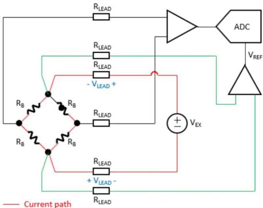
Figure 3.4 Remote sensing
Remote sensing is not applicable for quarter-bridge configuration due to the imbalance architecture (only R_B1 has wire resistance).
3.1.2.2 Offset Nulling
In fact, output of the bridge may not be 0 V even when not loaded. This is because slight variations in resistance among the bridge arms generate nonzero offset voltage. Offset nulling performs software compensation for this offset voltage.
The software will first measure the bridge output when not loaded and stored it as an initial value. Then this initial value will be subtracted from the reading before scaling when measuring under load.
3.1.2.3 Shunt Calibration
In shunt calibration, load is simulated by shunting a shunt calibration resistor ( R_sc ) inside the device to R_B2 of the bridge, which results in equivalent resistance change on that arm. A switch inside the device controls whether to connect R_sc or not. Because values of all resistors are known, and the resistance change on the shunting arm is also known, the theoretical value of this simulated load can therefore be calculated. Then the bridge output when shunting is measured, and the ratio between the theoretical value and the measured value is stored and used when scaling the reading.
3.2 Strain Gauge Sensor Configurations
This section describes the supported strain gauge sensor configurations.
3.2.1 Quarter-Bridge Configuration
This section provides information for the quarter-bridge strain gauge sensor configuration. This configuration measures either axial or bending strain. Figure 3.5 shows how to position the strain gauge sensor in both axial and bending configurations. Refer to 2.3.1 Quarter-Bridge Input Signal Connection for detailed signal wiring of this configuration.

Figure 3.5 Quarter-bridge configuration measuring axial and bending strain
■ The quarter-bridge configuration has the following characteristics:
A single active strain gauge sensor R_B1 is mounted in the principal direction of axial or bending strain.
■ Sensitive to both axial and bending strain.
A quarter-bridge completion resistor R_QB and two half-bridge completion resistors R_HB are required. They are provided by the device.
■ Both a shunt calibration resistor R_SC and a switch are provided by the device.
■ Sensitivity ≈ 0.5 μV/V per με, for GF = 2.0.
■ Strain value can be calculated by the following equation:
$$ \text { strain } (\varepsilon) \quad \frac {- 4 V _ {r}}{G F 1 + (2 V _ {r}} $$
where GF is the gauge factor of the strain gauge sensor provided by the sensor manufacturer, Vr is the ratiometric bridge output value measured by the ADC
$$ V _ {r} = \frac {V _ {A I} (\text {strained}) - V _ {A I} (\text {unstrained})}{V _ {E X}} $$
■ Shunt calibration can be used to compensate for errors due to lead resistance.
3.2.2 Half Bridge Type I Configuration
This section provides information for the half-bridge type I strain gauge sensor configuration. This configuration measures either axial or bending strain. Figure 3.6 shows how to position the strain gauge sensors in both axial and bending configurations. Refer to 2.3.2 Half-Bridge Input Signal Connection for detailed signal wiring of this configuration.


Figure 3.6 Half-bridge type I configuration measuring axial and bending strain
The half-bridge type I configuration has the following characteristics:
One active strain gauge sensor R_B1 measuring the strain and one dummy strain gauge sensor R_B2 for temperature compensation. R_B1 is mounted in the principal direction of axial or bending strain. R_B2 is mounted in close thermal contact with the strain specimen but bonded to the specimen, and is usually mounted perpendicular to the principal axis of strain.
■ Sensitive to both axial and bending strain.
■ Two half-bridge completion resistor R_HB are required. They are provided by the device.
■ Both a shunt calibration resistor R_SC and a switch are provided by the device.
■ Sensitivity ≈ 0.5 μV/V per με, for GF = 2.0.
■ Strain value can be calculated by the following equation:
$$ \text { strain } (\varepsilon) \quad \frac {- 4 V _ {r}}{G F 1 + (2 V _ {r}} $$
where GF is the gauge factor of the strain gauge sensor provided by the sensor manufacturer, Vr is the ratiometric bridge output value measured by the ADC
$$ V _ {r} = \frac {V _ {A I} (\text { strained }) - V _ {A I} (\text { unstrained })}{V _ {E X}} $$
■ Shunt calibration can be used to compensate for errors due to lead resistance.
3.2.3 Half Bridge Type II Configuration
This section provides information for the half-bridge type II strain gauge sensor configuration. This configuration measures either axial or bending strain. Figure 3.7 shows how to position the strain gauge sensors in both axial and bending configurations. Refer to 2.3.2 Half-Bridge Input Signal Connection for detailed signal wiring of this configuration.
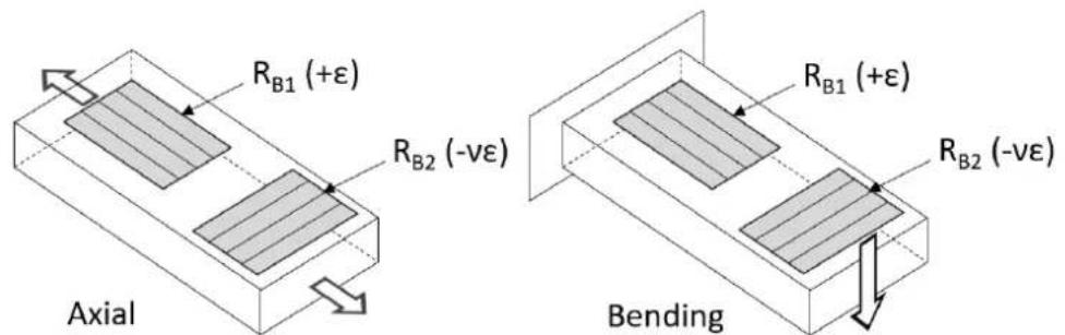
Figure 3.7 Half-bridge type II configuration measuring axial and bending strain
The half-bridge type II configuration has the following characteristics:
There are two active strain gauge sensors R_B1 and R_B2 . R_B1 measures the strain and is mounted in the principal direction of axial or bending strain. R_B2 acts as a Poisson gauge and is perpendicular to the principal axis of strain.
■ Sensitive to both axial and bending strain.
■ Two half-bridge completion resistor R_HB are required. They are provided by the device.
■ Both a shunt calibration resistor R_SC and a switch are provided by the device.
■ Sensitivity ≈ 0.65 μV/V per με, for GF = 2.0.
■ Strain value can be calculated by the following equation:
$$ \text { strain } (\varepsilon) = \frac {- 4 V _ {r}}{G F [ 1 + (v - 1) \mathbb {Z} (v - 1) ]} $$
where GF is the gauge factor of the strain gauge sensor provided by the sensor manufacturer, v is the Poisson's ratio, defined as the negative ratio of transverse strain to axial (longitudinal) strain. Poisson's ratio is a material property of the specimen being measured, and Vr is the ratiometric bridge output value measured by the ADC
$$ V _ {r} = \frac {V _ {A I} (\text {strained}) - V _ {A I} (\text {unstrained})}{V _ {E X}} $$
■ Shunt calibration can be used to compensate for errors due to lead resistance.
3.2.4 Half Bridge Type III Configuration
This section provides information for the half-bridge type III strain gauge sensor configuration. This configuration only measures bending strain. Figure 3.8 shows how to position the strain gauge sensors in bending configuration. Refer to 2.3.2 Half-Bridge Input Signal Connection for detailed signal wiring of this configuration.

Figure 3.8 Half-bridge type III configuration rejecting axial and measuring bending strain
The half-bridge type III configuration has the following characteristics:
There are two active strain gauge sensors R_B1 and R_B2 . RB1 is mounted in the principal direction of bending strain on one side of the strain specimen (top) while R_B2 is mounted in the principal direction of bending strain on the opposite side (bottom).
■ Sensitive to bending strain and rejects axial strain.
■ Two half-bridge completion resistor R_HB are required. They are provided by the device.
■ Both a shunt calibration resistor R_SC and a switch are provided by the device.
■ Sensitivity ≈ 1 μV/V per με, for GF = 2.0.
■ Strain value can be calculated by the following equation:
$$ \text { strain } (\varepsilon) \quad \frac {- 2 V _ {r}}{G F} = $$
where GF is the gauge factor of the strain gauge sensor provided by the sensor manufacturer, and Vr is the ratiometric bridge output value measured by the ADC
$$ V _ {r} \quad \frac {V _ {A I} (\text { strained }) - V _ {A I} (\text { unstrained })}{V _ {E X}} $$
■ Shunt calibration can be used to compensate for errors due to lead resistance.
3.2.5 Full Bridge Type I Configuration
This section provides information for the full-bridge type I strain gauge sensor configuration. This configuration only measures bending strain. Figure 3.9 shows how to position the strain gauge sensors in bending configuration. Refer to 2.3.3 Full-Bridge Input Signal Connection for detailed signal wiring of this configuration.
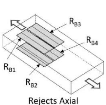

Figure 3.9 Full-bridge type I configuration rejecting axial and measuring bending strain
The full-bridge type I configuration has the following characteristics:
There are four active strain gauge sensors R_B1 , R_B2 , R_B3 , and R_B4 . R_B1 and R_B3 are mounted in the principal direction of bending strain on one side of the strain specimen (top) while R_B2 and R_B4 are mounted in the principal direction of bending strain on the opposite side (bottom).
■ Highly sensitive to bending strain and rejects axial strain.
■ Both a shunt calibration resistor R_SC and a switch are provided by the device.
■ Sensitivity ≈ 2 μV/V per με, for GF = 2.0.
■ Strain value can be calculated by the following equation:
$$ \text { strain } (\varepsilon) \quad \frac {- V _ {r}}{G F} = $$
where GF is the gauge factor of the strain gauge sensor provided by the sensor manufacturer, and Vr is the ratiometric bridge output value measured by the ADC
$$ V _ {r} = \frac {V _ {A I} (\text { strained }) - V _ {A I} (\text { unstrained })}{V _ {E X}} $$
■ Shunt calibration can be used to compensate for errors due to lead resistance.
3.2.6 Full-Bridge Type II Configuration
This section provides information for the full-bridge type II strain gauge sensor configuration. This configuration only measures bending strain. Figure 3.10 shows how to position the strain gauge sensors in bending configuration. Refer to 2.3.3 Full-Bridge Input Signal Connection for detailed signal wiring of this configuration.

Figure 3.10 Full-bridge type II configuration rejecting axial and measuring bending strain
The full-bridge type II configuration has the following characteristics:
There are four active strain gauge sensors R_B1 , R_B2 , R_B3 , and R_B4 . R_B1 and R_B2 are mounted in the principal direction of bending strain with R_B1 on one side of the strain specimen (top) while R_B2 on the opposite side (bottom). R_B3 and R_B4 act together as Poisson gauge and are mounted transverse (perpendicular) to the principal direction of bending strain with R_B4 on one side of the strain specimen (top) and R_B3 on the opposite side (bottom).
■ Sensitive to bending strain and rejects axial strain.
■ Both a shunt calibration resistor R_SC and a switch are provided by the device.
■ Sensitivity ≈ 1.3 μV/V per με, for GF = 2.0.
■ Strain value can be calculated by the following equation:
$$ \text { strain } (\varepsilon) \quad \frac {- 2 V _ {r}}{G F (1 + v)} = $$
where GF is the gauge factor of the strain gauge sensor provided by the sensor manufacturer, v is the Poisson's ratio, defined as the negative ratio of transverse strain to axial (longitudinal) strain. Poisson's ratio is a material property of the specimen being measured, and Vr is the ratiometric bridge output value measured by the ADC
$$ V _ {r} = \frac {V _ {A l} (\text {strained}) - V _ {A l} (\text {unstrained})}{V _ {E X}} $$
■ Shunt calibration can be used to compensate for errors due to lead resistance.
3.2.7 Full-Bridge Type III Configuration
This section provides information for the full-bridge type III strain gauge sensor configuration. This configuration only measures axial strain. Figure 3.11 shows how to position the strain gauge sensors in axial configuration. Refer to 2.3.3 Full-Bridge Input Signal Connection for detailed signal wiring of this configuration.

Measures Axial

Rejects Bending
Figure 3.11 Full-bridge type III configuration rejecting bending and measuring axial strain
The full-bridge type III configuration has the following characteristics:
There are four active strain gauge sensors R_B1 , R_B2 , R_B3 , and R_B4 . R_B1 and R_B3 are mounted in the principal direction of bending strain with R_B3 on one side of the strain specimen (top) while R_B1 on the opposite side (bottom). R_B2 and R_B4 act together as Poisson gauge and are mounted transverse (perpendicular) to the principal direction of bending strain with R_B4 on one side of the strain specimen (top) and R_B2 on the opposite side (bottom).
■ Sensitive to axial strain and rejects bending strain.
■ Both a shunt calibration resistor R_SC and a switch are provided by the device.
■ Sensitivity ≈ 1.3 μV/V per με, for GF = 2.0.
■ Strain value can be calculated by the following equation:
$$ \operatorname{strain} (\varepsilon) = \frac {- 2 V _ {r}}{G F [ (v + 1) - V _ {r} (v - 1) ]} $$
where GF is the gauge factor of the strain gauge sensor provided by the sensor manufacturer, v is the Poisson's ratio, defined as the negative ratio of transverse strain to axial (longitudinal) strain. Poisson's ratio is a material property of the specimen being measured, and Vr is the ratiometric bridge output value measured by the ADC
$$ V _ {r} = \frac {V _ {A l} (\text {strained}) - V _ {A l} (\text {unstrained})}{V _ {E X}} $$
■ Shunt calibration can be used to compensate for errors due to lead resistance.
3.3 Force, Pressure, and Torque Sensor Configuration
The device can be used with force sensors (such as load cells), pressure sensors, or torque sensor that have the following characteristics:
■ Wheatstone bridge based.
■ Unamplified mV/V or V/V output.
These sensors typically use a full-bridge configuration with a 350Ω nominal bridge resistance, but other configurations and nominal bridge resistances also can be used. Refer to 2.3.3 Full-Bridge Input Signal Connection for detailed signal wiring of this configuration.
In Advantech DAQNavi, linear scaling for bridge-based force, pressure, and torque sensors is based on two points which are specified as pairs of corresponding physical and electrical values: "EV 1 , PV 1 ", and "EV 2 , PV 2 ". These should be based on the calibration certificate of the sensor, if one is available; otherwise, they can be based on the specifications or datasheet of the sensor. Any two points can be used assuming that they are far enough apart to accurately determine the slop of the linear scaling equation. For example:
■ PV 1: The zero point of the sensor. Zero force, zero pressure, or zero torque.
EV 1: The electrical output (ratiometric bridge output) corresponding to the zero point of the sensor, in mV/V or V/V.
PV 2: The maximum physical reading of the sensor, or capacity. Maximum load, maximum pressure, or maximum torque.
EV 2: The electrical output (ratiometric bridge output) corresponding to the maximum physical reading of the sensor, in mV/V or V/V.
Note! Some sensor calibration certificates specify the electrical output in mV or V, not mV/V or V/V. If this is the case, divide the specified electrical output by the excitation voltage at which the calibration was performed.
The two-point linear conversion uses the following equations:
$$ m \quad \frac {P V _ {1} - P V _ {2}}{E V _ {1} - E V _ {2}} = $$
$$ b = P V _ {1} - m \times E V _ {1} $$
$$ \text { Physical reading } = m \times V _ {r} + b $$
where Vr is the ratiometric bridge output value measured by the ADC.
3.4 Analog Input Methods
3.4.1 Instant Analog Input Acquisition
With instant analog input acquisition, the software controls the sample timing. The analog-to-digital converter (ADC) is continuously converting analog input signals by its maximum allowable conversion rate. Each time the software sends a “read instant analog input sample” command, the most recent conversion result is sampled as shown in Figure 3.12.

line
| Parameter | Value | | ------------------- | --------- | | Software Polling | 1.5 V | | Instant AI Sample | 2.5 V | | Software Polling | 0.7 V |Figure 3.12 Instant analog input acquisition
The advantage of instant acquisition is low latency. It is typically used for reading a single sample of analog input.
3.4.2 Buffered Analog Input Acquisition
With buffered analog input acquisition, the ADC conversion rate and the duration of the acquisition is controlled by hardware timing signals. All conversion results are sampled and stored in the buffer memory before sending back to the host computer as shown in Figure 3.13.

line
| Input | Waveform Description | | ------------ | ---------------------------- | | Analog Input 0 | Broad peak | | Analog Input 1 | Broad peak | | Analog Input 2 | Broad peak | | Sample Clock | Square wave pattern | | AI Sample in FIFO | Al2, Al1, Al0 segments labeled 'AI2' | | Sample Clock | Square wave pattern | | Sample Clock | Al2, Al1, Al0 segments labeled 'AI1' | | Sample Clock | Al0, Al1, Al0 segments labeled 'AI0' |Figure 3.13 Buffered analog input acquisition
The start and stop of the acquisition are controlled by the start trigger and stop trigger, respectively. When configuration is completed, the acquisition engine of the iDAQ chassis is at standby state. After receiving a start trigger, acquisition becomes active and each rising edge of the sample clock acquires one analog input sample. The acquisition active period lasts until a stop trigger is received, which ends the acquisition. This is shown in Figure 3.14.

Figure 3.14 Start and stop of the analog input acquisition
The start and stop of acquisition can also be delayed in number of samples after receiving the corresponding trigger signal. As shown in Figure 3.15, the start of acquisition is delayed by 3 samples after receiving a start trigger, and the stop of acquisition is delayed by 2 samples after receiving a stop trigger.
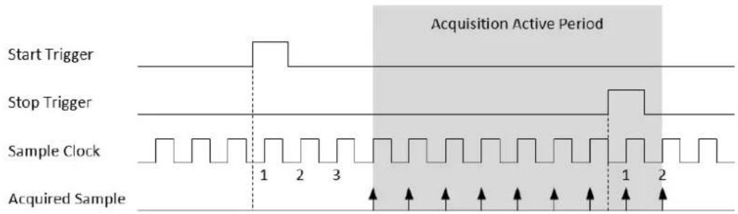
Figure 3.15 Start and stop of the analog input acquisition with delay
Buffered analog input acquisition has several advantages over instant analog input acquisition:
The start and stop time of acquisition (or duration of the acquisition) can be precisely controlled by hardware trigger signals.
■ ADC conversion rate is configurable, and sample rate can be much higher by using hardware sample clock signal.
■ Time between samples is deterministic.
3.5 Buffered Analog Input Configuration
3.5.1 One-buffered Acquisition
For one-buffered acquisition, only a specified number of samples is acquired. The start or stop of acquisition can be controlled by a software command or a hardware signal. Three types of acquisitions can be achieved: post-trigger acquisition, pre-trigger acquisition, and about-trigger acquisition.
3.5.1.1 Post-Trigger Acquisition
A post-trigger acquisition acquires a specified number of samples after the start trigger. The acquisition starts when a start trigger is received and automatically stops when the specified number of samples is acquired. An example of 5-sample post-trigger acquisition is shown in Figure 3.16.

Figure 3.16 Post-trigger acquisition
The start trigger can be a software command or a hardware signal. If a hardware signal is used as the start trigger, the start of acquisition can be delayed for a specified number of sample clock cycles after a start trigger is received. Figure 3.17 shows an example of a 2-sample delay post-trigger acquisition. Refer to the device specifications for possible signal sources.
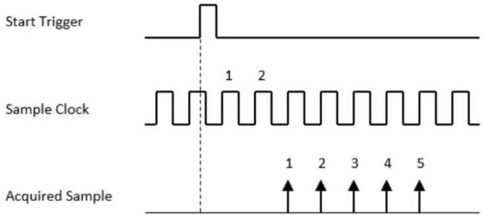
Figure 3.17 Post-trigger acquisition with delay
3.5.1.2 Pre-Trigger Acquisition
A pre-trigger acquisition acquires a specified number of samples before the stop trigger. The acquisition is started by a software command and stopped when a hardware stop trigger is received. Figure 3.18 shows an example of a 5-sample pre-trigger acquisition. Only the samples in the shaded area are returned.
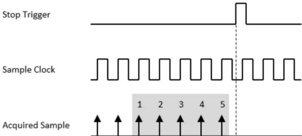
Figure 3.18 Pre-trigger acquisition
The stop trigger can only be a hardware signal. Refer to the device specifications for possible signal sources.
3.5.1.3 About-Trigger Acquisition
An about-trigger acquisition is the same as a pre-trigger acquisition except that the time when the acquisition stops can be delayed by a specified number of sample clock cycles. Figure 3.19 shows an example of a 5-sample about-trigger acquisition with 2 cycles of stop delay. Only the samples in the shaded area are returned.

Figure 3.19 About-trigger acquisition
The stop trigger can only be a hardware signal. Refer to the device specifications for possible signal sources.
3.5.2 Streaming Analog Input Acquisition
For a streaming acquisition, the number of samples to be acquired is set to infinite. The acquisition starts when a start trigger is received and continues until a stop trigger is received as shown in Figure 3.20.
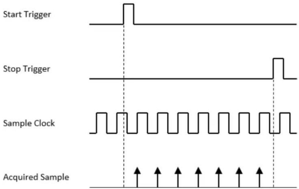
Figure 3.20 Streaming acquisition
Both the start trigger and the stop trigger can come from a software command or a hardware signal. If a hardware signal is used, the start (for the start trigger) or the stop (for the stop trigger) of the acquisition can also be delayed. Refer to the device specifications for possible signal sources.
3.5.3 Retriggerable Analog Input Acquisition
The acquisition can be re-triggerable. When re-trigger is enabled, after the acquisition stops, it restarts whenever the required trigger is received, and reconfiguration of the acquisition is not required.
Figures 3.21 to 3.24 show examples of retrigger acquisition for post-trigger, pre-trigger, about-trigger, and streaming acquisitions, respectively. In a post-trigger acquisition, a start trigger is ignored while the acquisition is in progress. In an about-trigger acquisition, a stop trigger is ignored while the acquisition is being stopped.

Figure 3.21 Post-trigger acquisition with retrigger

Figure 3.22 Pre-trigger acquisition with retrigger

Figure 3.23 About-trigger acquisition with retrigger

Figure 3.24 Streaming acquisition with retrigger
3.6 Device Description and Configuration
The Device Description is used to differentiate the modules in the iDAQ system. It's given following a naming rule of combining chassis ID, model name and slot number. You can change the description in Navigator, or just leave it as default. The description is used in your own program, in order to get control or device handler from the device.
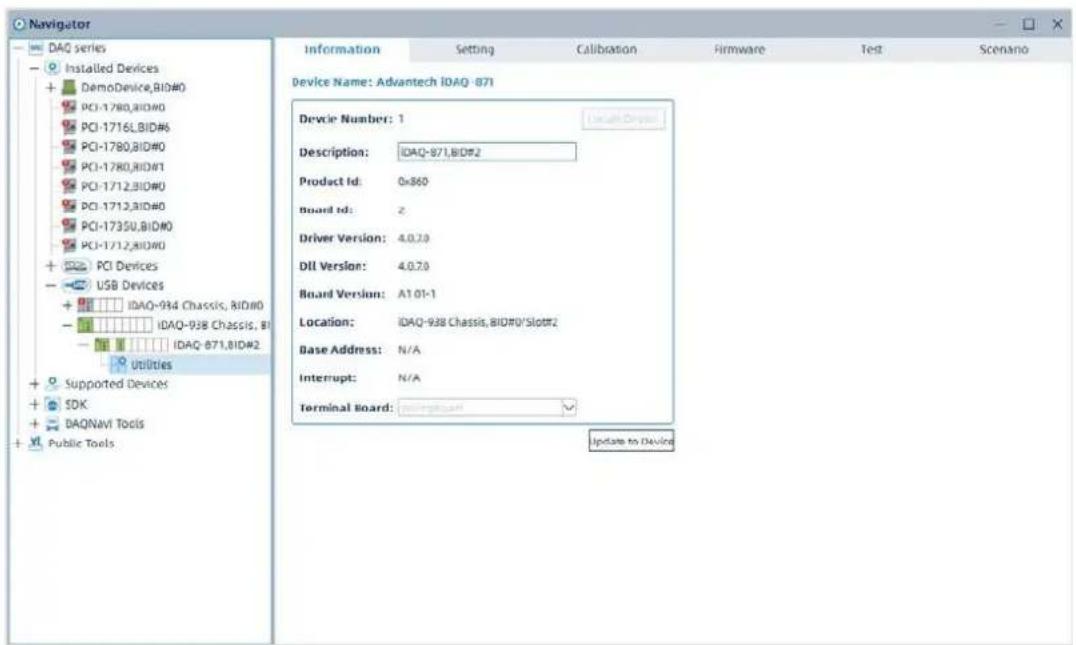
Figure 3.25 Device Information of iDAQ-871
Appendix
A
Specifications
A.1 Bridge Input
Table A.1: Bridge Input specification of iDAQ-871 and iDAQ-873
| Item iDAQ-871 iDAQ-873 | ||
| ADC Resolution 24-bit | ||
| Channels 4 8 | ||
| Input Range | ±1 V/V, ±500 mV/V, ±250 mV/V, ±125 mV/V, ±62.5 mV/V, ±31.25 mV/V, ±15.63 mV/V, or ±7.81 mV/VAuto configured by software according to physical input range settings | |
| Bridge Mode Full, half, quarter | Quarter | |
| Bridge Resistance | 120 Ω, 350 Ω, 1 kΩ | 120 Ω |
| Shunt Calibration | 100 kΩ | 100 kΩ |
| Excitation Voltage | 2.5V, 5V | 2V |
■ Digital low-pass filter
- Filter type: FIR or SINC1, selected by sampling rate. Refer to Table A2 for detailed information
Table A.2: Filter type in different sampling rate setting
| Sampling Rate (SPS) | -3-dB Bandwidth (Hz) | Filter Type |
| 2.5 | 1.2 | FIR |
| 5 | 2.4 | FIR |
| 10 | 4.7 | FIR |
| 16.6 | 7.38 | SINC1 |
| 20 | 13 | FIR |
| 50 | 22.1 | SINC1 |
| 60 | 26.6 | SINC1 |
| 100 | 44.3 | SINC1 |
| 400 | 177 | SINC1 |
| 1200 | 525 | SINC1 |
| 2400 | 1015 | SINC1 |
| 4800 | 1798 | SINC1 |
| 7200 | 2310 | SINC1 |
| 14400 | 2940 | SINC5 |
| 19200 | 3920 | SINC5 |
| 25600 | 5227 | SINC5 |
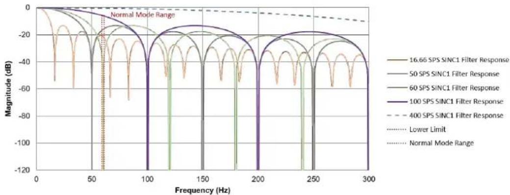
-3 dB bandwidth: Configured along with sampling rate. Refer to Figure A1\~A4 for detailed frequency response for each filters under different sampling rate settings.
Digital Filter Frequency Response

line
| Frequency (Hz) | 2.5 SPS FIR Filter Response | 5 SPS FIR Filter Response | 10 SPS FIR Filter Response | 20 SPS FIR Filter Response | | -------------- | --------------------------- | ------------------------- | -------------------------- | -------------------------- | | 0 | 0 | 0 | 0 | 0 | | 10 | -20 | -25 | -30 | -35 | | 20 | -40 | -45 | -50 | -55 | | 30 | -60 | -65 | -70 | -75 | | 40 | -80 | -85 | -90 | -95 | | 50 | -100 | -105 | -110 | -115 | | 60 | -120 | -125 | -130 | -135 | | 70 | -80 | -85 | -90 | -95 | | 80 | -60 | -65 | -70 | -75 | | 90 | -40 | -45 | -50 | -55 | | 100 | -20 | -25 | -30 | -35 |Figure A.1 Frequency response of FIR filter under different sampling rates
Digital Filter Frequency Response
line
| Frequency (Hz) | 16.66 SPS SINC1 Filter Response | 50 SPS SINC1 Filter Response | 60 SPS SINC1 Filter Response | 100 SPS SINC1 Filter Response | 400 SPS SINC1 Filter Response | Lower Limit | Normal Mode Range | | -------------- | ------------------------------ | ---------------------------- | ---------------------------- | ----------------------------- | ----------------------------- | ----------- | ----------------- | | 0 | 0 | 0 | 0 | 0 | 0 | 0 | 0 | | 50 | -20 | -20 | -20 | -20 | -20 | -20 | -20 | | 100 | -40 | -40 | -40 | -40 | -40 | -40 | -40 | | 150 | -60 | -60 | -60 | -60 | -60 | -60 | -60 | | 200 | -80 | -80 | -80 | -80 | -80 | -80 | -80 | | 250 | -100 | -100 | -100 | -100 | -100 | -100 | -100 | | 300 | -120 | -120 | -120 | -120 | -120 | -120 | -120 |Figure A.2 Frequency response of SINC1 filter under different sampling rates (16.66 SPS to 400 SPS)
Digital Filter Frequency Response

line
| Frequency (Hz) | 1200 SPS SINCI Filter Response | 2400 SPS SINCI Filter Response | 4800 SPS SINCI Filter Response | 7200 SPS SINCI Filter Response | | -------------- | ------------------------------ | ------------------------------ | ------------------------------ | ------------------------------ | | 0 | 0 | 0 | 0 | 0 | | 500 | -10 | -15 | -20 | -25 | | 1000 | -30 | -40 | -50 | -60 | | 1500 | -60 | -70 | -90 | -110 | | 2000 | -80 | -90 | -120 | -140 | | 2500 | -100 | -110 | -150 | -170 | | 3000 | -110 | -120 | -160 | -180 | | 3500 | -120 | -130 | -170 | -190 | | 4000 | -130 | -140 | -180 | -200 |Figure A.3 Frequency response of SINC1 filter under different sampling rates (1.2 kSPS to 7.2 kSPS)
Digital Filter Frequency Response

line
| Frequency (Hz) | 14.4kSPS SINCS Filter Response | 19.2kSPS SINCS Filter Response | 25.6kSPS SINCS Filter Response | | -------------- | ------------------------------ | ------------------------------ | ------------------------------ | | 0 | 0 | 0 | 0 | | 4000 | -5 | -8 | -10 | | 6000 | -15 | -20 | -25 | | 8000 | -30 | -35 | -40 | | 10000 | -50 | -55 | -60 | | 12000 | -75 | -70 | -85 | | 14000 | -100 | -65 | -105 |Figure A.4 Frequency response of SINC5 filter under different sampling rates
Isolation protection: 600 V _DC , Channel to FGND
Accuracy
Operating temperature within ±5^ of last, system-calibration temperature ( 25^ )
Table A.3: Accuracy
| ±1 V/V ±500mV/V ±250mV/V ±125mV/V ±62.5mV/V ±31.25 mV/V ±15.63 mV/V ±7.81 mV/V | |||
| Calibrated Typ. | Gain | ±0.05% ±0.05% | |
| Offset | |||
| Non-Cali-brated Typ. | Gain | ±0.10% ±0.20% | |
| Offset | |||
Out of calibration temperature ±5°C of last
Table A.4: Accuracy
| ±1 V/V | ±500m V/V | ±250mV/V ±1 | 25m V/V | ±62.5m V/V | ±31.25 mV/V | ±15.63 mV/V | ±7.81 mV/V | ||
| Calibrated Typ. | Gain ±0. | 20% ±0. | 20% ±0.20% | ±0.20% ±0. | 20% ±0.20% | ±0.20% ±0 | 20% | ||
| Offset ±0. | 25% ±0. | 25% ±0.25% | ±0.25% ±0. | 25% ±0.25% | ±0.25% ±0. | 25% | |||
| Non-calibrated Typ. | Gain ±0. | 60% ±0. | 60% ±0.60% | ±0.60% ±0. | 70% ±0.70% | ±0.70% ±0 | 70% | ||
| Offset ±0. | 30% ±0. | 30% ±0.30% | ±0.30% ±0. | 35% ±0.35% | ±0.35% ±0. | 35% | |||
DC Performance
Table A.5: Idle Channel Noise
| Range | 10 S/s 1.2 kS/s 25.6 kS/s | |||||
| Noise (μVRMS) | Effective Resolution (bits) | Noise( μVRMS) | Effective Resolution (bits) | Noise (μVRMS) | Effective Resolution (bits) | |
| ±1 V/V | 0.45 | 24.00 | 4.96 | 20.94 | 33.6 | 18.17 |
| ±0.5V/V | 0.31 | 23.94 | 3.92 | 20.28 | 21.4 | 17.83 |
| ±0.25 V/V | 0.15 | 23.99 | 1.44 | 20.72 | 10.6 | 17.81 |
| ±0.125 V/V | 0.056 | 24 | 0.73 | 20.70 | 4.3 | 18.14 |
| ±62.5 mV/V | 0.045 | 23.72 | 0.50 | 20.23 | 2.77 | 17.78 |
| ±31.25 mV/V | 0.028 | 23.4 | 0.27 | 20.10 | 1.53 | 17.63 |
| ±15.625 mV/V | 0.031 | 22.26 | 0.24 | 19.31 | 1.34 | 16.83 |
| ±7.8125 mV/V | 0.022 | 21.75 | 0.24 | 18.3 | 1.14 | 16.05 |
■ Shunt calibration
- Resistance: 100 k
- Resistance accuracy: ±0.1% max.
- Resistance drift: ±100 ppm/°C max.
■ Over-voltage protection: ±30 V
■ Acquisition type: Instant or buffered, software configurable
■ Buffered acquisition
- Enabled channel combination: Each channel can be enabled/disabled independently by software
- Sample clock rate: 25.6 kHz max., for all channels, simultaneous sampling, software configurable
– Sample clock source: From chassis - Allowable internal sample clock rate: 50 MHz/n, where n is an integer larger than 1,953, software configurable
- Internal data buffer (FIFO) size: 1,024 samples
A.2 Trigger
■ Number of triggers: 2 max., selectable via software
■ Trigger action: Start, delay to start, stop, or delay to stop
■ Trigger delay range: 0 \~ 16,777,215 samples
■ Sample number: 0 \~ 16,777,215 samples
A.3 Power Consumption
Table A.6: Power Consumption
| Typical Maximum |
| iDAQ-871 0.8W 2.1W |
| iDAQ-873 2W 2.6W |
A.4 General
■ Form factor: iDAQ Module
■ Dimension: 100 x 80 x 25 mm (3.94 x 3.15 x 0.98 in.)
Weight: 175 g
I/O connector:37-pin D-SUB
■ Operating temperature: -40 °C to 70 °C (-40 °F to 158 °F)
■ Storage temperature: -40 °C to 85 °C (-40 °F to 185 °F)
■ Operating humidity: Up to 90% RH, non-condensing
■ Storage humidity: Up to 95% RH, non-condensing
■ Vibration: 5Grms, Random Vibration
Shock: 30G
- Indoor use only
A.5 Function Block
iDAQ-871

flowchart
graph LR
    A["EX+"] --> B["Resistor"]
    C["AI+"] --> D["Switch"]
    E["AI-"] --> F["Inverter"]
    G["QTR/SC+"] --> H["Resistor"]
    I["SC-"] --> J["Switch"]
    K["EX-"] --> L["Inverter"]
    M["RS+"] --> N["Inverter"]
    O["RS-"] --> P["Inverter"]
    Q["ADC"] --> R["FPGA"]
    S["iDAQ-871"] --> T["FPGA"]
    U["iDAQ-871"] --> V["DB15"]
    W["Isolation"] --> X["+"]
    Y["+"] --> Z["Ground"]
iDAQ-873

flowchart
graph TD
    A["EXC"] --> B["OPA"]
    C["AI"] --> B
    D["RC"] --> B
    B --> E["ADC"]
    E --> F["FPGA"]
    F --> G["iDAQ-873"]
    H["DB15"] --> I["Output"]
    style B fill:#f9f,stroke:#333
    style E fill:#ccf,stroke:#333
    style F fill:#cfc,stroke:#333
    style G fill:#fcc,stroke:#333
Appendix B
System Dimensions
B.1 System Dimensions
iDAQ-871
natural_image
Technical line drawing of a vertical mechanical component with a 70.0mm dimension label (no other text or symbols)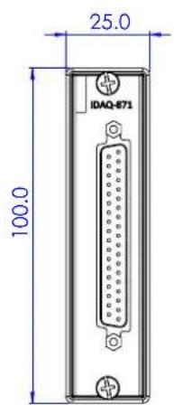

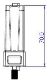
Figure B.1 System Dimensions - iDAQ-871
iDAQ-873

Figure B.2 System Dimensions - iDAQ-873
www.advantech.com
Please verify specifications before quoting. This guide is intended for reference purposes only.
All product specifications are subject to change without notice.
No part of this publication may be reproduced in any form or by any means, such as electronically, by photocopying, recording, or otherwise, without prior written permission from the publisher.
All brand and product names are trademarks or registered trademarks of their respective companies.
© Advantech Co., Ltd. 2024


- iDAQ-871/873
- Bridge Input Industrial DAQ Modules
- Copyright
- Acknowledgments
- Product Warranty (2 years)
- Declaration of Conformity
- CE
- FCC Class A
- Technical Support and Assistance
- Warnings, Cautions, and Notes
- Document Feedback
- Packing List
- iDAQ-871
- iDAQ-873
- Safety Instructions
- Safety Precautions - Static Electricity
- Chapter 2 Installation Guide ....5
- Chapter 3 Function Details....13
- Appendix A Specifications....
- Appendix B System Dimensions ....39
- Chapter 1
- Overview
- Product Overview
- Product Features
- Power Input
- BoardID
- Plug and Play Device
- Driver Installation
- Software Utility
- Software Development Using DAQNavi SDK
- FPGA Code Update
- Ordering Information
- Accessories
- Chapter 2
- Initial Unpacking Check
- Installation
- Signal Connection and Pin Assignment
- Quarter-Bridge Input Signal Connection
- Half-Bridge Input Signal Connection
- Full-Bridge Input Signal Connection
- Pin Assignment
- Chapter 3
- Bridge Input Overview
- Wheatstone Bridge
- Error Correction in Bridge Input Measurement
- Remote Sensing
- Offset Nulling
- Shunt Calibration
- Strain Gauge Sensor Configurations
- Quarter-Bridge Configuration
- Half Bridge Type I Configuration
- Half Bridge Type II Configuration
- Half Bridge Type III Configuration
- Full Bridge Type I Configuration
- Full-Bridge Type II Configuration
- Full-Bridge Type III Configuration
- Force, Pressure, and Torque Sensor Configuration
- Analog Input Methods
- Instant Analog Input Acquisition
- Buffered Analog Input Acquisition
- Buffered Analog Input Configuration
- One-buffered Acquisition
- Post-Trigger Acquisition
- Pre-Trigger Acquisition
- About-Trigger Acquisition
- Streaming Analog Input Acquisition
- Retriggerable Analog Input Acquisition
- Device Description and Configuration
- Appendix
- A
- A.1 Bridge Input
- ■ Digital low-pass filter
- DC Performance
- ■ Shunt calibration
- ■ Over-voltage protection: ±30 V
- ■ Acquisition type: Instant or buffered, software configurable
- ■ Buffered acquisition
- A.2 Trigger
- A.3 Power Consumption
- A.4 General
- A.5 Function Block
- Appendix B
- B.1 System Dimensions
- www.advantech.com
Brand : Advantech
Model : IDAQ-873-A
Category : Module d'acquisition de données