XP480SE30001 - SSD Drive SEAGATE - Free user manual and instructions
Find the device manual for free XP480SE30001 SEAGATE in PDF.

| Product Type | SSD Drive |
| Brand | Seagate |
| Model | XP480SE30001 |
| Capacity | 480 GB |
| Form Factor | 2.5-inch |
| Interface | SATA III (6 Gb/s) |
| Sequential Read Speed | Up to 540 MB/s |
| Sequential Write Speed | Up to 520 MB/s |
| Dimensions (L x W x H) | 100.2 mm x 69.85 mm x 7 mm |
| Weight | Approx. 50 g |
| Operating Temperature | 0°C to 70°C |
| Storage Temperature | -40°C to 85°C |
| Power Consumption (Active) | 2 W typical |
| Power Consumption (Idle) | 0.5 W typical |
| Shock Tolerance (Operating) | 1500 G / 0.5 ms |
| MTBF | 1.5 million hours |
| Warranty | Limited 3-year |
| Compatibility | Windows, macOS, Linux |
| Special Features | TRIM support, S.M.A.R.T., Error Correction |
Frequently Asked Questions - XP480SE30001 SEAGATE
User questions about XP480SE30001 SEAGATE
0 question about this device. Answer the ones you know or ask your own.
Ask a new question about this device
Download the instructions for your SSD Drive in PDF format for free! Find your manual XP480SE30001 - SEAGATE and take your electronic device back in hand. On this page are published all the documents necessary for the use of your device. XP480SE30001 by SEAGATE.
USER MANUAL XP480SE30001 SEAGATE
natural_image
Abstract geometric logo with orange and gray triangular shapes (no text or symbols)NYTRO™
Seagate® Nytro® 4350 NVMe SSD
Product Manual
User Capacity Model Number
480 GB XP480SE30001
960 GB XP960SE30001
1920 GB XP1920SE30001
205237900, Rev B
December 2023
© 2023, Seagate Technology LLC All rights reserved. Publication number: 205237900, Rev B, December 2023.
Seagate Technology reserves the right to make changes to the product(s) or information disclosed herein at any time without notice. No part of this publication may be reproduced in any form without written permission of Seagate Technology LLC. Call 877-PUB-TEK1(877-782-8351) to request permission.
Seagate, Seagate Technology and the Spiral logo are registered trademarks of Seagate Technology LLC in the United States and/or other countries. Nytro, and SeaTools are either trademarks or registered trademarks of Seagate Technology LLC or one of its affiliated companies in the United States and/or other countries. All other trademarks or registered trademarks are the property of their respective owners.
The NVMe word mark and/or NVMExpress design mark are trademarks of NVMExpress, Inc. The PCIe word mark and/or PCIExpress design mark are registered trademarks and/or service marks of PCI-SIG.
When referring to drive capacity, one gigabyte, or GB, equals one billion bytes and one terabyte, or TB, equals one trillion bytes. Your computer's operating system may use a different standard of measurement and report a lower capacity. In addition, some of the listed capacity is used for formatting and other functions, and thus will not be available for data storage. Actual quantities will vary based on various factors, including file size, file format, features and application software. Actual data rates may vary depending on operating environment and other factors. The export or re-export of hardware or software containing encryption may be regulated by the U.S. Department of Commerce, Bureau of Industry and Security (for more information, visit www.bis.doc.gov), and controlled for import and use outside of the U.S.
Contents
Seagate Technology Support Services 5
1. Introduction ...... 6
2. Specifications 8
2.1 Models and Capacity 8
2.2 Performance 8
2.3 Latency 9
2.4 Quality of Service (QoS) 9
2.5 Supply Voltage 10
2.6 Power Consumption 10
2.7 Environmental Conditions 11
2.8 Reliability and Endurance 12
3. Mechanical Information 13
3.1 Dimensions and Weight 13
4. Pin and Signal Descriptions .... 15
5. SMART Support 18
5.1 SMART IDs 18
6. Feature Details 20
6.1 Flash Management 20
6.1.1 Error Correction Code (ECC) 20
6.1.2 Wear Leveling 20
6.1.3 Bad Block Management 20
6.1.4 TRIM 20
6.1.5 SMART 20
6.1.6 Over Provisioning 21
6.1.7 Firmware Upgrade 21
6.1.8 Thermal Throttling 21
6.1.9 Multiple Namespaces 21
6.1.10 Garbage Collection 21
6.2 Advanced Device Security Features 22
6.2.1 Secure Erase 22
6.2.2 Physical Presence SID 22
6.2.3 Sanitize 22
6.3 SSD Lifetime Management 22
6.3.1 Media Wear Indicator 23
6.3.2 Read Only Mode (End of Life) 23
6.4 Adaptive Approach to Performance Tuning 23
6.4.1 Predict and Fetch 23
6.4.2 Throughput 23
7. Safety Certifications, and Compliance 24
7.1 Regulatory Model Numbers 24
8. Installation Precautions ...... 25
8.1 Handling Precautions 25
8.2 Assembly Precautions 25
Seagate Technology Support Services
For Internal SSD Support, visit: https://www.seagate.com/support/products/
For Firmware Download and Tools Download for Secure Erase, visit: https://www.seagate.com/support/downloads/
For information regarding online support and services, visit: http://www.seagate.com/contacts/
For information regarding Warranty Support, visit: http://www.seagate.com/support/warranty-and-replacements/
For information regarding data recovery services, visit:
http://www.seagate.com/services-software/seagate-recovery-services/recover/
For Seagate OEM and Distribution partner and Seagate reseller portal, visit: http://www.seagate.com/partners
1. Introduction
The Seagate® Nytro® 4350 SSD is a fast, dependable storage solution for boot applications or read-intensive workloads in data centers. The Seagate Nytro 4350 SSD offers PCIe Gen 4 x 4 interface with NVMe™ protocol support in a small M.2 form factor.
Table 1 The Nytro 4350 SSD Features
| Feature Description | ||
| Capacity (User) | ■ 480 GB, 960 GB, 1920 GB | |
| Certifications, Eco-Compliance | ■ CE, UL, FCC, BSMI, KCC, Microsoft WHQL, VCCI, CB■ RoHS | |
| Dimensions | ■ M.2 2280: 80 mm ( ± 0.15) x 22 mm ( ± 0.15) x 4 mm ( ± 0.08) | |
| Endurance | ■ 1 Drive Writes Per Day (DWPD) Endurance rating | valid for SSD Life Remaining >1% (SMART E7h>1).SeeSection 2.8, Reliability and Endurance. |
| Form Factor | ■ M.2 2280 | |
| Interface Compliance | ■ NVMe 1.4■ PCI Express Base 4.0■ PCIe Gen 4 x 4 lane & backward compatible to PCIe Gen 3, Gen 2, and Gen 1■ 8 IO queues supported (1 admin queue and 8 IO queue). Each IO queue support 256 entries. | |
| NAND | ■ eTLC | |
| Operating Systems | ■ Windows® 11 Pro (64 bit), Windows Server 2019, 2022 (64 bit)■ Ubuntu 20.04■ CentOS 8 | |
| Performance Random | ■ Read: Up to 800,000 IOPS■ Write: Up to 58,000 IOPS | Actual performance might vary depending on use conditions and environment.SeeSection 2.2, Performance. |
| Performance Sequential | ■ Read: Up to 5500MB/s■ Write: Up to 2000MB/s | Actual performance might vary depending on the capacity, use conditions and environment.SeeSection 2.2, Performance. |
| Power Consumption | ■ Active mode: < 11.5W■ Idle mode: < 3.3W | Results vary with capacity and mode.SeeSection 2.6, Power Consumption. |
| Power Management | ■ Supports Active State Power Management (ASPM) | |
| Power Loss Data Protection | ■ In-process writes to the NAND are completed in the event of an unexpected power loss | |
| Reliability | ■ End-to-end data path protection■ MTBF: 2 million hours■ UBER: 1 error in 10^17 bits read | |
| Security | ■ TCG Pyrite 2.0 | |
Table 1 The Nytro 4350 SSD Features
| Feature Description | ||
| Shock and Vibration | Shock■ Non-Operating: 1,500 G, at 0.5 ms | See Section 2.7, Environmental Conditions. |
| Vibration■ Non-Operating: 1.52 G_RMS , (20 to 800 Hz, Frequency) | ||
| Temperature Range (Operating) | ■ 0°C to 70°C■ Temperature Sensor (SMART Attribute ID C2h) | |
| Voltage | ■ Min = 3.14V■ Max = 3.47V | |
| Warranty | Five years, or when the device reaches Host TBW, whichever happens first. Endurance rating valid for SSD Life Remaining > 1% (SMART E7h>1). | |
| Weight | ■ 9.7 to 10.5g | |
2. Specifications
2.1 Models and Capacity
Table 2 Models and Capacity
| Capacity Model | User Addressable Sectors | |
| 480 GB XP480SE30001 937,703,088 | ||
| 960 GB XP960SE30001 1,875,385,008 | ||
| 1920 GB XP1920SE30001 3,750,748,848 |
NOTE About capacity:
■ Sector Size: 512 Bytes
■ User-addressable LBA count = (97696368) + (1953504 x (Desired Capacity in Gb-50.0)). From International Disk Drive Equipment and Materials Association (IDEMA) (LBA1-03_standard.doc)
2.2 Performance
Table 3 Random and Sequential Read and Write Performance
| Parameter 480 GB | 960 GB | 1920 GB | |
| 128KB Sequential Read (MB/s) | 5500 | 5500 | 5500 |
| 128KB Sequential Write (MB/s) 700 | 1400 | 2000 | |
| 4KB Random Read (IOPS) | 400,000 | 600,000 | 800,000 |
| 4KB Random Write (IOPS) | 17,000 | 34,000 | 58,000 |
| 8KB Random Read (IOPS) | 230,000 | 330,000 | 460,000 |
| 8KB Random Write (IOPS) | 9,000 | 18,000 | 30,000 |
NOTE About performance:
- Performance can vary based on the SSD's firmware version, system hardware, and configuration.
■ Performance is measured with the following conditions
(a) Sustained Sequential: FIO, full-range, QD=32
(b) Sustained Random: FIO, full-range, QD=32, 8 workers
2.3 Latency
Table 4 QD1 4KB Random Average Latency
| Capacity Read (4KB) Write (4KB) | |
| 480 GB 75 40 | |
| 960 GB 75 30 | |
| 1920 GB 75 30 | |
NOTE About latency:
■ Performance can differ according to flash configuration and platform.
■ Units are in microseconds.
2.4 Quality of Service (QoS)
Table 5 Quality of Service (QoS)
| Capacity | QoS (99%) | |||
| Read(4KB QD=1) | Write(4KB QD=1) | Read(4KB QD=32) | Write(4KB QD=32) | |
| Unit: μs | ||||
| 480 GB | 100 | 60 | 350 | 1600 |
| 960 GB | 100 | 50 | 300 | 970 |
| 1920 GB | 100 | 50 | 250 | 850 |
| Capacity | QoS (99.99%) | |||
| Read(4KB QD=1) | Write(4KB QD=1) | Read(4KB QD=32) | Write(4KB QD=32) | |
| Unit: μs | ||||
| 480 GB | 130 | 130 | 550 | 1500 |
| 960 GB | 130 | 130 | 550 | 1300 |
| 1920 GB | 130 | 130 | 450 | 1100 |
NOTE About QoS:
■ QoS is measured with the following conditions
FIO test: 4KB transfer size, QD=1 or 32 on 4KB random read and write workload on whole LBA range of SSD performance on steady state and all background operations run normally.
- According to random 4KB QD=1 and 32 workloads, the result of QoS is the maximum round-trip time which is taken for 99.0% and 99.99% of commands to host.
■ QoS can vary based on SSD's firmware version, system hardware and configuration.
2.5 Supply Voltage
Table 6 Supply Voltage
| Parameter Rating | |
| Operating Voltage | Min = 3.14VMax = 3.47V |
| Rise Time (Max/Min) | 100 ms / 0.1 ms |
| Fall Time (Max/Min) | 1 s / 10 ms |
| Minimum Off Time | 1 s |
NOTE Minimum Off Time is the time between power being removed from the SSD (Vcc<100 mW) and power being reapplied to the SSD.
2.6 Power Consumption
Table 7 Power Consumption
| 480 GB 960 GB 1920 GB | ||
| Active Read (RMS, Max) 9.4W 10.4W 11.5W | ||
| Active Write (RMS, Max) 6.3W 8.1W 10.7W | ||
| Idle | 3.3W 3.3W 3.3W |
NOTE About power consumption:
■ The measured power voltage is 3.3 V.
■ Power consumption is measured during the sequential/random read and write performed by FIO on Linux.
■ Power Consumption can vary based on SSD's firmware version, system hardware and configuration.
2.7 Environmental Conditions
Table 8 Temperature, Humidity, Shock
| Specification Value | |
| TemperatureOperational temperature(with airflow: 800 LFM at 35°C)Non-operating | 0°C to 70°C-40°C to 85°C |
| HumidityOperatingNon-operating (storage) | 90%93% |
| ShockNon-operating | 1,500 G, duration 0.5 ms |
| VibrationNon-operating | 1.52 G_RMS , (20Hz to 80Hz, Frequency) |
NOTE Temperature is measured without condensation.
Operating mode temperature is measured by temperature sensor, SMART Attribute C2h.
Airflow is suggested. Airflow allows the device to be operated at the appropriate temperature for each component during heavy workloads environments.
NOTE Shock and vibration results assume that the SSD is mounted securely with the input vibration applied to the SSD mounting. These specifications do not cover connection issues that may result from testing at this level. The measured specification is in root mean square (RMS) form.
■ Non-operating shock. The limits of non-operating shock applies to all conditions of handling and transportation. This includes both isolated SSD and integrated SSDs. Shock may be applied in the X-, Y-, or Z-axis.
■ Non-operating vibration. The limits of non-operating vibration shall apply to all conditions of handling and transportation. This includes both isolated SSD and integrated SSDs. Vibration may be applied in the X-, Y-, or Z-axis.
2.8 Reliability and Endurance
Table 9 Reliability and Endurance
| Specification Value | |
| Mean time between failures (MTBF) 2 million hours | |
| Bit Error Rate | 1 error in 10^17 bits read |
| Endurance ■ 480GB: 936TB | ■ 960GB: 1890TB■ 1920GB: 3800TB |
NOTE About endurance:
■ The SSD achieves the specified MTBF in an operational environment that complies with the operational temperature range specified in this manual. Operating temperatures are measured by temperature sensor, SMART Attribute ID C2h.
■ Endurance rating valid for SSD Life Remaining > 1% (SMART E7h>1).
■ Endurance is characterized while running JEDEC enterprise workload (JESD219).
3. Mechanical Information
3.1 Dimensions and Weight
Table 10 Dimensions and Weight
| Capacity Weight | Weight Length Width | Height | ||
| 480GB 9.7g 80 mm | ±0.15mm 22 | mm ± 0.15mm 4 mm ± 0.08mm | ■ Component top, max: 1.6mm■ Component bottom, max: 1.6mm | |
| 960GB 10.3g | ||||
| 1920GB | 10.5g |
Figure 1 Top View
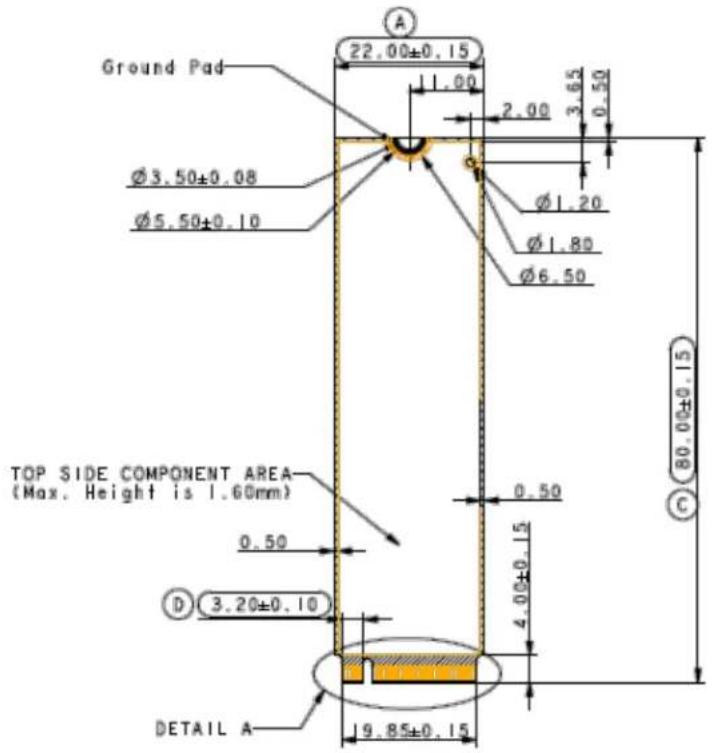
![18.50 0.50[PITCH] 0.35±0.04 C.L. E 0.55(Max.) (Gold Pad Leading Edge) 2.00±0.15 3.50±0.15 2.50 1.20±0.05 6.125 DETAIL A SCALE 2:1](/content/2026/05/1045769/images/b1e70003d095ea57be974978659d2c924ed4efc34749a78aa12d2352e07fa6e9.jpg)
Figure 2 Bottom View
![0.55 Ø1.20 Ø1.80 Ø6.00±0.10 Ground Pod 0.55 0.50 5.20[MIN.] Bottom Side Component Area (Max. Height is 1.60mm) DETAIL B](/content/2026/05/1045769/images/a41fcb90501f192cb8a562683a11f22188a075c2c75edc2d11577a3f1ce58b80.jpg)
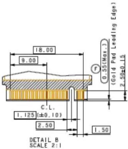
Figure 3 Side View
![1.60MAX 1.60MAX 4.00 [MIN] 5.20 [MIN] DETAIL C 0.80±0.08 G 20.0°±5.0° -2X 0.39±0.25-2X 0.58 (0.20 Min) DETAIL C SCALE 2:1](/content/2026/05/1045769/images/c6b9d696a2994a8f4160ee9c76ecb971ef1e9bd5053630fd4d2281013a7628fc.jpg)
4. Pin and Signal Descriptions
Table 11 Pin Descriptions
| Pin No PCIe Pin Description | ||
| 1 GND CONFIG_3=GND | ||
| 2 3.3V | 3.3V source | |
| 3 GND | Ground | |
| 4 3.3V | 3.3V source | |
| 5 PETn3 | PCIe TX Differential signal defined by the PCI Express M.2 spec | |
| 6 N/C | No connect | |
| 7 PETp3 | PCIe TX Differential signal defined by the PCI Express M.2 spec | |
| 8 N/C | No connect | |
| 9 GND | Ground | |
| 10 LED1# | Open drain, active low signal. These signals are used to allow the add- in card to provide status indicators via LED devices that will be provided by the system. | |
| 11 PERn3 | PCIe RX Differential signal defined by the PCI Express M.2 spec | |
| 12 3.3V | 3.3V source | |
| 13 PERp3 | PCIe RX Differential signal defined by the PCI Express M.2 spec | |
| 14 3.3V | 3.3V source | |
| 15 GND | Ground | |
| 16 3.3V | 3.3V source | |
| 17 | PETn2 | PCIe TX Differential signal defined by the PCI Express M.2 spec |
| 18 3.3V | 3.3V source | |
| 19 | PETp2 | PCIe TX Differential signal defined by the PCI Express M.2 spec |
| 20 | N/C | No connect |
| 21 GND | Ground | |
| 22 | N/C | No connect |
| 23 PERn2 | PCIe RX Differential signal defined by the PCI Express M.2 spec | |
| 24 | N/C | No connect |
| 25 PERp2 | PCIe RX Differential signal defined by the PCI Express M.2 spec | |
| 26 | N/C | No connect |
| 27 GND | Ground | |
| 28 | N/C | No connect |
| 29 | PETn1 | PCIe TX Differential signal defined by the PCI Express M.2 spec |
| 30 | N/C | No connect |
| 31 | PETp1 | PCIe TX Differential signal defined by the PCI Express M.2 spec |
| 32 | N/C | No connect |
| 33 GND | Ground | |
| 34 N/C | No connect | |
| 35 PERn1 | PCIe RX Differential signal defined by the PCI Express M.2 spec. | |
| 36 N/C | No connect | |
| 37 PERp1 | PCIe RX Differential signal defined by the PCI Express M.2 spec. | |
| 38 N/C | No connect | |
| 39 GND | Ground | |
| 40 | SMB_CLK(I/O)(0/1.8V) | SMBus Clock; Open Drain with pull-up on platform. |
| 41 PETn0 | PCIe TX Differential signal defined by the PCI Express M.2 spec. | |
| 42 | SMB_DATA(I/O)(0/1.8V) | SMBus Data; Open Drain with pull-up on platform. |
| 43 PETp0 | PCIe TX Differential signal defined by the PCI Express M.2 spec. | |
| 44 | ALERT#(O)(0/1.8V) | Alert notification to master; Open Drain with pull-up on platform; Active low. |
| 45 GND | Ground | |
| 46 N/C | No connect | |
| 47 PERn0 | PCIe RX Differential signal defined by the PCI Express M.2 spec. | |
| 48 N/C | No connect | |
| 49 PERp0 | PCIe RX Differential signal defined by the PCI Express M.2 spec. | |
| 50 | PERST#(I)(0/3.3V) | PE-Reset is a functional reset to the card as defined by the PCIe Mini CEM specification. |
| 51 GND | Ground | |
| 52 | CLKREQ#(I/O)(0/3.3V) | Clock Request is a reference clock request signal as defined by the PCIe Mini CEM specificati Also used by L1 PM Sub-states. |
| 53 REFCLKn | PCIe Reference Clock signals (100 MHz) defined by the PCI Express M.2 spec. | |
| 54 | PEWAKE#(I/O)(0/3.3V) | PCIe PME Wake.Open Drain with pull up on platform; Active Low. |
| 55 REFCLKp | PCIe Reference Clock signals (100 MHz) defined by the PCI Express M.2 spec. | |
| 56 | Reserved for MFG DATA | Manufacturing Data line. Used for SSD manufacturing only. Not used in normal operation.platform Socket. |
| 57 GND | Ground | |
| 58 | Reserved for MFG CLOCK | Manufacturing Clock line. Used for SSD manufacturing only.Not used in normal operation.Pins should be left N/C in platform Socket. |
| 59 | Module Key M | Module Key |
| 60 | Module Key M | |
| 61 | Module Key M | |
| 62 | Module Key M | |
| 63 | Module Key M | |
| 64 | Module Key M | |
| 65 | Module Key M | |
| 66 | Module Key M | |
| 67 N/C | No connect | |
| 68 | SUSCLK(32KHz) (I)(0/3.3V) | 32.768 kHz clock supply input that is provided by the platform chipset to reduce power and cost for the module. |
| 69 N/C | PEDET (NC-PCIe) | |
| 70 3.3V | 3.3V source | |
| 71 GND | Ground | |
| 72 3.3V | 3.3V source | |
| 73 GND | Ground | |
| 74 3.3V | 3.3V source | |
| 75 GNDZD | Ground | |
5. SMART Support
The Nytro 4350 SSD supports the SMART command set.
5.1 SMART IDs
The following table lists SMART IDs and Descriptions.
Table 12 SMART Attributes (Log Identifier 02h)
| Bytes Index Bytes Description | ||
| [0] 1 Critical Warning | ||
| [2:1] 2 Composite Temperature | ||
| [3] 1 Available Spare | ||
| [4] 1 Available Spare Threshold | ||
| [5] 1 Percentage Used | ||
| [31:6] 26 Reserved | ||
| [47:32] 16 Data Units Read | ||
| [63:48] 16 Data Units Written | ||
| [79:64] 16 Host Read Commands | ||
| [95:80] 16 Host Write Commands | ||
| [111:96] | 16 Controller Busy Time | |
| [127:112] | 16 Power Cycles | |
| [143:128] | 16 Power On Hours | |
| [159:144] | 16 Unsafe Shutdowns | |
| [175:160] | 16 Media and Data Integrity Errors | |
| [191:176] | 16 Number of Error Information Log Entries | |
| [195:192] | 4 Warning Composite Temperature Time | |
| [199:196] | 4 Critical Composite Temperature Time | |
| [201:200] | 2 Temperature Sensor 1 (Current Temperature) | |
| [203:202] | 2 Temperature Sensor 2 (N/A) | |
| [205:204] | 2 Temperature Sensor 3 (N/A) | |
| [207:206] | 2 Temperature Sensor 4 (N/A) | |
| [209:208] | 2 Temperature Sensor 5 (N/A) | |
| [211:210] | 2 Temperature Sensor 6 (N/A) | |
| [213:212] | 2 Temperature Sensor 7 (N/A) | |
| [215:214] | 2 Temperature Sensor 8 (N/A) | |
| [511:216] | 296 | Reserved |
NOTE (Optional) Contextual information for Log Identifier 02h:
■ Critical Warning [Byte 0]. This field indicates critical warnings for the state of the controller.
Bit#0: Available spare is below threshold
Bit#1: Temperature exceeded threshold or below an under temperature threshold
Bit#2: Reliability is degraded due to excessive media or internal errors
Bit#3: Media is placed in read only mode
BIt#4: Volatile memory backup device has failed
Bit#5 - Bit#7: Reserved
■ Available Spare [Byte 3]. This value (percentage) = 100* [(total reserved VB - consumed VB caused by early, later bad)/ total reserved VB]
■ Percentage Used [Byte 5]. This value (percentage) = 100* (total VB erase count/ PE cycle for total VB).
6. Feature Details
6.1 Flash Management
6.1.1 Error Correction Code (ECC)
Flash memory cells deteriorate with use. This can generate random bit errors in the stored data. The Nytro 4350 SSD applies the LDPC ECC algorithm to detect and correct errors occur during read process, to make sure the SSD reads correctly, and to protect data from corruption.
6.1.2 Wear Leveling
NAND flash devices can undergo only a limited number of program/erase cycles. Commonly, the SSD does not use areas of the flash media evenly. If the SSD updates some areas more frequently than others, this reduces the lifetime of the device. Wear Leveling extends the life of the NAND Flash by evenly distributing write and erase cycles across the media.
Seagate's advanced Wear Leveling algorithm spreads the flash usage throughout the whole flash media area. Implementing dynamic and static Wear Leveling algorithms improves the life expectancy of the NAND flash.
6.1.3 Bad Block Management
Bad blocks do not function properly and they can contain more invalid bits. This can make stored data unstable and bad block reliability is not guaranteed. Blocks identified and marked as bad by the manufacturer are called "Early Bad Blocks". Bad blocks that develop during the lifespan of the Flash are called "Later Bad Blocks". Seagate's bad block management algorithm detects the factory-produced bad blocks and manages bad blocks that appear with use. This practice prevents the drive from storing data in bad blocks and improves data reliability
6.1.4 TRIM
The TRIM feature improves the read/write performance and speed of SSDs. SSDs cannot overwrite existing data, so the available space becomes smaller with each data block use. The TRIM command runs within the operating system to tell the SSD which data blocks can be removed permanently because they are no longer in use. The SSD erases these unused data blocks.
6.1.5 SMART
SMART, stands for Self-Monitoring, Analysis, and Reporting Technology. SMART is an open standard that allows an SSD to automatically detect its health and report potential failures. When SMART records a failure, users can replace the SSD to prevent unexpected outage or data loss. SMART can also inform users of impending failures while there is still time to copy data to another device.
6.1.6 Over Provisioning
Over Provisioning (OP) preserves an additional area beyond user capacity in an SSD, which is not visible to users and cannot be used by them. OP improves performance and IOPS (Input/Output Operations per Second) by providing the controller additional space to manage P/E cycles. OP enhances the reliability and endurance as well. Moreover, the write amplification of the SSD becomes lower when the controller writes data to the flash.
6.1.7 Firmware Upgrade
Firmware provides a set of instructions on how the device communicates with the host. Firmware upgrades are typically available with added features, fixed compatibility issues, and improved read/write performance.
6.1.8 Thermal Throttling
Thermal throttling prevents components in an SSD from over-heating during read and write operations. The Nytro 4350 SSD design provides an on-die and on-board thermal sensor. With this accuracy, firmware can apply different levels of throttling to protect efficiently and proactively through the SMART reading.
Table 13 Current version: Thermal Throttling 2.0
| Item Content | |
| Smart reporting temperature Flash normalized case temperature | |
| Reference of temp. reading On-board thermal sensor, | Controller on-die thermal sensor |
| tmt1 threshold | 76°C per Smart reported |
| tmt2 threshold | 79°C per Smart reported |
| Protect controller threshold | 115°C from on-die thermal sensor |
| Fatal threshold | 120°C from on-die thermal sensor |
| Resume performance threshold | 72°C per Smart reported |
| Temperature polling frequency Every 1 sec | |
| TMT1_state impact ±10% CE | |
| TMT2_state impact -20% CE | |
6.1.9 Multiple Namespaces
An NVMe namespace is a quantity of non-volatile memory (NVM) that can be formatted into logical blocks.
Namespaces are used when a storage virtual machine is configured with the NVMe protocol. Nytro 4350 SSD supports up to 16 namespaces for greater deployment flexibility.
6.1.10 Garbage Collection
Garbage collection allocates and releases memory to accelerate the read/write processing and improve performance. When there is less available space, the SSD slows down the read/write processing and implements garbage collection to release memory.
6.2 Advanced Device Security Features
6.2.1 Secure Erase
Secure Erase is a standard NVMe format command and it writes all of "0x00" to fully wipe all the data on hard drives and SSDs. When this command issues, the SSD controller erases its storage blocks and returns to its factory default settings.
6.2.2 Physical Presence SID
TCG defines Physical Presence SID (PSID) as a 32-character string. PSID reverses the SSD to its manufacturing setting when the SSD is set through TCG Pyrite (non-SED). The PSID code is printed on the SSD label. PSID erases all data when reverting the SSD to manufacturing settings.
6.2.3 Sanitize
The Sanitize feature uses the Format NVM command to provide an alternative to the existing secure erase capabilities. This feature provides robust data security by making sure the user data from the SSD media, caches, and the Controller Memory Buffer are erased by the block erase operations, overwriting or destroying the encryption key. The following table shows the types of Sanitize Operations supported.
Table 14 Sanitize Operations
| SSD Security Type | Sanitize Operation TCG Commands | ||||
| Overwrite Block Erase | Crypto Erase | PSID Revert Process | Instant Security Erase | ||
| Non-SED (TCG Pyrite) Yes Yes No Yes | No | ||||
NOTE Sanitize Overwrite command erases all data on the disk beyond all feasible effort to recover. Completion takes at least one hour per terabyte per pass. The number of passes is drive-selectable. The NVMe spec default is 16 passes. Contact Seagate Support for more detailed information.
6.3 SSD Lifetime Management
Drive Writes per Day (DWPD) The Total Bytes Written (TBW) specification of an SSD calculates how many times you can write the user capacity of an SSD per day over the warranty period (or a different number of years), based on the JEDEC workload used to specify the TBW.
$$ D W P D = (T B W \text { of an SSD x 1024) / (Warranty days x SSD size in GB) } $$
TBW measures the lifespan of the SSD. This measurement represents the amount of data written to the device. To calculate the TBW of an SSD, use the following equation:
$$ \mathrm{TBW} = \left[ (\text { N A N D E n d u r a n c e }) \times (\text { S S D C a p a c i t y }) \right] / [ \text { W A F } ] $$
NAND Endurance: NAND endurance refers to the P/E (Program/Erase) cycle of a NAND flash.
SSD Capacity: The SSD capacity is the specific capacity in total of an SSD.
WAF: Write Amplification Factor (WAF) is a numerical value. This value represents the ratio between the amount of data that an SSD controller needs to write and the amount of data that the host's flash controller writes. A WAF, near 1, guarantees better endurance and lower frequency of data written to flash memory.
TBW in this document is based on the JEDEC 218/219 workload.
6.3.1 Media Wear Indicator
The SMART attribute byte index [5], Percentage Used, reports the Actual Life Indicator. Replace the SSD when this number reaches 100%.
6.3.2 Read Only Mode (End of Life)
When program/erase cycles age the SSD, media wear-out can cause increasing numbers of bad blocks. When the number of usable good blocks is less than the threshold (5%, SMART attribute log ID 02h Byte4), the SSD notifies the host through an AER event and Critical Warning to enter Read Only Mode to prevent further data corruption. When this happens, replace the SSD immediately.
6.4 Adaptive Approach to Performance Tuning
6.4.1 Predict and Fetch
When the Host tries to read data from the SSD, the SSD performs only one read action after receiving one command. However, the Nytro 4350 SSD applies Predict and Fetch to improve the read speed. When the host issues sequential read commands to the SSD, the SSD expects that the following are also read commands. Therefore, before receiving the next command, flash has prepared the data. This accelerates data processing time, and the host needs less wait time to receive data.
6.4.2 Throughput
Based on the available space of the SSD, the Nytro 4350 SSD regulates the read/write speed and manages the performance of throughput. When the SSD has more space, the firmware continuously performs read/write actions. When the SSD has less available space, it slows down the read/write processing and implements garbage collection to release memory.
7. Safety Certifications, and Compliance
You can find up to date information on safety certifications, and component compliance requirements for Seagate devices on the Seagate Support page, here: https://www.seagate.com/support/
For a direct link to the Seagate HDD and SSD Regulatory Compliance and Safety document, go here: https://www.seagate.com/files/www-content/forms/compliance/regulatory-compliance-and-safety-100838899-A.pdf
7.1 Regulatory Model Numbers
The following regulatory model number represents all Seagate Nytro 4350 SSD:
STA039
8. Installation Precautions
8.1 Handling Precautions
There are a lot of components assembled on a single SSD device. Please handle the drive with careespecially when it has any WLCSP (Wafer Level Chip Scale Packaging) components such as PMIC, thermal sensor or load switch. WLCSP is one of the packaging technologies that is widely adopted for making smaller footprints, but any bumps or scratches may damage those ultrasmall parts so gentle handling is strongly recommended.

DO NOT DROP SSD
INSTALL SSD WITH CARE
STORE SSD IN A PROPER PACKAGE
8.2 Assembly Precautions
M Key M.2 SSD (Figure 1) is only compatible to M Key (Figure 2) socket. As shown in Use Case 2, misuse may cause severe damages to SSD including burn-out.
natural_image
Diagram of a battery pack with a right-pointing arrow indicating direction (no text or symbols)Use Case 1. M-key notch needs to be attached to M-key edge of M.2 SSD.
Figure 2. M Key Socket
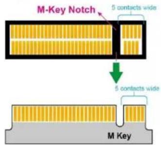
Figure 1. M Key M.2 SSD
Use Case 2. B-key notch will not fit to M-key edge of M.2 SSD.
Figure 3. B Key Socket
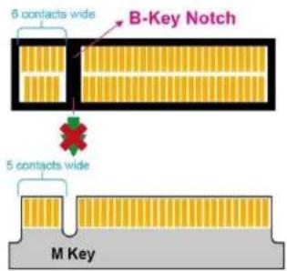
Figure 1. M Key M.2 SSD

SEAGATE
Seagate Technology LLC
AMERICAS Seagate Technology LLC 47488 Kato Road, Fremont, California 94538, United States, 510-661-1000
ASIA/PACIFIC Seagate Singapore International Headquarters Pte. Ltd. 7000 Ang Mo Kio Avenue 5, Singapore 569877, 65-6485-3888
EUROPE, MIDDLE EAST AND AFRICA Seagate Technology Netherlands BV, Tupolevlaan, 105, 119 PA Schipol-Rijk. the Netherlands
Publication Number: 205237900, Rev B
December 2023