
MAC-SA5X-KIT - Horloge atomique Microchip - Free user manual and instructions
Find the device manual for free MAC-SA5X-KIT Microchip in PDF.


| Product Type | Development Kit |
| Brand | Microchip |
| Model | MAC-SA5X-KIT |
| Dimensions | Approx. 100 x 60 x 15 mm |
| Weight | Approx. 50 g |
| Power Supply | 5V via USB or external 7-12V DC |
| Microcontroller | ARM Cortex-M based MCU (SAM series) |
| GPIO Pins | 20+ digital I/O, analog inputs |
| Interfaces | USB, UART, I2C, SPI, PWM |
| Memory | 256KB Flash, 64KB SRAM |
| Clock Speed | Up to 120 MHz |
| Integrated Debugger | On-board programmer/debugger (mEDBG or similar) |
| Operating Temperature | -40°C to +85°C |
| Software Support | MPLAB X IDE, Arduino IDE (via third-party) |
| Main Functions | Prototyping, evaluation, and development of embedded systems |
| Maintenance | Keep dry; clean with soft cloth; avoid static discharge |
| Safety | Use ESD protection; do not exceed voltage ratings |
| Spare Parts | Not applicable; replace entire kit if damaged |
| Repairability | Not user-serviceable; for repair contact Microchip support |
| General Information | Designed for rapid prototyping with Microchip SAM series microcontrollers |
Frequently Asked Questions - MAC-SA5X-KIT Microchip
User questions about MAC-SA5X-KIT Microchip
0 question about this device. Answer the ones you know or ask your own.
Ask a new question about this device
Download the instructions for your Horloge atomique in PDF format for free! Find your manual MAC-SA5X-KIT - Microchip and take your electronic device back in hand. On this page are published all the documents necessary for the use of your device. MAC-SA5X-KIT by Microchip.
USER MANUAL MAC-SA5X-KIT Microchip
Note the following details of the code protection feature on Microchip products:
• Microchip products meet the specifications contained in their particular Microchip Data Sheet.
- Microchip believes that its family of products is secure when used in the intended manner, within operating specifications, and under normal conditions.
- Microchip values and aggressively protects its intellectual property rights. Attempts to breach the code protection features of Microchip product is strictly prohibited and may violate the Digital Millennium Copyright Act.
- Neither Microchip nor any other semiconductor manufacturer can guarantee the security of its code. Code protection does not mean that we are guaranteeing the product is "unbreakable" Code protection is constantly evolving. Microchip is committed to continuously improving the code protection features of our products.
This publication and the information herein may be used only with Microchip products, including to design, test, and integrate Microchip products with your application. Use of this information in any other manner violates these terms. Information regarding device applications is provided only for your convenience and may be superseded by updates. It is your responsibility to ensure that your application meets with your specifications. Contact your local Microchip sales office for additional support or, obtain additional support at https://www.microchip.com/en-us/support/design-help/client-support-services.
THIS INFORMATION IS PROVIDED BY MICROCHIP "AS IS". MICROCHIP MAKES NO REPRESENTATIONS OR WARRANTIES OF ANY KIND WHETHER EXPRESS OR IMPLIED, WRITTEN OR ORAL, STATUTORY OR OTHERWISE, RELATED TO THE INFORMATION INCLUDING BUT NOT LIMITED TO ANY IMPLIED WARRANTIES OF NON-INFRINGEMENT, MERCHANTABILITY, AND FITNESS FOR A PARTICULAR PURPOSE, OR WARRANTIES RELATED TO ITS CONDITION, QUALITY, OR PERFORMANCE.
IN NO EVENT WILL MICROCHIP BE LIABLE FOR ANY INDIRECT, SPECIAL, PUNITIVE, INCIDENTAL, OR CONSEQUENTIAL LOSS, DAMAGE, COST, OR EXPENSE OF ANY KIND WHATSOEVER RELATED TO THE INFORMATION OR ITS USE, HOWEVER CAUSED, EVEN IF MICROCHIP HAS BEEN ADVISED OF THE POSSIBILITY OR THE DAMAGES ARE FORESEEABLE. TO THE FULLEST EXTENT ALLOWED BY LAW, MICROCHIP'S TOTAL LIABILITY ON ALL CLAIMS IN ANY WAY RELATED TO THE INFORMATION OR ITS USE WILL NOT EXCEED THE AMOUNT OF FEES, IF ANY, THAT YOU HAVE PAID DIRECTLY TO MICROCHIP FOR THE INFORMATION.
Use of Microchip devices in life support and/or safety applications is entirely at the buyer's risk, and the buyer agrees to defend, indemnify and hold harmless Microchip from any and all damages, claims, suits, or expenses resulting from such use. No licenses are conveyed, implicitly or otherwise, under any Microchip intellectual property rights unless otherwise stated.
For information regarding Microchip's Quality Management Systems, please visit www.microchip.com/quality.
Trademarks
The Microchip name and logo, the Microchip logo, Adaptec, AVR, AVR logo, AVR Freaks, BesTime, BitCloud, CryptoMemory, CryptoRF, dsPIC, flexPWR, HELDO, IGLOO, JukeBlox, KeeLoq, Kleer, LANCheck, LinkMD, maXStylus, maXTouch, MediaLB, megaAVR, Microsemi, Microsemi logo, MOST, MOST logo, MPLAB, OptoLyzer, PIC, picoPower, PICSTART, PIC32 logo, PolarFire, Prochip Designer, QTouch, SAM-BA, SenGenuity, SpyNIC, SST, SST Logo, SuperFlash, Symmetricom, SyncServer, Tachyon, TimeSource, tinyAVR, UNI/O, Vectron, and XMEGA are registered trademarks of Microchip Technology Incorporated in the U.S.A. and other countries.
AgileSwitch, APT, ClockWorks, The Embedded Control Solutions Company, EtherSynch, Flashtec, Hyper Speed Control, HyperLight Load, Libero, motorBench, mTouch, Powermite 3, Precision Edge, ProASIC, ProASIC Plus, ProASIC Plus logo, Quiet-Wire, SmartFusion, SyncWorld, Temux, TimeCesium, TimeHub, TimePictra, TimeProvider, TrueTime, and ZL are registered trademarks of Microchip Technology Incorporated in the U.S.A.
Adjacent Key Suppression, AKS, Analog-for-the-Digital Age, Any Capacitor, AnyIn, AnyOut, Augmented Switching, BlueSky, BodyCom, Clockstudio, CodeGuard, CryptoAuthentication, CryptoAutomotive, CryptoCompanion, CryptoController, dsPICDEM, dsPICDEM.net, Dynamic Average Matching, DAM, ECAN, Espresso T1S, EtherGREEN, GridTime, IdealBridge, In-Circuit Serial Programming, ICSP, INICnet, Intelligent Paralleling, IntelliMOS, Inter-Chip Connectivity, JitterBlocker, Knob-on-Display, KoD, maxCrypto, maxView, memBrain, Mindi, MiWi, MPASM, MPF, MPLAB Certified logo, MPLIB, MPLINK, MultiTRAK, NetDetach, Omniscient Code Generation, PICDEM, PICDEM.net, PICkit, PICtail, PowerSmart, PureSilicon, QMatrix, REAL ICE, Ripple Blocker, RTAX, RTG4, SAM-ICE, Serial Quad I/O, simpleMAP, SimpliPHY, SmartBuffer, SmartHLS, SMART-I.S., storClad, SQI, SuperSwitcher, SuperSwitcher II, Switchtec, SynchroPHY, Total Endurance, Trusted Time, TSHARC, USBCheck, VariSense, VectorBlox, VeriPHY, ViewSpan, WiperLock, XpressConnect, and ZENA are trademarks of Microchip Technology Incorporated in the U.S.A. and other countries.
SQTP is a service mark of Microchip Technology Incorporated in the U.S.A.
The Adaptec logo, Frequency on Demand, Silicon Storage Technology, and Symmcom are registered trademarks of Microchip Technology Inc. in other countries.
GestIC is a registered trademark of Microchip Technology Germany II GmbH & Co. KG, a subsidiary of Microchip Technology Inc., in other countries.
All other trademarks mentioned herein are property of their respective companies.
© 2019 - 2024, Microchip Technology Incorporated and its subsidiaries.
All Rights Reserved.
ISBN: 978-1-6683-4328-9
Preface
NOTICE TO CUSTOMERS
All documentation becomes dated, and this manual is no exception. Microchip tools and documentation are constantly evolving to meet customer needs, so some actual dialogs and/or tool descriptions may differ from those in this document. Please refer to our website (www.microchip.com) to obtain the latest documentation available.
Documents are identified with a "DS" number. This number is located on the bottom of each page, in front of the page number. The numbering convention for the DS number is "DSXXXXXXXXA", where "XXXXXXXXX" is the document number and "A" is the revision level of the document.
For the most up-to-date information on development tools, see the MPLAB ® IDE online help. Select the Help menu, and then Topics, to open a list of available online help files.
PURPOSE OF THIS GUIDE
The MAC-SA5X User's Guide provides basic recommendations for designing products to use Microchip's Miniature Atomic Clock (MAC) SA5X. The guidelines in the document are generic because specific product requirements vary between applications.
This material consists of a brief description of SA5X design supported by block diagrams, description of environmental issues, installation guidelines, and unit operation.
WHO SHOULD READ THIS GUIDE
This document is intended for engineers and telecommunications professionals who are designing, installing, operating, or maintaining time, frequency, and synchronization systems that require a low profile and highly precise frequency generator.
To use this document effectively, you must have a good understanding of digital telecommunications technologies, analog frequency generation, and synthesis techniques.
DOCUMENT LAYOUT
This guide contains the following sections and appendixes:
- Chapter 1. "Product Overview": Provides an overview of the product, describes the major hardware and software features, and lists the system specifications.
- Chapter 2. "Installation": Contains procedures for unpacking and installing the system, and for powering up the unit.
- Chapter 3. "Operation": Describes procedures for frequency adjustment and toggling on/off various features.
- Chapter 4. "Command Line Interface": Describes the CLI command conventions, functions, and features.
- Chapter 5. "Maintenance and Troubleshooting": Contains maintenance and troubleshooting procedures for the product. Also contains procedures for returning the MAC.
- Appendix A. "Principle of Operation": Briefly explains Atomic Interrogation and
Coherent Population Trapping
- Appendix B. "Legacy Command Set (SA.3Xm)": Describes the Legacy CLI command conventions, functions, and features. For backwards compatibility.
- Appendix C. "Reference Designs": Provides generic sample schematics for converting MAC input/output signals.
- Appendix D. "Evaluation Kit": Describes the evaluation kit for use with the MAC.
- Appendix E. “Software License Agreements”: Describes the open source software that portions of the SA5X software makes use of.
CONVENTIONS USED IN THIS GUIDE
This manual uses the following documentation conventions:
- Acronyms and Abbreviations: Terms are spelled out the first time they appear in text. Thereafter, only the acronym or abbreviation is used. This guide uses "SA5X" and "MAC" interchangeably. SA5X is the latest generation of Miniature Atomic Clock (MAC).
- Unless explicitly labeled with Hz, MHz, etc, all references to “frequency offset” throughout this document imply the industry-standard fractional frequency Δf/f , where “ Δf ” is the difference between nominal and measured value (in Hz), and “f” is the nominal frequency (in Hz).
WARNINGS, CAUTIONS, RECOMMENDATIONS, AND NOTES
Warnings, Cautions, Recommendations, and Notes attract attention to essential or critical information in this guide. The types of information included in each are displayed in a style consistent with the examples below.
WARNING
To avoid serious personal injury or death, do not disregard warnings. All warnings use this style. Warnings are installation, operation, or maintenance procedures, practices, or statements that, if not strictly observed, may result in serious personal injury or even death.
CAUTION
To avoid personal injury, do not disregard cautions. All cautions use this style. Cautions are installation, operation, or maintenance procedures, practices, or statements that, if not strictly observed, may result in damage to, or destruction of, the equipment. Cautions are also used to indicate long-term health hazards.
Note: All notes use this style. Notes contain installation, operation, or maintenance procedures, practices, conditions, or statements that alert you to important information that may make your task easier or increase your understanding.
WHERE TO FIND ANSWERS TO PRODUCT AND DOCUMENT QUESTIONS
For additional information about the products described in this guide, please contact your Microchip representative or your local sales office. You can also contact us on the web at: https://microchip.my.site.com/s/
When this manual is updated the latest version will be available for downloading from Microchip's web site. Manuals are provided in PDF format for ease of use. After downloading, you can view the manual on a computer or print it using Adobe Acrobat Reader.
Manual updates are available at: https://www.microchip.com
RELATED DOCUMENTS AND INFORMATION
See your Microchip representative or sales office for a complete list of available documentation. To order any accessory, contact the Microchip Sales Department. If you encounter any difficulties installing or using the product, contact Microchip Frequency and Time Systems (FTS) Services and Support:
North and South America
Microchip FTS
3870 North First Street
San Jose, CA 95134-1702
Toll-free in North America: +1 888-367-7966, Option 1
Telephone: +1 408-428-7907
Email: sjo-ftd.support@microchip.com
Europe, Middle East, and Africa (EMEA)
Microchip FTS
Altlaufstrasse 42
Level 15.01, 1 First Avenue, 2A Dataran Bandar Utama
Damansara, 47800 Petaling Jaya
Selangor, Malaysia
Toll-free in North America: 1-888-367-7966, Option 1
Telephone: +1 408-428-7907
Email: sjo-ftd.support@microchip.com
THE MICROCHIP WEBSITE
Microchip provides online support via our website at www.microchip.com. This website is used as a means to make files and information easily available to customers.
Accessible by using your favorite Internet browser, the website contains the following information:
- Product Support – Data sheets and errata, application notes and sample programs, design resources, user's guides and hardware support documents, latest software releases and archived software
- General Technical Support – Frequently Asked Questions (FAQs), technical support requests, online discussion groups, Microchip consultant program member listing
- Business of Microchip – Product selector and ordering guides, latest Microchip press releases, listing of seminars and events, listings of Microchip sales offices, distributors and factory representatives
CUSTOMER SUPPORT
Users of Microchip products can receive assistance through several channels:
- Distributor or Representative
- Local Sales Office
• Field Application Engineer (FAE) - Technical Support
Customers should contact their distributor, representative or field application engineer (FAE) for support. Local sales offices are also available to help customers. A listing of sales offices and locations is included in the back of this document.
Technical support is available through the website at:
http://www.microchip.com/support.
DOCUMENT REVISION HISTORY
Revision A (November 2019)
- Initial release of this document as Microchip DS50002938A.
- Under Microsemi's literature system, this document is number 900-44500-000, Rev. A.
Revision B (March 2021)
- Updated mechanical drawings and images (Figure 1-1, Figure 1-2, Figure 2-1, Figure 2-3) to accurately reflect the labeling as it is manufactured. Top labels have been rotated 90 degrees. Previous drawings did not show proper label orientation.
Revision C (December 2022)
- Added information about the DisciplineTuning parameter and Sync command to the following sections: Section 3.3, Section 3.3.1, Section 3.4.1, Section 3.4.3, Section 4.5.2, Table 4-6, and Table 4-12.
Revision D (July 2023)
- Added information about the id? command with changes to Section 3.4.2, Section 3.5; Section 4.5.2, Table 4-6; and Table 4-12.
- Other minor text changes made where needed.
Revision E (April 2024)
- Added information about the pn? command with changes to Section 4.5.2 and Table 4-12.
Table of Contents
Preface 3
Purpose of This Guide.... 3
Who Should Read This Guide.... 3
Document Layout 3
Conventions Used in this Guide 4
Warnings, Cautions, Recommendations, and Notes...... 4
Where to Find Answers to Product and Document Questions 5
Related Documents and Information.... 5
The Microchip Website....5
Customer Support 6
Document Revision History 6
Chapter 1. Product Overview
1.1 MAC-SA5X Overview 9
1.1.1 Key Features 10
1.2 Physical Description 10
1.2.1 Communications Connections.... 11
1.2.2 Input Connections 11
1.2.3 Output Connections.... 11
1.2.4 Power and Ground Connections 12
1.3 Functional Description.... 12
1.4 Configuration Management 13
1.5 Alarms 13
Chapter 2. Installation
2.1 Handling Considerations 15
2.2 Mounting Considerations .... 15
2.21 Absolute Minimum and Maximum Ratings 19
2.3 Start-Up Sequence 19
Chapter 3. Operation
3.1 Configure the Serial Port 21
3.2 Analog Tuning 21
3.3 Digital Tuning 22
3.3.1 Calibration 22
3.4 1PPS Disciplining 23
3.4.1 Theory 23
3.4.2 Selection of Disciplining Time Constant, "Tau" 25
3.4.6 PPS Quantization Error Correction 27
3.5 Device Information and Status 27
3.6 Time of Day (TOD).... 27
Chapter 4. Command Line Interface
4.1 Command Structure 29
4.1.1 Sequence Number ....30
4.1.2 Arguments....30
4.1.3 Command Checksum .... 30
4.2 Response Structure.... 30
4.2.1 Error Response....31
4.2.2 Response Checksum....32
4.3 Announcement Structure.... 32
4.4 Parameters.... 32
4.4.1 Parameter Index ......33
4.4.2 Parameter Attributes ....34
4.4.2.1 Parameter Units Attribute....35
4.4.3 Alarms Parameter ....36
4.5 Commands.... 38
4.5.1 Command Index....38
4.5.2 Command Usage ....39
Chapter 5. Maintenance and Troubleshooting
5.1 Preventative Maintenance.... 45
5.2 Electrostatic Discharge (ESD) Considerations.... 45
5.3 Troubleshooting.... 45
5.4 Repairing the MAC.... 45
5.5 Upgrading the Firmware.... 45
5.6 Returning the MAC.... 45
Appendix A. Principle of Operation....47
Appendix B. Legacy Command Set (SA.3Xm)
B.1 Legacy Command Structure 49
B.2 Legacy Command Index.... 50
B.3 Legacy Command Usage 50
Appendix C. Reference Designs ....53
Appendix D. Evaluation Kit
D.1 Overview and Key Features 57
D.2 Physical Description 58
D.2.1 Communications Connections....59
D.2.2 Input Connections ....60
D.2.3 Output Connections....60
D.2.4 Power Connections ....60
D.2.5 Functional Description and Operation 60
D.2.5.1 Troubleshooting....61
Appendix E. Software License Agreements 63
Worldwide Sales and Service 65
Chapter 1. Product Overview
1.1 MAC-SA5X OVERVIEW
The MAC is a source of stable output frequency. Because it relies on the Atomic resonance of Rubidium Isotope 87 (87Rb) gas to generate the RF output, it is less susceptible to instabilities produced from the mechanical and thermal stresses inherent in Quartz oscillators, enabling superior mid- to long-term accuracy. This stability makes it suitable as a holdover reference in GPS denied environments. Frequency errors can be corrected by applying a digital command or external correction voltage to the MAC. (See Frequency steering and Section 3.2 “Analog Tuning”). Frequency drift (Aging rate) can also be corrected by implementing the 1PPS disciplining feature of the MAC. When combined with a GNSS receiver, this feature allows the system designer to combine the short-term stability of a Rb reference with the long-term stability of the GNSS, approaching the performance of laboratory-grade Cesium Beam Tube frequency standards (see Section 3.4 “1PPS Disciplining”).
The Miniature Atomic Clock (MAC) SA5X is Microchip's seventh generation gas cell atomic oscillator technology product. It was designed to accommodate a variety of timing applications as well as to replace several legacy Rubidium products (SA.22c, x72 and MAC-SA.3Xm). The footprint is compatible with the SA.3Xm, but with several advancements in technology and features. Users of the previous generation (SA.3Xm) can now expect improvements to frequency stability, warm-up time, input voltage range, and operational temperature range. Additionally, 1 PPS disciplining and USB connections via a new embedded Molex™ connector allow greater design capabilities. The 1 PPS input allows users to quickly calibrate frequency and phase of the MAC to a primary clock such as GPS, while the RF and 1 PPS outputs provide highly stable holdover references.

FIGURE 1-1: The Miniature Atomic Clock (MAC) SA5X.
The MAC reflects significant advances in physics miniaturization and atomic interrogation algorithms that serve to reduce size and power while providing a stable reference frequency that is resistant to environmental perturbation. The SA5X comes in several performance levels to meet a range of system requirements. The SA5X offers a low height (18.3 mm/0.72 in), a small footprint (50.8 mm × 50.8 mm, or 2 in × 2 in), and an industrial operating temperature range of -40°C to +75°C (measured at the baseplate). It is refined for cost effective mass production and can be easily integrated into time, frequency, and synchronization systems. The SA5X requires a single supply voltage and can be mounted directly onto a circuit board as a component of a module used in 20 mm (0.8 in) wide card slots. The design produces a stable frequency with good short and long term stability, and excellent phase noise performance.
This user guide provides engineering information for use of the SA5X. It also provides supporting information for use of the Evaluation Kit (p/n 090-44500-000). Furthermore, the design details of the Evaluation Kit can be used to assist with host system design (for example, power conditioning, signal buffering, and so on). This user guide must be used in conjunction with the current data sheet for the SA5X, which is available on the Microchip web site.
1.1.1 Key Features
• 10 MHz CMOS Output
- 1PPS Disciplining
• 1PPS LVDS Inputs and Output
- -40°C to +75°C Operating Temperature (Baseplate)
- -55°C to +100°C Storage Temperature
- USB 2.0-Compatible Communication Pins
- Wide Range Allowable DC Input (4.5 to 32V)
- Fast Warm-Up Time (<7 Minutes from -10°C to +75°C )
- < 5 × 10-11 Monthly Aging Rate (On for 30 Days Prior)
- <100 ns Time Error in 24 hrs (Calculated Based on 5 × 10-11 / mo . Aging Rate, Assuming Zero Initial Phase/Frequency Offset, Static Environment, On for 30 Days Prior to Holdover)
- Serial/USB Interface for Digital Steering, Configuration, and Diagnostics
1.2 PHYSICAL DESCRIPTION
Labels will contain information about the part number and the serial number. The serial number indicates the initial time of manufacture in the following manner. The first two digits of serial number indicate the year of manufacture (18 = 2018). Digits three and four indicate the month of manufacture (01 = January).
The MAC consists of a 2 in x 2 in x 0.7 in PCB-mountable chassis, consisting of a Nickel-plated Aluminum baseplate and black anodized Aluminum cover. All connections for the MAC are on the baseplate. Figure 1-2 shows the top cover on the left and the bottom baseplate on the right.
See Figure 2-1 for a complete mechanical drawing.
![PIN 1 PIN 2 PIN 3 [±0.025] 8X Ø.040±.001 [6,7] 8X .27 PIN 8 PIN 7 PIN 6 PIN 4 J1 CONNECTOR (20 PIN MOLEX PN 53748-0208) MINIWAHA ME - MOLEXEN J200VAH [18,2]*0,5 -0,3 .715*0,020 .010](/content/2026/05/958759/images/278a527f3cccc6d7cec2f7415953dc47e93f5e8accd698d28f867feef82224cf.jpg)
![MICROCHIP MAC PART NO. 000000 Methanum Automatic Qucts. US Presses 62703 & 62802 [50.8] 2.00 [50.8] 2.00](/content/2026/05/958759/images/94726203fd7f16d63c09ee9a7b8066a04591db81fa55243ee618505b0698b87a.jpg)
FIGURE 1-2: Top Cover and Bottom Baseplate.
The baseplate consists of eight backwards-compatible gold-plated pins and recessed 20-lead Molex ™ connector for new features (1PPS, USB, etc).
| J1 CONNECTOR PINOUTS | |||
| PIN NO. | FUNCTION | PIN NO. | FUNCTION |
| 1 | PPS-IN 1+ | 2 | USB DATA + |
| 3 | PPS-IN 1- | 4 | USB DATA - |
| 5 | PPS-IN 0+ | 6 | USB POWER |
| 7 | PPS-IN 0- | 8 | GND |
| 9 | GND | 10 | NC |
| 11 | NC | 12 | NC |
| 13 | NC | 14 | NC |
| 15 | GND | 16 | NC |
| 17 | PPS-OUT + | 18 | NC |
| 19 | PPS-OUT - | 20 | ALARM |
NC - PINS THAT SHOULD HAVE NO CONNECTION. RESERVED FOR FACTORY OR FUTURE FUNCTIONS.

SCALE 4:1 MATING CONNECTOR MOLEX PN 52991-0208
| PIN NO. | FUNCTION |
| 1 | INPUT FREQUENCY CONTROL |
| 2 | CASE GROUND |
| 3 | RF OUTPUT |
| 4 | GND (SUPPLY & SIGNAL) |
| 5 | INPUT SUPPLY (+4.5 TO +32 VDC) |
| 6 | BITE |
| 7 | RS-232 TX |
| 8 | RS-232 RX |
FIGURE 1-3: Pinout.
1.2.1 Communications Connections
The MAC is controlled either by the legacy serial port pins or with the high speed USB-compatible pins on the Molex connector.
- Serial Console Port: The serial port connection is made through pins 7 and 8 on the baseplate of the MAC. This port allows a user to connect to a terminal or computer using a terminal emulation software package. When connecting to this port, use an appropriate converter chip such as the TRS3122E or similar to attain the required LVCMOS levels. Figure 1-2 shows the serial port pins 7 and 8 in the lower-right region of the baseplate. The default speed is 57600 bps and higher speeds of 230400 bps and 921600 bps are available.
- USB Port: The USB port is capable of making high speed communication with the MAC though the Molex (J1) connector pins J-2, 4, and 6.
Note: "Compatibility" commands are not supported when communicating via USB port. See Appendix B. "Legacy Command Set (SA.3Xm)".
1.2.2 Input Connections
- Analog Tuning: Analog Tuning is available on pin 1 for steering the MAC output frequency by means of an externally supplied DC voltage. This method is for legacy applications that cannot steer the MAC digitally via the serial/USB interface.
- 1PPS Input (x2): Two selectable LVDS 1PPS inputs can be provided on pins J1-5,7 (PPS0-IN) or J1-1,3 (PPS1-IN) for aligning the MAC's frequency and timing output with an externally applied 1PPS reference signal. The PPS input is selected via digital interface. Default input is PPS0-IN.
1.2.3 Output Connections
• 10 MHz RF Output: One CMOS output is available on pin 3.
- 1PPS Output: A single differential LVDS 1PPS output is available on pins J1-17, 19.
- Built-In Test Equipment (BITE): An active-low CMOS output on pin 6 signifies that the MAC has achieved atomic lock.
- Alarm Output: An active-low CMOS output on pin J1-20 indicates if an alarm condition is present. The user can read the Alarm bits through the USB/Serial interface to determine which alarm was triggered.
1.2.4 Power and Ground Connections
The MAC is not equipped with a power switch. DC power is applied on pin 5 with ground pins located on pins 2 and 4. If the J1 connector is used, pins J1-8, J1-9, and J1-15 should be grounded. Remaining pins should remain as "No Connect" (NC) unless indicated otherwise in Figure 1-3. If J1 connector is unused, all pins should remain as "No Connect".
Recommendation: It is recommended to tie ground (Pin 4) to same node as the baseplate ground Pin 2.
1.3 FUNCTIONAL DESCRIPTION
Communication Ports
These ports can be used to configure the MAC with Microchip's C3 software commands using a terminal or a computer with terminal emulation software. The default settings for the serial port are:
- Baud = 57.6K
- Data Bits = 8 bits
- Parity = None
- Stop bits = 1
- Flow Control = None
Commands allow the user to:
- Turn Analog tuning on or off
• Digitally adjust the output frequency - Configure 1PPS Disciplining settings
- Query the MAC's health/lock/alarm status
- Configure the Time of Day
Analog Tuning Input
Analog tuning is a means of steering the MAC's output frequency by applying a DC tuning voltage to Pin 1. This is useful for legacy applications where digital frequency steering is not possible.
1PPS Inputs
The MAC offers two selectable 1PPS inputs for use in steering the output RF (and 1PPS Output, simultaneously). PPS_Input_0 (pins J1-5,7) and PPS_Input_1 (pin J1-1,3) are selectable with the PpsSource parameter. Their 1PPS Disciplining settings can be adjusted independently, however, the MAC can only discipline to one input at a time. If a valid PPS signal on the selected input is present, then the parameter PpsInDetected = 1. See Section 3.4 "1PPS Disciplining" for more details.
CAUTION
An LVDS square wave 1PPS is the allowable input.
10 MHz Output
The 10 MHz RF output appears on Pin 3 as soon as the MAC is switched ON and is always present, regardless of the lock status. When the MAC is out of lock (Locked = 0/Logic-High BITE pin), the output frequency is provided by the free-running TCXO, which has frequency accuracy specification of ±2 ppm over its operating range. The output format is 3.3V LVCMOS compatible.
Note: If a high-level (high-power) output driver is required, a driver circuit must be implemented external to the MAC.
1PPS Output
An LVDS 1 pulse-per-second (1PPS) square wave output is available on pins J1-17,19 upon power-up. The 1PPS output is derived by digital division of the RF reference frequency and cannot be de-coupled. Therefore, the 1PPS and 10 MHz outputs are always synchronized (within ±50 nanoseconds, regardless of Lock status).
PPS output timing relative to average PPS input timing is adjustable via the digital interface with 10 ns steps using PpsOffset parameter.
Default PPS Pulse Width is 20 µ s. Pulse width may be modified via the PpsWidth parameter.
BITE Output
The SA5X provides an active logic low indication through Pin 6, the BITE signal, when the internal quartz oscillator is frequency-locked to the rubidium atomic resonance. As long as the BITE signal is low, the user can be assured that the short-term stability specifications are satisfied. The lock status is also available through the C3 Protocol Locked parameter.
If the BITE signal is high (Locked = 0), then atomic Lock is not attained (or is lost) and the SA5X is in its start-up sequence. During this sequence, signal output amplitude is maintained but the stability performance is driven by the internal TCXO. Lock acquisition typically takes 5 minutes at room temperature.
Alarm Output
The Alarm Output provides an indication if an alarm is present (active logic high). It will persist until cleared with the ackalm software command. A user can learn the exact alarm condition from the value of the Alarms parameter (See Section 4.4.3 "Alarms Parameter").
1.4 CONFIGURATION MANAGEMENT
The Command Line Interface can be used to control specific functions of the MAC from a terminal connected to the RS-232 serial port or the USB port. Refer to Chapter 4. "Command Line Interface" for further details.
1.5 ALARMS
The MAC uses alarms to notify the user when certain conditions are deteriorating below specified levels or when issues arise, such as failure to acquire Lock or temperature warning. These alarms are indicated by CLI status and the alarm pin. For more information, see Section 3.5 "Device Information and Status" and Section 4.4.3 "Alarms Parameter".
Chapter 2. Installation
2.1 HANDLING CONSIDERATIONS
CAUTION
To avoid electrostatic discharge (ESD) damage, proper ESD handling procedures must be observed in unpacking, assembling, and testing the MAC.
The MAC is delivered in ESD-safe packaging. The MAC must be removed from the ESD-protective bag in an ESD-safe environment. Once installed on the test fixture, it is recommended that the entire assembly be treated as ESD-sensitive.
Retain the original MAC ESD-safe packaging material in the event that the device needs to be returned to Microchip for service.
2.2 MOUNTING CONSIDERATIONS
For initial testing and evaluation, it is recommended that the pins not be modified or soldered to a PCB. The recommended socket for PCB attachment is Mill-Max 0332-0-43-80-18-27-10-0. After evaluation, the pins can be hand-soldered to a PCB.
Below is the mechanical drawing (ICD). Contact Microchip for latest revision.

FIGURE 2-1: ICD 697-00498-000 for MAC.
Solder
The MAC is a lead-free device. See the data sheet for RoHS compliance. Use SAC305 solder Sn96.5/Ag3.0/Cu0.5 or similar for hand-soldering to a PCB.
Heat Sink and Thermal Management
To allow the highest ambient operating temperature for the SA5X, it is recommended that the bottom (baseplate) of the SA5X have good thermal contact with the mounting surface (no air gap between baseplate and external PCB/heat sink etc). To ensure good thermal contact, Microchip recommends that the SA5X is secured using (4) 2-56 screws. The location of the four screw holes is shown in Figure 2-1.
If the baseplate temperature rises above +75°C , the physics package heater shuts down as control point temperatures are exceeded and the unit temperature coefficients increase. The unit eventually loses lock above +75°C .
When practical, it is recommended to monitor the baseplate temperature with a thermocouple to ensure it remains below +75°C. Alternatively, one may query the telemetry parameter Temperature to get a rough estimate of the external baseplate temperature. The Temperature parameter is measured internally on the PCB and is generally \~10°C to 15°C warmer than the actual baseplate temperature.
It is also important to maintain a uniform temperature into the baseplate of the SA5X through its mounting points. A thermal pad or thermal grease may improve thermal conductivity between a heat sink and the MAC's outer case. Figure 2-2 shows the mechanical drawing for a thermal pad.

FIGURE 2-2: ICD 172-00054-000 Thermal Pad.
CAUTION
To avoid damage to the SA5X, the mounting screws must not penetrate the unit by more than 0.11 in. (2.79 mm).
WARNING
To avoid the possibility of a burn, mount the SA5X to a heat-dissipating surface. The SA5X operates at a temperature that is hot to the touch and may cause handling distress.
RF Noise Mitigation
If the system that the MAC is designed into is sensitive to RF or microwave frequencies (especially 3.417 GHz and its harmonics), care must be taken to dampen those frequencies at locations that might be adversely affected. One way to do this is to determine the appropriate capacitor that has its "zero-ohm" characteristic at the frequency of interest and use that capacitor to effectively short that frequency to ground where it might a problem. For example, it has been determined that at 3.417 GHz, the "zero-ohm" capacitor value for an 0603-sized SMT component is 4.3 pF; for an 0402-sized capacitor, the value must be 6.8 pF; and for an 0201-sized capacitor, 8.2 pF is ideal.
From this, it is recommended to place the appropriate-valued capacitor at the node of interest. It is important that this cap be exactly on the node where the noise must be squelched, and is grounded right at the cap as well. In addition, a good RF ground plane is required, otherwise the improvement can be nullified.
The nulling capacitors are placed as close to the MAC I/O pins as possible. Because the 3.417 GHz frequency is used within the MAC, the above mentioned nulling capacitors are recommended to be installed on pins 1,3,5-8.
EMI and Noise Considerations
When a user has an application where the phase noise and spur integrity are crucial, the SA5X must be provided with a clean source of DC power (free of spurious current or voltage noise). Connecting fans, heaters, and other switching devices to the DC supply powering the SA5X can result in degraded performance.
This noise is coupled through the power line to cause modulation spurs on the output signal. Special care must be taken to avoid noise at 100 Hz and its harmonics (roughly up to the tenth harmonic).
If power line filtering is added at the power input pin of the SA5X, this filtering cannot have any resonance points greater than the specified impedance of less than 0.1Ω from DC to 100 kHz in order to avoid the potential for noise peaking or oscillations in the internal power regulators.
In addition, the input operating voltage range specified for the SA5X during turn-on must continue to be met during operation of the unit. For example, using a 0.3Ω DC source resistance for the input supply line may not be appropriate because the voltage drop resulting from this resistance (caused by the turn-on current or quiescent operating current) could cause the input voltage to drop below the specified allowable value.
Signal Connections
The SA5X pinout is shown in Figure 2-3.
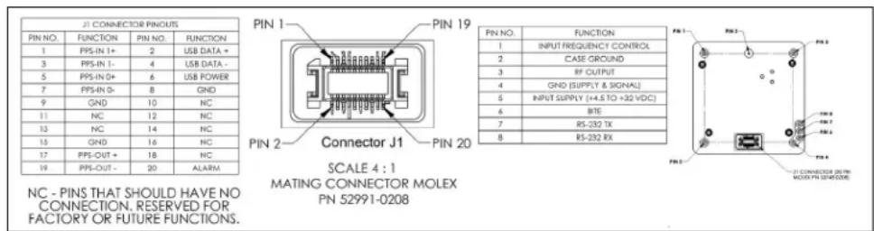
FIGURE 2-3: Pinout.
The electrical function of each pin is shown in Table 2-1.
TABLE 2-1: PIN FUNCTION TABLE
| Connector | Pin Number | Function Range/Format Note | ||
| OCXO Style 1 | Analog tuning input | 0V to 5.0V | Note 1, Note 2 | |
| OCXO Style 2 | Baseplate | — Note 3 | ||
| OCXO Style 3 | RF output | CMOS 3.3V | PP nominal Note 4 | |
| OCXO Style 4 | GND — Note 5 | |||
| OCXO Style 5 | Supply voltage (VCC) | 4.5VDC to 32VDC (5VDC recommended) | — | |
| OCXO Style 6 | Built-In Test Equipment (BITE) | CMOS: Logic_H > 3V, Logic_L < 0.3V | Note 6 | |
| OCXO Style 7, 8 | Serial communication | 2.8V < Logic_H < 3.8V0V < Logic_L < 0.3V | Note 7 | |
| J1 Molex | 1, 3 | PPS1-IN | LVDS | — |
| J1 Molex | 5, 7 | PPS0-IN | LVDS | — |
| J1 Molex | 8, 9, 15 | GND — — | ||
| J1 Molex | 17, 19 | PPS-OUT –,+ | LVDS square wave, 4 ns, 100Ω | — |
| J1 Molex | 20 | Alarm | CMOS: Logic_H > 3V, Logic_L < 0.3V | — |
| J1 Molex | 2, 4, 6 | USB | USB | — |
Note 1: Analog tuning input sensitivity is 0V to 5V into 5 kΩ, 2.5V for no pull.
2: Analog tuning is disabled by default. Digital tuning is recommended instead.
3: Shall be connected to GND externally.
4: 10 MHz, CMOS square wave, VL < 0.3V, VH > 3V. Amplitude is dependent on load.
5: Signal and Supply. It is recommended to tie this ground to same node as baseplate ground Pin 2.
6: BITE output (active-low):
0 = Normal Operation
1 = Unlock Condition
7: If connecting to COM port of a computer, a TTL/RS-232 (or HCMOS/RS-232) adapter is necessary.
2.2.1 Absolute Minimum and Maximum Ratings
Table 2-2 indicates the absolute minimum and maximum ratings to which the MAC can be subjected without permanent unrecoverable damage.
Note: The MAC cannot be expected to perform normally when operated outside of the recommended operating conditions noted on the product data sheet. All ratings apply at +25°C, unless otherwise noted.
TABLE 2-2: MINIMUM AND MAXIMUM RATINGS
| Parameter Rating | |
| Supply Voltage ( VCC ) 0VDC to +32VDC | |
| 1PPS Inputs -0.5V to +3.6V | |
| Analog Tuning Voltage | 0V to +5V (into 5 kΩ) |
| Maximum Current Draw | RS-232, BITE, Alarm: ±8 mARF output: ±8 mA |
| Storage Temperature -55°C to +100°C |
2.3 START-UP SEQUENCE
CAUTION
To avoid severe damage to the unit, do not apply power to the incorrect terminals. The SA5X does not have reverse voltage protection.
When the MAC is initially powered on, it performs an acquisition sequence, which includes stabilizing the temperature of the physics package, optimizing physics package operating parameters, and acquiring frequency lock to the atomic resonance.
A typical warm-up sequence is shown in Figure 2-4. When power is connected to the MAC, its RF and 1PPS output signals (orange dashed line) will appear immediately. The short-term stability specification of these signals will not be satisfied until the Lock sequence is completed (after \~300 seconds in this example). Prior to Lock, the output signal will have an inaccuracy of several ppm and drift per the MAC's internal TCXO.
All MAC's have their (Locked) output frequency calibrated to within ± 5× 10-11Hz / Hz prior to shipment. However, environmental conditions and transit time will affect the calibration to an unknown degree. Therefore, some additional frequency offset should be expected when the MAC is first powered on by the user. Offsets may be corrected, as explained in the Frequency Steering section. The re-trace specification provides some guidance for frequency offsets due to powering off the unit; however, the specification is not comprehensive.
Power consumption is displayed as a solid black trace. Initially, the power consumption will draw >10W to bring the internal unit temperature up to operational level. Once the temperature has stabilized, the steady state power consumption will drop to \~6W. Steady state power consumption will be higher for colder ambient temperatures because more heating will be required to maintain the correct internal temperature. Similarly, the duration of the heat-up period (maximum power consumption) will be longer for colder ambient temperatures.
The baseplate temperature (solid orange trace) will generally rise 15°C during the start-up sequence, but this varies greatly with thermal management (heat sink, airflow, etc). Generally, the temperature rise will be smaller at warmer temperatures, larger at colder temperatures.
Care should be used to ensure that the maximum operating temperature is not violated. For instance, a MAC that is powered up in a 70°C ambient environment will likely rise above the maximum operating temperature during the start-up period unless careful thermal management is employed. (See Section 2.2 "Mounting Considerations")
The LockProgress parameter (not pictured) will reveal the Lock acquisition status in terms of percentage-complete. Once the unit finishes the sequence, the BITE pin (black dashed trace) will indicate Lock (logic low). Generally, Lock acquisition times will be shorter at warmer temperatures, longer at colder temperatures. If this sequence should fail, the Alarms parameter will signify "Acquisition Failed". If this should occur, check that the environmental specifications have not been violated (operating temperature, input voltage, magnetic field exposure, etc) and reboot the device. Contact Customer support if the alarm persists.
Note: Sequence times and power levels vary according to environmental conditions, especially temperature.

FIGURE 2-4: Start-Up Sequence.
Once power is supplied to the unit, it will output the following strings on the serial port:
[>Loading...]
[>Microchip SA5X]
After a typical warm-up time of 5 to 7 minutes, the oscillator is fully operational and the operator may choose to adjust the device parameters. The MAC meets all short-term stability specifications as soon as Lock is achieved. Long-term stability specifications (Monthly Aging frequency drift rate) is satisfied within 30 days of continuous power at room temperature. There are no maintenance procedures or adjustments needed, aside from frequency adjustment which is described in a later section.
Chapter 3. Operation
This section will cover the following topics:
- Configure the Serial Port
- Analog Tuning
• Digital Frequency Adjustment - Configure 1PPS Discipline Settings
- Query the MAC's Health/Lock/Alarm Status
- Configure the Time of Day
3.1 CONFIGURE THE SERIAL PORT
The default settings for the RS-232 interface are listed below.
• Speed: 57600 bps
- Data Bits: 8 bits
- Parity: None
- Stop Bits: 1
- Flow Control: None
The baud rate can be configured via the bootstrap loader (BSL). The following sequence illustrates how to query and set the baud rate. The following interaction sequence begins with the SA5X unit already powered on:
TABLE 3-1: BOOTSTRAP LOADER INTERACTION SEQUENCE
| Serial Communication Description | |
| {reset} User resets the CPU to access the bootloader. | |
| [>Loading...] After reset, BSL announces it is ready (waits 3 seconds). | |
| {bsl} User requests the BSL command mode (within 3 seconds). | |
| [=BSL] BSL confirms it is now in command mode. | |
| {baud?} User queries the currently configured baud rate (optional). | |
| [=57600] | BSL returns the configured baud rate. |
| {baud,921600,now} User requests a new baud rate to take effect immediately.Omission of “,now” argument will defer the change until thenext reset. | |
| [=921600] | BSL confirms the newly configured baud rate. |
| {reset} | User resets the CPU for the new rate to take effect. |
| [>Loading...] After reset, BSL announces its presence at 921600 bps. | |
See Chapter 4. "Command Line Interface" for reference on proper command syntax.
3.2 ANALOG TUNING
Analog tuning allows a user to correct the RF and 1PPS output frequency by applying a DC correction voltage. Analog tuning is an inferior approach compared to Digital tuning or 1PPS Disciplining because its resolution is only parts in 1011 . However, it has been carried forward to support legacy applications.
The analog frequency control is derived from the analog voltage applied to Pin 1. This voltage is digitized, scaled, and applied to the SA5X frequency servo. Analog tuning (AT) voltages above mid-point (2.5VDC) increase the output frequency, and, conversely, tuning voltages below midpoint decrease the output frequency. Because the tuning range is ± 1× 10⁻⁸ from 0V to 5V, this corresponds to roughly 1× 10-11 for every 2.5mV change in AT voltage.
If the analog frequency tuning is disabled (by default), the analog frequency control value is zero. It may be enabled with the AnalogTuningEnabled Parameter. The Analog Tuning input voltage may be read via the AnalogTuning parameter, regardless if it is enabled or not.
Recommendation: If Analog Tuning is the desired method, it is highly recommended that it be used exclusively. Do not try to implement Analog Tuning with Digital Tuning or 1PPS Disciplining simultaneously into one system.
3.3 DIGITAL TUNING
The MAC RF and 1PPS outputs may be adjusted by the user via the DigitalTuning parameter. Relative steering values are entered in (integer) units of parts in 1015 , though the resolution realized by the MAC hardware is approximately 1 part in 1014 . Digital adjustment is clamped to ±2 parts in 108 . Consult Section 3.3.1 “Calibration” if a larger correction is desired.
Note: Steering commands may be entered during acquisition (Locked = 0) but will not take effect until lock is achieved.
Frequency steering is volatile (unless the store command is used). Upon reboot, the MAC returns to its nominal (calibrated) frequency setting. To update the non-volatile calibration, see Section 3.3.1 "Calibration".
3.3.1 Calibration
In the unlikely event that the adjustment range of DigitalTuning has been exhausted beyond the limits of ±2×10⁻⁸ (perhaps due to cumulative frequency aging offsets) it may be desirable to update the calibration. When this is the case, manual calibration of the MAC is accomplished in the following manner. First, the MAC output should be compared to a superior Frequency Reference with a frequency counter or other suitable test equipment. Next, the MAC is steered onto frequency by adjusting the DigitalTuning parameter, (see Section 3.3 “Digital Tuning”) or by enabling Disciplining (see Section 3.4 “1PPS Disciplining”). Finally, the calibrated values of the DigitalTuning and DisciplineTuning parameters are summed into the non-volatile calibration register via the latch command. This command will simultaneously reset DigitalTuning and DisciplineTuning to zero at the new center frequency. The user may then adjust the output ±2×10⁻⁸ from its current value.
Note: Once a calibration is overwritten, it cannot be recalled.
Note: The latch command is only valid when the MAC is locked (Locked = 1).
Note: Total net steering range is limited to ±1×10⁻⁶ . See data sheet for exact specification.
3.4 1PPS DISCIPLINING
For further reduction of phase and frequency errors, disciplining can be enabled/disabled with the Disciplining parameter. The algorithm implements a high-resolution phase meter within the MAC to automatically correct the phase and frequency relative to a reference 1PPS input once per second with a resolution of 450 ps. The algorithm will simultaneously steer the phase and frequency to that of the external reference (1PPS input), ultimately achieving accuracies of <1 ns and 1 × 10-13 , respectively, depending on the stability of the 1PPS input and ignoring external cabling delays, etc (See Section 3.4.5 “Cable Length Compensation”).
3.4.1 Theory
The 1PPS input is user selectable from pins J1-5,7 or J1-1,3 via the PpsSource parameter. If a valid 1PPS is present on the selected input, PpsInDetected = 1 and the user will notice the DisciplineTuning parameter automatically adjust, once Disciplining is enabled. The LastCorrection parameter will tell the user how much the MAC was digitally steered (in frequency) since its last correction; it is simply the difference between the last two successive DisciplineTuning values. Similarly, the Phase parameter will report the most recent phase meter measurement to indicate the time-difference between input and output 1PPS signals.
The speed and effectiveness of the disciplining algorithm can be adjusted by the time constant “Tau”, which is user selectable through the TauPps0 (or TauPps1) parameter. See Section 3.4.2 “Selection of Disciplining Time Constant, “Tau”” for advice on choosing an appropriate time constant.
When disciplining is turned on, it will make a correction once per second based on its most recent internal phase meter measurement. The disciplining algorithm will attempt to dampen an initial phase and/or frequency error E0 by \~63% after an elapsed time of one Tau, 99% after five Tau per the equation:
EQUATION 3-1:
E E _ 0 × (1 - e ^ - t/τ)
Where:
E = The instantaneous error.
E0= The initial error calculated from the moving average of the previous errors observed over time duration τ , updated once per second.
τ = The user-selectable time constant, tau, in seconds.
t = Elapsed time, in seconds.
Any subsequent additional errors after E0 will prolong the settling time of the algorithm.
In the event that the reference 1PPS input is removed from the selected input (pins J1-5,7 or J1-1,3) while disciplining, the MAC remains in holdover and preserves the most recent DisciplineTuning value. If the 1PPS reference subsequently reappears, disciplining continues where it left off. The exception being if the measured instantaneous Phase > PhaseLimit, whereby a JamSync will be implemented and the Disciplining algorithm will start anew.
The status of disciplining is indicated by the DisciplineLocked parameter in the telemetry. DisciplineLocked = 0 upon algorithm startup or when a valid PPS input signal is not detected. DisciplineLocked = 1 when magnitude of the phase measurement is less than the DisciplineThresholdPps0 setting for two time constants of duration (see Section 3.4.2 "Selection of Disciplining Time Constant, "Tau").
The following state diagram provides the concept behind the disciplining and phase-metering algorithms. For more information on phase-metering, see Section 3.4.4 "1PPS Phase Measurement Mode".
![graph TD A["No Input 1PPS (Start)"] -->|1PPS: Detected| B["JamSync"] B -->|1PPS: Lost| A B -->|Phase > Limit| C["Disciplining (Steering)"] C -->|Phase < Threshold (for 2x Tau)| D["Locked (Steering)"] D -->|Phase < Threshold| E["Holdover (No Steering)"] E -->|Phase > Limit| B B -->|PhaseMetering: Ena…](/content/2026/05/958759/images/47baac4b3dcf405b3d9bee29c460310cc28d83be0cd939d29bfd99fbcd40ec6a.jpg)
FIGURE 3-1: PPS State Diagram.
Note: Discipline settings are volatile, that is, not preserved across power cycles unless the store command is used.
Note: The user is allowed to adjust the DigitalTuning parameter while in Disciplining mode. However, this is discouraged because it will prolong and disrupt the disciplining algorithm.
3.4.2 Selection of Disciplining Time Constant, "Tau"
Algorithm performance will be predicated on the selection of the disciplining time constant Tau. When possible, it is advisable to choose a Tau that corresponds to the “least noisy” averaging time of your 1PPS input source. Generally, a longer Tau is required for a noisy 1PPS input reference (such as a simple GPS receiver); shorter Tau is acceptable for stable lab-grade instruments (such as a Cesium Beam Tube). Furthermore, shortening the Tau may be necessary to quickly adjust the MAC if its inherent stability is under influence of external environmental conditions (such as g-forces, rapid temperature changes, etc.).

FIGURE 3-2: Sample ADEV Curves.
Figure 3-2 shows the performance of several frequency references. For optimum Disciplining performance when disciplining to a GNSS reference, a time constant should be selected where the MAC and GNSS ADEV curves intersect ( τ = 25,000 seconds, in this example). In this way, the resulting performance of the Disciplined-MAC will have short and mid-term stability of a free-running MAC, combined with the long-term stability of GNSS.
Note: The above set of curves is very generic and a designer should independently quantify the stability of their own GNSS source. Usually, ADEV information for GNSS receivers is not published because the stability will vary according to a variety of environmental conditions; the designer will have to generate this plot on their own. A rough approximation would be to measure the 1s ADEV performance of a GNSS and extrapolate the curve proportional to 1/ .
NOTICE
Caution should be used when using a longer time constant. Initial frequency errors at the start of Disciplining produce phase errors that will grow proportionally with elapsed time. For slow (long Tau) Disciplining algorithms, the initial errors could grow outside the DisciplineThreshold or PhaseLimit settings before an adequate correction can be made by the algorithm, resulting in a JamSync and DisciplineLocked = 0. Generally, a good Discipline approach is to use a short Tau and larger PhaseLimit to achieve faster initial lock acquisition, then apply a longer Tau to further reduce the MAC's phase and frequency error.
3.4.3 JamSync
When Disciplining is first enabled, the algorithm will implement a JamSync (Observable with the JamSyncing parameter). It will also occur whenever the Phase is beyond the PhaseLimit parameter. JamSync has the effect of phase-aligning the MAC's outgoing 1PPS to the incoming 1PPS once. It has the benefit of speeding up the disciplining routine by quickly synchronizing the output 1PPS after one clock cycle (phase is briefly aligned, but frequency is not). The disciplining algorithm can then continue onward by further refining the frequency and phase errors. However, the drawback of a JamSync is that the user will observe a phase "jump" during the JamSync, rather than a slow steer as predicated by disciplining alone. To avoid said "jump", the user can adjust the PhaseLimit parameter. This is particularly useful for long Disciplining time constants. However, the initial JamSync (when disciplining is initialized) cannot be avoided.
A user may force a JamSync by issuing the sync command (if Disciplining or Phase Measurement mode is enabled).
3.4.4 1PPS Phase Measurement Mode
Phase measurement mode does not steer or Discipline the MAC's output frequency. Rather, it makes use of the MAC's internal phase meter by reporting the time difference between the MAC's internally-generated 1PPS output (pins J1-17,19) and the externally applied reference 1PPS active input (pins J1-5,7 or J1-1,3) once per second. Measurement resolution is approximately 450 ps. The mode is enabled with the PhaseMetering parameter and the internal phase difference can be read via the Phase parameter.
Note: Tau has no effect on the Phase parameter.
3.4.5 Cable Length Compensation
The zero point of disciplining can be adjusted to accommodate cable and other instrumentation delays (or advances) that impact the arrival time of the 1PPS at the MAC 1PPS input pin. The compensation value can be adjusted with the CableDelay parameter.
The maximum compensation adjustment is ±0.5 seconds, where the positive sign indicates phase advancement of the input 1PPS. For example, if there is 45 ns of delay (approximately 33 feet of RG-58 coaxial cable) between the on-time point and the MAC 1PPS input then the compensation value would be +45.
Note: Compensation is implemented in the disciplining algorithm, not in the phase measurement itself. The phase measurement, as reported through telemetry, reports the actual phase measurement. That is, if the MAC is disciplined with +50 ns of compensation, the phase meter reports -50 ns of phase difference when disciplining is settled.
3.4.6 PPS Quantization Error Correction
For use with certain GNSS receivers, the PpsQErr parameter may be used to correct known dynamic quantization errors due to the receiver itself. This is a picosecond adjustment to the next MAC 1PPS phase measurement to account for the error.
3.5 DEVICE INFORMATION AND STATUS
Consult Section 4.4 "Parameters" for a comprehensive list of all available device telemetry parameters. They provide insight into device settings, discipline/atomic lock status, time of day, and alarm conditions.
Several commands provide insight into hardware/software revision, device identification, environmental extremes, and estimated NVRAM health:
- app?
- device?
- platform?
- describe?
- swrev?
- hwrev?
- id?
- serial?
- extremes?
- health?
See Section 4.5 "Commands" for details.
3.6 TIME OF DAY (TOD)
The MAC maintains a TOD parameter TimeOfDay as a 32-bit unsigned integer, which is incremented synchronously with the rising edge of the 1PPS output. Until set otherwise, TOD begins counting from zero when the MAC is powered on.
NOTES:
Chapter 4. Command Line Interface
This section describes the communication interface provided by the Microchip MAC SA5X Rubidium Oscillator. The device supports the Microchip proprietary C3 protocol.
The C3 protocol provides read/write access to the device's parameters. The device's state is exposed through these parameters; modifying their values produces changes in state. The C3 protocol also provides access to flash memory operations, device identification functions, and device telemetry.
Key Features
Key features of the C3 protocol include:
• Text-based: Compatible across many architectures; avoids number representation issues.
- Orthogonal: All commands and responses share the same format.
- Parameter-based: Command set is based on exposing information and controls as a set of parameters.
- Error-detecting: With checksums, garbled commands/responses are more detectable.
Message Flow
For each command message sent to the device, one response message will be returned. In certain situations, such as device startup, announcement messages are sent asynchronously.
Note: Protocol is character case-sensitive.
4.1 COMMAND STRUCTURE
The structure of a C3 command follows:
{command#XX,argument1,|CC}
Where:
TABLE 4-1: COMMAND STRUCTURE
| Field Description Required? | ||
| { Signifies the beginning of a command. Yes | ||
| command The name of the command being issued. Yes | ||
| #XX | The sequence number of the command. (XX = two hex digits). | No |
| ,argument1 | The start of the argument list, beginning with a comma and containing quoted or un-quoted arguments. | Per Command |
| |CC | The 8 bit checksum of the command message. (CC = two hex digits). | No |
| } Signifies the end of a command. | Yes | |
The sequence number, arguments, and checksum fields are optional. If a command is entered incorrectly, MAC will reply with the appropriate error message (See Section 4.2.1 "Error Responses").
Note: Spaces are not used within the command structure.
4.1.1 Sequence Number
The optional sequence number is used to match a response to an earlier command. Commands issued with a sequence number between #01 and #FF will trigger a response message that includes the same sequence number.
4.1.2 Arguments
The argument list follows the command name (or the sequence number, if included), and always begins with a comma before each argument. Numbers and alphanumeric arguments can be written as-is, but arguments that may contain punctuation should be enclosed in double quotes to prevent ambiguity when parsing the command.
Within a quoted argument, the backslash character is a special escape character. It can be used to escape the following sequences (Any other sequences result in the removal of the backslash.):
TABLE 4-2: ESCAPE SEQUENCES
| Escape Sequence Resulting Character | |
| \r Carriage return. | |
| \n New line/line feed. | |
| \t Horizontal tab. | |
| \ Backslash. | |
4.1.3 Command Checksum
An optional 8-bit checksum provides a measure of reliability to commands and responses. If a checksum is included with a command, the response will also include a checksum for verification purposes.
The checksum of a command is calculated as a running XOR of all the characters between the opening ‘{’ and the ‘|’ checksum delimiter. It is a two-byte ASCII representation (in hexadecimal) of the XOR.
{command#XX,argument1,"argument2"|CC}
For example, the hexadecimal checksum of the {device?} command would be entered as:
{device?|27}
If the command is garbled in transmission, causing a mismatch between the contents and the checksum, the C3 response will be [ ! 3 ] indicating a bad checksum error (See Section 4.2.1 "Error Responses"). The command should be re-sent.
4.2 RESPONSE STRUCTURE
The structure of a C3 response follows:
[#XX=value|XX]<CR><LF>
Where:
TABLE 4-3: RESPONSE STRUCTURE
| Field Description Usage | ||
| [ Indicates the start of a response. Always | ||
| #XX | The sequence number in the corresponding command (XX = two hex digits). | Only when a sequence command is sent |
| = | The response type. A normal response type is indicated by a ‘=’ character. An error response is indicated by a ‘!’ character. | Always |
| value | The response value. It may be a number, alphanumeric, or quoted string. The meaning of the value depends upon the command. Max Length is 4096 characters. | Always |
| |CC | The 8-bit checksum of the response message. (CC = two hex digits). | Only when a checksum command is sent |
| ] Indicates the end of a response. Always | ||
| A carriage return character. Always | ||
| A linefeed/newline character. Always | ||
A sequence number will be included in a response if one was provided in the command. Similarly, a checksum will be included in a response if a checksum was given for the command.
4.2.1 Error Responses
An error response indicates a problem with the command. It is identified by a ‘!’ character instead of ‘=’ following the optional message sequence number.
The following table lists all error numbers returned by the device:
TABLE 4-4: ERROR RESPONSES
| Error Number Error Message Cause(s) | ||
| 1 | Invalid command | Unrecognized command name, invalid syntax. |
| 2 | Insufficient arguments | Not enough arguments provided for the command. |
| 3 | Bad checksum | Checksum does not match the message received. |
| 100 | Invalid parameter | The given parameter name or id is unrecognized. |
| 101 | Invalid argument | One of the command arguments was semantically invalid. See the command's documentation for details. |
| 102 | Read-only parameter | The parameter's value cannot be written by the user. |
| 301, 303 | Corrupt file contents | The firmware file contents are corrupted. |
| 302 | Bad file checksum | There was an error in the file transfer. |
| 304 | Incomplete file | The firmware file contents are incomplete. |
| 310 | Transfer failed – too many retries | The file transfer was aborted after too many retries. |
| 311 | Transfer failed – canceled by client | The client aborted the file transfer. |
| Error Number | Error Message Cause(s) | |
| 312 | Synchronization error A file transfer | synchronization error occurred. |
| 313 | Transfer failed –Unsupported request | The file transfer was aborted due to an unsupported request. |
| 320 | Erase failed An error occurred while erasing flash memory. | |
| 321 | Write failed An error occurred while writing to flash memory. | |
For example, the response to the invalid command {type7} would be:
[!1]<CR><LF>
4.2.2 Response Checksum
The checksum of a response is calculated as a running XOR of all the characters between the opening ‘[‘ and the ‘]’ checksum delimiter. See the double underlined portion of the response below:
[#XX=value|CC]<CR><LF>
For example, the checksum-response to the {device?|27} command would be:
[=sa5x|62]<CR><LF>
4.3 ANNOUNCEMENT STRUCTURE
The structure of a C3 announcement follows:
[>message|CC]<CR><LF>
Where:
TABLE 4-5: ANNOUNCEMENT STRUCTURE
| Field Description Usage | ||
| [ Indicates the start of an announcement | Always | |
| > | Identifies this as an announcement, versus a response or error. | Always |
| message | The announcement message. It may be alphanumeric or a quoted string. | Always |
| | CC | The 8-bit checksum of the announcement message.(CC = two hex digits) | Currently unused feature |
| ] Indicates the end of an announcement | Always | |
| CR A carriage return character. | Always | |
| LF A linefeed/newline character. | Always | |
Currently, announcements only occur immediately after applying power to the unit (or resetting the microprocessor):
[>Loading...]<CR><LF>
[>Microchip SA5X]<CR><LF>
4.4 PARAMETERS
The state of the device is exposed as a set of parameters: named values with semantic attributes. Certain parameters are readable/writable to allow the device to be controlled and configured, while other read-only parameters present useful status information.
Parameters are uniquely identified by either a numeric id (e.g. 769) or a name (e.g. PpsSource). The device provides a set of commands to indicate which parameters are available to the user and to describe each one, including name string, real world units, whether it's writable, etc.
4.4.1 Parameter Index
The parameters provided by the device are listed in the table below.
TABLE 4-6: PARAMETER INDEX
| ID Name R/W Description Units | Allowable Range (Note 1) | ||||
| General Status Parameters | |||||
| 256 | Alarms | RO | Bitfield of all active alarm conditions. | Bitfield | 32 bits |
| 257 PpsInDetected RO | A signal is detected on the selected PPS source. | Boolean | 0 or 1 | ||
| 258 | TotalRuntime | RO | Total time powered on (since V1.5) | seconds | 0 to 2,147,483,647 |
| 259 TotalLocktime RO | Total time locked to physics (since V1.5) | seconds | 0 to 2,147,483,647 | ||
| 263 Locked RO | The unit is in a locked and stable state. | Boolean | 0 or 1 | ||
| 264 TimeOfDay | R/W | Time of day at the next 1PPS output pulse. This is a configurable second counter. | seconds | 0 to 2,147,483,647 | |
| 265 DisciplineLocked | RO | Disciplining servo is locked to the selected PPS source. | Boolean | 0 or 1 | |
| Configuration Parameters | |||||
| 512 PpsOffset | R/W | Offset of the output pulse. Default is 0 ns. | ns | ±83,886,080(10 ns step) | |
| 513 PpsWidth | R/W | Width of the output pulse. Default is 20,000 ns. | ns | 0 to 83,886,080(10 ns step) | |
| 515 CableDelay | R/W | 1PPS input cable delay compensation. Default is 0 ns. | ns ±50 | 0,000,000 | |
| Disciplining Parameters | |||||
| 768 Disciplining | R/W | Disciplining to 1PPS input is enabled. Default is false. | Boolean | 0 or 1 | |
| 769 PpsSource | R/W | Selected 1PPS input source:0 = PPS Input 0, 1 = PPS Input 1. Default is 0. | — | 0 or 1 | |
| 770 TauPps0 | R/W | Disciplining time constant when using PPS Input 0. | seconds | 10 to 45,000 | |
| 771 PpsQErr | R/W | Time error of the next input pulse due to quantization. For compatibility with GNSS receivers. | ps ±1,000,000 | ||
| 772 PhaseLimit | R/W | Limit of phase offset between 1PPS input and 1PPS output before jam syncing. Default is 1,000 ns. | ns ±1,000,000 | ||
| 773 JamSyncing | RO | A jam sync to remove phase offset is in progress. | Boolean | 0 or 1 | |
| 774 Phase | RO | Most recent measurement of phase offset between 1PPS input and 1PPS output. | ns ±50 | 0,000,000.0 | |
| ID | Name | R/W | Description | Units | Allowable Range (Note 1) |
| 775 LastCorrection RO | Most recent frequency correction due to disciplining. | x 10-15 | ±20,000,000 | ||
| 777 TauPps1 R/W | Disciplining time constant when using PPS Input 1. | seconds | 10 to 45,000 | ||
| 778 PhaseMetering R/W | Metering of 1PPS phase offset without corrections is enabled. Default is false. Cannot be enabled simultaneously with disciplining. | Boolean | 0 or 1 | ||
| 779 DisciplineThresholdPps0 R/W | Phase threshold for determining a disciplining lock to PPS Input 0. | ns 1 to | 1,000 | ||
| 780 DisciplineThresholdPps1 R/W | Phase threshold for determining a disciplining lock to PPS Input 1. | ns 1 to | 1,000 | ||
| Oscillator Parameters | |||||
| 1288 LaserTempSet RO | Laser temperature setpoint (since V1.5) | m°C 30 | 000 to 70000 | ||
| 1289 OscTuning | RO | Oscillator tuning voltage (since V1.5) | uV | 0 to 3.3e6 | |
| 1291 OvenCurrent | RO | Oven heater current (since V1.5) | uA | 0 to 2.3e6 | |
| 1292 DCSignal | RO | DC signal measurement (since V1.5) | uV | 0 to 2.5e6 | |
| 1293 AnalogTuning RO | The measured analog tuning input voltage. | mV | 0 to 5,000 | ||
| 1296 Temperature | RO | Ambient temperature of the unit. | m°C | -40,000 to 100,000 | |
| 1300 DigitalTuning R/W | Digital tuning of the oscillator frequency. Default is 0. Values are volatile (not preserved across a power-cycle). | x 10-15 | ±20,000,000 | ||
| 1306 PowerSupply | RO | The measured voltage of the external power supply. | mV | 0 to 36,300 | |
| 1312 AnalogTuningEnabled | R/W | Analog tuning is enabled. Default is false. | Boolean | 0 or 1 | |
| 1321 EffectiveTuning | RO | Total effective digital frequency tune. This provides little insight to the user since its value will vary depending upon a number of constantly changing internal adjustments. | x 10-15 | ±2,147,483,647 | |
| 1332 LockProgress | RO | Progress toward acquiring lock. | % | 0 to 100 | |
| 3142 DisciplineTuning | RO | Digital tuning of the oscillator frequency due to the 1 PPS disciplining servo (since V1.1). | x 10-15 | ±2,000,000,000 | |
Note 1: Allowable ranges are integer-only, unless indicated otherwise.
4.4.2 Parameter Attributes
Each parameter has a set of fixed attributes that describe semantic information about itself: read-only, stored to flash, etc. These attributes are represented as a 32-bit field, below.
TABLE 4-7: PARAMETER ATTRIBUTES
| 31-15 | 1 | 4 | 1 | 3 | 1 | 2 | 1 | 1 | 1 | 0 | 9 | 8 | 7 | 6 | 5 |
| — | U n i t s | — | — | — | — | Persisted | — | Silent | Read-Only | — | — | ||||
- Read-Only: The parameter cannot be written by the user.
- Silent: Changes to the value are excluded from the upd command.
- Persisted: This parameter will be written to flash by a store command.
- Units: A 5-bit enumeration containing the parameter's real-world units.
Use the browse command to learn the attributes of each parameter.
4.4.2.1 PARAMETER UNITS ATTRIBUTE
The following table maps Units Attribute values to Parameter units:
TABLE 4-8: UNITS ATTRIBUTE
| Units Value Parameter Units | |
| 0 None/No units | |
| 1 Picoseconds | |
| 2 | Nanoseconds |
| 3 | Microseconds |
| 4 | Milliseconds |
| 5 | Seconds |
| 6 | Microvolts |
| 7 | Millivolts |
| 8 | Microamps |
| 9 | Milliamps |
| 10 | Millidegrees Celsius |
| 11 | x 10-12 |
| 12 | x 10-15 |
| 13 | Hertz |
| 14 | Kilohertz |
| 15 | Megahertz |
| 16 | Percent (%) |
| 17 | Boolean (true/false) |
| 18 | Millimeters |
| 19 | Millimeters/second |
| 20 | Meters |
| 21 | Meters/second |
| 22 | Degrees |
| 23 | Decibel Hertz (dBHz) |
| 24 | Microdegrees Celsius |
| 25 | dBm |
For example, the command {browse, attrs, PpsInDetected} will return [=17412]. This maps to bits 10, 14 as a logic high (indicating a Units Value of "17" or "Boolean") and bit 2 as a logic high (indicating that the parameter is "read only").
4.4.3 Alarms Parameter
The Alarms parameter represents the device's current alarm state as a bitfield. Each 1 bit represents an active alarm condition. The user is also notified of new alarm conditions via the device's ALARM pin (J1-20).
This pin is driven high when a new alarm condition occurs and it remains high until the condition is resolved or the user acknowledges it with the ackalm command. If multiple alarm conditions are unacknowledged by the user, the ALARM pin will remain high until each individual alarm condition has been acknowledged or resolved.
Alarm Bits
The bits of the Alarms parameter are described as follows:
TABLE 4-9: ALARM BITS 31-16
| 31 | 30 | 29 | 28 | 27 | 26 | 25 | 24 | 23 | 22 | 21 | 20 | 19 | 18 | 17 | 16 | |||||||
| — | — | — | — | — | — | — | — | — | — | Disciplining Range Warning | No PPS Input | Temperature Warning |
TABLE 4-10: ALARM BITS 15-0
| 15 | 1 | 4 | 13 | 12 | 11 | 10 | 9 | 8 | 7 | 6 | 5 | 4 | 3 | 2 | 1 | 0 | ||||||||||
| — | — | — | — | — | — | — | — | — | Incompatible Firmware | Heater Fault | No External Oscillator | Acquisition Failed | Flash Fault | PLL Fault | FPGA Fault |
TABLE 4-11: ALARM DESCRIPTIONS
| Bit Decimal Alarm Description | |||
| 0 | 1 | FPGA Fault | Hardware fault related to the internal FPGA. |
| 1 2 | PLL Fault | Hardware fault related to the internal PLL circuit. | |
| 2 4 | Flash Fault | Hardware fault related to flash memory. | |
| 3 | 8 | Acquisition Failed | The most recent attempt to acquire lock failed. |
| 4 | 16 | No External Oscillator | An external oscillator was expected and not detected. |
| 5 | 32 | Cell Heater Fault | Hardware failure within the Cell Heater. |
| 6 | 64 | Incompatible Firmware | The loaded firmware is not compatible with the unit's hardware. |
| 16 | 65536 | Temperature Warning | The clock is unable to maintain a stable internal temperature and performance is likely degraded. This alarm is only asserted when the Locked parameter is 1. |
| 17 13 | 1072 No P | PS Input | Disciplining is enabled but no 1PPS input is detected on the selected input. |
| 18 26 | 2144 | Disciplining Range Warning | Disciplining is enabled but the digital tuning adjustment needed to discipline the clock is outside the range of DigitalTuning. The user should issue a latch command when this alarm occurs. |
4.5 COMMANDS
The Microchip SA5X provides access to all device features, status, and measurements through the C3 command set.
In addition to these standard commands, backwards compatibility with the MAC-SA.3Xm line of Rubidium Oscillators is provided through a set of compatibility commands (See Appendix B. "Legacy Command Set (SA.3Xm)"). Only a subset of the device's functionality is available through the compatibility command interface; it is included to ease the design transition from the SA.3X devices to the newer C3 protocol.
4.5.1 Command Index
The following table contains the available C3 commands. Refer to the next section for detailed command usage.
TABLE 4-12: COMMAND DESCRIPTIONS
| Command | Arguments | Description |
| Device Identification Commands | ||
| app? 0 | Returns a short string identifying the firmware application type. | |
| device? 0 | Returns a short string identifying the device type. | |
| pn? 0 | Returns the unit's part number. | |
| platform? | 0 | Returns a short string identifying the firmware platform of the device. |
| describe? | 0 Returns a readable English description of the device. | |
| swrev? 0 | Returns the software revision. | |
| hwrev? 0 | Returns the hardware revision. | |
| id? 0 | Returns information identifying the product and version. | |
| serial? 0 | Returns the serial number of the unit. | |
| help 0 | Returns a list of available commands. | |
| Parameter Commands | ||
| get 1 | Returns the current value of a parameter. | |
| set 2 | Sets the value of a parameter. | |
| add 2 | Adds to the current value of a parameter. | |
| browse | 1-2 | Returns information about one or more parameters. |
| upd 0 | Returns a list of all parameter values that changed since the last upd. | |
| Alarms Command | ||
| ackalm 1 | Acknowledges an alarm, preventing it from contributing to the ALARM pin state. | |
| Configuration Management Commands | ||
| store | 0 Stores the current configuration to flash memory. | |
| latch | 0 | Latches the current frequency and clears the digital tuning parameter. |
| load 0 | Loads the most recent configuration from flash memory. | |
| Miscellaneous Commands | ||
| sync 0 | Triggers a jam sync, aligning the output 1PPS on the next incoming 1PPS (when the reference is available). | |
| extremes? | 1 | Returns the minimum and maximum measurements for certain parameters over the life of the unit. |
| health? | Returns health estimates of certain components. | |
| reset | 0 Resets the CPU. | |
4.5.2 Command Usage
This section contains command usage and details regarding each supported C3 command, listed in alphabetical order.
{ackalm, alarm}
| Description A | Acknowledges an alarm, or multiple alarms. The acknowledged alarm remains active but it will no longer contribute to the output of the ALARM pin as an outstanding alarm. The value of the Alarms parameter will not be affected; it always shows the active alarms, acknowledged or outstanding. |
| Arguments R | Requires one argument:alarm– The decimal number of alarm bit(s) to acknowledge. Multiple alarm bits may be OR'd together, to be acknowledged simultaneously. |
| Returns [=1] | |
| Since V1.0 |
{add, parameter, amount}
| Description A | Adds to the current value of a parameter. |
| Arguments R | Requires two arguments:parameter– The numeric id or name string of the parameter to modify. Parameter must not be read-only.amount– The amount to add to the value (may be negative). Allowable range depends on parameter used. |
| Returns The | parameter's updated value.Error [!100] (Invalid parameter) if the parameter does not exist.Error [!102] (Read-only parameter) if the parameter is read-only. |
| Since V1.0 |
{app?}
| Description | Returns a short string identifying the firmware application type. |
| Arguments | None. |
| Returns | [=clock] in normal operation, or [=bsl] in the bootstrap loader. |
| Since V1.0 |
{browse, what, parameter}
| Description | Returns information about one or more parameters. |
| Arguments | Accepts two arguments (first is required):what– (Required) The type of parameter information being queried.Acceptable values forwhatare:“id” – Browses numeric parameter ids.“name” – Browses parameter name strings.“value” – Browses current parameter values.“attrs” – Browses parameter attributes.parameter– (Optional) The numeric id or name string of the specific parameter being queried. |
| Returns | A single item (ifparameteris specified), or a list of items beginning with a comma and delimited by commas (ifparameteris omitted). Returned lists are always the same length and in the same order. (e.g. Element N of {browse,id} matches element N of {browse,name}.Error [!101] (Invalid argument) ifwhatvalue for the specified parameter does not exist. |
| Examples | {browse,id} – Returns all parameter IDs.{browse,id,Alarms} – Returns the numeric id of the Alarms parameter. |
| Since V1.0 |
{describe?}
| Description Returns a readable English description of the device. | |
| Arguments None. | |
| Returns A response similar to “Microchip SA5X”. | |
| Since V1.0 | |
{device?}
| Description Returns a short string identifying the device type. | |
| Arguments None. | |
| Returns [=sa5x] | |
| Since V1.0 | |
{extremes?, parameter}
| Description R | Returns minimum and maximum measurements for certain parameters over the life of the unit. The following parameters are supported:TemperaturePowerSupplyAn example command would be {extremes?, Temperature} |
| Arguments R | Requires one argument:parameter– The numeric id or name string of the parameter. |
| Returns The | minimum measurement followed by the maximum measurement, separated by a comma. Example response to the above command would be [=-38389, 83629]...indicating a min and max temperature of -38389 m°C and 83629 m°C.Error [!100] (Invalid parameter) if the parameter does not exist. |
| Since V1.0 |
{get, parameter}
| Description | Returns the current value of a parameter. |
| Arguments | Requires one argument:parameter– The numeric id or name string of the parameter. |
| Returns The | parameter's current value, as an integer or floating-point number.Error [ !100 ] (Invalid parameter) if the parameter does not exist. |
| Since V1.0 |
{health?, component}
| Description R | Returns the health rating of certain components within the unit. Currently, only the flash memory (NVRAM) write endurance is reported. |
| Arguments R | Requires one argument:component– The name of the component to query. Currently, only the nvram component is supported. |
| Returns | The component's health rating, from 0 to 100 (full health). For example [=100] Error [!101] (Invalid argument) if the component is not supported. |
| Since V1.0 |
{help}
| Description R | Returns a comma-delimited list of available commands. Commands that are not accessible with the current authentication will not be included. Some factory-use commands may be included in the list, but are not described in this manual because they present no usable information/function to the user outside of the factory. |
| Arguments None. | |
| Returns A com | mma-delimited list of command names. Example response is:[=,ackalm,add,browse,chap,describe?,extremes?,get,health?,help,hwrev?,latch,load,reset,serial?,session,session?,set,store,swrev?,type?,upd] |
| Since V1.0 | |
{hwrev?}
| Description | Returns the hardware revision of the device. |
| Arguments | None. |
| Returns The | MAC's hardware revision. |
| Since V1.0 |
{id?}
| Description R | Returns a collection of information that identifies the product, as a list of key/value pairs. Key ‘a’ indicates the application name (see the app? command). Key ‘d’ indicates the device type (see the device? command). Key ‘v’ indicates the software version. Key ‘h’ indicates the hardware revision (since V1.5). |
| Arguments None. | |
| Returns Example response:[=,d:sa5x,a:clock,v:V1.5.4.0.63A1D0B2,h:m:089-00891-001;uw:089-00890-000] | |
| Since V1.0 | |
{latch}
| Description S | simultaneously latches the current output frequency and clears the digital tuning. This is used to center the output frequency at the current digital tuning value. The DigitalTuning parameter will be set to zero and the output frequency will be unaffected. Similarly, the DigitalTuning value will be subtracted from the current EffectiveTuning value.Note: The new latched value is preserved across power cycle. |
| Arguments None. | |
| Returns [=1] | |
| Since V1.0 | |
{load}
| Description Loads the most recent configuration from flash memory (Discipline settings, Analog tuning configuration, etc). The device configuration is loaded automatically on boot. | |
| Arguments None. | |
| Returns [=1] | on success.[=0] if no stored configuration is available. |
| Since V1.0 | |
{platform?}
| Description Returns a short string identifying the firmware platform of the device. | |
| Arguments None. | |
| Returns [=sa5x] | |
| Since V1.0 | |
{pn?}
| Description | Returns the part number of the unit. |
| Arguments | None. |
| Returns The | unit's alphanumeric part number, as a text string. |
| Since V1.5 |
{reset}
| Description Resets the CPU. Any un-stored configuration will be lost. The device will reacquire lock on restart. | |
| Arguments None. | |
| Returns No response. Processor is immediately reset. | |
| Since V1.0 | |
{serial?}
| Description Returns the serial number of the unit. | |
| Arguments None. | |
| Returns The unit's alphanumeric serial number as an 11 character text string. | |
| Since V1.0 | |
{set, parameter, value}
| Description Sets the value of a parameter. | |
| Arguments Requires two arguments:parameter– The numeric id or name string of the parameter to modify.value– The new value, as a decimal integer or floating-point number, as allowed by the parameter. | |
| Returns The updated value of the parameter.Error [ !100 ] (Invalid parameter) if the parameter does not exist.Error [ !102 ] (Read-only parameter) if the parameter is read-only. | |
| Since V1.0 | |
{store}
| Description Stores the current configuration to flash memory. The configuration will be loaded automatically on the next restart, or it can be loaded manually with the load command. | |
| Arguments None. | |
| Returns [=1] on success.[=0] on flash memory failure. | |
| Since V1.0 | |
{swrev?}
| Description | Returns the software revisions. |
| Arguments | None. |
| Returns | The revision strings as a comma-delimited list. The first element is the CPU firmware revision. The second element is the FPGA revision.Example response is [=V1.0.4.0.5ADA4E31,V1.0] |
| Since V1.0 |
{sync}
| Description | Triggers a jam sync, aligning the output 1PPS on the next incoming 1PPS (when the reference is available). |
| Arguments None. | |
| Returns [=1] | |
| Since V1.1 | |
{upd}
| Description | Returns a list of all parameter values that changed since the previous upd. This command is useful for collecting telemetry from the device without continuously polling each parameter. Only the values of the parameters that changed will be reported. |
| Arguments None. | |
| Returns A list | of parameter updates notifications, beginning with a comma and delimited by commas. Each notification is composed of two fields, also delimited by commas.The first field in a notification is the id of the parameter that updated. The second field is the parameter's new value.So, if three parameter values have changed since the previous upd command, the returned string will be a list with a total of six values (3 notifications * 2 fields), each preceded by a comma.For example, if the response is [=,513,20000,515,25,779,20] then the PpsWidth, CableDelay, and DisciplineThresholdPps0 parameter values have changed to 20,000 ns, 25 ns, and 20 ns, respectively. |
| Since V1.0 | |
NOTES:
Chapter 5. Maintenance and Troubleshooting
5.1 PREVENTATIVE MAINTENANCE
There are no maintenance procedures or adjustments needed, aside from frequency adjustment. See the product data sheet for environmental requirements.
5.2 ELECTROSTATIC DISCHARGE (ESD) CONSIDERATIONS
Maintenance personnel should wear ESD wrist straps when installing or working on the MAC.
CAUTION
To avoid electrostatic discharge damage, proper ESD handling procedures must be observed in unpacking, assembling, and testing the MAC.
5.3 TROUBLESHOOTING
If the MAC does not respond to user commands, check the following:
- Ensure that the BAUD, flow, and syntax of your terminal interface are configured as described previously.
- Check all physical connections.
- Check that the MAC is not in "compatibility mode". Use the backslash character "\" to exit compatibility mode.
Note: The MAC enters compatibility mode whenever legacy MAC-SA.3Xm commands are entered. It stays in this mode until the user inputs the backslash character “\”.
5.4 REPAIRING THE MAC
The MAC cannot be repaired in the field. It must be sent back to the factory for replacement.
5.5 UPGRADING THE FIRMWARE
As of the initial release of this manual, upgrading the firmware in the field is not supported. It must be sent back to the factory for any future upgrades, if applicable.
5.6 RETURNING THE MAC
You should return the equipment to Microchip only after you have exhausted the troubleshooting procedures described earlier in this chapter, or if Microchip FTS Services and Support has advised you to return the unit.
Note: Please retain the original packaging for re-shipping the product. If the original packaging is not available, contact Microchip FTS Services and Support for assistance.
Repacking the Unit
Return all units in the original packaging. If the original packaging is not available, contact Microchip FTS Services and Support. Use standard packing procedures for products being returned for repair to protect the equipment during shipment.
Connectors should be protected with connector covers or the equipment should be wrapped in plastic before packaging.
Equipment Return Procedure
To return equipment to Microchip for repair:
- Contact Microchip per the guidelines on page 5 to obtain a return material authorization number (RMA) before returning the product for service. You can request an RMA on the internet at: https://microchip.my.site.com/s/ Retain the assigned RMA number for future reference.
- Provide a description of the problem, product item number, serial number, and warranty expiration date.
- Provide the return shipping information (customer field contact, address, telephone number, and so forth.)
- Ship the product to Microchip, transportation prepaid and insured, with the Return Material Authorization (RMA) number and item numbers or part numbers clearly marked on the outside of the container to the address given with the RMA.
Repaired equipment is returned to you with shipping costs prepaid by Microchip.
Appendix A. Principle of Operation
The MAC is a passive atomic clock, incorporating the interrogation technique of Coherent Population Trapping (CPT) and operating upon the D1 optical resonance of atomic 87Rb to control the frequency of a quartz crystal oscillator via a frequency-locked loop (FLL). The FLL function block is shown in Figure A-1. The principal RF output from the MAC is provided by a Temperature-Compensated Crystal Oscillator (TCXO) and provided on the MAC output pin 3.
The laser is mounted on a Thermal-Electric Cooler (TEC) for precise temperature control and is modulated by the microwave synthesizer at half the hyperfine frequency to produce sidebands in the laser spectrum. The light travels through the temperature-controlled Rb cell exposed to a magnetic "C-field" before hitting the photodetector that detects the transmitted CPT resonance signal.
The photodetector current is used to generate a control signal with phase and amplitude information that permits continuous regulation of the TCXO frequency. Servos control frequency synthesis chain, laser current, TEC setpoint, C-field, and cell heater. Additionally, the microprocessor and FPGA provide precise 1 pulse per second functionality.
The main advantage of employing CPT is it allows the use of low power lasers allowing to construct low power, small size atomic clocks.
![graph TD A["DS"] --> B["Microwave Synthesizer"] C["TCKU"] --> B D["Frequency Control"] --> B E["uWavePowerControl"] --> B F["LaserCurrent"] --> B G["TECSet"] --> H["DACDAC"] I["C-Field"] --> J["DACDACAD"] K["CellHeater"] --> L["CellHeater Control"] M["CellHeater"] --> N["DAC"] O["Signal"] --> P["Fil…](/content/2026/05/958759/images/dd559775d93b1b9cc83f7b7a6e33ada974c60a1828b0b2290c73178407243f91.jpg)
FIGURE A-1: Block Diagram.
NOTES:
Appendix B. Legacy Command Set (SA.3Xm)
This section describes the commands used in the Legacy MAC product: SA.3Xm. They have been carried forward to the SA5X product to accommodate legacy applications. These compatibility commands do not follow the aforementioned C3 command syntax; the response syntax is unique to each command. When a compatibility command is received, the Microchip SA5X serial command processor enters “compatibility mode.” An escape character ‘\’ is required to escape the mode before issuing any further C3 commands.
Generally, these commands are considered inferior to the C3 commands and are not recommended for new designs. All of the old commands may be used with the new product and will have the same intended functionality. However, you may see some minor changes in the MAC response to these commands (such as string length or additional data fields).
Any serial port terminal emulator program can be used to communicate with the MAC.
B.1 LEGACY COMMAND STRUCTURE
The legacy SA.3Xm communication protocol supports the following types of commands:
- Single keystroke: A carriage return is not required.
- Multiple keystroke: Requires a specific start (<) and end (>) character. Used for commands that require arguments. A carriage return is not required. All multiple keystroke commands return confirmation strings describing what action they have taken.
The MAC communicates exclusively with "printable" ASCII characters.
All commands produce a response from the MAC, which are human readable, with individual lines ending in a carriage return/line feed sequence. If an unsupported or improperly formatted command is received, the MAC responds with "?" followed by a carriage return/line feed sequence.
Note: The remainder of this document abbreviates “carriage return/line feed” as “[CRLF]”.
B.2 LEGACY COMMAND INDEX
Table B-1 summarizes the Legacy MAC SA.3Xm commands.
TABLE B-1: LEGACY COMMAND INDEX
| Command Description | |
| A Analog | Tuning Enable |
| a Analog | Tuning Disable |
| c Display | Current Values |
| 6 Return | telemetry headers as comma-delimited string |
| ^ Return | telemetry as comma-delimited string |
| Disables analog tuning and persists the setting past power-off | |
| Enables analog tuning and persists the setting past power-off | |
| Apply the Digital Adjustment value to the Center Frequency and zero out the Digital Adjustment value | |
| Save current DDS Center Frequency to Non-volatile memory (NVRAM) | |
| Add nnn to the current DDS Center Frequency. (nnn is in pp 10 12 ) | |
| Add nnn to the current DDS Center Frequency. (nnn is in pp 10 15 ) | |
| Replace the Digital Adjust value with nnn. (nnn is in pp 10 12 ) | |
| Replace the Digital Adjust value with nnn. (nnn is in pp 10 15 ) | |
| Add nnn to the Digital Adjust value. (nnn is in pp 10 12 ) | |
| Add nnn to the Digital Adjust value. (nnn is in pp 10 15 ) | |
B.3 LEGACY COMMAND USAGE
A
Enables analog tuning but does not persist the setting past power-off. This command also returns a confirmation string. See the
a
Disable Analog tuning. See
c
Returns a list of current telemetry values. Example Response:
...CURRENT VALUES...
BITE = 0
Version = V1.0.4
SerialNumber = 1801MX00041
TEC Control (mDegC) = 55177
RF Control (0.1mv) = 20184
DDS Frequency Center Current (0.01Hz) = 0
CellHeaterCurrent (ma) = 418
DCSignal (mv) = 1000
Temperature (mDegC) = 55024
Digital Tuning (0.01Hz) = 3
Digital Tuning (pp15) = 3000000
Analog Tuning On/Off = 0
Analog Tuning (mv) = 1450
Note: BITE = 0 is an indication of Atomic Lock (1 = un-Lock) Analog Tuning = 0 indicates that it is turned off (1 = on)
6
Retrieves the telemetry headers. Response is a comma-delimited string, suitable for importing into spreadsheet programs.
Example Response:
BITE, Version, SerialNumber, TEC Control (mDegC), RF Control (0.1mv), DDS Frequency Center Current (0.01Hz), CellHeaterCurrent (ma), DCSignal (mv), Temperature (mDegC), Digital Tuning (0.01Hz), Analog Tuning On/Off, Analog Tuning (mv), Digital Tuning (pp15)
^
Retrieves the telemetry values. Response is a comma-delimited string, suitable for importing into spreadsheet programs.
Example Response:
0, V1.0.4, 1801MX00041, 55173, 20174, 0, 413, 1000, 55306, 3, 0, 1450, 3000 000
Note: Similar functionality (comma-separated headers and values) is available with the C3 commands using {browse, name} and {browse, value}.
Note: Maximum output string length = 128 characters.
The command disables analog tuning and persists the setting past power-off. See the A command for a non-persistent version.
The command enables Analog Tuning and persists the setting past power-off.
This command has essentially the same function as the new latch command. Previously, for the legacy MAC-SA3x, the purpose of this command was to add the digital adjustment value into the current center frequency value so that the accumulated changes can be saved. The center frequency could then be subsequently saved using the
Save the current DDS center frequency to non-volatile memory (NVRAM). The
Note: This command is redundant with the
Command will increment or decrement the center frequency by the specified number interpreted as pp 1012 . The range of nnn for the
Example:
Functional Response: Center Frequency will decrement by -10×10-12
Example Response: " ...Persistent Frequency Adjustment = -10"
Command has identical function as
Note:
Command will replace the digital adjustment value with the specified number interpreted as pp 1012 . The range of nnn for the
Example:
Functional Response: digital adjustment set to 1000 × 10-12
Example Response: " ...One Time Frequency Adjustment = 1000"
Command will replace the digital adjustment value with the specified number interpreted as pp 10 15 . The range of nnn for the
Note:
Command will augment the digital adjustment, whereas the commands in the previous section replaced the digital adjustment value.
Example:
Functional Response: digital adjustment will decrement by -500 × 10-12
Example Response: " ...One Time Frequency Adjustment = -500"
Command will increment or decrement the digital adjustment by the specified number interpreted as pp 1015 . The range of nnn for the
Note:
Appendix C. Reference Designs
The following schematics are borrowed from the evaluation kit schematic diagram and may contain extra features that are not required by the end-user. Specific applications should modify these schematics according to each systems requirement.
USB Connection
This reference schematic maps a USB-micro connection to the MAC's USB pins J1-2,4,6.

FIGURE C-1: USB Connection.
RS-232 Connection
This reference schematic converts USB-mini signals and maps them to the MAC's RS-232 pins 7 and 8.

FIGURE C-2: RS-232 Schematic.
If a designer wants to use the RS-232 pins without a USB converter, a line driver such as the TI MAX202 or similar device is recommended (shown in Figure C-3). This schematic was implemented on the previous generation evaluation board and is not featured on the current design.
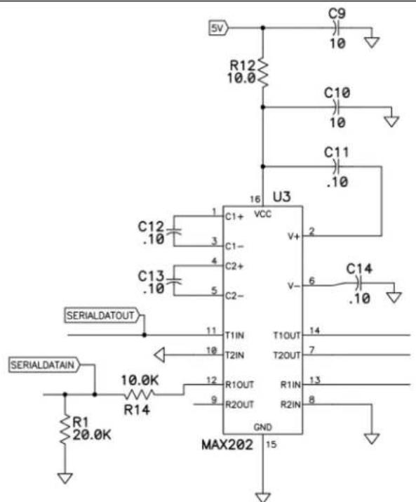
FIGURE C-3: RS-232 Schematic without USB Converter.
1PPS Input Connection
This reference schematic converts a single-ended (3.3V @ 50Ω) 1PPS signal to the differential LVDS format required by the MAC.
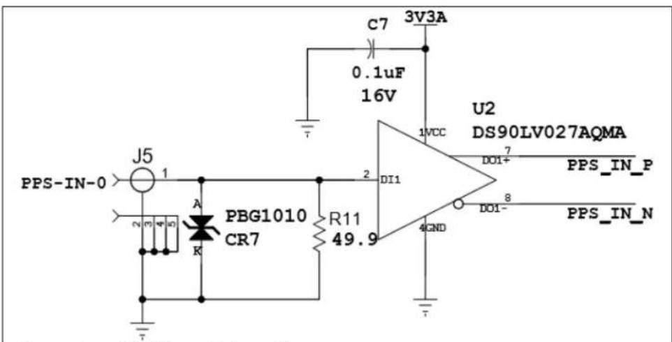
FIGURE C-4: 1PPS Input Schematic.
Analog Tune Input Connection
This reference schematic shows how the Evaluation kit maps AT voltages to the MAC.

FIGURE C-5: Analog Tune Schematic.
1PPS Output Connection
This reference schematic converts the MAC's differential 1PPS LVDS output to a single-ended 3.3V signal and contains a driver circuit capable of driving a 50Ω coaxial cable.

FIGURE C-6: 1PPS Output Schematic.
RF (10 MHz) Output Connection
This reference schematic buffers the MAC's RF output as a 50Ω, 3.3V signal on J2.

FIGURE C-7: RF Output Schematic.
Appendix D. Evaluation Kit
The evaluation kit (p/n 090-44500-000) may be purchased separately and is provided as a means for a user to quickly test out the features of the MAC-SA5X. It is intended for static, bench-top use and is not designed for environmental testing.

FIGURE D-1: Evaluation Board.
D.1 OVERVIEW AND KEY FEATURES
The Evaluation Kit has the following features:
• 10 MHz LVCMOS Output via SMA(f) Connector
• 1PPS Disciplining (Steering) via Two Selectable SMA(f) Connectors
• 1PPS LVCMOS Output via SMA(f) Connector
- -40°C to +75°C Operating Temperature (Baseplate)
- -55°C to +100°C Storage Temperature
- Interface for Digital Steering, Configuration, and Diagnostics via: - USB-mini Communication Port for Accessing RS-232 MAC Pins - USB-micro Communication Port for Accessing USB MAC Pins
• Wall-Plug Power Connector with On/Off Toggle Switch
- Alternate Wide Range Allowable DC Input (4.5V to 32V) Connector
- Heat Sink and Thermal Pad for Thermal Conditioning
• LED Status Indications for Power, Lock, and Alarm
- Insertable Socket Design to Quickly Plug in a MAC without Need for Soldering
• Analog Tuning via SMA(f) Connector
D.2 PHYSICAL DESCRIPTION
The Evaluation Kit contains the following items:
TABLE D-1: EVALUATION KIT CONTENTS
| Description Purpose | |
| #2-56UNC-2A X 31LG type screw (Qty = 4) Fasten MAC-SA5X to Evaluation Board | |
| Wall-mount power adapter US (90VAC to 264VAC) to 5VDC | Supply Power to the MAC and Evaluation board (PS1 connector) |
| USB 2.0(M) to USB-mini(M) cable | Connection from a PC to Evaluation board's serial-to-USB-mini adapter |
| Thermal Pad (p/n 172-00054-000) | Provide thermal interface between MAC and heat sink |
| PCBA/Baseplate Subassembly | Heat sink and PCBA receptacle containing all connections |
The PCBA/Baseplate consists of a 3.9" x 5.1" aluminum heat sink/baseplate attached to a PCBA with six mounting screws. All connections are on the PCBA. The physical connections of the PCBA/Baseplate are highlighted in Figure D-2.

FIGURE D-2: PCBA/Baseplate Physical Connections.
- A power on/off toggle switch is within the red-dashed box.
- Power input connections are identified by red-dashed arrows.
- Input connections are identified by solid-red arrows and are accessible with SMA(f) RF connectors.
- Output connections are identified by green arrows and are also accessible with SMA(f) RF connectors.
- Blue arrows identify the communications ports (accessible with USB-micro and USB-mini).
- Blue boxes highlight the communications LEDs.
- A MAC-SA5X may be plugged into the purple box with its J1 connector oriented towards the bottom of the Evaluation board so that it mates with the Evaluation board's J9 connector.
TABLE D-2: CONNECTIONS
| Eval Board ID | Label Function | Maps to MAC Pin |
| J7 Analog Tune | (INPUT) Accepts DC voltage for frequency steering | 1 |
| J5 PPS_in_0 | (INPUT) Accepts a 1PPS (3.3V, 50Ω) signal for Freq/Phase Disciplining | J1-5,7 |
| J6 PPS_in_1 | (INPUT) Accepts a 1PPS (3.3V, 50Ω) signal for Freq/Phase Disciplining | J1-1,3 |
| J2 10 MHz | (OUTPUT) Buffered MAC RF output (3.3V, 50Ω) | 3 |
| J3 BITE/Lock | (OUTPUT) MAC Lock status (CMOS, 1 MΩ) | 6 |
| J4 PPS_out | (OUTPUT) Buffered MAC 1PPS output signal (3.3V, LVCMOS, 50Ω) | J1-17,19 |
| J1 RS-232 | (COMM.) access the MAC's serial communication port | 7,8 |
| J8 USB-micro | (COMM.) access the MAC's high-speed USB communication port | J1-2,4,6 |
| PS1 5VDC Power | (POWER) accepts the 5VDC wall-mount power adapter for powering the Evaluation board and the MAC | 5 |
| J10 Wide Voltage Input | (POWER) accepts an alternate source of voltage for the MAC (only) if J11 jumpers are removed | 5 |
| SW1 Toggle Switch | (SWITCH) allows power to flow to the Evaluation board from the 5VDC supply | N/A |
| DS3 Power Status | (LED) illuminates when power is provided to PS1 | N/A |
| DS1 Alarm Status | (LED) illuminates when an alarm condition is triggered | J1-20 |
| DS2 Lock Status | (LED) illuminates when Atomic Lock is achieved | 6 |
D.2.1 Communications Connections
The Evaluation board has two USB connections for communicating between a PC and a MAC-SA5X (blue arrows in Figure D-2). The "RS-232" connection accepts a USB-mini(M) connector that then passes to a serial converter on the Evaluation board and applies the appropriate levels on pins 7,8 of the MAC. A USB 2.0-to-USB-mini cable is provided in the kit.
The "USB-micro" connection accepts a USB-micro(M) connector that maps to pins J1-2,4 of the MAC. A cable is not provided in the kit.
Consult the main portion of the MAC-SA5X User Guide for advice on communicating with a MAC plugged in to the Evaluation board.
Three LEDs communicate status information to the user by illuminating under the following conditions:
- Power Status LED illuminates when power is provided to PS1.
- Alarm Status LED illuminates when an alarm condition is triggered.
- Lock Status LED illuminates when Atomic Lock is achieved.
D.2.2 Input Connections
Three input connections are available via SMA connectors on the top of the Evaluation board. The “Analog Tune” connector accepts a DC voltage (see Section 3.2 “Analog Tuning”) for steering the RF (and PPS outputs). This pin maps to pin 1 on the inserted MAC device.
Two 1PPS input connections are available ("PPS_in_0" and "PPS_in_1") for disciplining the MAC's output frequency. The Evaluation board accepts a 3.3V @ 50Ω LVCMOS 1PPS signal. See Section 3.4 "1PPS Disciplining" for details.
D.2.3 Output Connections
Three SMA(f) connectors provide outputs from the MAC's 10 MHZ, 1PPS_out, and BITE/Lock pins. The 10 MHz and 1PPS are buffered according to the schematics in Appendix D and designed to drive 50Ω, while the BITE/Lock pin maps directly to the SMA. See Section 1.2.3 "Output Connections" for more details.
D.2.4 Power Connections
The Evaluation board is supplied with a wall-mount power supply capable of powering the ICs on the board (through "PS1") as well as a MAC inserted into the board. The toggle switch "SW1" controls the flow of power to the board.
Alternatively, one may use the wide voltage range connector "J10" if they wish to test a MAC under variable voltage conditions.
Note: The J11 jumpers must be removed in this mode of operation. Also, the 5V wall-mount supply must still be employed in order to power the other ICs on the Evaluation board.
D.2.5 Functional Description and Operation
CAUTION
To avoid electrostatic discharge (ESD) damage, proper ESD handling procedures must be observed in unpacking, assembling, and testing the MAC.
The MAC and Evaluation board are delivered in ESD-safe packaging. They must be removed from the ESD-protective bag in an ESD-safe environment. Once installed on the test fixture, it is recommended that the entire assembly be treated as ESD-sensitive.
Retain the original MAC ESD-safe packaging material in the event that the device needs to be returned to Microchip for service.
The Evaluation board accepts a MAC-SA5X device using sockets that do not require the use of solder. Four screws are provided to ensure the device remains properly seated on the board. Care should be afforded and the number of insertions should be minimized in order to maximize the lifetime of the sockets and the J9 connector. The Evaluation board is not designed for repeated production-type testing.
Once a MAC is inserted and the wall-mount power supply is connected, the toggle switch may be flipped to supply power to the MAC. The user should expect the "Power Status" LED to illuminate and the communication ports will become active. RF and 1PPS outputs are immediately available after supplying power.
A terminal emulation program may be used to configure and observe the MAC telemetry by connecting a PC to J1 or J8 of the Evaluation board (see
Section 3.1 "Configure the Serial Port"). Once power is supplied to the MAC, it will
behave as outlined in Section 2.3 "Start-Up Sequence". After several minutes, the user should expect the "Lock Status" LED to illuminate, indicating that Atomic Lock has been achieved, and the short-term stability performance of the MAC will behave per the product specifications. Also, the BITE/Lock pin (J3) will flip to a logic zero once Lock is achieved.
Settings such as turning on/off Analog Tuning, Digital Tuning, and 1PPS disciplining can all be adjusted with terminal emulation software. See Chapter 4. "Command Line Interface" for appropriate syntax.
See the sections above regarding appropriate expected input/output signal levels from the Evaluation board. The levels in Appendix D take precedence over other sections of this User Guide that pertain to the MAC-SA5X only.
D.2.5.1 TROUBLESHOOTING
If an error should occur, the "Alarm Status" LED will illuminate. This pin is driven low when a new alarm condition occurs and it remains low until the condition is resolved or the user acknowledges it with the ackalm command. If an alarm cannot be cleared, contact the factory for guidance.
If communication cannot be achieved, ensure the MAC is properly seated and that the communication port settings are appropriate.
If the LEDs do not illuminate, check the power cable connector and toggle switch for damage.
If atomic Lock cannot be achieved, check that the environmental conditions are within product specifications and that the MAC is properly seated on the board.
NOTES:
Appendix E. Software License Agreements
Portions of the SA5X software make use of the following open source software:
FreeRTOS Kernel, Copyright © 2019 Amazon.com, Inc. or its affiliates. All Rights Reserved.
Permission is hereby granted, free of charge, to any person obtaining a copy of this software and associated documentation files (the "Software"), to deal in the Software without restriction, including without limitation the rights to use, copy, modify, merge, publish, distribute, sublicense, and/or sell copies of the Software, and to permit persons to whom the Software is furnished to do so, subject to the following conditions:
The above copyright notice and this permission notice shall be included in all
copies or substantial portions of the Software.
THE SOFTWARE IS PROVIDED "AS IS", WITHOUT WARRANTY OF ANY KIND, EXPRESS OR IMPLIED, INCLUDING BUT NOT LIMITED TO THE WARRANTIES OF MERCHANTABILITY, FITNESS FOR A PARTICULAR PURPOSE AND NONINFRINGEMENT. IN NO EVENT SHALL THE AUTHORS OR COPYRIGHT HOLDERS BE LIABLE FOR ANY CLAIM, DAMAGES OR OTHER LIABILITY, WHETHER IN AN ACTION OF CONTRACT, TORT OR OTHERWISE, ARISING FROM, OUT OF OR IN CONNECTION WITH THE SOFTWARE OR THE USE OR OTHER DEALINGS IN THE SOFTWARE.
NOTES:
Worldwide Sales and Service
AMERICAS
Corporate Office
2355 West Chandler Blvd.
Chandler, AZ 85224-6199
Tel: 480-792-7200
Fax: 480-792-7277
Technical Support:
http://www.microchip.com/
support
Web Address:
www.microchip.com
Atlanta
Duluth, GA
Tel: 678-957-9614
Fax: 678-957-1455
Austin, TX
Tel: 512-257-3370
Boston
Westborough, MA
Tel: 774-760-0087
Fax: 774-760-0088
Chicago
Itasca, IL
Tel: 630-285-0071
Fax: 630-285-0075
Dallas
Addison, TX
Tel: 972-818-7423
Fax: 972-818-2924
Detroit
Novi, MI
Tel: 248-848-4000
Houston, TX
Tel: 281-894-5983
Indianapolis
Noblesville, IN
Tel: 317-773-8323
Fax: 317-773-5453
Tel: 317-536-2380
Los Angeles
Mission Viejo, CA
Tel: 949-462-9523
Fax: 949-462-9608
Tel: 951-273-7800
Raleigh, NC
Tel: 919-844-7510
New York, NY
Tel: 631-435-6000
San Jose, CA
Tel: 408-735-9110
Tel: 408-436-4270
Canada - Toror
Tel: 905-695-1980
Fax: 905-695-2078
ASIA/PACIFIC
Australia - Sydney
Tel: 61-2-9868-6733
China - Beijing
Tel: 86-10-8569-7000
China - Chengdu
Tel: 86-28-8665-5511
China - Chongqing
Tel: 86-23-8980-9588
China - Dongguan
Tel: 86-769-8702-9880
China - Guangzhou
Tel: 86-20-8755-8029
China - Hangzhou
Tel: 86-571-8792-8115
China - Hong Kong SAR
Tel: 852-2943-5100
China - Nanjing
Tel: 86-25-8473-2460
China - Qingdao
Tel: 86-532-8502-7355
China - Shanghai
Tel: 86-21-3326-8000
China - Shenyang
Tel: 86-24-2334-2829
China - Shenzhen
Tel: 86-755-8864-2200
China - Suzhou
Tel: 86-186-6233-1526
China - Wuhan
Tel: 86-27-5980-5300
China - Xian
Tel: 86-29-8833-7252
China - Xiamen
Tel: 86-592-2388138
China - Zhuhai
Tel: 86-756-3210040
ASIA/PACIFIC
India - Bangalore
Tel: 91-80-3090-4444
India - New Delhi
Tel: 91-11-4160-8631
India - Pune
Tel: 91-20-4121-0141
Japan - Osaka
Tel: 81-6-6152-7160
Japan - Tokyo
Tel: 81-3-6880-3770
Korea - Daegu
Tel: 82-53-744-4301
Korea - Seoul
Tel: 82-2-554-7200
Malaysia - Kuala Lumpur
Tel: 60-3-7651-7906
Malaysia - Penang
Tel: 60-4-227-8870
Philippines - Manila
Tel: 63-2-634-9065
Singapore
Tel: 65-6334-8870
Taiwan - Hsin Chu
Tel: 886-3-577-8366
Taiwan - Kaohsiung
Tel: 886-7-213-7830
Taiwan - Taipei
Tel: 886-2-2508-8600
Thailand - Bangkok
Tel: 66-2-694-1351
Tel: 43-7242-2244-39
Fax: 43-7242-2244-393
Denmark - Copenhagen
Tel: 45-4485-5910
Fax: 45-4485-2829
Finland - Espoo
Tel: 358-9-4520-820
France - Paris
Tel: 33-1-69-53-63-20
Fax: 33-1-69-30-90-79
Germany - Garching
Tel: 49-8931-9700
Germany - Haan
Tel: 49-2129-3766400
Germany - Heilbronn
Tel: 49-7131-72400
Germany - Karlsruhe
Tel: 49-721-625370
Germany - Munich
Tel: 49-89-627-144-0
Fax: 49-89-627-144-44
Germany - Rosenheim
Tel: 49-8031-354-560
Israel - Ra'anana
Tel: 972-9-744-7705
Italy - Milan
Tel: 39-0331-742611
Fax: 39-0331-466781
Italy - Padova
Tel: 39-049-7625286
Netherlands - Drunen
Tel: 31-416-690399
Fax: 31-416-690340
Norway - Trondheim
Tel: 47-7288-4388
Poland - Warsaw
Tel: 48-22-3325737
Romania - Bucharest
Tel: 40-21-407-87-50
Spain - Madrid
Tel: 34-91-708-08-90
Fax: 34-91-708-08-91
Sweden - Gothenberg
Tel: 46-31-704-60-40
Sweden - Stockholm
Tel: 46-8-5090-4654
UK - Wokingham
Tel: 44-118-921-5800
Fax: 44-118-921-5820

- NOTE THE FOLLOWING DETAILS OF THE CODE PROTECTION FEATURE ON MICROCHIP PRODUCTS
- TRADEMARKS
- PREFACE
- NOTICE TO CUSTOMERS
- PURPOSE OF THIS GUIDE
- WHO SHOULD READ THIS GUIDE
- DOCUMENT LAYOUT
- CONVENTIONS USED IN THIS GUIDE
- WARNINGS, CAUTIONS, RECOMMENDATIONS, AND NOTES
- WARNING
- CAUTION
- WHERE TO FIND ANSWERS TO PRODUCT AND DOCUMENT QUESTIONS
- RELATED DOCUMENTS AND INFORMATION
- NORTH AND SOUTH AMERICA
- EUROPE, MIDDLE EAST, AND AFRICA (EMEA)
- THE MICROCHIP WEBSITE
- CUSTOMER SUPPORT
- DOCUMENT REVISION HISTORY
- REVISION A (NOVEMBER 2019)
- REVISION B (MARCH 2021)
- REVISION C (DECEMBER 2022)
- REVISION D (JULY 2023)
- REVISION E (APRIL 2024)
- TABLE OF CONTENTS
- PREFACE 3
- CHAPTER 1. PRODUCT OVERVIEW
- CHAPTER 2. INSTALLATION
- CHAPTER 3. OPERATION
- CHAPTER 4. COMMAND LINE INTERFACE
- CHAPTER 5. MAINTENANCE AND TROUBLESHOOTING
- APPENDIX A. PRINCIPLE OF OPERATION....47
- APPENDIX B. LEGACY COMMAND SET (SA.3XM)
- APPENDIX C. REFERENCE DESIGNS ....53
- APPENDIX D. EVALUATION KIT
- APPENDIX E. SOFTWARE LICENSE AGREEMENTS 63
- WORLDWIDE SALES AND SERVICE 65
- 1.1 MAC-SA5X OVERVIEW
- 1.1.1 KEY FEATURES
- 1.2 PHYSICAL DESCRIPTION
- 1.2.1 COMMUNICATIONS CONNECTIONS
- 1.2.2 INPUT CONNECTIONS
- 1.2.3 OUTPUT CONNECTIONS
- 1.2.4 POWER AND GROUND CONNECTIONS
- 1.3 FUNCTIONAL DESCRIPTION
- COMMUNICATION PORTS
- ANALOG TUNING INPUT
- 1PPS INPUTS
- 10 MHZ OUTPUT
- 1PPS OUTPUT
- BITE OUTPUT
- ALARM OUTPUT
- 1.4 CONFIGURATION MANAGEMENT
- 1.5 ALARMS
- 2.1 HANDLING CONSIDERATIONS
- 2.2 MOUNTING CONSIDERATIONS
- SOLDER
- HEAT SINK AND THERMAL MANAGEMENT
- RF NOISE MITIGATION
- EMI AND NOISE CONSIDERATIONS
- SIGNAL CONNECTIONS
- 2.2.1 ABSOLUTE MINIMUM AND MAXIMUM RATINGS
- 2.3 START-UP SEQUENCE
- 3.1 CONFIGURE THE SERIAL PORT
- 3.2 ANALOG TUNING
- 3.3 DIGITAL TUNING
- 3.3.1 CALIBRATION
- 3.4 1PPS DISCIPLINING
- 3.4.1 THEORY
- EQUATION 3-1
- 3.4.2 SELECTION OF DISCIPLINING TIME CONSTANT, "TAU
- NOTICE
- 3.4.3 JAMSYNC
- 3.4.4 1PPS PHASE MEASUREMENT MODE
- 3.4.5 CABLE LENGTH COMPENSATION
- 3.4.6 PPS QUANTIZATION ERROR CORRECTION
- 3.5 DEVICE INFORMATION AND STATUS
- 3.6 TIME OF DAY (TOD)
- KEY FEATURES
- MESSAGE FLOW
- 4.1 COMMAND STRUCTURE
- 4.1.1 SEQUENCE NUMBER
- 4.1.2 ARGUMENTS
- 4.1.3 COMMAND CHECKSUM
- 4.2 RESPONSE STRUCTURE
- 4.2.1 ERROR RESPONSES
- 4.2.2 RESPONSE CHECKSUM
- 4.3 ANNOUNCEMENT STRUCTURE
- 4.4 PARAMETERS
- 4.4.1 PARAMETER INDEX
- 4.4.2 PARAMETER ATTRIBUTES
- 4.4.2.1 PARAMETER UNITS ATTRIBUTE
- 4.4.3 ALARMS PARAMETER
- ALARM BITS
- 4.5 COMMANDS
- 4.5.1 COMMAND INDEX
- 4.5.2 COMMAND USAGE
- 5.1 PREVENTATIVE MAINTENANCE
- 5.2 ELECTROSTATIC DISCHARGE (ESD) CONSIDERATIONS
- 5.3 TROUBLESHOOTING
- 5.4 REPAIRING THE MAC
- 5.5 UPGRADING THE FIRMWARE
- 5.6 RETURNING THE MAC
- REPACKING THE UNIT
- EQUIPMENT RETURN PROCEDURE
- APPENDIX A. PRINCIPLE OF OPERATION
- B.1 LEGACY COMMAND STRUCTURE
- B.2 LEGACY COMMAND INDEX
- B.3 LEGACY COMMAND USAGE
- APPENDIX C. REFERENCE DESIGNS
- USB CONNECTION
- RS-232 CONNECTION
- 1PPS INPUT CONNECTION
- ANALOG TUNE INPUT CONNECTION
- 1PPS OUTPUT CONNECTION
- D.1 OVERVIEW AND KEY FEATURES
- D.2 PHYSICAL DESCRIPTION
- D.2.1 COMMUNICATIONS CONNECTIONS
- D.2.2 INPUT CONNECTIONS
- D.2.3 OUTPUT CONNECTIONS
- D.2.4 POWER CONNECTIONS
- D.2.5 FUNCTIONAL DESCRIPTION AND OPERATION
- D.2.5.1 TROUBLESHOOTING
- APPENDIX E. SOFTWARE LICENSE AGREEMENTS
- WORLDWIDE SALES AND SERVICE
- AMERICAS
- ASIA/PACIFIC
Brand : Microchip
Model : MAC-SA5X-KIT
Category : Horloge atomique