
Joule 550x Compute Module - Computer module INTEL - Free user manual and instructions
Find the device manual for free Joule 550x Compute Module INTEL in PDF.


| Type of Product | Compute Module |
| Brand | Intel |
| Model | Joule 550x |
| Processor | Intel Atom Processor (Quad-core, up to 2.4 GHz) |
| Memory | 4GB LPDDR4 RAM |
| Storage | 16GB eMMC Flash |
| Dimensions | Approximately 100 mm x 70 mm x 20 mm |
| Weight | Approximately 100 g |
| Power Supply | 12V DC, 2A (via barrel jack or USB-C) |
| Operating System Support | Windows 10 IoT Core, Ubuntu 16.04 LTS, Yocto Linux |
| Main Functions | Embedded computing, IoT gateway, robotics, AI inference |
| Connectivity | Gigabit Ethernet, Wi-Fi 802.11ac, Bluetooth 4.1, USB 3.0 |
| Video Output | HDMI 1.4b, MIPI-DSI (dual) |
| Expansion Interface | 40-pin GPIO header, PCIe Gen 2 |
| Cooling | Passive heatsink (active fan optional for high loads) |
| Operating Temperature | 0°C to 60°C |
| Maintenance & Cleaning | Use dry cloth to remove dust; avoid liquids; ensure ventilation is unobstructed |
| Safety | Use only supplied power adapter; do not expose to moisture or static discharge |
| Spare Parts & Repairability | Not user-serviceable; contact Intel support for hardware issues |
| General Information | Developer kit for rapid prototyping and edge computing applications |
Frequently Asked Questions - Joule 550x Compute Module INTEL
User questions about Joule 550x Compute Module INTEL
0 question about this device. Answer the ones you know or ask your own.
Ask a new question about this device
Download the instructions for your Computer module in PDF format for free! Find your manual Joule 550x Compute Module - INTEL and take your electronic device back in hand. On this page are published all the documents necessary for the use of your device. Joule 550x Compute Module by INTEL.
USER MANUAL Joule 550x Compute Module INTEL
No license (express or implied, by estoppel or otherwise) to any intellectual property rights is granted by this document.
This document contains information on products, services, and/or processes in development. All information provided here is subject to change without notice. Contact your Intel representative to obtain the latest forecast, schedule, specifications, and roadmaps.
The products and services described may contain defects or errors known as errata, which may cause deviations from published specifications. Current characterized errata are available on request.
You may not use or facilitate the use of this document in connection with any infringement or other legal analysis concerning Intel products described herein. You agree to grant Intel a nonexclusive, royalty-free license to any patent claim thereafter drafted that includes subject matter disclosed herein.
Intel does not control or audit third-party benchmark data or the web sites referenced in this document. You should visit the referenced web site and confirm whether referenced data are accurate.
Intel technologies may require enabled hardware, specific software, or services activation. Check with your system manufacturer or retailer.
Copies of documents that have an order number and are referenced in this document may be obtained by calling 1-800-548-4725 or by visiting www.intel.com/design/literature.htm.
The Intel Joule Module, Intel and the Intel logo are trademarks of Intel Corporation in the United States and other countries.
*Other names and brands may be claimed as the property of others.
Copyright © 2017 Intel Corporation. All rights reserved
Revision History
| Revision Description Date | ||
| 1.3 | Corrected Bluetooth version to 4.2 on page 10 | January 2017 |
| 1.2 • Updated required strapping tableEdited video encoder InformationAdded links to reference documentsRemoved GPIO mapping for Linux* and po Inted the reader to the website for this informationIncorporated QA format suggestions. | January 2017 | |
| 1.1 Update wireless communication statement forend-use equipment integration September 2016 | ||
| 1.0 Initial release August 2016 | ||
Contents
1 Introduction....8
1.1 Acronyms....8
1.2 Reference documents 9
2 System on Module Overview 9
2.1 Intel® Joule™ module configurations....9
2.2 Intel® Joule™ compute module feature summary....10
2.3 Expansion board requirements ....10
2.3.1 Method for connecting module to expansion board 10
2.3.2 Method to provide +VSYS power to the module 10
2.3.3 Required strapping of module pins 11
2.3.4 BIOS installed onto module....11
2.4 Expansion board recommendations....11
2.4.1 External EEPROM for multipurpose pin configuration data....11
2.4.2 Power button 11
2.4.3 DnX button....11
2.4.4 Real time clock (RTC) backup power source 11
2.4.5 UART debugging....11
3 Power Delivery, Signaling, and Reset 12
3.1 Main power supply (VSYS)....12
3.2 Power on signaling 12
3.2.1 +VDC_IN power sensing....12
3.2.2 +VBUS power sensing....12
3.2.3 Power good 12
3.3 Hard shutdown via power button 12
3.4 System voltage rail specifications ....13
4 Graphics Specifications....13
4.1 Intel® Gen9LP features ....13
4.2 Graphic encoder and decoder support 14
4.3 HDMI* signal group specifications ....14
5 Wireless Connectivity....15
5.1 Intel ^® Dual Band Wireless-AC 8260 highlights....15
5.1.1 Wi-Fi features ....15
5.2 Bluetooth ^® highlights 15
5.2.1 Supported Bluetooth ^ profiles .....15
5.3 Security....16
5.4 Wireless antenna connectors....16
5.5 The Intel ^® Dual Band Wireless-AC 8260 support site....16
6 SD Card Interface....17
6.1 SD card interface features....17
6.1.1 SD card signal group specifications ....17
7 Module Connectors....17
7.1 Module dimensions....17
7.2 Module to expansion board connectors .....18
7.2.1 Module electrostatic discharge....18
7.2.2 J6 connector interface signals 18
7.2.3 J7 connector interface signals 20
8 I2C Interfaces....22
8.1 I2C features 22
8.2 I2C default configuration....22
8.3 I2C signal group specifications....22
9 Clock Specifications....22
9.1 RTC backup battery....22
10 UART Specifications....23
10.1 UART availability 23
11 I2S Specifications 23
11.1 I2S signal group specifications 23
11.1.1 I2S available formats ....23
11.2 Digital microphone ports 24
12 GPIO Specifications....24
12.1 Dedicated GPIO lines 24
12.2 Reconfigurable interfaces buses as GPIO 24
12.3 GPIO internal pull UP / pull DOWN resistors 24
12.4 Operating System GPIO to function mapping....24
13 Pulse Width Modulators 24
13.1 PWM frequency formula: 25
13.2 PWM duty cycle formula: 25
14 Universal Serial Bus 25
14.1 Available USB ports 25
Tables
1 Acronyms and terminology 8
2 Intel® Joule™ module configurations 9
3 Intel® Joule™ compute module features ....10
4 Required strapping of module pins ....11
5 Boot decision per voltage supply condition ....12
6 Module power rails....13
7 Graphics engine encoders and decoders supported....14
8 J6 connector pin descriptions ....18
9 J7 connector pin descriptions 20
10 I2C mapping....22
11 Available UARTS....23
12 I2S available configuration formats....23
13 PWM programming examples 25
14 USB port types....25
Figures
1 Wireless antenna connector location ....16
2 Module physical connectors ....17
1 Introduction
This datasheet outlines the technical features of the Intel® Joule™ platform which is a system on module (SoM) that combines high-performance computing and graphics with large memory and wireless connectivity in a tiny footprint.
1.1 Acronyms
Table 1 Acronyms and terminology
| Acronyms Description | |
| eMMC embedded Multimedia Card, a lower cost type of boot ROM | |
| GPIO General Purpose Input/Output | |
| HDMI* High-Definition Multimedia Interface | |
| I2C IIC - Inter-Integrated Circuit | |
| I2S Inter-IC Sound | |
| ISH Integrated Sensor Hub | |
| LPDDR Low Power Double Data Rate | |
| LPSS Low Power Subsystem | |
| PCB Printed Circuit Board | |
| PMIC Power Management Integrated Circuit | |
| RTC Real Time Clock | |
| SDIO Secure Digital Input/Output | |
| SoC System on Chip; combines compute, graphics and interface in a single device | |
| SoM | System on Module; contains the SoC and additional components in a single package |
| SPI Serial Peripheral Interface (Bus) | |
| UART / HSUART | UART - as used in this document, UART ports are to be assumed as only supporting Rxd, TxD signalsHSUART - is a full function UART with Clear to Send and Return to Send handshakes for High Speed transfers |
1.2 Reference documents
| Intel Documents Intel Document | Number or Internet Address |
| Intel® JouleTM Platform Mechanical Descriptor | http://www.intel.com/content/www/us/en/support/boards-and-kits/000022366.html |
| Intel® JouleTM Compute Module Expansion Board Hardware Guide | 569056 - pending release at time of this publication |
| Intel® JouleTMCompute Module Expansion Board Design Guide | 566861 - pending release at time of this publication |
| Intel® JouleTMCompute Module Thermal Management Guide | http://www.intel.com/content/www/us/en/support/boards-and-kits/000023095.html |
| Intel® JouleTMCompute Module Website https://software.intel.com/en-us/iot/hardware/joule | |
| Intel® JouleTMCompute Module Online User Guide | https://software.intel.com/en-us/intel-joule-getting-started |
| Intel® JouleTMCompute Module Online Community | https://communities.intel.com/community/tech/intel-joule |
| Intel® JouleTMCompute Module FCC and FAA Regulatory Information | http://www.intel.com/content/www/us/en/support/boards-and-kits/000022313.html |
| Industry Specifications Internet Address | |
| JEDEC Standard LPDDR4 Specification http://www.jedec.org | |
| Universal Serial Bus Specification (USB) http://www.usb.org/developers/doc | |
| USB On-The-Go (OTG) and Embedded Host http://www.usb.org/developers/onthego | |
| HDMI* Specification v1.4b http://www.hdmi.org/manufacturer/specification.aspx | |
Note: Intel does not control or audit third-party benchmark data or the web sites referenced in this document. You should visit the referenced web site and confirm whether referenced data are accurate.
Warning - Observe proper Electrostatic Discharge (ESD) best practices to protect the module, development kit and accessories. Best practices include keeping devices contained in protective bags and utilizing a grounded wrist strap when handling devices.
2 System on Module Overview
The Intel ^® Joule ^™ platform is a system on module (SoM) and is available in multiple configurations that share the same footprint and interface connector placement. This enables accelerated product design by providing multiple levels of compute power, graphics, memory and communication options in a single common footprint that can scale with end-product requirements.
2.1 Intel ^® Joule ^™ module configurations
Table 2 Intel ^ Joule ^™ module configurations
| Module | CPU Clock | Graphic Clock | Memory and Storage |
| Intel® JouleTM 550x module | 1.5 GHz | 300 MHz | 3GB RAM & 8GB eMMC Flash |
| Intel® JouleTM 570x module | 1.7 GHz; Turbo Boost up to 2.4GHz | 450 MHz base, 650 MHz Turbo | 4GB RAM & 16GB eMMC Flash |
2.2 Intel ^® Joule ^™ compute module feature summary
Table 3 Intel ^ Joule ^™ compute module features
| Domain Attribute Value Notes | |||
| Compute | System on Chip | 14nm Intel ^ Atom ^TM Processor | Quad-core: 4 cores supporting 2 threads per core |
| Address Bus Size 64-Bit (x86-64) | |||
| Cache 4MB L1 2MB per core-pair | |||
| RAM | Type and Speed | LPDDR4 (4 lanes, 3200 MT/sec) | Integrated Package on Package |
| Graphics | Execution Units 12EUs (2x6) on 550x and Open Graphics Libraries Open GL 3.1ES, Open GL4.3 & Open CL 2.0 | ||
| Display | HDMI Output HDMI 1.4b 1080p | ||
| Storage | Type Supported | eMMC 5.0 | Max eMMC speed of 400 MB/second |
| Expansion Connector | Module to expansion board | Two, 2x50 pin connectors | Hirose Electric Co LTD*Part Number DF40C-100DP-0.4V |
| Audio | Number of DMIC | 2 | Routed via expansion board connectors |
| Number and Speed of I ^2 S One I | ^2 S at 9.6 MHz | ||
| USB | USB 3.0 compliant | 1 Type C OTG and 1 Host | USB 3, Port 0 is dedicated to Type C USB 3, Port 1 is multiplexed with PCIe |
| PCIe* | Number of Ports / lanes | 1 port / 1 lane | Multiplexed with USB3, Port1 |
| Max Speed | 5 Gb/s | ||
| SIO | I ^2 C | 5 ports (3 LPSS, 2 ISH as LPSS) | Master Mode; max 3.4Mb/s |
| UARTS | 3 full and 1 half | Maximum rate of 115.2 kb/s for half speed and 3.6864 Mb/s maximum for full speed mode(s) | |
| SPI | 2 ports, 5 chip selects | Up to 25MHz | |
| SDIO | Number of ports | 1 | For SD Card interface |
| GPIO | Dedicated GPIO lines | 8 | Up to 48 when remapping interface pins |
| Additional GPIO lines | Up to 48 | Interfaces pins can be remapped within BIOS (tool release pending) | |
| PWM | 4 | ||
| Wi-Fi* and Bluetooth ^ | Integrated wireless module | Intel ^ Dual Band Wireless-AC 8260 | |
| Bands | Dual Band MIMO 2x2 | 2.4 and 5GHz | |
| Standards | IEEE 802.11agn + ac, BT 4.2 core | ||
| Security | WPA, WPA2, WPS2, 802.11w, WMM, WMM-PS, WFD, Miracast, Passpoint | ||
| Dual mode, BT 4.2 Core | Over 15 profiles supported | WPA2, AES-CCMP encryption | |
| Antenna | Dual MHF4 connectors on module | Connection A1 is Wi-Fi* only while connection A2 services both BT and Wi-Fi* | |
| Power Manager | Integrated PMIC | Whiskey Cove | Not user programmable |
2.3 Expansion board requirements
The Intel® Joule™ Compute Module Expansion Board Design Guide (See Section 1.2) provides design recommendations for designing customer expansion boards. At a minimum, the following elements are required to enable successful module boot and operation.
2.3.1 Method for connecting module to expansion board
The module must be securely mounted to an expansion board in a method that maintains full engagement of the board-to-board interface connectors. See the Intel® Joule™ Platform Mechanical Descriptor for more information.
2.3.2 Method to provide +VSYS power to the module
The subject is covered in Section 3
2.3.3 Required strapping of module pins
These module pin strappings must be implemented for boot during rising edge of PMIC_PWRGOOD (J6, pin 33).
Table 4 Required strapping of module pins
| Signal Name Location | Default Requirement | ||
| UART_0_TXD | J6, pin 93 | Internal 20k pull down | Must be Hi-z or pulled down to GND when PMIC_PWRGOOD asserts |
| ISH_UART0_RTS | J7, pin 11 | Internal 20k pull up | Must be Hi-z or pulled up to VDD1 when PMIC_PWRGOOD asserts |
| ISH_UART0_TXD | J7, pin 15 | Internal 20k pull down | Must be Hi-z or pulled down to GND when PMIC_PWRGOOD asserts |
| SPI_0_FS1 | J7, pin 79 | Internal 20k pull up | Must be Hi-z or pulled up to VDD1 when PMIC_PWRGOOD asserts |
| SPI_0_FS0 | J7, pin 77 | Internal 20k pull down | Must be Hi-z or pulled down to GND when PMIC_PWRGOOD asserts |
2.3.4 BIOS installed onto module
The module requires a Basic Input Output System (BIOS) code to be installed in the device firmware in order to complete the boot and initialization process. The reference configuration loaded during module production can be overwritten with either an updated, approved reference BIOS or a custom BIOS developed by other users, customers or partners.
Caution: Turning off the device during a BIOS update can cause data corruption and loss of functionality.
Warning:En d-use equipment integrating the device has to be authorized as required by the U.S. Federal Communications Commission ("FCC") or it has to be operated in accordance with the FCC's rules on operation of unauthorized devices (47 C.F.R. § 2.805), including obtaining approval from any licensed spectrum operator, if the end-use equipment will use such operator's spectrum
Hyperlink: Regulatory Information for the Intel® Joule™ Compute Module
2.4 Expansion board recommendations
2.4.1 External EEPROM for multipurpose pin configuration data
An external EEPROM (recommend ST Microelectronics M24M02-DR* or equivalent) connected to I2C port 0 will hold a specific configuration of the multipurpose pins. During boot, if the BIOS does not find an EEPROM device attached to I2C port 0, then the module will load the default configuration that is stored in BIOS.
2.4.2 Power button
Connect an active low power button to J6 pin 9 to trigger a reset or to power cycle the board.
2.4.3 DnX button
Connect an active high (VDD1) signal to J6, pin 78 to initiate a Download and Execute routine that will update the BIOS via USB 2.0, port 0. This DnX button signal is the only way to initiate the Download and Execute update process.
2.4.4 Real time clock (RTC) backup power source
See section Section 9.1
2.4.5 UART debugging
Include a method to access UART port 2 on the module during boot to collect debug information as this is the only way to access debug messages generated during the power on and boot sequences.
3 Power Delivery, Signaling, and Reset
3.1 Main power supply (VSYS)
The Intel ^® Joule ^™ module requires VSYS source routed through 12 pins, 6 on each board-to-board connector, that must all be connected in common to balance the current path.
This is the only power input path; voltage detection at +VDC_IN or USB VBUS will trigger module boot.
Caution: It is NOT possible to supply VSYS directly from any USB power supply, as the USB operating specification of 4.75V to 5.25V may exceed the safe operational range of the module.
Table 5 Boot decision per voltage supply condition
| +VDC_IN +VBUS VSYS Action | |||
| 0 VDC | 0 VDC | >VSYS (min) | No Boot |
| 0 VDC | >+VBUS (min) | >VSYS (min) | Cold Boot |
| >+VDC_IN (min) | 0 VDC | >VSYS (min) | Cold Boot |
| >+VDC_IN (min) | >+VBUS (min) | >VSYS (min) | Cold Boot |
3.2 Power on signaling
3.2.1 +VDC\_IN power sensing
+VDC_IN is the signal that indicates when the module is being powered from an external power source.
When no RTC battery is present, the system will boot when both +VDC_IN and VSYS are at a valid level.
If an RTC battery is present, the operating system can configure the wake source register of the PMIC to either boot when +VDC_IN is present, or to wait for a signal on the power button line.
3.2.2 +VBUS power sensing
The +VBUS pin is used by the module to detect if power is present on the USB connector of the attached expansion board. If the +VBUS pin is within the voltage range specified in Table 5, then the module will initiate a boot.
3.2.3 Power good
The module will assert the PMIC_PWRGOOD signal HIGH after the VDD1 and VDD3 rails are within specification.
3.3 Hard shutdown via power button
The Intel ^® Joule ^™ module has a single Power Button pin (PMIC_PWRBTN_N) that will trigger a shutdown of the module when held LOW for longer than 10 seconds.
3.4 System voltage rail specifications
The outputs shown below are only intended to signal or enable other subsystems and not to drive loads.
Table 6 Module power rails
| Rail Name Voltage | Current Direction Usage | ||||||||
| Min | Typ | Max | Units | Min | Max | Units | |||
| +VSYS | 3.6 | 4 | 5 | V | 4 | A | Input | Powers the core logic and radios. Recommend using 5V if using the CSI cameras. | |
| +VDD3 | 3.1 | 3.3 | 3.45 | V | 300 | mA | Output | General use. Powers on prior to VDD1 | |
| +VBUS | 4 | 5 | 20 | V | 20 | uA | Input | Voltage sense for VBUS power | |
| +V5P0V_VCONN | 4.75 | 5 | 5.25 | V | 300 | mA | Input | Voltage for USB-C VCONN to CC1 or CC2 | |
| +VDD1 | 1.71 | 1.8 | 1.89 | V | 300 | mA | Output | General use. Power on after +VDD3 | |
| +VDC_IN | 4 | 12 | 20 | V | 20 | 20 | uA | Input | Voltage sense for +VDC_IN power |
| +VRTC | 2.05 | 3.3 | V | 20 | 500 | uA | Input | RTC backup voltage - supplies voltage to RTC logic when the system is not-powered. | |
| +VBATTERY | 0 | 3.8 | 5 | V | <20 | uA | Input | Voltage detection for battery. May be used to configure battery voltage as a gate to boot. | |
4 Graphics Specifications
4.1 Intel ^® Gen9LP features
- Gen9LP graphic engine can run at 450MHz or 650MHz according to model. See Table 2
- Intel 9th generation (Gen 9LP) graphics encoder / decoder engine
- Three slices of 6 EUs; each slice supports 6 threads resulting in a total of 12 or 18 available threads, depending on device SKU and configuration. See Table 2
• Supports 3D rendering, media composting, and video encoding
• Graphics burst enabled through energy counters
• Supports OpenGL* 4.3, OpenGL ES 3.1 and OpenCL 2.0 - 4x anti-aliasing
• Supports content protection using PAVP and HDCP 1.4/2.0 - Hardware capable of (up to) 4k video encode and decode; software dependencies exist.
4.2 Graphic encoder and decoder support
Table 7 Graphics engine encoders and decoders supported
| Format Decode | Level Encode Level | |
| H.264 | Profiles: CBP, MP, HP Level: L5.2 up to 1080p240, 4kx2kp60 (2x) Bit-rate up to 250 Mbps | Profiles: CBP, MP, HP Level: L5.2 up to 1080p240, 4kx2kp30 Bit-rate: up to 250 Mbps |
| MVC | CBP, MP HPL5.2 up to 4kx2kp60 CBP, MP HPL5.1 up to 4kx2kp30 | |
| VP8 | Up to 4kx2kp60 1080p30 | |
| VP9 | Up to 4kx2kp60 Up to 720p60, 1080p30 | |
| MPEG2 | HD MPHL (1080p60) HD MPHL (1080p30) | |
| VC-1 | AP L4 (1080p60) | |
| WMV9 | MP HL (1080p30) | |
| JPEG/MPEG | 1067 Mpps (420), 800 Mpps (422) at 400MHz, 25% non-zero coefficients) | 1067 Mpps (420), 800 Mpps (422) (at 400MHz, 25% non-zero coefficients) |
Note: Specific formats and configurations may require software support for the chosen operating system.
4.3 HDMI\* signal group specifications
The Intel ^® Joule ^™ module provides a HDMI 1.4b interface through the board-to-board connectors for expansion board usage. Refer to the Intel ^® Joule ^™ Compute Module Expansion Board Design Guide for the specifications and PCB routing guidance for this interface.
5 Wireless Connectivity
The Intel ^® Joule ^™ module contains an integrated Intel ^® Dual Band Wireless-AC 8260 adapter.
5.1 Intel® Dual Band Wireless-AC 8260 highlights
5.1.1 Wi-Fi features
· Dual-band 2.4 GHz and 5 GHz with MIMO 2x2
- Antenna Diversity is supported
- Radio on/off control via software
- Supports seamless roaming between access points; within respective band and mode of access point
- Compatible with Wi-Fi* Alliance protocols - note, module is NOT Wi-Fi* Alliance certified
- Wi-Fi* CERTIFIED™ a/b/g/n/ac
- WMM*, WMM-PS, WPA*, WPA2*, and WPS2*
- Protected Management Frames
- Wi-Fi* Direct® for peer to peer device connections
- Wi-Fi* CERTIFIED™ Miracast Source
- IEEE WLAN Standards:
- IEEE 802.11abgn, 802.11a/b/g/n/ac, 802.11d, 802.11e, 802.11h, 802.11i, 802.11w, 802.11r, 802.11k
5.2 Bluetooth ^® highlights
Dual mode Bluetooth ^® 4.2 Smart (Low Energy) enabling BR/EDR protocols
- Supports Bluetooth * Core Specification Version 4.2 with provisions for supporting future specifications
- Bluetooth® Class 1 or Class 2 transmitter operation
5.2.1 Supported Bluetooth® profiles
· Advanced Audio Distribution Profile (A2DP) (Source/Sink)1
· Audio/Video Remote Control Profile (AVRCP) (Controller/Target)1
· Basic Imaging Profile (BIP) (Initiator/Responder)
· Basic Printing Profile (BPP) (Sender)
- File Transfer Profile (FTP) (Client/Server)
· Generic Access Profile (GAP)
· Generic Attribute Profile (GATT)
· Generic Audio/Video Distribution Profile (GAVDP) (Source/Sink)1
· Generic Object Exchange Profile (GOEP) (Client/Server)
- Hands-Free Profile (HFP) (Audio Gateway) with Wide-Band Speech support (WBS)1
· Hardcopy Cable Replacement Profile (HCRP) (Client)
· Headset Profile (HSP) (Audio Gateway)1
· HID over GATT profile (HOGP) (Host), also known as Low Energy HID profile2
- Object Push Profile (OPP) (Client/Server)
- Phone Book Access Profile (PBAP) (Client)
· Synchronization Profile (SYNC) (Client)
5.3 Security
- Authentication: WPA and WPA2, 802.1X (EAP-TLS, TTLS, PEAP, LEAP, EAP-FAST), EAP-SIM, EAP-AKA
- Authentication Protocols: PAP, CHAP, TLS, GTC, MS-CHAP*, MS-CHAPv2
- Encryption: 64-biand 128-bit WEP, AES-CCMP
- WFi* Direct® Encryption and Authentication: WPA2, AES-CCMP
5.4 Wireless antenna connectors
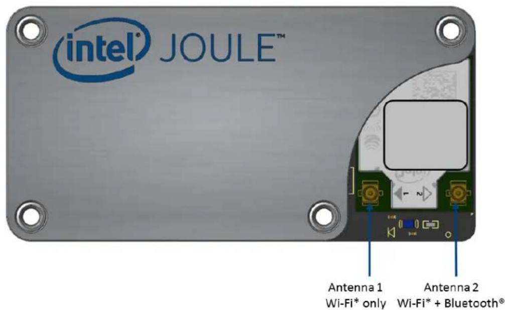
The module contains two MHF4 (U.FL compatible) antenna connectors that are labeled 1 and 2 with a triangle-shaped mark.
- A1 is dedicated to the Wi-Fi* service
- A2 supports both Wi-Fi* and Bluetooth® services
Figure 1 Wireless antenna connector location
5.5 The Intel ^® Dual Band Wireless-AC 8260 support site
Hyperlink: http://www.intel.com/content/www/us/en/support/network-and-i-o/wireless-networking/intel-wi-fi-products/intel-dual-band-wireless-ac-8000-series/intel-dual-band-wireless-ac-8260.html
Warning: En d-use equipment integrating the device has to be authorized as required by the U.S. Federal Communications Commission ("FCC") or it has to be operated in accordance with the FCC's rules on operation of unauthorized devices (47 C.F.R. § 2.805), including obtaining approval from any licensed spectrum operator, if the end-use equipment will use such operator's spectrum
Hyperlink: Regulatory Information for the Intel® Joule™ Compute Module
6 SD Card Interface
6.1 SD card interface features
· Host clock up to 208 MHz (SDR 104)
- Supports card detection (insertion/removal) with dedicated card detection signal
- Meets SD Host Controller Standard Specification version 3.0
• Meets SD Physical Layer Specification version 3.01
- Only supports SD memory
- Supports 1.8v signal levels directly; requires an external level shifter to support devices that operate above 1.8V
6.1.1 SD card signal group specifications
The Intel ^® Joule ^™ module provides a SD Card interface through the board-to-board connectors for expansion board usage. Refer to the Intel ^® Joule ^™ Compute Module Expansion Board Design Guide for the specifications and PCB routing guidance for this interface.
7 Module Connectors
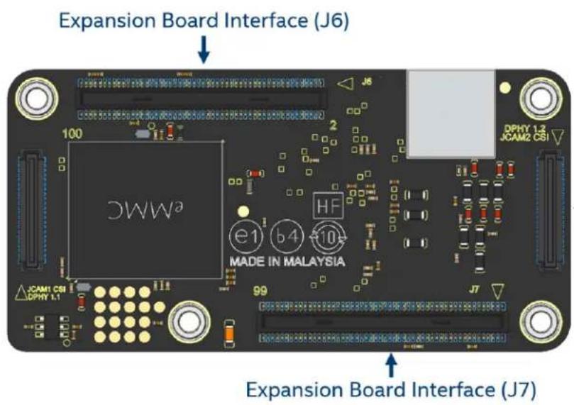
The Intel ^® Joule ^™ module utilizes two separate, connectors, (J6 & J7) to break out system buses, power and GPIO signals.
- All I/O signals are 1.8V with the exception of USB and PCIe which adhere to their respective standards.
- Module connectors J6 and J7 (2x50) are common with Hirose Electric Co LTD* Part Number DF40C-100DP-0.4V and mate with Hirose Electric Co LTD* Part Number DF40C-100DS-0.4V, or compatible.
· JCAM1 and JCAM2 are reserved for future development of MIPI base d imaging interfaces.
Figure 2 Module physical connectors
7.1 Module dimensions
See the Intel ^® Joule ^™ Platform Mechanical Descriptor for complete module and connector dimensions.
7.2 Module to expansion board connectors
7.2.1 Module electrostatic discharge
ESD testing is performed at the system level, where the module is connected to an expansion board, and not at the module connectors. See the Intel ^® Joule ^™ Compute Module Expansion Board Design Guide for more ESD information.
7.2.2 J6 connector interface signals
Table 8 J6 connector pin descriptions
| Pin Signal Name Usage Description | |||
| 36 +VDD1 | Output System 1.8 V | ||
| 30 +VDD3 | Output System 3.3 V | ||
| 41 | +V5P0V_VCONN | Input | Power for USB3.0 CC pins for VCONN-powered accessory. |
| 40 | CHRG_INT_N | Input | General purpose input/output for the expansion board charger's interrupt pin, active low.Allows charger to interrupt host to report charger device status and faults-connected to GPIO_19. |
| 35 | CHRG_EN_N | Output | General purpose input/output for the expansion board charger's enable pin, active low.Allows battery to be charged when power is connected to VDC_IN-connected to GPIO_15. |
| 43 | CODEC_MCLK | Output | MCLK for Master Mode operation for I2S audio |
| 16 | ISH_I2C_0_SCL | Output | Integrated sensor hub port 0 I2C clock (open collector) |
| 18 | ISH_I2C_0_SDA | Input/Output | Integrated sensor hub port 0 I2C data (open collector) |
| 21 | ISH_I2C_1_SCL | Output | Integrated sensor hub port 1 I2C clock (open collector) |
| 23 | ISH_I2C_1_SDA | Input/Output | Integrated sensor hub port 1 I2C data (open collector) |
| 46 | HDMI_CLK_DN | Output | HDMI* clock negative |
| 44 | HDMI_CLK_DP | Output | HDMI* clock positive |
| 68 | DDI1_CTRL_CLK | Output | HDMI* I2C clock |
| 70 | DDI1_CTRL_DAT | Input/Output | HDMI* I2C data |
| 62 | HDMI_TX_0_DN | Output | HDMI* data lane 0 negative |
| 58 | HDMI_TX_1_DN | Output | HDMI* data lane 1 negative |
| 50 | HDMI_TX_2_DN | Output | HDMI* data lane 2 negative |
| 64 | HDMI_TX_0_DP | Output | HDMI* data lane 0 positive |
| 56 | HDMI_TX_1_DP | Output | HDMI* data lane 1 positive |
| 52 | HDMI_TX_2_DP | Output | HDMI* data lane 2 positive |
| 74 | UART2_CTS | Input | UART port 2 clear to send. UART port 2 is used as a debug port for BIOS messages during boot. |
| 76 | UART2_RTS | Output | UART port 2 ready to send. UART port 2 is used as a debug port for BIOS messages during boot. |
| 80 | UART2_RXD | Input | UART port 2 receive data. UART port 2 is used as a debug port for BIOS messages during boot. |
| 78 | UART2_TXD | Output | UART port 2 transmit data. UART port 2 is used as a debug port for BIOS messages during boot. Pin includes hardware strapping functionality for DNX boot. |
| 4,10,19,42,48,54,60,66,72,73,82,86,96,98,100 | GND | Ground System ground | |
| 39 | I2S_1_CLK | Input/Output | I2S bit clock. Supplied by the module in master mode and serves as an input in slave mode. |
| 45 | I2S_1_FS | Output | I2S frame sync |
| 47 | I2S_1_RXD | Input | I2S receive data |
| 49 | I2S_1_TXD | Output | I2S transmit data |
| 94 | GPIO_22 | Input/Output | General purpose input/output |
| 1 | PWM_0 | Output | Programmable pulse width modulator port 0 |
| 3 | PWM_1 | Output | Programmable pulse width modulator port 1 |
Table 8 J6 connector pin descriptions
| Pin | Signal Name | Usage | Description |
| 22 | PWM_2 | Output | Programmable pulse width modulator port 2 |
| 24 | PWM_3 | Output | Programmable pulse width modulator port 3 |
| 65 | HPD_SRC | Input | General purpose input/output for HDMI cable hot plug detect. Instantiates a start-up communication between source and sink HDMI devices. Connected to GPIO_200. |
| 84 | BTN_N | Input | Connected to general purpose button on the expansion board. Connected to GPIO_17. |
| 57 I2C_0_SCL Output I | ^a C port 0 clock | ||
| 95 I2C_0_SDA Input/Output I | ^a C port 0 data | ||
| 25 | ISH_GPIO_0 | Input/Output | ISH general purpose input/output 0 |
| 27 | ISH_GPIO_1 | Input/Output | ISH general purpose input/output 1 |
| 32 | ISH_GPIO_2 | Input/Output | ISH general purpose input/output 2 |
| 34 | ISH_GPIO_3 | Input/Output | ISH general purpose input/output 3 |
| 29 | ISH_GPIO_4 | Input/Output | ISH general purpose input/output 4 |
| 38 | ISH_GPIO_5 | Input/Output | ISH general purpose input/output 5 |
| 31 | ISH_GPIO_6 | Input/Output | ISH general purpose input/output 6 |
| 71 CLK_19P2M Output 19.2 MHz clock | |||
| 69 | OTG_EN | Output | General purpose input/output controlled by PMIC to enable the module to power a USB OTG device |
| 9 | PMIC_PWRBTN_N | Input | System power/sleep button input to PMIC; active low. |
| 33 | PMIC_PWRGOOD | Output | Notification to system that all cold boot voltage rails to power the system have ramped up. Transitions high when module rails are within specification. |
| 13 | PMIC_RESET_N | Input | Notification to system that PMIC will respond to commands. When asserted, the PMIC will not respond to SoC commands via I2C or SVID because of the PMIC being either in standby or because a TLP is running. This is an active low signal. |
| 79 | SDCARD_CD_N | Input | SD card detect. Active low when a card is present, pulled high with internal pull-up when card is not present. |
| 75 | SDCARD_CLK | Output | SD card clock |
| 89 | SDCARD_CMD | Input/Output | SD card command is used for card initialization and transfer of commands. |
| 81 | SDCARD_D0 | Input/Output | SD card data 0. By default, during power up or reset, only data 0 is used for data transfer. |
| 83 | SDCARD_D1 | Input/Output | SD card data 1 |
| 85 | SDCARD_D2 | Input/Output | SD card data 2 |
| 87 | SDCARD_D3 | Input/Output | SD card data 3 |
| 77 | SDCARD_LVL_CLK_FB | Input | SD card clock feedback for aligning the SDIO data from the level shifter on-board the expansion board via the controller. There is a loopback through the SD card level shifter that drives this pin. |
| 90 | SDCARD_LVL_CMD_DIR | Output | SD card command direction indicates whether host is transmitting or receiving over the command pin. |
| 67 | SDCARD_LVL_DAT_DIR | Output | SD card data direction indicates whether host is transmitting or receiving over the data. |
| 88 | SDCARD_LVL_SEL | Output | SD card level select performs the 1.8V to 3.0V negotiation. |
| 91 SDCARD_PWR_DOWN_N | Output SD card power down indicates to SDIO device to power down. | ||
| 53 | SPI_1_CLK | Output | SPI port 1 clock |
| 63 | SPI_1_MISO | Input | SPI port 1 receive data |
| 55 | SPI_1_FS0 | Output | SPI port 1 slave select 0 |
| 14 | SPI_1_FS2 | Output | SPI port 1 slave select 2. Hardware strap with disable boot from SD card functionality. |
| 51 | SPI_1_MOSI | Output | SPI port 1 transmit data |
| 93 | UART_0_TXD | Output | UART port 0 transmit data. Hardware strap with reserved functionality. Note: Goes with UARTO signals on other connector |
| 26 | UART_1_RXD | Input | UART port 1 receive data |
| 28 | UART_1_TXD | Output | UART port 1 transmit data. Hardware strap with disable boot from eMMC functionality. |
| 20 | USB2_ID_PMIC | Input | USB OTG ID for device attach/detach and USB ACA detection via detection of resistance connected to pin. Connected to PMIC USBID pin. |
| 8 | USB2_0_DN | Input/Output | USB 2.0 port 0 data negative. Connected to PMIC USB 2.0 port 0. |
| 6 | USB2_0_DP | Input/Output | USB 2.0 port 0 data positive. Connected to PMIC USB 2.0 port 0. |
Table 8 J6 connector pin descriptions
| Pin | Signal Name | Usage | Description |
| 59 | USB_TYPE_CC1 | Input/Output | USB type-C configuration channel 1. Connected to PMIC CC channel 1 pin. |
| 61 | USB_TYPE_CC2 | Input/Output | USB type-C configuration channel 2. Connected to PMIC CC channel 2 pin. |
| 11 | +VRTC | Input | Real-time clock backup battery input to PMIC. |
| 92 | +VBATTERY | Input | Senses when battery is plugged in |
| 99 | +VBUS | Input | +VBUS from USB for PMIC detection when USB power source is plugged in. |
| 97 | VCONN_DCDC_EN | Output | General purpose input/output controlled by PMIC to enable load switch on expansion board to supply power to USB3.0 CC pins. |
| 37 | +VDC_IN | Input | +VDC_IN from DC jack for PMIC detection when DC jack is plugged in. |
| 2,5,7,12,15,17 | VSYS Input System power |
7.2.3 J7 connector interface signals
Table 9 J7 connector pin descriptions
| Pin Signal | Name Usage | Description | |
| 52 | AVS_M_CLK_A1 | Output | Microphone clock for channel A (voice trigger microphone) |
| 62 | AVS_M_CLK_B1 | Output | Microphone clock for channel B (secondary microphone) |
| 66 | AVS_M_DATA_1 | Input | First microphone pair data |
| 75 | FLASH_TORCH | Output | Output from shutter switch when it's pressed full way. This switch state is used to trigger Xenon flash or LED flash |
| 73 | FLASH_RST_N | Input | Output from shutter switch when it's pressed halfway. This switch state is used to trigger the Auto focus LED for Xenon Flash or Torch mode for LED flash, active low |
| 71 | FLASH_TRIGGER | Input | Control signal to Xenon Flash to start charging capacitor |
| 2,5,8,10,16,17,23,24,29,30,35,36,41,42,54,60,61,67,74,80,84,85,91,90,93,96,99 | GND | Ground | System ground |
| 43 | I2C_1_SCL | Output | I2C port 1 clock |
| 45 | I2C_1_SDA | Input/Output | I2C port 1 data |
| 9 | ISH_UART_0_CTS | Input | Integrated sensor hub UART port 0 clear to send |
| 11 | ISH_UART_0_RTS | Output | Integrated sensor hub UART port 0 return to send. Hardware strap with reserved functionality. |
| 13 | ISH_UART_0_RXD | Input | Integrated sensor hub UART port 0 receive data |
| 15 | ISH_UART_0_TXD | Output | Integrated sensor hub UART port 0 transmit data. Hardware strap with reserved functionality. |
| 26 | I2C_2_SDA | Input/Output | I2C port 2 data |
| 28 | I2C_2_SCL | Output | I2C port 2 clock |
| 12,14,38,40,69,81,83,92,94,98,100 | Reserved | Reserved | Do not use; leave disconnected |
| 88 | PCIE1_CLK_DN | Output | PCIe port 1 clock negative |
| 86 | PCIE1_CLK_DP | Output | PCIe1 port 1 clock positive |
| 50 | PCIE1_CLKREQ_N | Input | PCIe1 port 1 clock request, active low |
| 72 | PCIE1_WAKE_N | Input | PCIe1 wake, active low |
| 70 | PCIE1_PERST_n | Output | PCIe1 reset, active low |
Table 9 J7 connector pin descriptions
| Pin | Signal Name Usage | Description |
| 7 PMIC_SL | PCLK_1 Output 32kHz RTC | |
| 59 SPI_0_CLK | Output SPI port 0 clock | |
| 49 | SPI_0_MISO | Input SPI port 0 receive data |
| 77 | SPI_0_FS0 | Output SPI port 0 chip select 0. Hardware strap with reserved functionality. |
| 79 | SPI_0_FS1 | Output SPI port 0 chip select 1. Hardware strap with reserved functionality. |
| 53 | SPI_0_FS2 | Output SPI port 0 chip select 2 |
| 57 | SPI_0_MOSI | Output SPI port 0 transmit data |
| 47 | UART_0_CTS | Input UART port 0 clear to send |
| 55 | UART_0_RTS | Output UART port 0 return to send |
| 51 | UART_0_RXD | Input UART port 0 receive data (note UART_0_TXD is on the other 100p connector) |
| 18 | USBC_SEL | Output PMIC mux control for USB type-C polarity |
| 63 | USB2_1_DN | Input/Output USB 2.0 data negative |
| 65 | USB2_1_DP | Input/Output USB 2.0 data positive |
| 44 | USB3_0_RX_DN | Input USB 3.0 data receive negative |
| 46 | USB3_0_RX_DP | Input USB 3.0 data receive positive |
| 6 | USB3_0_TX_DN | Output USB 3.0 data transmit negative |
| 4 | USB3_0_TX_DP | Output USB 3.0 data transmit positive |
| 95 | USB3_1_RX_DP | Input USB 3.0 data receive negative |
| 97 | USB3_1_RX_DN | Input USB 3.0 data receive positive |
| 89 | USB3_1_TX_DN | Output USB 3.0 data transmit negative |
| 87 | USB3_1_TX_DP | Output USB 3.0 data transmit positive |
| 1,3,20,22,32,34 | VSYS | Input System power |
8 I2C Interfaces
The Intel ^® Joule ^™ module provides 7 master I2C interfaces.
8.1 I2C features
- ISH_I2C_0 and ISH_I2C_1 support standard, full and fast modes with a maximum data speed of 1.7Mbps
· I2C_0 through I2C_6 support standard, full, fast and high-speed modes with a maximum data speed of 3.4Mbps - I^2C master mode only; no support for multi-master mode
- Clock stretching by slave devices is possible
- Both 7-bit and 10-bit addressing modes are supported
8.2 I2C default configuration
Table 10 I2C mapping
| Name Description/Usage Source Destination | |||
| I2C_0 | Dedicated EEPROM on expansion board (holds configuration table) | LPSS | Routed on module J7 for expansion board use |
| I2C_1 | General usage | LPSS | Routed on module J7 for expansion board use |
| I2C_2 | General usage | LPSS | Routed on module J7 for expansion board use |
| I2C_3 | Camera support for DPHY 1.1 | LPSS | Module Camera Connector - JCAM2 |
| I2C_4 | Camera support for DPHY 1.2 & 1.1 | LPSS | Module Camera Connector - JCAM1 |
| ISH_I2C_0 | General usage; mapped to LPSS I2C_5 | LPSS | Routed on module J6 for expansion board use |
| ISH_I2C_1 | General usage; mapped to LPSS I2C_6 | LPSS | Routed on module J6 for expansion board use |
8.3 I2C signal group specifications
Refer to the Intel® Joule™ Compute Module Expansion Board Design Guide for the specifications and PCB routing guidance for this interface.
9 Clock Specifications
Two module clocks, 19.2 MHz (CLK_19P2M) and 32.768 kHz (PMIC_SLPCLK_1) are routed out through the board-to-board connectors for use on expansion boards.
Refer to the Intel® Joule™ Compute Module Expansion Board Design Guide for the specifications and PCB routing guidance of the clocks.
9.1 RTC backup battery
A backup power source is required for the RTC to operate robustly by preventing RTC data losses during unexpected power events. Implementation options are provided in the Intel® Joule™ Compute Module Expansion Board Design Guide (listed in Section 1.2).
The most common solution is a non-rechargeable coin-cell battery connected to V_RTC at module connector J6, pin 11.
10 UART Specifications
10.1 UART availability
Table 11 Available UARTS
| Name Type Flow Control | ||
| UART0 | Full HSUART support - dedicated to Boot Mode strapping on expansion board | Yes |
| UART1 Receive / Transmit only None | ||
| UART2 Full HSUART support Yes | ||
| ISH UART 0 Full HSUART support Yes |
Refer to the Intel® Joule™ Compute Module Expansion Board Design Guide for the specifications and PCB routing guidance for these interfaces.
11 I2S Specifications
One I2S port is provided by the J7 board-to-board connector interface.
11.1 I2S signal group specifications
Refer to the Intel ^® Joule ^™ Compute Module Expansion Board Design Guide for the specifications and PCB routing guidance for this interface.
11.1.1 I2S available formats
The I2S formats listed in Table 12 have not been verified and are subject to change.
Table 12 I2S available configuration formats
| Mode Priority Frame | rate | Bits/sample | Number of slots | Frame to data offset | Frame polarity | Frame width | Frame rate inaccuracy | Notes | |
| I^2S master | 1 192K,96 | K,48K, 16K,8K | 16,24 2 1 | 0-left | 1-right | 50/50 | 0% Standard I | ^2S protocol. 50% duty | |
| PCM slave-SFS | 1 192K,96 | K,48K, 44.1K, 16K, 8K | 16,24 | 192kHz: 296 kHz: 4All else: 1 to 6 | 0 | High | |||
| PCM slave - LFS | 1 192K, | 96K, 48K,44.1K,16K,8K | 16,24 | 192 kHz: 296 kHz: 4 All else: 1 to 6 | 0 | High | 0%. | ||
| PCM master -SFS | 1 192K, | 96K, 48K,16K, 8K | 16, 24 192 | kHz: 2All else: 1 to 4 | 0 | High | 1 bit clock wide | 0% Rising edge | frame sensitive.Design supports more frame- to-data offset options. |
| PCM master - LFS | 1 192K, | 96K, 48K,16K, 8K | 16,24 | 192 kHz: 2All else: 1 to 4 | 0 | High | 1-bit to n-bit clocks | 0% Design supports width > 1 slot. | |
| Left justified master | 2 192K,96 | K,48K | 16,24 | 2 | 0 | 0-left, 1-right | 50/50 | 0% | Design supports flipping polarity on the frame signal. |
| I^2S slave | 3 | 192K,96K,48K,44.1K | 16,24 | 2 | 0 | 0-left, 1-right | 50/50 | 0% | |
| Left justified slave | 3 | 192K,96K,48K | 16,24 | 2 | 0 | 0-left, 1-right | 50/50 | 0% | |
| Right justified | Not supported. | ||||||||
11.2 Digital microphone ports
The Intel ^® Joule ^™ module supports microphones that use the PDM digital microphone standard and attached to the module through the AVS_M interface. Two microphones can share one data line by using time domain multiplexing to the two slots.
PDM microphones are enabled and disabled by the clock signal. Absence of clock signal will switch microphone to sleep mode, which can be utilized in system power management.
Additionally the microphones can be power-gated to cut the power consumption to zero when microphones are not used.
Refer to the Intel ^® Joule ^™ Compute Module Expansion Board Design Guide for the specifications and PCB routing guidance for this interface.
12 GPIO Specifications
12.1 Dedicated GPIO lines
The Intel ^® Joule ^™ module provides 8 dedicated GPIO lines (GPIO_0 - 6, GPIO_17 and GPIO_22) connected to the core processor.
12.2 Reconfigurable interfaces buses as GPIO
Many interface lines on the module can be reconfigured as GPIO lines by defining a configuration table stored within an EEPROM device on the expansion board.
The BIOS loads a default configuration (see BIOS release notes for more details) if the EEPROM appears empty or is found unreadable by the BIOS. The configuration EEPROM is only read at cold boot and the configuration is retained during reset. Specific outputs can be set or cleared before entering a sleep state.
12.3 GPIO internal pull UP / pull DOWN resistors
Each GPIO line can employ an internal pull UP or pull DOWN resistor, this is also defined within the configuration table and stored in the expansion board EEPROM device and read by the BIOS at cold boot.
See the TBD-Intel® Joule™ BIOS Guide for pull UP and pull DOWN configuration details and the Intel® Joule™ Compute Module Expansion Board Design Guide for the specifications and PCB routing guidance of the GPIO interfaces.
12.4 Operating System GPIO to function mapping
GPIO signals are configured in BIOS for each supported operating system. The default mapping can change with each iteration of the BIOS. Refer to the Intel Joule compute module website for the current default mapping for each supported operating system.
13 Pulse Width Modulators
The default BIOS configuration table defines four dedicated PWM outputs as PWM_0, PWM_1, PWM_2, and PWM_3, each with programmable frequency and duty cycle.
Table 13 shows examples of hardware (register) based PWM programming:
The PWM variables that control frequency and duty cycle are controlled by the BASE_UNIT_INT, BASE_UNIT_FRAC, and ON_TIME_DIVISOR register settings and the following equations:
13.1 PWM frequency formula:
$$ \text { Frequency } \approx 1 9. 2 \mathrm{MHz} * \frac {\left(\text { PWM BASE UNIT }\right) _ {d}}{2 5 6} $$
13.2 PWM duty cycle formula:
$$ \text { Duty Cycle } \approx \frac {\left(\text { PWM ON TIME DIVISOR }\right) _ {d}}{2 5 6} $$
Note: Consult specific operating system documents if manipulating PWM settings at the OS level.
Table 13 PWM programming examples
| Integer part of BASE_UNIT_INT (bits 29:22) | Fractional part of BASE_UNIT_FRAC (bits 21:8) | Decimal base unit value | ON_TIME_DIVISOR (bits 7:0) | Base unit type | PWM frequency (Hz) | PWM period (uSec) | Duty Cycle |
| 0000_0000b | 00_0100_0000_0000b | 0.0625 | 0000_1000b | fractional | 4,688 | 213 | 50% |
| 0000_0000b | 00_0010_0000_0000b | 0.03125 | 0000_0100b | fractional | 2,344 | 427 | 50% |
| 0000_0000b | 00_0001_0000_0000b | 0.015625 | 0000_0001b | fractional | 1,172 | 853 | 50% |
14 Universal Serial Bus
14.1 Available USB ports
The Intel ^® Joule ^™ module provides two USB 3.0 ports; one Type C (OTG) and one USB 3.0 host mode and a USB 2 host port.
Table 14 USB port types
| Signal name Port Description | ||
| USB2_0_DP | 0 | USB 2 data positive |
| USB2_0_DN | USB 2 data negative | |
| USB3_1_RX_DP | 1 | USB 3 receive data positive |
| USB3_1_RX_DN | USB 3 receive data negative | |
| USB3_1_TX_DP | USB 3 transmit data positive | |
| USB3_1_TX_DN | USB 3 transmit data negative | |
Refer to the Intel ^® Joule ^™ Compute Module Expansion Board Design Guide for the specifications and PCB routing guidance for this interface.
- Revision History
- Contents
- Clock Specifications....22
- UART Specifications....23
- I2S Specifications 23
- GPIO Specifications....24
- Pulse Width Modulators 24
- Universal Serial Bus 25
- Tables
- Figures
- Introduction
- Acronyms
- Reference documents
- System on Module Overview
- Intel ® Joule ™ module configurations
- Intel ® Joule ™ compute module feature summary
- Expansion board requirements
- Method for connecting module to expansion board
- Method to provide +VSYS power to the module
- Required strapping of module pins
- BIOS installed onto module
- Expansion board recommendations
- External EEPROM for multipurpose pin configuration data
- Power button
- DnX button
- Real time clock (RTC) backup power source
- UART debugging
- Power Delivery, Signaling, and Reset
- Main power supply (VSYS)
- Power on signaling
- +VDC\_IN power sensing
- +VBUS power sensing
- Power good
- Hard shutdown via power button
- System voltage rail specifications
- Graphics Specifications
- Intel ® Gen9LP features
- Graphic encoder and decoder support
- HDMI\* signal group specifications
- Wireless Connectivity
- Intel® Dual Band Wireless-AC 8260 highlights
- Wi-Fi features
- Bluetooth ® highlights
- Supported Bluetooth® profiles
- Security
- Wireless antenna connectors
- The Intel ® Dual Band Wireless-AC 8260 support site
- SD Card Interface
- SD card interface features
- SD card signal group specifications
- Module Connectors
- Module dimensions
- Module to expansion board connectors
- Module electrostatic discharge
- J6 connector interface signals
- J7 connector interface signals
- I2C Interfaces
- I2C features
- I2C default configuration
- I2C signal group specifications
- Clock Specifications
- RTC backup battery
- UART Specifications
- UART availability
- I2S Specifications
- I2S signal group specifications
- I2S available formats
- Digital microphone ports
- GPIO Specifications
- Dedicated GPIO lines
- Reconfigurable interfaces buses as GPIO
- GPIO internal pull UP / pull DOWN resistors
- Operating System GPIO to function mapping
- Pulse Width Modulators
- PWM frequency formula:
- PWM duty cycle formula:
- Universal Serial Bus
- Available USB ports
Brand : INTEL
Model : Joule 550x Compute Module
Category : Computer module