
X18-M SATA II - SSD INTEL - Free user manual and instructions
Find the device manual for free X18-M SATA II INTEL in PDF.


| Product Type | Solid State Drive (SSD) |
| Brand | Intel |
| Model | X18-M SATA II |
| Interface | SATA II (3 Gbps) |
| Form Factor | 1.8-inch |
| Capacity | 80 GB (also available in 160 GB) |
| NAND Flash Type | Multi-Level Cell (MLC) |
| Sequential Read Speed | Up to 250 MB/s |
| Sequential Write Speed | Up to 70 MB/s |
| Power Consumption (Active) | 0.15 W typical |
| Power Consumption (Idle) | 0.06 W typical |
| Dimensions (W x H x D) | 54 x 78.5 x 5 mm |
| Weight | 20 g |
| Operating Temperature | 0 to 70 °C |
| Storage Temperature | -40 to 85 °C |
| Shock Resistance | 1500 G / 0.5 ms |
| MTBF | 1.2 million hours |
| Warranty | 3 years (limited) |
| Supported Features | TRIM, S.M.A.R.T., NCQ |
| Installation Notes | May require 2.5-inch adapter for standard bays |
| Cleaning | Use dry soft cloth; avoid liquids |
| Safety Precautions | ESD sensitive; handle by edges, ground yourself |
| Spare Parts / Repairability | Not user-serviceable; sealed unit |
Frequently Asked Questions - X18-M SATA II INTEL
User questions about X18-M SATA II INTEL
0 question about this device. Answer the ones you know or ask your own.
Ask a new question about this device
Download the instructions for your SSD in PDF format for free! Find your manual X18-M SATA II - INTEL and take your electronic device back in hand. On this page are published all the documents necessary for the use of your device. X18-M SATA II by INTEL.
USER MANUAL X18-M SATA II INTEL
Intel® X25-E SATA Solid State Drive
SSDSA2SH032G1, SSDSA2SH064G1
Product Manual
■ Available in 2.5" Form Factor
■ Capacity: 32 GB, 64 GB
■ Uses Intel NAND flash memory Single Level Cell (SLC) components
■ Bandwidth Performance Specifications
— Sustained Sequential Read: up to 250 MB/s
— Sustained Sequential Write: up to 170 MB/s
- Read and Write IOPS Specifications (IOmeter Queue Depth 32)
— Random 4 KB Reads: 35 K IOPS
— Random 4 KB Writes: 3.3 K IOPS
- Compatibility — In t® Matrix Storage Manager — SATA Revision 2.6 compliant, compatible with SATA 1.5 Gb/s and 3 Gb/s interface rates — ATA/ATAPI-7 Compliant — SSD Enhanced SMART ATA feature set — Native Command Queuing (NCQ) command
■ Compliance — UL* — CE* — C - Tick * — B S M I * — M I C * — M i c r o s o f t * W H Q L — R o H S *
Power Management
— 5 V SATA Supply Rail
— Supports ATA Power Management and Advanced Power Management Specifications
— SATA Interface Power Management
— OS-Aware Hot Plug/Removal
■ Power Specifications — Active: 2.4/2.6 W (32 GB/64 GB) TYP — Idle: .060 W TYP
■ Temperature — Operating: -55^ C to 95^ C — Non-Operating: -55^ C to 95^ C
- Reliability — Bit Error Rate (BER): 1 sector per 10^15 bits read — Mean Time Between Failures (MTBF) 2,000,000 Hours — Write Endurance: 1 petabyte of random writes
■ Shock — Operating and Non-operating: 1,000G/0.5 msec
■ Vibration — Operating: 2.17 G (7-800 Hz) — Non-operating 3.13 G (10-500 Hz)
■ Weight: — 80 +/- 2 grams (32 GB) — 90 +/- 2 grams (64 GB) (2.5" 7 mm Form Factors)
Ordering Information
Decoder
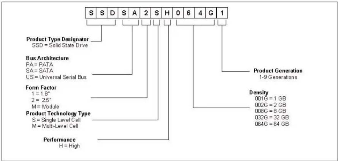
flowchart
graph TD
    A["Product Type Designator\nSSD = Solid State Drive"] --> B["Bus Architecture\nPA = PATA\nSA = SATA\nUS = Universal Serial Bus"]
    B --> C["Form Factor\n1 = 1.8"\n2 = 2.5"\nM = Module"]
    C --> D["Product Technology Type\nS = Single Level Cell\nM = Multi-Level Cell"]
    D --> E["Performance\nH = High"]
    F["Product Generation\n1-9 Generations"] --> G["Density\n001G = 1 GB\n002G = 2 GB\n008G = 8 GB\n032G = 32 GB\n064G = 64 GB"]
Intel High Performance Solid State Drive Ordering Information
| Part Number MM | # Device Nom | enclature Packaging | |
| SSDSA2SH032G101 | 896432 32 GB | SATA 2.5" Drive SLC High Performance, Production Sample 1 unit | |
| SSDSA2SH032G1C5 | 900342 32 GB | SATA 2.5" Drive SLC High Performance, Production Sample 5 unit | |
| SSDSA2SH032G1 | 896474 32 GB | SATA 2.5" Drive SLC High Performance, Production Sample 50 unit | |
| SSDSA2SH064G101 | 899386 64 GB | SATA 2.5" Drive SLC High Performance, Production Sample 1 unit | |
| SSDSA2SH064G1C5 | 901316 | 64 GB SATA 2.5" Drive SLC High Performance, Production Sample | 5 units |
| SSDSA2SH064G1 | 899387 | 64 GB SATA 2.5" Drive SLC High Performance, Production Sample | 50 units |
INFORMATION IN THIS DOCUMENT IS PROVIDED IN CONNECTION WITH INTEL® PRODUCTS. NO LICENSE, EXPRESS OR IMPLIED, BY ESTOPPEL OR OTHERWISE, TO ANY INTELLECTUAL PROPERTY RIGHTS IS GRANTED BY THIS DOCUMENT. EXCEPT AS PROVIDED IN INTEL'S TERMS AND CONDITIONS OF SALE FOR SUCH PRODUCTS, INTEL ASSUMES NO LIABILITY WHATSOEVER, AND INTEL DISCLAIMS ANY EXPRESS OR IMPLIED WARRANTY, RELATING TO SALE AND/OR USE OF INTEL PRODUCTS INCLUDING LIABILITY OR WARRANTIES RELATING TO FITNESS FOR A PARTICULAR PURPOSE, MERCHANTABILITY, OR INFRINGEMENT OF ANY PATENT. COPYRIGHT OR OTHER INTELLECTUAL PROPERTY RIGHT. Intel products are not intended for use in medical, life saving, life sustaining, critical control or safety systems, or in nuclear facility applications.
Intel may make changes to specifications and product descriptions at any time, without notice.
Intel Corporation may have patents or pending patent applications, trademarks, copyrights, or other intellectual property rights that relate to the presented subject matter. The furnishing of documents and other materials and information does not provide any license, express or implied, by estoppel or otherwise, to any such patents, trademarks, copyrights, or other intellectual property rights.
Designers must not rely on the absence or characteristics of any features or instructions marked "reserved" or "undefined." Intel reserves these for future definition and shall have no responsibility whatsoever for conflicts or incompatibilities arising from future changes to them.
Except as permitted by such license, no part of this document may be reproduced, stored in a retrieval system, or transmitted in any form or by any means without the express written consent of Intel Corporation.
Contact your local Intel sales office or your distributor to obtain the latest specifications and before placing your product order. Copies of documents which have an order number and are referenced in this document, or other Intel literature may be obtained by calling 1-800-548-4725 or by visiting Intel's website at http://www.intel.com.
Intel and Intel logo are trademarks or registered trademarks of Intel Corporation or its subsidiaries in the United States and other countries.
* Other names and brands may be claimed as the property of others. Copyright © 2009, Intel Corporation. All Rights Reserved.
Contents
1.0 Introduction....5
1.1 Product Overview ....5
1.2 Block Diagram 6
1.3 Architecture....6
2.0 Certifications and Compliance 7
3.0 Product Specifications 7
3.1 Capacity 7
3.2 Performance....7
3.3 Electrical Characteristics....8
3.3.1 Supply Voltage....8
3.3.2 Power Consumption....8
3.4 Environmental Conditions....9
3.4.1 Temperature....9
3.4.2 Altitude....9
3.4.3 Shock and Vibration....9
3.4.4 Acoustics 10
3.4.5 Electromagnetic Immunity.... 10
3.5 Reliability 10
3.5.1 Non-recoverable read errors 11
3.5.2 Mean Time Between Failure 11
3.5.3 Power On/Off Cycles.... 11
3.5.4 Write Endurance 11
4.0 Mechanical Information....12
5.0 Pin and Signal Descriptions 13
5.1 Pin Locations 13
5.2 Signal Description Table.... 13
5.3 Hot Plug Support.... 14
6.0 Command Sets 15
6.1 ATA Commands 15
6.1.1 ATA General Feature Command Set 15
6.1.2 Power Management Command Set.... 18
6.1.3 Security Mode Feature Set.... 18
6.1.4 SMART Command Set 19
6.1.5 Host Protected Area Command Set 19
6.1.6 48-Bit Address Command Set 19
6.1.7 Device Configuration Overlay Command Set 19
6.1.8 General Purpose Log Command Set 20
6.2 SATA Commands.... 20
6.2.1 Software Settings Preservation.... 20
6.2.2 Native Command Queuing 20
7.0 References 21
8.0 Glossary 22
9.0 Revision History 23
1.0 Introduction
The Intel ^® X25-E SATA Solid State Drive (SSD) delivers ultimate performance in an industry standard 2.5" form factor while simultaneously improving system responsiveness over standard rotating media or hard disk drives (HDD) in some of the most demanding applications. By combining Intel's leading NAND flash memory technology with our innovative controller, Intel delivers an SSD for Native Serial Advanced Technology Attachment (SATA) hard disk drive drop-in replacement with enhanced performance, reliability, ruggedness and power savings.
Since there are no rotating platters, moving heads, fragile actuators, unnecessary spin-up time or positional seek time that can significantly slow down the storage subsystem, the Intel X25-E SATA SSD enables fast read/write access times and significant I/O, as well as performance improvement when compared to rotating media.
This document describes the specifications of the Intel X25-E SATA SSD in the 2.5" form factor.
1.1 Product Overview
The Intel X25-E SATA SSD primarily targets high-end workstations, desktops, gaming and various server/storage applications. Key attributes include extremely high performance, low power, enhanced reliability and improved ruggedness as compared to standard 10,000 and 15,000 RPM SATA hard drives. The Intel X25-E SATA SSD is available in an industry standard 2.5" form factor that is electronically, mechanically, and software compatible with existing SATA and Serial Attached SCSI (SAS) slots and cables.
1.2 Block Diagram
Figure 1. Block Diagram
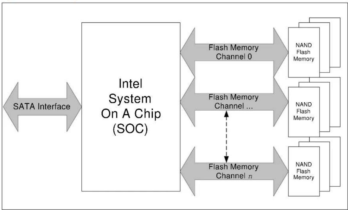
flowchart
graph LR
    A["SATA Interface"] --> B["Intel System On A Chip (SOC)"]
    B --> C["Flash Memory Channel 0"]
    B --> D["Flash Memory Channel ..."]
    B --> E["Flash Memory Channel n"]
    C <--> F["NAND Flash Memory"]
    D <--> G["NAND Flash Memory"]
    E <--> H["NAND Flash Memory"]
    F --> I["Output"]
    G --> I
    H --> I
1.3 Architecture
The Intel ^® X25-E SATA Solid State Drives utilize a cost effective System on a Chip (SOC) design to manage a full SATA 3 Gb/s bandwidth with the host while managing multiple flash memory devices on multiple channels internally.
2.0 Certifications and Compliance
Table 1. Device Certifications
| Certification/ Compliance Description | |
| CE Compliant | Indicate conformity with the essential health and safety requirements set out in European Directives Low Voltage Directive and EMC directive. |
| UL Certified Underwriters Laboratories | , Inc. Component Recognition UL60950-1. |
| C-Tick Compliant | Compliance with EN 55022:2006 and the Electromagnetic Compatibility (EMC) Framework requirements of the Australian Communication Authority (ACA). |
| BSMI Compliant | Compliance to the Taiwan EMC standard "Limits and methods of measurement of radio disturbance characteristics of information technology equipment, CNS 13438 Class B." |
| MIC Certified | Compliance with paragraph 1 of Article 11 of the Electromagnetic Compatibility control Regulation and meet the Electromagnetic Compatibility (EMC) Framework requirements of the Radio Research Laboratory (RRL) Ministry of Information and Communication Republic of Korea. |
| Microsoft WHQL Certified Microsoft Windows Hardware Quality Labs | |
| RoHS Compliant Restriction of Hazardous Substance Directive | |
3.0 Product Specifications
3.1 Capacity
Table 2. User Addressable Sectors
| Unformatted Capacity Total User Addressable Sectors in LBA Mode | |
| 32 GB 62,500,000 | |
| 64 GB 125,045,424 | |
Notes:
- 1 GB = 1,000,000,000 Byte and not all of the memory can be used for data storage.
2.1 Sector = 512 Byte.
3.2 Performance
Table 3. Maximum Sustained Read and Write Bandwidth
| Access Type | MB/ s |
| Sequential Read | up to 250 |
| Sequential Write | up to 170 |
Notes:
-
Performance measured using lOmeter with queue depth set to 32.
-
Write Cache enabled.
Table 4. Random Read and Write Input/ Output Operations per Second (IOPS)
| Access Type IOPS | |
| 4K Read 35,000 | |
| 4K Write 3,300 |
Notes:
- Performance measured using IOMeter with queue depth set to 32.
- Write Cache enabled.
- Random IOPS cover the entire range of legal logical block addresses (LBAs). Measurements are performed on a full drive (all LBAs have valid content).
Table 5. Latency Specifications
| Type Average Latency | |
| Read 75 μs (TYP) | |
| Write 85 μs (TYP) | |
| Power On to Ready 1 s |
Notes:
- Write Cache enabled.
- Device measured using Iometer*
- Power On to Ready (POR) time assumes proper shutdown (power removal preceded by STANDBY command).
- Read/Write latency measured on 4 k transfers.
- Queue depth set to 1
- Sequential IOPS cover the entire range of legal logical block addresses (LBAs). Measurements are performed on a full drive (all LBAs have valid content).
3.3 Electrical Characteristics
3.3.1 Supply Voltage
Table 6. Operating Voltage
| Description Min | Max | Unit | ||
| Operating Voltage for 5 V (+/- 5%) | 4.75 | 5.25 | V | |
3.3.2 Power Consumption
Table 7. Typical Power Consumption
| Mode | Typ | Unit |
| Active | 2.4(32 GB)2.6(64 GB) | W |
| Idle | 0.06 | W |
Drive will transition to idle power level once idle for 25 ms whether or not sleep or standby command is received. Standby power levels assume DIPM enabled. Active power is measured on an IOMeter workload of full bandwidth 64 K sequential writes with queue depth 1.
3.4 Environmental Conditions
3.4.1 Temperature
Table 8. Temperature Related Specifications
| Mode Min Typ Max Unit | |||||
| Ambient Temperature | Operating 0 70 | °C | |||
| Non-Operating | -55 | 95 | °C | ||
| Temperature Gradient | Operating | 20 | °C/hr * | ||
| Non-Operating | 30 | °C/hr * | |||
| Humidity | Operating 5 95 | % | |||
| Non-Operating | 5 95 | % | |||
Note: Measured without condensation.
3.4.2 Altitude
The drive is not sensitive to changes in altitude because it has no moving parts. Drive tested between -1K and 40K feet.
3.4.3 Shock and Vibration
Table 9. Shock and Vibration Specifications
| Mode | Timing | Max | Unit | |
| Shock ^1 | Operating | at 0.5 msec | 1,000 G | |
| Non-Operating | at 0.5 msec | 1,000 G | ||
| Vibration ^2 | Operating | 2.17 G | 7-800 Hz | |
| Non-Operating | 3.13 G | 10-500 Hz ^3 |
Notes:
-
Shock specifications assumes that the SSD is mounted securely with the input vibration applied to the drive mounting screws. Stimulus may be applied in the X, Y or Z axis.
-
Vibration specifications assumes that the SSD is mounted securely with the input vibration applied to the drive mounting screws. Stimulus may be applied in the X, Y or Z axis.
-
Sine wave sweeping 1 oct/min.
3.4.4 Acoustics
The drive has no moving or noise-emitting parts; therefore, it produces negligible sound (0 dB) in all modes of operation.
3.4.5 Electromagnetic Immunity
Electromagnetic Immunity tests assume the SSD is properly installed in the representative host system. The drive will operate properly without errors or degradation in performance when subjected to radio frequency (RF) environments defined in the following table:
Table 10. Electromagnetic Immunity Specifications
| Test Description | Performance Criteria | Reference Standard | |
| Electrostatic discharge Contact, HCP, VCP: ±8 kV; Air: ±15 kV B EN 61000-4-2: 1995 | |||
| Radiated RF immunity | 80 to 1,000 MHz, 3 V/m,80% AM with 1 kHz sine900 MHz, 3 V/m, 50% pulse modulation at 200 Hz | A | EN 61000-4-3: 1996ENV 50204: 1995 |
| Electrical fast transient | ±1 kV on AC mains, ±0.5 kV on external I/O | B EN 61000-4-4: 1995 | |
| Surge immunity | ±1 kV differential, ±2 kV common, AC mains | B EN 61000-4-5: 1995 | |
| Conducted RF immunity | 150 kHz to 80 MHz, 3 Vrms, 80% AM with 1 kHz sine | A EN 61000-4-6: 1996 | |
| Voltage dips, interrupts | 0% open, 5 seconds0% short, 5 seconds40%, 0.10 seconds70%, 0.01 seconds | CCCB | EN 61000-4-11: 1994 |
Notes:
-
Performance Criteria A = The device shall continue to operate as intended, i.e., normal unit operation with no degradation of performance.
-
Performance Criteria B = The device shall continue to operate as intended after completion of the test. However, during the test, some degradation of performance is allowed as long as there is no data loss operator intervention to restore device function.
-
Performance Criteria C = temporary loss of function is allowed. Operator intervention is acceptable to restore device function.
-
Electrostatic Discharge applied to drive enclosure.
3.5 Reliability
Table 11. Reliability Specifications
| Parameter Value | |
| Nonrecoverable read errors (BER) 1 sector in 10 | ^15 bits read, max |
| Mean Time Between Failures (MTBF) 2,000,000 hours | |
| Power On/Off Cycles 50,000 cycles |
3.5.1 Non-recoverable read errors
The nonrecoverable read error rate will not exceed one sector in the specified number of bits read. In the extremely unlikely event of a nonrecoverable read error, the drive will report it as a read failure to the host; the sector in error is considered corrupt and is not returned to the host.
3.5.2 Mean Time Between Failure
The Mean Time Between Failures (MTBF) is calculated based on a Part Stress Analysis. It assumes nominal voltage, with all other parameters within specified range.
3.5.3 Power On/ Off Cycles
Defined as power being removed from the drive, and then restored. Note that host systems and drive enclosures may remove power from the drive for reasons other than a system shutdown.
3.5.4 Write Endurance
The drive supports 1 petabyte of lifetime random writes.
4.0 Mechanical Information
Figure 2. Dimensions
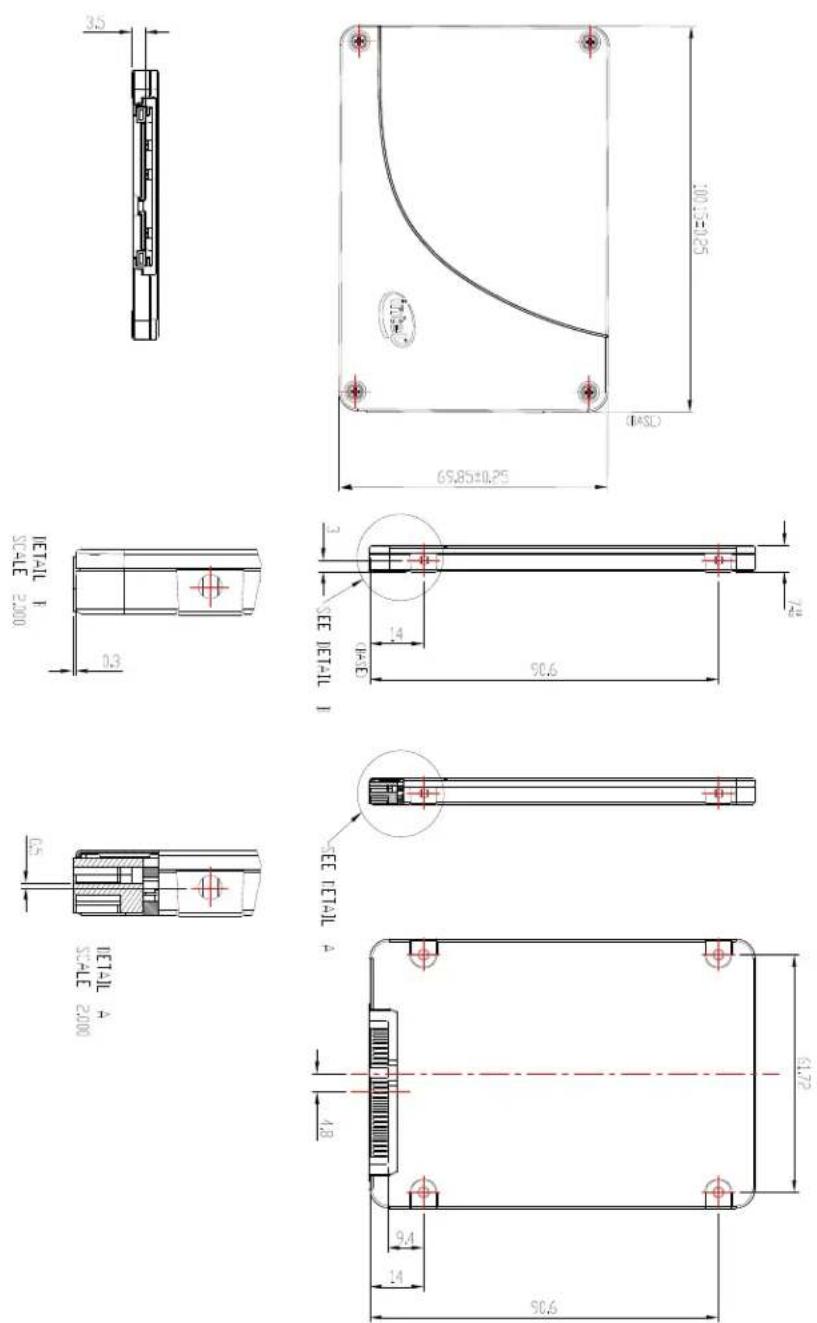
DETAIL A SCALE 2.000
Note: All dimensions are in millimeters.
5.0 Pin and Signal Descriptions
This section identifies the pin locations and signal descriptions of the Intel High Performance SSDs.
5.1 Pin Locations
Figure 3. Layout of Signal and Power Segment Pins
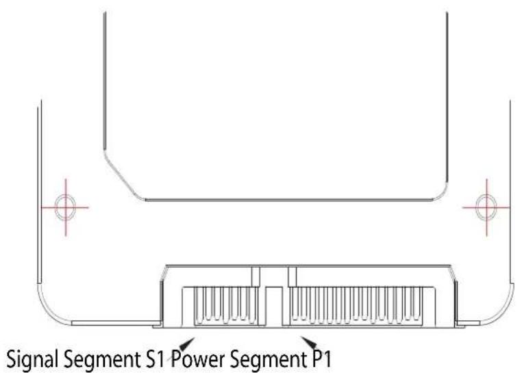
5.2 Signal Description Table
Table 12. Serial ATA Connector Pin Signal Definitions
| Pin Function Definition | ||
| S1 Ground 2nd mate | ||
| S2 A+ | Differential signal pair A | |
| S3 A- | ||
| S4 Ground 2nd mate | ||
| S5 B- | Differential signal pair B | |
| S6 B+ | ||
| S7 Ground 2nd mate | ||
Note: Key and spacing separate signal and power segments.
Table 13. Serial ATA Power Pin Definitions
| Pin^1 | Function Definition | Mating Order | |
| P1 Not connected. | 2 | 3.3 V Power 2nd Mate | |
| P2 Not connected | 2. | 3.3 V Power 2nd Mate | |
| P3 Not connected. | 2 | 3.3 V Power 1st Mate | |
| P4 Ground | 3, 4 | 1st Mate | |
| P5 Ground | 3 | 1st Mate | |
| P6 Ground | 3 | 1st Mate | |
| P7 | V_5^3,5 | 5 V Power 1st Mate | |
| P8 | V_5^3,5 | 5 V Power | 2nd Mate |
| P9 | V_5^3,5 | 5 V Power | 2nd Mate |
| P10 | Ground3 | 1st Mate | |
| P11 | DAS^6 | Device Activity Signal^6 | 2nd Mate |
| P12 | Ground3, 4 | 1st Mate | |
| P13 | Not connected.7 | 12 V Power | 2nd Mate |
| P14 | Not connected.7 | 12 V Power | 2nd Mate |
| P15 | Not connected.7 | 12 V Power | 2nd Mate |
Notes:
-
All pins are in a single row, with a 1.27 mm (0.050") pitch.
-
Pins P1, P2 and P3 are connected together, although they are not connected internally to the device. The host may put 3.3 V on these pins.
-
The mating sequence is:
- the ground pins P4-P6, P10, P12 and the 5v power pin P7.
- the signal pins and the rest of the 5V power pins P8-P9.
-
Ground connectors P4 and P12 may contact before the other 1st mate pins in both the power and signal connectors to discharge ESD in a suitably configured backplane connector.
-
Power pins P7, P8, and P9 are internally connected to one another within the device.
-
The host may ground P11 if it is not used for Device Activity Signal (DAS)
-
Pins P13, P14 and P15 are connected together, although they are not connected internally to the device. The host may put 12 V on these pins.
5.3 Hot Plug Support
Hot Plug insertion and removal are supported in the presence of a proper connector and appropriate operating system (OS) support as described in the SATA 2.6 specification. This product supports Asynchronous Signal Recovery and will issue an unsolicited COMINIT when first mated with a powered connector to guarantee reliable detection by a host system without hardware device detection.
6.0 Command Sets
6.1 ATA Commands
The Intel X25-E SATA SSD supports all the mandatory ATA commands defined in the ATA/ATAPI-7 specification.
6.1.1 ATA General Feature Command Set
The Intel X25-E SATA SSD supports the ATA General Feature command set (non-PACKET), which consists of
• EXECUTE DEVICE DIAGNOSTIC
- FLUSH CACHE
• IDENTIFY DEVICE
- READ DMA
- READ SECTOR (S)
- READ VERIFY SECTOR (S)
- SEEK
- SET FEATURES
• WRITEDMA
• WRITE SECTOR (S)
- READ MULTIPLE
- SET MULTIPLE MODE
- WRITE MULTIPLE
The Intel X25-E SATA SSD also supports the following optional commands:
- READ BUFFER
- WRITE BUFFER
• NOP - DOWNLOAD MICROCODE
6.1.1.1 IDENTIFY DEVICE Data
The following table details the sector data returned after issuing an IDENTIFY DEVICE command.
Table 14. Returned Sector Data
| Word | F = FixedV = VariableX = Both | Default Value Description | |
| 0 | F | 0040h | General configuration bit-significant information |
| 1 | X | 3FFFh | Obsolete - Number of logical cylinders (16,383) |
| 2 | V | C837h | Specific configuration |
| Word | F = FixedV = VariableX = Both | Default Value | Description |
| 3 X 00 | 0h Obsolete - Number of logical heads | (16) | |
| 4-5 X 0h | Retired | ||
| 6 X 003Fh | Obsolete - Number of logical sectors per logical track (63) | ||
| 7-8 V 0h | Reserved for assignment by the CompactFlash Association | ||
| 9 | X | 0 | h R e t i |
| 10-19 F | Varies Serial number (20 ASCII characters) | ||
| 20-21 | X 0h Retired | ||
| 22 | X 0h Obsolete | ||
| 23-26 F | Varies Firmware revision (8 ASCII characters) | ||
| 27-46 F | Varies Model number (Intel Solid State Drive) | ||
| 47 | F | 8010h | 7:0—Maximum number of sectors transferred per interrupt on MULTIPLE commands |
| 48 | F | 0h Reserved | |
| 49 | F | 2F00h Capabilities | |
| 50 | F | 4000h | Capabilities |
| 51-52 | X 0h Obsolete | ||
| 53 | F | 0007h Words | 88 and 70:64 Valid |
| 54 | X 3FFFh | Obsolete - Number of logical cylinders (16,383) | |
| 55 | X 0010h | Obsolete - Number of logical heads (16) | |
| 56 | X 003Fh | Obsolete - Number of logical sectors per logical track (63) | |
| 57-58 | X | 00FBFC10h | Obsolete |
| 59 | F | 0101h | Number of sectors transferred per interrupt on MULTIPLE commands |
| 60-61 F | 03B9ACA0h(32 GB)07740AB0h(64 GB) | Total number of user addressable sectors | |
| 62 | X 0h Obsolete | ||
| 63 | F | 0007h | Multi-word DMA modes supported/selected |
| 64 | F | 0003h PIO modes supported | |
| 65 | F | 0078h | Minimum Multiword DMA transfer cycle time per word |
| 66 | F | 0078h | Manufacturer's recommended Multiword DMA transfer cycle time |
| 67 | F | 0078h Minimum PIO transfer cycle time without flow control | |
| 68 | F | 0078h Minimum PIO transfer cycle time with IORDY flow control | |
| 69-70 F | 0h Reserved (for future command overlap and queuing) | ||
| 71-74 F | 0h Reserved for the IDENTIFY PACKET DEVICE command. | ||
| 75 | F | 001Eh Queue depth | |
| 76 | F | 0106h Serial ATA capabilities | |
| 77 | F | 0h | Reserved for future Serial ATA definition |
| 78 | F | 0048h | Serial ATA features supported |
| 79 | V 0040h | Serial ATA features enabled | |
| 80 F 00 | FCh Major Version Number | ||
| 81 F 00 | Ah Minor Version Number | ||
| 82 F 74 | 6Bh Command set supported. | ||
| 83 F 70 | 01h Command sets supported. | ||
| 84 F 61 | 23h Command set/feature supported extension. | ||
| 85 V 74 | 69h Command set/feature enabled. | ||
| 86 V BC | 01h Command set/feature enabled. | ||
| 87 V 61 | 23h Command set/feature default. | ||
| 88 V 40 | 7Fh Ultra DMA Modes | ||
| 89 F 00 | 01h Time required for security erase unit completion | ||
| 90 F 00 | 01h Time required for Enhanced security erase completion | ||
| 91 V 0h | Current advanced power management value | ||
| 92 V FFEh Master Password Revision Code | |||
| 93 F 0h | Hardware reset result. The contents of bits (12:0) of this word shall change only during the execution of a hardware reset. | ||
| 94 V 0h | Vendor's recommended and actual acoustic management value. | ||
| 95 F 0h | Stream Minimum Request Size | ||
| 96 V 0h | Streaming Transfer Time - DMA | ||
| 97 | V | 0h | Streaming Access Latency - DMA and PIO |
| 98-99 | F 0h Streaming Performance Granularity | ||
| 100-103 | V | 03B9ACA0h(32 GB)07740AB0h(64 GB) | Maximum user LBA for 48-bit Address feature set. |
| 104 | V 0h Streaming Transfer Time - PIO | ||
| 105 | F 0h Reserved | ||
| 106 | F 4000h | Physical sector size / logical sector size | |
| 107 | F 0h Inter-seek delay for ISO-7779 acoustic testing in microseconds | ||
| 108-111 | F Varies Unique ID | ||
| 112-115 | F 0h Reserved for world wide name extension to 128 bits | ||
| 116 | V 0h Reserved for technical report | ||
| 117-118 | F 0h Words per Logical Sector | ||
| 119 | F 401Ch Supported Settings | ||
| 120 | F 401Ch Command Set/Feature Enabled/Supported | ||
| 121-126 | F 0h Reserved | ||
| 127 | F | 0h | Removable Media Status Notification feature set support |
| 128 | V | 0021h Security status | |
| 129-159 | X 0h Vendor specific | ||
| 160 | F | 0h Compact Flash Association (CFA) power mode 1 | |
| 161-175 | X 0h Reserved for assignment by the CFA | ||
| 176-205 V | 0h Current media | serial number | |
| 206-216 F | 0h Reserved | ||
| 217 | F | 0001h | Non-rotating media device |
| 218-221 F | 0h Reserved | ||
| 222 | F | 101Fh | Reserved |
| 223-233 F | 0h Reserved | ||
| 234 | F | 0001h | Reserved |
| 235 | F | 02A0h | Reserved |
| 255 | X | Varies | Integrity word (Checksum and Signature) |
Notes:
-
F = Fixed. The content of the word is fixed and does not change. For removable media devices, these values may change when media is removed or changed.
-
V = Variable. The state of at least one bit in a word is variable and may change depending on the state of the device or the commands executed by the device.
-
X = F or V. The content of the word may be fixed or variable.
6.1.2 Power Management Command Set
The Intel X25-E SATA SSD supports the Power Management command set, which consists of
- CHECK POWER MODE
• IDLE
• IDLE IMMEDIATE
• S L E E P
• STANDBY
• STANDBY IMMEDIATE
6.1.3 Security Mode Feature Set
The Intel X25-E SATA SSD supports the Security Mode command set, which consists of
- SECURITY SET PASSWORD
• SECURITY UNLOCK
• SECURITY ERASE PREPARE
• SECURITY ERASE UNIT
• SECURITY FREEZE LOCK - SECURITY DISABLE PASSWORD
6.1.4 SMART Command Set
The Intel X25-E SATA SSD supports the SMART command set, please refer to Intel® High Performance SATA Solid State Drive S.M.A.R.T Features User Guide Order Number 320520-002US.
6.1.5 Host Protected Area Command Set
The Intel X25-E SATA SSD supports the Host Protected Area command set, which consists of
- READ NATIVE MAX ADDRESS
- SET MAX ADDRESS
- READ NATIVE MAX ADDRESS EXT
- SET MAX ADDRESS EXT
The Intel X25-E SATA SSD also supports the following optional commands:
- SET MAX SET PASSWORD
- SET MAX LOCK
- SET MAX FREEZE LOCK
- SET MAX UNLOCK
6.1.6 48-Bit Address Command Set
The Intel X25-E SATA SSD supports the 48-bit Address command set, which consists of
- FLUSH CACHE EXT
- READ DMA EXT
- READ NATIVE MAX ADDRESS EXT
- READ SECTOR(S) EXT
- READ VERIFY SECTOR(S) EXT
- SET MAX ADDRESS EXT
• WRITEDMAEXT
• WRITE MULTIPLE EXT
• WRITE SECTOR(S) EXT
6.1.7 Device Configuration Overlay Command Set
The Intel X25-E SATA SSD supports the Device Configuration Overlay command set, which consists of
• DEVICE CONFIGURATION FREEZE LOCK
• DEVICE CONFIGURATION IDENTITY
• DEVICE CONFIGURATION RESTORE
• DEVICE CONFIGURATION SET
6.1.8 General Purpose Log Command Set
The Intel X25-E SATA SSD supports the General Purpose Log command set, which consists of
- READ LOG EXT
• WRITE LOGEXT
6.2 SATA Commands
The SATA 2.6 specification is a super set of the ATA/ATAPI-7 specification with regard to supported commands. The Intel X25-E SATA SSD supports the following features that are unique to the SATA specification.
6.2.1 Software Settings Preservation
The Intel X25-E SATA SSD supports the SET FEATURES parameter to enable/disable the preservation of software settings.
6.2.2 Native Command Queuing
The Intel X25-E SATA SSD supports the Native Command Queuing (NCQ) command set, which consists of
- READ FPDMA QUEUED
• WRITE FPDMA QUEUED
Notes: With a maximum queue depth equal to 31.
7.0 References
This document references standards defined by a variety of organizations. Use the following list to identify the location of an organization's standards information.
Table 15. Standards References
| Date or Rev. # | Title Location | |
| July 2007 RoHS | Search for material data declaration sheets at http://intel.pcnalert.com | |
| July 2007 SFF-81 | 44, 1.8" drive form factor http://www.sffcommittee.org | |
| June 2007 Intel | Matrix Storage Manager http://support.intel.com/support/chipsets/imsm/ | |
| February 2007 Serial ATA Revision 2.6 http://www.sata-io.org | ||
| May 2006 | SFF-8223, 2.5" Drive w/Serial Attachment Connector | http://www.sffcommittee.org |
| May 2005 SFF-8201, 2.5" drive form factor http://www.sffcommittee.org | ||
| April 2004 ATA-6 | spec http://www.t13.org/project/d1410r3b-ATA-ATAPI-6.pdf | |
| April 2004 ATA-7 | Volume 1 | http://www.t13.org/Documents/UploadedDocuments/docs2007/D1532v1r4b-AT_Attachment_with_Packet_Interface_-_7_Volume_1.pdf |
| 1995 | International Electrotechnical Commission EN 61000-4-2 Electromagnetic compatibility (EMC)Part 4: Testing and Measurement Techniques - Section 2: Electrostatic Discharge Immunity Test4-3 Electromagnetic compatibility (EMC)Part 4: Testing and Measurement Techniques - Section 3: Radiated, Radio Frequency, Electromagnetic Field Immunity Test4-4 Electromagnetic compatibility (EMC)Part 4: Testing and Measurement Techniques - Section 4: Electrical Fast Transient/Burst Immunity Test4-5 Electromagnetic compatibility (EMC)Part 4: Testing and Measurement Techniques - Section 5: Surge Immunity Test4-6 Electromagnetic compatibility (EMC)Part 4: Testing and Measurement Techniques - Section 6: Immunity to Conducted Disturbances, Induced by Radio-Frequency Fields4-11 Electromagnetic compatibility (EMC)Part 4: Testing and Measurement Techniques - Section 11: Voltage Dips, Short Interruptions and Voltage Variations Immunity Tests | http://www.iec.ch |
8.0 Glossary
This document incorporates many industry- and device-specific words. Use the following list to define a variety of terms and acronyms.
Table 16. Glossary of Terms and Acronyms
| Term Definition | |
| ATA Advanced Technology Attachment | |
| ATAPI Advanced Technology Attachment Packet Interface | |
| BER | Bit error rate, or percentage of bits that have errors relative to the total number of bits received |
| DIPM Device Initiated Link Power Management. The ability of the device to request SATA link power state changes. | |
| DMA Direct Memory Access | |
| EXT Extended | |
| FP First Party | |
| GB | Giga-byte defined as 1 × 10^9 bytes |
| HDD Hard Disk Drive | |
| Hot Plug | A term used to describe the removal or insertion of a SATA hard drive when the system is powered on. |
| iMSM The Intel Matrix Storage Manager device driver and associated system software. | |
| IOPS | Input output operations per second |
| LBA Logical Block Address | |
| MB | Mega-bytes defined as 1 × 10^6 bytes |
| MTBF | Mean time between failures |
| NCQ | Native Command Queuing. The ability of the SATA hard drive to queue and re-order commands to maximize execution efficiency. |
| NOP | No Operation |
| OS | Operating System |
| Port The point at which a SATA drive physically connects to the SATA controller. | |
| RMS | Root Mean Squared |
| RPM | Revolutions Per Minute |
| SAS Serial Attached SCSI | |
| SATA | Serial ATA |
| SFF | Small Form Factor |
| SMART | Self-Monitoring, Analysis and Reporting Technology: an open standard for developing hard drives and software systems that automatically monitors a hard drive's health and reports potential problems. |
| SSD | Solid State Drive |
9.0 Revision History
| Date Revision Description | |
| January 2009 003 | |
| July 2008 002 | |
| June 2008 001 |


- Intel® X25-E SATA Solid State Drive
- Product Manual
- Ordering Information
- Contents
- Introduction....5
- Certifications and Compliance 7
- Product Specifications 7
- Mechanical Information....12
- Pin and Signal Descriptions 13
- Command Sets 15
- References 21
- Glossary 22
- Revision History 23
- Introduction
- Product Overview
- Block Diagram
- Architecture
- Certifications and Compliance
- Product Specifications
- Capacity
- Notes:
- Performance
- Electrical Characteristics
- Supply Voltage
- Power Consumption
- Environmental Conditions
- Temperature
- Altitude
- Shock and Vibration
- Acoustics
- Electromagnetic Immunity
- Reliability
- Non-recoverable read errors
- Mean Time Between Failure
- Power On/ Off Cycles
- Write Endurance
- Mechanical Information
- Pin and Signal Descriptions
- Pin Locations
- Signal Description Table
- Hot Plug Support
- Command Sets
- ATA Commands
- ATA General Feature Command Set
- IDENTIFY DEVICE Data
- Power Management Command Set
- Security Mode Feature Set
- SMART Command Set
- Host Protected Area Command Set
- 48-Bit Address Command Set
- Device Configuration Overlay Command Set
- General Purpose Log Command Set
- SATA Commands
- Software Settings Preservation
- Native Command Queuing
- References
- Glossary
- Revision History
Brand : INTEL
Model : X18-M SATA II
Category : SSD