
LAN7801 - Documentation technique Microchip - Free user manual and instructions
Find the device manual for free LAN7801 Microchip in PDF.


| Product Type | USB 3.0 to Gigabit Ethernet Controller |
| Manufacturer | Microchip Technology |
| Model | LAN7801 |
| Ethernet Speeds | 10/100/1000 Mbps |
| Host Interface | USB 3.0 (compatible with USB 2.0/1.1) |
| Supported Standards | IEEE 802.3, IEEE 802.3u, IEEE 802.3ab |
| PCB Layer Requirement | Minimum 4-layer PCB recommended |
| Differential Pair Impedance | 100 ohms controlled impedance |
| Power Supply Voltage | 3.3 V (from USB VBUS or external) |
| Integrated Magnetics | No (external magnetics required) |
| Operating Temperature Range | 0°C to 70°C (commercial grade) |
| Package | 56-pin QFN (typical) |
| RoHS Compliant | Yes |
| Maintenance | No user-serviceable parts; follow ESD precautions |
| Safety | ESD sensitive; use grounded workstations |
| Spare Parts | Not applicable (integrated circuit) |
| General Information | 13-page design guide available in English |
Frequently Asked Questions - LAN7801 Microchip
User questions about LAN7801 Microchip
0 question about this device. Answer the ones you know or ask your own.
Ask a new question about this device
Download the instructions for your Documentation technique in PDF format for free! Find your manual LAN7801 - Microchip and take your electronic device back in hand. On this page are published all the documents necessary for the use of your device. LAN7801 by Microchip.
USER MANUAL LAN7801 Microchip
Gigabit Ethernet Design Guide
Author: Kiet Tran
Microchip Technology Inc.
INTRODUCTION
This application note is intended to assist customers in designing a PCB using Microchip's family of 10/100/1000 Mbps Ethernet devices. This document provides recommendations regarding PCB layout, a critical component in maintaining signal integrity and reducing EMI issues. The following topics are covered:
- General PCB Layout Guidelines on page 1
• USB Layout Guidelines on page 5
• Ethernet Layout Guidelines on page 5
• EMI Considerations on page 8
• ESD Considerations on page 9 - Troubleshooting Common Layout Issues on page 10
GENERAL PCB LAYOUT GUIDELINES
Power Supply Consideration
- Ensure adequate power supply ratings. Verify that all power supplies and voltage regulators can supply the amount of current required.
- Power supply output ripple should be limited to less than 50mV (less than 10mV for the best performance).
- Noise levels on all power and ground planes should be limited to less than 50mV.
- Ferrite beads should be rated for 4-6 times the amount of current they are expected to supply. Any derating over temperature should also be accounted for.
Device Decoupling
- Every high-speed semiconductor device on the PCB assembly requires decoupling capacitors. One decoupling capacitor for every power pin is necessary.
- The decoupling capacitor value is application dependent. Typical decoupling capacitor values may range from 0.001uF to 0.1uF.
- The total decoupling capacitance should be greater than the load capacitance presented to the digital output buffers to prevent noise from being introduced into the supply.
- Typically, Class II dielectric capacitors are chosen for decoupling purposes. The first choice would be an X7R dielectric ceramic capacitor for its excellent stability and good package size versus capacitance characteristics. The designer's second choice may be the X5R dielectric for its excellent stability. However, the X5R may be somewhat limiting in the package size versus capacitance characteristics. Low inductance is of the utmost importance when considering decoupling capacitor characteristics.
• Each decoupling capacitor should be located as close as possible to the power pin that it is decoupling.
- All decoupling capacitor leads should be as short as possible. The best practice is directly connecting the capacitors to the ground and power pin on top layer. If using vias becomes inevitable, pad-to-via connections should be less than 10 mils in length. Trace connections should be as wide as possible to lower inductance.
- Strongly consider connecting the ground of all bypass capacitors with two vias to greatly reduce the inductance of that connection.
PCB Bypassing
- Bypass capacitors should be placed near all power entry points on the PCB. These capacitors absorb the high frequency currents from the high-speed digital load.
- Bypass capacitors should be utilized on all power supply connections and all voltage regulators in the design.
- Bypass capacitor values are application dependent and will be dictated by the frequencies present in the power supplies and the load transient amplitude and frequency.
- All bypass capacitor leads should be as short as possible. The best practice is directly connecting the capacitors to the ground and power pin on top layer. If using vias become inevitable, the via outside the surface mount pad, pad-to-via connections should be less than 10 mils in length. Trace connections should be as wide as possible to lower inductance.
- Strongly consider connecting the ground of all bypass capacitors with two vias to greatly reduce the inductance of that connection.
FIGURE 1: EXAMPLE PCB BYPASSING TECHNIQUE

PCB Bulk Capacitors
- Bulk capacitors must be properly utilized in order to minimize switching noise. Bulk capacitance helps maintain constant DC voltage and current levels.
- Bulk capacitors should be utilized on all power planes and all voltage regulators in the design.
- All bulk capacitor leads should be as short as possible. The best solution is plane connection vias inside the surface mount pads. When using vias outside the surface mount pads, pad-to-via connections should be less than 10 mils in length. Trace connections should be as wide as possible to lower inductance.
- Good design practices dictate that whenever a ferrite bead is used in the circuit, bulk capacitance should be placed on each side of the ferrite bead.
- In the case where a ferrite bead is used on the USB connector to filter the VCC, the use of bulk capacitance on the USB connector side is not recommended. This is an attempt to limit the in-rush current of the USB circuitry. Microchip does recommend the use of a 4.7uF bulk capacitor on the inboard side of the ferrite bead.
PCB Layer Strategy
- Use at least a 4-layer PCB for all Ethernet LAN designs.
- The typical PCB stack-up uses a signal layer on the top (component side) layer, a solid, contiguous ground plane layer on Layer 2, a solid power plane layer on Layer 3 and another signal layer on Layer 4. Layer 1 is considered the prime layer for critical routes and components because of the solid digital ground plane directly beneath it and Layer 1 also requires no vias to connect components located on Layer 1.
- All PCB traces (especially high-speed and critical signal traces) should be routed on Layer 1 next to the solid, contiguous ground plane layer. These traces must have a continuous reference plane for their entire length of travel. Avoid signal traces crossing a plane split (Figure 2) as this can cause unpredictable return path currents, and this would likely result in signal integrity issues as well as creating EMI problems. If crossing splits in the reference plane are unavoidable, consider adding stitching capacitors.
- The implementation of an Ethernet chassis ground plane separate from the digital ground plane is required.
- Avoid creating ground loops in the PCB design and the system design.
- In order to facilitate routing and minimize signal cross talk issues, adjacent layers in a multi-layer design should be routed orthogonal.
FIGURE 2: EXAMPLE SIGNAL CROSSING PLANE SPLIT

RECOMMENDED LAYER STACKS LAYOUT
- Four-Layer Board
- Signal 1 (top layer)
- GND
- Power plane/GND
- Signal 2
- Six-Layer Board
- Signal 1 (top layer)
- Power plane/GND
- Signal 2 (best for clock and high speed signals)
- Signal 3 (best for clock and high speed signals)
- GND
- Signal 4
Signal Integrity Concerns
- Provide AC terminations for all high-speed switching signals and clock lines when required. Locate these terminations at the load end of the trace. This design issue becomes more critical with longer length traces on the PCB.
- Provide impedance matching series terminations to minimize the ringing, overshoot and undershoot on critical signals (address, data & control lines). These series terminations should be located at the driver end of the trace as opposed to the load end of the trace. This design issue becomes more critical with longer length traces on the PCB.
- Minimize the use of vias throughout the design. Vias add inductance to signal traces.
- Be certain to review the entire PCB design for any traces crossing over any reference plane cuts. This will more than likely create an EMC occurrence.
- In general, review all signal cross talk design rules to avoid cross talk problems. Ensure there is enough trace separation to avoid cross talk problems.
- Guard traces may also be utilized to minimize cross talk problems.
PCB Trace Considerations
- Avoid using 90 degree angles in the high speed data traces. These angles can impact the trace width and impedance control with fast signals.
- PCB traces should be designed with the proper width for the amount of current they are expected to supply. The use of mini-planes in a local area on either the top or bottom layers will ensure proper current supply.
- All component leads to any power plane or ground plane should be as short as possible. The best solution is plane connection vias inside the surface mount pads. When using vias outside the surface mount pads, pad-to-via connections should be less than 10 mils in length. Trace connections should be as wide as possible to lower inductance. This will include any power ferrite beads feeding power planes, fuses feeding power planes, etc.
Crystal Circuitry
- Locate all crystal circuit components on the top layer. This will reference all these components and their traces to the same digital ground plane.
- As best as possible, isolate all the crystal components and traces from other signals. The crystal oscillator is sensitive to stray capacitances and noise from other signals. The crystal oscillator may also disturb other signals and cause EMI noise.
- The load capacitors, crystal and parallel resistors should be placed close to each other. The ground connection for the load capacitors should be short and out of the way from return currents from USB and VBUS power lines. The load capacitors return path should be to the digital logic power supply ground plane.
- PCB traces from the Ethernet device to the crystal, resistors and capacitors should be matched in length, as close as possible, while maintaining the shortest possible path. Length matching should take a higher priority over minimization of the path length.
- Verify that the crystal circuit operates within specification (+/-50 PPM) over the entire operating range of the application. This includes temperature, time and application tolerance.
Vias in Ground Flag (Exposed Pad)
- Fill the GND flag with a pattern of vias to ensure good thermal and electrical connections to the GND plane. The GND plane should be 1oz or higher to ensure a solid GND reference for the part. This will help reduce GND noise and provide a good heat sink for the part. An example ground via field in a flag pad can be seen in Figure 3.
FIGURE 3: EXAMPLE GROUND VIA FIELD IN A FLAG PAD

USB LAYOUT GUIDELINES
For those Microchip Ethernet devices that include USB interfaces, the following applies:
- The USB lines are constrained by the USB 2.0 and USB 3.0 specifications.
- All other layout application notes are also detailed in the AN26.2 at: http://ww1.microchip.com/downloads/en/AppNotes/an262.pdf
ETHERNET LAYOUT GUIDELINES
Ethernet Differential Pairs
- Each TRxP/TRxN signal group should be routed as differential pairs. This includes the entire length of travel of the traces from the RJ45 connector to the LAN device.
- A single differential pair should be routed as close together as possible. Typically, when beginning the impedance calculation, the smallest trace space (4 - 5 mils) is selected. The trace width is then adjusted to achieve the necessary impedance.
- Differential pairs should be constructed as 100 ohm, controlled impedance pairs.
- Differential pairs should be routed away from all other traces. Try to keep all other high-speed traces at least 0.300" away from the Ethernet front end.
- Keep the intra-pair and inter-pair skew between the device and RJ45 to less than 50 and 600 mils, respectively.
- The differential pairs should be as short in length as possible.
- The use of vias is to be minimized. If vias are used, keep them to a minimum and always match vias so the differential pairs are balanced.
- Layer changes are to be minimized. Keep the differential pairs referenced to the same power/ground plane whenever possible.
- In general, when routing Gigabit Ethernet's four differential pairs into an RJ45 connector, at least one pair will need a via to the opposite external layer. In this case, it must be assured that the routing on the other side of the board (usually layer 4) passes over a contiguous reference plane that has low impedance to ground. Never route over a plane boundary.
- For optimum immunity, route each pair as far away from each other as possible.
- Always reference any terminations to the same reference plane as the differential routes.
- Precedence should be given to differential pair routing. Terminations should be added after the routing is determined. The terminations should simply be "dropped" onto the differential routing.
- All resistive terminations in the Ethernet front end should have values with 1.0% tolerances.
- All capacitive terminations in the Ethernet front end should have tight tolerances and high quality dielectrics.
- For optimum separation, experimentation with inserting a ground plane island between the differential pairs may be performed. A separation of 3-5 times the dielectric distance (separation of copper layers within the PCB) should be maintained from this ground plane to any of the traces.
- This same separation technique described above can be used to separate different Ethernet ports if port cross talk is an issue. A ground plane can be inserted between Ethernet channels. A separation of 3-5 times the dielectric distance should be maintained from this ground plane to any of the traces.
FIGURE 4: EXAMPLE CHIP-TO-MAGNETICS DIFFERENTIAL PAIR ROUTING
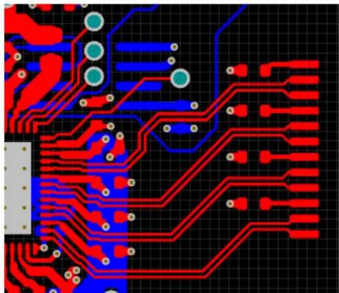
FIGURE 5: EXAMPLE MAGNETICS-TO-RJ45 DIFFERENTIAL PAIR ROUTING

RJ45 Connector
The magnetics isolate local circuitry from other equipment that the Ethernet signals connect to. The IEEE isolation test places stress on the isolated side to test the dielectric strength of the isolation. The center tap of the isolated winding has a "Bob Smith" termination through a 75 Ohm resistor and 1000 pF capacitor to chassis ground. The termination capacitor should have voltage tolerance of 3 kV.
To pass EMI compliance tests, there are a few helpful recommendations to follow:
- The RJ45 connector is recommended to have metal shielding that connects to chassis ground to reduce EMI emission.
- In order to further reduce EMI issues, micro-stripline from the external layer can be replaced with stripline between proper planes. Note that placing stripline directly on top of each other may cause capacitive coupling between channels. However, for differential pair, this coupling may be beneficial.
- It is good practice not to overlap the circuit ground plane with the chassis ground that creates coupling. Instead, make chassis ground an isolated island and make a void between the chassis and circuit ground. Place two or three 1206 pads across the chassis and circuit ground void. This would allow experimentally choosing the appropriate inductive, capacitive, or resistive components to pass EMI emission test. The 1206 pad should be located as close as practical to the power entry on the board, allowing current between the two grounds to be routed away from any sensitive circuits.
• To maximize ESD performance, the designer should consider selecting an RJ45 module without LEDs. This will simplify routing and allow greater separation in the Ethernet front end to enhance ESD/susceptibility performance. - ESD performance can also be enhanced by using a surface mount contact RJ45 connector. This may simplify routing and allow greater separation in the Ethernet front end to enhance ESD susceptibility performance.
- Placement of components for discrete and embedded RJ45 and Magnetic module:
- Distance between Ethernet device and Magnetics should be less than 1 inch of separation. If not achievable, the maximum should not be more than 3 inches.
- Distance between Magnetics and RJ45 should be less than 1 inch of separation.
- The overall length of differential pairs should be less than four inches measured from the Ethernet device to RJ-45 connector.
Magnetics
- Magnetics for Ethernet can be either integrated or discrete. Discrete modules are recommended for better EMI control.
- The magnetics module has a critical effect on overall IEEE and emission conformity. Occasionally, components that meet the basic specifications may cause the system to fail IEEE testing of interactions with other components. New magnetic modules should be carefully qualified to prevent this problem.
- Magnetics modules for 1000BASE-T Ethernet are similar to those designed for 10/100 Mbps, except that there are four differential signal pairs instead of two. Use the following guideline to verify specific electrical specification:
- Verify rated return loss is 19 dB or greater from 2 MHz through 40 MHz for 100/1000BASE-TX.
- Verify rated return loss is 12 dB or greater at 80 MHz for 100BASE-TX (the specification requires greater than or equal to 10 dB).
- Verify rated return loss is 10 dB or greater at 100 MHz for 1000BASE-TX (the specification requires greater than or equal to 8 dB).
- Verify insertion loss is less than 1.0 dB at 100 kHz through 80 MHz for 100BASE-TX.
- Verify insertion loss is less than 1.4 dB at 100 kHz through 100 MHz for 1000BASE-T.
- Verify at least 30 dB of crosstalk isolation between adjacent channels (through 150 MHz).
- Verify high voltage isolation to 15000 Vrms. (Does not apply to discrete magnetics).
-
Transmitter OCL should be greater than or equal to 350 uH with 8 mA DC bias.
-
To maximize ESD performance, the designer should consider selecting a discrete transformer as opposed to an integrated magnetic/RJ45 module. This may simplify routing and allow greater separation in the Ethernet front end to enhance ESD/susceptibility performance.
- When using discrete magnetics, it is critical to use termination: four 75 Ohm for cable-side center taps and unused pins to EFT (Electrical Fast Transient) capacitors.
- Use an EFT capacitor connected to the ground plane and 75 Ohm terminations. Suggested values are 1500 pF/2KV or 1000 pF/3KV.
A minimum of 50-mil spacing from capacitor to traces and components should be maintained.
- Implement a ground cut for high voltage installation (is not required for integrated magnetics). Typically, all planes are cleared out on the PCB in the area located halfway through the magnetics to the RJ45 connector. The TRxP/TRxN pairs should be the only traces in this cleared out region of the PCB, creating one part of the high voltage barrier required for LAN applications.
- Impedance discontinuities cause unwanted signal reflections. Minimize the number of vias (signal through hole) and other transmission line irregularities. If vias must be used, a reasonable budget is two per differential trace.
ETHRBIAS/ISET
The ETHRIAS/ISET resistor sets an internal current source reference. Thus, the ETHRIAS/ISET pin is a high impedance node and any noise induced on the ETHRIAS/ISET traces will directly impact internal current references, negatively degrading the eye-diagram quality. The ETHRIAS/ISET resistor should be placed close to the ETHRIAS/ISET pin and the ground return should be short and direct to the ground plane. Resistor traces should be very short and isolated from nearby traces.
EMI CONSIDERATIONS
PCB EMI Design Guidelines
- EMC design success must be considered during both schematic and PCB design cycles.
- EMC issues are best corrected at the source "EMC generator".
Identify Critical Circuits
- Emissions - clocks, buses and other repetitive circuits.
- Keep the hot leads short and matched if a crystal is used.
- Add small damping resistors or ferrites to the clock oscillator.
-
Control clock routing.
-
Watch out for noisy oscillator modules.
- Whenever possible, oscillators should be avoided. Oscillators increase EMI, power consumption, and jitter.
- Use a crystal if possible.
- Immunity - resets, interrupts and critic controls lines.
- Add high-frequency filters at circuit inputs.
- Control trace routing.
- Do not cross any plane splits with high-speed signal traces.
Carefully Choose Devices with EMI in Consideration
- Slower is better - rise times and clocks.
- Be careful with high-speed CMOS - for both signal and power.
Board Design
- Multilayer boards are much better for both emissions and immunity.
- Do not embed traces in power and ground planes.
Pay Close Attention to Power Decoupling
- Decouple every device with a high-frequency capacitor.
- Bypass every power input to the board with a high-frequency capacitor.
- Keep capacitor leads short.
- To improve noise and EMI in very high-speed designs, a mix of 0.1uF, 0.01uF and lower value capacitors may be used.
Concerns for I/O Circuits
• Signal, power and ground are three EMI paths through I/O.
- Add high-frequency filters to all I/O lines, even the slow ones.
- Correctly implement isolation of I/O planes.
ESD CONSIDERATIONS
- The RJ45 connector must have a metal shield to ensure the highest ESD performance.
- The metal shield of the RJ45 connector must be connected directly into the system's chassis ground plane at two points.
- All power planes and non-Ethernet traces must be cleared out from halfway under the magnetics to the RJ45 connector. Separation should be maintained for at least 0.250".
- N/S and E/W magnetic are pinned differently; therefore, selection and placement location of the magnetics is very critical for ESD performance.
• Proper layout of high-voltage barrier. - Selection and placement of the specific RJ45 connector with the chassis ground tabs as far away from the 8-pin connections may prove to be the best configuration for ESD.
- Placement of the RJ45 connector with respect to other connectors and the overall PCB location can be very important in overall ESD performance.
- Ensure that all circuitry related to and residing in the high-voltage barrier region is referenced to chassis ground only. LEDs, capacitors and anti-parallel diodes referenced to digital ground in the high-voltage barrier area will compromise the high-voltage barrier (see Figure 6).
FIGURE 6: HIGH-VOLTAGE BARRIER - EXTENDS HALFWAY THROUGH THE MAGNETICS

- Power supply voltage wires should be twisted tightly together with their return wires.
- All power entries to the PCB must be bypassed properly as close as possible to the power connector on the PCB.
- Locate the Earth ground connection(s) away from sensitive circuitry. This strategy will force the flow of an ESD occurrence away from the sensitive circuitry and direct it to Earth ground.
- All signal traces throughout the design should be kept to a minimum. Consider adding a digital ground "guard trace" to signal traces over 12" long.
- ESD occurrences can cause digital ground plane "ground bounce" if allowed to enter the digital ground plane. This can cause erratic system behavior and/or system failure. Every effort should be taken to make sure that any ESD source is not allowed to enter any digital ground or power plane on the PCB.
TROUBLESHOOTING COMMON LAYOUT ISSUES
- Lack of symmetry between the two traces within a differential pair.
Asymmetry can create common-mode noise and distort the waveforms. For each component and/or via that one trace encounters, the other trace should encounter the same component or a via at the same distance from the Ethernet silicon. - Unequal length of the two traces within a differential pair.
Inequalities create common-mode noise and will distort the transmitting or receiving waveforms. - Excessive distance between the Ethernet silicon and the magnetics.
Long traces on FR4 fiberglass epoxy substrate will attenuate the analog signals. In addition, any impedance mismatch in the traces will be aggravated if they are longer than the four-inch guideline. - Routing any other trace parallel to and close to one of the differential traces.
Crosstalk onto the receive channel will cause degraded long cable BER (Bit Error Rate). Crosstalk onto the transmit channel can cause excessive EMI emissions and can cause poor transmit BER on long cables. At a minimum, other signals should be kept 0.3 inches from the differential traces. - Routing one pair of differential traces too close to another pair of differential traces.
After exiting the Ethernet silicon, the trace pairs should be kept 0.3 inches or more away from the other trace pairs. The only possible exceptions are in the vicinities where the traces enter or exit the magnetics, the RJ-45 connector, and the Ethernet silicon. - Use of a low-quality magnetics module.
- Incorrect differential trace impedances.
Short traces will have fewer problems if the differential impedance is slightly off target.
APPENDIX A: APPLICATION NOTE REVISION HISTORY
TABLE A-1: REVISION HISTORY
| Revision Level & Date Section/Figure/Entry Correction | ||
| DS00002054A (02-16-16) All | Initial release | |
Note the following details of the code protection feature on Microchip devices:
• Microchip products meet the specification contained in their particular Microchip Data Sheet.
- Microchip believes that its family of products is one of the most secure families of its kind on the market today, when used in the intended manner and under normal conditions.
- There are dishonest and possibly illegal methods used to breach the code protection feature. All of these methods, to our knowledge, require using the Microchip products in a manner outside the operating specifications contained in Microchip's Data Sheets. Most likely, the person doing so is engaged in theft of intellectual property.
• Microchip is willing to work with the customer who is concerned about the integrity of their code.
- Neither Microchip nor any other semiconductor manufacturer can guarantee the security of their code. Code protection does not mean that we are guaranteeing the product as "unbreakable."
Code protection is constantly evolving. We at Microchip are committed to continuously improving the code protection features of our products. Attempts to break Microchip's code protection feature may be a violation of the Digital Millennium Copyright Act. If such acts allow unauthorized access to your software or other copyrighted work, you may have a right to sue for relief under that Act.
Information contained in this publication regarding device applications and the like is provided only for your convenience and may be superseded by updates. It is your responsibility to ensure that your application meets with your specifications. MICROCHIP MAKES NO REPRESENTATIONS OR WARRANTIES OF ANY KIND WHETHER EXPRESS OR IMPLIED, WRITTEN OR ORAL, STATUTORY OR OTHERWISE, RELATED TO THE INFORMATION, INCLUDING BUT NOT LIMITED TO ITS CONDITION, QUALITY, PERFORMANCE, MERCHANTABILITY OR FITNESS FOR PURPOSE. Microchip disclaims all liability arising from this information and its use. Use of Microchip devices in life support and/or safety applications is entirely at the buyer's risk, and the buyer agrees to defend, indemnify and hold harmless Microchip from any and all damages, claims, suits, or expenses resulting from such use. No licenses are conveyed, implicitly or otherwise, under any Microchip intellectual property rights unless otherwise stated.
Trademarks
The Microchip name and logo, the Microchip logo, AnyRate, dsPIC, FlashFlex, flexPWR, Heldo, JukeBlox, KeeLoq, KeeLoq logo, Kleer, LANCheck, LINK MD, MediaLB, MOST, MOST logo, MPLAB, OptoLyzer, PIC, PICSTART, PIC32 logo, RightTouch, SpyNIC, SST, SST Logo, SuperFlash and UNI/O are registered trademarks of Microchip Technology Incorporated in the U.S.A. and other countries.
ClockWorks, The Embedded Control Solutions Company, ETHERSYNCH, Hyper Speed Control, HyperLight Load, IntelliMOS, mTouch, Precision Edge, and QUIET-WIRE are registered trademarks of Microchip Technology Incorporated in the U.S.A.
Analog-for-the-Digital Age, Any Capacitor, AnyIn, AnyOut, BodyCom, chipKIT, chipKIT logo, CodeGuard, dsPICDEM, dsPICDEM.net, Dynamic Average Matching, DAM, ECAN, EtherGREEN, In-Circuit Serial Programming, ICSP, Inter-Chip Connectivity, JitterBlocker, KleerNet, KleerNet logo, MiWi, motorBench, MPASM, MPF, MPLAB Certified logo, MPLIB, MPLINK, MultiTRAK, NetDetach, Omniscient Code Generation, PICDEM, PICDEM.net, PICkit, PICtail, PureSilicon, RightTouch logo, REAL ICE, Ripple Blocker, Serial Quad I/O, SQI, SuperSwitcher, SuperSwitcher II, Total Endurance, TSHARC, USBCheck, VariSense, ViewSpan, WiperLock, Wireless DNA, and ZENA are trademarks of Microchip Technology Incorporated in the U.S.A. and other countries.
SQTP is a service mark of Microchip Technology Incorporated in the U.S.A.
Silicon Storage Technology is a registered trademark of Microchip Technology Inc. in other countries.
GestIC is a registered trademarks of Microchip Technology Germany II GmbH & Co. KG, a subsidiary of Microchip Technology Inc., in other countries.
All other trademarks mentioned herein are property of their respective companies.
© 2016, Microchip Technology Incorporated, Printed in the U.S.A., All Rights Reserved.
ISBN: 9781522401377
QUALITY MANAGEMENT SYSTEM
CERTIFIED BY DNV
=ISO/TS 16949=
Microchip received ISO/TS-16949:2009 certification for its worldwide headquarters, design and wafer fabrication facilities in Chandler and Tempe, Arizona; Gresham, Oregon and design centers in California and India. The Company's quality system processes and procedures are for its PIC® MCUs and dsPIQ® DSCs, KEELOC® code hopping devices, Serial EEPROMs, microperipherals, nonvolatile memory and analog products. In addition, Microchip's quality system for the design and manufacture of development systems is ISO 9001:2000 certified.
Worldwide Sales and Service
AMERICAS
Corporate Office
2355 West Chandler Blvd.
Chandler, AZ 85224-6199
Tel: 480-792-7200
Fax: 480-792-7277
Technical Support:
http://www.microchip.com/
support
Web Address:
www.microchip.com
Atlanta
Duluth, GA
Tel: 678-957-9614
Fax: 678-957-1455
Austin, TX
Tel: 512-257-3370
Boston
Westborough, MA
Tel: 774-760-0087
Fax: 774-760-0088
Chicago
Itasca, IL
Tel: 630-285-0071
Fax: 630-285-0075
Cleveland
Independence, OH
Tel: 216-447-0464
Fax: 216-447-0643
Dallas
Addison, TX
Tel: 972-818-7423
Fax: 972-818-2924
Detroit
Novi, MI
Tel: 248-848-4000
Houston, TX
Tel: 281-894-5983
Indianapolis
Noblesville, IN
Tel: 317-773-8323
Fax: 317-773-5453
Los Angeles
Mission Viejo, CA
Tel: 949-462-9523
Fax: 949-462-9608
New York, NY
Tel: 631-435-6000
San Jose, CA
Tel: 408-735-9110
Canada - Toronto
Tel: 905-673-0699
Fax: 905-673-6509
ASIA/PACIFIC
Asia Pacific Office
Suites 3707-14, 37th Floor
Tower 6, The Gateway
Harbour City, Kowloon
Hong Kong
Tel: 852-2943-5100
Fax: 852-2401-3431
Australia - Sydney
Tel: 61-2-9868-6733
Fax: 61-2-9868-6755
China - Beijing
Tel: 86-10-8569-7000
Fax: 86-10-8528-2104
China - Chengdu
Tel: 86-28-8665-5511
Fax: 86-28-8665-7889
China - Chongqing
Tel: 86-23-8980-9588
Fax: 86-23-8980-9500
China - Dongguan
Tel: 86-769-8702-9880
China - Hangzhou
Tel: 86-571-8792-8115
Fax: 86-571-8792-8116
China - Hong Kong SAR
Tel: 852-2943-5100
Fax: 852-2401-3431
China - Nanjing
Tel: 86-25-8473-2460
Fax: 86-25-8473-2470
China - Qingdao
Tel: 86-532-8502-7355
Fax: 86-532-8502-7205
China - Shanghai
Tel: 86-21-5407-5533
Fax: 86-21-5407-5066
China - Shenyang
Tel: 86-24-2334-2829
Fax: 86-24-2334-2393
China - Shenzhen
Tel: 86-755-8864-2200
Fax: 86-755-8203-1760
China - Wuhan
Tel: 86-27-5980-5300
Fax: 86-27-5980-5118
China - Xian
Tel: 86-29-8833-7252
Fax: 86-29-8833-7256
ASIA/PACIFIC
China - Xiamen
Tel: 86-592-2388138
Fax: 86-592-2388130
China - Zhuhai
Tel: 86-756-3210040
Fax: 86-756-3210049
India - Bangalore
Tel: 91-80-3090-4444
Fax: 91-80-3090-4123
India - New Delhi
Tel: 91-11-4160-8631
Fax: 91-11-4160-8632
India - Pune
Tel: 91-20-3019-1500
Japan - Osaka
Tel: 81-6-6152-7160
Fax: 81-6-6152-9310
Japan - Tokyo
Tel: 81-3-6880-3770
Fax: 81-3-6880-3771
Korea - Daegu
Tel: 82-53-744-4301
Fax: 82-53-744-4302
Korea - Seoul
Tel: 82-2-554-7200
Fax: 82-2-558-5932 or
82-2-558-5934
Malaysia - Kuala Lumpur
Tel: 60-3-6201-9857
Fax: 60-3-6201-9859
Malaysia - Penang
Tel: 60-4-227-8870
Fax: 60-4-227-4068
Philippines - Manila
Tel: 63-2-634-9065
Fax: 63-2-634-9069
Singapore
Tel: 65-6334-8870
Fax: 65-6334-8850
Taiwan - Hsin Chu
Tel: 886-3-5778-366
Fax: 886-3-5770-955
Taiwan - Kaohsiung
Tel: 886-7-213-7828
Taiwan - Taipei
Tel: 886-2-2508-8600
Fax: 886-2-2508-0102
Thailand - Bangkok
Tel: 66-2-694-1351
Fax: 66-2-694-1350
EUROPE
Austria - Wels
Tel: 43-7242-2244-39
Fax: 43-7242-2244-393
Denmark - Copenhagen
Tel: 45-4450-2828
Fax: 45-4485-2829
France - Paris
Tel: 33-1-69-53-63-20
Fax: 33-1-69-30-90-79
Germany - Dusseldorf
Tel: 49-2129-3766400
Germany - Karlsruhe
Tel: 49-721-625370
Germany - Munich
Tel: 49-89-627-144-0
Fax: 49-89-627-144-44
Italy - Milan
Tel: 39-0331-742611
Fax: 39-0331-466781
Italy - Venice
Tel: 39-049-7625286
Netherlands - Drunen
Tel: 31-416-690399
Fax: 31-416-690340
Poland - Warsaw
Tel: 48-22-3325737
Spain - Madrid
Tel: 34-91-708-08-90
Fax: 34-91-708-08-91
Sweden - Stockholm
Tel: 46-8-5090-4654
UK - Wokingham
Tel: 44-118-921-5800
Fax: 44-118-921-5820

- GIGABIT ETHERNET DESIGN GUIDE
- INTRODUCTION
- GENERAL PCB LAYOUT GUIDELINES
- POWER SUPPLY CONSIDERATION
- DEVICE DECOUPLING
- PCB BYPASSING
- PCB BULK CAPACITORS
- PCB LAYER STRATEGY
- RECOMMENDED LAYER STACKS LAYOUT
- SIGNAL INTEGRITY CONCERNS
- PCB TRACE CONSIDERATIONS
- CRYSTAL CIRCUITRY
- VIAS IN GROUND FLAG (EXPOSED PAD)
- USB LAYOUT GUIDELINES
- ETHERNET LAYOUT GUIDELINES
- ETHERNET DIFFERENTIAL PAIRS
- RJ45 CONNECTOR
- MAGNETICS
- ETHRBIAS/ISET
- EMI CONSIDERATIONS
- PCB EMI DESIGN GUIDELINES
- IDENTIFY CRITICAL CIRCUITS
- CAREFULLY CHOOSE DEVICES WITH EMI IN CONSIDERATION
- BOARD DESIGN
- PAY CLOSE ATTENTION TO POWER DECOUPLING
- CONCERNS FOR I/O CIRCUITS
- ESD CONSIDERATIONS
- TROUBLESHOOTING COMMON LAYOUT ISSUES
- APPENDIX A: APPLICATION NOTE REVISION HISTORY
- NOTE THE FOLLOWING DETAILS OF THE CODE PROTECTION FEATURE ON MICROCHIP DEVICES
- TRADEMARKS
- WORLDWIDE SALES AND SERVICE
- AMERICAS
- ASIA/PACIFIC
- EUROPE
Brand : Microchip
Model : LAN7801
Category : Documentation technique