
ATF15xx-DK3-U - Electronic development kit Microchip - Free user manual and instructions
Find the device manual for free ATF15xx-DK3-U Microchip in PDF.


| Product Type | Development Kit |
| Brand | Microchip |
| Model | ATF15xx-DK3-U |
| Supported Devices | ATF15xx CPLD family |
| Interface | USB 2.0 |
| Power Supply | USB bus-powered (5V) |
| Dimensions (approx.) | 100 mm x 80 mm x 20 mm |
| Weight (approx.) | 50 g |
| Programming Software | Atmel-ICE or compatible |
| Included Accessories | USB cable, quick start guide |
| Primary Function | Programming and debugging of ATF15xx CPLDs |
| Operating Temperature | 0°C to 70°C |
| Storage Temperature | -40°C to 85°C |
| Regulatory Certifications | CE, FCC |
| Maintenance | Keep dry; clean with dry cloth |
| Safety Precautions | Use ESD mat; avoid moisture |
| Spare Parts Availability | Contact Microchip support |
| Repairability | Not user-serviceable; contact support |
Frequently Asked Questions - ATF15xx-DK3-U Microchip
User questions about ATF15xx-DK3-U Microchip
0 question about this device. Answer the ones you know or ask your own.
Ask a new question about this device
Download the instructions for your Electronic development kit in PDF format for free! Find your manual ATF15xx-DK3-U - Microchip and take your electronic device back in hand. On this page are published all the documents necessary for the use of your device. ATF15xx-DK3-U by Microchip.
USER MANUAL ATF15xx-DK3-U Microchip
The Atmel ® ATF15xx-DK3-U Complex Programmable Logic Device (CPLD) Development/Programmer Kit is a complete development system and an In-System Programming (ISP) programmer for the Atmel ATF15xx Family of industry standard pin compatible CPLDs with Logic Doubling ® features. This kit provides designers a very quick and easy way to develop prototypes and evaluate new designs with an ATF15xx ISP CPLD. The ATF15xx Family of ISP CPLDs includes the Atmel ATF15xxAS, ATF15xxASL, ATF15xxASV, and ATF15xxASVL CPLDs. With the availability of the different socket adapter boards to support most of the package types (1) offered in the ATF15xx Family of ISP CPLDs, this kit can be used as an ISP programmer to program the ATF15xx ISP CPLDs in most of the available package types (1) through the industry standard JTAG interface (IEEE 1149.1).
Kit Contents
CPLD Development/Programmer Board (ATF15xx-DK3)
44-pin TQFP Socket Adapter Board (ATF15xxDK3-SAA44) (2)
- ATF15xx USB-based JTAG ISP Download Cable (ATDH1150USB or ATDH1150USB-K)
• Two Atmel 44-pin TQFP Sample Devices
Device Support
The ATF15xx-DK3-U CPLD Development/Programmer Kit supports the following devices in all currently available Atmel speed grades and packages (except the 100-PQFP):
• ATF1502AS/ASL
• ATF1504AS/ASL
• ATF1508ASV/ASVL
• ATF1502ASV
• ATF1504ASV/ASVL
• ATF1508AS/ASL

- The socket adapter board is not offered for the 100-pin PQFP.
- Only the 44-pin TQFP Socket Adapter Board is included in this kit. Other socket adapter boards are sold separately. See "Hardware Description" section for more information on socket adapter board ordering codes.
Table of Contents
Kit Features 3
CPLD Development/Programmer Board 3
Logic Doubling CPLDs 3
ATF15xx ISP Download Cable....3
PLD Development Software 3
System Requirements 3
Ordering Information....4
Hardware Description 4
CPLD Development/Programmer Board 4
7-segment Displays with Selectable Jumpers 5
LEDs with Selectable Jumpers 7
Push-button Switches with Selectable Jumpers for I/O Pins 8
Push-button Switches with Selectable Jumpers for GCLR and OE1 Pins 9
2MHz Oscillator and Clock Selection Jumper 10
VccIO and VccINT Voltage Selection Jumpers and LEDs 11
IccIO and IccINT Jumpers 11
Voltage Regulators 11
Power Supply Switch and Power LED 11
Power Supply Jack and Power Supply Header 11
JTAG ISP Connector and TDO Selection Jumper 12
Socket Adapter Board 14
Atmel ATF15xx ISP Download Cable.... 14
Schematic Diagrams 15
References and Support 20
Atmel ProChip Designer Software 20
Atmel WinCUPL Software 20
Atmel ATMISP Software....20
Atmel POF2JED Conversion Software....20
Technical Support 21
Revision History 21
Kit Features
CPLD Development/Programmer Board
10-pin JTAG-ISP Port
• Regulated Power Supply Circuits for 9VDC Power Source
- Selectable 5V, 3.3V, 2.5V, or 1.8V I/O Voltage Supply
- Selectable 1.8V, 3.3V, or 5.0V Core Voltage Supply
• 44-pin TQFP Socket Adapter Board
- Headers for I/O Pins of the ATF15xx Device
• 2MHz Crystal Oscillator
• Four 7-segment LED Displays
• Eight Individual LEDs
• Eight Push-button Switches
- Global Clear and Output Enable Push-button Switches
• Current Measurement Jumpers
Logic Doubling CPLDs
• ATF15xx ISP CPLD with Logic Doubling Architecture
ATF15xx ISP Download Cable
5V, 3.3V, 2.5V, or 1.8V ISP Download Cable for the Universal Serial Bus (USB) port of a PC
There are two versions of the ATF15xx USB ISP Download Cable; ATDH1150USB and ATDH1150USB-K. They are built by two different vendors but have identical circuit design, and the Atmel Ordering Code is ATDH1150USB. The ATDH1150USB-K is built by Kanda (www.kanda.com) and it can be directly purchased from Kanda. More details are available online at www.atmel.com/tools/ATDH1150USB.aspx.
PLD Development Software
The Atmel PLD development software tools are available online for PLD designer's use of the ATF15xx ISP CPLDs. Please reference the Overview document, "PLD Design Software Overview" available at:
http://www.atmel.com/images/atmel-3629-pld-design-software-overview.pdf
System Requirements
The minimum hardware and software required to program an ATF15xx ISP CPLD device designed using the Atmel ProChip Designer Software on the CPLD Development/Programmer Board through the Atmel ATMISP (ATF15xx CPLD ISP Software) are:
• x86 or x64 Microprocessor-based Computer
- Windows XP or Windows 7
128-MByte RAM
500-MByte Free Hard Disk Space
- Windows-supported Mouse
• Available USB 1.1 / 2.0 / 3.0 Port
- 9VDC Power Supply with 500mA of Supply Current
• SVGA Monitor (800 x 600 Resolution)
Ordering Information
| Atmel Part Number Description | |
| ATF15xx-DK3-U | CPLD Development/Programmer Kit (includes the ATF15xxDK3-SAA44 (1) and ATDH1150USB or ATDH1150USB-K) |
| ATF15xxDK3-SAA100 100-pin TQFP Socket Adapter Board for DK3 Board | |
| ATF15xxDK3-SAJ44 44-pin PLCC Socket Adapter Board for DK3 Board | |
| ATF15xxDK3-SAJ84 84-pin PLCC Socket Adapter Board for DK3 Board | |
| ATF15xxDK3-SAA44 (1) | 44-pin TQFP Socket Adapter Board for DK3 Board |
Note: 1. Only the 44-pin TQFP Socket Adapter Board is included in this kit. Other socket adapter boards are sold separately. See "Hardware Description" section for more information on socket adapter board ordering codes.
Hardware Description
CPLD Development/Programmer Board
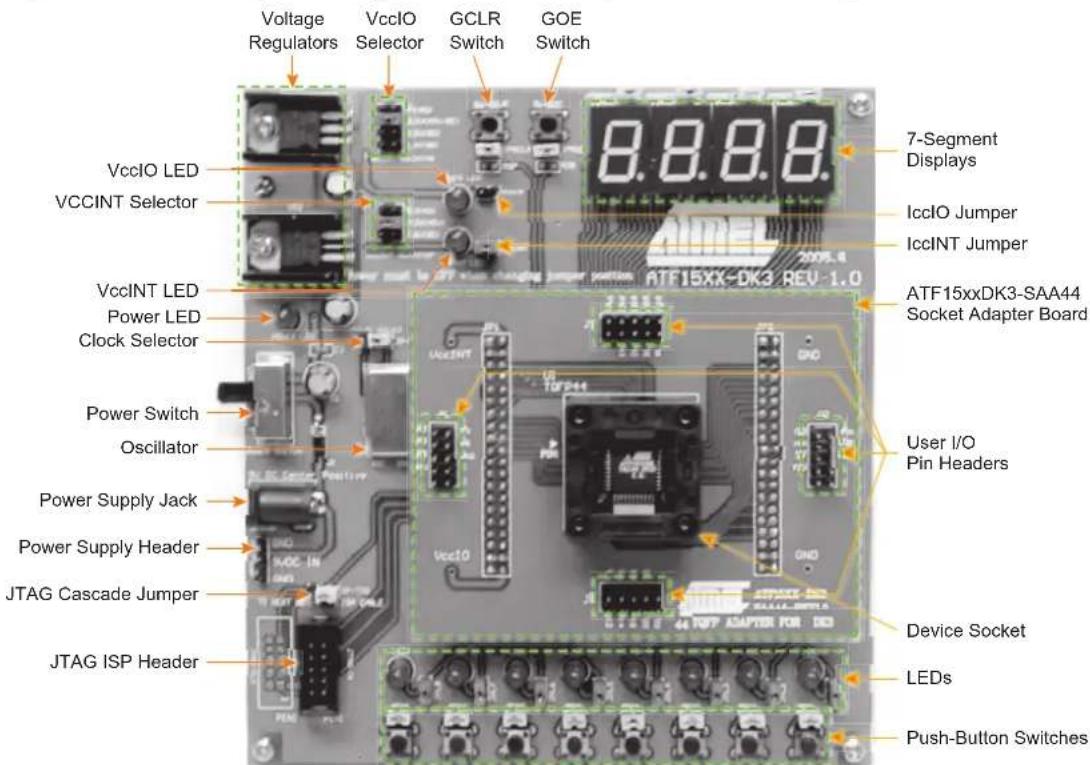
The CPLD Development/Programmer and Socket Adapter Boards shown in the below figure contain features that are useful for developing, prototyping, or evaluating ATF15xx CPLD designs. Features that make this a very versatile starter/development kit and an ISP programmer for the ATF15xx family of JTAG-ISP CPLDs include:
- Push-button Switches
• LEDs
7-segment Displays
• 2MHz Crystal Oscillator
5V, 3.3V, 2.5V, or 1.8V V cc IO Selector
1.8V, 3.3V, or 5.0V V CCINT Selector
- JTAG ISP Port
- Socket Adapters
Figure 1. CPLD Development/Programmer Kit with 44-pin TQFP Socket Adapter Board
7-segment Displays with Selectable Jumpers
The CPLD Development/Programmer Board contains four 7-segment displays which allow the observation of the ATF15xx CPLD outputs. These four displays are labeled as DSP1, DSP2, DSP3, and DSP4. The 7-segment displays have common anode LEDs with the common anode lines connected to the VCCIO (I/O supply voltage for the CPLD) through a series of resistors with selectable jumpers labeled as JPDSP1, JPDSP2, JPDSP3, and JPDSP4. These jumpers can be removed to disable the displays by unconnecting the Vcc IO to the displays. Individual cathode lines are connected to the I/O pins of the ATF15xx CPLD on the CPLD Development/Programmer Kit. To turn on a particular segment, including the DOT of a display, the corresponding ATF15xx I/O pin connected to this LED segment must be in a logic low state with the corresponding selectable jumper set; therefore, the outputs of the ATF15xx device will require configuration for active-low outputs in the design file. The displays work best at 2.5V Vcc IO or higher.
Each segment of each display is hard-wired to one specific I/O pin of the ATF15xx device. For the higher pin count devices (100-pin and larger), all seven segments and the DOT segments of the four displays are connected to the I/O pins; however, for the lower pin count devices, only a subset of the displays, first and fourth displays, are connected to the ATF15xx device's I/O pins. Tables 1 and 2 show the 7-segment display package connections to the ATF15xx device. The circuit schematic of the displays and jumpers is shown in the figure below.
Figure 2. Circuit Diagram of 7-segment Display and Jumpers
![graph TD A["VccIO"] --> B["JPDSPI1"] A --> C["JPLED1"] B --> D["DSP1"] C --> E["DSP2"] D --> F["VD1: a f b c d"] E --> G["VD2: a f b c d"] F --> H["RDSP11: RDSP13"] F --> I["RDSP14: RDSP15"] F --> J["RDSP16: RDSP17"] G --> K["RDSP21: RDSP23"] G --> L["RDSP24: RDSP25"] G --> M["RDSP26: RDSP27"] H -->…](/content/2026/05/832182/images/00610e5d5752eb7c204e1d8b0cb23f801c45f51605312566f38f3ae585ce0be9.jpg)
Table 1. ATF15xx 44-pin Connections to 7-segment Displays
| 44-pin TQFP 44-pin PLCC | |||
| DSP/Segment | PLD Pin | DSP/Segment PLD | Pin DSP |
| 1/A 27 3/A NC | 1/A 33 | 3/A NC | |
| 1/B 33 3/B NC | 1/B 39 | 3/B NC | |
| 1/C 30 3/C NC | 1/C 36 | 3/C NC | |
| 1/D 21 3/D NC | 1/D 27 | 3/D NC | |
| 1/E 18 3/E NC | 1/E 24 | 3/E NC | |
| 1/F 23 3/F NC | 1/F 29 | 3/F NC | |
| 1/G 20 3/G NC | 1/G 26 | 3/G NC | |
| 1/DOT 31 3/DOT NC | 1/DOT 37 3/DOT | ||
| 2/A | NC | 4/A | 3 |
| 2/B | NC | 4/B | 10 |
| 2/C | NC | 4/C | 6 |
| 2/D | NC | 4/D | 43 |
| 2/E | NC | 4/E | 35 |
| 2/F | NC | 4/F | 42 |
| 2/G | NC | 4/G | 34 |
| 2/DOT | NC | 4/DOT | 11 |
| Segment PLD Pin | DSP/Segment PLD Pin | |
| 2/A | NC | 4/A |
| 2/B | NC | 4/B |
| 2/C | NC | 4/C |
| 2/D | NC | 4/D |
| 2/E | NC | 4/E |
| 2/F | NC | 4/F |
| 2/G | NC | 4/G |
| 2/DOT | NC | 4/DOT |
Table 2. ATF15xx 84-pin and 100-pin Connections to 7-segment Displays
| 84-pin PLCC | |||
| DSP/Segment | PLD Pin | DSP/Segment | PLD Pin |
| 1/A | 68 | 3/A | 22 |
| 1/B | 74 | 3/B | 28 |
| 1/C | 70 | 3/C | 25 |
| 1/D | 63 | 3/D | 21 |
| 1/E | 58 | 3/E | 16 |
| 1/F | 65 | 3/F | 17 |
| 1/G 61 3/G 12 | 1/G 60 | 3/G | |
| 1/DOT | 73 | 3/DOT | 29 |
| 2/A | 52 | 4/A | 5 |
| 2/B | 57 | 4/B | 10 |
| 2/C | 55 | 4/C | 8 |
| 2/D | 48 | 4/D | 79 |
| 2/E | 41 | 4/E | 76 |
| 2/F | 50 | 4/F | 77 |
| 2/G 45 4/G 75 | 2/G 45 | 4/G | |
| 2/DOT | 56 | 4/DOT | 11 |
| 100-pin TQFP | |||
| DSP/Segment | PLD Pin | DSP/Segment | PLD Pin |
| 1/A | 67 | 3/A | 13 |
| 1/B | 71 | 3/B | 19 |
| 1/C | 69 | 3/C | 16 |
| 1/D | 61 | 3/D | 8 |
| 1/E | 57 | 3/E | 83 |
| 1/F | 64 | 3/F | 6 |
| 92 | |||
| 1/DOT | 75 | 3/DOT | 20 |
| 2/A | 52 | 4/A | 100 |
| 2/B | 54 | 4/B | 94 |
| 2/C | 47 | 4/C | 97 |
| 2/D | 41 | 4/D | 81 |
| 2/E | 46 | 4/E | 76 |
| 2/F | 40 | 4/F | 80 |
| 79 | |||
| 2/DOT | 56 | 4/DOT | 93 |
LEDs with Selectable Jumpers
The CPLD Development/Programmer Board has eight individual LEDs, which allow designers to display the output signals from the user I/Os of the ATF15xx devices. These eight LEDs are labeled LED1 to LED8 on the CPLD Development/Programmer Board. The cathode of each LED is connected to Ground (GND) through a series resistor, while the anode of each LED is connected to a user I/O pin of the CPLD through the JPL1/2/3/4/5/6/7/8 selectable jumper. These jumpers can be removed to disable the LEDs by unconnecting the anodes of the LEDs to the I/O pins of the CPLD. The figure below illustrates the circuit diagram of the LEDs with the selection jumpers.
To turn on a particular LED, the corresponding ATF15xx I/O pin connected to the LED must be in a logic high state with the corresponding jumper set; therefore, the outputs of the ATF15xx device will need to be configured as active high outputs. The LEDs work best at 2.5V V CC IO or higher.
The lower pin count devices (44-pin) only have four I/Os connected to LED1/2/3/4. For the higher pin-count devices (100-pin and larger), all eight LEDs are connected to the I/Os of the device. Table 3 shows the different package connections of the CPLD I/Os to the LEDs.
Figure 3. Circuit Diagram of the LEDs and Jumpers
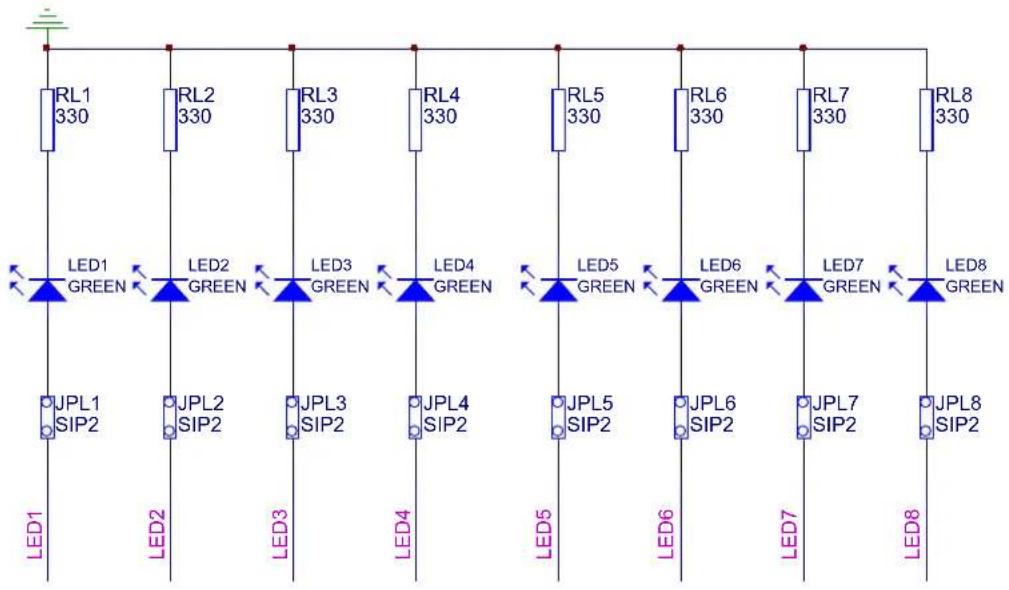
Table 3. ATF15xx Connections to LEDs
| 44-pin TQFP 44-pin | CC 84-pin PLCC 100-pin | ||
| LED PLD Pin LED P | Pin LED PLD Pin LED P | ||
| LED1 28 | LED1 34 LED1 69 | LED1 68 | |
| LED2 25 | LED2 31 LED2 67 | LED2 65 | |
| LED3 22 | LED3 28 LED3 64 | LED3 63 | |
| LED4 19 | LED4 25 LED4 60 | LED4 58 | |
| FP | |
| n | |
| LED5 27 | LED5 17 |
| LED6 24 | LED6 14 |
| LED7 18 | LED7 10 |
| LED8 15 | LED8 9 |
Push-button Switches with Selectable Jumpers for I/O Pins
The CPLD Development/Programmer Board contains eight push-button switches, which are connected to the I/O pins of the CPLD. The switches send input logic signals to the user I/O pins of the ATF15xx device. These switches are labeled SW1 to SW8 on the CPLD Development/Programmer Board. One end of each input push-button switch is connected to VCCIO , while the other end of each push-button switch is connected to a pull-down resistor and then connected to the specific I/O pin of the CPLD through the JPS1/2/3/4/5/6/7/8 selectable jumper.
If any one of these switches is pressed and the corresponding jumper is set, the specific I/O pin of the device will be driven to a logic high state by the output of switch circuit. Since each push-button switch is also connected to a pull-down resistor, the input will have a logic low state if the switch is not pressed with the corresponding jumper set. If the push-button jumper is not set, the corresponding pin will be treated as an unconnected pin. Figure 4 is a circuit diagram of the push-button switch and selectable jumper. Table 4 shows the connections of these eight push-button switches to the CPLD I/O pins in the different package types.
Figure 4. Circuit Diagram of the Push-button Switches and Jumpers for the I/O Pins

Table 4. ATF15xx Connections to the I/O Pin Switches
| 44-pin TQFP 44-pin LCC 84-pin PLCC 100-pin QFP | ||||||||
| Push Button | PLD Pin | Push Button | PLD Pin Push B | on PLD Pin Push Button | LD Pin | |||
| SW1 15 | SW1 21 | SW1 54 | SW1 48 | |||||
| SW2 14 | SW2 20 | SW2 51 | SW2 36 | |||||
| SW3 13 | SW3 19 | SW3 49 | SW3 44 | |||||
| SW4 12 | SW4 18 | SW4 44 | SW4 37 | |||||
| SW5 8 | SW5 14 | SW5 9 | SW5 96 | |||||
| SW6 5 | SW6 11 | SW6 6 | SW6 98 | |||||
| SW7 2 | SW7 8 | SW7 4 | SW7 84 | |||||
| SW8 44 | SW8 6 | SW8 80 | SW8 99 | |||||
Push-button Switches with Selectable Jumpers for GCLR and OE1 Pins
The CPLD Development/Programmer Board contains two push-button switches for the Global Clear (GCLR) and Output Enable (OE1) pins of the CPLD. The switches control the logic states of the OE1 and GCLR inputs of the ATF15xx devices. These switches are labeled SW-GCLR and SW-GOE1 on the board. One end of the SW-GCLR input push-button switch is connected to GND. The other end of the push-button switch is connected to a pull-up resistor to VCCIO , and then connected to the GCLR dedicated input pin of the ATF15xx device. It is intended to be used as an active-low reset signal to reset the registers in the ATF15xx device with the JPGCLR selectable jumper set. Similarly, one end of the SW-GOE1 input push-button switch is connected to GND. The other end of the push-button switch is connected to a pull-up resistor to VCCIO , and then connected to the OE1 dedicated input pin of the ATF15xx device. It is intended to be used as an active-low output enable signal to control the enabling/disabling of the tri-state output buffers in the ATF15xx with the JPGOE selectable jumper set.
Figure 5 is the circuit diagram of the push-button switches and the jumpers for the GCLR and OE1 pins.
If any of these push-button switches is pressed and the corresponding jumper is set, the specific I/O of the CPLD will be driven to a logic low state. Since each push-button is also connected to a pull-up resistor, the corresponding CPLD input will have a logic high state if the push-button switch is not pressed with the corresponding selectable jumper set. If the selectable jumper is not set, the corresponding dedicated input pin of the CPLD can be considered a No Connect (NC) pin. Table 5 shows the pin numbers of the GCLR and OE1 dedicated input pins of the ATF15xx devices in all available package types.
Figure 5. Circuit Diagram of Push-button Switches and Selectable Jumpers for GCLR and OE1

Table 5. Pin Numbers of GCLR and OE1
| 44-pin TQFP 44-pin PLCC 84-pin PLCC 100-pin TQFP | ||||
| GCLR 39 1 | 1 89 | |||
| OE1 38 44 | 84 88 | |||
2MHz Oscillator and Clock Selection Jumper
The Clock Selection Jumper labeled JP-GCLK on the CPLD Development/Programmer Board is a two-position jumper that allows the users to select which GCLK dedicated input pin (either GCLK1 or GCLK2) of the ATF15xx device should be connected to the output of the 2MHz oscillator. In addition, the jumper can be removed to allow an external clock source to be connected to GCLK1 and/or GCLK2 of the ATF15xx device. Figure 6 is an illustration of the circuit diagram of the oscillator and selection jumper. Table 6 shows the pin numbers for the GCLK1 and GCLK2 dedicated input pins of the ATF15xx device in all the different available package types.

If GCLK1 jumper is set, the jumper will be located toward the side of the board. On the other hand, if GCLK2 jumper is set, the jumper will be located toward the middle of the board.
Figure 6. Circuit Diagram of Oscillator and Clock Selection Jumper
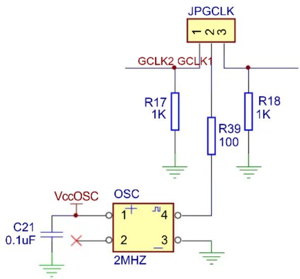
Table 6. Pin Numbers of GCLK1 and GCLK2
| 44-pin TQFP 44-pin PLCC 84-pin PLCC | 100-pin TQFP | ||
| GCLK1 37 43 83 87 | |||
| GCLK2 40 2 2 90 |
VccIO and VccINT Voltage Selection Jumpers and LEDs
The Vcc IO and Vcc INT Voltage Selection Jumpers, labeled VCCIO Selector and VCCINT Selector respectively on ATF15xx-DK3 Development/Programming Kit, allow the selection of the I/O supply voltage level ( Vcc IO) and core supply voltage level ( Vcc INT) that are used for the target CPLD on the kit. Once these jumpers are set correctly, the LEDs (labeled VCCINT LED and VCCIO LED) will turn on; however, at lower supply voltage levels (i.e. 2.5V or lower), the LEDs might be very dim.
- For ATF15xxAS/ASL (5.0V) CPLDs, both the VCCIO Selector and VCCINT Selector jumpers must be set to 5.0V.
- For ATF15xxASV/ASVL (3.3V) CPLDs, both the VCCIO Selector and VCCINT Selector Jumpers must be set to 3.3V only.

The power of the CPLD Development/Programmer Kit must be turned OFF when changing the position of the VCCIO or VCCINT Voltage Selection Jumper (VCCIO Selector or VCCINT Selector).
IccIO and IccINT Jumpers
The ICCIO and ICCINT jumpers can be removed and used as ICC measurement points. When the jumpers are removed, current meters can be connected to the posts to measure the current consumption of the target CPLD. When users are not using these jumpers to measure the current, these jumpers must be set in order for the kit and CPLD to operate.
Voltage Regulators
Two voltage regulators, labeled VR1 and VR2, are used to independently generate and regulate the VCC INT and VCC IO voltages from the 9VDC power supply. For details, please see the ATF15xx-DK3 kit schematic, Figure 11.
Power Supply Switch and Power LED
The Power Supply Switch, labeled POWER SWITCH, can be switched to the on or off position, which is used to turn on or off the power of the ATF15xx-DK3 board respectively. It allows the 9VDC voltage at the Power Supply Jack to pass to the voltage regulators when it is in the on position. When the Power Supply Switch is turned on, the Power LED (labeled POWER LED) will light up to indicate that the ATF15xx-DK3 Kit is supplied with power.
Power Supply Jack and Power Supply Header
The ATF15xx-DK3 board contains two different types of power supply connectors labeled JPower and JP Power. Either one of these power supply connectors can be used to connect a 9VDC power source to the kit. The first power connector labeled JPower, is a barrel power jack with a 2.1mm diameter post, and it mates to a 2.1mm (inner diameter) x 5.5mm (outer diameter) female plug. The second power supply header labeled JP Power, is a 4-pin male 0.100" header with 0.025" square posts. The availability of these two types of power connectors allows the users to choose the type of power supply equipment to use for ATF15xx-DK3 Development/Programmer Kit.

Only one of these two power supply connectors should be powered with a 9VDC source but not both at the same time.
JTAG ISP Connector and TDO Selection Jumper
The JTAG ISP Connector labeled JTAG-IN, is used to connect the ATF15xx JTAG port pins (TCK, TDI, TMS, and TDO) through the ISP download cable to the parallel printer (LPT) port of a PC for JTAG ISP programming of the ATF15xx device. Polarized connectors are used on the ATF15xx-DK3 and ISP Download Cable to minimize connection problems. The PIN1 label at the bottom of the JTAG ISP connector indicates the pin 1 position of the 10-pin header and further reduces the chance of connecting the ISP Download Cable incorrectly.
To the left of the JTAG-IN connector, there are two columns of vias, and they are labeled JTAG-OUT. They are intended to allow the users to create a JTAG daisy chain to perform JTAG operations to multiple devices. Users will need to solder the same type of connector as the one used for JTAG-IN into the JTAG-OUT position in order to utilize this available feature.
To create a JTAG daisy chain using multiple ATF15xx-DK3 boards, the TDO Selection Jumper, labeled JP-TDO, must be set to the appropriate position. For all the devices in the daisy chain except the last device, this jumper must be set to the TO NEXT DEVICE position. For the last device in the chain, this jumper must be set to the TO ISP CABLE position. When this jumper is in the TO NEXT DEVICE position, the TDO of that particular JTAG device will be connected to the TDI of the next JTAG device in the chain. When this jumper is in the TO ISP CABLE position, the TDO of that device will be connected to the TDO of the JTAG 10-pin connector, which will allow the TDO signal of the that device in the chain to be transmitted back to the host PC with the ISP software. The figure below is a circuit diagram of the JTAG connectors and the JP-TDO jumper. The table below lists the pin numbers of the four JTAG pins for the ATF15xx device in all the available packages.
For a single device setup, the position of the JP-TDO jumper must be set to TO ISP CABLE.
Figure 7. Circuit Diagram of the JTAG ISP Connectors and TDO Jumper
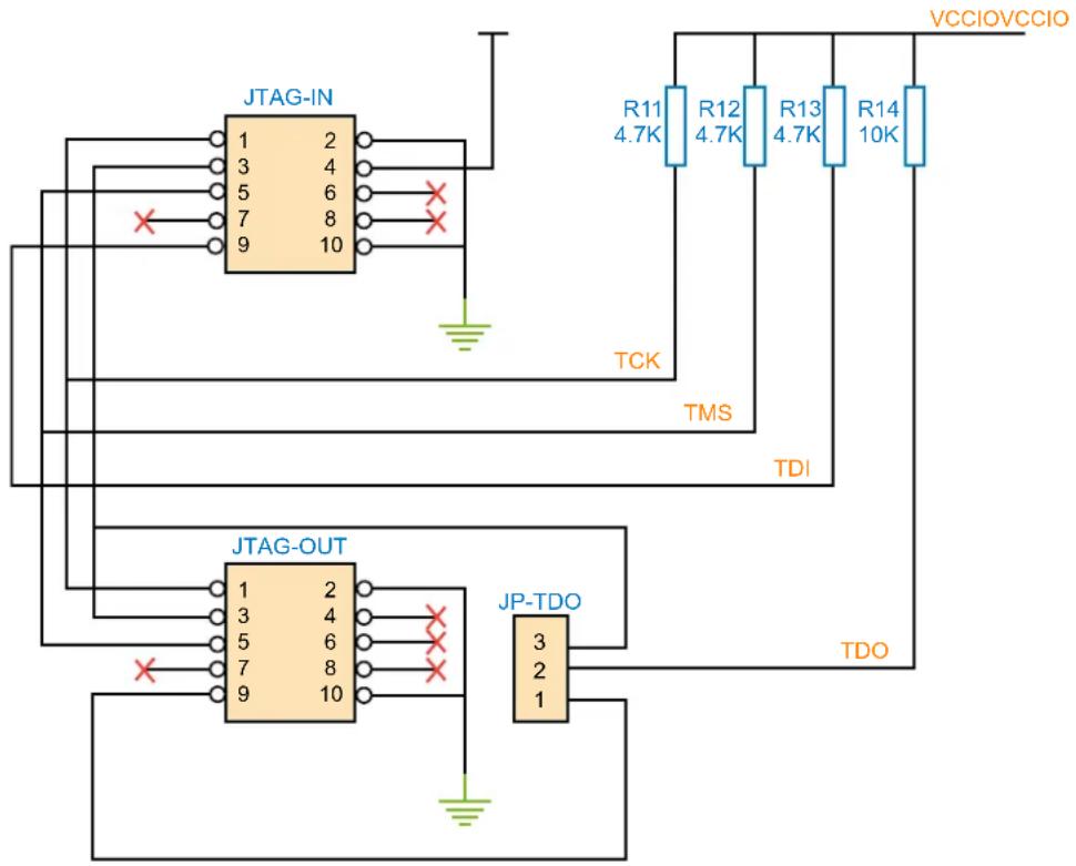
Table 7. Pin Numbers of JTAG Port Signals
| 44-pin TQFP 44-pin PLCC 84-pin PLCC | 100-pin TQFP | ||
| TDI 1 7 14 4 | |||
| TDO 32 38 71 73 | |||
| TMS 7 13 23 15 | |||
| TCK 26 32 62 62 |
The ISP algorithm is controlled by the ATMISP software, which is running on the PC. The four JTAG signals are generated and buffered by the ISP download cable before going into the ATF15xx device on the CPLD Development/Programmer board. The 10-pin JTAG Port Header pinout on the CPLD Development/Programmer board is shown in Figure 8, and the dimensions of this 10-pin male JTAG header are shown in Figure 9.
Figure 8. 10-pin JTAG Port Header Pinout
10-Pin JTAG Port Header (Top View)

Figure 9. 10-pin Male Header Dimensions

The 10-pin JTAG Port Header pinout is compatible with the ATDH1150USB and ATDH1150USB-K USB based ISP cables as well as the ATDH1150PC/VPC and ByteBlaster/MV/II LPT port based ISP cables. ATMISP v6.7 supports both the USB and LPT port based ISP cables while ATMISP v7.x and later only supports the USB port based ISP cables.
Socket Adapter Board
The ATF15xx-DK3 CPLD Development/Programmer Socket Adapter Boards (ATF15xxDK3-XXXXX) are circuit boards that interface with the ATF15xx-DK3 CPLD Development/Programmer Board. They are used in conjunction with the ATF15xx-DK3 CPLD Development/Programmer Board to evaluate or program ATF15xx ISP CPLD devices in different package types. There are four Socket Adapter Boards available for the ATF15xx-DK3 covering the 44-TQFP, 44-PLCC, 84-PLCC, and 100-TQFP package types in the ATF15xx family of CPLDs.
Each socket adapter board contains a socket for the ATF15xx device and has male headers on the bottom side, labeled JP1 and JP2. The headers on the bottom side mate with the female headers on the ATF15xx-DK3 board, labeled JP4 and JP3. The four 7-segment displays, push-button switches, JTAG port signals, oscillator, VCC INT, VCC IO, and GND on the CPLD Development/Programmer Board are connected to the ATF15xx device on the Socket Adapter Board through these two sets of connectors.
On the top of the 44-TQFP socket adapter, there are four 10-pin connectors with the same dimensions as the JTAG ISP connector. The pins of these four connectors are connected to the input and I/O pins (except the four JTAG pins) of the target CPLD device. They can be used to connect to an oscilloscope or logic analyzer to capture the activities of the input and I/O pins of the CPLD. They also can be used to connect the input and I/O pins of the CPLD to other external boards or devices for system level evaluation or testing.
Atmel ATF15xx ISP Download Cable
The ATF15xx USB ISP Download Cable connects the USB port of the PC to the 10-pin JTAG header on the CPLD Development/Programmer Board or a custom circuit board. This ISP cable also acts as a buffer to buffer the JTAG signals for the JTAG devices on the target circuit board. The status LED on the ATF15xx USB ISP Download Cable indicates whether the communication between the PC and the target JTAG devices and the JTAG operation are successful or not.
This ISP cable contains a standard B USB connector, which is connected to the USB port of a PC. The 10-pin female plug connects to the 10-pin male JTAG header on the ISP circuit board. The red color stripe on the ribbon cable indicates the orientation of pin 1 of the female plug. The 10-pin male JTAG header on the CPLD Development/Programmer Board is polarized to prevent users from inserting the female plug in the wrong orientation.
The CPLD Development/Programmer kits includes the ATF15xx USB ISP Download Cable (ATDH1150USB or ATDH1150USB-K); however, other supported ISP cables can also be used. The ATDH1150VPC, ATDH1150USB, ByteBlasterMV, and ByteBlasterII cables can be used for the ATF15xx/ASL (5V) and ATF15xxASV/ASVL (3.3V) devices, while the older ATDH1150PC and the ByteBlaster cables can be used for the ATF15xxAS/ASL (5V) only.
Figure 10 illustrates the 10-pin female header pinout for the ATF15xx ISP Download Cable. The 10-pin male header pinout on the PC board (if used for ISP) must match this pinout.
Figure 10. ATF15xx ISP Download Cable 10-pin Female Header Pinout

Note: The circuit board must supply V cc and GND to the CPLD ISP Cable through the 10-pin male header.
Figure 11. ATF15xx-D3 Development/Programmer Kit Schematic Diagram

Figure 12. 44-pin TQFP Socket Adapter Board Schematic Diagram

Figure 13. 44-pin PLCC Socket Adapter Board Schematic Diagram

Figure 14. 84-pin PLCC Socket Adapter Board Schematic Diagram

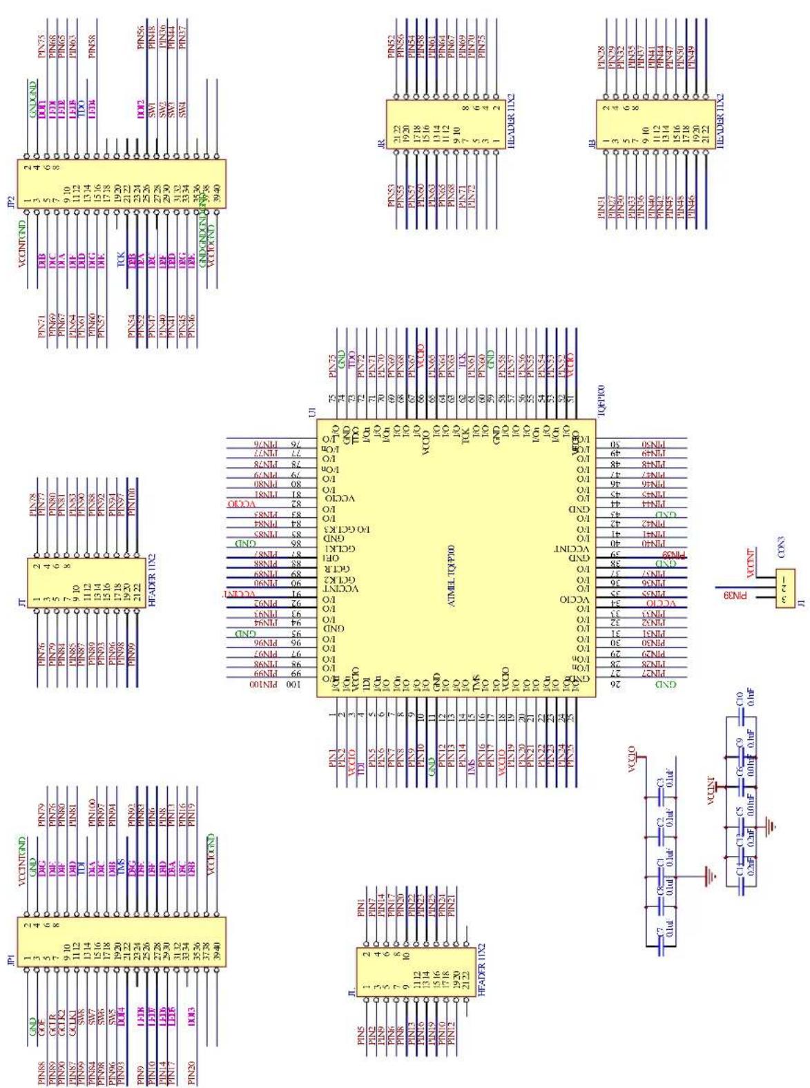
Figure 15. 100-pin TQFP Socket Adapter Board Schematic Diagram
References and Support
For additional PLD design software references and support, documentation such as help files, tutorials, application notes/briefs, and user guides are available at www.atmel.com.
Atmel ProChip Designer Software
Table 8. ProChip Designer References and Support
| ProChip Designer From the main ProChip window menu... | |
| Help Select Help > Prochip Designer Help. | |
| Tutorials Select Help > Tutorials. | |
| Known Problems and Solutions Select Help > Review KPS. | |
| Website www.atmel.com/tools/PROCHIPDESIGNERV5_0.aspx |
Atmel WinCUPL Software
Table 9. WinCUPL References and Support
| WinCUPL From the main WinCUPL window menu... | |
| Help Select Help > Contents. | |
| CUPL Programmers Reference Guide | Select Help > CUPL Programmers Reference. |
| Tutorials | Select Help > Atmel Info > Tutorial1.pdf. |
| Known Problems and Solutions | Select Help > Atmel Info > CUPL BUG.pdf. |
| Website www.atmel.com/tools/WINCUPL.aspx | |
Atmel ATMISP Software
Table 10. ATMISP References and Support
| ATMISP From the main ATMISP window menu... | |
| Help Files Select Help > ATMISP Help. | |
| Tutorials | Select Help > Quick Start Tutorial. |
| Known Problems and Solutions | Using the Windows Explorer browser, locate the ATMISP folder and open the readme.txt file with an ASCII text editor. |
| Website www.atmel.com/tools/ATMISP.aspx | |
Atmel POF2JED Conversion Software
Table 11. POF2JED References and Support
| POF2JED From the main POF2JED window menu... | |
| ATF15xx Conversion Application Brief | Select Help > Conversion Options. |
Technical Support
For technical support on any Atmel PLD related issues, contact the Atmel PLD Applications Group at:
Email pld@atmel.com
Hotline (+1)(408) 436-4333
Online Support Form www.atmel.com/design-support/
Revision History
Revision Date Description
8961A 07/2015 Initial document release.
Atmel
Enabling Unlimited Possibilities®

Atmel Corporation
1600 Technology Drive, San Jose, CA 95110 USA
T: (+1)(408) 441.0311
F: (+1)(408) 436.4200
| www.atmel.com
© 2015 Atmel Corporation. / Rev.: Atmel-8961A-CPLD-ATF15xx-DK3-U-Development-Kit-UserGuide_072015.
Atmel ® , Atmel logo and combinations thereof, Enabling Unlimited Possibilities, and others are registered trademarks or trademarks of Atmel Corporation in U.S. and other countries. Windows ® is a registered trademark of Microsoft Corporation in U.S. and or other countries. Other terms and product names may be trademarks of others.
DISCLAIMER: The information in this document is provided in connection with Atmel products. No license, express or implied, by estoppel or otherwise, to any intellectual property right is granted by this document or in connection with the sale of Atmel products. EXCEPT AS SET FORTH IN THE ATMEL TERMS AND CONDITIONS OF SALES LOCATED ON THE ATMEL WEBSITE, ATMEL ASSUMES NO LIABILITY WHATSOEVER AND DISCLAIMS ANY EXPRESS, IMPLIED OR STATUTORY WARRANTY RELATING TO ITS PRODUCTS INCLUDING, BUT NOT LIMITED TO, THE IMPLIED WARRANTY OF MERCHANTABILITY, FITNESS FOR A PARTICULAR PURPOSE, OR NON-INFRINGEMENT. IN NO EVENT SHALL ATMEL BE LIABLE FOR ANY DIRECT, INDIRECT, CONSEQUENTIAL, PUNITIVE, SPECIAL OR INCIDENTAL DAMAGES (INCLUDING, WITHOUT LIMITATION, DAMAGES FOR LOSS AND PROFITS, BUSINESS INTERRUPTION, OR LOSS OF INFORMATION) ARISING OUT OF THE USE OR INABILITY TO USE THIS DOCUMENT, EVEN IF ATMEL HAS BEEN ADVISED OF THE POSSIBILITY OF SUCH DAMAGES. Atmel makes no representations or warranties with respect to the accuracy or completeness of the contents of this document and reserves the right to make changes to specifications and products descriptions at any time without notice. Atmel does not make any commitment to update the information contained herein. Unless specifically provided otherwise, Atmel products are not suitable for, and shall not be used in, automotive applications. Atmel products are not intended, authorized, or warranted for use as components in applications intended to support or sustain life.
SAFETY-CRITICAL, MILITARY, AND AUTOMOTIVE APPLICATIONS DISCLAIMER: Atmel products are not designed for and will not be used in connection with any applications where the failure of such products would reasonably be expected to result in significant personal injury or death ("Safety-Critical Applications") without an Atmel officer's specific written consent. Safety-Critical Applications include, without limitation, life support devices and systems, equipment or systems for the operation of nuclear facilities and weapons systems. Atmel products are not designed nor intended for use in military or aerospace applications or environments unless specifically designated by Atmel as military-grade. Atmel products are not designed nor intended for use in automotive applications unless specifically designated by Atmel as automotive-grade.



- KIT CONTENTS
- DEVICE SUPPORT
- TABLE OF CONTENTS
- KIT FEATURES 3
- SYSTEM REQUIREMENTS 3
- ORDERING INFORMATION....4
- HARDWARE DESCRIPTION 4
- SCHEMATIC DIAGRAMS 15
- REFERENCES AND SUPPORT 20
- TECHNICAL SUPPORT 21
- REVISION HISTORY 21
- KIT FEATURES
- CPLD DEVELOPMENT/PROGRAMMER BOARD
- LOGIC DOUBLING CPLDS
- ATF15XX ISP DOWNLOAD CABLE
- PLD DEVELOPMENT SOFTWARE
- SYSTEM REQUIREMENTS
- ORDERING INFORMATION
- HARDWARE DESCRIPTION
- 7-SEGMENT DISPLAYS WITH SELECTABLE JUMPERS
- LEDS WITH SELECTABLE JUMPERS
- PUSH-BUTTON SWITCHES WITH SELECTABLE JUMPERS FOR I/O PINS
- PUSH-BUTTON SWITCHES WITH SELECTABLE JUMPERS FOR GCLR AND OE1 PINS
- 2MHZ OSCILLATOR AND CLOCK SELECTION JUMPER
- VCCIO AND VCCINT VOLTAGE SELECTION JUMPERS AND LEDS
- ICCIO AND ICCINT JUMPERS
- VOLTAGE REGULATORS
- POWER SUPPLY SWITCH AND POWER LED
- POWER SUPPLY JACK AND POWER SUPPLY HEADER
- JTAG ISP CONNECTOR AND TDO SELECTION JUMPER
- SOCKET ADAPTER BOARD
- ATMEL ATF15XX ISP DOWNLOAD CABLE
- REFERENCES AND SUPPORT
- ATMEL PROCHIP DESIGNER SOFTWARE
- ATMEL WINCUPL SOFTWARE
- ATMEL ATMISP SOFTWARE
- ATMEL POF2JED CONVERSION SOFTWARE
- TECHNICAL SUPPORT
- REVISION HISTORY
Brand : Microchip
Model : ATF15xx-DK3-U
Category : Electronic development kit