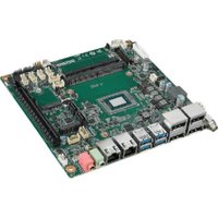
AIMB-2210 - Motherboard Advantech - Free user manual and instructions
Find the device manual for free AIMB-2210 Advantech in PDF.


| Product Type | Industrial Motherboard |
| Brand | Advantech |
| Model | AIMB-2210 |
| Form Factor | Mini-ITX (170 mm x 170 mm) |
| Dimensions | 170 mm x 170 mm |
| Weight | Approx. 0.5 kg |
| Processor Support | Intel Core i7/i5/i3 or Celeron (8th/9th Gen) |
| Chipset | Intel H310 |
| Memory | 2 x DDR4 SO-DIMM, up to 32 GB |
| Expansion Slots | 1 x PCIe x16, 1 x PCIe x4, 1 x M.2 |
| Storage Interfaces | 2 x SATA III, 1 x M.2 (SATA/PCIe) |
| Ethernet | 2 x Gigabit LAN (Intel i210) |
| USB Ports | 4 x USB 3.0, 2 x USB 2.0 |
| Display Output | VGA, HDMI, LVDS (dual display support) |
| Audio | Realtek ALC888S, 5.1 channel |
| Power Input | 12V DC or ATX (24-pin) |
| Power Consumption | Typical 60W |
| Operating Temperature | 0°C to 60°C |
| OS Support | Windows 10, Linux |
| Certifications | CE, FCC Class A |
| Warranty | 2 years (standard) |
| Special Features | Watchdog timer, TPM 2.0, industrial temperature range |
Frequently Asked Questions - AIMB-2210 Advantech
User questions about AIMB-2210 Advantech
0 question about this device. Answer the ones you know or ask your own.
Ask a new question about this device
Download the instructions for your Motherboard in PDF format for free! Find your manual AIMB-2210 - Advantech and take your electronic device back in hand. On this page are published all the documents necessary for the use of your device. AIMB-2210 by Advantech.
USER MANUAL AIMB-2210 Advantech
AIMB-2210
Mini-ITX Motherboard with AMD Ryzen™ Embedded 8000 Series Processor
Copyright
The documentation and the software included with this product are copyrighted 2025 by Advantech Co., Ltd. All rights are reserved. Advantech Co., Ltd. reserves the right to make improvements in the products described in this manual at any time without notice. No part of this manual may be reproduced, copied, translated, or transmitted in any form or by any means without the prior written permission of Advantech Co., Ltd. The information provided in this manual is intended to be accurate and reliable. However, Advantech Co., Ltd. assumes no responsibility for its use, nor for any infringements of the rights of third parties that may result from its use.
Acknowledgments
IBM and PC are trademarks of International Business Machines Corporation.
Intel® Core™ i9/i7/i5/i3, Pentium®, and Celeron® are trademarks of the Intel Corporation.
All other product names or trademarks are properties of their respective owners.
Product Warranty (2 Years)
Advantech warrants the original purchaser that each of its products will be free from defects in materials and workmanship for two years from the date of purchase.
This warranty does not apply to any products that have been repaired or altered by persons other than repair personnel authorized by Advantech, or products that have been subject to misuse, abuse, accident, or improper installation. Advantech assumes no liability under the terms of this warranty as a consequence of such events.
Because of Advantech's high quality-control standards and rigorous testing, most customers never need to use our repair service. If an Advantech product is defective, it will be repaired or replaced free of charge during the warranty period. For out-of-warranty repairs, customers will be billed according to the cost of replacement materials, service time, and freight. Please consult your dealer for more details.
If you believe your product to be defective, follow the steps outlined below.
-
Collect all the information about the problem encountered. (For example, CPU speed, Advantech products used, other hardware and software used, etc.) Note anything abnormal and list any onscreen messages displayed when the problem occurs.
-
Call your dealer and describe the problem. Please have your manual, product, and any helpful information readily available.
-
If your product is diagnosed as defective, obtain a return merchandise authorization (RMA) number from your dealer. This allows us to process your return more quickly.
-
Carefully pack the defective product, a completed Repair and Replacement Order Card, and a proof of purchase date (such as a photocopy of your sales receipt) into a shippable container. Products returned without a proof of purchase date are not eligible for warranty service.
-
Write the RMA number clearly on the outside of the package and ship the package prepaid to your dealer.
Part No. 20060221000 Edition 1
Printed in China May 2025
A Message to the Customer
Advantech Customer Services
Each and every Advantech product is built to the most exacting specifications to ensure reliable performance in the harsh and demanding conditions typical of industrial environments. Whether your new Advantech equipment is destined for the laboratory or the factory floor, you can be assured that your product will provide the reliability and ease of operation for which the name Advantech has come to be known. Your satisfaction is our primary concern. Here is a guide to Advantech's customer services. To ensure you get the full benefit of our services, please follow the instructions below carefully.
Technical Support
We want you to get the maximum performance from your products. If you run into technical difficulties, we are here to help. For the most frequently asked questions, you can easily find answers in your product documentation. These answers are normally a lot more detailed than the ones we can give over the phone.
Please consult this manual first. If you still cannot find the answer, gather all the information or questions that apply to your problem, and with the product close at hand, call your dealer. Our dealers are well trained and ready to give you the support you need to get the most from your Advantech products. In fact, most problems reported are minor and are able to be easily solved over the phone.
In addition, free technical support is available from Advantech engineers every business day. We are always ready to give advice on application requirements or specific information on the installation and operation of any of our products.
Declaration of Conformity
FCC Class B
This equipment has been tested and found to comply with the limits for a Class B digital device, pursuant to part 15 of the FCC Rules. These limits are designed to provide reasonable protection against harmful interference in a residential installation. This equipment generates, uses, and can radiate radio frequency energy and, if not installed and used in accordance with the instruction manual, may cause harmful interference to radio communications. However, there is no guarantee that interference will not occur in a particular installation. If this equipment does cause harmful interference to radio or television reception, which can be determined by turning the equipment off and on, the user is encouraged to try to correct the interference by one or more of the following measures:
Reorient or relocate the receiving antenna.
Increase the separation between the equipment and receiver.
Connect the equipment into an outlet on a circuit different from that to which the receiver is connected.
Consult the dealer or an experienced radio/TV technician for assistance.
Memory Compatibility
| Category Speed Capacity Vendor ADVANTECH P/N ECC | ||
| DDR5 5600 8GB Advantech SQR-SD5N8G5K6HNGAG N | ||
| DDR5 5600 16GB | Advantech SQR-SD5N16G5K6HNAG | N |
| DDR5 5600 32GB | Advantech SQR-SD5N32G5K6HNAG | N |
| DDR5 4800 32GB | Advantech SQR-SD5N32G4K8HNAG | N |
| DDR5 4800 32GB | Advantech AQD-SD5V32GN48-SB | N |
| DDR5 4800 16GB | Advantech AQD-SD5V16GN48-SB | N |
| DDR5 5600 16GB | Advantech AQD-SD5V16GN56-SB | N |
| DDR5 5600 32GB | Advantech AQD-SD5V32GN56-SB | N |
| DDR5 5600 48GB | Advantech SQR-SD5N48G5K6M | N |
| DDR5 4800 32GB | Advantech SQR-SD5N32G4K8SEBB ECC | |
| DDR5 4800 16GB | Advantech SQR-SD5N16G4K8SEBB ECC | |
| DDR5 5600 32GB | Advantech SQR-SD5N32G5K6SEPB ECC | |
| DDR5 4800 16GB | Advantech AQD-SD5V16GE48-SB | ECC |
| DDR5 4800 32GB | Advantech AQD-SD5V32GE48-SB | ECC |
| DDR5 5600 16GB | Advantech AQD-SD5V16GE56-SB | ECC |
| DDR5 5600 32GB | Advantech AQD-SD5V32GE56-SB | ECC |
Ordering Information
| P/N | CPU | TDP | LVDS/eDP | DP | DDR5 | GbE | COM | SATAIII | USB 3.2 | USB 2.0 | M.2 E-Key | M.2 M-Key | PCIe x16 | TPM | AMP |
| AIMB-2210R-00A1 | 8845HS | 45W | (1)/(1) | 4* | 2 | 2** | 6 | 2 | 4 | 4 | 1 | 2 | 1 | 1 | (1) |
| AIMB-2210R-01A1 | 8840U | 28W | (1)/(1) | 4* | 2 | 2** | 6 | 2 | 4 | 4 | 1 | 2 | 1 | 1 | (1) |
| AIMB-2210R-02A1 | 8645HS | 45W | (1)/(1) | 4* | 2 | 2** | 6 | 2 | 4 | 4 | 1 | 2 | 1 | 1 | (1) |
| AIMB-2210R-03A1 | 8640U | 28W | (1)/(1) | 4* | 2 | 2** | 6 | 2 | 2+(2) | 4*** | 1 | 2 | 1 | 1 | (1) |
() Supported by BOM option
*DP1 colay with eDP/LVDS, 4 independent displays, LVDS or eDP or DP1 + DP2/DP3/DP4
**LAN default 1 x GbE x2; supports 2.5 GbE by option
***AIMB-2210R-03A1:
Default (rear) 2 x USB 3.2 Gen2x1 + 2 x USB 2.0 & (internal) 2 x USB 2.0
Optional (rear) 4 x USB 3.2 Gen2x1 + (internal) 4 x USB 2.0
Initial Inspection
Before you begin installing your motherboard, please make sure that the following materials have been shipped:
1 x AIMB-2210 Motherboard
1 x SATA HDD cable
■ 1 x SATA power cable
■ 1 x serial port cable
■ 1 x I/O port bracket
1 x Startup Manual
1 x Warranty Card
■ 3 x screws (M3x4L)
If any of these items are missing or damaged, contact your distributor or sales representative immediately. We have carefully inspected the AIMB-2210 mechanically and electrically before shipment. It should be free of marks and scratches and in perfect working order upon receipt. As you unpack the AIMB-2210, check it for signs of shipping damage. (For example, damaged box, scratches, dents, etc.) If it is damaged or it fails to meet the specifications, notify our service department or your local sales representative immediately. Also notify the carrier. Retain the shipping carton and packing material for inspection by the carrier. After inspection, we will make arrangements to repair or replace the unit.
Contents
Chapter 1 General Introduction ......1
1.1 Introduction ...... 2
1.2 Features 2
1.3 Specifications 2
1.3.1 System 2
1.3.2 Memory 2
1.3.3 Input/Output 2
1.3.4 Graphics.... 3
1.3.5 Ethernet LAN 3
1.3.6 Industrial Features 3
1.3.7 Mechanical and Environmental Specifications.... 3
1.4 Jumpers and Connectors 4
Table 1.1: I/O Connector 4
Table 1.2: Box Header....4
Table 1.3: Pin Header....5
Table 1.4: Jumper Settings....5
1.5 Board Layout: Jumper and Connector Locations....6
Figure 1.1 Jumper and Connector Locations (Top Side)....6
Figure 1.2 Jumper and Connector Locations (Bottom Side)...... 7
1.6 AIMB-2210 Board Diagram 7
Figure 1.3 AIMB-2210 Board Diagram 7
1.7 Safety Precautions 8
1.8 Jumper Settings 8
1.8.1 How to Set Jumpers.... 8
1.8.2 EDP Panel / LVDS Panel Voltage Selection (JEDP1_LVDS1)..... 9
Table 1.5: JEDP1_LVDS1 9
1.8.3 PWRBTN#/RESET# / HDD LED / Internal Buzzer / External Speaker Header (JFP1) 9
Table 1.6: JFP1 9
1.8.4 COM1_RI# Pin RI#/5V/12V Selection (JSETCOM1_V1)....9
Table 1.7: JSETCOM1_V1 9
1.8.5 COM4_RI# Pin RI#/5V/12V Selection (JSETCOM4_V1).... 10
Table 1.8: JSETCOM4 V1 10
1.8.6 AT/ATX Mode Selection (PSON1) 10
Table 1.9: PSON1 10
1.8.7 Case Open State (NC/NO) Setting Pin Header (JCASEOP_SW1) 10
Table 1.10:JCASEOP SW1 10
1.8.8 MOS Clear Jumper (JCMOS1) 11
Table 1.11:JCMOS1 1
1.8.9 COM3 CCTALK Voltage Selection Header (JCCT_VCON1).... 11
Chapter 2 Connecting Peripherals ....13
2.1 Introduction 14
2.2 I/O Connector....14
2.2.1 Dual DisplayPort (DP12).... 14
Table 2.1: Dual DisplayPort (DP12) 14
2.2.2 Dual DisplayPort (DP34).... 15
Table 2.2: Dual DisplayPort (DP34) 15
2.2.3 USB 3.1 Stack Connector * 2 Ports (USB3_12) ...... 16
Table 2.3: USB 3.1 Stack Connector * 2 Ports (USB3_12)..... 16
2.2.4 USB 3.1 Stack Connector * 2 Ports (USB_34) ...... 17
Table 2.4: USB 3.1 Stack Connector * 2 Ports (USB_34)..... 17
2.2.5 RJ-45 Single LAN Port (LAN1) 18
Table 2.5: RJ-45 Single LAN Port (LAN1).... 18
2.2.6 RJ-45 Single LAN Port (LAN2) 19
Table 2.6: RJ-45 Single LAN Port (LAN2).... 19
2.2.7 M.2 E-Key Connector (M2_E1).... 20
Table 2.7: M.2 E-Key Connector (M2_E1) 20
2.2.8 M.2 M-Key Connector (M2_M1) 21
Table 2.8: M.2 M-Key Connector (M2_M1) ...... 21
2.2.9 M.2 M-Key Connector (M2_M2) 22
Table 2.9: M.2 M-Key Connector (M2_M2) ...... 22
2.2.10 12V Power Supply Connector (DCIN1) 23
Table 2.10:12V Power Supply Connector (DCIN1) ...... 23
2.2.11 SATA Connector (SATA1) 24
Table 2.11:SATA Connector (SATA1).... 24
2.2.12 SATA Connector (SATA2) 24
Table 2.12:SATA Connector (SATA2).... 24
2.2.13 PCIe x16 Connector (PCIEX16 1) 25
Table 2.13:PCIe x16 Connector (PCIEX16_1).... 25
2.2.14 HD Analog Audio Interface Line-Out (AUDIO1)...... 27
Table 2.14:HD Analog Audio Interface Line-Out (AUDIO1) ..... 27
2.2.15 HD Analog Audio Interface Mic-In (AUDIO2).... 27
Table 2.15:HD Analog Audio Interface Mic-In (AUDIO2) ...... 27
2.2.16 DDR5 SODIMM Socket A1 (DIMMA1) 27
2.2.17 DDR5 SODIMM Socket B1 (DIMMB1) 27
2.3 Box Header 28
2.3.1 EDP Connector / LVDS Connector (EDP1_LVDS1).... 28
Table 2.16:LVDS1 28
Table 2.17:EDP1 29
2.3.2 Internal USB 2.0 Connector * 2 Ports (USB56) ...... 29
Table 2.18:Internal USB 2.0 Connector * 2 Ports (USB56)...... 29
2.3.3 Internal USB 2.0 Connector * 2 Ports (USB78) 30
Table 2.19:Internal USB 2.0 Connector * 2 Ports (USB78)...... 30
2.3.4 COM1 Connector (COM1) 30
Table 2.20:COM1 Connector (COM1).... 30
2.3.5 COM2 Connector (COM2) 31
Table 2.21:COM2 Connector (COM2).... 31
2.3.6 COM3 Connector (COM3) 31
Table 2.22:COM3 Connector (COM3).... 31
2.3.7 COM4 Connector (COM4) 32
Table 2.23:COM4 Connector (COM4).... 32
2.3.8 COM4 Connector (COM5) 32
Table 2.24:COM4 Connector (COM5).... 32
2.3.9 COM4 Connector (COM6) 33
Table 2.25:COM4 Connector (COM6).... 33
2.3.10 CMOS Battery Connector (BAT1).... 3
Table 2.26:CMOS Battery Connector (BAT1) 33
2.3.11 EDP/LVDS Backlight Inverter Power Connector (INV1) 3
Table 2.27:EDP/LVDS Backlight Inverter Power Connector (INV1) 34
2.3.12 ATX 4-Pin Power Connector (ATX12V1).... 34
Table 2.28:ATX 4-Pin Power Connector (ATX12V1) 34
2.3.13 ATX 5V/PSON Connector (ATX_5VSB1) 35
Table 2.29:ATX 5V/PSON Connector (ATX_5VSB1).... 35
2.3.14 SATA Power Connector (SATA_PWR1) 35
Table 2.30:SATA Power Connector (SATA_PWR1) ...... 35
2.3.15 SATA Power Connector (SATA_PWR2).... 36
Table 2.31:SATA Power Connector (SATA_PWR2) ...... 36
2.4 Pin Header 36
2.4.1 Power LED Pin Header (JFP2) 36
Table 2.32:Power LED Pin Header (JFP2).... 36
2.4.2 SPI BIOS Flash Socket1 (SPI1).... 37
Table 2.33:SPI BIOS Flash Socket1 (SPI1) ...... 37
2.4.3 SPI BIOS Debug Header (SPI_CN1).... 37
Table 2.34:SPI BIOS Debug Header (SPI_CN1) ...... 37
2.4.4 8-Bit General Purpose I/O Pin Header (GPIO1) 38
Table 2.35:8-Bit General Purpose I/O Pin Header (GPIO1)..... 38
2.4.5 8-Bit General Purpose I/O Pin Header (GPIO2) 38
Table 2.36:8-Bit General Purpose I/O Pin Header (GPIO2)..... 38
2.4.6 CPU FAN Connector (CPUFAN1) 38
Table 2.37:CPU FAN Connector (CPUFAN1) 38
2.4.7 System Fan Connector (SYSFAN1) 39
Table 2.38:System Fan Connector (SYSFAN1) 39
2.4.8 Case Open Connector (JCASE1) 39
Table 2.39:Case Open Connector (JCASE1).... 39
2.4.9 VCORE Programming Header (VR_PMB1).... 39
Table 2.40:VCORE Programming Header (VR_PMB1) ...... 39
2.4.10 HD Digital Audio Interface S/PDIF Out (SPDIF1) 4
Table 2.41: HD Digital Audio Interface S/PDIF Out (SPDIF1)..... 40
2.4.11 Audio Amplifier Output Pin Header (AMP1).... 40
Table 2.42:Audio Amplifier Output Pin Header (AMP1) ...... 40
2.4.12 HD Analog Audio Interface Front Panel (FPAUD1) 4
Table 2.43:HD Analog Audio Interface Front Panel (FPAUD1).. 41
2.4.13 LED Port 80 Connector (LED_P80) 4
Table 2.44:LED Port 80 Connector (LED_P80).... 41
2.5 Jumper Settings 42
2.5.1 COM1 RI# Selection Pin Header (JSETCOM1_V1) 42
Table 2.45:COM1 RI# Selection Pin Header (JSETCOM1_V1). 42
2.5.2 COM4 RI# Selection Pin Header (JSETCOM4_V1) 42
Table 2.46:COM4 RI# Selection Pin Header (JSETCOM4_V1). 42
2.5.5 PWRBTN# / RESET# / HDD LED / Serial Bus from HW Monitor IC
/ Internal Buzzer / External Speaker Header (JFP1)...... 43
Table 2.49: PWRBTN# / RESET#/HDD LED / Serial Bus from HW Monitor IC / Internal Buzzer / External Speaker Header (JFP1).... 43
2.5.6 Case Open Signal Reverse Header (JCASEOP_SW1).... 44
Table 2.50: Case Open Signal Reverse Header (JCASEOP_SW1) 44
2.5.7 CMOS Reset Header (JCMOS1) 44
Table 2.51:CMOS Reset Header (JCMOS1).... 44
2.5.8 AT/ATX Mode Selection (PSON1) 44
Table 2.52:AT/ATX Mode Selection (PSON1).... 44
Chapter 3 BIOS Operation......47
3.1 Introduction ...... 48
3.2 BIOS Setup 48
Table 3.1: Control Keys.... 48
3.2.1 Main Menu 49
3.2.2 Advanced BIOS Features 50
3.2.3 Chipset Configuration Setting 69
3.2.4 Security....72
3.2.5 Boot Settings 73
3.2.6 Save & Exit Configuration.... 74
Chapter 4 Software Introduction & Service ..... 75
4.1 Introduction ...... 76
4.2 Value-Added Software Services 76
4.2.1 Software API....76
4.2.2 Software Utility....78
Chapter 5 Chipset Software Installation Utility 79
5.1 Before You Begin....80
5.2 Introduction 80
Chapter 6 LAN Configuration 81
6.1 Introduction 82
6.2 Features....82
6.3 Installation....82
6.4 Windows® 11 Driver Setup (Realtek 8111G) 82
Chapter 1
General Introduction
1.1 Introduction
The AIMB-2210 Mini-ITX motherboard is powered by the AMD Ryzen™ Embedded 8000 Series Processor, delivering high-performance computing and energy efficiency for industrial applications. It supports Ryzen 7 Pro and Ryzen 5 Pro CPUs, and up to 96GB of single-channel DDR5 5600MT/s ECC memory via two SODIMM slots.
For connectivity, the AIMB-2210 includes 6 COM ports, 4 USB 3.2 Gen2x1 ports, 4 USB 2.0 ports, and dual Ethernet ports with support for 1 GbE and optional 2.5 GbE.
Storage and expansion options include 2 SATA III ports and 3 M.2 slots—two M-Key slots for NVMe SSDs or Hailo AI modules, and one E-Key slot for wireless modules such as Wi-Fi or Bluetooth.
Graphics are powered by integrated AMD RDNA 3 Radeon Graphics, supporting up to four independent displays through 4 DisplayPort++ outputs. It also supports mixed configurations with DP and LVDS or eDP, with resolutions up to 4K.
1.2 Features
I/O Expansion: 6 x serial ports, 4 x USB 3.2 Gen2x1 ports, 4 x USB 2.0 ports, 2 x SATA III connectors, 2 x M.2 M-Key slots, 1 x M.2 E-Key, and 2 x 1 GbE LAN ports.
■ Mini-ITX Form Factor: AIMB-2210 is a Mini-ITX motherboard.
Wide selection of storage devices: SATA HDD, dual M-Key slots for NVMe SSDs or Hailo AI modules and an E-Key slot for wireless connectivity such as Wi-Fi or Bluetooth.
■ Optimized Integrated Graphics: AMD RDNA 3 Radeon Graphics.
1.3 Specifications
1.3.1 System
CPU: Supports AMD Ryzen™ Embedded 8000 Series Processor
BIOS: AMI EFI 256 Mbit SPI BIOS.
■ SATA hard disk drive interface:
- 2 x on-board SATA connectors with data transmission rates up to 6 GB/s
- 2 x M.2 M-Key slots (2242/2280), supporting NVMe SSDs or Hailo AI modules
- 1 x M.2 E-Key slot (2230), supporting Wi-Fi/BT
1.3.2 Memory
■ RAM: 2 x 262-pin SODIMM sockets supporting dual-channel DDR5 5600MT/s SDRAM, up to 96GB Max.
1.3.3 Input/Output
■ Serial ports: 6 serial ports
- COM1: Support RS-232 (RI Power 5V/12V)
- COM2 and 5: Support RS-232/422/485, by BOM option
- COM3: Support RS-232 (CCTalk by BOM option)
- COM4: Support RS-232 (TTL, RI Power 5V/12V by BOM option)
- COM6: Support RS-232
USB ports: Supports up to 4 x USB 3.2 Gen2x1 and 4 x USB 2.0
■ GPIO connector: 16-bit general purpose Input/Output.
1.3.4 Graphics
■ Controller: AMD RDNA 3 Radeon Graphics
LVDS or eDP: Supports 1 x LVDS maximum resolution up to 1920 x 1080 @60Hz, colay with DP1 or 1 x eDP maximum resolution up to 3840 x 2160 @120Hz 8bpc.
■ DP: Supports 4 x DP++ maximum resolution up to 3840 x 2160 @120Hz.
1.3.5 Ethernet LAN
■ Supports dual 10/100/1000/2500 Mbps Ethernet ports
Controller:
– GbE LAN1: RTL8111K 1GbE (co-design RTL8125BG 2.5 GbE)
– GbE LAN2: RTL8111K 1GbE (co-design RTL8125BG 2.5 GbE)
1.3.6 Industrial Features
- Watchdog timer: The watchdog timer can generate a system reset. It is programmable, with each unit equal to one second or one minute (255 levels).
1.3.7 Mechanical and Environmental Specifications
Operating temperature: 0 \~ 60°C (32 \~ 140°F), depends on CPU speed and cooler solution.
■ Storage temperature: -40 \~ 85°C (-40 \~ 185°F).
■ Humidity: 5 \~ 95% non-condensing.
■ Power supply voltage: 12-24V (tolerance: -10%/+ 20%)
Power consumption: Boost 86.9W; Typical 73.9W (configuration: AMD Ryzen™ 7 Pro 8845HS, 2pcs 48 GB DDR5 5600 MT/s)
■ Board size: 170 x 230 mm (6.69" x 9.06")
■ Board weight: 1.0 kg
1.4 Jumpers and Connectors
Connectors on the AIMB-2210 motherboard link it to devices such as hard disk drives and a keyboard. In addition, the board has a number of jumpers used to configure the system for your application.
The tables below list the function of each of the board jumpers and connectors. Later sections in this chapter give instructions on setting jumpers. Chapter 2 gives instructions for connecting external devices to your motherboard.
Table 1.1: I/O Connector
| Description Part Reference | |
| 1 DUAL DisplayPort DP12 | |
| 2 DUAL DisplayPort DP34 | |
| 3 USB 3.1 stack connector * 2 ports USB3_12 | |
| 4 USB 3.1 stack connector * 2 ports USB_34 | |
| 5 RJ-45 Single LAN port LAN1 | |
| 6 RJ-45 Single LAN port LAN2 | |
| 7 M.2 E-Key Connector M2_E1 | |
| 8 M.2 M-Key Connector M2_M1 | |
| 9 M.2 M-Key Connector M2_M2 | |
| 10 12V ~ 24V Power Supply Connector DCIN1 | |
| 11 SATA Connector | SATA1 |
| 12 SATA Connector | SATA2 |
| 13 PCIe x16 Connector | PCIEX16_1 |
| 14 HD Analog Audio Interface Line-Out | AUDIO1 |
| 15 HD Analog Audio Interface Mic-In | AUDIO2 |
| 16 DDR5 SODIMM Socket A1 | DIMMA1 |
| 17 DDR5 SODIMM Socket B1 DIMMB1 | |
Table 1.2: Box Header
| Description Part Reference | |
| 1 EDP Connector / LVDS Connector | EDP1_LVDS1 |
| 2 Internal USB 2.0 Connector * 2 ports | USB56 |
| 3 Internal USB 2.0 Connector * 2 ports | USB78 |
| 4 COM1 Connector | COM1 |
| 5 COM2 Connector | COM2 |
| 6 COM3 Connector | COM3 |
| 7 COM4 Connector | COM4 |
| 8 COM5 Connector | COM5 |
| 9 COM6 Connector | COM6 |
| 10 CMOS battery Connector | BAT1 |
| 11 EDP/LVDS Backlight Inverter Power Connector | INV1 |
| 12 ATX 4-Pin Power Connector (180D) | ATX12V1 |
| 13 ATX 5V/PSON Connector | ATX_5VSB1 |
| 14 SATA Power Connector | SATA_PWR1 |
| 15 SATA Power Connector | SATA_PWR2 |
Table 1.3: Pin Header
| Description Part Reference | |
| 1 Power LED pin header JFP2 | |
| 2 SPI BIOS flash socket SPI1 | |
| 3 SPI BIOS Debug header SPI_CN1 | |
| 4 8-bit General Purpose I/O pin header GPIO1 | |
| 5 8-bit General Purpose I/O pin header GPIO2 | |
| 6 CPU FAN Connector CPUFAN1 | |
| 7 System Fan Connector SYSFAN1 | |
| 8 Case Open Connector JCASE1 | |
| 9 VCORE Programming Header VR_PMB1 | |
| 10 HD Digital Audio Interface S/PDIF Out SPDIF1 | |
| 11 Audio Amplifier output pin header | AMP1 |
| 12 HD Analog Audio Interface Front Panel | FPAUD1 |
| 13 LED port 80 connector | LED_P80 |
Table 1.4: Jumper Settings
| Description | Part Reference | |
| 1 COM1 RI# selection pin header | JSETCOM1_V1 | |
| 2 COM4 RI# selection pin header | JSETCOM4_V1 | |
| 3 COM3 CCTALK Voltage select Header | JCCT_VCON1 | |
| 4 | EDP Panel/LVDS Panel Voltage Selection | JEDP1_LVDS1 |
| 5 | PWRBTN#/ RESET#/ HDD LED / Serial bus from HW monitor IC / Internal Buzzer / External Speaker header | JFP1 |
| 6 Case Open signal reverse header | JCASEOP_SW1 | |
| 7 CMOS reset header | JCMOS1 | |
| 8 AT/ATX Mode selection | PSON1 | |
| 9 VESA & JEIDA support select | JLVDS_VCON1 | |
1.5 Board Layout: Jumper and Connector Locations
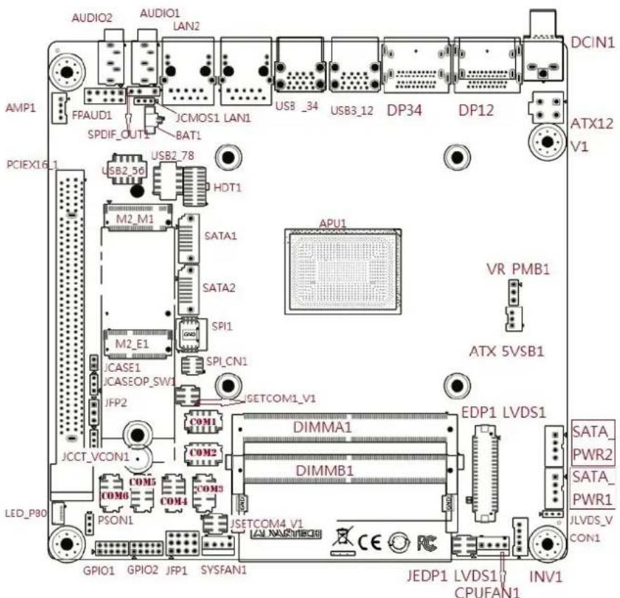
Figure 1.1 Jumper and Connector Locations (Top Side)
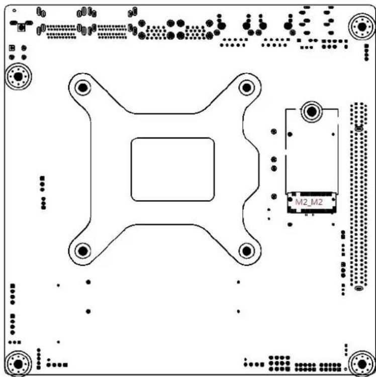
Figure 1.2 Jumper and Connector Locations (Bottom Side)
1.6 AIMB-2210 Board Diagram
![graph LR A["DP4"] <--> B["AIMB-2210 Ryzen Embedded 8000"] C["DP3"] <--> B D["DP2"] <--> B E["DP1"] <--> B F["LVDS/eDP"] <--> G["CH7513A"] H["LAN1"] <--> I["RTL8111K (co-design RTL8125BG)"] J["LAN2"] <--> K["RTL8111K (co-design RTL8125BG)"] L["2 x USB 3.2 Gen2x1"] <--> M["PCIe x1 Gen3"] N["2 x USB3.2…](/content/2026/07/1486455/images/ccc0ba1079cf81685d3774484ef97e2d9f9e79bdaea194d13fc38c65b9750b89.jpg)
Figure 1.3 AIMB-2210 Board Diagram
1.7 Safety Precautions
Warning!

Always completely disconnect the power cord from the chassis before performing any hardware work. Do not make connections while the power is on. Sensitive electronic components can be damaged by sudden power surges. Only experienced electronics personnel should open the PC chassis.
Caution!

Always ground yourself to remove any static charge before touching the motherboard. Modern electronic devices are very sensitive to electrostatic discharges. As a safety precaution, use a grounding wrist strap at all times. Place all electronic components on a static-dissipative surface or in a static-shielded bag when they are not in the chassis.
Caution!

The computer is provided with a battery-powered real-time clock circuit. There is a danger of explosion if the battery is incorrectly replaced. Replace only with the same or equivalent type recommended by the manufacturer. Discard used batteries according to the manufacturer's instructions.
Caution!

There is danger of a new battery exploding if it is incorrectly installed. Do not attempt to recharge, force open, or heat the battery. Replace the battery only with the same or equivalent type recommended by the manufacturer. Discard used batteries according to the manufacturer's instructions.
1.8 Jumper Settings
This section provides instructions on how to configure your motherboard by setting the jumpers. It also includes the motherboard's default settings and your options for each jumper.
1.8.1 How to Set Jumpers
You can configure your motherboard to match the needs of your application by setting the jumpers. A jumper is a metal bridge that closes an electrical circuit. It consists of two metal pins and a small metal clip (often protected by a plastic cover) that slides over the pins to connect them. To “close” (or turn ON) a jumper, you connect the pins with the clip. To “open” (or turn OFF) a jumper, you remove the clip. Sometimes a jumper consists of a set of three pins, labeled 1, 2, and 3. In this case you connect either pins 1 and 2, or 2 and 3. A pair of needle-nose pliers may be useful when setting jumpers.
1.8.2 EDP Panel / LVDS Panel Voltage Selection (JEDP1_LVDS1)
Table 1.5: JEDP1_LVDS1
| Function Jumper Settings | |
| Jumper position for 5V | 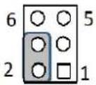 |
| Jumper position for 3.3V (Default) | 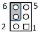 |
| Jumper position for 12V |  |
1.8.3 PWRBTN#/RESET# / HDD LED / Internal Buzzer / External Speaker Header (JFP1)
Table 1.6: JFP1
| Function Jumper Settings | |
| Internal Buzzer (Default) |  |
| 1 7 10 | |
1.8.4 COM1_RI# Pin RI#/5V/12V Selection (JSETCOM1_V1)
Table 1.7: JSETCOM1_V1
| Function Jumper Settings | |
| Jumper position for RI# (Default) |  |
| Jumper position for +5V |  |
Table 1.7: JSETCOM1_V1
| Jumper position for +12V |
1.8.5 COM4_RI# Pin RI#/5V/12V Selection (JSETCOM4_V1)
Table 1.8: JSETCOM4_V1
| Function Jumper Settings | |
| Jumper position for RI# (Default) |  |
| Jumper position for +5V |  |
| Jumper position for +12V |  |
1.8.6 AT/ATX Mode Selection (PSON1)
Table 1.9: PSON1
| Function Jumper Settings | |
| ATX Mode (Default) | 1 2 3 |
| PSON1(2-3) |  |
| AT Mode | 1 2 3 |
| PSON(1-2) | 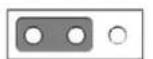 |
1.8.7 Case Open State (NC/NO) Setting Pin Header (JCASEOP_SW1)
Table 1.10: JCASEOP_SW1
| Function Jumper Settings | |
| N.C. (Normal Close) [Default]JCASEOP_SW1(2-3) |  |
1.8.8 MOS Clear Jumper (JCMOS1)
Table 1.11: JCMOS1
Function Jumper Setting
| Normal (Default)JCOMS1(1-2) | 1 2 3 |
| Clear CMOSJCOMS(2-3) | 1 2 3 |
1.8.9 COM3 CCTALK Voltage Selection Header (JCCT_VCON1)
The AIMB-2210 has two sockets for 262-pin DDR5 SODIMMs. These sockets use a 1.2V unbuffered double data rate synchronous DRAM (DDR SDRAM). DRAM is available in capacities of 8GB, 16GB, 32GB and 48GB. The sockets can take any combination with SODIMMs of any size, giving a total memory size between 8GB, 16GB, 64GB and up to max of 96GB. The AIMB-2210 supports error checking and correction (ECC).
1.10 Memory Installation Procedures
To install SODIMMs, first make sure the two handles of the SODIMM socket are in the “open” position, i.e., the handles lean outward. Slowly slide the SODIMM module along the plastic guides on both ends of the socket. Then firmly but gently (avoid pushing down too hard) press the SODIMM module well down into the socket, until you hear a click when the two handles have automatically locked the memory module into the correct position of the SODIMM socket. To remove the memory module, just push both handles outward, and the memory module will be ejected by the mechanism.
Chapter 2
Connecting Peripherals
2.1 Introduction
You can access most of the connectors from the top of the board as it is being installed in the chassis. If you have a number of cards installed or have a packed chassis, you may need to partially remove the card to make all the connections.
2.2 I/O Connector
2.2.1 Dual DisplayPort (DP12)

Table 2.1: Dual DisplayPort (DP12)
| Pin Signal Pin Signal | |
| P1 DP3_0+ P21 DP2_0+ | |
| P2 GND P22 GND | |
| P3 DP3_0- P23 DP2_0- | |
| P4 DP3_1+ P24 DP2_1+ | |
| P5 GND P25 GND | |
| P6 DP3_1- P26 DP2_1- | |
| P7 DP3_2+ P27 DP2_2+ | |
| P8 GND P28 GND | |
| P9 DP3_2- P29 DP2_2- | |
| P10 DP3_3+ P30 DP2_3+ | |
| P11 GND P31 GND | |
| P12 DP3_3- P32 DP2_3- | |
| P13 DP3_HDMI_DNG_DET | P33 DP2_HDMI_DNG_DET |
| P14 GND P34 GND | |
| P15 DP3_AUX+ | P35 DP2_AUX+ |
| P16 GND P36 GND | |
| P17 DP3_AUX- | P37 DP2_AUX- |
| P18 DP3_HPD | P38 DP2_HPD |
| P19 GND P39 GND | |
| P20 +3.3V_DP3 | P40 +3.3V_DP |
2.2.2 Dual DisplayPort (DP34)
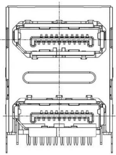
Table 2.2: Dual DisplayPort (DP34)
| Pin Signal Pin Signal | |
| P1 DP3_0+ P21 DP2_0+ | |
| P2 GND P22 GND | |
| P3 DP3_0- P23 DP2_0- | |
| P4 DP3_1+ P24 DP2_1+ | |
| P5 GND P25 GND | |
| P6 DP3_1- P26 DP2_1- | |
| P7 DP3_2+ P27 DP2_2+ | |
| P8 GND P28 GND | |
| P9 DP3_2- P29 DP2_2- | |
| P10 DP3_3+ P30 DP2_3+ | |
| P11 GND P31 GND | |
| P12 DP3_3- P32 DP2_3- | |
| P13 DP3_HDMI_DNG_DET P33 DP2_HDMI_DNG_DET | |
| P14 GND P34 GND | |
| P15 DP3_AUX+ P35 DP2_AUX+ | |
| P16 GND P36 GND | |
| P17 DP3_AUX- | P37 DP2_AUX- |
| P18 DP3_HPD | P38 DP2_HPD |
| P19 GND P39 GND | |
| P20 +3.3V_DP3 | P40 +3.3V_DP |
2.2.3 USB 3.1 Stack Connector * 2 Ports (USB3_12)
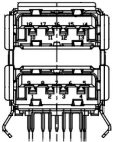
Table 2.3: USB 3.1 Stack Connector * 2 Ports (USB3_12)
Pin Signal Pin Definition Pin Signal Pin Definition
| 1 +5V 10 +5V | |
| 2 USB2_D0- 11 USB2_D1- | |
| 3 USB2_D0+ 12 USB2_D1+ | |
| 4 GND 13 GND | |
| 5 USB31_P0_z_RX- | 14 USB31_P1_z_RX- |
| 6 USB31_P0_z_RX+ | 15 USB31_P1_z_RX+ |
| 7 GND 16 GND | |
| 8 USB31_P0_z_TX- | 17 USB31_P1_z_TX- |
| 9 USB31_P0_z_TX+ | 18 USB31_P1_z_TX+ |
2.2.4 USB 3.1 Stack Connector * 2 Ports (USB_34)
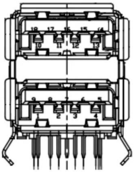
Table 2.4: USB 3.1 Stack Connector * 2 Ports (USB_34)
| Pin Signal Pin Definition Pin Signal Pin Definition | |
| 1 +5V 10 +5V | |
| 2 USB2_D0- 11 USB2_D1- | |
| 3 USB2_D0+ 12 USB2_D1+ | |
| 4 GND 13 GND | |
| 5 USB31_P0_z_RX- 14 USB31_P1_z_RX- | |
| 6 USB31_P0_z_RX+ | 15 USB31_P1_z_RX+ |
| 7 GND 16 GND | |
| 8 USB31_P0_z_TX- | 17 USB31_P1_z_TX- |
| 9 USB31_P0_z_TX+ | 18 USB31_P1_z_TX+ |
2.2.5 RJ-45 Single LAN Port (LAN1)
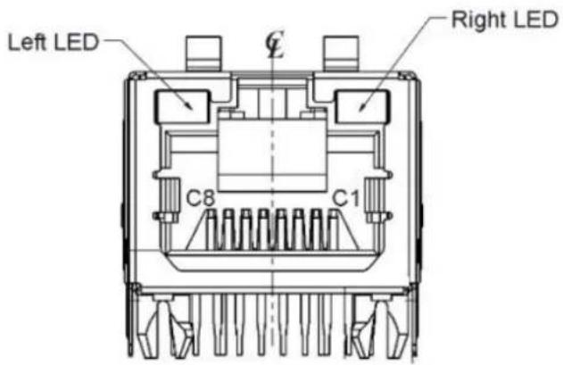
Table 2.5: RJ-45 Single LAN Port (LAN1)
| Pin Signal |
| L1 LAN1_LED1_ACT#_R |
| L2 +V3.3_DUAL |
| L3 LAN1_LED2_1G#_R |
| L4 LAN1_LED0_100M#_R |
| R1 LAN1_MDI0+ |
| R2 LAN1_MDI0- |
| R3 LAN1_MDI1+ |
| R4 LAN1_MDI1- |
| R5 LAN1_CONN |
| R6 LAN1_CT |
| R7 LAN1_MDI2+ |
| R8 LAN1_MDI2- |
| R0 LAN1_MDI3+ |
| R10 LAN1_MDI3- |
| H1 NC |
| H2 NC |
| H3 GND |
| H4 GND |
2.2.6 RJ-45 Single LAN Port (LAN2)

Table 2.6: RJ-45 Single LAN Port (LAN2)
| Pin Signal |
| L1 LAN1_LED1_ACT#_R |
| L2 +V3.3_DUAL |
| L3 LAN1_LED2_1G#_R |
| L4 LAN1_LED0_100M#_R |
| R1 LAN1_MDI0+ |
| R2 LAN1_MDI0- |
| R3 LAN1_MDI1+ |
| R4 LAN1_MDI1- |
| R5 LAN1_CONN |
| R6 LAN1_CT |
| R7 LAN1_MDI2+ |
| R8 LAN1_MDI2- |
| R0 LAN1_MDI3+ |
| R10 LAN1_MDI3- |
| H1 NC |
| H2 NC |
| H3 GND |
| H4 GND |
2.2.7 M.2 E-Key Connector (M2_E1)

Table 2.7: M.2 E-Key Connector (M2_E1)
| Pin Signal Pin Signal | ||
| 1 GND 2 +3.3V | ||
| 3 USB_D+ 4 +3.3V | ||
| 5 USB_D- 6 WLAN_LED1# | ||
| 7 GND 8 BT_PCMCLK | ||
| 9 NC 10 BT_PCMFRM | ||
| 11 NC 12 BT_PCMIN | ||
| 13 | GND 14 BT_PCMOUT | |
| 15 | NC 16 BT_LED# | |
| 17 | NC 18 GND | |
| 19 | GND 20 UART_WAKE# | |
| 21 | NC 22 UART_TXD | |
| 23 | NC 24 Connector Key | |
| 25 | Connector Key | 26 Connector Key |
| 27 | Connector Key | 28 Connector Key |
| 29 | Connector Key | 30 Connector Key |
| 31 | Connector Key | 32 UART_RXD |
| 33 | GND 34 UART_RTS | |
| Pin | Signal | Pin Signal |
| 35 | PETp0 | 36 UART_CTS |
| 37 | PETn0 | 38 NC |
| 39 | GND 40 NC | |
| 41 | PERp0 | 42 NC |
| 43 | PERn0 | 44 NC |
| 45 | GND 46 NC | |
| 47 | REFCLKp0 | 48 NC |
| 49 | REFCLKn0 | 50 SUSCLK |
| 51 | GND 52 WLAN_RST# | |
| 53 | CLKREQ0# | 54 BT_RF_KILL# |
| 55 | PEWAKE0# | 56 WIFI_RF_KILL# |
| 57 | GND 58 NC | |
| 59 | NC 60 NC | |
| 61 | NC 62 NC | |
| 63 | GND 64 NC | |
| 65 | NC 66 NC | |
Table 2.7: M.2 E-Key Connector (M2_E1)
| 67 NC 68 NC |
| 69 GND 70 NC |
| 71 NC 72 +3.3V |
| 73 NC 74 +3.3V |
| 75 GND |
2.2.8 M.2 M-Key Connector (M2_M1)

Table 2.8: M.2 M-Key Connector (M2_M1)
| Pin Signal Pin Signal | |
| 1 GND 2 3.3V | |
| 3 GND 4 3.3V | |
| 5 PERn3 6 N/C | |
| 7 PERp3 8 N/C | |
| 9 GND 10 DAS/DSS# (I/O)/LED1# (I)(0/3.3V) | |
| 11 PETn3 | 12 3.3V |
| 13 PETp3 | 14 3.3V |
| 15 GND 16 3.3V | |
| 17 PERn2 18 3.3V | |
| 19 PERp2 20 N/C | |
| 21 GND 22 N/C | |
| 23 PETn2 | 24 N/C |
| 25 PETp2 | 26 N/C |
| 27 GND 28 N/C | |
| 29 PERn1 30 N/C | |
| 31 PERp1 32 N/C | |
| Pin Signal | Pin Signal |
| 33 GND 34 N/C | |
| 35 PETn1 | 36 N/C |
| 37 PETp1 | 38 DEVSLP (O) |
| 39 GND 40 N/C | |
| 41 PERn0/SATA-B+ | 42 N/C |
| 43 PERp0/SATA-B- | 44 N/C |
| 45 GND 46 N/C | |
| 47 PETn0/SATA-A- | 48 N/C |
| 49 PETp0/SATA-A+ | 50 PERST# (O)(0/3.3V) or N/C |
| 51 GND 52 CLKREQ# (I/O)(0/3.3V) or N/C | |
Table 2.8: M.2 M-Key Connector (M2_M1)
| 53 REFCLKn 54 PEWAKE# (I/O)(0/3.3V) or N/C |
| 55 REFCLKp 56 N/C |
| 57 GND 58 N/C |
| 59 Connector Key 60 Connector Key |
| 61 Connector Key 62 Connector Key |
| 63 Connector Key 64 Connector Key |
| 65 Connector Key 66 Connector Key |
| 67 N/C 68 SUSCLK(32kHz) (O)(0/3.3V) |
| 69 PEDET (NC-PCIe/GND-SATA) 70 3.3V |
| 71 GND 72 3.3V |
| 73 GND 74 3.3V |
| 75 GND |
2.2.9 M.2 M-Key Connector (M2_M2)

Table 2.9: M.2 M-Key Connector (M2_M2)
| Pin Signal Pin Signal | ||||
| 1 | GND 2 | 3.3V | ||
| 3 | GND 4 | 3.3V | ||
| 5 | PERn3 | 6 | N/C | |
| 7 | PERp3 | 8 | N/C | |
| 9 | GND 10 | DAS/DSS# (I/O)/LED1# (I)(0/3.3V) | ||
| 11 | PETn3 | 12 | 3.3V | |
| 13 | PETp3 | 14 | 3.3V | |
| 15 | GND 16 | 3.3V | ||
| 17 | PERn2 | 18 | 3.3V | |
| 19 | PERp2 | 20 | N/C | |
| 21 | GND 22 | N/C | ||
| 23 | PETn2 | 24 | N/C | |
| 25 | PETp2 | 26 | N/C | |
| 27 | GND 28 | N/C | ||
| 29 | PERn1 | 30 | N/C | |
| 31 | PERp1 | 32 | N/C | |
| Pin | Signal | Pin | Signal | |
| 33 | GND 34 | N/C | ||
| 35 | PETn1 | 36 | N/C | |
| 37 | PETp1 | 38 | DEVSLP (O) | |
Table 2.9: M.2 M-Key Connector (M2_M2)
| 39 GND 40 N/C |
| 41 PERn0/SATA-B+ 42 N/C |
| 43 PERp0/SATA-B- 44 N/C |
| 45 GND 46 N/C |
| 47 PETn0/SATA-A- 48 N/C |
| 49 PETp0/SATA-A+ 50 PERST# (O)(0/3.3V) or N/C |
| 51 GND 52 CLKREQ# (I/O)(0/3.3V) or N/C |
| 53 REFCLKn 54 PEWAKE# (I/O)(0/3.3V) or N/C |
| 55 REFCLKp 56 N/C |
| 57 GND 58 N/C |
| 59 Connector Key 60 Connector Key |
| 61 Connector Key 62 Connector Key |
| 63 Connector Key 64 Connector Key |
| 65 Connector Key 66 Connector Key |
| 67 N/C 68 SUSCLK(32kHz) (O)(0/3.3V) |
| 69 PEDET (NC-PCIe/GND-SATA) 70 3.3V |
| 71 GND 72 3.3V |
| 73 GND 74 3.3V |
| 75 GND |
2.2.10 12V Power Supply Connector (DCIN1)
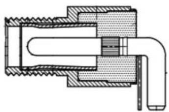

BOTTOM VIEW

REAR VIEW
Table 2.10: 12V Power Supply Connector (DCIN1)
| Pin | Signal |
| 1 | +12V ~ +24V |
| 2 | GND |
| 3 | GND |
2.2.11 SATA Connector (SATA1)
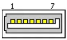
Table 2.11: SATA Connector (SATA1)
| Pin Signal |
| 1 GND |
| 2 TX+ |
| 3 TX- |
| 4 GND |
| 5 RX- |
| 6 RX+ |
| 7 GND |
2.2.12 SATA Connector (SATA2)
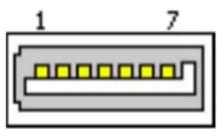
Table 2.12: SATA Connector (SATA2)
| Pin Signal |
| 1 GND |
| 2 TX+ |
| 3 TX- |
| 4 GND |
| 5 RX- |
| 6 RX+ |
| 7 GND |
2.2.13 PCIe x16 Connector (PCIEX16_1)

Table 2.13: PCIe x16 Connector (PCIEX16_1)
| Pin Signal Pin Definition Pin Signal Pin Definition | ||||
| B1 12V_1 A1 PRSNT1 | ||||
| B2 12V_2 A2 12V_4 | ||||
| B3 12V_3 A3 12V_5 | ||||
| B4 GND_1 A4 GND_3 | ||||
| B5 SMCLK A5 JTAG2 | ||||
| B6 SMDAT A6 JTAG3 | ||||
| B7 GND_2 A7 JTAG4 | ||||
| B8 3_3V_1 A8 JTAG5 | ||||
| B9 JTAG1 A9 3_3V_2 | ||||
| B10 3_3VAUX | A10 3_3V_3 | |||
| B11 WAKE | A11 PWRGD | |||
| B12 | RSVD_1 | A12 GND_7 | ||
| B13 | GND_4 A13 | REFCLK+ | ||
| B14 | HSOP0 A14 | REFCLK | ||
| B15 | HSON0 A15 | GND_8 | ||
| B16 | GND_5 A16 | HSIP0 | ||
| B17 | PRSNT2_1 | A17 HSIN0 | ||
| B18 | GND_6 A18 | GND_9 | ||
| B19 | HSOP1 A19 | RSVD_3 | ||
| B20 | HSON1 A20 | GND_16 | ||
| B21 | GND_10 | A21 HSIP1 | ||
| B22 | GND_11 | A22 HSIN1 | ||
| B23 | HSOP2 A23 | GND_17 | ||
| B24 | HSON2 A24 | GND_18 | ||
| B25 | GND_12 | A25 HSIP2 | ||
| B26 | GND_13 | A26 HSIN2 | ||
| B27 | HSOP3 A27 | GND_19 | ||
| B28 | HSON3 A28 | GND_20 | ||
| B29 | GND_14 | A29 HSIP3 | ||
| B30 | RSVD_2 | A30 HSIN3 | ||
| B31 | PRSNT2_2 | A31 GND_21 | ||
| B32 | GND_15 | A32 RSVD_4 | ||
| B33 | HSOP4 A33 | RSVD_5 | ||
| B34 | HSON4 A34 | GND_30 | ||
| B35 | GND_22 | A35 HSIP4 | ||
Table 2.13: PCIe x16 Connector (PCIEX16_1)
| B36 GND_23 A36 HSIN4 |
| B37 HSOP5 A37 GND_31 |
| B38 HSON5 A38 GND_32 |
| B39 GND_24 A39 HSIP5 |
| B40 GND_25 A40 HSIN5 |
| B41 HSOP6 A41 GND_33 |
| B42 HSON6 A42 GND_34 |
| B43 GND_26 A43 HSIP6 |
| B44 GND_27 A44 HSIN6 |
| B44 GND_27 A45 GND_35 |
| B46 HSON7 A46 GND_36 |
| B47 GND_28 A47 HSIP7 |
| B48 PRSNT2_3 A48 HSIN7 |
| B49 GND_29 A49 GND_37 |
| B50 HSOP8 A50 RSVD_7 |
| B51 HSON8 A51 GND_53 |
| B52 GND_38 A52 HSIP8 |
| B53 GND_39 A53 HSIN8 |
| B54 HSOP9 A54 GND_54 |
| B55 HSON9 A55 GND_55 |
| B56 GND_40 A56 HSIP9 |
| B57 GND_41 A57 HSIN9 |
| B58 HSOP10 A58 GND_56 |
| B59 HSON10 A59 GND_57 |
| B60 GND_42 A60 HSIP10 |
| B61 GND_43 A61 HSIN10 |
| B62 HSOP11 A62 GND_58 |
| B63 HSON11 A63 GND_59 |
| B64 GND_44 A64 HSIP11 |
| B65 GND_45 A65 HSIN11 |
| B66 HSOP12 A66 GND_60 |
| B67 HSON12 A67 GND_61 |
| B68 GND_46 A68 HSIP12 |
| B69 GND_47 A69 HSIN12 |
| B70 HSOP13 A70 GND_62 |
| B71 HSON13 A71 GND_63 |
| B72 GND_48 A72 HSIP13 |
| B73 GND_49 A73 HSIN13 |
| B74 HSOP14 A74 GND_64 |
| B75 HSON14 A75 GND_65 |
| B76 GND_50 A76 HSIP14 |
| B77 GND_51 A77 HSIN14 |
| B78 HSOP15 A78 GND_66 |
| B79 HSON15 A79 GND_67 |
| B80 GND_52 A80 HSIP15 |
| B81 PRSNT2_4 A81 HSIN15 |
| B82 RSVD_6 A82 GND_68 |
2.2.14 HD Analog Audio Interface Line-Out (AUDIO1)

Table 2.14: HD Analog Audio Interface Line-Out (AUDIO1)
| Pin Signal Pin Definition |
| 1 GND_A |
| 2 A_Z_LINEO-L |
| 3 GND_A |
| 4 A_Z_LINEO-R |
| 5 A_FRONT-JD |
2.2.15 HD Analog Audio Interface Mic-In (AUDIO2)

Table 2.15: HD Analog Audio Interface Mic-In (AUDIO2)
| Pin Signal Pin Definition |
| 1 GND_A |
| 2 A_Z_MIC1-L |
| 3 GND_A |
| 4 A_Z_MIC1-R |
| 5 A_MIC1-JD |
2.2.16 DDR5 SODIMM Socket A1 (DIMMA1)
Please refer to the JEDEC standard.
2.2.17 DDR5 SODIMM Socket B1 (DIMMB1)
Please refer to the JEDEC standard.
2.3 Box Header
2.3.1 EDP Connector / LVDS Connector (EDP1_LVDS1)

Table 2.16: LVDS1
| Pin Signal Pin Signal | ||
| 1 VDD 2 VDD | ||
| 3 LVDS DETECT# 4 GND | ||
| 5 VDD 6 VDD | ||
| 7 LVDS_OD0- 8 LVDS_ED0- | ||
| 9 LVDS_OD0+ 10 LVDS_ED0+ | ||
| 11 | GND | 12 GND |
| 13 | LVDS_OD1- 14 LVDS_ED1- | |
| 15 | LVDS_OD1+ 16 LVDS_ED1+ | |
| 17 | GND | 18 GND |
| 19 | LVDS_OD2- 20 LVDS_ED2- | |
| 21 | LVDS_OD2+ 22 LVDS_ED2+ | |
| 23 | GND | 24 GND |
| 25 | LVDS_OCK- | 26 LVDS_ECK- |
| 27 | LVDS_OCK+ | 28 LVDS_ECK+ |
| 29 | GND | 30 GND |
| 31 | N.C | 32 N.C |
| 33 | GND | 34 GND |
| 35 | LVDS_OD3- 36 LVDS_ED3- | |
| 37 | LVDS_OD3+ 38 LVDS_ED3+ | |
| 39 | N.C | 40 LVDS VCON |
| Table 2.17: EDP1 | ||
| Pin Signal Pin Signal | ||
| 1 VDD 2 VDD | ||
| 3 LVDS DETECT# 4 GND | ||
| 5 VDD 6 VDD | ||
| 7 EDP_TX2- 8 N.C | ||
| 9 EDP_TX2+ 10 N.C | ||
| 11 | GND | 12 GND |
| 13 | EDP_TX1- 14 N.C | |
| 15 | EDP_TX1+ 16 N.C | |
| 17 | GND | 18 GND |
| 19 | EDP_TX0- 20 N.C | |
| 21 | EDP_TX0+ 22 N.C | |
| 23 | GND | 24 GND |
| 25 | EDP_TX3- 26 N.C | |
| 27 | EDP_TX3+ 28 N.C | |
| 29 | GND | 30 GND |
| 31 | EDP_AUX+ | 32 EDP_AUX- |
| 33 | GND | 34 EDP_HPD |
| 35 | N.C | 36 N.C |
| 37 | N.C | 38 N.C |
| 39 | N.C | 40 GND |
2.3.2 Internal USB 2.0 Connector * 2 Ports (USB56)

Table 2.18: Internal USB 2.0 Connector * 2 Ports (USB56)
| Pin Signal Pin | Signal | ||
| 1 N.C | 2 | GND | |
| 3 GND | 4 | GND | |
| 5 D+ | 6 | D+ | |
| 7 D- | 8 | D- | |
| 9 VBUS | 10 | VBUS |
2.3.3 Internal USB 2.0 Connector * 2 Ports (USB78)

Table 2.19: Internal USB 2.0 Connector * 2 Ports (USB78)
| Pin Signal Pin Signal |
| 1 N.C 2 GND |
| 3 GND 4 GND |
| 5 D+ 6 D+ |
| 7 D- 8 D- |
| 9 VBUS 10 VBUS |
2.3.4 COM1 Connector (COM1)
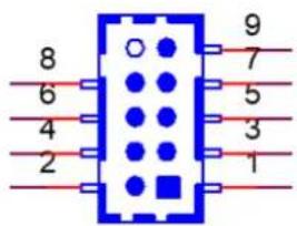
Table 2.20: COM1 Connector (COM1)
| Pin Signal Pin Signal | |
| 1 DCD# 2 SIN | |
| 3 SOUT | 4 DTR |
| 5 GND 6 DSR# | |
| 7 RTS# | 8 CTS# |
| 9 RI | |
2.3.5 COM2 Connector (COM2)

Table 2.21: COM2 Connector (COM2)
| Pin Signal Pin Signal | |
| 1 DCD# 2 SIN | |
| 3 SOUT 4 DTR | |
| 5 GND 6 DSR# | |
| 7 RTS# 8 CTS# | |
| 9 RI |
2.3.6 COM3 Connector (COM3)

Table 2.22: COM3 Connector (COM3)
| Pin Signal Pin Signal | |||
| 1 DCD# 2 | SIN | ||
| 3 SOUT | 4 | DTR | |
| 5 GND | 6 | DSR# | |
| 7 RTS# | 8 | CTS# | |
| 9 | RI | ||
2.3.7 COM4 Connector (COM4)

Table 2.23: COM4 Connector (COM4)
| Pin Signal Pin Signal | |
| 1 DCD# 2 SIN | |
| 3 SOUT 4 DTR | |
| 5 GND 6 DSR# | |
| 7 RTS# 8 CTS# | |
| 9 RI |
2.3.8 COM4 Connector (COM5)

Table 2.24: COM4 Connector (COM5)
| Pin Signal Pin Signal | |
| 1 DCD# 2 SIN | |
| 3 SOUT 4 DTR | |
| 5 GND 6 DSR# | |
| 7 RTS# 8 CTS# | |
| 9 RI |
2.3.9 COM4 Connector (COM6)

Table 2.25: COM4 Connector (COM6)
| Pin Signal Pin Signal | |
| 1 DCD# 2 SIN | |
| 3 SOUT 4 DTR | |
| 5 GND 6 DSR# | |
| 7 RTS# 8 CTS# | |
| 9 RI |
2.3.10 CMOS Battery Connector (BAT1)
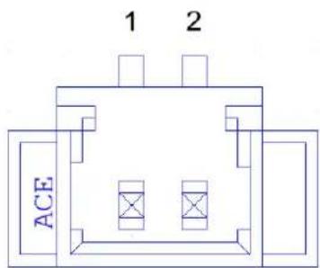
Table 2.26: CMOS Battery Connector (BAT1)
| Pin Signal | |
| 1 | +VBAT |
| 2 | GND |
2.3.11 EDP/LVDS Backlight Inverter Power Connector (INV1)

Table 2.27: EDP/LVDS Backlight Inverter Power Connector (INV1)
Table 2.28: ATX 4-Pin Power Connector (ATX12V1)
| Pin Signal Pin Signal |
| 1 GND 2 GND |
| 3 +12V 4 +12V |
2.3.13 ATX 5V/PSON Connector (ATX_5VSB1)
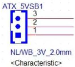
Table 2.29: ATX 5V/PSON Connector (ATX_5VSB1)
| Pin Signal |
| 1 ATX_5V |
| 2 GND |
| 3 PS_ON# |
2.3.14 SATA Power Connector (SATA_PWR1)

Table 2.30: SATA Power Connector (SATA_PWR1)
| Pin Signal |
| 1 +V5 |
| 2 GND |
| 3 GND |
| 4 +V12 |
2.3.15 SATA Power Connector (SATA_PWR2)
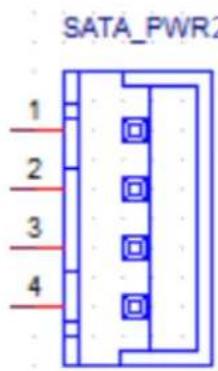
Table 2.31: SATA Power Connector (SATA_PWR2)
| Pin Signal |
| 1 +V5 |
| 2 GND |
| 3 GND |
| 4 +V12 |
2.4 Pin Header
2.4.1 Power LED Pin Header (JFP2)
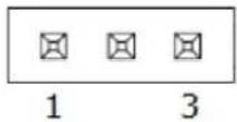
Table 2.32: Power LED Pin Header (JFP2)
| Pin Signal | |
| 1 Power LED+ | |
| 2 | NC |
| 3 Power LED- | |
2.4.2 SPI BIOS Flash Socket1 (SPI1)
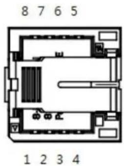
Table 2.33: SPI BIOS Flash Socket1 (SPI1)
| Pin Signal Pin Signal |
| 1 CS# 5 MOSI |
| 2 MISO 6 SCLK |
| 3 WP# / IO2 7 HOLD# / IO3 |
| 4 GND 8 +V1.8_SPI |
2.4.3 SPI BIOS Debug Header (SPI_CN1)
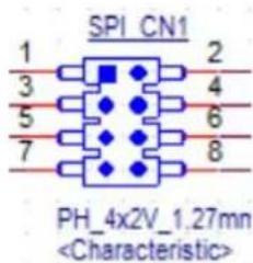
Table 2.34: SPI BIOS Debug Header (SPI_CN1)
| Pin Signal Pin Signal | ||
| 1 CS# | 5 | WP |
| 2 +V1.8_SPI | 6 | CLK |
| 3 MISO | 7 | GND |
| 4 HOLD | 8 | MOSI |
2.4.4 8-Bit General Purpose I/O Pin Header (GPIO1)
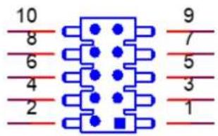
Table 2.35: 8-Bit General Purpose I/O Pin Header (GPIO1)
| Pin Signal Pin Signal |
| 1 GPIO0 2 GPIO4 |
| 3 GPIO1 4 GPIO5 |
| 5 GPIO2 6 GPIO6 |
| 7 GPIO3 8 GPIO7 |
| 9 VCC_GPIO 10 GND |
2.4.5 8-Bit General Purpose I/O Pin Header (GPIO2)

Table 2.36: 8-Bit General Purpose I/O Pin Header (GPIO2)
| Pin Signal Pin Signal |
| 1 GPIO8 2 GPIO12 |
| 3 GPIO9 4 GPIO13 |
| 5 GPIO10 6 GPIO14 |
| 7 GPIO11 8 GPIO15 |
| 9 VCC_GPIO 10 GND |
2.4.6 CPU FAN Connector (CPUFAN1)
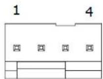
Table 2.37: CPU FAN Connector (CPUFAN1)
| Pin | Signal |
| 1 | GND |
| 2 | CPU FAN VCC |
| 3 | CPU FAN SPEED |
| 4 | CPU FAN PWM |
2.4.7 System Fan Connector (SYSFAN1)

Table 2.38: System Fan Connector (SYSFAN1)
| Pin Signal |
| 1 GND |
| 2 CPU FAN VCC |
| 3 CPU FAN SPEED |
| 4 CPU FAN PWM |
2.4.8 Case Open Connector (JCASE1)
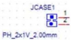
Table 2.39: Case Open Connector (JCASE1)
| Pin Signal |
| 1 CASEOP |
| 2 GND |
2.4.9 VCORE Programming Header (VR_PMB1)

Table 2.40: VCORE Programming Header (VR_PMB1)
| Pin Signal |
| 1 VR_SDATA |
| 2 GND |
| 3 VR_SCLK |
2.4.10 HD Digital Audio Interface S/PDIF Out (SPDIF1)

Table 2.41: HD Digital Audio Interface S/PDIF Out (SPDIF1)
| Pin Signal Pin Definition | |
| 1 +5V | |
| 2 | NA |
| 3 SPDIF OUT | |
| 4 GND | |
2.4.11 Audio Amplifier Output Pin Header (AMP1)
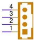
AMP1
Table 2.42: Audio Amplifier Output Pin Header (AMP1)
| Pin Signal |
| 1 AMP OUT - R+ |
| 2 AMP OUT - R- |
| 3 AMP OUT - L- |
| 4 AMP OUT - L+ |
2.4.12 HD Analog Audio Interface Front Panel (FPAUD1)

2.5.5 PWRBTN# / RESET# / HDD LED / Serial Bus from HW Monitor IC / Internal Buzzer / External Speaker Header (JFP1)

Table 2.49: PWRBTN# / RESET#/HDD LED / Serial Bus from HW Monitor IC / Internal Buzzer / External Speaker Header (JFP1)
| Pin Signal Pin Signal | |||
| 1 +5V 2 HDD LED+ | |||
| 3 Power Button+ 4 SPK_P2 | |||
| 5 HDD LED- | 6 Power Button- | ||
| 7 SPK_P3 | 8 SMB_DATA | ||
| 9 System Reset+ | 10 | SPK_P4 | |
| 11 SMB_CLK | 12 | System Reset- | |
2.5.6 Case Open Signal Reverse Header (JCASEOP_SW1)

Table 2.50: Case Open Signal Reverse Header (JCASEOP_SW1)
| Pin Signal |
| 1 CASEOP# |
| 2 HWM_CASEOP# |
| 3 CASEOP |
2.5.7 CMOS Reset Header (JCMOS1)

PH 3x1V 2.00mm
PH3x1P-2.00
Table 2.51: CMOS Reset Header (JCMOS1)
| Pin Signal | |
| 1 | NC |
| 2 RTCRST# | |
| 3 RTCRST#_PD | |
2.5.8 AT/ATX Mode Selection (PSON1)

PSON1
PH 3x1V 2.00mm
PH3x1P-2.00
Table 2.52: AT/ATX Mode Selection (PSON1)
| Pin Signal |
| 1 VCCAT |
| 2 +V3_Pull High |
| 3 VCCATX |
With the AMI BIOS Setup program, you can modify BIOS settings and control the special features of your computer. The Setup program uses a number of menus for making changes and turning special features on or off. This chapter describes the basic navigation of the AIMB-2210 setup screens.
3.2 BIOS Setup
The AIMB-2210 Series system has AMI BIOS built in, with a CMOS SETUP utility that allows users to configure required settings or to activate certain system features. The CMOS SETUP saves the configuration in the CMOS RAM of the motherboard. When the power is turned off, the battery on the board supplies the necessary power to preserve the CMOS RAM.
When the power is turned on, press the button during the BIOS POST (Power-On Self-Test) to access the CMOS SETUP screen.
Table 3.1: Control Keys
| <↑><↓><←><→>Move to select item | |
| Select item | |
| Main Menu - Quit and do not save changes into CMOSSub-Menu - Exit the current page and return to the Main Menu | |
| Increase the numeric value or make changes | |
| Decrease the numeric value or make changes | |
| General help, for the Setup Sub-Menu | |
| Item Help | |
| Load Previous Values | |
| Load Setup Defaults | |
| Save all CMOS changes | |
3.2.1 Main Menu
Press to enter the AMI BIOS CMOS Setup Utility. The Main Menu will appear on the screen. Use the arrow keys to select among the items and press
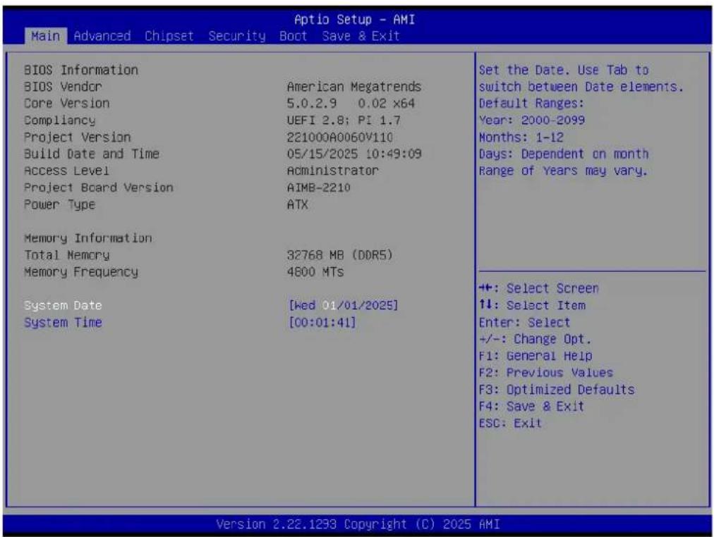
The Main BIOS setup screen has two main frames. The left frame displays all the options that can be configured. Grayed-out options cannot be configured; options in blue can. The right frame displays the legend. Above the legend is an area reserved for a text message. When an option is selected in the left frame, it is highlighted in white. Often a text message will accompany it.
■ System Time / System Data
Use this option to change the system time and date. Highlight the System Time or System Date using the keys. Enter new values via the keyboard. Press the
3.2.2 Advanced BIOS Features
Select the Advanced tab from the AIMB-2210 setup menu to enter the Advanced BIOS setup page. Users can select any item in the left frame of the screen, such as CPU configuration. Select an Advanced BIOS setup option by highlighting the text using the keys. All Advanced BIOS setup options are described in this section. The Advanced BIOS setup menu screen is shown below. The sub-menus are described on the following pages.
| Aptio Setup - AMI Main Advanced Chipset Security Boot Save & Exit | |
| Trusted Computing ACPI Settings AMD CBS AMD PBS NCT6126D Super IO Configuration NCT6126D HW Monitor S5 RTC Wake Settings UEFI Variables Protection Serial Port Console Redirection CPU Configuration USB Configuration Network Stack Configuration NVMe Configuration Asmedia AHCI Controller | Trusted Computing Settings |
| +: Select Screen ↑↓: Select Item Enter: Select +/-: Change Opt. F1: General Help F2: Previous Values F3: Optimized Defaults F4: Save & Exit ESC: Exit | |
3.2.2.1 Trust Computing
Advanced → Trust Computing
| TPM 2.0 Device Found Firmware Version: 15.23 Vendor: IFX | Enables or Disables BIOS support for security device. 0.S. will not show Security Device. TCG EFI protocol and INT1A interface will not be available. | |
| Security Device Support [Enable] Active PCR banks SHA256 Available PCR banks SHA256,SHA384 | ||
| SHA256 FCR Bank [Enabled] SHA384 FCR Bank [Disabled] | ||
| Pending operation [None] Platform Hierarchy [Enabled] Storage Hierarchy [Enabled] Endorsement Hierarchy [Enabled] Physical Presence Spec Version [1.3] TPM 2.0 InterfaceType [TIS] PH Randomization [Enabled] Device Select [Auto] | +: Select Screen 11: Select Item Enter: Select +/-: Change Opt. F1: General Help F2: Previous Values F3: Optimized Defaults F4: Save & Exit ESC: Exit | |
3.2.2.2 ACPI settings
Advanced → ACPI settings
![Advanced ACPI Settings Enable ACPI Auto Configuration [Disabled] Enable Hibernation [Enabled] Enables or Disables BIOS ACPI Auto Configuration. ++: Select Screen ↑↓: Select Item Enter: Select +/-: Change Opt. F1: General Help F2: Previous Values F3: Optimized Defaults F4: Save & Exit ESC: Exit Versi…](/content/2026/07/1486455/images/4fca69c443c4c6d8a0566422d0cb2ad1bff5df0b5bcd47467dfa42192df1dd2a.jpg)
3.2.2.3 AMD CBS
Advanced → AMD CBS

CPU Common Options
Advanced → AMD CBS → CPU Common Options
![Advanced CPU Common Options Core Performance Boost [Auto] Global C-state Control [Auto] Disable CPB +: Select Screen 1↓: Select Item Enter: Select +/-: Change Opt. F1: General Help F2: Previous Values F3: Optimized Defaults F4: Save & Exit ESC: Exit Version 2.22.1293 Copyright (C) 2025 AMI](/content/2026/07/1486455/images/fb31b755ddb05dcdc2c52a703a2a4fd151131655d3050c4f04748c9e9550c830.jpg)
UMC Common Options
Advanced → AMD CBS → UMC Common Options

DDR Options
Advanced → AMD CBS → UMC Common Options → DDR Options
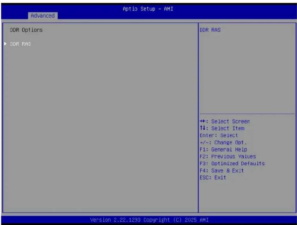
DDR RAS
Advanced → AMD CBS → UMC Common Options → DDR Options → DDR RAS
![Advanced Aptio Setup - AMI DDR RAS Disable Memory Error Injection [Auto] ▶ DDR ECC Configuration True: UMC::CH::MiscCfg[DisErrInj]=1 +: Select Screen ↑↓: Select Item Enter: Select +/-: Change Opt. F1: General Help F2: Previous Values F3: Optimized Defaults F4: Save & Exit ESC: Exit Version 2.22.1233…](/content/2026/07/1486455/images/b788b589885ae12d10127f6ef9a5e794b5b1a5bb79142b760b0b5078d37d612b.jpg)
DDR ECC Configuration
Advanced → AMD CBS → UMC Common Options → DDR Options → DDR RAS → DDR ECC configuration

NBIO Common Options
Advanced → AMD CBS → NBIO Common Options
![Advanced Aptio Setup - AMI NBIO Common Options PSPP Policy [Auto] Audio Configuration No help string ++: Select Screen 1↓: Select Item Enter: Select +/-: Change Opt. F1: General Help F2: Previous Values F3: Optimized Defaults F4: Save & Exit ESC: Exit Version 2.22.1233 Copyright (C) 2025 AMI](/content/2026/07/1486455/images/55ba005125bb2b4f21104b7487ffd7cdb33a6552ad1b939e5c0704f287c16436.jpg)
Audio Configuration
Advanced → AMD CBS → NBIO Common Options → Audio Configuration
![Advanced Audio Configuration NB Azalia [Auto] HD Audio Enable [Enabled] Audio IOs [Auto] Enable Integrate HD Audio controller +: Select Screen ↑↓: Select Item Enter: Select +/-: Change Opt. F1: General Help F2: Previous Values F3: Optimized Defaults F4: Save & Exit ESC: Exit Version 2.22.1233 Copyri…](/content/2026/07/1486455/images/7107e118d89d16fe1c901f736dfdd043682355330a6f40fb5316a6ae7463f888.jpg)
FCH Common Options
Advanced → AMD CBS → FCH Common Options
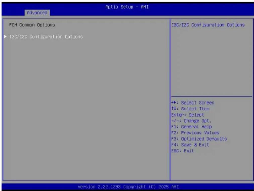
I3C/I2C Configuration Options
Advanced → AMD CBS → FCH Common Options → I3C/I2C Configuration Options
![Advanced I3C/I2C Configuration Options I3C/I2C 2 Enable [Auto] I3C/I2C 3 Enable [Auto] No help string +: Select Screen ↓: Select Item Enter: Select +/-: Change Opt. F1: General Help F2: Previous Values F3: Optimized Defaults F4: Save & Exit ESC: Exit Version 2.22.1238 Copyright (C) 2025 AMI](/content/2026/07/1486455/images/bd7dec38b84c4b9ff5fac70821a2bdcb5cb254dc1242c8e2f85b1eba84452012.jpg)
SOC Miscellaneous Control
Advanced → AMD CBS → SOC Miscellaneous Control
![Advanced Aptio Setup - AMI SOC Miscellaneous Control Trusted Platform Module [Enable dTPM] Enable/Disable TFM physical presence. +: Select Screen 11: Select Item Enter: Select +/-: Change Opt. F1: General Help F2: Previous Values F3: Optimized Defaults F4: Save & Exit ESC: Exit Version 2.22.1233 Cop…](/content/2026/07/1486455/images/fe63f106a2a6c82e4f935859275e818d1eb553ba5d9311a379aaf0b701d5c779.jpg)
3.2.2.4 AMD PBS
Advanced → AMD PBS
![Advanced ▶ AMD Firmware Version ▶ PCI Express Configurations Above 4GB MMID Limit [40bit (1TB)] Show all of AMD Firmware Version +: Select Screen ↑↓: Select Item Enter: Select +/-: Change Opt. F1: General Help F2: Previous Values F3: Optimized Defaults F4: Save & Exit ESC: Exit Version 2.22.1233 Cop…](/content/2026/07/1486455/images/9e185c1b7d1ba1576ec2b7f427e13e41af22f6369fce53d3c7d988c8b73bf109.jpg)
AMD Firmware Version
Advanced → AMD PBS → AMD Firmware Version

PCI Express Configurations
Advanced → AMD PBS → AMD Firmware Version → PCI Express Configurations
![Advanced Aptio Setup - AMI PCI Express Configurations NVMe RAID mode [Disabled] Enable or disable NVMe RAID mode. Please setting the 'PCIe/GFX Lanes Configuration' item according to the RAID configuration +: Select Screen 1↓: Select Item Enter: Select +/-: Change Opt. F1: General Help F2: Previous V…](/content/2026/07/1486455/images/798395f3d23f11ab124a80346eb0264c635bf7013722538d9988f429f3d71bd1.jpg)
3.2.2.5 NCT6126D Super IO Configuration
Advanced → NCT6126D Super IO Configuration
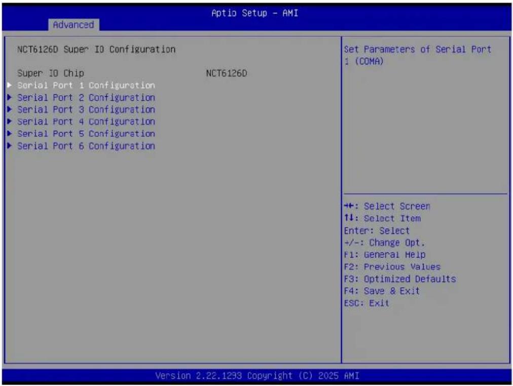
Serial Port 1 Configuration
Advanced → NCT6126D Super IO Configuration → Serial Port 1 Configuration
![Advanced Serial Port 1 Configuration Serial Port [Enabled] Device Settings IC=3F9h; IRQ=4; Enable or Disable Serial Port (COM) +: Select Screen 1↓: Select Item Enter: Select +/-: Change Opt. F1: General Help F2: Previous Values F3: Optimized Defaults F4: Save & Exit ESC: Exit Version 2.22.1238 Copyr…](/content/2026/07/1486455/images/5a8a585a997396acf712a3657f1d40d0b0f4383005e6ce9361ff43af02f981d3.jpg)
Serial Port 2 Configuration
Advanced → NCT6126D Super IO Configuration → Serial Port 2 Configuration
![Advanced Aptio Setup - AMI Serial Port 2 Configuration Serial Port [Enabled] Device Settings IC=2F3h; IRQ=3; Enable or Disable Serial Port (COM) +: Select Screen ↑↓: Select Item Enter: Select +/-: Change Opt. F1: General Help F2: Previous Values F3: Optimized Defaults F4: Save & Exit ESC: Exit Versi…](/content/2026/07/1486455/images/e0ccbdfa4f3fdb607843d45ef522378049653aef7f0d10f5fd3ca0529c18fd60.jpg)
Serial Port 3 Configuration
Advanced → NCT6126D Super IO Configuration → Serial Port 3 Configuration
![Advanced Serial Port 3 Configuration Serial Port [Enabled] Device Settings IC=3E3h; IRQ=5; Enable or Disable Serial Port (COM) +: Select Screen 1↓: Select Item Enter: Select +/-: Change Opt. F1: General Help F2: Previous Values F3: Optimized Defaults F4: Save & Exit ESC: Exit Version 2.22.1233 Copyr…](/content/2026/07/1486455/images/b00a99d3612489c24e617d0ed12814af2d357e2dc87c4792a05d0ba4df350a47.jpg)
Serial Port 4 Configuration
Advanced → NCT6126D Super IO Configuration → Serial Port 4 Configuration
![Advanced Optio Setup - AMI Serial Port 4 Configuration Serial Port [Enabled] Device Settings IO=2E3h; IRQ=6; Enable or Disable Serial Port (COM) +: Select Screen 11: Select Item Enter: Select +/-: Change Opt. F1: General Help F2: Previous Values F3: Optimized Defaults F4: Save & Exit ESC: Exit Versi…](/content/2026/07/1486455/images/81090910a595b4a623a7d00b88ac5f5f385d040c18feadb462642492402d56a8.jpg)
Serial Port 5 Configuration
Advanced → NCT6126D Super IO Configuration → Serial Port 5 Configuration
![Advanced Aptio Setup - AMI Serial Port 5 Configuration Serial Port [Enabled] Device Settings IC=220h; IRQ=10; Enable or Disable Serial Port (COM) +: Select Screen 1↓: Select Item Enter: Select +/-: Change Opt. F1: General Help F2: Previous Values F3: Optimized Defaults F4: Save & Exit ESC: Exit Vers…](/content/2026/07/1486455/images/dd3a2b33fba7ba7856cfb589eab86d3a1dc3ee1670321bd9edaa77e15169a8b9.jpg)
Serial Port 6 Configuration
Advanced → NCT6126D Super IO Configuration → Serial Port 6 Configuration
![Advanced Aptio Setup - AMI Serial Port 6 Configuration Serial Port [Enabled] Device Settings IC=223h; IRQ=11; Enable or Disable Serial Port (COM) +: Select Screen ↑↓: Select Item Enter: Select +/-: Change Opt. F1: General Help F2: Previous Values F3: Optimized Defaults F4: Save & Exit ESC: Exit Vers…](/content/2026/07/1486455/images/fc6728842295e2386d7df30b4c634694d3aa85d360a338af4b3aae2889b9b1c9.jpg)
3.2.2.6 NCT6126D HW Monitor
Advanced → NCT6126D HW Monitor
| PC Health Status System temperature : +26°C/ +78°F CPU temperature : +29°C/ +84°F CPU FAN1 Speed : 3292 RPM SYS FAN1 Speed : 0 RPM VCORE : +0.720 V VBAT : +3.040 V +5VSB : +5.088 V +5V : +5.000 V +12V : +12.000 V +3.3V : +3.328 V | Enable or Disable Smart Fan | |
| Smart Fan Function [Enabled] | +: Select Screen ↑↓: Select Item Enter: Select +/-: Change Opt. F1: General Help F2: Previous Values F3: Optimized Defaults F4: Save & Exit ESC: Exit | |
| ►Smart Fan Function ►Digital I/O Configuration | ||
| CPU Warning Temperature [Disabled] ACPI Shutdown Temperature [Disabled] Case Open Warning [Disabled] Wake On Ring [Disabled] ErP Support [Disabled] Watch Dog Timer [Disabled] | ||
| Version 2.22.1233 Copyright (C) 2025 AMI | ||
Smart Fan Function
Advanced → NCT6126D HW Monitor → Smart Fan Function
![Aptio Setup - AMI Advanced Smart Fan Mode Configuration CPU Fan Mode [SMART FAN IV Mode] CPUFAN Temperature 1 40 CPUFAN PWM 1 127 CPUFAN Temperature 2 57 CPUFAN PWM 2 170 CPUFAN Temperature 3 74 CPUFAN PWM 3 214 CPUFAN Temperature 4 90 CPUFAN PWM 4 255 CPUFAN Critical Temperature 90 CPUFAN Critical…](/content/2026/07/1486455/images/cd4f8536b0df24f7ac819585fa9771eea5be6bd03b4ec97148e8dc2315e64206.jpg)
Digital I/O Configuration
Advanced → NCT6126D HW Monitor → Digital I/O Configuration
![Aptio Setup - AMI Advanced Digital I/O Configuration Configure Digital I/O Pin. Digital I/O Pin 0 [Input] Digital I/O Pin 1 [Input] Digital I/O Pin 2 [Input] Digital I/O Pin 3 [Input] Digital I/O Pin 4 [Input] Digital I/O Pin 5 [Input] Digital I/O Pin 6 [Input] Digital I/O Pin 7 [Input] Digital I/O…](/content/2026/07/1486455/images/0462c3903ae5671299ad26c97d028752d809364e6ba905bdd8d2b51d740c8a81.jpg)
3.2.2.7 S5 RTC Wake Settings
Advanced → S5 RTC Wake Settings
![Advanced Aptio Setup - AMI Wake system from S5 [Disabled] Enable or disable System wake on alarm event. Select FixedTime, system will wake on the hr::min::sec specified. Select DynamicTime , System will wake on the current time + Increase minute(s) +: Select Screen 1↓: Select Item Enter: Select +/-:…](/content/2026/07/1486455/images/1e48626b307ca2dd32cac9d545ddc9b920c7d8fbd4032edfa8d6b0154513d6e7.jpg)
3.2.2.8 UEFI Variables Protection
Advanced → UEFI Variables Protection
![Advanced Password protection of Runtime [Enable] Variables Control the NVRAM Runtime Variable protection through System Admin Password ++: Select Screen ↑↓: Select Item Enter: Select +/-: Change Opt. F1: General Help F2: Previous Values F3: Optimized Defaults F4: Save & Exit ESC: Exit Version 2.22.1…](/content/2026/07/1486455/images/f61ee7130b829b7b7cbe2466180eb603301959819f660a211ccd85ec716daa8e.jpg)
3.2.2.9 Serial Port Console Redirection
Advanced → Serial Port Console Redirection
![Aptio Setup - AMI Advanced COM1 Console Redirection [Disabled] ► Console Redirection Settings Serial Port for Out-of-Band Management/ Windows Emergency Management Services (EMS) Console Redirection EMS [Disabled] ► Console Redirection Settings Console Redirection Enable or Disable. ++: Select Screen…](/content/2026/07/1486455/images/f87430b82f4588316cb1b3b255617457b1c12158f94d5807365f35dcf846cf5e.jpg)
3.2.2.10 CPU Configuration
Advanced → CPU Configuration
![Advanced Aptio Setup - AMI CPU Configuration Module Version: PhoenixCpu 05 PSS Support [Enabled] PPC Adjustment [FState 0] NX Mode [Enabled] ► Node 0 Information Enable/disable the generation of ACPI _PPC, _PSS, and _PCT objects. +: Select Screen ↑↓: Select Item Enter: Select +/-: Change Opt. F1: Ge…](/content/2026/07/1486455/images/24fff94454fed27c0ee1da32b9a00218d8fed1d2f5d32a2b2f9daed782f75816.jpg)
Node 0 Information
Advanced → CPU Configuration → Node 0 Information
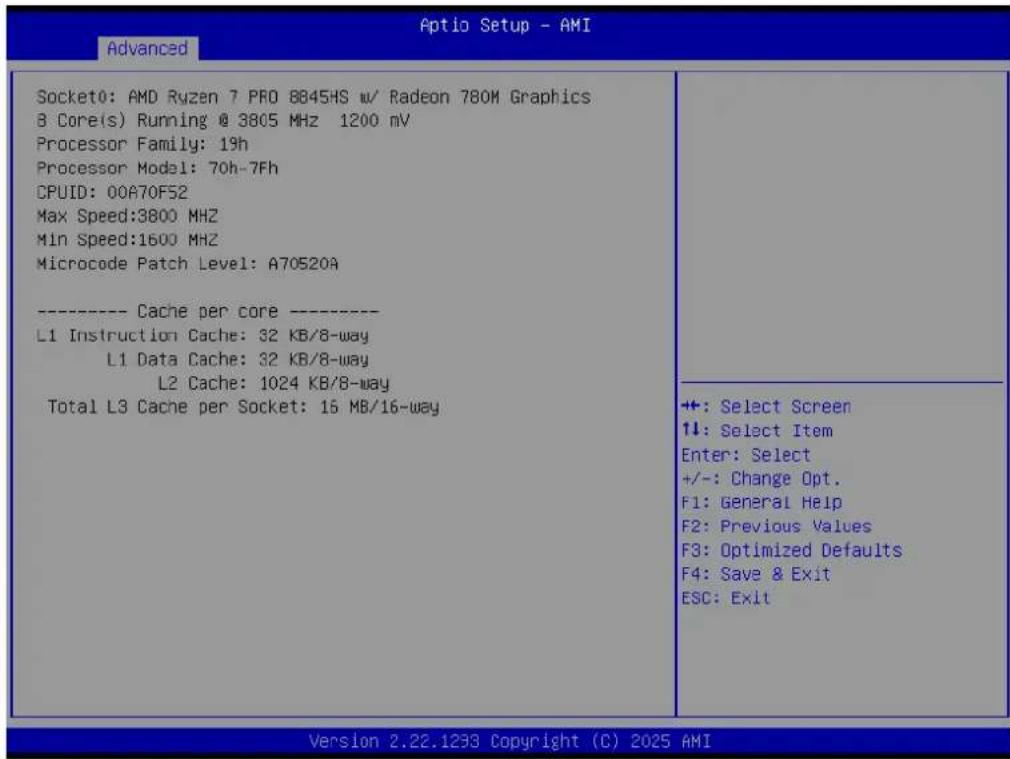
3.2.2.11 USB Configuration
Advanced → USB Configuration
| Advanced Aptio Setup - AMI | |
| USB Configuration USB Module Version 31 USB Controllers: 5 XHCIs USB Devices: 1 Drive, 1 Keyboard Legacy USB Support [Enabled] XHCI Hand-off [Enabled] USB Mass Storage Driver Support [Enabled] | Enables Legacy USB support. AUTO option disables legacy support if no USB devices are connected. DISABLE option will keep USB devices available only for EFI applications. |
| USB hardware delays and time-outs: USB transfer time-out [20 sec] Device reset time-out [20 sec] Device power-up delay [Auto] | +: Select Screen ↑↓: Select Item Enter: Select +/-: Change Opt. F1: General Help F2: Previous Values F3: Optimized Defaults F4: Save & Exit ESC: Exit |
| Mass Storage Devices: SRT USB 1100 [Auto] | |
| USB PWR OFF Configuration 1 [Disabled] USB PWR OFF Configuration 2 [Disabled] USB PWR OFF Configuration 3 [Disabled] | |
| Version 2.22.1233 Copyright (C) 2025 AMI | |
3.2.2.12 Network Stack Configuration
Advanced → Network Stack Configuration
![Advanced Aptio Setup - AMI Network Stack [Disabled] Enable/Disable UEFI Network Stack +: Select Screen 1: Select Item Enter: Select +/-: Change Opt. F1: General Help F2: Previous Values F3: Optimized Defaults F4: Save & Exit ESC: Exit Version 2.22.1233 Copyright (C) 2025 AMI](/content/2026/07/1486455/images/cf63538ecf8ceda46d2796a37fd6e58461774a87369478ca896e7de27ed9bd82.jpg)
3.2.2.13 NVMe Configuration
Advanced → NVMe Configuration
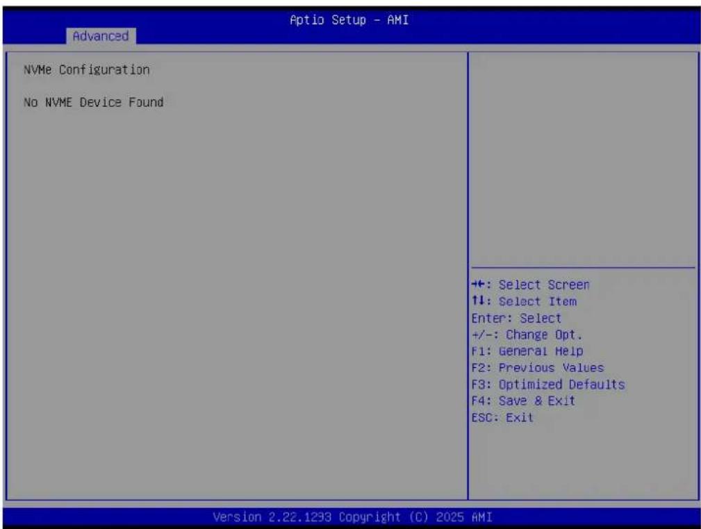
3.2.2.14 Asmedia AHCI Controller
Advanced → Asmedia AHCI Controller
![Optio Setup - AMI Advanced Asmedia AHCI Controller SATA Port 0 [Not Installed] SATA Port 1 [Not Installed] ++: Select Screen ↑↓: Select Item Enter: Select +/-: Change Opt. F1: General Help F2: Previous Values F3: Optimized Defaults F4: Save & Exit ESC: Exit Version 2.22.1233 Copyright (C) 2025 AMI](/content/2026/07/1486455/images/87c20322c9a229050d980a575140019474ed047adfade82cae15e2049fd45a7f.jpg)
3.2.3 Chipset Configuration Setting
Select the chipset tab from the BIOS setup screen to enter the Chipset Setup screen. Users can select any item in the left frame of the screen, such as PCI Express Configuration, to go to the sub-menu for that item. Users can display a Chipset Setup option by highlighting it using the
3.2.3.1 South Bridge
Chipset → South Bridge

PCI Express Configuration
Chipset → South Bridge → PCI Express Configuration
![Aptio Setup - AMI Chipset PCI Express Configuration PCIE Wake [Auto] PCIE Device Initial Delay 0 Restore AC Power Loss [Power Off] LAN1 Controller [Enabled] LAN1 PXE OpROM [Disabled] LAN2 Controller [Enabled] LAN2 PXE OpROM [Disabled] PCI Express Configuration Parameters ++: Select Screen ↑↓: Select…](/content/2026/07/1486455/images/5d71a6acb7b4fd10d542f131b7b65ea71fc269e1027d0c2eda6cac8b4ded94f6.jpg)
PCIEX16_1 Slot
Chipset → South Bridge → PCI Express Configuration → PCIEX16_1 Slot
![Aptio Setup - AMI Chipset PCI Express Configuration PCIEX16_1 Slot [Auto] PCIe to USB [Auto] ASPM Mode Control [Auto] M2_M2-key Slot [Auto] LAN1 Controller [Enabled] LAN2 Controller [Enabled] M2_E1-key Slot [Auto] ASPM Mode Control [Auto] PCIe to SATA [Auto] ASPM Mode Control [Auto] M2_M1-key Slot […](/content/2026/07/1486455/images/74afad16a2050dd8194ff0713cd3c7c74f3ffb1dfd4ca1540f3eff9dc69c5507.jpg)
3.2.3.2 GFX Configuration
Chipset → GFX Configuration
![Aptio Setup - AMI Chipset GFX Configuration Panel Type [Disabled] Backlight Signal Control [FWM] Backlight Control PWM 100 Backlight PWM Frequency Control [23.3 KHz] IGD - AmdGop Output Priority [Default] IGD - AmdGop Bootup Brightness 255 Level +: Select Screen ↑↓: Select Item Enter: Select +/-: Ch…](/content/2026/07/1486455/images/436cdd401f06b3201a89310f1146037a9d3d11bd181dc54dd4699800a6e563d7.jpg)
3.2.3.3 North Bridge
Chipset → North Bridge

Socket 0 Information
Chipset → North Bridge → Socket 0 Information

3.2.4 Security
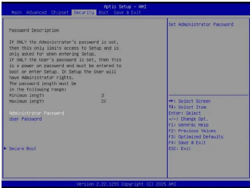
3.2.4.1 Secure Boot
Security → Secure Boot
![Aptio Setup - AMI Security System Mode Secure Boot Secure Boot Mode ►Restore Factory Keys ►Reset To Setup Mode ►Expert Key Management Setup [Enabled] Inactive [Standard] Secure Boot feature is Active if Secure Boot is Enabled, Platform Key(PK) is enrolled and the System is in User mode. The mode cha…](/content/2026/07/1486455/images/b6709b998a63ac44814ff6e8018a9ff9ad4edc86d5a10f36fd146ffbb4bfe6a9.jpg)
3.2.5 Boot Settings
![Aptio Setup - AMI Main Advanced Chipset Security Boot Save & Exit Boot Configuration Setup Prompt Timeout Bootup NumLock State Quiet Boot 1 [On] [Disabled] Boot Option Priorities Boot Option #1 [UEFI: SRT USB 1100, Partition 1 (SRT USB 1100)] Number of seconds to wait for setup activation key. 65535…](/content/2026/07/1486455/images/55b323d42b7fe70e0b7c94f006f7bdab27c88b48c5f416a28c56ccd8271562e3.jpg)
3.2.6 Save & Exit Configuration

Chapter 4
Software Introduction & Service
4.1 Introduction
The mission of Advantech Embedded Software Services is to "Enhance quality of life with Advantech platforms and Microsoft® Windows® embedded technology." We enable Windows® Embedded software products on Advantech platforms to more effectively support the embedded computing community. Customers are freed from the hassle of dealing with multiple vendors (hardware suppliers, system integrators, embedded OS distributors) for projects. Our goal is to make Windows® Embedded Software solutions easily and widely available to the embedded computing community.
4.2 Value-Added Software Services
Software API: An interface that defines the ways by which an application program may request services from libraries and/or operating systems. It provides not only the underlying drivers required but also a rich set of user-friendly, intelligent and integrated interfaces, which speeds development, enhances security, and offers add-on value for Advantech platforms. It plays the role of catalyst between developer and solution, and makes Advantech embedded platforms easier and simpler to adopt and operate with customer applications.
4.2.1 Software API
4.2.1.1 Control
GP I/O

General Purpose Input/Output is a flexible parallel interface that allows a variety of custom connections. It allows users to monitor the level of signal input or set the output status to switch on/off the device. Our API also provides Programmable GPIO, which allows developers to dynamically set the GPIO input or output status.
SMBus

SMBus is the System Management Bus defined by Intel Corporation in 1995. It is used in personal computers and servers for low-speed system management communications. The SMBus API allows a developer to interface with an embedded system environment and transfer serial messages using the SMBus protocols, allowing multiple simultaneous device control.
4.2.1.2 Display
Brightness Control

The Brightness Control API allows a developer to access embedded devices and easily control brightness.
Backlight

The Backlight API allows a developer to control the backlight (screen) on/off in embedded devices.
4.2.1.3 Monitor
Watchdog

A watchdog timer (WDT) is a device that performs a specific operation after a certain period of time if something goes wrong and the system does not recover on its own. A watchdog timer can be programmed to perform a warm boot (restarting the system) after a certain number of seconds.
Hardware Monitor

The Hardware Monitor (HWM) API is a system health supervision API that inspects certain condition indexes, such as fan speed, temperature, and voltage.
4.2.1.4 Power Saving
CPU Speed

Intel® SpeedStep® BIOS technology is utilized to save power. The system will automatically adjust the CPU speed depending on the system loading.
System Throttling

This refers to a series of methods for reducing power consumption in computers by lowering the clock frequency. This API allows the user to adjust the clock from 87.5% to 12.5%.
4.2.2 Software Utility
BIOS Flash

The BIOS Flash utility allows customers to update the flash ROM BIOS version, or use it to back up the current BIOS by copying it from the flash chip to a file on customers' disk. The BIOS Flash utility also provides a command line version and an API for fast implementation into customized applications.
Embedded Security ID

The embedded application is the most important property of a system integrator. It contains valuable intellectual property, design knowledge and innovation, but this makes it vulnerable! The Embedded Security ID utility provides reliable security functions for customers to secure their application data within the embedded BIOS.
Monitoring

Monitoring is a utility for customers to monitor aspects of system health, such as voltage, CPU and system temperature, and fan speed. These metrics are important to a device; if critical errors occur and are not solved immediately, permanent damage may be caused.
Chapter 5
Chipset Software Installation Utility
5.1 Before You Begin
To facilitate the installation of the enhanced display drivers and utility software, read the instructions in this chapter carefully. The drivers for the AIMB-2210 are located on the Advantech support website: http://support.advantech.com/Support/. The drivers on the support website will guide and link you to the utilities and drivers under a Windows system. Updates are provided via Service Packs from Microsoft*.
Note! The driver files on the website are compressed. Do not attempt to install the drivers by copying the files manually. You must download the files and decompress them first. Please use the supplied Setup program to install the drivers.
Before you begin, it is important to note that most display drivers need to have the relevant software application already installed in the system prior to installing the enhanced display drivers. In addition, many of the installation procedures assume that you are familiar with both the relevant software applications and operating system commands. Review the relevant operating system commands and the pertinent sections of your application software user manual before performing the installation.
5.2 Introduction
The Intel® Chipset Software Installation (CSI) utility installs the Windows INF files that outline to the operating system how the chipset components will be configured. This is needed for the proper functioning of the following features:
Core PCI PnP services
■ Serial ATA interface support
USB support
- Identification of Intel® chipset components in the Device Manager
Note! This utility is used for the following versions of Windows, and it has to be installed before installing all the other drivers:

Windows 10 (64-bit)
Chapter 6
LAN Configuration
6.1 Introduction
The AIMB-2210 system features dual Gigabit Ethernet LANs via dedicated PCI Express x1 lanes (RTL8111K (LAN1) and RTL8111K (LAN2)) that offer a bandwidth of up to 500 MB/sec, eliminating bottlenecks in the flow of network data by incorporating Gigabit Ethernet at 1000 Mbps. RTL8125BG (2.5GbE) is available by option.
6.2 Features
■ Integrated 10/100/1000/2500 Mbps transceiver
10/100/1000/2500 Mbps triple-speed MAC
■ High-speed RISC core with 24-KB cache
■ On-chip voltage regulation
■ Wake-on-LAN (WOL) support
■ PCI Express x1 host interface
6.3 Installation
Note! Before installing this driver, make sure the CSI utility has been installed in your system. See Chapter 5 for information on installing the CSI utility.
The RTL8111K (LAN1) and RTL8111K (LAN2) Gigabit integrated controllers support all major network operating systems. However, the installation procedure varies between systems. Please follow the driver setup procedure instructions specific to the operating system installed.
6.4 Windows® 11 Driver Setup (Realtek 8111G)
Download the driver from the support website on your computer and decompress the file. Select "Autorun", then navigate to the directory for your OS.
Note! Before installing this driver, make sure the CSI utility has been installed in your system. See Chapter 5 for information on installing the CSI utility.
www.advantech.com
Please verify specifications before quoting. This guide is intended for reference purposes only.
All product specifications are subject to change without notice.
No part of this publication may be reproduced in any form or by any means, such as electronically, by photocopying, recording, or otherwise, without prior written permission from the publisher.
All brand and product names are trademarks or registered trademarks of their respective companies.
© Advantech Co., Ltd. 2025
- AIMB-2210
- COPYRIGHT
- ACKNOWLEDGMENTS
- PRODUCT WARRANTY (2 YEARS)
- A MESSAGE TO THE CUSTOMER
- ADVANTECH CUSTOMER SERVICES
- TECHNICAL SUPPORT
- DECLARATION OF CONFORMITY
- FCC CLASS B
- MEMORY COMPATIBILITY
- ORDERING INFORMATION
- INITIAL INSPECTION
- CONTENTS
- CHAPTER 1 GENERAL INTRODUCTION ......1
- CHAPTER 2 CONNECTING PERIPHERALS ....13
- CHAPTER 3 BIOS OPERATION......47
- TABLE 3.1: CONTROL KEYS.... 48
- CHAPTER 4 SOFTWARE INTRODUCTION & SERVICE ..... 75
- CHAPTER 5 CHIPSET SOFTWARE INSTALLATION UTILITY 79
- CHAPTER 6 LAN CONFIGURATION 81
- CHAPTER 1
- 1.1 INTRODUCTION
- 1.2 FEATURES
- 1.3 SPECIFICATIONS
- 1.3.1 SYSTEM
- 1.3.2 MEMORY
- 1.3.3 INPUT/OUTPUT
- 1.3.4 GRAPHICS
- 1.3.5 ETHERNET LAN
- 1.3.6 INDUSTRIAL FEATURES
- 1.3.7 MECHANICAL AND ENVIRONMENTAL SPECIFICATIONS
- 1.4 JUMPERS AND CONNECTORS
- 1.5 BOARD LAYOUT: JUMPER AND CONNECTOR LOCATIONS
- 1.6 AIMB-2210 BOARD DIAGRAM
- 1.7 SAFETY PRECAUTIONS
- WARNING
- CAUTION
- 1.8 JUMPER SETTINGS
- 1.8.1 HOW TO SET JUMPERS
- 1.8.2 EDP PANEL / LVDS PANEL VOLTAGE SELECTION (JEDP1_LVDS1)
- 1.8.3 PWRBTN#/RESET# / HDD LED / INTERNAL BUZZER / EXTERNAL SPEAKER HEADER (JFP1)
- 1.8.4 COM1_RI# PIN RI#/5V/12V SELECTION (JSETCOM1_V1)
- 1.8.5 COM4_RI# PIN RI#/5V/12V SELECTION (JSETCOM4_V1)
- 1.8.6 AT/ATX MODE SELECTION (PSON1)
- 1.8.7 CASE OPEN STATE (NC/NO) SETTING PIN HEADER (JCASEOP_SW1)
- 1.8.8 MOS CLEAR JUMPER (JCMOS1)
- 1.8.9 COM3 CCTALK VOLTAGE SELECTION HEADER (JCCT_VCON1)
- 1.10 MEMORY INSTALLATION PROCEDURES
- CHAPTER 2
- 2.1 INTRODUCTION
- 2.2 I/O CONNECTOR
- 2.2.1 DUAL DISPLAYPORT (DP12)
- 2.2.2 DUAL DISPLAYPORT (DP34)
- 2.2.3 USB 3.1 STACK CONNECTOR * 2 PORTS (USB3_12)
- 2.2.4 USB 3.1 STACK CONNECTOR * 2 PORTS (USB_34)
- 2.2.5 RJ-45 SINGLE LAN PORT (LAN1)
- 2.2.6 RJ-45 SINGLE LAN PORT (LAN2)
- 2.2.7 M.2 E-KEY CONNECTOR (M2_E1)
- 2.2.8 M.2 M-KEY CONNECTOR (M2_M1)
- 2.2.9 M.2 M-KEY CONNECTOR (M2_M2)
- 2.2.10 12V POWER SUPPLY CONNECTOR (DCIN1)
- 2.2.11 SATA CONNECTOR (SATA1)
- 2.2.12 SATA CONNECTOR (SATA2)
- 2.2.13 PCIE X16 CONNECTOR (PCIEX16_1)
- 2.2.14 HD ANALOG AUDIO INTERFACE LINE-OUT (AUDIO1)
- 2.2.15 HD ANALOG AUDIO INTERFACE MIC-IN (AUDIO2)
- 2.2.16 DDR5 SODIMM SOCKET A1 (DIMMA1)
- 2.2.17 DDR5 SODIMM SOCKET B1 (DIMMB1)
- 2.3 BOX HEADER
- 2.3.1 EDP CONNECTOR / LVDS CONNECTOR (EDP1_LVDS1)
- 2.3.2 INTERNAL USB 2.0 CONNECTOR * 2 PORTS (USB56)
- 2.3.3 INTERNAL USB 2.0 CONNECTOR * 2 PORTS (USB78)
- 2.3.4 COM1 CONNECTOR (COM1)
- 2.3.5 COM2 CONNECTOR (COM2)
- 2.3.6 COM3 CONNECTOR (COM3)
- 2.3.7 COM4 CONNECTOR (COM4)
- 2.3.8 COM4 CONNECTOR (COM5)
- 2.3.9 COM4 CONNECTOR (COM6)
- 2.3.10 CMOS BATTERY CONNECTOR (BAT1)
- 2.3.11 EDP/LVDS BACKLIGHT INVERTER POWER CONNECTOR (INV1)
- 2.3.13 ATX 5V/PSON CONNECTOR (ATX_5VSB1)
- 2.3.14 SATA POWER CONNECTOR (SATA_PWR1)
- 2.3.15 SATA POWER CONNECTOR (SATA_PWR2)
- 2.4 PIN HEADER
- 2.4.1 POWER LED PIN HEADER (JFP2)
- 2.4.2 SPI BIOS FLASH SOCKET1 (SPI1)
- 2.4.3 SPI BIOS DEBUG HEADER (SPI_CN1)
- 2.4.4 8-BIT GENERAL PURPOSE I/O PIN HEADER (GPIO1)
- 2.4.5 8-BIT GENERAL PURPOSE I/O PIN HEADER (GPIO2)
- 2.4.6 CPU FAN CONNECTOR (CPUFAN1)
- 2.4.7 SYSTEM FAN CONNECTOR (SYSFAN1)
- 2.4.8 CASE OPEN CONNECTOR (JCASE1)
- 2.4.9 VCORE PROGRAMMING HEADER (VR_PMB1)
- 2.4.10 HD DIGITAL AUDIO INTERFACE S/PDIF OUT (SPDIF1)
- 2.4.11 AUDIO AMPLIFIER OUTPUT PIN HEADER (AMP1)
- 2.4.12 HD ANALOG AUDIO INTERFACE FRONT PANEL (FPAUD1)
- 2.5.5 PWRBTN# / RESET# / HDD LED / SERIAL BUS FROM HW MONITOR IC / INTERNAL BUZZER / EXTERNAL SPEAKER HEADER (JFP1)
- 2.5.6 CASE OPEN SIGNAL REVERSE HEADER (JCASEOP_SW1)
- 2.5.7 CMOS RESET HEADER (JCMOS1)
- 2.5.8 AT/ATX MODE SELECTION (PSON1)
- 3.2 BIOS SETUP
- 3.2.1 MAIN MENU
- SYSTEM TIME / SYSTEM DATA
- 3.2.2 ADVANCED BIOS FEATURES
- 3.2.2.1 TRUST COMPUTING
- 3.2.2.2 ACPI SETTINGS
- 3.2.2.3 AMD CBS
- CPU COMMON OPTIONS
- UMC COMMON OPTIONS
- DDR OPTIONS
- DDR RAS
- DDR ECC CONFIGURATION
- NBIO COMMON OPTIONS
- AUDIO CONFIGURATION
- FCH COMMON OPTIONS
- I3C/I2C CONFIGURATION OPTIONS
- SOC MISCELLANEOUS CONTROL
- 3.2.2.4 AMD PBS
- AMD FIRMWARE VERSION
- PCI EXPRESS CONFIGURATIONS
- 3.2.2.5 NCT6126D SUPER IO CONFIGURATION
- SERIAL PORT 1 CONFIGURATION
- SERIAL PORT 2 CONFIGURATION
- SERIAL PORT 3 CONFIGURATION
- SERIAL PORT 4 CONFIGURATION
- SERIAL PORT 5 CONFIGURATION
- SERIAL PORT 6 CONFIGURATION
- 3.2.2.6 NCT6126D HW MONITOR
- SMART FAN FUNCTION
- DIGITAL I/O CONFIGURATION
- 3.2.2.7 S5 RTC WAKE SETTINGS
- 3.2.2.8 UEFI VARIABLES PROTECTION
- 3.2.2.9 SERIAL PORT CONSOLE REDIRECTION
- 3.2.2.10 CPU CONFIGURATION
- NODE 0 INFORMATION
- 3.2.2.11 USB CONFIGURATION
- 3.2.2.12 NETWORK STACK CONFIGURATION
- 3.2.2.13 NVME CONFIGURATION
- 3.2.2.14 ASMEDIA AHCI CONTROLLER
- 3.2.3 CHIPSET CONFIGURATION SETTING
- 3.2.3.1 SOUTH BRIDGE
- PCI EXPRESS CONFIGURATION
- PCIEX16_1 SLOT
- 3.2.3.2 GFX CONFIGURATION
- 3.2.3.3 NORTH BRIDGE
- SOCKET 0 INFORMATION
- 3.2.4 SECURITY
- 3.2.4.1 SECURE BOOT
- 3.2.5 BOOT SETTINGS
- 3.2.6 SAVE & EXIT CONFIGURATION
- CHAPTER 4
- 4.1 INTRODUCTION
- 4.2 VALUE-ADDED SOFTWARE SERVICES
- 4.2.1 SOFTWARE API
- 4.2.1.1 CONTROL
- 4.2.1.2 DISPLAY
- 4.2.1.3 MONITOR
- 4.2.1.4 POWER SAVING
- 4.2.2 SOFTWARE UTILITY
- CHAPTER 5
- CHIPSET SOFTWARE INSTALLATION UTILITY
- 5.1 BEFORE YOU BEGIN
- 5.2 INTRODUCTION
- CHAPTER 6
- 6.1 INTRODUCTION
- 6.2 FEATURES
- 6.3 INSTALLATION
- 6.4 WINDOWS® 11 DRIVER SETUP (REALTEK 8111G)
- WWW.ADVANTECH.COM
Brand : Advantech
Model : AIMB-2210
Category : Motherboard