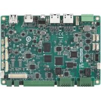
AFE-E420 - Electronic board Advantech - Free user manual and instructions
Find the device manual for free AFE-E420 Advantech in PDF.


| Product Type | Embedded Box PC |
| Brand | Advantech |
| Model | AFE-E420 |
| Dimensions (W x D x H) | 200 mm x 150 mm x 50 mm |
| Weight | 2.0 kg |
| Power Supply | 12V DC, 60W |
| Processor | Intel Core i5-7300U |
| Memory | 8 GB DDR4 (up to 32 GB) |
| Storage | 128 GB SSD (M.2 SATA) |
| Operating Temperature | -20°C to 60°C |
| Operating System Support | Windows 10 IoT, Linux Ubuntu |
| Connectivity | 2x Gigabit Ethernet, 4x USB 3.0, 2x COM |
| Expansion Slots | 1x Mini-PCIe, 1x M.2 2230 Key E |
| Display Output | 1x HDMI, 1x VGA |
| Cooling | Fanless design |
| Protection Rating | IP40 |
| Safety Certifications | CE, FCC, UL |
| Spare Parts Availability | Power adapter, fan kit, battery (RTC) |
| Repairability | Replaceable RAM, storage, wireless module |
| Maintenance | Clean with dry cloth; avoid moisture |
Frequently Asked Questions - AFE-E420 Advantech
User questions about AFE-E420 Advantech
0 question about this device. Answer the ones you know or ask your own.
Ask a new question about this device
Download the instructions for your Electronic board in PDF format for free! Find your manual AFE-E420 - Advantech and take your electronic device back in hand. On this page are published all the documents necessary for the use of your device. AFE-E420 by Advantech.
USER MANUAL AFE-E420 Advantech
AFE-E420
NXP® i.MX 93
Dual Arm® Cortex-A55 4" SBC
Copyright
The documentation and the software included with this product are copyrighted 2025 by Advantech Co., Ltd. All rights are reserved. Advantech Co., Ltd. reserves the right to make improvements in the products described in this manual at any time without notice. No part of this manual may be reproduced, copied, translated, or transmitted in any form or by any means without the prior written permission of Advantech Co., Ltd. The information provided in this manual is intended to be accurate and reliable. However, Advantech Co., Ltd. assumes no responsibility for its use, nor for any infringements of the rights of third parties that may result from its use.
Acknowledgments
Arm is a trademark of Arm Corporation.
NXP is a trademark of NXP Corporation.
All other product names or trademarks are properties of their respective owners.
For more information on this and other Advantech products, please visit our website: http://www.advantech.com
For technical support and service, please visit our support website at:
http://support.advantech.com
This manual is for the AFE-E420.
Part No. 2006E42000 Edition 1
Printed in China June 2025
Product Warranty (2 Years)
Advantech warrants the original purchaser that each of its products will be free from defects in materials and workmanship for two years from the date of purchase.
This warranty does not apply to any products that have been repaired or altered by persons other than repair personnel authorized by Advantech, or products that have been subject to misuse, abuse, accident, or improper installation. Advantech assumes no liability under the terms of this warranty as a consequence of such events.
Because of Advantech's high quality-control standards and rigorous testing, most customers never need to use our repair service. If an Advantech product is defective, it will be repaired or replaced free of charge during the warranty period. For out-of-warranty repairs, customers will be billed according to the cost of replacement materials, service time, and freight. Please consult your dealer for more details.
If you believe your product to be defective, follow the steps outlined below.
-
Collect all the information about the problem encountered. (For example, CPU speed, Advantech products used, other hardware and software used, etc.) Note anything abnormal and list any onscreen messages displayed when the problem occurs.
-
Call your dealer and describe the problem. Please have your manual, product, and any helpful information readily available.
-
If your product is diagnosed as defective, obtain a return merchandise authorization (RMA) number from your dealer. This allows us to process your return more quickly.
-
Carefully pack the defective product, a completed Repair and Replacement Order Card, and a proof of purchase date (such as a photocopy of your sales receipt) into a shippable container. Products returned without a proof of purchase date are not eligible for warranty service.
-
Write the RMA number clearly on the outside of the package and ship the package prepaid to your dealer.
Packing List
Before you begin installing your card, please make sure that the following materials have been shipped:
1 x AFE-E420 SBC
2 x M.2 screws
Optional Accessories
| Part Number Description | |
| 1700031582-01 RS-232 only Cable D-SUB 9P(M)/1*5P-1.25 20cm | |
| 1700035016-01 RS-422/485 Cable D-SUB 9P(M)/1x5P-1.25 20cm | |
| 1700019584-01 Audio Cable 2*5P-2.0/Audio JACK*3 20cm | |
| 1700030406-01 USB Cable 2*5P-2.0/USB-A 4P(F)*2 20cm | |
| 1700030405-01 GPIO Cable D-SUB 9P(F)/1*10P-1.25 20cm | |
| 1700030518-01 CAN Bus Cable D-SUB 9P(M)/1x5P-1.25 20cm | |
| EWM-C401CQE01 Cellular 4G M.2 3042 Key B, no SIM slot, no GNSS | |
| TBD Wi-Fi Module | |
| 96LCM-G070WV40L-A0 | 7" LCD, 400nits, 800x480 |
| 1700021883-01 | LVDS cable 1x20P-1.0/2x20P-1.25 50cm |
| 1700021882-01 | BKL cable 1x4P-1.25/1x5P-2.0 50cm |
Declaration of Conformity
CE
This product has passed the CE test for environmental specifications. Test conditions for passing included the equipment being operated within an industrial enclosure. In order to protect the product from being damaged by ESD (Electrostatic Discharge) and EMI leakage, we strongly recommend the use of CE-compliant industrial enclosure products.
FCC Class B
This equipment has been tested and found to comply with the limits for a Class B digital device, pursuant to part 15 of the FCC Rules. These limits are designed to provide reasonable protection against harmful interference in a residential installation. This equipment generates, uses, and can radiate radio frequency energy and, if not installed and used in accordance with the instruction manual, may cause harmful interference to radio communications. However, there is no guarantee that interference will not occur in a particular installation. If this equipment does cause harmful interference to radio or television reception, which can be determined by turning the equipment off and on, the user is encouraged to try to correct the interference by one or more of the following measures:
■ Reorient or relocate the receiving antenna.
■ Increase the separation between the equipment and receiver.
■ Connect the equipment into an outlet on a circuit different from that to which the receiver is connected.
- Consult the dealer or an experienced radio/TV technician for assistance.
Caution!

There is danger of a new battery exploding if it is incorrectly installed. Do not attempt to recharge, force open, or heat the battery. Replace the battery only with the same or equivalent type recommended by the manufacturer. Discard used batteries according to the manufacturer's instructions.
Technical Support and Assistance
- Visit the Advantech website at www.advantech.com/support to obtain the latest product information.
- Contact your distributor, sales representative, or Advantech's customer service center for technical support if you need additional assistance. Please have the following information ready before calling:
– Product name and serial number
– Description of your peripheral attachments
– Description of your software (operating system, version, application software, etc.)
– A complete description of the problem
– The exact wording of any error messages
Contents
Chapter 1 General Information ....1
1.1 Introduction ...... 2
1.2 Specifications 2
Table 1.1: Specifications ...... 2
1.3 Block Diagram....4
Chapter 2 Mechanical ....5
2.1 Board Layout: Dimensions 6
Figure 2.1 AFE-E420 Mechanical Drawing (Top Side)....6
Figure 2.2 AFE-E420 Mechanical Drawing (Bottom Side)....6
Figure 2.3 AFE-E420 Mechanical Drawing (Coastline) ..... 7
Chapter 3 Hardware Installation ......9
3.1 Jumpers & Switches.... 10
Table 3.1: Jumpers & Switches 10
3.2 Connectors.... 10
Table 3.2: Connector and Header List.... 10
3.3 Locating Connectors 11
Figure 3.1 AFE-E420 Connector Locations (Top Side) ..... 11
Figure 3.2 AFE-E420 Connector Locations (Bottom Side) ..... 11
3.4 Jumpers & Switches.... 12
3.4.1 Backlight Voltage Selection Jumper: LVDS_BKLT_SLT 12
Table 3.3: Backlight Voltage Selection Jumper: LVDS_BKLT_SLT 12
3.4.2 Auto Power On Selection Jumper: AT1 12
Table 3.4: Auto Power On Selection Jumper: AT1.... 12
3.4.3 USB Switch Jumper: J1 13
Table 3.5: USB Switch Jumper: J1.... 13
3.4.4 Panel Voltage Selection Jumper: LVDS_VDD_SLT 13
Table 3.6: Panel Voltage Selection Jumper: LVDS_VDD_SLT. 13
3.4.5 Boot Selection Switch: SW1 13
Table 3.7: Boot Selection Switch: SW1 13
3.4.6 CAN Bus Terminal Switch: CAN SW1 14
Table 3.8: CAN Bus Terminal Switch: CAN_SW1.... 14
3.4.7 CAN Bus Terminal Switch: CAN_SW2 14
Table 3.9: CAN Bus Terminal Switch: CAN_SW2....14
3.5 Connectors (Internal) 15
3.5.1 Control Pilot 1: CP1 15
Table 3.10: Control Pilot 1: CP1 15
3.5.2 Control Pilot 2: CP2 15
Table 3.11: Control Pilot 2: CP2 15
3.5.3 RTD Internal Connector: CN16.... 15
Table 3.12:RTD Internal Connector: CN16 15
3.5.4 Isolate COM Connector: ISO COM.... 16
Table 3.13:Isolate COM Connector: ISO_COM 16
3.5.5 Isolate CAN Connector: ISO CAN 17
Table 3.14: Isolate CAN Connector: ISO CAN 17
3.5.6 SPKR Connector: AMP1.... 17
Table 3.15:SPKR Connector: AMP1 17
3.5.7 Audio Internal Connector: AUDIO1.... 18
Table 3.16:Audio Internal Connector: AUDIO1 18
3.5.8 COM Port Connector: COMA .... 18 Table 3.17:COM Port Connector: COMA .... 18
3.5.9 COM Port Connector: COMB .... 19 Table 3.18:COM Port Connector: COMB .... 19
3.5.10 COM Port Connector: COMC 19 Table 3.19:COM Port Connector: COMC 19
3.5.11 COM Port Connector: COMD 20 Table 3.20:COM Port Connector: COMD 20
3.5.12 DC Power Input Connector (4-Pin): CN15.... 20 Table 3.21:DC Power Input Connector (4-Pin): CN15 .... 20
3.5.13 DC Power Input Connector (Phoenix): CN15 20 Table 3.22:DC Power Input Connector (Phoenix): CN15 20
3.5.14 POE Power Connector: POE_PWR1 .... 21 Table 3.23:POE Power Connector: POE_PWR1 .... 21
3.5.15 USB 2.0 Dual-Port Internal Connector: USB2 .... 21 Table 3.24:USB 2.0 Dual-Port Internal Connector: USB2.... 21
3.5.16 USB OTG Connector: USB0_OTG1.... 22 Table 3.25:USB OTG Connector: USB0_OTG1 .... 22
3.5.17 Internal Fan Connector: FAN1....22 Table 3.26:Internal Fan Connector: FAN1....22
3.5.18 Internal Fan Connector: FAN2.... 23 Table 3.27:Internal Fan Connector: FAN2 .... 23
3.5.19 CAN Bus Connector: CAN3....23 Table 3.28:CAN Bus Connector: CAN3....23
3.5.20 Front Panel Internal Connector: CN1 23 Table 3.29:Front Panel Internal Connector: CN1 23
3.5.21 CAN Bus Connector: CAN4.... 24 Table 3.30:CAN Bus Connector: CAN4 .... 24
3.5.22 GPIO Internal Connector: GPIO1 24 Table 3.31:GPIO Internal Connector: GPIO1 24
3.5.23 I2C Connector: I2C1.... 25 Table 3.32:I2C Connector: I2C1.... 25
3.5.24 I2C Connector: I2C2.... 26 Table 3.33:I2C Connector: I2C2.... 26
3.5.25 GPIO Internal Connector: GPIO2 26 Table 3.34:GPIO Internal Connector: GPIO2 26
3.5.26 Panel Inverter Connector: LVDS_BKLT_PWR.... 27 Table 3.35:Panel Inverter Connector: LVDS_BKLT_PWR.... 27
3.5.27 LVDS Connector: LVDS 27 Table 3.36:LVDS Connector: LVDS 27
3.5.28 RTC Battery Connector: BAT1 .... 29 Table 3.37:RTC Battery Connector: BAT1 .... 29
3.5.29 M.2 E-Key Connector: M2E_CN1.... 29 Table 3.38:M.2 E-Key Connector: M2E_CN1 .... 29
3.5.30 M.2 B-Key Connector: M2B_CN1.... 31 Table 3.39:M.2 B-Key Connector: M2B_CN1 .... 31
Chapter 4 Software Functionality ...... 35
4.1 User Guide.... 36
4.2 Test Functions 36
4.2.1 CPU 36
4.2.2 DDR.... 36
4.2.3 SD Card.... 37
4.2.4 eMMC 37
4.2.5 RS-232.... 37
4.2.6 RS-485/422.... 38
4.2.7 GPIO.... 40
4.2.8 M.2 (B-Key) 4G.... 40
4.2.9 M.2 (E-Key) Wi-Fi & BT 41
4.2.10 Ethernet 41
4.2.11 USB....41
4.2.12 Micro-USB OTG 41
4.2.13 HDMI....41
4.2.14 LVDS....41
4.2.15 I2C 42
4.2.16 RTC.... 42
4.2.17 PWM 43
4.2.18 Audio.... 43
4.2.19 Watchdog.... 44
4.2.20 ADC 44
4.2.21 RTD 45
4.2.22 PLC 45
4.2.23 CAN Bus 46
4.2.24 Fan.... 46
4.2.25 POE 47
Chapter 1
General Information
This chapter gives background information on the AFE-E420
Sections include:
Introduction
Specifications
Block diagram
1.1 Introduction
The AFE-E420 is a compact 4" SBC (single board computer) in the 165 x 115 mm form factor. It's part of the Compact Series and runs on the NXP® i.MX 93 processor, featuring a Dual Arm® Cortex-A55 core.
The AFE-E420 supports onboard LPDDR4x-3733 memory up to 2GB, and includes eMMC storage along with an SD card socket. Display options include either LVDS or HDMI.
For connectivity and I/O, it offers dual Gigabit Ethernet, three USB ports, six COM ports, four CAN bus interfaces, two PLC connections, and a 4-channel RTD input.
1.2 Specifications
| Table 1.1: Specifications | ||
| Platform | Processor NXP i.MX 93 with Dual Arm® Cortex-A55 | |
| Max. Frequency 1.70 GHz | ||
| Core Dual | ||
| Memory | Technology LPDDR4x-3733MT/s | |
| Max. Capacity Up to 2GB | ||
| Channel/Socket Single Channel / Onboard LPDDR4x | ||
| ECC Support Inline ECC | ||
| Display I/F | LCD | 1 x LVDS, Single Channel 18-/24-bit, up to 1366 x 768 or 1280 x 800 (*other LVDS panel) |
| *HDMI | 1 x HDMI 1.3, up to 1920 x 1080 (*HDMI support by request) | |
| Display | Single Display, LVDS or HDMI | |
| Ethernet | Controller | 2 x LAN: Realtek 8211 (PHY) |
| Speed | GbE | |
| External I/O | Ethernet | 2 x RJ-45 |
| HDMI | *1 | |
| USB 2.0 | 1 | |
| Micro-USB | 1 (for debug only) | |
| Internal I/O | USB 2.0 | 2 |
| Serial Bus 2 x I2C | ||
| COM Port | 6 x RS-232/422/485 (COM5 & COM6 with isolation) | |
| GPIO | 16-bit general purpose input output | |
| CAN Bus | 4 x CAN-FD (CAN1 & CAN2 with isolation) | |
| Audio | NXP SGTL5000, Line-in/Line-out/MIC | |
| Amplifier | YES (Stereo, 2.5W) | |
| RTD | 4-channel (3-wire), PT1000/PT100 compatible sampling rate 100Hz | |
| Fan | 2 x fans, 12V, 0.3A (4-wire) | |
| Front Panel Control | Power Button, Reset Button, 5V/3.3V Power Indicator | |
| Power Line Communication | PLC Controller | 2 x QCA7006 |
| Control Pilot | Dual ports with PWM & ADC | |
| Storage | eMMC | 16 GB |
Table 1.1: Specifications
| Expansion | M.2 E-Key 1 x E-Key 2230 (SDHC x1, UART x1) | |
| M.2 B-Key 1 x B-Key 3042 (USB 2.0 x1) w/ Nano-SIM | ||
| SD Card 1 x SD slot | ||
| Power | Supply Voltage | Vin: DC 12~24V +/- 10%;RTC Battery: Lithium 3V/210mAh |
| Connector 2-pin Phoenix connector, optional ATX 2x2pin 180D | ||
| Power Management | AT, ATX | |
| Max. Consumption TBU | ||
| Idle Consumption TBU | ||
| Environment | Temperature | Operating: Standard: 0 ~ 60°C (32 ~ 140°F) for HDMI with 0.7m/s airflowExtend: -40 ~ 85°C (-40 ~ 185°F) for LVDS with 0.7m/s airflowStorage: -40 ~ 85°C (-40 ~ 185°F) |
| Humidity | Operating: 40°C @ 95% relative humidity, non-condensingStorage: 60°C @ 95% relative humidity, non-condensing | |
| Vibration Resistance | 3.5 Grms | |
| Certification EMC CE, FCC Class B | ||
| Mechanical | Dimensions 165 x 115 mm (6.5" x 4.5") | |
| Net Weight 150 g | ||
*Note: Support by request
1.3 Block Diagram
![graph TD A["LPDDR4x Up to 2GB"] --> B["NXP i.MX93"] C["PMIC PCA9451"] --> B D["BKLT PWR & CTRL"] --> B E["LVDS"] --> B F["HDMI"] --> G["ADV7535"] H["USB2.0"] --> I["GL852"] J["2x USB2.0"] --> K["SIM Holder"] L["M.2 B-Key 3042/3052"] --> K M["M.2 E-Key 2230"] --> N["eMMC5.1"] O["SD Card"] --> P["Micr…](/content/2026/07/1458238/images/fd5efcf8c02dd58893b1c242e6b0f843c42d0d979fc8e2eb7b9f4c93b5a27395.jpg)
Chapter 2
Mechanical
This chapter gives mechanical information on the AFE-E420
Sections include:
■ Mechanical Drawings
2.1 Board Layout: Dimensions

Figure 2.1 AFE-E420 Mechanical Drawing (Top Side)
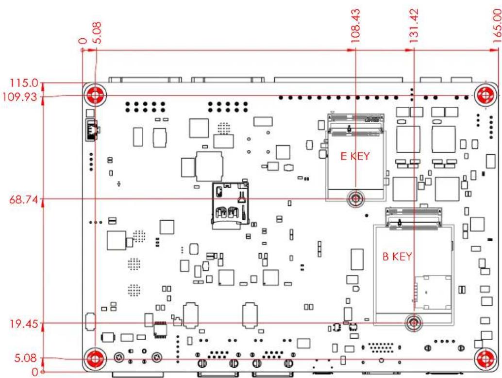
Figure 2.2 AFE-E420 Mechanical Drawing (Bottom Side)

Figure 2.3 AFE-E420 Mechanical Drawing (Coastline)
Chapter 3
Hardware Installation
This chapter explains the setup procedures for the AFE-E420 hardware, including instructions on setting jumpers and connecting peripherals, switches, and indicators. Be sure to read all safety precautions before you begin the installation procedure.
3.1 Jumpers & Switches
The AFE-E420 has a number of jumpers that allow you to configure your system to suit your application. The table below lists the functions of the various jumpers.
Table 3.1: Jumpers & Switches
| LVDS_BKLT_SLT Backlight Voltage Selection Jumper |
| AT1 Auto Power On Selection Jumper |
| J1 USB Switch Jumper |
| LVDS_VDD_SLT Panel Voltage Selection Jumper |
| SW1 BOOT Selection Switch |
| CAN_SW1 CAN Bus Terminal Switch |
| CAN_SW2 CAN Bus Terminal Switch |
3.2 Connectors
Onboard connectors link the AFE-E420 to external devices such as hard disk drives and a keyboard. The table below lists the function of each of the board's connectors.
Table 3.2: Connector and Header List
| No Location name | Description | |
| 1 | CP1 | Control Pilot 1 |
| 2 | CP2 | Control Pilot 2 |
| 3 | CN16 | RTD Connector |
| 4 | AMP1 | SPKR Connector |
| 5 | AUDIO1 | Audio Internal Connector |
| 6 | AT1 | Auto Power On Selection Jumper |
| 7 | ISO_COM | Isolate COM Connector |
| 8 | COMA | COM Port Connector |
| 9 | COMB | COM Port Connector |
| 10 | COMC | COM Port Connector |
| 11 | COMD | COM Port Connector |
| 12 | CN15 | DC Power Input Connector (4-pin) |
| 13 | DCIN1 | DC Power Input Connector (Phoenix) |
| 14 | POE_PWR1 | POE Power Connector |
| 15 | LAN1 | RJ-45 Connector |
| 16 | LAN2 | RJ-45 Connector |
| 17 | USB1 | USB 2.0 Connector |
| 18 | USB2 | USB 2.0 Internal Connector |
| 19 | USB0_OTG1 USB OTG Connector | |
| 20 | J1 | USB Switch Jumper |
| 21 | HDMI | HDMI Connector |
| 22 | FAN1 | FAN Internal Connector |
| 23 | FAN2 | FAN Internal Connector |
| 24 | ISO_CAN | Isolate CAN Bus Connector |
| 25 | CAN3 | CAN Bus Connector |
| 26 | CAN4 | CAN Bus Connector |
| 27 | CN1 | Front Panel Internal Connector |
| 28 | GPIO1 | GPIO Connector |
| 29 | GPIO2 | GPIO Connector |
Table 3.2: Connector and Header List
| 30 I2C1 I2C Connector |
| 31 I2C2 I2C Connector |
| 32 LVDS_BKLT_SLT Backlight Voltage Selection Jumper |
| 33 LVDS_BKLT_PWR Panel Inverter Connector |
| 34 LVDS_VDD_SLT Panel Voltage Selection Jumper |
| 35 LVDS LVDS Connector |
| 36 BAT1 RTC battery Connector |
| 37 M2E_CN1 M.2 E-Key Connector |
| 38 SD_CARD1 SD Card Connector |
| 39 M2B_CN1 M.2 B-Key Connector |
| 40 SIM1 NANO SIM |
3.3 Locating Connectors

Figure 3.1 AFE-E420 Connector Locations (Top Side)

Figure 3.2 AFE-E420 Connector Locations (Bottom Side)
3.4 Jumpers & Switches
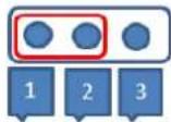
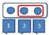
You may configure your card to match the needs of your application by setting jumpers. A jumper is a metal bridge used to close an electric circuit. It consists of two metal pins and a small metal clip (often protected by a plastic cover) that slides over the pins to connect them. To "close" a jumper, you connect the pins with the clip. To "open" a jumper, you remove the clip. Sometimes a jumper will have three pins, labeled 1, 2 and 3. In this case you would connect either pins 1 and 2, or 2 and 3.
The jumper settings are schematically depicted in this manual as follows:

A pair of needle-nose pliers may be helpful when working with jumpers. If you have any doubts about the best hardware configuration for your application, contact your local distributor or sales representative before you make any changes. Generally, you simply need a standard cable to make most connections.
3.4.1 Backlight Voltage Selection Jumper: LVDS_BKLT_SLT
Table 3.3: Backlight Voltage Selection Jumper: LVDS_BKLT_SLT
Jumper Short Backlight Voltage
| 1-2 | +V5 |
| 2-3 | +V12 (Default) |


3.4.2 Auto Power On Selection Jumper: AT1
Table 3.4: Auto Power On Selection Jumper: AT1
Jumper Short Functional
| 1-2 | Push-button Power On (ATX) |
| 2-3 | Auto Power On (Default) |

3.4.3 USB Switch Jumper: J1
Table 3.5: USB Switch Jumper: J1
| Jumper Short Functional | |
| 1-3 | USB to UART |
| 2-4 | (FT4232HQ)(Default) |
| 3-5 | Micro-USB |
| 4-6 | USB1_OTG |

3.4.4 Panel Voltage Selection Jumper: LVDS_VDD_SLT
Table 3.6: Panel Voltage Selection Jumper: LVDS_VDD_SLT
| Jumper Short Panel Voltage |
| 1-2 +V3.3 (Default) |
| 2-3 +V5 |
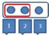
3.4.5 Boot Selection Switch: SW1
Table 3.7: Boot Selection Switch: SW1
| Pin1 Pin2 |
| SD card ON ON |
| eMMC OFF ON |
| Serial download ON OFF |

3.4.6 CAN Bus Terminal Switch: CAN_SW1
Table 3.8: CAN Bus Terminal Switch: CAN_SW1
| SWITCH Function |
| On Enable 124ohm Terminal |
| Off Disable 124ohm Terminal |

3.4.7 CAN Bus Terminal Switch: CAN_SW2
Table 3.9: CAN Bus Terminal Switch: CAN_SW2
| SWITCH Function |
| On Enable 124ohm Terminal |
| Off Disable 124ohm Terminal |

3.5 Connectors (Internal)
3.5.1 Control Pilot 1: CP1
Table 3.10: Control Pilot 1: CP1
| Pin Signal Pin Definition |
| 1 PILOT_OUT_1 |
| 2 PLC_CE_1 |

3.5.2 Control Pilot 2: CP2
Table 3.11: Control Pilot 2: CP2
| Pin Signal Pin Definition |
| 1 PILOT_OUT_2 |
| 2 PLC_CE_2 |

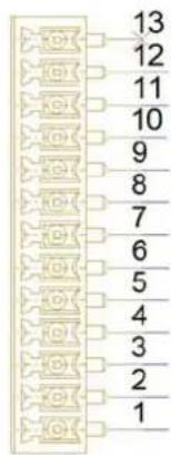
3.5.3 RTD Internal Connector: CN16
Table 3.12: RTD Internal Connector: CN16
| Pin Signal Pin Definition |
| 1 RTD1_PL1 |
| 2 RTD1_PL2 |
| 3 RTD12_RL3 |
| 4 RTD2_PL1 |
| 5 RTD2_PL2 |
| 6 RTD12_RL3 |
| 7 RTD3_PL1 |
| 8 RTD3_PL2 |
| 9 RTD34_RL3 |
| 10 RTD4_PL1 |
| 11 RTD4_PL2 |
| 12 RTD34_RL3 |
| 13 NC |
3.5.4 Isolate COM Connector: ISO_COM
Table 3.13: Isolate COM Connector: ISO_COM
| Pin RS232 RS422 RS485 |
| 1 RXD TX+ DAT+ |
| 2 RXD TX+ DT+ |
| 3 RTS RX- |
| 4 RTS RX- |
| 5 TXD RX+ |
| 6 TXD RX+ DAT- |
| 7 CTS TX- DAT- |
| 8 CTS TX- |
| 9 GND |
| 10 GND |

3.5.5 Isolate CAN Connector: ISO_CAN
Table 3.14: Isolate CAN Connector: ISO_CAN
| Pin Signal Pin Definition | |
| 1 | NC |
| 2 | NC |
| 3 GND_CAN | |
| 4 GND_CAN | |
| 5 CANA_L | |
| 6 CANB_L | |
| 7 CANA_H | |
| 8 CANB_H | |
| 9 | NC |
| 10 NC | |

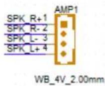
3.5.6 SPKR Connector: AMP1
Table 3.15: SPKR Connector: AMP1
| Pin Signal Pin Definition |
| 1 SPK_R+ |
| 2 SPK_R- |
| 3 SPK_L- |
| 4 SPK_L+ |
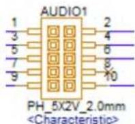
3.5.7 Audio Internal Connector: AUDIO1
Table 3.16: Audio Internal Connector: AUDIO1
Pin Signal Pin Definition
| 1 LINEOUT_L | |
| 2 LINEIN_R | |
| 3 AGND | |
| 4 AGND | |
| 5 LINEOUT_R | |
| 6 LINEIN_L | |
| 7 AGND | |
| 8 | NC |
| 9 MIC_IN | |
| 10 MIC_IN | |
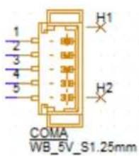
3.5.8 COM Port Connector: COMA
Table 3.17: COM Port Connector: COMA
Pin RS232 RS422 RS485
| 1 TXD RX+ |
| 2 RTS RX- |
| 3 RXD TX+ DAT+ |
| 4 CTS TX- DAT- |
| 5 GND |
3.5.9 COM Port Connector: COMB
Table 3.18: COM Port Connector: COMB
| Pin RS232 RS422 RS485 |
| 1 TXD RX+ |
| 2 RTS RX- |
| 3 RXD TX+ DAT+ |
| 4 CTS TX- DAT- |
| 5 GND |

3.5.10 COM Port Connector: COMC
Table 3.19: COM Port Connector: COMC
| Pin RS232 RS422 RS485 |
| 1 TXD RX+ |
| 2 RTS RX- |
| 3 RXD TX+ DAT+ |
| 4 CTS TX- DAT- |
| 5 GND |

3.5.11 COM Port Connector: COMD
Table 3.20: COM Port Connector: COMD
Pin RS232 RS422 RS485
| 1 TXD RX+ |
| 2 RTS RX- |
| 3 RXD TX+ DAT+ |
| 4 CTS TX- DAT- |
| 5 GND |

3.5.12 DC Power Input Connector (4-Pin): CN15
Table 3.21: DC Power Input Connector (4-Pin): CN15
| Pin Signal Pin Definition |
| 1 GND |
| 2 GND |
| 3 +VIN_DCIN |
| 4 +VIN_DCIN |

3.5.13 DC Power Input Connector (Phoenix): CN15
Table 3.22: DC Power Input Connector (Phoenix): CN15
| Pin Signal Pin Definition |
| 1 GND |
| 2 +VIN_DCIN |

3.5.14 POE Power Connector: POE_PWR1
Table 3.23: POE Power Connector: POE_PWR1
| Pin Signal Pin Definition |
| 1 +V48_LAN2+ |
| 2 +V48_LAN2- |
| 3 +V48_LAN3+ |
| 4 +V48_LAN3- |
| 5 GND |
| 6 +VDCIN |

3.5.15 USB 2.0 Dual-Port Internal Connector: USB2
Table 3.24: USB 2.0 Dual-Port Internal Connector: USB2
| Pin Signal Pin Definition |
| 1 +V5_USB2_C |
| 2 +V5_USB3_C |
| 3 USB2_DN_C |
| 4 USB3_DN_C |
| 5 USB2_DP_C |
| 6 USB3_DP_C |
| 7 GND |
| 8 GND |
| 9 GND |
| 10 NC |

3.5.16 USB OTG Connector: USB0_OTG1
Table 3.25: USB OTG Connector: USB0_OTG1
Pin Signal Pin Definition
| 1 +V5_USBOTG_C |
| 2 USBA_DN_C |
| 3 USBA_DP_C |
| 4 USB_A_ID_C |
| 5 GND |

3.5.17 Internal Fan Connector: FAN1
Table 3.26: Internal Fan Connector: FAN1
Pin Signal Pin Definition
| 1 GND |
| 2 +V12 |
| 3 FAN1_SPEED |
| 4 FAN1_V5_PWM |

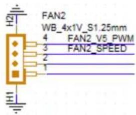
3.5.18 Internal Fan Connector: FAN2
Table 3.27: Internal Fan Connector: FAN2
| Pin Signal Pin Definition |
| 1 GND |
| 2 +V12 |
| 3 FAN2_SPEED |
| 4 FAN2_V5_PWM |
3.5.19 CAN Bus Connector: CAN3
Table 3.28: CAN Bus Connector: CAN3
| Pin Signal Pin Definition |
| 1 CAN3_H |
| 2 CAN3_L |
| 3 GND |

3.5.20 Front Panel Internal Connector: CN1
Table 3.29: Front Panel Internal Connector: CN1
| Pin Signal Pin Definition | |
| 1 GND | |
| 2 | NC |
| 3 | NC |
| 4 | NC |
| 5 | NC |
| 6 FP_a_PSIN# | |
| 7 SYS_RST# | |
| 8 +V3.3 | |
| 9 | NC |
| 10 +V5 | |

3.5.21 CAN Bus Connector: CAN4
Table 3.30: CAN Bus Connector: CAN4
Pin Signal Pin Definition
| 1 CAN4_H |
| 2 CAN4_L |
| 3 GND |

3.5.22 GPIO Internal Connector: GPIO1
Table 3.31: GPIO Internal Connector: GPIO1
| Pin Signal Pin Definition |
| 1 GND |
| 2 GPIO_A_7 |
| 3 GPIO_A_2 |
| 4 GPIO_A_6 |
| 5 GPIO_A_1 |
| 6 GPIO_A_5 |
| 7 GPIO_A_0 |
| 8 GPIO_A_4 |
| 9 +V3.3_P1_GPIO |
| 10 GPIO_A_3 |

3.5.23 I2C Connector: I2C1
Table 3.32: I2C Connector: I2C1
| Pin Signal Pin Definition |
| 1 GND |
| 2 I2C2_SDA |
| 3 I2C2_SCL |
| 4 +V3.3_I2CCONN1 |

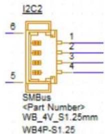
3.5.24 I2C Connector: I2C2
Table 3.33: I2C Connector: I2C2
Pin Signal Pin Definition
| 1 GND |
| 2 I2C3_SDA |
| 3 I2C3_SCL |
| 4 +V3.3_I2CCONN2 |
3.5.25 GPIO Internal Connector: GPIO2
Table 3.34: GPIO Internal Connector: GPIO2
Pin Signal Pin Definition
| 1 GND |
| 2 GPIO_B_7 |
| 3 GPIO_B_2 |
| 4 GPIO_B_6 |
| 5 GPIO_B_1 |
| 6 GPIO_B_5 |
| 7 GPIO_B_0 |
| 8 GPIO_B_4 |
| 9 +V3.3_P2_GPIO |
| 10 GPIO_B_3 |

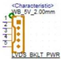
3.5.26 Panel Inverter Connector: LVDS_BKLT_PWR
Table 3.35: Panel Inverter Connector: LVDS_BKLT_PWR
| Pin Signal Pin Definition |
| 1 +VDD_BKLT |
| 2 GND |
| 3 LVDS_BL_EN |
| 4 LVDS_BL_PWM |
| 5 +V5 |
3.5.27 LVDS Connector: LVDS
Table 3.36: LVDS Connector: LVDS
| Pin Signal Pin Definition | |
| 1 +VDD_LVDS | |
| 2 +VDD_LVDS | |
| 3 GND | |
| 4 GND | |
| 5 +VDD_LVDS | |
| 6 +VDD_LVDS | |
| 7 LVDS_A_LANE0_N | |
| 8 NC | |
| 9 LVDS_A_LANE0_P | |
| 10 NC | |
| 11 GND | |
| 12 GND | |
| 13 LVDS_A_LANE1_N | |
| 14 NC | |
| 15 LVDS_A_LANE1_P | |
| 16 NC | |
| 17 GND | |
| 18 GND | |
| 19 LVDS_A_LANE2_N | |
| 20 NC | |
| 21 LVDS_A_LANE2_P | |
| 22 NC | |
| 23 GND | |
| 24 GND | |
| 25 LVDS_A_CLK_N | |
| 26 NC |
Table 3.36: LVDS Connector: LVDS
| 27 LVDS_A_CLK_P |
| 28 NC |
| 29 GND |
| 30 GND |
| 31 I2C_SCL_LVDS |
| 32 I2C_SDA_LVDS |
| 33 GND |
| 34 GND |
| 35 LVDS_A_LANE3_N |
| 36 NC |
| 37 LVDS_A_LANE3_P |
| 38 NC |
| 39 NC |
| 40 LVDS_CTRL |
| 41 NC |
| 42 NC |
| 43 NC |
| 44 NC |

3.5.28 RTC Battery Connector: BAT1
Table 3.37: RTC Battery Connector: BAT1
| Pin Signal Pin Definition |
| 1 +VBAT_b1 |
| 2 GND |

3.5.29 M.2 E-Key Connector: M2E_CN1
Table 3.38: M.2 E-Key Connector: M2E_CN1
| Pin Signal Pin Definition | |
| 1 GND | |
| 2 +V3.3_M2E | |
| 3 | NC |
| 4 +V3.3_M2E | |
| 5 | NC |
| 6 LED_OUT_WLAN# | |
| 7 GND | |
| 8 | NC |
| 9 SD3_CLK | |
| 10 NC | |
| 11 SD3_CMD | |
| 12 NC | |
| 13 SD3_DATA0 | |
| 14 NC | |
| 15 SD3_DATA1 | |
| 16 LED_OUT_BT# | |
| 17 SD3_DATA2 | |
| 18 GND | |
| 19 SD3_DATA3 | |
| 20 M2E_UR_WAKE# | |
| 21 M2_SDIO_WAKE# | |
| 22 UART5_RXD | |
| 23 M2_SDIO_RST# | |
| 32 UART5_TXD | |
| 33 GND | |
| 34 UART5_CTS | |
| 35 NC | |
| 36 UART5_RTS | |
Table 3.38: M.2 E-Key Connector: M2E_CN1
| 37 NC |
| 38 NC |
| 39 GND |
| 40 NC |
| 41 NC |
| 42 NC |
| 43 NC |
| 44 NC |
| 45 GND |
| 46 NC |
| 47 NC |
| 48 NC |
| 49 NC |
| 50 M2_SYSCLK_R |
| 51 GND |
| 52 M2E_RST# |
| 53 NC |
| 54 M2E_W_DISABLE2#_C |
| 55 NC |
| 56 M2E_W_DISABLE1#_C |
| 57 GND |
| 58 I2C_A_SDA |
| 59 NC |
| 60 I2C_A_SCL |
| 61 NC |
| 62 M2E_nALERT_C |
| 63 GND |
| 64 NC |
| 65 NC |
| 66 NC |
| 67 NC |
| 68 NC |
| 69 GND |
| 70 NC |
| 71 NC |
| 72 +V3.3_M2E |
| 73 NC |
| 74 +V3.3_M2E |
| 75 GND |
| H1 NC |
| H2 NC |
| H3 GND |
| H4 GND |
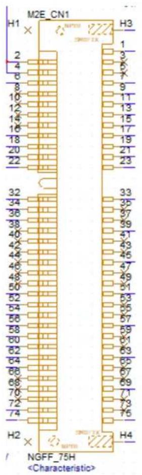
3.5.30 M.2 B-Key Connector: M2B_CN1
Table 3.39: M.2 B-Key Connector: M2B_CN1
| Pin Signal Pin Definition | |
| 1 | NC |
| 2 +V3.8 | |
| 3 GND | |
| 4 +V3.8 | |
| 5 GND | |
| 6 M2B_POWER_OFF# | |
| 7 USB_M2B_DP | |
| 8 M2B_W_DISABLE1# | |
| 9 USB_M2B_DN | |
| 10 LED_M2B# | |
| 11 GND | |
| 20 NC | |
| 21 NC | |
| 22 NC | |
| 23 NC | |
| 24 NC | |
| 25 M2B_DPR | |
Table 3.39: M.2 B-Key Connector: M2B_CN1
| 26 M2B_W_DISABLE2# |
| 27 GND |
| 28 NC |
| 29 NC |
| 30 UIM_A_RESET |
| 31 NC |
| 32 UIM_A_CLK |
| 33 GND |
| 34 UIM_A_DATA |
| 35 NC |
| 36 +VUIM_PWR |
| 37 NC |
| 38 NC |
| 39 GND |
| 40 NC |
| 41 NC |
| 42 NC |
| 43 NC |
| 44 M2B_ALERT# |
| 45 GND |
| 46 NC |
| 47 NC |
| 48 NC |
| 49 NC |
| 50 NC |
| 51 GND |
| 52 M2B_CLKREQ# |
| 53 NC |
| 54 M2B_WAKE# |
| 55 NC |
| 56 NC |
| 57 GND |
| 58 NC |
| 59 M2B_ANTCTL0 |
| 60 NC |
| 61 NC |
| 62 NC |
| 63 NC |
| 64 NC |
| 65 NC |
| 66 SIM_DETECT |
| 67 M2B_RST# |
| 68 NC |
| 69 NC |
| 70 +V3.8 |
| 71 GND |
| 72 +V3.8 |
Table 3.39: M.2 B-Key Connector: M2B_CN1
| 73 GND |
| 74 +V3.8 |
| 75 NC |
| H1 NC |
| H2 NC |
| H3 GND |
| H4 GND |

Chapter 4
Software Functionality
4.1 User Guide
For detailed operating instructions, please refer to the Yocto Linux BSP Version A User Guide. The following link directs you to the Imx93 series Wikipedia page: ess-wiki.advantech.com.tw/view/IoTGateway/BSP/Linux/iMX93/Yocto_LBVA_User_Guide
4.2 Test Functions
4.2.1 CPU
\$ cat /proc/cpuinfo
processor : 0
BogoMIPS : 48.00
Features : fp asimd evtstrm aes pmull sha1 sha2 crc32 atomics fphp asimdhp cpuid asimdrdm lrcpc dcpop asimddp
CPU implementer : 0x41
CPU architecture: 8
CPU variant : 0x2
CPU part : 0xd05
CPU revision : 0
processor : 1
BogoMIPS : 48.00
Features : fp asimd evtstrm aes pmull sha1 sha2 crc32 atomics fphp asimdhp cpuid asimdrdm lrcpc dcpop asimddp
CPU implementer : 0x41
CPU architecture: 8
CPU variant : 0x2
CPU part : 0xd05
CPU revision : 0
4.2.2 DDR
\$ cat /proc/meminfo
VmallocUsed: 6472 kB
VmallocChunk: 0 kB
Percpu: 616 kB
HardwareCorrupted: 0 kB
AnonHugePages: 0 kB
Mount and read/write/verify data under kernel
4.2.4 eMMC
Write/Read/Verify data
4.2.5 RS-232
COM-A:
Verify according to the debug port method.
COM-B:
MODE0 = 457, MODE1 = 456, DEV = /dev/ttyLP3
COM-C:
MODE0 = 499, MODE1 = 500, DEV = /dev/ttyUSB0
COM-D:
MODE0 = 503, MODE1 = 504, DEV = /dev/ttyUSB1
COM-E_ISO_TOP:
MODE0 = 440, MODE1 = 441, DEV = /dev/ttyUSB2
COM-F_ISO_Bottom:
MODE0 = 447, MODE1 = 446, DEV = /dev/ttyUSB3
Steps:
Config to RS-232:
\echo \{MODE0} > /sys/class/gpio/export
\echo \{MODE1} > /sys/class/gpio/export
\echo out > /sys/class/gpio/gpio\{MODE0}/direction
\echo out > /sys/class/gpio/gpio\{MODE1}/direction
\echo 1 > /sys/class/gpio/gpio\{MODE0}/value
\echo 0 > /sys/class/gpio/gpio\{MODE1}/value
Test Command:
\stty -F \{DEV} -echo -onlcr 115200
\cat \{DEV} &
\echo "Serial Port Test" > \{DEV}
4.2.6 RS-485/422
COM-A:
MODE0 = 4 5 3, MODE1 = 4 5 2, DEV = / dev / ttyLP0
This port is used as a debug console, so the following additional steps are required before testing RS-485/RS-422.
-
Change debug port from COM-A to COM-B:
(U-Boot Console)
\$ setenv console "ttyLP3,115200 earlycon"; saveenv
(Linux Kernel)
\$ systemctl enable serial-getty@ttyLP3.service
\$ systemctl disable serial-getty@ttyLP0.service
\$ systemctl stop serial-getty@ttyLP0.service -
System reboot.
-
Follow normal RS-485/422 test method like COM-B to F.
-
Recovery system
(Linux Kernel)
\$ systemctl enable serial-getty@ttyLP0.service
\$ systemctl disable serial-getty@ttyLP3.service
\$ systemctl stop serial-getty@ttyLP3.service
(U-Boot Console)
\$ env default -a; saveenv
COM-B:
MODE0 = 4 5 7, MODE1 = 4 5 6, DEV = / dev / ttyLP3
COM-C:
MODE0 = 4 9 9, MODE1 = 5 0 0, DEV = / dev/ttyUSB0
COM-D:
MODE0 = 5 0 3, MODE1 = 5 0 4, DEV = / dev / ttyUSB1
COM-E_ISO_TOP:
MODE0 = 4 4 0, MODE1 = 4 4 1, DEV = / dev / ttyUSB2
COM-F_ISO_Bottom:
MODE0 = 4 4 7, MODE1 = 4 4 6, DEV = / dev/ttyUSB3
Steps:
Change MODE0/MODE1 to switch mode, (01: 485, 11: 422)
Config to RS-485:
\echo \{MODE0} > /sys/class/gpio/export
\echo \{MODE1} > /sys/class/gpio/export
\echo out > /sys/class/gpio/gpio\{MODE0}/direction
\echo out > /sys/class/gpio/gpio\{MODE1}/direction
\echo 0 > /sys/class/gpio/gpio\{MODE0}/value
\echo 1 > /sys/class/gpio/gpio\{MODE1}/value
Config to RS-422:
\echo \{MODE0} > /sys/class/gpio/export
\echo \{MODE1} > /sys/class/gpio/export
\echo out > /sys/class/gpio/gpio\{MODE0}/direction
\echo out > /sys/class/gpio/gpio\{MODE1}/direction
\echo 1 > /sys/class/gpio/gpio\{MODE0}/value
\echo 1 > /sys/class/gpio/gpio\{MODE1}/value
Setup RS-485 wiring:
Adam-4520. Adam-4520 Pin Data- and Pin Data+ connect to DB9 Pin1 and Pin 2
Setup RS-422 wiring:
Adam-4520. Adam-4520 RX- <-->DB9 Pin 1, Adam-4520 RX+ <-->DB9 Pin 2, Adam-4520 TX- <-->DB9 Pin 4, Adam-4520 TX+ <-->DB9 Pin 3
Remember to set up RS-485/422 before test.
\stty -F \{DEV} speed 115200 ignbrk -brkint -icrnl -imaxbel -opost -onlcr -isig -icanon -iexten -echo -echoe -echok -echoctl -echoke
\cat \{DEV} &
\echo "Serial Test" > \{DEV}
4.2.7 GPIO
GPIO_A_0 - GPIO_A_7
GPIO_B_0 - GPIO_B_7
# Loopback test pairs:
- A0-A4: 480 - 484
- A1-A5: 481 - 485
- A2-A6: 482 - 486
- A3-A7: 483 - 487
- B0-B4: 488 - 492
- B1-B5: 489 - 493
- B2-B6: 490 - 494
- B3-B7: 491 - 495
<h1 id="use-a0-a4-to-be-example">Use A0-A4 to be example:</h1>
$ echo 480 > /sys/class/gpio/export
$ echo 484 > /sys/class/gpio/export
$ echo out > /sys/class/gpio/gpio480/direction
$ echo 1 > /sys/class/gpio/gpio480/value
$ cat /sys/class/gpio/gpio484/value (Have to return '1')
$ echo 0 > /sys/class/gpio/gpio480/value
$ cat /sys/class/gpio/gpio484/value (Have to return '0')
4.2.8 M.2 (B-Key) 4G
Verify by module EWM-C401CQE01.
(J1 jump to 1-3 2-4)
Test by AT command:
\$ stty -F /dev/ttyUSB5 speed 115200 -echo
\$ cat /dev/ttyUSB5 &
\$ echo -e "AT+CSQ\r" > /dev/ttyUSB5
Console message:
AT+CSQ
+CSQ: 99,99
OK
Test by pppd:
\$ pppd connect 'chat -v -s -t 10 ''' "AT" ''' "ATDT*99#" "CONNECT" ''' user username password password /dev/ttyUSB6 460800 nodetach crtscts debug usepeerdns defaultroute &
4.2.9 M.2 (E-Key) Wi-Fi & BT
Verify by module AIW-167.
# Install Driver
\$ modprobe moal mod_para=nxp/wifi_mod_para.conf
\$ modprobe btnxpuart
WIFI Test
\$ ifconfig mlan0 up
\$ wpa_passphrase ASUS-917C qwert12345 > /tmp/wpa.conf && wpa_supplicant -d -
B -i mlan0 -c /tmp/wpa.conf
\$ udhcpc -i mlan0
BT Test
\$ hciconfig hci0 up
\$ bluetoothctl
\$ discoverable on
\$ pairable on
\$ scan on
[NEW] FC:18:3C:8D:75:F4 myphone
\$ scan off
\$ pair FC:18:3C:8D:75:F4
\$ connect FC:18:3C:8D:75:F4
4.2.10 Ethernet
-
Check IP & DHCP
-
Throughput
\$ iperf3 -c 192.168.0.2 -t 60 -i 10
4.2.11 USB
USB disk write/read/verify pattern.
4.2.12 Micro-USB OTG
Recovery mode only, flash image by uuu tool
4.2.13 HDMI
Display to HDMI screen.
4.2.14 LVDS
# UBOOT-Console
\$ setenv fdtfile imx93-afee320-a1-lvds.dtb
\$ saveenv
\$ boot
4.2.15 I2C
- Support function from I2C
I2C-2:
0x0a: SGTL5000
0x32: RTC
0x20: GPIO exp
0x21: GPIO exp
0x25: PMIC
I2C-3:
0x20: GPIO exp
0x21: GPIO exp
- Write/Read/Verify eeprom Hi/Low byte
\$ modprobe at24
\$ echo "ADVANTECH" > test
\$ dd if=test of=/sys/bus/i2c/devices/1-0050/eeprom
\$ hexdump -C /sys/bus/i2c/devices/1-0050/eeprom -n 64
4.2.16 RTC
RTC external (rtc0)
RTC internal (rtc1)
# Example for rtc0
Stop/Disable time sync service :
\$ systemctl stop systemd-timesyncd
\$ systemctl disable systemd-timesyncd
Change system time and store into RTC :
\$ date MMDDhhmm[[CC]YY][.ss]]
\$ hwclock -w -f /dev/rtc0
Check RTC current status :
\$ hwclock -v -f /dev/rtc0
Enable/Start time sync service :
\$ systemctl enable systemd-timesyncd
\$ systemctl start systemd-timesyncd
4.2.17 PWM
PWM1:
<h1 id="check-waveform-by-oscilloscope-after-follow-steps">Check waveform by oscilloscope after follow steps</h1>
$ echo 0 > /sys/class/pwm/pwmchip0/export
$ echo 1000000 > /sys/class/pwm/pwmchip0/pwm0/period
$ echo 500000 > /sys/class/pwm/pwmchip0/pwm0/duty_cycle
$ echo 1 > /sys/class/pwm/pwmchip0/pwm0/enable
PWM2:
<h1 id="check-waveform-by-oscilloscope-after-follow-steps-2">Check waveform by oscilloscope after follow steps</h1>
$ echo 1 > /sys/class/pwm/pwmchip0/export
$ echo 1000000 > /sys/class/pwm/pwmchip0/pwm1/period
$ echo 500000 > /sys/class/pwm/pwmchip0/pwm1/duty_cycle
$ echo 1 > /sys/class/pwm/pwmchip0/pwm1/enable
FAN1 PWM:
<h1 id="check-waveform-by-oscilloscope-after-follow-steps-3">Check waveform by oscilloscope after follow steps</h1>
$ echo 1 > /sys/class/pwm/pwmchip8/export
$ echo 1000000 > /sys/class/pwm/pwmchip8/pwm1/period
$ echo 500000 > /sys/class/pwm/pwmchip8/pwm1/duty_cycle
$ echo 1 > /sys/class/pwm/pwmchip8/pwm1/enable
FAN2 PWM:
<h1 id="check-waveform-by-oscilloscope-after-follow-steps-4">Check waveform by oscilloscope after follow steps</h1>
$ echo 2 > /sys/class/pwm/pwmchip4/export
$ echo 1000000 > /sys/class/pwm/pwmchip4/pwm2/period
$ echo 500000 > /sys/class/pwm/pwmchip4/pwm2/duty_cycle
$ echo 1 > /sys/class/pwm/pwmchip4/pwm2/enable
4.2.18 Audio
Line-In:
$ amixer sset 'Capture Mux' 'LINE_IN'
$ arecord -D plughw:0,0 -r 16000 -f S16_LE ./f-16000-Line-In.wav
Mic-In:
$ amixer sset 'Capture Mux' 'MIC_IN'
$ amixer sset Mic 100%
$ arecord -D plughw:0,0 -r 16000 -f S16_LE ./f-16000.wav
Line-Out/Speaker/AMP:
$ amixer set Headphone 100%
$ amixer set Lineout unmute
$ amixer set Lineout 100%
$ aplay -D plughw:0,0 f-16000.wav
$ aplay -D plughw:0,0 f-16000-Line-In.wav
4.2.19 Watchdog
Watchdog Function Test Data:
(1) Timeout 10S:
# /unit_tests/Watchdog/wdt_driver_test.out 10 1 0 ==> System will not reboot. Watchdog can be refreshed when feed dog before it timeout.
# Ctrl + C ==> System will reboot after 10 sec. Watchdog does not refresh after it time-out.
(2) Timeout 20S:
# /unit_tests/Watchdog/wdt_driver_test.out 20 1 0 ==> System will not reboot. Watchdog can be refreshed when feed dog before it timeout.
# Ctrl + C ==> System will reboot after 20 sec. Watchdog does not refresh after it time-out.
(3) Timeout 50S:
# /unit_tests/Watchdog/wdt_driver_test.out 50 1 0 ==> System will not reboot. Watchdog can be refreshed when feed dog before it timeout.
# Ctrl + C? ==> System will reboot after 50 sec. Watchdog does not refresh after it timeout.
(4) Timeout 100S:
# /unit_tests/Watchdog/wdt_driver_test.out 100 1 0 ==> System will not reboot. Watchdog can be refreshed when feed dog before it timeout.
# Ctrl + C ==> System will reboot after 100 sec. Watchdog does not refresh after it timeout.
4.2.20 ADC
ADC-0:
cd /sys/bus/iio/devices/iio:device1
cat in_voltage0-voltage1_scale
cat in_voltage0-voltage1_sampling_frequency
cat in_voltage0-voltage1_raw
cat in_voltage2-voltage3_scale
cat in_voltage2-voltage3_sampling_frequency
cat in_voltage2-voltage3_raw
ADC-1:
cd /sys/bus/iio/devices/iio:device2
cat in_voltage0-voltage1_scale
cat in_voltage0-voltage1_sampling_frequency
cat in_voltage0-voltage1_raw
cat in_voltage2-voltage3_scale
cat in_voltage2-voltage3_sampling_frequency
cat in_voltage2-voltage3_raw
ADC-3 & ADC-4:
\$ cd /sys/bus/iio/devices/iio:device0
\$ cat in_voltage_scale
\$ cat in_voltage_sampling_frequency
\$ cat in_voltage0_raw
\$ cat in_voltage1_raw
\$ cat in_voltage2_raw
\$ cat in_voltage3_raw
4.2.21 RTD
RTD-1:
\$ /tools/rd/rtd_ad7124_config.sh iio:device1 0
\$ /tools/rtd/rtd_get_temperature.sh iio:device1 0
RTD-2:
\$ /tools/rd/rtd_ad7124_config.sh iio:device1 1
\$ /tools/rd/rtd_get_temperature.sh iio:device1 1
RTD-3:
\$ /tools/rd/rtd_ad7124_config.sh iio:device2 0
\$ /tools/rtd/rtd_get_temperature.sh iio:device2 0
RTD-4:
\$ /tools/rd/rtd_ad7124_config.sh iio:device2 1
\$ /tools/rd/rd_get_temperature.sh iio:device2 1
4.2.22 PLC
PLC-1:
\$ plctool -i eth3 -l
PLC-2:
\$ plctool -i eth2 -l
4.2.23 CAN Bus
ISO_CAN (can0):
ISO_CAN (can1):
Connect can0 and can1
\$ ip link set can0 up type can bitrate 125000
\$ ip link set can1 up type can bitrate 125000
\$ candump can1 &
\$ cansend can0 12345678#123412341234
The following shows the result
can1 12345678 [6] 12 34 12 34 12 34
TCAN4550 (can2):
TCAN4551 (can3):
CAN_SW1 & CAN_SW2 switch to On.
Connect can2 and can3
\$ ip link set can2 up type can bitrate 125000
\$ ip link set can3 up type can bitrate 125000
\$ candump can3 &
\$ cansend can2 12345678#123412341234
The following shows the result
can3 12345678 [6] 12 34 12 34 12 34
4.2.24 Fan
FAN-1:
FAN1_TACH:
(Check pulse by oscilloscope after follow steps)
\$ echo 459 > /sys/class/gpio/export
\$ echo out > /sys/class/gpio/gpio459/direction
\$ echo 1 > /sys/class/gpio/gpio459/value
\$ echo 0 > /sys/class/gpio/gpio459/value
FAN1_PWM:
Follow above 'FAN1 PWM' test steps
FAN-2:
FAN2_TACH:
(Check pulse by oscilloscope after follow steps)
\$ echo 460 > /sys/class/gpio/export
\$ echo out > /sys/class/gpio/gpio460/direction
\$ echo 1 > /sys/class/gpio/gpio460/value
\$ echo 0 > /sys/class/gpio/gpio460/value
FAN2_PWM:
Follow above 'FAN2 PWM' test steps
4.2.25 POE
LAN-1:
(Connect MIOe-PSE board to POE_PWR1 and connect QCAM-GM0640-121CE IP-Camera to LAN port)
\$ ping 169.254.1.1 -I eth1
LAN-2:
(Connect MIOe-PSE board to POE_PWR1 and connect QCAM-GM0640-121CE IP-Camera to LAN port)
\$ ping 169.254.1.1 -I eth0
ADVANTECH
Enabling an Intelligent Planet
www.advantech.com
Please verify specifications before quoting. This guide is intended for reference purposes only.
All product specifications are subject to change without notice.
No part of this publication may be reproduced in any form or by any means, electronic, photocopying, recording or otherwise, without prior written permission of the publisher.
All brand and product names are trademarks or registered trademarks of their respective companies.
© Advantech Co., Ltd. 2025




- AFE-E420
- COPYRIGHT
- ACKNOWLEDGMENTS
- PRODUCT WARRANTY (2 YEARS)
- PACKING LIST
- DECLARATION OF CONFORMITY
- CE
- FCC CLASS B
- CAUTION
- TECHNICAL SUPPORT AND ASSISTANCE
- CONTENTS
- CHAPTER 1 GENERAL INFORMATION ....1
- CHAPTER 2 MECHANICAL ....5
- CHAPTER 3 HARDWARE INSTALLATION ......9
- CHAPTER 4 SOFTWARE FUNCTIONALITY ...... 35
- CHAPTER 1
- GENERAL INFORMATION
- 1.1 INTRODUCTION
- 1.2 SPECIFICATIONS
- 1.3 BLOCK DIAGRAM
- CHAPTER 2
- MECHANICAL
- 2.1 BOARD LAYOUT: DIMENSIONS
- CHAPTER 3
- HARDWARE INSTALLATION
- 3.1 JUMPERS & SWITCHES
- 3.2 CONNECTORS
- 3.3 LOCATING CONNECTORS
- 3.4 JUMPERS & SWITCHES
- 3.4.1 BACKLIGHT VOLTAGE SELECTION JUMPER: LVDS_BKLT_SLT
- 3.4.2 AUTO POWER ON SELECTION JUMPER: AT1
- 3.4.3 USB SWITCH JUMPER: J1
- 3.4.4 PANEL VOLTAGE SELECTION JUMPER: LVDS_VDD_SLT
- 3.4.5 BOOT SELECTION SWITCH: SW1
- 3.4.6 CAN BUS TERMINAL SWITCH: CAN_SW1
- 3.4.7 CAN BUS TERMINAL SWITCH: CAN_SW2
- 3.5 CONNECTORS (INTERNAL)
- 3.5.1 CONTROL PILOT 1: CP1
- 3.5.2 CONTROL PILOT 2: CP2
- 3.5.3 RTD INTERNAL CONNECTOR: CN16
- 3.5.4 ISOLATE COM CONNECTOR: ISO_COM
- 3.5.5 ISOLATE CAN CONNECTOR: ISO_CAN
- 3.5.6 SPKR CONNECTOR: AMP1
- 3.5.7 AUDIO INTERNAL CONNECTOR: AUDIO1
- 3.5.8 COM PORT CONNECTOR: COMA
- 3.5.9 COM PORT CONNECTOR: COMB
- 3.5.10 COM PORT CONNECTOR: COMC
- 3.5.11 COM PORT CONNECTOR: COMD
- 3.5.12 DC POWER INPUT CONNECTOR (4-PIN): CN15
- 3.5.13 DC POWER INPUT CONNECTOR (PHOENIX): CN15
- 3.5.14 POE POWER CONNECTOR: POE_PWR1
- 3.5.15 USB 2.0 DUAL-PORT INTERNAL CONNECTOR: USB2
- 3.5.16 USB OTG CONNECTOR: USB0_OTG1
- 3.5.17 INTERNAL FAN CONNECTOR: FAN1
- 3.5.18 INTERNAL FAN CONNECTOR: FAN2
- 3.5.19 CAN BUS CONNECTOR: CAN3
- 3.5.20 FRONT PANEL INTERNAL CONNECTOR: CN1
- 3.5.21 CAN BUS CONNECTOR: CAN4
- 3.5.22 GPIO INTERNAL CONNECTOR: GPIO1
- 3.5.23 I2C CONNECTOR: I2C1
- 3.5.24 I2C CONNECTOR: I2C2
- 3.5.25 GPIO INTERNAL CONNECTOR: GPIO2
- 3.5.26 PANEL INVERTER CONNECTOR: LVDS_BKLT_PWR
- 3.5.27 LVDS CONNECTOR: LVDS
- 3.5.28 RTC BATTERY CONNECTOR: BAT1
- 3.5.29 M.2 E-KEY CONNECTOR: M2E_CN1
- 3.5.30 M.2 B-KEY CONNECTOR: M2B_CN1
- CHAPTER 4
- SOFTWARE FUNCTIONALITY
- 4.1 USER GUIDE
- 4.2 TEST FUNCTIONS
- 4.2.1 CPU
- 4.2.2 DDR
- 4.2.4 EMMC
- 4.2.5 RS-232
- 4.2.6 RS-485/422
- 4.2.7 GPIO
- 4.2.8 M.2 (B-KEY) 4G
- 4.2.9 M.2 (E-KEY) WI-FI & BT
- WIFI TEST
- BT TEST
- 4.2.10 ETHERNET
- 4.2.11 USB
- 4.2.12 MICRO-USB OTG
- 4.2.13 HDMI
- 4.2.14 LVDS
- 4.2.15 I2C
- 4.2.16 RTC
- 4.2.17 PWM
- 4.2.18 AUDIO
- 4.2.19 WATCHDOG
- 4.2.20 ADC
- 4.2.21 RTD
- 4.2.22 PLC
- 4.2.23 CAN BUS
- 4.2.24 FAN
- 4.2.25 POE
- ADVANTECH
- WWW.ADVANTECH.COM
Brand : Advantech
Model : AFE-E420
Category : Electronic board