1356 - Module d'extension électronique CURTIS - Free user manual and instructions
Find the device manual for free 1356 CURTIS in PDF.


| Product Type | Programmable Timer / Controller |
| Brand | Curtis |
| Model | 1356 |
| Dimensions | 5.9 x 3.9 x 1.2 inches (15 x 10 x 3 cm) |
| Weight | 7 oz (200 g) |
| Power Source | 2 AAA batteries (1.5V each) |
| Material | ABS plastic housing |
| Display | LCD screen with backlight |
| Functions | Countdown timer, alarm, programmable settings |
| Operating Temperature | 32°F to 104°F (0°C to 40°C) |
| Battery Life | Approximately 12 months (typical use) |
| Memory | Retains settings after battery change |
| Mounting | Tabletop or wall mountable (adhesive strip included) |
| Country of Origin | China |
| Certifications | CE, RoHS |
| Maintenance | Clean with a soft, dry cloth; do not use solvents |
| Safety | Not waterproof; keep away from moisture |
| Replacement Parts | Batteries only (user-replaceable) |
| Warranty | 1 year limited warranty |
| Manual | Free PDF download available |
Frequently Asked Questions - 1356 CURTIS
User questions about 1356 CURTIS
0 question about this device. Answer the ones you know or ask your own.
Ask a new question about this device
Download the instructions for your Module d'extension électronique in PDF format for free! Find your manual 1356 - CURTIS and take your electronic device back in hand. On this page are published all the documents necessary for the use of your device. 1356 by CURTIS.
USER MANUAL 1356 CURTIS
Curtis Instruments, Inc.
200 Kisco Avenue
Mt. Kisco, NY 10549
www.curtisinstruments.com

Read Instructions Carefully!
The Curtis Difference

You feel it when you drive it
CONTENTS
-
OVERVIEW .... 1
-
INSTALLATION AND WIRING 4
Mounting the Module 4
Connections and Wiring Guidelines....6
Wiring: Basic Configuration 8
Wiring: Application Example.... 10
Input/Output Specifications.... 11
- CANopen COMMUNICATIONS 16
Minimum State Machine.... 16
NMT Messages 18
Emergency Messages 19
Heartbeat 19
4 PDO COMMUNICATIONS 20
- SDO COMMUNICATIONS 23
SDO Master Request (SDO-MOSI) 23
SDO 1356 /1356P Response (SDO-MISO) ...... 24
Using an SDO to Map a PDO 25
Types of SDO Objects 26
Communication Profile Objects 26
Parameter Profile Objects 33
Monitor Profile Objects 38
- DIAGNOSTICS & TROUBLESHOOTING 39
Troubleshooting.... 40
Fault Log.... 41
- SERIAL COMMUNICATIONS & PROGRAMMING ..... 42
Program Menus 42
Monitor Menus 48
Fault Menu 50
APPENDIX A Vehicle Design Considerations
APPENDIX B Programming Devices
APPENDIX C Specifications, 1356/1356P CAN Expansion Module
FIGURES
FIG. 1: Curtis 1356/1356P CAN expansion module .... 1
FIG. 2: Mounting dimensions, Curtis 1356/1356P ....4
FIG. 3: Basic wiring diagram 8
FIG. 4: Application example .... 10
TABLES
TABLE 1: Connector pinout ...... 6
TABLE 2: Communication profile object dictionary ..... 26
2a: Manufacturer's status registers 31
2b: Store parameter object 31
2c: Restore default parameters object 32
TABLE 3: Parameter profile object dictionary....33
TABLE 4: Monitor object dictionary .... 38
TABLE 5: Troubleshooting chart ...... 40
TABLE 6: Programmer: program menus....42
TABLE 7: Programmer: monitor menus ...... 48
TABLE C-1: Specifications, Curtis 1356/1356P....C-1
1
OVERVIEW
The Curtis 1356 and 1356P are CAN expansion modules that provide simple, flexible, and low-cost control of up to 18 I/O, two high-frequency driver outputs, one encoder input, and five analog inputs. These modules can be used on electric vehicles and internal combustion engines.
The 1356/1356P can extend the I/O capabilities of any Curtis VCL-driven system and enhance systems that use Curtis AC controllers by providing additional I/O. These expansion modules have the flexibility to be used in many applications, such as Mobile Elevating Work Platforms (MEWPs), electric forklifts, aerial lifts, etc.
Two versions of the module are available. The 1356 is a PCBA, for which customers develop their own case to provide environmental protection. The 1356P comes potted with a plastic tray that provides IP65 water and dust immunity for its electronics.
Fig. 1 Curtis 1356 and 1356P CAN expansion modules.
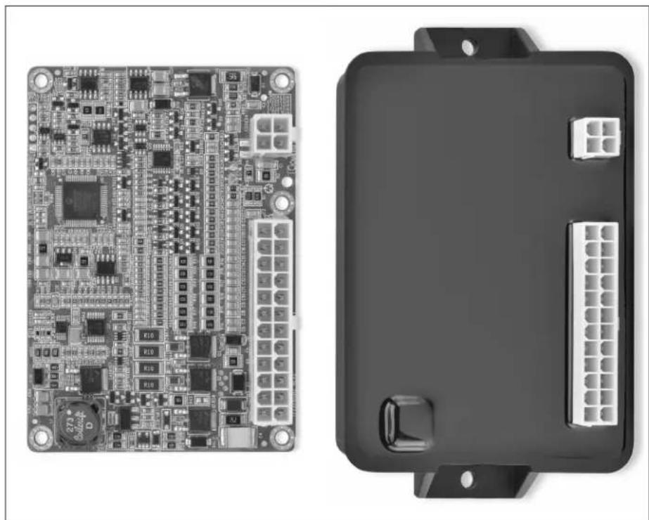
Features include:
√ 11 active-high digital inputs
√ 2 high-frequency driver outputs (1 amp and 3 amps), which can also be used as active-high digital inputs
√ Closed loop constant current, constant voltage, or direct PWM control on each output
√ 5 analog inputs (0–15V), which can also be used as virtual digital inputs with programmable thresholds
More Features
√ Analog inputs are selectable for resistive sensors (0–5 kΩ)
√ 1 quadrature encoder input
√ Serial port for Curtis programmer or fault code display
√ CANopen communication port controlled by dynamic mapping
√ Regulated 5V and unregulated 12V current-limited power supplies
√ The output voltage and current of the 5V and 12V supplies can be monitored
√ Software and hardware watchdog circuits ensure proper software operation
√ IP65-rated protection for 1356P (exclusive of connectors)
√ Red and yellow status LEDs provide external monitoring.
DESCRIPTIONS OF KEY FEATURES
Active-High Digital Inputs
The 1356 /1356P has eleven digital inputs. Each input is digitally filtered to eliminate switch “bounce” or noise in the signal. A power resistor pull-down to B- at each input provides active high to B+.
High Frequency Driver Outputs
The 1356 /1356P contains two driver outputs. One can sink up to 1 amp through an inductive or a resistive load; the other can sink up to 3 amps through an inductive or a resistive load. Internal flyback diodes to B+ prevent voltage spikes. High frequency PWM (16 kHz) provides smooth current to the load.
Constant Current or Voltage Outputs
The two driver outputs can work in Constant Current mode or in Constant Voltage mode.
In Constant Current mode, the software runs a closed loop PI controller to provide an average constant current. This current is commanded over PDO as a 0–100% command based on the maximum current setting (set through a Curtis programmer or an SDO).
Each output can also be programmed for Constant Voltage mode. In this mode, the battery voltage is monitored and the PWM command is corrected by a feed-forward controller to provide a constant average voltage commanded over the PDO (a 0–100% command based on the maximum voltage setting).
In addition, each output can also be programmed to provide a directly commanded PWM% output (Direct PWM mode) or shut off to be used as an input (Active-High Digital Input Only mode).
Programmable Dither for Hydraulic Valves
Dither is a small variation in the command that keeps the seals of a proportional valve oiled. This lubrication allows the valve to move freely for accurate PV control. Dither is only active on drivers in Constant Current mode.
Voltage Analog Inputs
The 1356 /1356P has five analog inputs that are scaled to read 0 - 15 volts. The analog channels are read by a 12-bit ADC, resulting in about 3.66 millivolt resolution. Independently adjustable filters ensure a smooth signal.
Resistive Sensor Inputs
Each analog input can be used with resistive sensors, such as RTDs (Resistive Temperature Devices).
Virtual Digital Inputs
The five analog inputs are also sensed and decoded as if they were digital inputs. A unique feature of these digital inputs is that the active high/low thresholds are completely programmable. Thus, these inputs can be used with analog sensors to detect conditions like over/under pressure, high/low level points, etc.
Encoder Interface
The 1356 /1356P has one quadrature encoder input, which shares with the Analog 4–5 pins. The 1356 /1356P can detect an open fault on the encoder input wire.
CAN Interface
The 1356 /1356P is CANopen compliant, responding to the standard NMT, PDO, and SDO communications as well as the DS301-required identity and standard objects. The Curtis CANopen extensions allow additional features, such as OEM and User default configurations and time-stamped fault logging.
PDO Dynamic Mapping
The 1356 /1356P can receive two PDOs and respond with two PDOs. These PDOs use dynamic mapping. All programmable parameters and viewable values within the 1356 /1356P are accessible by SDOs or with a Curtis programmer.
Online Update
The 1356 /1356P has the ability to update its software through the serial port (with Curtis 1309USB) or through the CANopen interface (with Peak-CAN tools), using existing Curtis PC software tools.
Status LEDs
The 1356 has two fault LEDs (red and yellow) to clearly flash the fault code. Both the 1356 and the 1356P can drive a single remote LED via the serial port, to flash the fault code.
Familiarity with your Curtis 1356/1356P module will help you install and operate it properly. We encourage you to read this manual carefully. If you have questions, please contact the Curtis office nearest you.
2

Fig. 2 Mounting dimensions, Curtis 1356 and 1356P expansion modules.
INSTALLATION AND WIRING
MOUNTING THE MODULE
The outline and mounting hole dimensions for the modules are shown in Fig. 2.
The 1356P module should be mounted using two M4 screws.
The 1356 module requires the OEM to develop an appropriate case to provide environmental protection. Mounting for the 1356 depends on the case.
Care should be taken to prevent contaminating the PCBA (1356) or connector (1356P). In order to prevent external corrosion and leakage paths from developing, the mounting location should be carefully chosen to keep the module as clean and dry as possible.


Dimensions in millimeters.

If the outputs will be used at or near their maximum ratings, it is recommended that the module be mounted to a good heatsinking surface, such as an aluminum plate.
You will need to take steps during the design and development of your end product to ensure that its EMC performance complies with applicable regulations; suggestions are presented in Appendix A.
The 1356/1356P contains ESD-sensitive components. Use appropriate precautions in connecting, disconnecting, and handling the module. See installation suggestions in Appendix A for protecting the module from ESD damage.
CAUTION
Working on electrical systems is potentially dangerous. You should protect yourself against uncontrolled operation, high current arcs, and outgassing from lead acid batteries:
UNCONTROLLED OPERATION — Some conditions could cause the motor to run out of control. Disconnect the motor or jack up the vehicle and get the drive wheels off the ground before attempting any work on the motor control circuitry.
HIGH CURRENT ARCS — Batteries can supply very high power, and arcing can occur if they are short circuited. Always open the battery circuit before working on the motor control circuit. Wear safety glasses, and use properly insulated tools to prevent shorts.
LEAD ACID BATTERIES — Charging or discharging generates hydrogen gas, which can build up in and around the batteries. Follow the battery manufacturer's safety recommendations. Wear safety glasses.
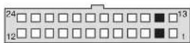
CONNECTIONS
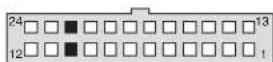
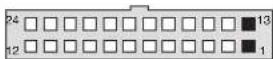
The 1356/1356P connections are made through 24-pin and 4-pin Molex connectors. The mating plugs are Molex #39-01-2245 and #39-01-2045, and the contact pins are #39-00-0059.
The individual pins are characterized in Tables 1 and 2.

J1

J2
Table 1 24-Pin Molex Connector Pin Assignment
| PIN NAME DESCRIPTION | PIN | NAME | DESCRIPTION | ||
| J1-1 B+ Battery positive. | J1-13 | B- | Battery negative. | ||
| Active High Digital Input1 & J1-2 Input/Output 1 High Power PWM Active Low Output1. | Active High Digital Input2 & J1-14 Input/Output 2 Output2. | High Power PWM Active Low | |||
| J1-3 Input 3 Active High Digital Input3. | J1-15 | Input 4 Active High Digital Input4. | |||
| J1-4 Input 5 Active High Digital Input5. | J1-16 | Input 6 Active High Digital Input6. | |||
| J1-5 Input 7 Active High Digital Input7. | J1-17 | Input 8 Active High Digital Input8. | |||
| J1-6 Input 9 Active High Digital Input9. | J1-18 | Input 10 | Active High Digital Input10. | ||
| J1-7 Input 11 Active High Digital Input11. | J1-19 | Input 12 | Active High Digital Input12. | ||
| J1-8 Input 13 Active High Digital Input13. | J1-20 | Analog Input 1 | Voltage or Resistive Input1. | ||
| J1-9 Analog Input 2 Voltage or Resistive Input2. | J1-21 | Analog Input 3 | Voltage or Resistive Input3. | ||
| Voltage or Resistive Input4 & J1-10 Analog Input 4/ Encoder A Quadrature Encoder Input Phase A. | Voltage or Resistive Input5 & J1-22 Analog Input 5/ Encoder B | Quadrature Encoder Input Phase B. | |||
| J1-11 CAN H CAN Communication Line. Bus High | J1-23 CAN L Communication Line. | CAN Bus Low | |||
| J1-12 +5V Regulated Low Power +5V Output. | J1-24 | I/O GND Reference. | Input and Output Ground | ||
| Table 2 4-Pin Molex Connector Pin Assignment | ||
| PIN | NAME | DESCRIPTION |
| J2-1 | Serial Rx/LED Enable | Serial Receive/Status LED Enable. |
| J2-2 | I/O GND | Input and Output Ground Reference. |
| J2-3 | Serial Tx/LED Output | Serial Transmit/Status LED Output. |
| J2-4 | +12V | Unregulated Low Power +12V Output. |
Wiring recommendations
Power (Pins J1-1 and J1-13)
The B+ and B- cables should be run close to each other between the module and the battery. For best noise immunity the cables should not run across the center section of the module. To prevent overheating these pins, the wire gauge must be sufficient to carry the continuous and maximum loads that will be seen at each pin.
Driver outputs (Pins J1-2 and J1-14)
The driver outputs produce high frequency (16 kHz) pulse waves that can radiate RFI noise. The wire from the module to the load should be kept short and routed with the return wire back to the module.
CAN bus (Pins J1-11 and J1-23)
It is recommended that the CAN wires be run as a twisted pair. However, many successful applications at 125 kbit/s are run without twisting, simply using two lines bundled in with the rest of the low current wiring. CAN wiring should be kept away from the high current cables and cross it at right angles when necessary. If the 1356 /1356P is at the end of the CAN bus, the bus needs to be terminated by externally wiring a 120Ω 1/2W resistor across CAN High and CAN Low (for those models that do not have a 120Ω terminal resistor between CAN H and CAN L).
All other low current wiring
The remaining low current wiring should be run according to standard practices. Running low current wiring next to the high current wiring should always be avoided.
WIRING: BASIC CONFIGURATION
A basic wiring diagram is shown in Fig. 3, and described below. The diagram shows the standard power and battery connections, as well as some basic uses for the inputs and outputs.

Fig. 3 Basic wiring diagram, Curtis 1356/1356P CAN expansion module.
Power Connection
The battery is connected to the module's B+ pin though a fuse, a diode, and a keyswitch. The fuse protects the wiring in the event of a short or failure. The return path of the coils is also brought back to the B+ pin to utilize the flyback diodes connected inside the module between B+ and each driver output.
The keyswitch is used to turn on the system. When the keyswitch is closed, B+ goes high and the 1356 /1356P's power supply brings up the module.
Driver Outputs
Each of the two driver outputs (Output 1, 2) is capable of driving a closed-loop current-controlled proportional valve or a voltage-controlled contactor. Each driver has independent mode, max, and dither settings.
These are high-power drivers. The internal impedance to ground will cause leakage current to flow through the output even when the output driver is off. This leakage current can be enough (>2 mA) to light high-efficiency LEDs.
In the wiring diagram, the output at J1-2 is shown driving a proportional valve coil. This driver is programmed for Constant Current mode and would have some Dither applied.
The second output, at J1-12, is driving a basic contactor coil. This output is in the Constant Voltage mode and can be set to run at a lower voltage than the nominal battery voltage.
Switch Inputs
All the inputs are used as Active High inputs (“On” when connected to B+). In the wiring diagram, Input 13 (J1-8) is shown as an Active High input switching to B+.
(Note that when Input/Output 1 or 2 is used as a switch input, its Operation Mode must be set to 0; see pages 33 and 45.)
Analog Inputs
Analog Input 3, at J1-21, is shown being used with an RTD. This requires setting Analog Input 3's Input Type parameter to 1 = Resistive input (see pages 34 and 43).
CAN Bus
The 1356 /1356P has an internal 1kΩ bus termination resistor. This internal impedance matches the system requirements for a mid-line connection or short stub connection. The 1356 /1356P can communicate up to 1 Mbit/s on a properly terminated/wired bus.
WIRING: Application Example
The wiring diagram in Fig. 4 provides an example of a fingertip joystick application for an electric forklift.
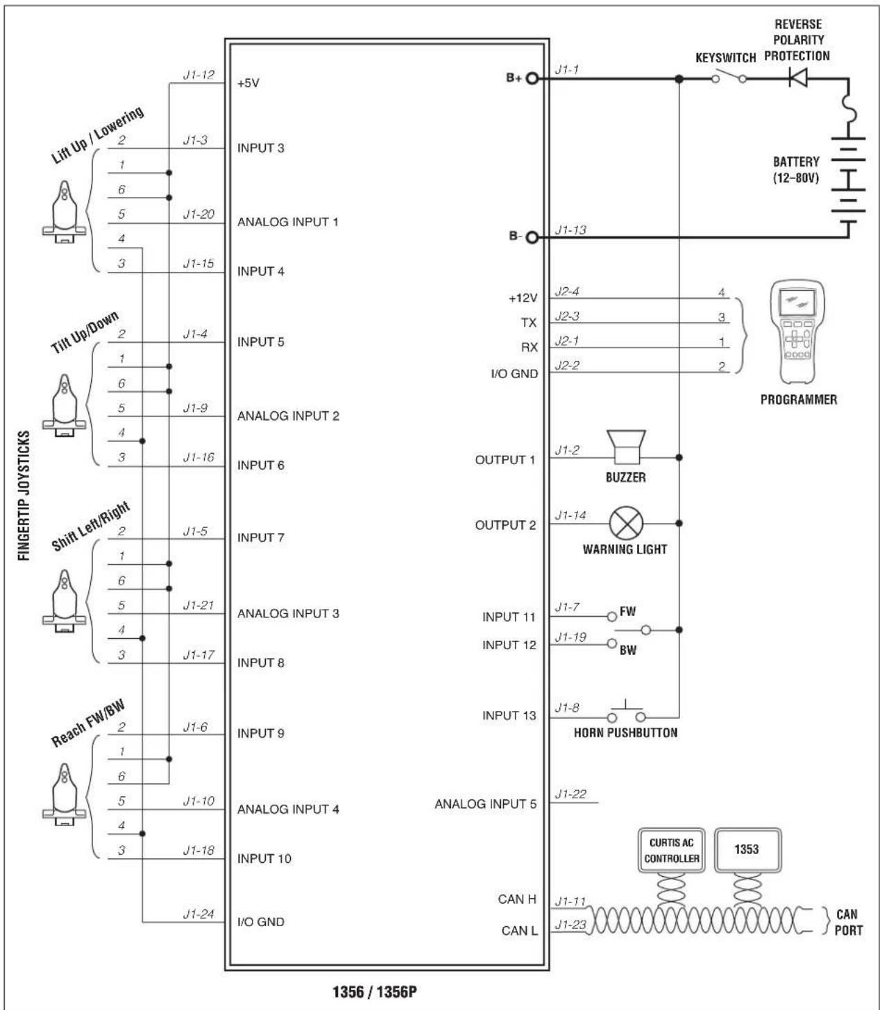
Fig. 4 Application example, Curtis 1356/1356P CAN expansion module.
INPUT/OUTPUT SIGNAL SPECIFICATIONS
The input/output signals wired to the 24-pin connector can be grouped by type as follows; their electrical characteristics are discussed below.
- digital inputs
— driver outputs
— analog inputs with virtual digital input
— encoder inputs
— serial port
— CAN Bus interface
— auxiliary power supplies.

Digital Inputs
The 1356/1356P has eleven digital inputs. In addition, the two driver outputs (Input/Output 1 and Input/Output 2) can be programmed as digital inputs (as long as the drivers are off: i.e., no current, voltage, or PWM output). Each of these digital inputs has a pull-down resistor to B-. This provides an active high input ("On" when connected to B + ). The side effect of this pull-down resistor is that there is a small leakage current in the two driver outputs when the output driver is Off. This leakage can be enough ( >2mA ) to light high-efficiency LEDs.
| DIGITAL INPUT SPECIFICATIONS | |||
| SIGNAL NAME | PIN | LOGIC THRESHOLD | INPUT IMPEDANCE |
| Input/Output 1 J1 | -2 | All models:Low = 1.6 V aboutHigh = 4.0 V | 12–36V models:10 kΩ36–80V models:about 47 kΩ |
| Input/Output 2 J1 | -14 | ||
| Input 3 J1-3 | |||
| Input 4 J1-15 | |||
| Input 5 J1-4 | |||
| Input 6 J1-16 | |||
| Input 7 J1-5 | |||
| Input 8 J1-17 | |||
| Input 9 J1-6 | |||
| Input 10 | J1-18 | ||
| Input 11 | J1-7 | ||
Because Input/Output 1 and Input/Output 2 can also be used as driver outputs, it is important to ensure that Operation Mode is set appropriately. When they will be used as digital inputs, the Operation Mode parameter must be set to 0 = Active High Digital Input (see pages 33 and 45). Otherwise, a direct short from the battery through the internal driver FET will occur when the input is switched high and the FET is turned on.
Driver Outputs
The 1356 /1356P contains two driver outputs. These outputs have all the features necessary to drive proportional valves as well as many other inductive and non-inductive loads. A variable amount of dither (fixed frequency command "jitter") can be added to the PWM to prevent proportional valves from sticking in place.
| DIGITAL OUTPUT SPECIFICATIONS | ||||
| SIGNAL NAME | PIN | MAX CURRENT | IMPEDANCE | FREQUENCY |
| Input/Output 1 J1-23A | 12–36V models: All models:10 kΩ pulldown to B- | 16 kHz0–100% duty cycle | ||
| Input/Output 2 J1-14 | 1A | 36–80V models:47 kΩ pulldown to B- | ||
The drivers can be set for Constant Current, Constant Voltage, or Direct PWM control mode.
In Constant Current mode, the driver command of 0 to 100% is interpreted as a current from 0 to the Max Output setting. Internal current shunts are measured and fed back to a closed loop PI controller to provide a steady current over changing loads and supply voltages.
In Constant Voltage mode, the driver command of 0 to 100% is interpreted as a voltage from 0 to Max Output. The battery voltage is constantly monitored and fed back to a closed loop PI controller to provide a steady voltage, compensating for battery droop and discharge. If the command is higher than the driver can output, the PWM will max out at 100%.
In Direct PWM mode, the driver command of 0 to 100% is directly output on the driver.
Each driver is monitored and will detect a short in the load, a failed internal driver FET, and/or an open in the load wiring. At near 0% and 100% PWM, it is not possible to discern each fault and some faults will not be detected.
If the driver outputs are connected to inductive loads, the coil should have a return line to the B+ pin of the 1356/1356P. This connection provides a path for the internal freewheel diodes to clamp the turn-off spike. Failure to make this connection with inductive loads can cause permanent damage to the 1356/1356P as well as propagate failures of other electronics in the system due to the high voltage spike caused when an inductive load turns off without a freewheel path.

Analog Inputs
The 1356 /1356P has five 0 – 15 V analog inputs. These inputs are scaled down by 5.76, clamped to 3.3 V, and read by a 12-bit ADC internal to the MCU.
| ANALOG INPUT SPECIFICATIONS | ||||
| SIGNAL NAME | PIN | VOLTAGE | VOLTAGEINPUT IMPEDANCE RANGE | PROTECTED |
| Analog Input 1 J1-20 | Nominal input voltage:0–15VInput maximumreverse voltage: -1.7V | Voltage Input Type:about 21 kΩResistance Input Type:about 1 kΩ | -1 V to B+ | |
| Analog Input 2 J1-9 | ||||
| Analog Input 3 J1-21 | ||||
| Analog Input 4 J1-10 | ||||
| Analog Input 5 J1-22 | ||||
The maximum resistive input on each analog input is 7.5 kΩ. The resistive or voltage type of analog input can be selected by a Curtis programmer (1313/1314) or CAN SDO message.
These five analog inputs can also be used as digital inputs. A unique feature of these digital inputs is that the active high/low thresholds are completely programmable. Thus, these inputs can be used with analog sensors to detect conditions like over/under pressure, high/low level points, etc.
Encoder Inputs
Analog Inputs 4 and 5 can be configured as a quadrature encoder input (Encoder A and B). This standard quadrature encoder input accepts open collector encoders with pull-up resistors in the 1356/1356P module. The encoder can be powered from the +5V supply (J1-12) or the +12V supply (J2-4) while using the I/O GND (J1-24) as a common.
| ENCODER INPUT SPECIFICATIONS | ||||||
| ENCODER PHASE | PIN | Vth LO | Vth HI | FREQUENCY MAX | INPUT IIMPEDANCE | PROTECTED VOLTAGE RANGE |
| A | J1-10 | 1.0V | 2.2V | 15kHz | 1kΩ (internal pull-up to +4.4V) | -1V to B+ |
| B | J1-22 | |||||

Serial Port
The Curtis 1313/1314 programmer or the Curtis Model 840 can be connected to the 1356 /1356P's serial port, J2.
| SERIAL PORT SPECIFICATIONS | ||||
| PROTECTEDVOLTAGESIGNAL NAME PIN | PROTOCOL / DEVICES | DATA RATE | RANGE | |
| TX | J2-3 | 1313 Handheld Programmer,1314 PC Programming Station,Curtis 840 Display | As required,9.6 to 56 kbit/s | -0.3 V to 12 V |
| RX | ||||
Power is provided through J2-4 (+12V) and J2-2 provides the I/O ground reference.
When the 840 is connected to the serial port, it will alternately show BDI, hour meter, and fault information.
The serial port can also be used as an external Status LED fault code display. When the serial port is used for fault code display, a jumper must be added between J2-1 and J2-4, and an LED is connected between J2-2 and J2-3.
![graph TD A["Diode 1"] --> B["Component 2"] A --> C["Component 4"] A --> D["Component 1"] A --> E["Component 3"]](/content/2026/07/1422497/images/351feb67c3111e87db90abec17ea1c561d3de3ebba6d0f62ab8f9c450b8d9c7f.jpg)

CAN Bus Interface
The CAN bus interface will comply with CAN2.0B, active from 50 kbit/s to 1 Mbit/s communication rate.
The 1356/1356P will be terminated by an internal 1 kΩ resistor across the CAN High and Low communication pins. This assumes a mid-truck connection (not end-of-line).
If a 1356/1356P without terminal resistance (models ending in -4101 or -6101) is at the end of the CAN bus, the bus needs to be terminated by externally wiring a 120 Ω, ½W resistor across CAN High and CAN Low.

Auxiliary Power Supplies
The 1356/1356P provides +12V and +5V auxiliary output power for low power circuits such as fingertip joysticks, electronic throttle, Curtis programmer, Curtis 840 display, or remote I/O boards. The return line for these low power circuits is I/O GND. The maximum total combined output current is 200 mA.
| AUXILIARY POWER SUPPLY SPECIFICATIONS | |||||
| SIGNAL NAME | PIN | VOUT | VOUT TOLERANCE | IOUT (MAX) | RIPPLE/NOISE |
| +12V | J2-4 | 12V | 10 % | 100 mA | 2 % |
| +5V | J1-12 | 5V | 5 % | 100 mA | 2 % |
Power
The power pins are each capable of carrying up to 9 A. Every application must use B+ (J1-1) and B- (J1-13).
3
CANopen COMMUNICATIONS
The 1356 /1356P adheres to the industry standard CANopen communication protocol and thus will easily connect into many CAN systems, including those using the Curtis AC and Vehicle System controllers. Any CANopen-compatible master can be programmed to control the 1356 /1356P.
The 1356/1356P receives two incoming (MOSI) PDOs and responds with two outgoing (MISO) PDOs. Dynamic mapping is available for the PDOs. All programmable parameters and monitor parameters are accessible by standard SDO transfer.
The time between incoming PDOs is monitored and if excessive, will flag a fault. This allows the 1356 /1356P to know that the system is still under master control. The 1356 /1356P also produces Heartbeat and Error messages, which is the CiA-preferred safety and security method.
MINIMUM STATE MACHINE
The 1356 /1356P will run the CANopen minimum state machine as defined by CiA. The CANopen minimum state machine has four defined states: Initialization, Pre-Operational, Operational, and Stopped.
![graph TD A["Power-On Reset"] --> B["Initialization"] B -->|Transmit Boot-up| C["Pre-Operational"] C --> D["Operational"] D --> E["Stopped"] E --> F["Reset Module"] F --> A C --> G["Reset Communication"] G --> F B --> H["Reset Module"] H --> F C --> I["Stopped"] I --> E](/content/2026/07/1422497/images/9004975923652e9200881afc9f9a3cd73cb5d214e5a3521b7bca4e987b2f11bb.jpg)
When the 1356/1356P powers up, it goes to the Initialization state; this is also known as the Boot-up state. No CAN communications from the 1356/1356P are transmitted in this state although the 1356/1356P listens to the CAN bus. When the 1356/1356P has completed its startup and self-tests, it issues an initialization heartbeat message and automatically goes to the Pre-Operational state.
In the Pre-Operational state, the 1356 /1356P can receive and respond to SDOs and NMT commands, and will send its heartbeat. It will not receive or send PDOs (unless PDO-MISO cyclic transmitting is enabled). After receiving an Operational State NMT command, the 1356 /1356P will enter the Operational state (full normal operation).
In the Operational state, the 1356/1356P will start receiving and responding to PDOs and process all other necessary CANopen messages.
Baud Rates
The 1356 /1356P runs at one of the seven selectable baud rates: 50 kbit/s, 100 kbit/s, 125 kbit/s, 250 kbit/s, 500 kbit/s, 800 kbit/s, or 1 Mbit/s. The baud rate can be changed by a Curtis programmer or by an SDO. Changes in the baud rate require an NMT reset or KSI cycle.
CAN Node ID
The 1356/1356P CAN node ID can be assigned from 1 to 127. It can be changed by a Curtis programmer or by CAN SDO. The default CAN node ID for the 1356/1356P is 19. The CAN node ID is used by CANopen to route messages to the 1356/1356P and to denote messages from the 1356/1356P. The node ID is part of the COB-ID and therefore also plays a part in message priority and bus arbitration. Changes to the node ID require an NMT reset or KSI cycle.
Standard Message Identifiers
The standard message types are defined within a 4-bit field in the COB ID (Communication OBject IDentification). Consequently, there are 16 possible standard message types. The values for Curtis products are:
| Generic Type Message Identifier Value (binary - hex) | ||
| NMT NMT 0000 - 0x0 | ||
| EMERGENCY SYNC_ERR 0001 - 0x1 | ||
| PDO PDO1_MISO 0011 - 0x3 | ||
| PDO1_MOSI 0100 - 0x4 | ||
| PDO2_MISO 0101 - 0x5 | ||
| PDO2_MOSI 0110 - 0x6 | ||
| SDO SDO-MISO | 1011 - 0xB | |
| SDO_MOSI 1100 - 0xC | ||
| HEARTBEAT | NODE | 1110 - 0xE |
These types and values comply with the CANopen spec and are used to invoke standard transfer or information across the CAN bus.
Identifiers built using standard message types consist of three fields. The four upper bits hold the message type. The Node ID is in the bottom 7 bits.
Below is the CANopen-compliant Curtis standard organization of the COB-ID.

NMT messages have the highest priority of the standard message types, and the heartbeat has the lowest priority.
NMT MESSAGES
NMT (Network Management Transmission) messages are the highest priority message available. The NMT message puts the 1356 /1356P into a specific Device State, as shown below. These messages have 2 bytes of data sent by the master; the slave does not respond with any data to an NMT.
The Device State value can be queried over the CAN bus using an SDO. The Device State value is also transmitted with each heartbeat message.
| Value | Device State |
| 0 | Initialization (or “boot-up”) |
| 4 | Stopped |
| 5 | Operational |
| 127 | Pre-Operational |
The NMT message identifier consists of the standard message type, NMT, in the top four bits. The bottom seven bits must be set to zero.
The first data byte of the NMT command is the command specifier. The 1356 /1356P will respond to the following commands.
| Value | Command Specifier |
| 0x01 | Enter the Operational state |
| 0x02 | Enter the Stopped state |
| 0x80 | Enter the Pre-Operational state |
| 0x81 | Reset the 1356 /1356P (warm boot) |
| 0x82 | Reset the CAN bus |
The second byte of the NMT command defines whether this NMT is for all slaves on the bus (data byte = 0x00) or for a specific node (data byte = Node ID of the 1356 /1356P).
EMERGENCY MESSAGES
Emergency messages are the second highest priority in CANopen and the highest priority that a slave (like the 1356 /1356P) can transmit. To minimize the number of times Emergency messages can be set, a minimum time between messages can be programmed using a Curtis programmer or an SDO.
Data bytes 1 and 2 define the error category.
Data byte 3 is the CANopen-required error register. Curtis products define this as 0x01 if there is a fault present and 0x00 when all faults are clear.
Data bytes 4 through 8 define the specific fault. The 1356 /1356P will place the current 24-bit hour meter into data bytes 4 through 6.
Bytes 7 and 8 are not used by the 1356 /1356P and are always 0x0000.
The emergency message format indicating an error is shown below.
| byte 1 byte 8 | ||||||
| Curtis Code | 0xFF | 0x01 | 6-bit field | 0x00 | ||
| ← Error Code Hour Meter; ← →: | ||||||
HEARTBEAT
The Heartbeat message is a very low priority message, periodically sent by each slave device on the bus. The Heartbeat message requires no response. Once the 1356 /1356P is in the Pre-Operational state, the Heartbeat message will be issued continually until communication is stopped.
The Heartbeat message has only one data byte. The top bit is reserved and should be set to zero. The bottom 7 bits hold the current NMT device state.
4
PDO COMMUNICATIONS
The PDO (Process Data Object) communication packets conserve bus bandwidth by bundling the values of a group of objects into a single message. The 1356/1356P is controlled and monitored through four PDOs. PDO messages have a medium priority and each PDO always carries 8 bytes of data. The content of these PDOs can be dynamic mapped as Curtis AC motor controllers. For PDO dynamic mapping information, please refer to Curtis document Generic CANopen Implementation.
A PDO transfers 8 bytes of data across the CAN bus. Any given byte is mapped to a single byte of a pre-defined CAN Object. Mapping can be done statically as part of the system design, or it can be done “dynamically” by using SDO transfers. Dynamic mapping is implemented on the 1356/1356P, as described in Section 5: SDO Communications.
PDO-MISO messages can be transmitted either in Cyclic Transmission mode or in standard Master/Slave mode.
The Cyclic Transmission mode allows the 1356 /1356P to periodically transmit the PDO-MOSI at the programmed cycle rate. The cycle rates are adjustable via two parameters: TPDO1 Cycle Rate (for PDO1-MISO) and TPDO2 Cycle Rate (for PDO2-MISO). If the rate is set to 0, the Cyclic Transmission mode will be disabled and only the standard Master/Slave mode will be available.
In standard Master/Slave mode, the 1356/1356P requires the PDO-MOSI to be cyclic from the master. The cycle time must be less than the programmed PDO Timeout. If the PDO-MOSI is not received within the programmed time, the 1356/1356P will flag a PDO Timeout fault and disable all output drivers. If the PDO Timeout parameter is set to 0, the PDO Timeout fault is disabled and the 1356/1356P will respond to any PDO incoming at any rate without faulting.
The following tables describe the PDOs exchanged with default mapping.
PDO1-MOSI (received from the system master)
| Byte 1 Byte 2 Byte 3 Byte 4 Byte 5 | Byte 6 Byte | 7 Byte 8 | |||||
| Output 1 Command | Output 2 Command | BDI (0-100%) | [Reserved] | [Reserved] | [Reserved] | [Reserved] | [Reserved] |
PDO2-MOSI (received from the system master)
| Byte 1 Byte 2 Byte 3 Byte 4 Byte 5 | Byte 6 Byte 7 Byte 8 | ||||||
| [Reserved] | [Reserved] | [Reserved] | [Reserved] | [Reserved] | [Reserved] | [Reserved] | [Reserved] |
PDO1-MISO (sent in response to the system master)
| Byte 1 | Byte 2 | Byte 3 | Byte 4 | Byte 5 | Byte 6 | Byte 7 | Byte 8 | ||||
| Input1–8Status | Input9–13Status | 5 VirtualInputs | [Reserved](0) | AnalogInput 4VoltageValueLow Byte | AnalogInput 4VoltageValueHigh Byte | AnalogInput 5VoltageValueLow Byte | AnalogInput 5VoltageValueHigh Byte | ||||
PDO2-MISO (sent in response to the system master)
| Byte 1 Byte 2 Byte 3 | Byte 4 Byte 5 | Byte 6 Byte 7 | Byte 8 | ||||
| AnalogInput 1VoltageValueLow Byte | AnalogInput 1VoltageValueHigh Byte | AnalogInput 2VoltageValueLow Byte | AnalogInput 2VoltageValueHigh Byte | AnalogInput 3VoltageValueLow Byte | AnalogInput 3VoltageValueHigh Byte | [Reserved](0) | [Reserved](0) |
Output Command Bytes
The drivers are closed-loop controlled, either for current or voltage. This byte sets the output command as a percent of the programmed output limit value: 0–255 = 0%–100%.
BDI
The BDI value is a percent of the battery state of discharge: 0–100 = 0–100%; this value is gotten from the CAN master.
Inputs 1–13 Status Bytes
The 1356/1356P monitors the thirteen digital inputs. The status of these inputs in default PDO-MISO mapping is as follows.
PDO1-MISO Byte 1
| Bit7 | Bit6 | Bit5 | Bit4 | Bit3 | Bit2 | Bit1 | Bit0 | ||
| Digital Input8 Status | Digital Input7 Status | Digital Input6 Status | Digital Input5 Status | Digital Input4 Status | Digital Input3 Status | Digital Input2 Status | Digital Input1 Status | ||
PDO1-MISO Byte 2
| Bit7 | Bit6 | Bit5 | Bit4 | Bit3 | Bit2 | Bit1 | Bit0 | |
| [Reserved] (0) | DigitalInput13Status | DigitalInput12Status | DigitalInput11Status | DigitalInput10Status | DigitalInput9Status | |||
A status of 1 (bit set) indicates that the input is active (pulled high to B+). The upper three bits of Byte 2 are unused and set to 0.
Virtual Digital Inputs Byte
Each analog inputs also produce a “virtual” digital input response. The status of the virtual digital inputs in default PDO-MISO mapping is as follows.
PDO1-MISO Byte 3
Bit7
| Bit6 | Bit5 | Bit4 | Bit3 | Bit2 | Bit1 | Bit0 | |
| [Reserved] (0) | VirtualInput5Status | VirtualInput4Status | VirtualInput3Status | VirtualInput2Status | VirtualInput1Status | ||
If the input is above the programmed High Threshold, the bit will be set to 1. If the input is below the programmed Low Threshold, it will be set to 0. Otherwise, the bit will retain its previous state.
Analog Input High/Low Bytes
The voltage value of the five analog inputs is default mapped in the PDO-MISOs. Each voltage value requires 2 bytes of the PDO packet.
For each analog input, if Resistive Input Type is enabled and the resistance is mapped in PDO-MISOs, the value will be returned as ohms, up to 7.5 kΩ. The value 0xFFFF is interpreted as infinity (wire open).
Encoder Input Bytes
When the Analog Input pair (Analog Input 4&5) is configured as encoder input, the relative PDO bytes will carry the pulse count, RPM value, or position value of the encoder if they are mapped in PDO-MISOs. The encoder input type can be configured as follows.
Pulse Count type
In this type, PDO will output the number of the encoder pulses accumulated. The value is up to 229 - 1 or down to -229 at which point it will roll back to zero.
RPM type
In this type, PDO will send the RPM value (2 bytes, unit in revolutions per minute).
Position type
In this type, PDO will send the position value (2 bytes, unit in millimeters).
5
SDO COMMUNICATIONS
CANopen uses Service Data Objects (SDOs) to change and view all internal parameters, or “objects.” The SDO is an 8-byte packet that contains the address and sub-address of the parameter in question, whether to read or write the parameter, and the parameter data (if it is a write command). SDOs are sent infrequently and have a low priority on the CAN bus.
SDOs are designed for sporadic and occasional use during normal runtime operation. There are two types of SDOs: expedited and block transfer. The 1356 /1356P does not support large file uploads or downloads (using the block transfer), so all the SDOs used by the 1356 /1356P are expedited SDOs.
The SDOs in the 1356 /1356P are used to set up and parameterize the module. They are also used to retrieve basic module information (such as version or manufacture date), review the fault log, and monitor a few key internal variables (mostly for system debug purposes).
SDO Master Request (SDO-MOSI)
An SDO transfer always starts with a request message from the master. Each SDO request message consists of one control byte, a two-byte CAN Object index, a one-byte CAN Object sub-index, and up to 4 bytes of valid data. This format is CANopen compliant.
SDO-MOSI (received from the system master)
The next two bytes hold the CAN Object index. The LSB of the index appears first, in byte 2, and the MSB appears in byte 3. For example, if the index is 0x3021, byte 2 holds the 0x21 and byte 3 holds the 0x30.
Byte 4 holds the CAN Object sub-index. When there is only one instance of a parameter or value type, this value is 0. If there are several related parameters or values, the sub-index is used.
The last four bytes hold the data to be transferred. In the case of a single-byte transfer, the data is placed into byte 5, with bytes 6 through 8 being undefined (set to 0). In the case of a 16-bit transfer, the lower 8 bits appear in byte 5 and the upper 8 bits appear in byte 6; bytes 7 and 8 are undefined (set to 0). The
case of a 32-bit transfer follows the same strategy, with the least significant byte placed in data byte 5 and the most significant byte placed in data byte 8.
SDO 1356 /1356P Response (SDO-MISO)
An SDO request is always acknowledged with a response message from the 1356 /1356P. The 1356 /1356P can issue two kinds of response messages: a normal response or, in case of an error in the request SDO, an Abort SDO Transfer message.
SDO-MISO (sent by 1356 /1356P in response to the system master)
| Byte 1 Byte 2 Byte 3 Byte 4 Byte 5 Byte 6 Byte 7 Byte 8 | ||||
| Control CAN Object Index or the Sub-index Data: either actual Write values, or the requested Read values, an error code | ||||
The first byte of the response contains an acknowledge code, which depends on the type of transfer that was initially requested.
| Action | Byte 1 Value |
| Read Response | 0x40 |
| Write Acknowledge | 0x60 |
| Abort SDO | 0x80 |
Data bytes 2, 3, and 4 hold the CAN Object index and sub-index of the request SDO.
If the SDO is a read command, bytes 5 through 8 will be filled with the requested values, with the LSB in byte 5 and the next least significant in byte 6 and so forth. All unused bytes are set to 0.
If the SDO is a write command, bytes 5 through 8 will return the actual value written in bytes 5–8. In this way, if the 1356/1356P needs to limit or round-down the SDO write request, the master will know—because the return value will be different than the sent value.
If the SDO-MOSI did not properly read or tried to access a parameter improperly, an Abort SDO Transfer will be sent. Bytes 5 through 8 will be filled with a 32-bit error code.
0 x 0 6 0 2 0 0 0 0 = Object does not exist 0 x 0 6 0 1 0 0 0 2 = Attempt to write to a read only object 0 x 0 6 0 4 0 0 4 1 = Object cannot be mapped.
USING AN SDO TO MAP A PDO
The following SDO format shows how to map an SDO to a PDO.
| Byte 1 Byte | 2 Byte 3 | Byte 4 Byte 5 | Byte 6 Byte | 7 Byte 8 | ||||
| Request WR Index | LSB Index | MSB Index | Sub-LSB Index of Object | Index of Object | Sub-index of Object | Length |
Byte 1 contains the request "Write" action, as described earlier.
Bytes 2 through 4 describe the PDO and the byte within the PDO that is to be mapped. Bytes 2 and 3 hold the index indicating the PDO and Byte 4 holds the sub-index (range 1–8) indicating the PDO byte to be mapped.
Bytes 5 through 8 describe the object to be mapped; in other words; they define the object that has the data that will be transmitted. The object index comes first (least significant byte first), followed by the sub-index, followed by the number of bits to be transferred (must be 8). Note that the sub-index here is used to specify a particular byte within a multi-byte object.
For example, take a 32-bit object. To access the least significant byte of a long word (32 bits), the sub-index should be set to 0. To access the most significant byte of a long word (32 bits), the sub-index should be set to 3.
The SDO commands below show an example of mapping the encoder pulse counts (32 bit, index=0x3190) to PDO1-MISO bytes 1–4.
Map the LSB byte to PDO1-MISO Byte 1
In these SDO commands, bytes 2 and 3 hold the index of PDO1_MISO mapping (0x1A00) and the sub-index in byte 4 shows the byte to be mapped. Bytes 5 and 6 hold the object index (0x3190) and the sub-index in byte 7 shows the byte in the 32-bit object to be mapped.
TYPES OF SDO OBJECTS
Three types of SDO objects are described in the following pages: Communications Profile Objects, Programmable Parameter Objects, and Monitor Parameter Objects.
COMMUNICATION PROFILE OBJECTS
The Communication Profile Objects are shown below in Table 2.
| Table 2 Communication Profile Object Dictionary | |||||
| RANGE NAME | ACCESS | INDEX | SUB-INDEX | CAN VALUE | DESCRIPTION |
| Device Type | RO | 0x1000 | 0x00 | 0x00000000 | Predefined type of CAN module (I/O). |
| Error Register | RO | 0x1001= 1 if there is an error | 0x00 | 0 or 1 | = 0 if there are no errors |
| Manufacturer's Status Register 1 | RO | 0x1002 | 0x00 | 2 bytes | The value of the Status Register.See Table 2a for more details. |
| Fault Log(pre-defined error field) | RW | 0x1003 | 0x00 | 0x10 | Length of this object. Clear fault log by writing 0 into this address. |
| RO | 0x01-0x10Emergency Message. | 4 bytes | Contains an array of 16 fault code and time stamps as reported by the | ||
| Node ID | RW | 0x100B | 0x00 | 0x01-0x7F | Node ID of this 1356/1356P. This Object is not part of the CANopen mandatory dictionary. Must cycle power or send an NMT Reset 1356/1356P or NMT Reset CAN for new ID to take full effect. |
| Store Parameters | RW | 0x1010 | 0x00 | 4 bytes | 1356/1356P supports the mandatory Save All Parameters sub-index. See Table 2b for more details. |
| Restore Default Parameters | RW | 0x1011 | 0x00 | 4 bytes | Controls normal, factory, or backup restore. See Table 2c for more details. |
| Emergency COB ID | RO | 0x1014 | 0x00 | 0x00000080-0x000000FF | 11-bit Identifier of the Emergency Message. Only the lowest 11 bits are valid. All other bits must be 0. |
| Emergency Rate | RW | 0x1015 | 0x00 | 0-1000 ms0-1000in 4ms steps | Sets the minimum time that must elapse before another Emergency Message can be sent by the 1356/1356P. A setting of 0 disables |
| Heartbeat Ratein 4ms steps | RW | 0x1017A setting | 0x00of 0 disables | 0-1000 ms0-1000es the Heartbeat. | Sets the cyclic repetition rate of the Heartbeat Message. |
| Table 2 Communication Profile Object Dictionary, cont'd | |||||
| RANGE NAME | ACCESS | INDEX | SUB-INDEX | CAN VALUE | DESCRIPTION |
| Identity Object | RO | 0x1018 | 0x00 | 0x06 | Length of this structure = 6 sub-indexes. |
| RO | 0x01 | 0x00004349 | Curtis ID as defined by CiA. | ||
| RO | 0x02 | 0x054C10050x054C10060x054C17D50x054C17D6 | Product code:2 upper bytes = 1356/1356P,2 lower bytes = model number,-4101, -4102, -6101, or -6102. | ||
| RO | 0x03 | 4 bytes | Hardware version is in byte 1,Software version is in byte 2,Build number version is in byte 3, .Parameter block version is in byte 4. | ||
| RO | 0x04 | 0 – 999999 | Serial Number up to 999,999. | ||
| RO | 0x05 | 1 – 99366 | Date Code up to 99, Dec 31. | ||
| RO | 0x06 | A – Z0x41–0x5A | ASCII code of the manufacturer's location. | ||
Objects describing the PDO Communications and Mapping Parameters
(Note: Each of these objects has dynamic mapping except Nominal Voltage.)
| PDO1-MOSI Parameters | RO | 0x1400 | 0x00 | N/A | Number of PDO1-MOSI communication parameters. |
| 0x01 | COB-ID of PDO1-MOSI. | ||||
| PDO2-MOSI Parameters | RO | 0x1401 | 0x00 | N/A | Number of PDO2-MOSI communication parameters. |
| 0x01 | COB-ID of PDO2-MOSI. | ||||
| PDO1-MOSI Mapping | RO | 0x1600 | 0x00 | N/A | Number of mapped application objects in PDO1-MOSI. |
| PDO1-MOSI Mapping 1st | RW | 0x1600 | 0x01 | N/A | PDO1-MOSI mapping for the 1st application object to be mapped. Default mapped to Driver1 command. |
| PDO1-MOSI Mapping 2nd | RW | 0x1600 | 0x02 | N/A | PDO1-MOSI mapping for the 2nd application object to be mapped. Default mapped to Driver2 command. |
| PDO1-MOSI Mapping 3rd | RW | 0x1600 | 0x03 | N/A | PDO1-MOSI mapping for the 3rd application object to be mapped. Default mapped to BDI. |
| PDO1-MOSI Mapping 4th | RW | 0x1600 | 0x04 | N/A | PDO1-MOSI mapping for the 4th application object to be mapped. Not mapped in default. |
| PDO1-MOSI Mapping 5th | RW | 0x1600 | 0x05 | N/A | PDO1-MOSI mapping for the 5th application object to be mapped. Not mapped in default. |
| PDO1-MOSI Mapping 6th | RW | 0x1600 | 0x06 | N/A | PDO1-MOSI mapping for the 6th application object to be mapped. Not mapped in default. |
| PDO1-MOSI Mapping 7th | RW | 0x1600 | 0x07 | N/A | PDO1-MOSI mapping for the 7th application object to be mapped. Not mapped in default. |
| PDO1-MOSI Mapping 8th | RW | 0x1600 | 0x08 | N/A | PDO1-MOSI mapping for the 8th application object to be mapped. Not mapped in default. |
| Table 2 Communication Profile Object Dictionary, cont'd | |||||
| NAME | ACCESS | INDEX | SUB-INDEX | RANGE CAN VALUE | DESCRIPTION |
| PDO2-MOSI Mapping objects in P | RO 0x1601 | 0x00 | N/A | Number of mapped application | |
| PDO2-MOSI Mapping 1st | PD O2-MOSI mapping for the 1st RW 0x1601 Not mapped in default. | N/A | application object to be mapped. | ||
| PDO2-MOSI Mapping 2nd | PD O2-MOSI mapping for the 2nd RW 0x1601 Not mapped in default. | N/A | application object to be mapped. | ||
| PDO2-MOSI Mapping 3rd | PD O2-MOSI mapping for the 3rd RW 0x1601 Not mapped in default. | N/A | application object to be mapped. | ||
| PDO2-MOSI Mapping 4th | PD O2-MOSI mapping for the 4th RW 0x1601 Not mapped in default. | N/A | application object to be mapped. | ||
| PDO2-MOSI Mapping 5th | PD O2-MOSI mapping for the 5th RW 0x1601 Not mapped in default. | N/A | application object to be mapped. | ||
| PDO2-MOSI Mapping 6th | PD O2-MOSI mapping for the 6th RW 0x1601 Not mapped in default. | N/A | application object to be mapped. | ||
| PDO2-MOSI Mapping 7th | PD O2-MOSI mapping for the 7th RW 0x1601 Not mapped in default. | N/A | application object to be mapped. | ||
| PDO2-MOSI Mapping 8th | PD O2-MOSI mapping for the 8th RW 0x1601 Not mapped in default. | N/A | application object to be mapped. | ||
| PDO1-MISO Parameters | RO | 0x1800 0x01 | 0x00 | Number of PDO1-MISO communication parameters. | |
| COB-ID | of PDO1-MISO | ||||
| TPDO1 Cycle Rate | RW | 0x1800 | 0x05 | 0-1000 ms 0-1000 | Periodic transmit rate of PDO1-MISO (in 4ms steps). Setting to 0 will disable periodic transmit. |
| PDO2-MISO Parameters | RO | 0x1801 0x01 | 0x00 | Number of PDO2-MISO communication parameters. | |
| COB-ID | of PDO2-MISO | ||||
| TPDO2 Cycle Rate | RW | 0x1801 | 0x05 | 0-1000 ms 0-1000 | Periodic transmit rate of PDO2-MISO (in 4ms steps). Setting to 0 will disable periodic transmit. |
| PDO1-MISO Mapping objects in P | RO 0x1A00 | 0x00 | N/A | Number of mapped application | |
| PDO1-MISO Mapping 1st | RW | 0x1A00 | 0x01 | N/A | PDO1-MISO mapping for the 1st application object to be mapped. Default mapped to LSB byte of |
| PDO1-MISO Mapping 2nd | RW | 0x1A00 | Switch Input States. | N/A | PDO1-MISO mapping for the 2nd application object to be mapped. Default mapped to MSB byte of |
Table 2 Communication Profile Object Dictionary, cont'd
| RANGE NAME | ACCESS | INDEX | SUB-INDEX | CAN VALUE | DESCRIPTION |
| PDO1-MISO Mapping 3rd | RW | 0x1A00 | 0x03 | N/A | PDO1-MISO mapping for the 3rd application object to be mapped. Default mapped to LSB byte of Virtual Digital Input States. |
| PDO1-MISO Mapping 4th | RW | 0x1A00 | 0x04 | N/A | PDO1-MISO mapping for the 4th application object to be mapped. Default mapped to MSB byte of Virtual Digital Input States. |
| PDO1-MISO Mapping 5th | RW | 0x1A00 | 0x05 | N/A | PDO1-MISO mapping for the 5th application object to be mapped. Default mapped to LSB byte of Analog4 Voltage Value. |
| PDO1-MISO Mapping 6th | RW | 0x1A00 | 0x06 | N/A | PDO1-MISO mapping for the 6th application object to be mapped. Default mapped to MSB byte of Analog4 Voltage Value. |
| PDO1-MISO Mapping 7th | RW | 0x1A00 | 0x07 | N/A | PDO1-MISO mapping for the 7th application object to be mapped. Default mapped to LSB byte of Analog5 Voltage Value. |
| PDO1-MISO Mapping 8th | RW | 0x1A00 | 0x08 | N/A | PDO1-MISO mapping for the 8th application object to be mapped. Default mapped to MSB byte of Analog5 Voltage Value. |
| PDO2-MISO Mapping | RO | 0x1A01 | 0x00 | N/A | Number of mapped application objects in PDO2-MISO. |
| PDO2-MISO Mapping 1st | RW | 0x1A01 | 0x01 | N/A | PDO2-MISO mapping for the 1st application object to be mapped Default mapped to LSB byte of Analog1 Voltage Value. |
| PDO2-MISO Mapping 2nd | RW | 0x1A01 | 0x02 | N/A | PDO2-MISO mapping for the 2nd application object to be mapped Default mapped to MSB byte of Analog1 Voltage Value. |
| PDO2-MISO Mapping 3rd | RW | 0x1A01 | 0x03 | N/A | PDO2-MISO mapping for the 3rd application object to be mapped Default mapped to LSB byte of Analog2 Voltage Value. |
| PDO2-MISO Mapping 4th | RW | 0x1A01 | 0x04 | N/A | PDO2-MISO mapping for the 4th application object to be mapped Default mapped to MSB byte of Analog2 Voltage Value. |
| PDO2-MISO Mapping 5th | RW | 0x1A01 | 0x05 | N/A | PDO2-MISO mapping for the 5th application object to be mapped Default mapped to LSB byte of Analog3 Voltage Value. |
| PDO2-MISO Mapping 6th | RW | 0x1A01 | 0x06 | N/A | PDO2-MISO mapping for the 6th application object to be mapped Default mapped to MSB byte of Analog3 Voltage Value. |
| Table 2 Communication Profile Object Dictionary, cont'd | |||||
| RANGE NAME | ACCESS | INDEX | SUB-INDEX | CAN VALUE | DESCRIPTION |
| PDO2-MISO Mapping 7th | RW | 0x1A01 | 0x07 | N/A | PDO2-MISO mapping for the 7th application object to be mapped Not mapped in default. |
| PDO2-MISO Mapping 8th | RW | 0x1A01 | 0x08 | N/A | PDO2-MISO mapping for the 8th application object to be mapped Not mapped in default. |
Table 2 Column Definitions
Access: RO = Read Only access; RW = Read/Write access
Index: The CAN address that is used to access this object.
Sub-index: Some objects have several values associated with them.
In these cases, a Sub-index is used to access each part of the object.
Detail on the Manufacturer's Status Register, Store Parameters, and Restore Parameters objects is presented in Tables 2a, 2b, and 2c.
Manufacturer's Status Register
The Manufacturer's Status Register reflects the present fault flags. Each fault has its own bit in the Status Register. Unlike the LED Status of the Emergency Message, which can only relay the highest priority fault, the 16-bit Status Register will show all present faults. See Section 6: Diagnostics and Troubleshooting for descriptions and probable causes of the faults.
| Table 2a Manufacturer's Status Register | |
| BIT LOCATION | FAULT |
| LSB: Bit 0 | Internal Fault |
| Bit 1 | Flash Fault |
| Bit 2 | 5V Supply Fail |
| Bit 3 | 12V Supply Fail |
| Bit 4 | External Supply Out of Range |
| Bit 5 | EEPROM Fault |
| Bit 6 | Encoder Fault |
| Bit 7 | Analog Input Fault |
| Bit 8 | Overvoltage |
| Bit 9 | Undervoltage |
| Bit 10 | Driver 1 Fault |
| Bit 11 | Driver 2 Fault |
| Bit 12 | Coil 2 Fault |
| Bit 13 | Coil 2 Fault |
| Bit 14 | PDO Timeout |
| Bit 15 | CAN Bus Fault |
Store Parameter Object
The 1356 /1356P has three parameter blocks: the Normal parameter block, Back-up parameter block, and Factory parameter block. An SDO or 1313/1314 programmer Write operation will update the parameter in working RAM. All parameters in working RAM will be saved to the Normal parameter block after KSI cycle.
The text string “bkup” initiates a complete storage of all parameters to the Backup parameter block.
| Table 2b Store Parameter Object | |||
| Function Request Value Access Description | |||
| BACK_UP_COMMAND | “bkup”0x70756B62 | WO | Text string that commands all parameters to be saved from working RAM to the Backup flash space. |
At first glance, the ASCII looks “backward.” This is because CANopen defines that the LSB goes first and MSB is sent last. Therefore “bkup” (which is data bytes 5, 6, 7, and 8) is written as “pukb” when converting it to hex (data
bytes in proper descending order). Using the ASCII hex values for each character, we get 0x70 ("p"), 0x75 ("u"), 0x6B ("k"), and 0x62 ("b") for the final resultant hex 4 byte number of 0x70756B62.
Restore Default Parameters
The Restore Default Parameters Object allows the 1356 /1356P to restore all flash backed-up SDO objects to their Factory settings (hard-coded in software), Back-up settings (stored in Back-up parameter block in flash), or Normal (stored in Normal parameter block in flash). This object can also be used to restore (reset) the hour meter value.
Writing a special text string to this object will initiate a restore to Factory, Backup, or Normal settings for all SDO objects stored in flash. Once this object is written to, the next KSI cycle will cause the system settings to be loaded from the new desired location and put into the working RAM locations (Shadow RAM).
A Restore the Back-Up Settings command ("load") will load the data values from the Backup parameter block, place them in RAM, and overwrite the Normal parameter block with them. Whatever changes were made to the Normal parameter block will be lost. The Restore Default Parameters function should be set to 0x02 (Restore Normal Settings) so that the 1356 /1356P will restore from the Normal parameter block on the next reset or power cycle.
| Table 2c Restore Default Parameters Object | |||
| Restore Default Write DataParameters Function String Read Back Description | |||
| Restore Factory Settings | “fact”0x74636166 | 0 | Restore all parameter values from built-in defaults. These are hard-coded in the software. |
| Restore the Back-Up Settings | “load”0x64616F6C | 1 | Restore all parameter values from the Backup parameter block. “load” is used to comply with CANopen spec DS301. |
| Restore Normal Settings | “norm”0x6D726F6E | 2 | Restore all parameter values from the Normal parameter block. |
| Preset the Hour Meter | “hour”0x72756F68 | N/A | Preset the hour meter to the value loaded into the parameter Preset Hour (0x3062). |
On reception of the correct string, the 1356 /1356P will set a Restore flag and confirm the SDO transmission. If a wrong string or unsupported command is written, the 1356 /1356P will not set the Restore flag and responds with an Abort SDO.
The hour meter has a special function to reset it. Writing the string “hour” to this index will cause the 1356 /1356P to preset the hour meter to the value saved in the Preset Hour parameter (0x3062). Note that only the hours can be set to a programmed value; the minutes always will be reset to 0.
PARAMETER PROFILE OBJECTS
The Programmable Parameter Profile objects are shown in Table 3. All these parameters, except for Nominal Voltage, have dynamic mapping.
| Table 3 Parameter Profile Object Dictionary | ||||
| PARAMETER | SDO LOCATION | RANGE CAN VALUE | DESCRIPTION | |
| INDEX | SUB-INDEX | |||
| Driver1 Mode 0x3000 0x00 0-3, 5-7 | Driver mode: | 0-3, 5-7 | 0 = Active High Digital Input mode.1 = Constant Current mode.2 = Constant Voltage mode.3 = Direct PWM mode.5 = Constant Current mode, with open detection.6 = Constant Voltage mode, with open detection.7 = Direct PWM mode, with open detection. | |
| Driver2 Mode | 0x3001 | 0x00 | See above. | See above. |
| Driver1 Current Limit | 0x3002 | 0x00 | 0.00-3.00 A0-300 | Sets the maximum current output when the PDO command is 100% (255),when operating in Constant Current mode. |
| Driver2 Current Limit | 0x3003 | 0x00 | See above. | See above. |
| Driver1 PWM Limit | 0x3004 | 0x00 | 0-100.0 %0-1000 | Sets the maximum PWM output when the PDO command is 100% (255),when operating in Direct PWM mode. |
| Driver2 PWM Limit | 0x3005 | 0x00 | See above. | See above. |
| Driver1 Voltage Limit | 0x3006 | 0x00 | 0.0-36.0 V0-360(36V models)0.0-80.0 V0-800(80V models) | Sets the maximum voltage output when the PDO command is 100% (255),when operating in Constant Voltage mode. |
| Driver2 Voltage Limit | 0x3007 | 0x00 | See above. | See above. |
| Driver1 Dither Period | 0x3008 | 0x00 | 4-200 ms4-200 | Sets the time between dither pulses for each output (in 2ms steps). A dither period of 4-200 ms provides a frequency range of 250-5Hz.Applicable only in Constant Current mode. |
| Driver2 Dither Period | 0x3009 | 0x00 | See above. | See above. |
| Driver1 Dither Amount | 0x300A | 0x00 | 0-500 mA0-500 | Sets the amount (+/-) of dither that will be added/subtracted from the command (in 10mA steps). Applicable only in Constant Current mode. |
| Driver2 Dither Amount | 0x300B | 0x00 | See above. | See above. |
| Driver1 Kp | 0x300C | 0x00 | 0.1-100.0 %1-1000 | Sets the proportional gain factor of the PI current controller. |
| Driver2 Kp | 0x300D | 0x00 | See above. | See above. |
| Driver1 Ki | 0x300E | 0x00 | 0.1-100.0 %1-1000 | Sets the integral gain factor of the PI current controller. |
| Driver2 Ki | 0x300F | 0x00 | See above. | See above. |
| Nominal Voltage | 0x3010 | 0x00 | 12.0V-36.0V120-360 in36.0V-80.0V360-800 | Sets the nominal battery voltage, which is used fault detection.1356/1356P-4101&-4102: 12V, 24V, 36V.1356/1356P-6101&-6102: 36V, 48V, 60V, 72V, 80V. |
| Table 3 Parameter Profile Object Dictionary, cont'd | ||||
| PARAMETER | SDO LOCATION | RANGE CAN VALUE | DESCRIPTION | |
| INDEX | SUB-INDEX | |||
| Analog Input Type 0x3011 0x00 0 | -31 Sets the | input type on Analog 1 through 5. LSB is for Analog 1 and next is for Analog 2, etc. Upper three bits are not used. Bit = 0, voltage input type. Bit = 1, resistive input type. | ||
| Analog1 High Threshold | 0x3020 | 0x00 | 0.0–15.0 V 0–150 | Sets the threshold that the analog input must go above to set the virtual digital input high. |
| Analog2 High Threshold | 0x3021 | 0x00 | See above. | See above. |
| Analog3 High Threshold | 0x3022 | 0x00 | See above. | See above. |
| Analog4 High Threshold | 0x3023 | 0x00 | See above. | See above. |
| Analog5 High Threshold | 0x3024 | 0x00 | See above. | See above. |
| Analog1 Low Threshold | 0x3030 | 0x00 | 0.0–15.0 V 0–150 | Sets the threshold that the analog input must go below to set the virtual digital input low. |
| Analog2 Low Threshold | 0x3031 | 0x00 | See above. | See above. |
| Analog3 Low Threshold | 0x3032 | 0x00 | See above. | See above. |
| Analog4 Low Threshold | 0x3033 | 0x00 | See above. | See above. |
| Analog5 Low Threshold | 0x3034 | 0x00 | See above. | See above. |
| Analog1 Filter Gain | 0x3040 | 0x00 | 128 s – 8 ms 1–16384 | Sets the amount of filtering on the analog inputs. Higher gains provide faster filtering. Filtering affects the analog reading and the virtual digital input responsiveness. |
| Analog2 Filter Gain | 0x3041 | 0x00 | See above. | See above. |
| Analog3 Filter Gain | 0x3042 | 0x00 | See above. | See above. |
| Analog4 Filter Gain | 0x3043 | 0x00 | See above. | See above. |
| Analog5 Filter Gain | 0x3044 | 0x00 | See above. | See above. |
| Digital1 Debounce Time | 0x3050 | 0x00 | 8–1000 ms 8–1000 | Sets the debounce time of the digital inputs in milliseconds (in 8ms steps) |
| Digital2 Debounce Time | 0x3051 | 0x00 | See above. | See above. |
| Digital3 Debounce Time | 0x3052 | 0x00 | See above. | See above. |
| Digital4 Debounce Time | 0x3053 | 0x00 | See above. | See above. |
| Digital5 Debounce Time | 0x3054 | 0x00 | See above. | See above. |
| Digital6 Debounce Time | 0x3055 | 0x00 | See above. | See above. |
| Digital7 Debounce Time | 0x3056 | 0x00 | See above. | See above. |
| Digital8 Debounce Time | 0x3057 | 0x00 | See above. | See above. |
| Digital9 Debounce Time | 0x3058 | 0x00 | See above. | See above. |
| Digital10 Debounce Time | 0x3059 | 0x00 | See above. | See above. |
| Digital11 Debounce Time | 0x305A | 0x00 | See above. | See above. |
| Digital12 Debounce Time | 0x305B | 0x00 | See above. | See above. |
| Digital13 Debounce Time | 0x305C | 0x00 | See above. | See above. |
| CAN Baud Rate 0x3060 | 0x00 -2 -4 Sets the CAN baud rate:-2-4 | -2 = 50kbit/s.-1 = 100kbit/s.0 = 125kbit/s.1 = 250kbit/s.2 = 500kbit/s.3 = 800kbit/s.4 = 1Mbit/s.Resets to 125 kbit/s when over-range. Must cycle KSI for new rate to take effect. | ||
| PDO Timeout | 0x3061 | 0x00 | 0-1000 ms0-1000 | Sets the time interval (in 4ms steps) within which the PDO MOSI must be received or a fault will be flagged.A setting of zero disables the PDO timeout fault. |
| Preset Hour Meter | 0x3062 | 0x00 | 0-65535 h0-65535 | Writing to this location will change the hours of hour meter and reset the minutes to 0. |
| Encoder Type | 0x3070 | 0x00 | 0-30-3 | Encoder type:0 = Encoder disabled.1 = Pulse count type.2 = RPM type.3 = Position type.Must cycle KSI for new setting to take effect. |
| Encoder Direction | 0x3071 | 0x00 | 0, 10, 1 | Sets the positive direction:0 = Positive direction when phase A is ahead of phase B.1 = Positive direction when phase B is ahead of phase A. |
| Pulses Per Meter | 0x3072 | 0x00 | 0-655350-65535 | This parameter should be set according to the pulses per revolution and displacement per revolution of the encoder.Pulses Per Meter = pulses per revolution/displacement per revolution (unit m) |
| Pulse Per Revolution | 0x3073 | 0x00 | 0-655350-65535 | This parameter should be set according to the encoder specification.Must cycle KSI for new setting to take effect. |
| Encoder Reset | 0x3088 | 0x00 | 0, 10, 1 | Writing 1 to this index will immediately set the encoder counter to zero. |
| Driver1 Command | 0x3090 | 0x00 | 0-2550-255 | Driver output command 0-255 = 0%-100% of max output limit in applicable mode.This command is valid only when mapped and implemented by PDO-MOSI. |
| Driver2 Command | 0x3091 | 0x00 | See above. | See above. |
| BDI | 0x3201 | 0x00 | 0-1000-100 | Displays BDI value (received from the master) on the model 840. |
Driver Proportional Gain / Driver Integral Gain
The 1356/1356P uses a Proportional/Integral (PI) controller to minimize the error between the command and the actual output in Constant Current mode and Constant Voltage mode. The PI controller works with two parameters, proportional gain (Kp) and integral gain (Ki). Normally, the default settings of these gains are sufficient to control the load. However, there may be times when they need to be adjusted to increase or decrease the responsiveness of the 1356/1356P.
If the 1356 /1356P over-reacts to changes in battery or load, lower these gains. If it is too slow to react, increase them. If the gains are set too high, the output may oscillate. Normally, the Proportional and Integral gains are increased or decreased together. It is not recommended to have one gain very high while the other is very low.
Analog Input Algorithms
The voltage range of the five analog inputs is 0–15V and is scaled as 0–4095. The analog inputs are sampled after the driver output currents have been sampled. Each analog input is filtered by a single pole exponential filter. The Filter Gain parameter is associated with the Timer Constant (TC) of the filter, which indicates how long it takes the filter to respond to a step input and reach 63% of the final value. It takes approximately 5 TCs before the filtered signal reaches its full output. The table below provides a way to estimate filter response.

Exponential Filter Response
| Setting TC Time to 100% | ||
| 1 | 64 s | 320 s |
| 2 | 32 s | 160 s |
| 4 | 16 s | 80 s |
| 8 | 8 s | 40 s |
| 16 | 4 s | 20 s |
| 32 | 2 s | 10 s |
| 64 | 1 s | 5 s |
| 128 | 512 ms 2.5 s | |
| 256 | 256 ms 1.25 s | |
| 512 | 128 ms | 640 ms |
| 1024 | 64 ms | 320 ms |
| 2048 | 32 ms | 160 ms |
| 4096 | 16 ms | 80 ms |
| 8192 | 8 ms | 40 ms |
| 16384 | 4 ms | 20 ms |
The analog input can be configured as voltage input type or as resistive input type, using the Curtis programmer or an SDO. The value measured at the five analog inputs can be mapped to the two MISO PDOs as filtered voltage (in units of 0.01 V) or resistance (in units of ohms), depending on the setting of the Analog Input Type parameter. In addition, the value can also be monitored by the Curtis programmer.
MONITOR PARAMETER PROFILE OBJECTS
The Monitor Parameter Profile Objects are shown in Table 4.
| Table 4 Monitor Profile Object Dictionary | ||||
| PARAMETER | SDO LOCATION | RANGECAN VALUE | DESCRIPTION | |
| INDEX | SUB-INDEX | |||
| Analog1 Resistor Value 0x3100 0x00 | 0-7500 Ω0-7500 | Resistive type analog input value.Scale returned as 1 ohm per count. | ||
| Analog2 Resistor Value | 0x3101 | 0x00 | See above. | See above. |
| Analog3 Resistor Value | 0x3102 | 0x00 | See above. | See above. |
| Analog4 Resistor Value | 0x3103 | 0x00 | See above. | See above. |
| Analog5 Resistor Value | 0x3104 | 0x00 | See above. | See above. |
| Analog1 Voltage Value | 0x3110 | 0x00 | 0.00 - 15.60 V0-1560 | Voltage type analog input value.Scale returned as 0.01 volt per count. |
| Analog2 Voltage Value | 0x3111 | 0x00 | See above. | See above. |
| Analog3 Voltage Value | 0x3112 | 0x00 | See above. | See above. |
| Analog4 Voltage Value | 0x3113 | 0x00 | See above. | See above. |
| Analog5 Voltage Value | 0x3114 | 0x00 | See above. | See above. |
| Battery Voltage | 0x3120 0x00 | 0.0 - 120.0 V0-1200 | Voltage as read by the 1356 / 1356P. | |
| Driver1 Current | 0x3130 0x00 | 0.00 - 3.00 A0-300 | Present current sunk by Driver 1. | |
| Driver2 Current | 0x3131 0x00 | 0.00 - 1.00 A0-100 | Present current sunk by Driver 2. | |
| Total Driver Current | 0x3132 0x00 | 0.00 - 4.00 A0-400 | Present current sunk by both drivers. | |
| PWM1 | 0x3140 0x00 | 0.0 - 100.0 %0-1000 | Present PWM % of Driver 1. | |
| PWM2 | 0x3141 | 0x00 | See above. | Present PWM % of Driver 2. |
| Hour Meter | 0x3150 0x00 | 0 - 65535 h0-65535 | Present value of the hour meter. | |
| Switch Input Status | 0x3160 | 0x00 | 0-0x1FFF0-0x1FFF | Status of switch inputs (LSB for switch Input 1: 1 = High, 0 = Low. |
| Virtual Digital Input Status | 0x3170 0x00 | 0-0x1F0-0x1F | Status of virtual switch inputs (LSB for input 1: 1 = High, 0 = Low. | |
| 5V Voltage | 0x3180 0x00 | 0.0 - 6.3 V0-63 | Voltage value of the +5V output. | |
| 12V Voltage | 0x3181 0x00 | 0.0 - 16.0 V0-160 | Voltage value of the +12V output. | |
| Ext Current | 0x3182 0x00 | 0-250 mA0-250 | Total current on +5V and +12V outputs. | |
| Pulse Count | 0x3190 0x00 | -229-229-1 Negative count indicates the -229-229-1 encoder is running in the reverse direction of the zero position. | Current encoder pulse count. | |
| RPM | 0x3191 | 0x00 | 0 - 65535 rpm0-65535 | Encoder RPM in revolutions per minute when encoder is configured as RPM type. |
| Position | 0x3192 | 0x00 | -32.768 - 32.767 m-32768 - 32767 | Calculated position value according to the pulse per meter when encoder is configured as Position type. |
6
DIAGNOSTICS AND TROUBLESHOOTING
When an error occurs in the 1356 /1356P, a fault message can be monitored through the Curtis programmer. Meanwhile, an emergency message will be produced on the CAN bus according to the CANopen standard. This message will be sent once. When the fault clears, a No Fault emergency message will be transmitted.
The fault log is accessed by SDO reads of the Standard Object at Index 0x1003. Reading the Fault Log Length sub-index 0x00 will return a value of 16 (the depth of the fault log). Reading from the sub-index 1 though 16 (0x01 - 0x10) will return the faults plus time stamps in order from newest to oldest. The fault log can be cleared by writing 0 to the Fault Log Length object (sub-index 0x00).
Additionally, the highest priority fault code will be flashed on the red and yellow status LEDs. The red LED enumerates the digit place and the yellow LED enumerates the value. For example, a code 23 would be displayed as one red flash, followed by two yellow flashes, followed by two red flashes and finished with three yellow flashes. The 1356 /1356P's two LEDs will display this repeating pattern:
| * | RED | YELLOW | RED | YELLOW |
| ** | ** | *** | ||
| (first digit) | (2) (second digit) | (3) |
The fault codes are listed in the troubleshooting chart (Table 5).
During normal operation, the yellow LED flashes continuously.
On power-up, the integrity of the code stored in memory is automatically tested. If the software is found to be corrupted, the red Status LED will flash rapidly.
The flash code can also be flashed on a single remote LED connected to the serial port. For example, a code 23 would be displayed as two flashes, followed by a 500 ms delay, and finished with three flashes. The 1356/1356P will repeat this pattern at 1 second intervals.
Table 5 TROUBLESHOOTING CHART
| CODE | FAULT | DESCRIPTION | EFFECT | RECOVERY | |
| Fast Red LED | Corrupt Code 1356 /1356P in corrupted state.state. software download. | 1356 /download. | 1356P in Fault Requires repair or new | ||
| 11 | Internal Fault | Encryption failure.state. | 1356 /1356P in Stopped | Requires repair and ATS test. | |
| 12 | Flash Fault | Flash did not properly write or Checksum did not match. | All outputs stopped. | Write to failed location and cycle KSI. | |
| 21 | Over Voltage | Battery over limit.Limit = (Nominal Voltage * 1.25) + 5V. | All outputs stopped. | Battery returns to normal range for >1 second. | |
| 22 | Under Voltage | Battery under limit.Limit = (Nominal Voltage * 0.7)- 5V when Nominal Voltage ≥24V.Limit = (Nominal Voltage * 0.7)- 0.6V when Nominal Voltage =12V. | All outputs stopped. | Battery returns to normal range for >1 second. | |
| 31 | Driver1 Fault | Driver 1 is in overcurrent (>3.5 amps). | Output on the faulted driver stopped. | Send a 0% PDO command to the faulted driver. | |
| 32 | Driver2 Fault | Driver 2 is in overcurrent (>1.5 amps). | |||
| 33 | Coil1 Fault | Driver 1 output pin is low when driver is Off. This implies the pin has been left open. | Output on the faulted driver not functional. | Driver pin is reconnected. | |
| 34 | Coil2 Fault | Driver 2 output pin is low when driver is Off. This implies the pin has been left open | |||
| 41 | PDO Timeout | PDO from master has not been received within the time-out period. | All drivers disabled and commands cleared. | New PDO received within proper timing. | |
| 42 | CAN Bus Fault | Too many CAN bus errors detected. | 1356 /1356P in Stopped state. | NMT received, or bus reception & transmission restored. | |
| 43 | Encoder Fault | Encoder wire open. | Encoder count stopped. | Cycle KSI. | |
| 44 | EEPROM Fault | The EEPROM did not properly write. | None. | Write to failed location. | |
| 45 | Analog Input Fault | Analog input exceeds 15.5V (voltage input) or 7.5kΩ (resistance input). | None. | Bring analog input within range. | |
| 51 | 5V Supply Fail | External load impedance on +5V Supply is too low. | None. | Bring voltage within range. | |
| 52 | 12V Supply Fail | External load impedance on +12V Supply is too low. | None. | Bring voltage within range. | |
| 53 | External Supply Out of Range | External load on +5V and +12V exceeds 200 mA. | None. | Bring external supply current within range. | |
FAULT LOG
The 1356 /1356P stores the last 16 faults with a time-stamp. The Fault Log is stored in non-volatile memory with the last fault always at the top of the log and the oldest fault at the end. If the buffer is full when a new fault occurs, the oldest fault is pushed of the log, the previous faults all move down, and the newest fault is placed at the top.
The Fault Log is accessed by SDO reads of the Standard Object at Index 0x1003 (called the Pre-defined Error Field in DS301). Reading the Fault Log Length sub-index 0x00 will return a value of 16 (the depth of the fault log). Reading from the sub-index 1 though 16 (0x01 - 0x10) will return the faults plus time stamps in order from newest to oldest.
Faults are stored in the Fault Log as 32-bit data fields in this format:
| Byte5 | Byte6 | Byte7 | Byte8 |
| Fault Code | FFh Hour LSB | Hour MSB | |
| Fault Time Stamp | |||
The first byte is the fault code; see Table 5. The next byte simply indicates a fault and is consistent with the Emergency Message. If the SDO read of a fault log sub-index returns a 0 in the fault data, the fault log is clear at that location, and no fault was recorded.
The time-stamp uses the internal 16-bit running hour meter. If several error messages have occurred within one hour, the order of the fault messages will indicate which came first.
The Fault Log can be cleared by writing 0 to the Fault Log Length object (sub-index 0x00). After clearing, all the data bytes in sub-indexes 0x01 through 0x10 will be 0.
7
SERIAL COMMUNICATIONS & PROGRAMMING
The 1356 /1356P implements the ESP protocol and can support the Curtis handheld 1313 programmers and the 1314 PC programming station. In addition, it also supports the Curtis 840 Spyglass display.
The Curtis programmer can be used to adjust the programmable parameters, to read various monitored values, and to access fault information.
Program Menus
The programmable parameters are arranged in hierarchical menus, as shown in Table 6.
Table 6 Program Menus: 1313 /1314 Programmer
![graph TD A["ANALOG INPUT"] --> B["Analog1"] A --> C["Input Type"] A --> D["High Threshold"] A --> E["Low Threshold"] A --> F["Filter Gain"] F --> G["Analog2 (same)"] F --> H["Analog3 (same)"] F --> I["Analog4 (same)"] F --> J["Analog5 (same)"]](/content/2026/07/1422497/images/9aff71d7ae8ba01314db140ab51a563db86c6585e287009c86ce475921928c28.jpg)
![graph TD A["Driver1"] --> B["Operation Mode"] B --> C["Output Max"] C --> D["Current Limit"] D --> E["Voltage Limit"] E --> F["PWM Limit"] F --> G["Dither"] G --> H["Period"] G --> I["Amount"] G --> J["PI"] J --> K["Kp"] J --> L["Ki"] M["Driver2 (same)"] --> N](/content/2026/07/1422497/images/80b2baececfa690ea8abfd5b208c5f9c4f9d191c9e667ee50eb2145806fd4661.jpg)


| ANALOG INPUT PROGRAM MENU * | ||
| PARAMETER | ALLOWABLE RANGE | DESCRIPTION |
| Input Type 0,1 Selects the analog type:0 = Voltage type input.1 = Resistive type input. | ||
| High Threshold | 0.0–15.0 V | Sets the threshold the analog input must go aboveto set the virtual digital input High. |
| Low Threshold | 0.0 – 15.0 V Sets the threshold the analog input must go belowto set the virtual digital input Low. | |
| Filter Gain | 1–16384 | Sets the amount of filtering on the input.Higher gains provide faster filtering. Filtering affectsthe analog reading and the virtual digital inputresponsiveness. |
* This menu is repeated for Analog Inputs 1–5.
| DIGITAL INPUT PROGRAM MENU | ||
| PARAMETER | ALLOWABLE RANGE | DESCRIPTION |
| Input1 Debounce Time | 8–1000 ms | Sets the debounce time of Digital Input 1 in 8ms steps. |
| Input2 Debounce Time | 8–1000 ms | Sets the debounce time of Digital Input 2 in 8ms steps. |
| ... | ||
| Input13 Debounce Time | 8–1000 ms | Sets the debounce time of Digital Input 13 in 8ms steps. |
| ENCODER PROGRAM MENU | ||
| PARAMETER | ALLOWABLE RANGE | DESCRIPTION |
| Encoder Type | 0-3 | Selects the encoder type:1 = Pulse count type.2 = RPM type.3 = Position type.Must cycle KSI for new encoder type to take effect. |
| 0 = Encoder disabled. | ||
| Pulse Per Meter | 0 - 65535 | This parameter should be set according to the pulses per revolution and displacement per revolution of the encoder:Pulse Per Meter = pulses per revolution/displacement per revolution (unit m) |
| Pulse Per Revolution | 0 - 65535 | This parameter should be set according to the encoder specification. Must cycle KSI for new setting to take effect. |
| Swap Direction | 0, 1 | Sets the positive phase direction:0 = Positive phase when phase A is ahead of phase B1 = Positive phase when phase B is ahead of Phase A.Must cycle KSI for new setting to take effect. |
| Reset | 0 | Sets the encoder counter to zero. |
| DRIVER OUTPUT PROGRAM MENU * | ||
| PARAMETER | ALLOWABLE RANGE | DESCRIPTION |
| Operation Mode 0 - 3, 5 - 7 Selects the driver operation mode:0 = Active High Digital Input mode.1 = Constant Current mode.2 = Constant Voltage mode.3 = Direct PWM mode.5 = Constant Current mode (with open detection).6 = Constant Voltage mode (with open detection).7 = Direct PWM mode (with open detection). | ||
| Current Limit 0.00 - 3.00 A Sets the maximum current output when the PDO(Driver 1) command is 100%; applicable only when the driver0.00 - 1.00 A is operating in Constant Current mode.(Driver 2) | ||
| Voltage Limit | 0.0-36.0 V(36V models)0.0 - 80.0 V(80V models) | Sets the maximum voltage output when the PDOcommand is 100%; applicable only when the driveris operating in Constant Voltage mode. |
| PWM Limit | 0.0-100.0 % | Sets the maximum PWM output when the driveris operating in Direct PWM mode. |
| Dither Period | 4-200 ms | Sets the time between dither pulses (in 2ms steps).A dither period of 4 - 200 ms provides a frequencyrange of 250-5Hz. |
| Dither Amount | 0-500 mA | Sets the amount (+/-) of dither that will beadded/subtracted from the command(in 10 mA steps). |
| Kp | 0.1-100.0 % | Sets the proportional gain factor of the PI currentcontroller. |
| Ki | 0.1-100.0 % | Sets the integral gain factor of the PI currentcontroller. |
* This menu is repeated for Drivers 1 and 2.
| CAN INTERFACE PROGRAM MENU | ||
| PARAMETER | ALLOWABLE RANGE | DESCRIPTION |
| Baud Rate -2 – 4 Sets the CAN baud rate:-2 = 50 kbit/s.-1 = 100 kbit/s.0 = 125 kbit/s.1 = 250 kbit/s.2 = 500 kbit/s.3 = 800 kbit/s.4 = 1 Mbit/s.Must cycle KSI or send an NMT Reset for the new rate to take effect. | ||
| Node ID 1 – 127 Sets the Node ID for the 1356 /1356P.Must cycle KSI or send an NMT Reset 1356 /1356Por an NMT Reset CAN for the new ID to take full effect. | ||
| Heartbeat Rate 0 – 1000 ms Sets the cyclic repetition rate of the heartbeat message, in 4 ms steps. Setting this parameter to zero disables the heartbeat. | ||
| PDO Timeout 0 – 1000 ms Sets the time interval, in 4 ms steps, within which the PDO-MOSI must be received. If the interval is longer than this set interval, a fault is flagged.Setting this parameter to zero disables the PDO timeout fault. | ||
| Emergency Rate 0 – 1000 ms Sets the minimum time, in 4ms steps, the time that must elapse before the 1356 /1356P can send another emergency message. Setting this parameter to zero disables the emergency message. | ||
| TPDO1 Cycle Rate 0 – 1000 ms Sets the periodic transmit rate of the PDO1 MISO, in 4 ms steps. Setting this parameter to zero disables the PDO1 MISO periodic transmission and PDO1 MISO replies to the PDO1 MOSI in Master/Slave mode. | ||
| TPDO2 Cycle Rate 0 – 1000 ms Sets the periodic transmit rate of the PDO2 MISO, in 4 ms steps. Setting this parameter to zero disables the PDO2 MISO periodic transmission and PDO2 MISO replies to the PDO2 MOSI in Master/Slave mode. | ||
| CONFIGURATION PROGRAM MENU | ||
| PARAMETER | ALLOWABLE RANGE | DESCRIPTION |
| Nominal 1-3 Sets the nominal voltage, which is used in fault Voltage (36V models) detection.3-7 1=12V.(80V models) 2=24 V.3=36 V.4=48 V.5=60 V.6=72 V.7=80 V. | ||
| Preset Hour | 0-65535 h | Presets hours of the hour meter and resets the minutes to zero. |
| Restore Type | 1,2 | This parameter is used to select the source of the parameters when the 1356 /1356P is powered on.1 = Load parameters from Back-up parameter block.2 = Load parameters from Normal parameter block.The default value for this parameter is 2. When it is programmed to 1, the 1356 /1356P will load all backup parameters after cycling KSI, and then the Restore Type value will reset to 2. |
Monitor Menus
Through its monitor menus, the Curtis programmer provides access to real-time data during vehicle operation. This information is helpful during diagnostics and troubleshooting, and also while adjusting programmable parameters.
The monitored variables are arranged in hierarchical menus, as shown in Table 7.
Table 7 Monitor Menus: 1313 /1314 Programmer
![graph TD A["DRIVER OUTPUT"] --> B["Driver1"] A --> C["Current"] A --> D["PWM"] A --> E["Driver2 (same)"] A --> F["Total Current"]](/content/2026/07/1422497/images/c0d0db76f8aaac6c90e92c37605679ab572796af16436df0f9df7bb44ab44445.jpg)
![graph TD A["Digital INPUT"] --> B["Input1"] A --> C["..."] A --> D["Input13"] style A fill:#f9f,stroke:#333 style B fill:#ccf,stroke:#333 style C fill:#ccf,stroke:#333 style D fill:#ccf,stroke:#333 note right of A p. 49](/content/2026/07/1422497/images/8c7ca677b86b8186c8c474f8992f63aba65a4c6031efa962d1f582dfcb8f7c20.jpg)
![graph TD A["ANALOG INPUT"] --> B["Analog1"] A --> C["Voltage"] A --> D["Resistance"] A --> E["Virtual Digital"] E --> F["Analog2 (same)"] E --> G["Analog3 (same)"] E --> H["Analog4 (same)"] E --> I["Analog5 (same)"]](/content/2026/07/1422497/images/da97e33482a154f97bd68d5ff9db001771961fe957259d151a62a6a0650e32d5.jpg)
![graph TD A["ENCODER INPUT"] --> B["Pulse Counts"] A --> C["RPM"] A --> D["Position"]](/content/2026/07/1422497/images/3db1290dcb33f0c4b317b4d3d08b35023682286d396d4505f15d2926ae6bfed4.jpg)
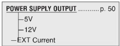

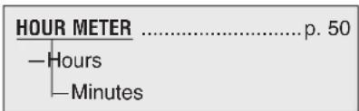
| DRIVER OUTPUT MONITOR MENU | ||
| PARAMETER | ALLOWABLE RANGE | DESCRIPTION |
| Driver1 Current | 0.00–3.50 A | Current sunk by Driver 1. |
| Driver1 PWM | 0.0–100.0 % | PWM % of Driver 1. |
| Driver2 Current | 0.00–1.50 A | Current sunk by Driver 2. |
| Driver2 PWM | 0.0–100.0 % | PWM % of Driver 2. |
| Total Current | 0.00–5.00 A | Total current of both drivers. |
| ANALOG INPUT MONITOR MENU * | ||
| PARAMETER | ALLOWABLE RANGE | DESCRIPTION |
| Voltage type, this variable displays the input voltage value. | ||
| Resistance | 0–7500 Ω | For modules that are configured as resistive input type, this variable displays the input resistance value. |
| Virtual Digital Off, On Virtual digital input state. | ||
* This menu is repeated for Analog Inputs 1–5.
| DIGITAL INPUT MONITOR MENU | ||
| PARAMETER | ALLOWABLE RANGE | DESCRIPTION |
| Input1 | Off, On | Input state of Digital Input 1. |
| Input2 | Off, On | Input state of Digital Input 2. |
| ... | ||
| Input13 | Off, On | Input state of Digital Input 13. |
ENCODER MONITOR MENU
| PARAMETER | ALLOWABLE | |
| RANGE | DESCRIPTION | |
| Pulse Counts | -229 - 229-1 | Current encoder pulse counts. Negative counts indicate the encoder is running in the reverse direction of the zero position. |
| RPM 0 – 65535 rpm Displays RPM, when the encoder typeis☐configured☐as☐RPM☐mode. |
| Position | -32.768–32.767 m | Displays position, when the encoder type is☐con☐gured☐as☐Position☐mode.Negative counts indicate the encoder ia running in the reverse direction of the zero position. |
POWER SUPPLY OUTPUT MONITOR MENU
| PARAMETER | ALLOWABLE RANGE | DESCRIPTION |
| +5V | 0.0–6.3 V | Voltage of the +5V output. |
| +12V | 0.0–16.0 V | Voltage of the +12V output. |
| EXT Current | 0–250 mA | Combined current of the external +12V and +5V power supplies. |
BATTERY VOLTAGE MONITOR MENU
| PARAMETER | ALLOWABLE RANGE | DESCRIPTION |
| Battery Voltage | 0.0–120.0 V | Voltage of the battery. |
HOUR METER MONITOR MENU
| PARAMETER | ALLOWABLE RANGE | DESCRIPTION |
| Hours | 0–65535 h | Present hours of the hour meter. The hour meter runs all the time the 1356 /1356P is powered on. |
| Minutes | 0 – 59 min | Present minutes of the hour meter. |
Fault Menu
The Curtis programmer provides a convenient way to access fault information; see Section 6: Faults and Diagnostics. The programmer displays the faults by name. It displays all faults that are currently set and also a history of all the faults that have been set since the history log was last cleared.
APPENDIX A
DESIGN CONSIDERATIONS
ELECTROMAGNETIC COMPATIBILITY (EMC)
Electromagnetic compatibility (EMC) encompasses two areas: emissions and immunity. Emissions are radio frequency (RF) energy generated by a product. This energy has the potential to interfere with communications systems such as radio, television, cellular phones, dispatching, aircraft, etc. Immunity is the ability of a product to operate normally in the presence of RF energy. EMC is ultimately a system design issue. Part of the EMC performance is designed into or inherent in each component; another part is designed into or inherent in end product characteristics such as shielding, wiring, and layout; and, finally, a portion is a function of the interactions between all these parts. The design techniques presented below can enhance EMC performance in products that use Curtis control products.
Emissions
Signals with high frequency content can produce significant emissions if connected to a large enough radiating area (created by long wires spaced far apart). PWM drivers can contribute to RF emissions. Pulse width modulated square waves with fast rise and fall times are rich in harmonics. (Note: PWM drivers at 100% do not contribute to emissions.) The impact of these switching waveforms can be minimized by making the wires from the controller to the load as short as possible and by placing the load drive and return wires near each other.
For applications requiring very low emissions, the solution may involve enclosing the system, interconnect wires and loads together in one shielded box. Emissions can also couple to battery supply leads and circuit wires outside the box, so ferrite beads near the controller may also be required on these unshielded wires in some applications. It is best to keep the noisy signals as far as possible from sensitive wires.
Immunity
Immunity to radiated electric fields can be improved either by reducing overall circuit sensitivity or by keeping undesired signals away from this circuitry. The controller circuitry itself cannot be made less sensitive, since it must accurately detect and process low level signals from sensors such as the throttle potentiometer. Thus immunity is generally achieved by preventing the external RF energy from coupling into sensitive circuitry. This RF energy can get into the controller circuitry via conducted paths and radiated paths. Conducted paths are created by the wires connected to the controller. These wires act as antennas and the amount of RF energy coupled into them is generally proportional to their length. The RF voltages and currents induced in each wire are applied to the controller pin to which the wire is connected.
The Curtis 1356 /1356P includes bypass capacitors on the printed circuit board's sensitive input signals to reduce the impact of this RF energy on the internal circuitry. In some applications, additional filtering in the form of ferrite beads may also be required on various wires to achieve desired performance levels. A full metal enclosure can also improve immunity by shielding the 1356 /1356P from outside RF energy.
ELECTROSTATIC DISCHARGE (ESD)
Curtis products, like most modern electronic devices, contain ESD-sensitive components, and it is therefore necessary to protect them from ESD (electrostatic discharge) damage. Most of the product's signal connections have protection for moderate ESD events, but must be protected from damage if higher levels exist in a particular application.
ESD immunity is achieved either by providing sufficient distance between conductors and the ESD source so that a discharge will not occur, or by providing an intentional path for the discharge current such that the circuit is isolated from the electric and magnetic fields produced by the discharge. In general the guidelines presented above for increasing radiated immunity will also provide increased ESD immunity.
It is usually easier to prevent the discharge from occurring than to divert the current path. A fundamental technique for ESD prevention is to provide adequately thick insulation between all metal conductors and the outside environment so that the voltage gradient does not exceed the threshold required for a discharge to occur. If the current diversion approach is used, all exposed metal components must be grounded. The shielded enclosure, if properly grounded, can be used to divert the discharge current; it should be noted that the location of holes and seams can have a significant impact on ESD suppression. If the enclosure is not grounded, the path of the discharge current becomes more complex and less predictable, especially if holes and seams are involved. Some experimentation may be required to optimize the selection and placement of holes, wires, and grounding paths. Careful attention must be paid to the control panel design so that it can tolerate a static discharge. MOV, transorbs, or other devices can be placed between B- and offending wires, plates, and touch points if ESD shock cannot be otherwise avoided.
APPENDIX B PROGRAMMING DEVICES
Curtis programmers provide programming, diagnostic, and test capabilities for the 1356 /1356P. The power for operating the programmer is supplied by the host 1356 /1356P via a 4-pin connector. When the programmer powers up, it gathers information from the 1356 /1356P.
Two types of programming devices are available: the 1314 PC Programming Station and the 1313 handheld programmer. The Programming Station has the advantage of a large, easily read screen; on the other hand, the handheld programmer has the advantage of being more portable and hence convenient for making adjustments in the field.
Both programmers are available in User, Service, Dealer, and OEM versions. Each programmer can perform the actions available at its own level and the levels below that—a User-access programmer can operate at only the User level, whereas an OEM programmer has full access.
PC PROGRAMMING STATION (1314)
The Programming Station is an MS-Windows 32-bit application that runs on a standard Windows PC. Instructions for using the Programming Station are included with the software.
HANDHELD PROGRAMMER (1313)
The 1313 handheld programmer is functionally equivalent to the PC Programming Station; operating instructions are provided in the 1313 manual. This programmer replaces the 1311, an earlier model with fewer functions.
PROGRAMMER FUNCTIONS
Programmer functions include:
Parameter adjustment — provides access to the individual programmable parameters.
Monitoring — presents real-time values during vehicle operation; these include all inputs and outputs.
Diagnostics and troubleshooting — presents diagnostic information, and also a means to clear the fault history file.
Programming — allows you to save/restore custom parameter settings.
Favorites — allows you to create shortcuts to your frequently-used adjustable parameters and monitor variables.
APPENDIX C
SPECIFICATIONS
Table C-1 SPECIFICATIONS: 1356 / 1356P MODULE
| Nominal input voltage | 12-36V, 36-80V | |
| Storage ambient temperature range | -40°C to 85°C (-40°F to 185°F) | |
| Operating ambient temp. range | -40°C to 50°C (-40°F to 122°F) | |
| Voltage limits | 12-36V models 36-80V models | |
| Nominal voltage range | 8.5-40V | 25-100V |
| Overvoltage cutoff | >50V | >105V |
| Undervoltage cutoff | <7.5V | <20V |
| Enclosure protection rating | 1356P only: IP65 water/dust immunity (for electronics) | |
| Weight | 1356: 0.05 kg1356P: 0.14 kg | |
| Dimensions (L×W×H) | 1356: 100 × 70 × 16.3 mm1356P: 126 × 80 × 25 mm | |
| EMC | Designed to the requirements of EN 12895: 2000, Industrial Trucks Electromagnetic Compatibility. | |
| Safety | Designed to the requirements of:EN ISO13849-1: 2006 Safety of Machinery, Safety-related Parts of Control System, Part 1,and EN 1175-1:1998+A1: 2010 Safety of Industrial Trucks, Electrical Requirements, Part 1. | |
| MODEL NUMBER VOLTAGE (volts) DESCRIPTION | ||
| 1356-4101 | 12-36 V | No terminal resistor between CAN H and CAN L |
| 1356-4102 | 12-36 V | 120 Ω terminal resistor between CAN H and CAN L |
| 1356-6101 | 36-80 V | No terminal resistor between CAN H and CAN L |
| 1356-6102 | 36-80 V | 120 Ω terminal resistor between CAN H and CAN L |
| 1356P-4101 | 12-36 V | No terminal resistor between CAN H and CAN L |
| 1356P-4102 | 12-36 V | 120 Ω terminal resistor between CAN H and CAN L |
| 1356P-6101 | 36-80 V | No terminal resistor between CAN H and CAN L |
| 1356P-6102 | 36-80 V | 120 Ω terminal resistor between CAN H and CAN L |
- CONTENTS
- FIGURES
- TABLES
- 1
- OVERVIEW
- FEATURES INCLUDE
- DESCRIPTIONS OF KEY FEATURES
- ACTIVE-HIGH DIGITAL INPUTS
- HIGH FREQUENCY DRIVER OUTPUTS
- CONSTANT CURRENT OR VOLTAGE OUTPUTS
- PROGRAMMABLE DITHER FOR HYDRAULIC VALVES
- VOLTAGE ANALOG INPUTS
- RESISTIVE SENSOR INPUTS
- VIRTUAL DIGITAL INPUTS
- ENCODER INTERFACE
- CAN INTERFACE
- PDO DYNAMIC MAPPING
- ONLINE UPDATE
- STATUS LEDS
- 2
- INSTALLATION AND WIRING
- MOUNTING THE MODULE
- CAUTION
- CONNECTIONS
- WIRING RECOMMENDATIONS
- WIRING: BASIC CONFIGURATION
- POWER CONNECTION
- DRIVER OUTPUTS
- SWITCH INPUTS
- ANALOG INPUTS
- CAN BUS
- WIRING: APPLICATION EXAMPLE
- INPUT/OUTPUT SIGNAL SPECIFICATIONS
- DIGITAL INPUTS
- ENCODER INPUTS
- SERIAL PORT
- CAN BUS INTERFACE
- AUXILIARY POWER SUPPLIES
- POWER
- 3
- CANOPEN COMMUNICATIONS
- MINIMUM STATE MACHINE
- BAUD RATES
- CAN NODE ID
- STANDARD MESSAGE IDENTIFIERS
- NMT MESSAGES
- EMERGENCY MESSAGES
- HEARTBEAT
- 4
- PDO COMMUNICATIONS
- OUTPUT COMMAND BYTES
- BDI
- INPUTS 1–13 STATUS BYTES
- VIRTUAL DIGITAL INPUTS BYTE
- ANALOG INPUT HIGH/LOW BYTES
- ENCODER INPUT BYTES
- PULSE COUNT TYPE
- RPM TYPE
- POSITION TYPE
- 5
- SDO COMMUNICATIONS
- SDO MASTER REQUEST (SDO-MOSI)
- SDO 1356 /1356P RESPONSE (SDO-MISO)
- USING AN SDO TO MAP A PDO
- TYPES OF SDO OBJECTS
- COMMUNICATION PROFILE OBJECTS
- TABLE 2 COLUMN DEFINITIONS
- MANUFACTURER'S STATUS REGISTER
- STORE PARAMETER OBJECT
- RESTORE DEFAULT PARAMETERS
- PARAMETER PROFILE OBJECTS
- DRIVER PROPORTIONAL GAIN / DRIVER INTEGRAL GAIN
- ANALOG INPUT ALGORITHMS
- MONITOR PARAMETER PROFILE OBJECTS
- 6
- DIAGNOSTICS AND TROUBLESHOOTING
- FAULT LOG
- 7
- SERIAL COMMUNICATIONS & PROGRAMMING
- PROGRAM MENUS
- MONITOR MENUS
- FAULT MENU
- APPENDIX A
- DESIGN CONSIDERATIONS
- ELECTROMAGNETIC COMPATIBILITY (EMC)
- EMISSIONS
- IMMUNITY
- ELECTROSTATIC DISCHARGE (ESD)
- APPENDIX B PROGRAMMING DEVICES
- PC PROGRAMMING STATION (1314)
- HANDHELD PROGRAMMER (1313)
- PROGRAMMER FUNCTIONS
- APPENDIX C
- SPECIFICATIONS
Brand : CURTIS
Model : 1356
Category : Module d'extension électronique