
BM71 - Bluetooth module Microchip - Free user manual and instructions
Find the device manual for free BM71 Microchip in PDF.


| Product Type | Bluetooth Low Energy (BLE) Module |
| Dimensions | 12.7 mm x 8.7 mm x 1.85 mm |
| Weight | 1.5 g |
| Power Supply | 1.9V to 3.6V DC |
| Operating Temperature | -40°C to +85°C |
| Bluetooth Version | 5.0 |
| Data Rate | 2 Mbps (LE) |
| Antenna | PCB trace antenna |
| Interfaces | UART, SPI, I2C, GPIO |
| Main Functions | Wireless data transmission, BLE connectivity |
| Care and Cleaning | Handle with care; avoid moisture and static discharge |
| Safety | RoHS compliant, CE certified |
| Spare Parts | Not applicable (integrated module) |
| Repairability | Non-repairable; replace if faulty |
| General Information | Microchip BM71 BLE module for IoT applications |
Frequently Asked Questions - BM71 Microchip
User questions about BM71 Microchip
0 question about this device. Answer the ones you know or ask your own.
Ask a new question about this device
Download the instructions for your Bluetooth module in PDF format for free! Find your manual BM71 - Microchip and take your electronic device back in hand. On this page are published all the documents necessary for the use of your device. BM71 by Microchip.
USER MANUAL BM71 Microchip
Note the following details of the code protection feature on Microchip devices:
• Microchip products meet the specifications contained in their particular Microchip Data Sheet.
• Microchip believes that its family of products is secure when used in the intended manner and under normal conditions.
- There are dishonest and possibly illegal methods being used in attempts to breach the code protection features of the Microchip devices. We believe that these methods require using the Microchip products in a manner outside the operating specifications contained in Microchip's Data Sheets. Attempts to breach these code protection features, most likely, cannot be accomplished without violating Microchip's intellectual property rights.
• Microchip is willing to work with any customer who is concerned about the integrity of its code.
- Neither Microchip nor any other semiconductor manufacturer can guarantee the security of its code. Code protection does not mean that we are guaranteeing the product is "unbreakable." Code protection is constantly evolving. We at Microchip are committed to continuously improving the code protection features of our products. Attempts to break Microchip's code protection feature may be a violation of the Digital Millennium Copyright Act. If such acts allow unauthorized access to your software or other copyrighted work, you may have a right to sue for relief under that Act.
Information contained in this publication is provided for the sole purpose of designing with and using Microchip products. Information regarding device applications and the like is provided only for your convenience and may be superseded by updates. It is your responsibility to ensure that your application meets with your specifications.
THIS INFORMATION IS PROVIDED BY MICROCHIP "AS IS". MICROCHIP MAKES NO REPRESENTATIONS OR WARRANTIES OF ANY KIND WHETHER EXPRESS OR IMPLIED, WRITTEN OR ORAL, STATUTORY OR OTHERWISE, RELATED TO THE INFORMATION INCLUDING BUT NOT LIMITED TO ANY IMPLIED WARRANTIES OF NON-INFRINGEMENT, MERCHANTABILITY, AND FITNESS FOR A PARTICULAR PURPOSE OR WARRANTIES RELATED TO ITS CONDITION, QUALITY, OR PERFORMANCE.
IN NO EVENT WILL MICROCHIP BE LIABLE FOR ANY INDIRECT, SPECIAL, PUNITIVE, INCIDENTAL OR CONSEQUENTIAL LOSS, DAMAGE, COST OR EXPENSE OF ANY KIND WHATSOEVER RELATED TO THE INFORMATION OR ITS USE, HOWEVER CAUSED, EVEN IF MICROCHIP HAS BEEN ADVISED OF THE POSSIBILITY OR THE DAMAGES ARE FORESEEABLE. TO THE FULLEST EXTENT ALLOWED BY LAW, MICROCHIP'S TOTAL LIABILITY ON ALL CLAIMS IN ANY WAY RELATED TO THE INFORMATION OR ITS USE WILL NOT EXCEED THE AMOUNT OF FEES, IF ANY, THAT YOU HAVE PAID DIRECTLY TO MICROCHIP FOR THE INFORMATION. Use of Microchip devices in life support and/or safety applications is entirely at the buyer's risk, and the buyer agrees to defend, indemnify and hold harmless Microchip from any and all damages, claims, suits, or expenses resulting from such use. No licenses are conveyed, implicitly or otherwise, under any Microchip intellectual property rights unless otherwise stated.
Trademarks
The Microchip name and logo, the Microchip logo, Adaptec, AnyRate, AVR, AVR logo, AVR Freaks, BesTime, BitCloud, chipKIT, chipKIT logo, CryptoMemory, CryptoRF, dsPIC, FlashFlex, flexPWR, HELDO, IGLOO, JukeBlox, KeeLoq, Kleer, LANCheck, LinkMD, maXStylus, maXTouch, MediaLB, megaAVR, Microsemi, Microsemi logo, MOST, MOST logo, MPLAB, OptoLyzer, PackeTime, PIC, picoPower, PICSTART, PIC32 logo, PolarFire, Prochip Designer, QTouch, SAM-BA, SenGenuity, SpyNIC, SST, SST Logo, SuperFlash, Symmetricom, SyncServer, Tachyon, TimeSource, tinyAVR, UNI/O, Vectron, and XMEGA are registered trademarks of Microchip Technology Incorporated in the U.S.A. and other countries.
AgileSwitch, APT, ClockWorks, The Embedded Control Solutions Company, EtherSynch, FlashTec, HyperSpeed Control, HyperLight Load, IntelliMOS, Libero, motorBench, mTouch, Powermite 3, Precision Edge, ProASIC, ProASIC Plus, ProASIC Plus logo, Quiet-Wire, SmartFusion, SyncWorld, Temux, TimeCesium, TimeHub, TimePictra, TimeProvider, WinPath, and ZL are registered trademarks of Microchip Technology Incorporated in the U.S.A.
Adjacent Key Suppression, AKS, Analog-for-the-Digital Age, Any Capacitor, AnyIn, AnyOut, Augmented Switching, BlueSky, BodyCom, CodeGuard, CryptoAuthentication, CryptoAutomotive, CryptoCompanion, CryptoController, dsPICDEM, dsPICDEM.net, Dynamic Average Matching, DAM, ECAN, Espresso T1S, EtherGREEN, IdealBridge, In-Circuit Serial Programming, ICSP, INICnet, Intelligent Paralleling, Inter-Chip Connectivity, JitterBlocker, maxCrypto, maxView, memBrain, Mindi, MiWi, MPASM, MPF, MPLAB Certified logo, MPLIB, MPLINK, MultiTRAK, NetDetach, Omniscient Code Generation, PICDEM, PICDEM.net, PICkit, PICtail, PowerSmart, PureSilicon, QMatrix, REAL ICE, Ripple Blocker, RTAX, RTG4, SAM-ICE, Serial Quad I/O, simpleMAP, SimpliPHY, SmartBuffer, SMART-I.S., storClad, SQI, SuperSwitcher, SuperSwitcher II, Switchtec, SynchroPHY, Total Endurance, TSHARC, USBCheck, VariSense, VectorBlox, VeriPHY, ViewSpan, WiperLock, XpressConnect, and ZENA are trademarks of Microchip Technology Incorporated in the U.S.A. and other countries.
SQTP is a service mark of Microchip Technology Incorporated in the U.S.A.
The Adaptec logo, Frequency on Demand, Silicon Storage Technology, and Symmcom are registered trademarks of Microchip Technology Inc. in other countries.
GestIC is a registered trademark of Microchip Technology Germany II GmbH & Co. KG, a subsidiary of Microchip Technology Inc., in other countries.
All other trademarks mentioned herein are property of their respective companies.
© 2021, Microchip Technology Incorporated, All Rights Reserved.
ISBN: 978-1-5224-6824-0
For information regarding Microchip's Quality Management Systems, please visit www.microchip.com/quality.
Table of Contents
Chapter 1. Overview
1.1 Operation Overview ...... 15
Chapter 2. Operating Modes, Configuration and Control
2.1 Hardware Interface 63
2.2 BM70/71 Mode Selection 64
2.3 Command Set Protocol 66
2.4 Configuration Protocol 192
2.5 Programming Protocol 193
2.6 Direct Test Protocol 194
Chapter 3. BM70/71 PICtail™/PICtail Plus EVB
3.1 Kit Contents 195
3.2 BM70/71 EVB Features Overview 196
3.3 Hardware Features 201
3.4 Getting Started - BM70/71 EVB Example Configuration 210
3.5 Firmware Programming Procedure 225
A.1 BM70 EVB Reference Schematics 233
B.1 BM71 EVB Reference Schematics 235
C.1 Quick Reference of Host to BM70/71 Module Commands 237
C.2 Quick Reference of BM70/71 Module to Host Event Responses 239
Preface
NOTICE TO CUSTOMERS
All documentation becomes dated, and this manual is no exception. Microchip tools and documentation are constantly evolving to meet customer needs, so some actual dialogs and/or tool descriptions may differ from those in this document. Please refer to our website (www.microchip.com) to obtain the latest documentation available.
Documents are identified with a "DS" number. This number is located on the bottom of each page, in front of the page number. The numbering convention for the DS number is "DSXXXXXXXXA", where "XXXXXXXXX" is the document number and "A" is the revision level of the document.
For the most up-to-date information on development tools, see the MPLAB® X IDE online help. Select the Help menu, and then Topics to open a list of available online help files.
INTRODUCTION
This chapter contains general information that will be useful to know before using the BM70/71 module. Items discussed in this chapter include:
- Document Layout
• Conventions Used in this Guide - Recommended Reading
• The Microchip WebSite
• Product Change Notification Service - Customer Support
• Document Revision History
DOCUMENT LAYOUT
This document describes how to use the BM70/71 module, as a development tool to emulate and debug firmware on a target board. This user's guide is composed of the following chapters:
- Chapter 1. "Overview" provides an overview of the BM70/71 module and its features.
- Chapter 2. "Operating Modes, Configuration and Control" describes the minimum hardware interface required for configuring and controlling the BM70/71 module and the protocols used to communicate with the BM70/71 module.
-
Chapter 3. "BM70/71 PICtail™/PICtail Plus EVB" provides information about various steps involved in configuring the BM70/71 module mounted on the Evaluation Board (EVB) hardware and setting up a connection between the BM70/71 EVB and a smartphone using the Bluetooth Low Energy (Bluetooth Low Energy) link. It also describes various steps involved in downloading the Firmware into the BM70 or BM71 module.
-
Appendix A. "BM70 EVB Schematics" provides the BM70 EVB reference schematics.
- Appendix B. "BM71 EVB Schematics" provides the BM71 EVB reference schematics.
- Appendix C. “Commands Summary Quick Reference” provides the quick references of commands used to/from the host and the BM70/71 module.
CONVENTIONS USED IN THIS GUIDE
This manual uses the following documentation conventions:
DOCUMENTATION CONVENTIONS
| Description Represents Examples | ||
| Italic characters Referenced | books MPLAB IDE User's Guide | |
| Emphasized text ...is the only compiler... | ||
| Initial caps A window the Output window | ||
| A dialog the Settings dialog | ||
| A menu selection select Enable Programmer | ||
| Quotes A field name in a window or dialog | "Save project before build" | |
| Underlined, italic text with right angle bracket | A menu path File > Save | |
| Bold characters A dialog button Click OK | ||
| A tab | Click the Power tab | |
| Text in angle brackets <> | A key on the keyboard | Press,, |
| Plain Courier New | Sample source code | #define START |
| Filenames | autoexec.bat | |
| File paths | c:\mcc18\h | |
| Keywords | _asm,_endasm,static | |
| Command-line options | -Opa+, -Opa- | |
| Bit values | 0, 1 | |
| Constants | 0xFF, 'A' | |
| Italic Courier New | A variable argument | file.o, where file can be any valid filename |
| Square brackets [] | Optional arguments | mccl8 [options] file [options] |
| Curly brackets and pipe character: { | } | Choice of mutually exclusive arguments; an OR selection | errorlevel {0|1} |
| Ellipses... | Replaces repeated text | var_name [, var_name...] |
| Represents code supplied by user | void main (void) { ... } | |
| Notes | A Note presents information that we want to re-emphasize, either to help you avoid a common pitfall or to make you aware of operating differences between some device family members. A Note can be in a box, or when used in a table or figure, it is located at the bottom of the table or figure. | Note: This is a standard note box. |
| CAUTIONThis is a caution note. | ||
| Note 1: This is a note used in a table. | ||
RECOMMENDED READING
This user's guide describes how to use the BM70/71 module. The following Microchip document is available and is recommended as a supplemental reference resource.
BM70/71 Data Sheet (DS60001372)
Refer to this document for detailed information on the BM70/71 module. Reference information found in this data sheet includes:
- BM70/71 module features and pin configurations
• Electrical specifications
• Reference circuits
Bluetooth Core Specification
Refer to this web page for detailed information on Bluetooth Core Specifications at: https://www.bluetooth.com/specifications/bluetooth-core-specification
THE MICROCHIP WEBSITE
Microchip provides online support via our website at: http://www.microchip.com. This website makes files and information easily available to customers. Accessible by most Internet browsers, the website contains the following information:
- Product Support – Data sheets and errata, application notes and sample programs, design resources, user's guides and hardware support documents, latest software releases and archived software
- General Technical Support – Frequently Asked Questions (FAQs), technical support requests, online discussion groups, Microchip consultant program member listings
- Business of Microchip – Product selector and ordering guides, latest Microchip press releases, listings of seminars and events; and listings of Microchip sales offices, distributors and factory representatives
PRODUCT CHANGE NOTIFICATION SERVICE
Microchip's product change notification service helps keep customers current on Microchip products. Subscribers will receive email notification whenever there are changes, updates, revisions or errata related to a specified product family or development tool of interest.
To register, go to www.microchip.com/pcn and follow the registration instructions.
CUSTOMER SUPPORT
Users of Microchip products can receive assistance through several channels:
• Distributor or Representative
- Local Sales Office
• Field Application Engineer (FAE)
- Technical Support
Customers should contact their distributor, representative or Field Application Engineer (FAE) for support. Local sales offices are also available to help customers. A listing of sales offices and locations is included in the back of this document.
Technical support is available through the website at: http://support.microchip.com.
DOCUMENT REVISION HISTORY
Revision B (February 2021)
- Updated the following tables:
- Table 2-5: Updated column headings to Length (H), Length (L), OP Code
- Table 2-6: Removed OP Code column, changed the value of Parameter
- Table2-7: Updated Value of Parameter (3, 4 and 5)
- Table 2-8: Updated column headings to Length (H), Length (L), OP Code
- Table2-13: Updated the Value of OP Code
- Table2-54: Updated the Byte No of Checksum
- Table2-56: Updated the Value of Length (L), and OP Code
- Table2-59: Updated the Value of Parameter
- Table 2-115: Added a new row under Parameter (5)
- Table 2-118: Replaced OP Code with Event OP Code, added new columns of Command OP Code and Command Status
- Updated the following figures:
- Figure 2-24: Interchanged the order of Command Complete and Status Report Events
- Figure 2-25: Added Status Report Event
- Figure 2-55: Replaced with Figure 2-28
- Updated Section 2.3.3.20.4, Section 2.3.3.48.3 and added Section 2.3.3.57
Revision A (October 2016)
• Original release of this document.
Chapter 1. Overview
Microchip's BM70 and BM71 modules are fully certified Bluetooth Low Energy modules. The BM70 and BM71 modules use Microchip's IS1870 and IS1871 chips, respectively. These chips or Integrated Circuits (IC) include the Bluetooth Low Energy RF transceiver, and a certified Bluetooth Low Energy software stack. The BM70/71 module is designed to work with a host microcontroller, generating flexible Bluetooth Low Energy-based functionality to the end target application. The BM70/71 module's operation or behavior is controlled through a set of communication protocols over a UART interface. The target application can gain the following Bluetooth Low Energy-related functionality to control the BM70/71 module by using the commands in these communication protocols:
- Bluetooth core specification features LE Secure Connection (LESC) pairing and LE Data Length Extension:
- Supports LESC pairing methods such as "Just Works", "Passkey Entry", and "Numeric Comparison". The I/O capabilities of the module are configurable to fit with the end target application requirements. The I/O capabilities determine the actual method used for LESC pairing
- Supports LE Data Length extension for up to 104 bytes
- Bluetooth Low Energy Capability – Generic Access Profile (GAP) Roles:
- Broadcaster
- Observer
- Peripheral
- Central
- Bluetooth Low Energy Capability – GAP Modes:
- Broadcast
- Discoverable
- Non-connectable, Directed-connectable, Undirected-connectable
- Bondable
- Bluetooth Low Energy Capability – GAP Procedures:
- Observation
- General-connection establishment
- Connection parameter update
- Terminate connection
- Bonding
- Bluetooth Low Energy Capability – Generic Attribute (GATT) Profile, both GATT Client/Server roles are supported:
- Server configuration
- Service discovery
- Characteristic discovery
- Characteristic descriptor discovery
- Read/Write a characteristic value
- Notification/Indication of a characteristic value
- Reading/Writing a characteristic descriptor
In addition to the Bluetooth Low Energy-related functionality, the module provides a peripheral and general I/O functionality, which can be controlled by using the applicable commands over the UART interface. The available I/O and peripheral features are determined by the specific module being used.
Note: For more information on the I/O and peripheral features of the module, refer to the "BM70/71 Data Sheet" (DS60001372), which is available for download from the Microchip website: www.microchip.com/BM70.
The hardware features enabled by the end target application are determined by the configuration settings applied in the module. This document provides the details regarding various protocols used to configure, control the behavior and program the module.
At a high level, a designer can implement the following work flow when developing a host application with the BM70/71 module:
- If applicable, program the BM70/71 module with the latest firmware (optional, based on end target application requirements)
- To help verify the module placement on a PCB, a designer can invoke the module's test mode to confirm Bluetooth Low Energy output power, as per the Bluetooth Low Energy specification
- Configure the BM70/71 module functionality for the application's requirements
- Once configured, control the BM70/71 Bluetooth Low Energy and hardware behavior by sending the appropriate commands from the host
- During the production stage, a designer can invoke the module's test mode to confirm Bluetooth Low Energy output power, as per the Bluetooth Low Energy specification in their end product
Overall, the designer of the target application is responsible for determining the section(s) of the customizable Bluetooth Low Energy and hardware functionality to be used in the BM70/71 module. Some Bluetooth Low Energy devices are “sources” of data/information while others are “users” of this data/information. The flexibility of the BM70/71 Bluetooth Low Energy solution allows master-central/slave-peripheral devices to be designed and implemented.
It is possible to build a Bluetooth Low Energy product by using multiple different stack splits. The firmware programmed into (or provided for) the BM70/71 module enable users to partition their system so that the embedded application can run on a separate microcontroller (MCU). In this design, the Bluetooth Low Energy controller and host (which runs the Bluetooth Low Energy stack) are in the IS1870/71 chip on the BM70/71 module. Figure 1-1 illustrates an overview of system partitioning with the application running on another chip or microcontroller. Advantages of system partitioning are that the application chip can be very small (i.e., 8-bit microcontroller with a small memory footprint and few resources), or can be a low-powered microcontroller. The interface between the external host chip and the BM70/71 module is a simple UART interface. The communication occurs over the UART through a set of protocols.
Note: In this document, the term "host" will be used to refer to the chip/microcontroller which runs the applications. The term "host" does not mean the internal Bluetooth Low Energy host controller of the IS1870/71 already present in the IC.
FIGURE 1-1: BM70/71 MODULE OPERATION OVERVIEW

flowchart
graph TD
    A["Microchip BM70"] --> B["Application"]
    B --> C["Microcontroller or PC"]
    C --> D["UART"]
    D --> E["General Access Profile (GAP)"]
    D --> F["General Attribute Profile (GATT)"]
    D --> G["Attribute (ATT) Protocol"]
    D --> H["Logical Link Control and Adaptation Protocol (L2CAP)"]
    D --> I["Host Controller Interface (HCI)"]
    D --> J["Link Layer"]
    D --> K["Physical Layer (PHY)"]
    D --> L["Direct Test Mode"]
    M["IS187x chip"] --> N["Host"]
    M --> O["Controller"]
The BM70/71 module has configurable hardware and Bluetooth Low Energy functionality. The user can configure the functionality required from the BM70/71 module to meet the end target application's requirements. The BM70/71 module operation is governed by the configuration settings applied by the host. This section provides the details of all the possible functions that the host can apply to the BM70/71 module.
1.1.1 Configuration Overview
Configuring the BM70/71 module involves putting the device in Configure mode, and sending commands over the UART interface from the configuration protocol to enable/disable functionality. This configuration is stored in non-volatile memory, so the settings are retained even after a power cycle and they remain in effect until there is a change. After configuring the BM70/71 module, the host will need to put the module in Application/Run mode, and send commands over the UART interface from the "Command Set" protocol to control the Bluetooth Low Energy and hardware functions over the UART interface. For more information on switching between modes and communication protocols, refer to Chapter 2. "Operating Modes, Configuration and Control".
1.1.2 System Operation
The BM70/71 module has two main configuration options which affect the overall Bluetooth Low Energy and hardware behavior available to the host. The two configurations are:
- Auto Operation Configuration: Auto Operation restricts the available Bluetooth Low Energy operation by only allowing the Bluetooth Low Energy peripheral to act as a raw data pipe. This is compatible with hosts who only require the BM70/71 module to act as a virtual UART cable between the host and the remote peer device
- Manual Operation Configuration: Manual Operation provides the host the most functionality and control over the BM70/71 Bluetooth Low Energy protocol and operation. This configuration is used by a host to leverage the flexibility and feature set offered by both the Bluetooth Low Energy protocol and the BM70/71 module
Figure 1-2 illustrates the internal logic of the BM70/71 module as a state machine with three states. Each state handles a specific portion of the overall Bluetooth Low Energy operation. When the host chooses Auto Operation or Manual Operation, the following occurs:
- The number of events processed by the BM70/71 module in each state is determined
• The way events are generated by the host is determined
Auto Operation has a reduced number of events in each state because the available Bluetooth Low Energy functionality is restricted. The events are generated by the host indirectly through values, which are setup in Configuration mode.
Manual Operation allows more events to occur in each state because more Bluetooth Low Energy functionality is available. The events are directly generated by the host through commands sent over the UART.
FIGURE 1-2: STATE MACHINE DIAGRAM

flowchart
graph TD
    A["Auto Operation (AO)"] --> B["Standby state"]
    C["Manual Operation (MO)"] --> D["Event in MO to cause State Transition"]
    B --> E["Event_Y"]
    B --> F["Event_X"]
    D --> G["Link state"]
    E --> H["Shutdown state"]
    F --> H
    G --> H
    H --> I["●"]
    style A fill:#f9f,stroke:#333
    style C fill:#f9f,stroke:#333
    style B fill:#ccf,stroke:#333
    style D fill:#ccf,stroke:#333
    style E fill:#cfc,stroke:#333
    style F fill:#cfc,stroke:#333
    style G fill:#fcc,stroke:#333
    style H fill:#fcc,stroke:#333
The designer of the end target application selects the applicable configuration: Auto Operation or Manual Operation. The designer also determines the available hardware functionality to be used. This complete configuration is programmed into the BM70/71 module by the host. Once configured, the host can switch the module to Run mode and perform the Bluetooth Low Energy operations. Figure 1-3 illustrates the overview of the BM70/71 module system operation.
FIGURE 1-3: BM70/71 MODULE SYSTEM OPERATION

flowchart
graph TD
    A["Power-on / Reset"] --> B{Configure Mode or Run Mode}
    B -->|Reset| C["Configure BM70/71"]
    B -->|Configure Mode| D["Manual Operation or Auto Operation"]
    D --> E["Auto Operation"]
    D --> F["Manual Operation"]
For additional information about the Bluetooth Low Energy and hardware-related functions, refer to 1.1.2.1 "Auto Operation" and 1.1.2.2 "Manual Operation".
1.1.2.1 AUTO OPERATION
Auto Operation limits the available Bluetooth Low Energy and hardware functionality, but is the simplest configuration to use. The intended target application Auto Operation is a raw data pipe between the host and the Bluetooth Low Energy central/master device (peer device). Before two devices can exchange data, they must first find each other and connect. In Bluetooth Low Energy, the GAP layer defines how two devices find each other, discover what each device can do, and how they are able to repeatedly find and connect with each other. Using the roles defined by the GAP layer, the BM70/71 module will only behave as a peripheral advertising, using connectable advertising packets. The BM70/71 module uses the Limited-Discoverable mode and General-Discoverable mode defined in the GAP to make its presence known while Auto Operation is active. Once connected, a private GATT service called "Transparent UART" is used to exchange data with the peer device. This simplifies the tasks a host has to do when trying to communicate data over Bluetooth Low Energy. Auto Operation works well for hosts who do not care about the Bluetooth Low Energy protocols, but want the BM70/71 module to act as a virtual UART pipe between the host and the Bluetooth Low Energy central/master. When Auto Operation is active, any data sent over the UART interface is transmitted to the connected device. Any data received by the BM70/71 module from the connected device is sent over the UART interface to the host. This means the "Command Set" protocol, used to control the BM70/71 module operation, is ignored. When Auto Operation is active, any "Command Set" protocol messages sent by the host will not be interpreted. Instead, the data will be transmitted to the connected Bluetooth Low Energy device.
Because Auto Operation does not accept the "Command Set" protocol message over the UART, there are additional configuration options available. These additional options allow the host to get the BM70/71 module status and to generate events to gain some control over the BM70/71 module behavior.
Table 1-1 provides the BM70/71 functionality and configuration options available when used in Auto Operation.
TABLE 1-1: FUNCTIONALITY AND CONFIGURATION OPTIONS
| Configuration Item | Related Parameters | Related Hardware Pins | Section Reference Description |
| Status Indication | N/A Status1_IND | Status2_IND | 1.1.2.1.2 “Auto Operation – Status Indication” |
| Run Time Configuration Window | Configuration Timeout N/A 1.1.2.1.3 | “Auto | Operation – Configuration Timeout” |
| UART Flow Control | N/A RTS | CTS | 1.1.2.1.4 “Auto Operation – UART Flow Control” |
| Connection Settings | Minimum Connection Interval Maximum Connection Interval Slave Latency Supervision Timeout | N/A 1.1.2.1.11 | “Auto Operation – Connections” |
| Discoverability Settings | Fast Advertising Interval Reduced Power Advertising Interval Fast Advertising Timeout Reduced Power Advertising Timeout Standby Period after Power On Standby Period after Disconnect | N/A 1.1.2.1.10 | “Auto Operation – Discoverability” |
TABLE 1-1: FUNCTIONALITY AND CONFIGURATION OPTIONS
| Configuration Item | Related Parameters | Related Hardware Pins | Section Reference Description |
| Advertising Data | Manufacture dataDevice NameUUIDs | N/A | |
| Scan Response Data | Manufacture DataBattery Level IndicationTX Power SettingUser Specific Data | N/A | |
| Link Quality Indication | Normal Received Signal Strength Indication (RSSI) Threshold LevelWeak RSSI Threshold Level | RSSI_IND 1.1 | 2.1.8 “AutoOperation – LinkQuality Indication” |
| Low Battery Indication | Low Battery LevelBattery Detection ThresholdNormal Battery LevelLow Battery Timeout Period | LOW_BATTERY_IND | 1.1.2.1.7 “AutoOperation – LowBattery Indication” |
| BM70/71 Active Indication | Indication Type RX_ACTIVE | _IND | 1.1.2.1.9 “AutoOperation –BM70/71 ActiveIndication” |
| Disconnect Link Enter Standby | N/A PAIRING_KEY 1.1.2.1.5 “Auto | Operation – Pairing Key” | |
| Disconnect Link Enter Shutdown | N/A LINK_DROP 1.1.2.1.6 “Auto | Operation – Link Drop” |
Some of the configuration options (Table 1-1) are available for the host to control in Manual Operation through the "Command Set" protocol. The options listed in Table 1-1 are available when the Auto Operation configuration is chosen.
The internal logic of the BM70/71 module executes as a state machine (refer to 1.1.2 "System Operation"). Each state has parameters, which can be configured (see Table 1-1), to determine the behavior in Auto Operation. These configuration options allow the host to perform the following:
- Instruct when transitions between the states will occur
- Force transitions to different states by using hardware pins to generate events
- Indicate when a state transition occurs
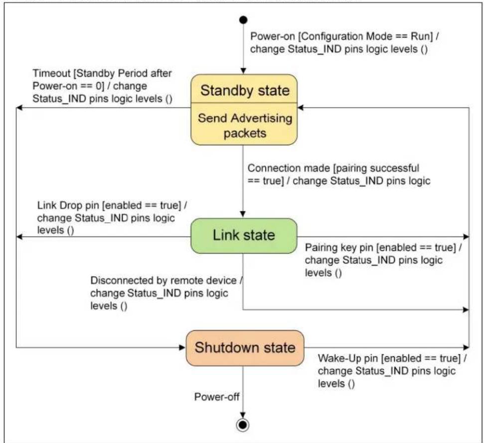
Figure 1-4 illustrates the state machine diagram behavior when Auto Operation is active.
FIGURE 1-4: STATE MACHINE IN AUTO OPERATION MODE
flowchart
graph TD
    A["Power-on [Configuration Mode == Run"] / change Status_IND pins logic levels()] --> B["Standby state"]
    B --> C["Send Advertising packets"]
    C --> D["Link state"]
    D --> E["Link Drop pin [enabled == true"] / change Status_IND pins logic levels()]
    D --> F["Disconnected by remote device / change Status_IND pins logic levels()"]
    D --> G["Power-off"]
    G --> H["Shutdown state"]
    H --> I["Wake-Up pin [enabled == true"] / change Status_IND pins logic levels()]
    B --> J["Timeout [Standby Period after Power-on == 0"] / change Status_IND pins logic levels()]
    D --> K["Connection made [pairing successful == true"] / change Status_IND pins logic]
    K --> L["Pairing key pin [enabled == true"] / change Status_IND pins logic levels()]
    L --> M["Shutdown state"]
The host should be aware of the logic in each state which is automatically executed by the BM70/71 module while Auto Operation is active. The BM70/71module does not wait for the host to control this behavior. The following is a description of each state:
- Standby state – This state is where the BM70/71 module is in Bluetooth discoverable and connectable mode. The module enables Undirected Advertising, and can be paired by another device as long as the module remains in Discoverable and Connectable mode. The information sent in the Advertising packets and Scan Response packets are determined at the time of configuration. The pairing process takes place in this state and, if successful, the BM70/71 module will transition to the Link state.
- Link state – In this state the BM70/71 module has an active connection with a Remote Bluetooth Low Energy device. The host can send/receive data to/from the remote device
- Shutdown state – This state is where the BM70/71 module enters a deep-sleep power mode. There is no active RF communication taking place and the current draw by the BM70/71 module is the lowest. The host must bring the BM70/71 module out of this state if the host wants to communicate with a remote device.
1.1.2.1.1 Auto Operation – Transparent UART
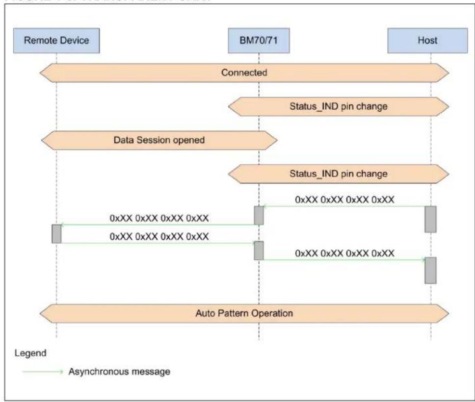
When Auto Operation is active, the Bluetooth Low Energy capabilities of the BM70/71 module are reduced to simplify the operation. The BM70/71 module can only take on the GAP role of the peripheral and, once connected, the module can only become a slave. In this role, it can operate as a "raw data exchanger" between the host and remote central Bluetooth Low Energy device. The BM70/71 module will format the received UART data from the host as ATT packets, send them to the remote device, and the data from the peer device is unpacked by the module. This data exchange protocol will go through a proprietary service, referred to as the "Transparent UART Service". From the host point of view, data can be sent and received over the UART directly (without being processed by the Bluetooth module), once the "Transparent UART Service" is enabled. This is the only Bluetooth Low Energy capability available when the BM70/71 module has been configured for Auto Operation.
Figure 1-5 illustrates the sequence diagram for the flow of data between a Remote Bluetooth Low Energy device, the BM70/71 module, and the host.
FIGURE 1-5: TRANSPARENT UART
flowchart
graph TD
    A["Remote Device"] --> B["Connected"]
    B --> C["Status_IND pin change"]
    C --> D["Data Session opened"]
    D --> E["Status_IND pin change"]
    E --> F["Auto Pattern Operation"]
    F --> G["0xXX 0xXX 0xXX 0xXX"]
    F --> H["0xXX 0xXX 0xXX 0xXX"]
    G --> I["0xXX 0xXX 0xXX 0xXX"]
    H --> J["0xXX 0xXX 0xXX 0xXX"]
    style A fill:#cce5ff,stroke:#333
    style B fill:#ffcccc,stroke:#333
    style C fill:#ffcccc,stroke:#333
    style D fill:#ffcccc,stroke:#333
    style E fill:#ffcccc,stroke:#333
    style F fill:#ffcccc,stroke:#333
    style G fill:#ffcccc,stroke:#333
    style H fill:#ffcccc,stroke:#333
    style I fill:#e6f7ff,stroke:#333
    style J fill:#e6f7ff,stroke:#333
1.1.2.1.2 Auto Operation – Status Indication
The host can no longer send or receive a “Command Set” protocol message to find out the BM70/71 module’s Bluetooth Low Energy status because the UART interface becomes a data pipe between the host and Bluetooth Low Energy central/master. To overcome this issue when using Auto Operation, two hardware pins can take on the functionality to indicate the BM70/71 module’s status to the host. The logic level on these two hardware pins can be sampled by the host to gain the Bluetooth Low Energy status information (see Figure 1-6). Table 1-2 provides the details of the Status indication pins.
TABLE 1-2: STATUS INDICATION PINS
| Status1_IND/Status2_IND | Status Description | |
| H/H Shutdown | mode | The BM70/71 module is in shutdown mode; the module enters into a deep-sleep mode. For more details, refer to 1.1.2.3.2 “General Operation – Low Power Control” |
| H/L Standby mode | The BM70/71 module | is sending advertising packets and is waiting for a connection. The module is discoverable and connectable |
| L/L Bluetooth Low Energy-connected mode | The Bluetooth Low Energy link is established and the Client Characteristic Configuration Descriptor (CCCD) of “ISSC_Transparent_TX” characteristic is disabled | |
| L/H Data Sess | on open The Bluetooth Low Energy link is established and the CCCD of “ISSC_Transparent_TX” characteristic is enabled | |
FIGURE 1-6: STATUS INDICATION

flowchart
graph LR
    A["Status1_IND"] --> B["Power-on state"]
    B --> C["Standby state"]
    C --> D["Connected"]
    D --> E["Data Session Open"]
    E --> F["Standby state"]
    F --> G["Shutdown state"]
    H["Status2_IND"] --> I["Power-on state"]
    I --> J["Standby state"]
    J --> K["Connected"]
    K --> L["Data Session Open"]
    L --> M["Standby state"]
    M --> N["Shutdown state"]
Table 1-3 provides the list of the pins in the BM70/71 module which can be configured to operate with this functionality.
TABLE 1-3: CONFIGURATION OF STATUS INDICATION PINS
| Functionality BM70 PINS BM71 PINS | |||
| Status1_IND P00 (if | CTS is disabled) | P00 (if CTS is disabled) | |
| P07 | P12 | ||
| P10 | P13 | ||
| P11 | P16 | ||
| P12 | P17 | ||
| P13 | P36 (if RTS is disabled) | ||
| P22 | |||
| P24 | |||
| P31 | |||
| P32 | |||
| P33 | |||
| P34 | |||
| P35 | |||
| P36 (if RTS is disabled) | |||
| Status2_IND P00 (if | CTS is disabled) | P00 (if CTS is disabled) | |
| P07 | P12 | ||
| P10 | P13 | ||
| P11 | P16 | ||
| P12 | P17 | ||
| P13 | P36 (if RTS is disabled) | ||
| P22 | |||
| P24 | |||
| P31 | |||
| P32 | |||
| P33 | |||
| P34 | |||
| P35 | |||
| P36 (if RTS is disabled) | |||
1.1.2.1.3 Auto Operation – Configuration Timeout
When Auto Operation is active, the "Command Set" protocol will be ignored. In order to make changes to some of the features in the BM70/71 module behavior (available in Auto Operation mode), before the module enters the Auto operation mode, a window of time, called the Configuration Timeout, is provided. This Configuration Timeout value is set in Configuration mode. During this time period, the host can send applicable "Command Set" protocol messages over the UART to alter the BM70/71 Bluetooth Low Energy behavior.
Figure 1-7 illustrates system operation when the BM70/71 module has been configured to have a "Configuration Window" open before Auto Operation becomes active.
FIGURE 1-7: BM70/71 MODULE CONFIGURATION TIMEOUT

flowchart
graph TD
    A["Power-on / Reset"] --> B{Configure Mode or Run Mode}
    B -->|Run Mode| C["Configuration Window – “Command Set Protocol” available"]
    C --> D{Configuration Window Timeout}
    D -->|No| E["Configure BM70/71"]
    E --> B
    D -->|Yes| F["Auto Operation"]
    G["Configure BM70/71"] --> B
The configuration option is an 8-bit value and each bit represents a unit of 640 ms. A value of "0" disables the "Configuration Window". The following formula can be used to calculate the timeout period of the "Configuration Window":
Timeout Value = (x * 0.640), where x is the programmable value in the range 1 to 255.
FIGURE 1-8: CONFIGURATION TIMEOUT DISABLED

flowchart
graph TD
    A["Host"] --> B["Reset"]
    B --> C["Auto Pattern Operation"]
    C --> D["Configure Mode Status (enabled)"]
    D --> E["Any valid command"]
    E --> F["Configure Mode Status (Timeout occurred - disabled)"]
    F --> G["Configure Mode Period"]
    G --> H["BM70/71"]
    style A fill:#e6f3ff,stroke:#333
    style B fill:#e6f3ff,stroke:#333
    style C fill:#e6f3ff,stroke:#333
    style D fill:#e6f3ff,stroke:#333
    style E fill:#e6f3ff,stroke:#333
    style F fill:#e6f3ff,stroke:#333
    style G fill:#e6f3ff,stroke:#333
    style H fill:#e6f3ff,stroke:#333
If the configuration timeout window is enabled by the host, the host can also command the BM70/71 module to exit the configuration period early, if necessary. Figure 1-9 illustrates the sequence diagram (for more information on "Command Set" protocol messages, refer to 2.3.3 "Commands and Event Responses").
FIGURE 1-9: CONFIGURATION ENDED BY HOST

flowchart
graph TD
    A["Host"] --> B["Reset"]
    B --> C["Auto Pattern Operation"]
    C --> D["Configure Mode Status (enabled)"]
    D --> E["Any valid command"]
    E --> F["Leave Configure Mode"]
    F --> G["Command Complete"]
    G --> H["BM70/71"]
    H --> I["Configure Mode Period"]
    I --> J["Legend"]
    style A fill:#cce5ff,stroke:#333
    style B fill:#cce5ff,stroke:#333
    style C fill:#cce5ff,stroke:#333
    style D fill:#e6f2ff,stroke:#333
    style E fill:#e6f2ff,stroke:#333
    style F fill:#e6f2ff,stroke:#333
    style G fill:#e6f2ff,stroke:#333
    style H fill:#e6f2ff,stroke:#333
    style I fill:#e6f2ff,stroke:#333
    style J fill:#e6f2ff,stroke:#333
1.1.2.1.4 Auto Operation – UART Flow Control
The BM70/71 module supports UART flow control. When flow control is enabled, the CTS and RTS pins become active. Flow control is used to prevent temporary UART buffer overrun in the host and/or the BM70/71 module. If the UART buffer of the BM70/71 module is full, RTS will be raised by the module. If the UART buffer of the host is full, CTS of the module (RTS pins of the host) will be raised by the host. At most two bytes are sent after CTS is raised.
Figure 1-10 and Figure 1-11 illustrate the functionality of UART CTS flow control and UART RTS flow control.
FIGURE 1-10: UART CTS FLOW CONTROL

FIGURE 1-11: UART RTS FLOW CONTROL

Table 1-4 provides the list of the available BM70/71 module pins that can be used for the flow control functionality.
TABLE 1-4: PINS FOR FLOW CONTROL FUNCTIONALITY
| Functionality BM70 PINS BM71 PINS | |
| CTS P00 P00 | |
| RTS P13 P36 |
1.1.2.1.5 Auto Operation – Pairing Key
When the BM70/71 module is connected to a remote device and in the Link state, the host can use the pairing key to force the module to disconnect the link and go back to the Standby state. In the Standby state, the module effectively starts to advertise again. All the timeouts associated with the Standby state restart at their configured value and become active.
The Pairing Key is a configurable hardware pin that the host can use to indicate to the BM70/71 module to exit the Link state and return to the Standby state. Figure 1-12 illustrates how the host can use this functionality.
FIGURE 1-12: PAIRING KEY

The host must drive the configured pin to be the Pairing Key to a logic level of "0" for >= 160 ms (TPAIRING_KEY). Table 1-5 provides the list of the hardware pins available for the Pairing Key functionality.
TABLE 1-5: PINS FOR PAIRING KEY FUNCTIONALITY
| Functionality BM70 PINS BM71 PINS | ||
| Pairing Key | P00 (if CTS disabled) | P00 (if CTS disabled) |
| P07 | P12 | |
| P10 | P13 | |
| P11 | P16 | |
| P12 | P17 | |
| P13 | P36 (if RTS disabled) | |
| P22 | ||
| P24 | ||
| P31 | ||
| P32 | ||
| P33 | ||
| P34 | ||
| P35 | ||
| P36 (if RTS disabled) | ||
1.1.2.1.6 Auto Operation – Link Drop
When the BM70/71 module is connected to a remote device and is in the Link state, the host can use Link Drop to force the module to disconnect the link and transition to the Shutdown state. In the Shutdown state, the BM70/71 module enters into a deep-sleep mode, there is no RF activity and then the UART is disabled. The module will remain in this state until a power loss event or the host wakes the BM70/71 module. Figure 1-13 illustrates how the host can use this functionality.
FIGURE 1-13: LINK DROP

The host must drive the pin configured to be the Link Drop to a logic level of "0" for >= 10 ms (TLINK_DROP). Table 1-6 provides the details of the hardware pins available for this functionality.
TABLE 1-6: PINS FOR LINK DROP FUNCTIONALITY
| Functionality BM70 PINS BM71 PINS | |
| Link Drop P00 (if CTS is disabled) | P00 (if CTS is disabled) |
| P07 | P12 |
| P10 | P13 |
| P11 | P16 |
| P12 | P17 |
| P13 | P36 (if RTS is disabled) |
| P22 | |
| P24 | |
| P31 | |
| P32 | |
| P33 | |
| P34 | |
| P35 | |
| P36 (if RTS is disabled) |
1.1.2.1.7 Auto Operation – Low Battery Indication
Because the host cannot get a status from the BM70/71 module regarding the battery voltage level over the UART, the host can configure the module to use a hardware pin to indicate when certain voltage thresholds have been detected on the BAT_IN pin of the module. The voltage thresholds used by this function are configurable. Figure 1-14 illustrates how the host can use the Low Battery Indication pin to detect the configured battery voltage levels.
FIGURE 1-14: LOW BATTERY INDICATION

When the BM70/71 module detects that the battery voltage is lower than the "Low Battery Level" threshold, LOW_BATTERY_IND will be driven to logic level "0". When the BM70/71 module detects the battery voltage is >= "Normal Battery Level" threshold, LOW_BATTERY_IND will be driven to logic level "1". The BM70/71 module can be configured to enter the Shutdown state if the battery voltage is lower than the "Low Battery Level" threshold for a certain time period. This time period is referred to as Low Battery into Shutdown time. The rate at which the BM70/71 module samples the battery voltage level is configurable, and referred to as the Battery Detection Interval. The following formulas can be used to calculate the associated time periods and voltage levels:
Battery Detection Interval = (x * 0.08), where x is the programmable value
Low Battery Into Shutdown Time = (x * 0.64), where x is the programmable value Battery Level (Low, Normal) = (x * 0.1), where x is the programmable value
Table 1-7 provides the information of the battery level functionality.
TABLE 1-7: BATTERY LEVEL FUNCTIONALITY
| Functionality Parameter Range Parameter Value | |
| Battery Detection Interval 0x01-0xFF Each bit represents a unit of 80 msInterval = x * 80 ms | |
| Low Battery Level 0x00-0x12 Each bit represents a unit of 100 mVThreshold = x * 100 mV | |
| Normal Battery Level | 0x00-0x12 Each bit represents a unit of 100 mVThreshold = x * 100 mV |
| Low Battery into Shutdown Time | 0x00-0xFF Each bit represents a unit of 640 msInterval = x * 640 msA value of “0” disables this functionality |
Table 1-8 provides list of the hardware pins that can be used for the LOW_BATTERY_IND functionality.
TABLE 1-8: PINS FOR LOW_BATTERY_IND FUNCTIONALITY
| Functionality BM70 PINS BM71 PINS | ||
| LOW_BATTERY_IND | P00 (if CTS is disabled) | P00 (if CTS is disabled) |
| P07 | P12 | |
| P10 | P13 | |
| P11 | P16 | |
| P12 | P17 | |
| P13 | P36 (if RTS is disabled) | |
| P22 | ||
| P24 | ||
| P31 | ||
| P32 | ||
| P33 | ||
| P34 | ||
| P35 | ||
| P36 (if RTS is disabled) | ||
1.1.2.1.8 Auto Operation – Link Quality Indication
The BM70/71 module indicates the quality of the RF link by providing a number referred to as the RSSI value. When Auto Operation is active, the host cannot retrieve this number because the UART interface becomes a data pipe and all "Command Set" protocol messages are ignored. If the Link Quality Detection option is enabled by the host during Configuration mode, the BM70/71 module can indicate the quality of the link using a hardware pin. The host provides two threshold values, which the module uses to compare against the current RSSI measurement. If the module measured RSSI value is above or below these two threshold values, then the respective hardware pin is driven to a logic level of "0" or "1". This gives the host an idea of the link quality, and determines a good link and a poor link in the configuration mode.
Figure 1-15 illustrates the sequence diagram of the Link Quality Indication.
FIGURE 1-15: LINK QUALITY INDICATION
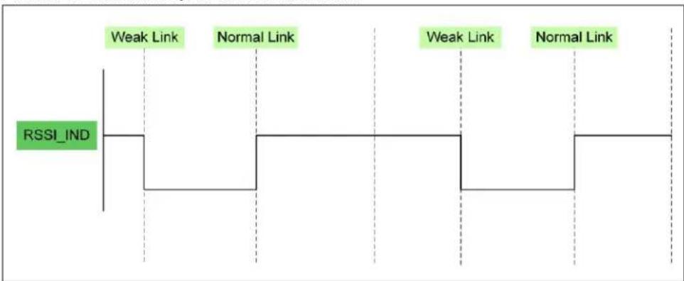
The rate at which the BM70/71 module can change the RSSI_IND pin to indicate link quality is based off of the connection interval controlled by the Remote Bluetooth Low Energy central device. Approximately 25 ms is the quickest the BM70/71 module can measure the RSSI value, then compare it to the configured thresholds, and finally drive the RSSI_IND pin to the appropriate logic level.
Table 1-9 provides the details of the possible configuration ranges the host can set with the BM70/71 module.
TABLE 1-9: CONFIGURATION RANGE
| Functionality Parameter Range Parameter Value | |
| Normal RSSI Threshold 0x32 | 2-0x5A Represented as a decibel (dB) |
| Weak RSSI Threshold 0x32 | 2-0x5A Represented as a decibel (dB) |
Table 1-10 provides the list of the available hardware pins that can be used as the RSSI_IND pin.
TABLE 1-10: PINS FOR RSSI_IND FUNCTIONALITY
| Functionality BM70 PINS | BM71 PINS | |
| RSSI_IND | P00 (if CTS is disabled) | P00 (if CTS is disabled) |
| P07 | P12 | |
| P10 | P13 | |
| P11 | P16 | |
| P12 | P17 | |
| P13 | P36 (if RTS is disabled) | |
| P22 | ||
| P24 | ||
| P31 | ||
| P32 | ||
| P33 | ||
| P34 | ||
| P35 | ||
| P36 (if RTS is disabled) | ||
1.1.2.1.9 Auto Operation – BM70/71 Active Indication
The host can get the status of the module when the BM70/71 module internal MCU is operating and/or when the physical layer (i.e., Radio) is operating. This information is useful if the host needs to know whether the BM70/71 module is in any of the low-power modes. When Auto Operation is active, the host cannot retrieve this information using the "Status Report" command in the "Command Set" protocol. Therefore, the BM70/71 module provides a way to indicate activity over a hardware pin.
This type of activity is configurable; the host can choose to be notified if the internal BM70/71 MCU/internal Radio is active, or if just the internal Radio is active. Based on the activity indication, the BM70/71 module will drive the RF_ACTIVE_IND pin to a logic level of "1" if the activity indication is "true" (see Figure 1-16), or to a logic level of "0" if the activity indication is "false" (see Figure 1-17).
FIGURE 1-16: BM70/71 ACTIVE INDICATION

FIGURE 1-17: BM70/71 ACTIVE INDICATION
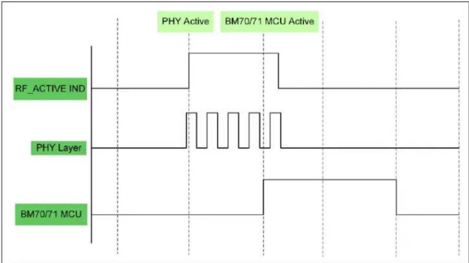
Table 1-11 provides the possible configuration ranges the host can set the BM70/71 module to.
TABLE 1-11: BM70/71 CONFIGURATION RANGE
| Functionality Parameter Range Parameter Value | |
| BM70/71 Active Indication 0x00-0x01 Disabled/Enabled | |
| Activity Indication Type 0x00-0x01 RF, Physical Layer Only /RF, Physical Layer + MCU |
Table 1-12 provides the list of the available hardware pins that can be used as the RF_ACTIVE_IND pin.
TABLE 1-12: PINS FOR RF ACTIVE IND FUNCTIONALITY
| Functionality BM70 PINS BM71 PINS | ||
| RF_ACTIVE_IND P00 (if | CTS is disabled) | P00 (if CTS is disabled) |
| P07 | P12 | |
| P10 | P13 | |
| P11 | P16 | |
| P12 | P17 | |
| P13 | P36 (if RTS is disabled) | |
| P22 | ||
| P24 | ||
| P31 | ||
| P32 | ||
| P33 | ||
| P34 | ||
| P35 | ||
| P36 (if RTS is disabled) | ||
1.1.2.1.10 Auto Operation – Discoverability
To exchange data over Bluetooth Low Energy, devices must have the capability of finding each other first. When Auto Operation is active, the BM70/71 module can only take on the role of a peripheral (defined in the GAP layer), and a peripheral makes its presence known by following certain rules in Bluetooth Low Energy. A device's discoverability refers to how the peripheral advertises its presence to other devices and what those devices are able to do with the information. When Auto Operation is active, the BM70/71 module can only use the GAP layer's defined discoverable modes. It cannot be a scanner and use discovery procedures. The values provided during the configuration of the BM70/71 module affects how another device can detect the presence of the BM70/71.
In Auto Operation, the BM70/71 module is in the general discoverable mode. It will advertise as long as the "advertising time" value is configured for. Advertising packets ADV_IND are the only type sent. This means the device is in Undirected-Connectable mode, making itself connectable. The host has no control over this in Auto Operation; this is the only behavior allowed.
The host has control over the time-related values, like how long and how fast the BM70/71 module will advertise. These values are set at the time of configuration and are as follows:
- Fast Advertising Interval – This is the initial advertising interval (T advertising_interval) used when the BM70/71 module enters Standby mode in the Standby state (see Figure 1-2). The faster the device advertises, the quicker it can be discovered. However, the device will consume more current since it is actively transmitting
- Fast Advertising Timeout – This is the period of time the BM70/71 module will send the advertising packets at the Fast Advertising Interval rate
-
Reduced Power Advertising Interval – This is the secondary advertising interval (TReduced_Power_Advertising_Interval). It is meant to allow the device to be discovered, but sends the advertising packets at a slower rate to help conserve power. This time interval will only start if the configured “Fast Advertising Timeout” period has expired. The name of this interval “Reduced Power Advertising” does not change or alter anything related to transmit power when sending advertising packets. This term is meant to imply the overall power consumption of the BM70/71 module is reduced because the rate at which the packets are sent is slower.
-
Reduced Power Advertising Timeout – This is the period of time the BM70/71 module will send advertising packets at the “Reduced Power Advertising Interval” rate. Once this time period expires and if the BM70/71 module has not made a connection, the BM70/71 module will automatically enter the Shutdown state where it will be enter into the low-power, “Deep-sleep/Shutdown” mode. This value is calculated internally by the BM70/71 module. The calculated value is based on either the “Standby Time” or the “After Disconnect Standby Time” parameter and the “Fast Advertising Timeout” parameter (for calculating using the formula, refer to Table 1-13).
- Standby Time – This is the total period of time the BM70/71 module will advertise. This value is used after RST_N hardware of a Power-on Reset (POR) event to determine how long the BM70/71 module will advertise in the Standby state.
- After Disconnect Standby Time – This time period becomes relevant after the BM70/71 module receives a disconnect event. The BM70/71 module has to be in the Link state, then must receive a disconnect event (from host or peer device), and then move into the Standby state (see Figure 1-2). When entering the Standby state from the Link state, the BM70/71 module is able to use the “After Disconnect Standby Time” period value to determine the total advertising time. This value will override the “Standby Time” value that is used when the BM70/71 module enters the Standby state for the first time. If this parameter is non-zero, and the conditions are met for using this value, the “Reduced Power Advertising Timeout” value will be calculated using this parameter.
Table 1-13 provides the configuration values which impact the BM70/71 module behavior while sending the advertising packets.
TABLE 1-13: CONFIGURATION VALUES FOR DISCOVERABILITY
| Functionality Parameter Range Parameter Value | ||
| Fast Advertising Interval | 0x0020-0x4000 | Each bit represents 625 μsInterval = x * 0.000625 |
| Fast Advertising Timeout 0x00-0xFF Each bit represents 10.24sInterval = x * 10.24A value of 0x00 disables this timeout period. If disabled, the BM70/71 module will never exit the “Fast Advertising Interval” | ||
| Reduced Power Advertising Interval | 0x00-0x04 0x00 = 645 ms0x01 = 768 ms0x02 = 961 ms0x03 = 1065 ms0x04 = 1294 ms | |
| Reduced Power Advertising Timeout | N/A, BM70/71 calculated value | Timeout = (Standby Time or After Disconnect Standby Time) - Fast Advertising Timeout |
| Standby Time | 0x01-0xFF Each bit represents 10.24sTime = x * 10.24sReduced Power Advertising Timeout is “disabled” if Time < Fast Advertising Timeout | |
| After Disconnect Standby Time | 0x01-0xFF Each bit represents 10.24sTime = x * 10.24sReduced Power Advertising Timeout is “disabled” if Time < Fast Advertising Timeout | |
Figure 1-18 illustrates how the host can program these configuration values, and impact the BM70/71 module behavior while sending advertising packets.
FIGURE 1-18: AUTO OPERATION - DISCOVERABILITY

1.1.2.1.11 Auto Operation – Connections
In general, a Bluetooth Low Energy device can communicate information with other devices in two ways, broadcasting or connections. Each of these has its own advantages and disadvantages, but its operation is governed by the rules and guidelines defined in the GAP layer of the Bluetooth Low Energy. A connection is an exchange of data at a certain predetermined interval or point of time. When these periodic data exchanges occur, they are called connection events. Based on rules laid out in the Bluetooth Low Energy specification, one device manages the connection establishment and the other device accepts it. The device managing the connection parameters is called the central, and the device accepting the connection is referred to as the peripheral.
When Auto Operation is active, the BM70/71 module can only take on the role of a peripheral device (if this behavior is too restrictive, refer to 1.1.2.2 "Manual Operation"). A peripheral device does not determine the connection parameters but can request certain limitations are adhered to. It is completely based on the device initiating the connection to accept this request. There are three connection parameters that are the key to establishing the connections:
- Connection Interval – This is the time between the start of two consecutive connection events. This value ranges from 7.5 ms to 4s. The BM70/71 module can support intervals as fast as 20 ms
- Slave Latency – This is the number of connection events that a slave can choose to skip without disconnecting from the master
- Connections Supervision Timeout – This is the maximum amount of time that can pass between two received packets before the connection is considered lost
Figure 1-19 illustrates how these parameters affect the connection events.
FIGURE 1-19: AUTO OPERATION - CONNECTIONS

flowchart
graph TD
    A["Status1_IND"] --> B["Connection Interval"]
    B --> C["Physical Layer Idle"]
    C --> D["Connection Event"]
    D --> E["Connection Interval"]
    E --> F["Supervision Timeout"]
    F --> G["Latency/Timeout"]
    G --> H["Slave Latency"]

    style A fill:#90EE90,stroke:#333
    style B fill:#FFD700,stroke:#333
    style C fill:#B2C2FF,stroke:#333
    style D fill:#B2C2FF,stroke:#333
    style E fill:#FFD700,stroke:#333
    style F fill:#FFD700,stroke:#333
    style G fill:#90EE90,stroke:#333
    style H fill:#FFD700,stroke:#333
Since the BM70/71 module only takes on the role of a peripheral device when Auto Operation is active, the host can configure these parameters, and enable a connection parameter update request. This does not mean that the central/master device will accept this request. When this parameter update request is sent, it is based on the internal logic of the BM70/71 module and the host does not have control over this in Auto Operation.
Table 1-14 provides the configuration values that the host can supply to set up the BM70/71 module to perform this action.
TABLE 1-14: CONFIGURATION VALUES FOR CONNECTIONS
| Functionality Parameter Range Parameter Value | ||
| Connection Interval Min 0x000 | 8-0x0C80 Each bit represents 1.25 msInterval = x * 0.00125 | |
| Connection Interval Max 0x00 | 10-0x0C80 A bit represents 1.25 msInterval = x * 0.00125 | |
| Slave Latency 0x00-0x03E8 | Number of connection events that can be skipped/ignored | |
| Connections Supervision Timeout | 0x000A-0x0C80 | Each bit is worth a value of 10 msTimeout = x * 10 |
1.1.2.2 MANUAL OPERATION
For Manual Operation, the user must have knowledge of the Bluetooth Low Energy specification and protocols. In Manual Operation, the host must configure parameters and instruct the BM70/71 module to perform any type of operation when trying to communicate with other peripherals through Bluetooth Low Energy. The configuration parameters and commands are directly related to the information existing in the Bluetooth Low Energy specification. This information can be beneficial to design the host application and to use the BM70/71 module Bluetooth Low Energy functionality.
Bluetooth Low Energy is a means by which many devices can access and exchange data with one another. Some of these devices have data the others want to use. Within Bluetooth Low Energy this distinction is important because it determines the type of device/role/mode the host will set the BM70/71 module to be.
The most important things to understand in Bluetooth Low Energy are how two devices find each other, how they decide what each device can do with one another, and how they then find and connect with each other repeatedly. In Bluetooth Low Energy architecture, the GAP layer defines how devices discover, connect and present useful information to a peer. The ATT protocol and the GATT profile layers define rules for accessing the data (attributes) on a peer device, what the types of data are, and how they can be used. All this is grouped together in characteristic, service, and profile specifications. These specifications govern the way a device presents information to a peer or gets information from a peer.
The host must decide what type of device the BM70/71 module will be implemented as: a device that has the data, a device that wants to access data, or both. Understanding this information is important because it determines what commands (refer to
Section 2.3 “Command Set Protocol”) the host uses to control the behavior of the BM70/71 module, as well as determines the type of Bluetooth Low Energy operation necessary.
For the host to control the BM70/71 module behavior, it is best to understand how the firmware and logic of the IS1870/71 chip within the BM70/71 module is designed. The host performs the following when interacting with the BM70/71 module:
- Instructs when transitions between the states will occur
- Indicates when a state transition occurs due to an external event.
Each state has a number of parameters which can be configured, and each state can enter its own state or mode (control points). The host can send commands (Command Set protocol) causing events to occur, which is processed by the state machine logic of the IS1870/71 internal firmware on the BM70/71 module. These processed events result in the BM70/71 module performing the Bluetooth Low Energy-related operations.
The type of Bluetooth Low Energy operations and behavior allowed are directly related to the parameters and modes set by the host with previous commands. For example, while in the Standby state, the following commands can be sent,
Set_Advertising_Parameter(0x13), and Write_Adv_Data(0x11). Based on the parameters in these commands, the BM70/71 module may be in Broadcasting mode and not discoverable when the Set_Adv_Enable(0x1C) command is sent by the host. This allows the BM70/71 module to stay in the Standby state but to enter into Broadcast mode sending advertising packets until the host commands otherwise. If the host changes the Set Advertising Parameter(0x13), and
Write_Adv_Data(0x11) command parameters to make the device discoverable, the BM70/71 module will remain in the Standby state, but will enter Standby mode, sending advertising packets (ADV_IND type packets) indicating the device is discoverable when the Set_Adv_Enable(0x1C) command is sent.
Table 1-15 provides the different states and applicable modes of the BM70/71 module state machine.
TABLE 1-15: STATES AND APPLICABLE MODES OF THE BM70/71 MODULE
| BM70/71 State Modes | |
| Standby state Low-power | IdleBroadcastStandbyScanningConnecting |
| Link state Low-power | Connected |
| Shutdown state Deep-sleep |
Figure 1-20 illustrates the different states and applicable modes of the BM70/71 module state machine in Manual Operation configuration.
flowchart
graph TD
    A["Idle Mode"] -->|Set_Scan_Enable (0x16) [enabled == true]| B["Scanning Mode"]
    A -->|Set_Adv_Enable (0x1C) [non-connectable == true]| C["Broadcast Mode"]
    A -->|Set_Scan_Enable (0x16) [disabled == true]| D["Scanning Mode"]
    C -->|Set_Adv_Enable (0x1C) [connectable == true]| E["Standby Mode"]
    E -->|Set_Adv_Enable (0x1C) disable == true| F["Standby State"]
    E -->|LE_Create_Connection (0x17) [Peer Address == valid]| G["Connecting Mode"]
    G -->|LE_Cancel_Connection (0x18)| H["Standby Mode"]
    H -->|Set_Adv_Enable (0x1C) disable == true| I["Standby State"]
    H -->|LE_Create_Connection (0x17) [Peer Address == valid]| J["Link state"]
    J -->|Connected["pairing successful"]| K["Shutdown state"]
    K -->|Power-off| L["Output"]
    style A fill:#4CAF50,stroke:#333
    style B fill:#4CAF50,stroke:#333
    style C fill:#4CAF50,stroke:#333
    style D fill:#4CAF50,stroke:#333
    style E fill:#4CAF50,stroke:#333
    style F fill:#4CAF50,stroke:#333
    style G fill:#4CAF50,stroke:#333
    style H fill:#4CAF50,stroke:#333
    style I fill:#4CAF50,stroke:#333
    style J fill:#4CAF50,stroke:#333
    style K fill:#4CAF50,stroke:#333
    style L fill:#4CAF50,stroke:#333
Using the "Command Set" protocol, the host has full control over the Bluetooth Low Energy operation and behavior of the BM70/71 module. Reviewing the description of commands in the "Command Set" protocol chapter (refer to Section 2.3 "Command Set Protocol"), and having a working knowledge of the information in the Bluetooth specification will allow a designer to quickly implement their host application.
The rest of the sections in Chapter 2. "Operating Modes, Configuration and Control" describe additional behavior available when Manual Operation is active.
1.1.2.2.1 Manual Operation – General I/O
The BM70/71 module has a number of general I/O pins that can be used by the host as digital input/output. These pins can be used as long as they have not been configured for another function during Configuration mode. When a pin is used as an output, the host can drive the pin to a logic level of "1" or a logic level of "0" using the DIO_Control(0x0E) command. When the pin is used as a digital input, the host can have the BM70/71 module read the digital input value of the pin using the DIO_Control(0x0E) command.
This gives the host additional flexibility to read and drive various signals through the BM70/71 module. This can be an advantage if the host pin count is limited, or if there is a need to combine the logic to reduce the Bill of Material's cost.
If a pin has been configured for another function, the function configured will take control of the pin. The DIO_Control(0x0E) command parameters for this pin will be ignored. The acceptable voltage levels and the current that a particular pin can source/sink are captured in the BM70/71 Data Sheet.
Note: For more information on the I/O values of the module, refer to "BM70/71 Data Sheet" (DS60001372), which is available for download from the Microchip website: www.microchip.com/BM70.
Table 1-16 provides the list of the pins available for this functionality.
TABLE 1-16: PINS FOR GENERAL I/O FUNCTIONALITY
| Functionality BM70 PINS (1) | BM71 PINS(2) | |
| General I/O P00 | P00 | |
| P02 (if LED0 is disabled) | P02 | |
| P07 | P12 | |
| P10 | P13 | |
| P11 | P16 | |
| P12 | P17 | |
| P13 | P36 | |
| P22 | ||
| P23 (if the WAKEUP_PIN is disabled) | ||
| P24 | ||
| P31 | ||
| P32 | ||
| P33 | ||
| P34 | ||
| P35 | ||
| P36 | ||
Note 1: Pins P00, P02, P07, P10, P11, P12, P13, P27 can be used as Analog Channels. If used for this feature, they cannot be used for Digital I/O (refer to 1.1.2.2.2 "Manual Operation – Analog Pins").
2: Pins P00, P02, P12, P13, P27 can be used as Analog Channels. If used for this feature, they cannot be used for Digital I/O (refer to 1.1.2.2.2 "Manual Operation - Analog Pins").
1.1.2.2.2 Manual Operation – Analog Pins
The BM70/71 module has several pins which can have an analog voltage input. Each analog pin enters its own internal Analog to Digital Converter (ADC) channel, allowing the BM70/71 module to do an ADC conversion on the pin's voltage. Using the "Command Set" protocol, the host can command (Read_ADC_Value (0x04)) the BM70/71 module to do a conversion on a specific pin. The returned value is the digital representation of the voltage present on the pin.
This gives the host additional flexibility to sample voltage levels on the pins through the BM70/71 module. This can be an advantage if the host pin count is limited or if there is a need to combine the logic to reduce the Bill of Material's cost.
The host can only command the conversion; the host cannot supply any parameters for performing the conversion. All ADC parameters are fixed internally on the BM70/71 module. So when the BM70/71 module returns the conversion value, an associated resolution value is returned. This allows the host to calculate the value of each bit to obtain the approximate voltage on the analog pin.
Note 1: For more information on the maximum input voltage allowed on any given pin, refer to the "BM70/71 Data Sheet" (DS60001372), which is available for download from the Microchip website: www.microchip.com/BM70.
2: Reference the "BM70/71 Data Sheet" (DS60001372) to check if the voltage level applied to the pin is within acceptable ranges. If the voltage level, is higher than the maximum voltage input level of a BM70/71 module pin, an external voltage divider may have to be implemented to get the voltage within the maximum or minimum input range.
The BM70/71 module has two internal ADC channels which are connected to the internal VBAT pin and an internal temperature sensor. This gives the host the ability to read the voltage present on the VBAT input of the BM70/71 module, and to read the ambient temperature of the BM70/71 module. These measurements are made on two separate analog channels and do not reduce the ADC channel count for taking measurements on available analog pins. The host uses the same Read_ADC_Value(0x04) command to perform the ADC measurement for the temperature sensor and VBAT input.
Table 1-17 provides the details of the BM70/71 module hardware pins which can be used for this functionality. For an analog pin to be available, it cannot be configured for any other hardware function (UART_RX_IND, LED0, etc.).
TABLE 1-17: ANALOG PIN FUNCTIONALITY
| Functionality BM70 | PINS BM71 PINS Host | Command | |
| ADC Channel 0 (AD0) P00 | P00 Read_AD- | C_Value(0x04) | |
| ADC Channel 2 (AD2) P02 | P02 | ||
| ADC Channel 7 (AD7) P07 | N/A | ||
| ADC Channel 8 (AD8) P10 | N/A | ||
| ADC Channel 9 (AD9) | P11 | N/A | |
| ADC Channel 10 (AD10) P12 | P12 | ||
| ADC Channel 11 (AD11) | P13 P13 | ||
| ADC Channel 14 (AD14) P27 | P27 |
Table 1-17 provides the details of the analog channels, the internal temperature sensor and VBAT input attached.
TABLE 1-18: ANALOG CHANNEL FUNCTIONALITY
| Functionality BM70 | PINS BM71 PINS Host | Command | |
| ADC Channel 16 (AD16) N/A | used for internal VBAT pin measurement | N/Aused for internal VBAT pin measurement | Read_AD-C_Value(0x04) |
| ADC Channel 17 (AD17) N/A | used for internal temperature sensor measurement | N/Aused for internal temperature sensor measurement |
1.1.2.2.3 Manual Operation – Pulse Width Modulation (PWM) Output
The BM70/71 module has the capability of using an internal timer/compare circuit to drive a PWM waveform on certain general I/O pins. The host can control this functionality using the PWM Control(0x0F) command while the BM70/71 module is in Manual Operation. The timer and the associated counter are 16 bits, and the full range of the timer and timer counter is 0x0001-0XFFFF. The timer starts incrementing the "timer counter" starting from value 0x0001. The timer increments the counter until the counter equals the compare value. When this happens, the applicable digital general I/O pin's output logic level is toggled. The timer continues to increment the counter until it reaches the top end of its range. Once the counter reaches the top, the applicable digital general I/O pin's output logic level is toggled again. The timer resets the timer counter back to 0x0001, and the process repeats. The top of the range for the timer counter can be any value between 0x00001-0XFFFF; the default value is 0xFFFF. The only rule is that the compare value has to be less than the top range of the timer counter.
The rate at which the timer increments the counter is based on the timer's clock source. The BM70/71 module has three clocks and the host can choose from 32 kHz, 1 MHz, and 16 MHz. The amount of the time taken for the timer to increment the counter until it equals the compare value, or until it reaches the top of its range, is directly related to the speed of the clock. The following formula is used to calculate these amounts of time:
Period Compare = (1/clock source) * Compare value
Period Timer Range = (1/clock source) * (Timer Range value - Compare value)
This means the applicable PWM channel output pin's logic level will be toggled at a rate of the "Period" values calculated. Once enabled, the PWM output will continue until the user disables or changes the PWM function.
Figure 1-21 illustrates the logic of the PWM output.
FIGURE 1-21: MANUAL OPERATION – PWM OUTPUT

Table 1-19 provides the number of hardware pins and the number of PWM channels that can be configured for PWM output. The pins are available if they are not used for any other hardware functions.
TABLE 1-19: PWM CHANNEL PIN FUNCTIONALITY
| Functionality BM70 | PINS BM71 PINS Host Command | ||
| PWM Channel 0 (PWM0) | P36 (RTS disabled) | P36 (RTS disabled) | PWM Control(0x0F) |
| PWM Channel 1 (PWM1) | P22 | N/A | |
| PWM Channel 2 (PWM2) P23 (if wake-updisabled) | N/A | ||
1.1.2.2.4 Manual Operation – GATT Services
To exchange the data between two peer devices in Bluetooth Low Energy, the devices have to follow the rules defined in the GATT and the ATT protocol layers. At a high level, the GATT layer establishes how to exchange all the profiles and the user data over a connection. The client-server architecture is one of the fundamental design elements which accomplishes this functionality. The terms client and server are defined in the ATT protocol layer. Using these terms, the server holds the data, and clients send requests to the server for this data. The server is told what to do; the client has the job of discovering what data the server has and how to use that data. Due to this client-server architecture, separate documents can be created to describe the behavior on the server and a client. The server's behavior is defined in a service specification, whereas the client's behavior is defined in a profile specification. Together with the definitions of the GATT layer, Bluetooth Low Energy specification documents create rules to define behavior on a server, how information is exposed, and what it means. Creating these service specification and profiles helps to ensure interoperability between devices using Bluetooth Low Energy.
The BM70/71 module operates as a GATT-based bridge, allowing devices to interact with each other and exchange data through these service and profile specifications. The Bluetooth Low Energy specification has adopted many different types of service and profile specifications. The BM70/71 module has the support for many of these public services as well as allowing a user to define proprietary services. During Configuration mode, the host can choose the type of services that will be available in Run mode. The following list captures the supported public services:
- Alert Notification Service
- Battery Service
• Blood Pressure Service
• Body Composition Service
• Bond Management Service
• Continuous Glucose Monitoring Service - Current Time Service
• Cycling Power Service
• Cycling Speed and Cadence Service - Glucose Service
• Health Thermometer Service
• Heart Rate Service - HID Service
- Immediate Alert Service
- Link Loss Service
- Location and Navigation Service
- Next DST Change Service
• Phone Alert Status Service
• Reference Time Update Service - Running Speed and Cadence Service
- Scan Parameters Service
• TX Power Service - Weight Scale Service
The BM70/71 module has built-in support for default services. These default services will be included in the type of configuration chosen by the host. The default services are:
• GAP Service
• Device Information Service
- Proprietary "Transparent UART" Service
Table 1-20 provides the relevant “Command Set” protocol message a host will use to interact with the local services and the services on the remote device.
TABLE 1-20: BM70/71 COMMAND SET PROTOCOL MESSAGES
| GATT/ATT Role | BM70/71 “Command Set” messages | Section Reference |
| Client Discover | ver_All_Primary_Services(0x30)Discover_Specific_Primary_Service_Characteristics(0x31)Read_C haracteristic_Value(0x32)Read_Using_C haracteristic_UUID(0x33)Write_C haracteristic_Value(0x34)Enable_Transparent(0x35) | 2.3 “Command Set Protocol” |
| Server Send | Characteristic_Value(0x38)Update_C haracterisitic_Value(0x39)Read_Local_C haracteristic_Value(0x3A)Read_Local_All_Primary_Service(0x3B)Read_Local_Specific_Primary_Service(0x3C)Send_Write_Response(0x3D) | 2.3 “Command Set Protocol” |
The GATT and ATT layers define rules for how information is organized and accessed on a device. The BM70/71 module follows these rules, but this requires memory to store and organize the data (attributes) in a service. The BM70/71 module has an inter-
nal memory limitation regarding the amount of addressable information (attributes) for a given service. This stored information can be variable in length so it is difficult to specify an exact number of services that can be added and stored in the memory of the BM70/71 module.
Below are rules which can guide a user in regard to how much memory is available for use:
- An attribute structure is expected to not exceed 28 bytes. (See Bluetooth Low Energy specification for the format of an attribute)
- If this is true, the maximum number of attribute structures that can be stored is 100.
• Each service requires some number of attributes. Public services define this in a service specification. For proprietary ones, the number is based on the application requirements.
Figure 1-22 illustrates a generic format of an attribute, and some of the more common types of attributes that are specified. When grouped together, these attribute types make up a service; understanding this will help determine how many services the BM70/71 module can support at one time.
FIGURE 1-22: MANUAL OPERATION - GATT SERVICES

flowchart
graph TD
    A["Structure of an Attribute per BLE specification"] --> B["2 octets/bytes"]
    A --> C["2 - 16 octets/bytes"]
    A --> D["Up to 512 octets/bytes"]
    A --> E["x size octets/bytes"]
    B --> F["Handle"]
    C --> G["Type"]
    D --> H["Value"]
    E --> I["Permissions"]

    J["Structure of a Service Declaration Attribute"] --> K["2 octets/bytes"]
    J --> L["2 - 16 octets/bytes"]
    J --> M["2 - 16 octets/bytes"]
    J --> N["1 octets/bytes"]
    K --> O["Handle"]
    L --> P["Type"]
    M --> Q["Value"]
    N --> R["Permissions"]

    S["Structure of a Characteristic Declaration Attribute"] --> T["2 octets/bytes"]
    S --> U["2 - 16 octets/bytes"]
    S --> V["5 - 19 octets/bytes"]
    S --> W["1 octets/bytes"]
    T --> X["Handle"]
    U --> Y["Type"]
    V --> Z["Value"]
    W --> AA["Permissions"]

    AB["Structure of a Characteristic Value Attribute"] --> AC["2 octets/bytes"]
    AB --> AD["2 - 16 octets/bytes"]
    AB --> AE["x - 512 octets/bytes"]
    AB --> AF["1 octets/bytes"]
    AC --> AG["Handle"]
    AD --> AH["Type"]
    AE --> AI["Value"]
    AF --> AJ["Permissions"]
Note: The structure of an attribute does not necessarily define a size for the Permissions field. This is a vendor-specific chosen value. For the attributes in the BM70/71 module, it takes one byte to hold the permission value.
1.1.2.3 GENERAL OPERATION
The BM70/71 module has configuration options that apply to both Auto Operation and Manual Operation. These options are considered general operation parameters. Some of these configurable parameters are related to the BM70/71 module hardware functions and others are related to the BM70/71 module Bluetooth Low Energy operation. The host chooses these options based on application requirements. There are exceptions to be noted with the general operation parameters. In some cases, it is possible for the host to apply certain values to these parameters, which makes them work only in Manual Operation or Auto Operation, not both. These exceptions are noted in the applicable section; attention must be paid to these exceptions. The remaining sections in this chapter explain the general operation parameters and how a host can use them.
1.1.2.3.1 General Operation – LED Indication
In both Manual Operation and Auto Operation, the BM70/71 module is capable of driving an LED to give an external visual indication when certain Bluetooth Low Energy or hardware related functionality occurs. The Bluetooth Low Energy functionality is based on the internal state machine the BM70/71 module uses while Auto Operation or Manual Operation is active (refer to 1.1.2.1 "Auto Operation" and 1.1.2.2 "Manual Operation"). The host configures the BM70/71 module to indicate what activity must be visually indicated through the LED by driving the LED off, toggling, or on. Because the BM70/71 module only drives an LED on one hardware pin, the host must choose a unique pattern for each function so the function can be visually detected.
When the BM70/71 module is configured to drive an LED when detecting a low battery, additional configuration information is needed. The host provides the BM70/71 module three additional parameters. These parameters are used to determine if low battery voltage thresholds have been detected on the BAT_IN pin of the module. When the BM70/71 module detects battery voltage lower than the configured "Low Battery Level" threshold, LED0 will be driven according to the LED parameters. When the BM70/71 module detects that the battery voltage is >= "Normal Battery Level" threshold, LED0 will not be driven. The rate at which the BM70/71 module samples the battery voltage level is configurable, and referred to as "Battery Detection Interval".
Table 1-21 provides the details of the configurable functionality.
TABLE 1-21: LED INDICATION CONFIGURATION
| Functionality Parameter Range Parameter Value | ||
| BM70/71 in Standby State See Table 1-22 for LED parameters | LED Drive TypeLED Toggle TypeLED Toggle On PeriodLED Toggle Off PeriodLED Toggle IntervalLED Brightness Level | |
| BM70/71 in Link State | LED Drive TypeLED Toggle TypeLED Toggle On PeriodLED Toggle Off PeriodLED Toggle IntervalLED Brightness Level | |
| BM70/71 Powered On | LED Drive TypeLED Toggle TypeLED Toggle On PeriodLED Toggle Off PeriodLED Toggle IntervalLED Brightness Level | |
TABLE 1-21: LED INDICATION CONFIGURATION (CONTINUED)
| Functionality Parameter Range Parameter Value | |
| BM70/71 Low Battery See Table 1-22 for LED parametersSee Table 1-23 for Low Voltage threshold parameters | LED Drive TypeLED Toggle TypeLED Toggle On periodLED Toggle Off periodLED Toggle IntervalLED Brightness Level |
Table 1-22 provides the LED Indication functionality.
TABLE 1-22: LED INDICATION FUNCTIONALITY
| Functionality Parameter Range Parameter Value | ||
| LED Drive Type 0x00, 0x02 | 0x05 LED Off | LED OnLED toggle |
| LED Toggle Count 0x00-0x03 | 0x00 – Continuously to ggle LED0x01 – Toggle the LED On/Off “1” time0x02 – Toggle the LED On/Off “2” time0x03 – Toggle the LED On/Off “3” timeFor non-zero value, the toggle count is repeated after the “Toggle Interval” expires | |
| LED Toggle On Period | 0x01-0xFF | Each bit is a worth a value of 1 msOn Period = x * 0.001 |
| LED Toggle Off Period | 0x01-0xFF | Each bit is a worth a value of 1 msOff Period = x * 0.001 |
| LED Toggle Interval | 0x00-0xFF | Each bit is a worth a value of 1sPeriod = x * 1For a value of zero, the LED will toggle continuously based on On/Off period. |
| LED Brightness Level | 0x01-0x10 LED Current = 0.012 / x | |
Table 1-23 provides the Battery Level functionality.
TABLE 1-23: BATTERY LEVEL FUNCTIONALITY
| Functionality Parameter Range Parameter Value | ||
| Battery Detection Interval | 0x01-0xFF | Each bit represents a unit of 80 msInterval = x * 80 ms |
| Low Battery Level | 0x00-0x12 Each bit represents a unit of 100 mVThreshold = x * 100 mV | |
| Normal Battery Level | 0x01-0x12 Each bit represents a unit of 100 mVThreshold = x * 100 mV | |
| Low Battery Into Shutdown Time | Only used when “Auto Operation is active” (see 1.1.2.1 “Auto Operation”) | |
Table 1-24 provides the details of the pins used for LED Indication functionality.
TABLE 1-24: PINS FOR LED INDICATION
| Functionality | BM70 Pins | BM71 Pins |
| LED0 | P02 | P02 |
1.1.2.3.2 General Operation – Low Power Control
In both Auto Operation and Manual Operation, the BM70/71 module can be put into modes where current consumption is reduced. There are two modes the host can make use of in the BM70/71 module to reduce the overall power. However, they will affect the BM70/71 module behavior, so understating what is affected is important for correct host operation.
The “Reduced Current Consumption” low-power mode is a mode where the internal MCU of the BM70/71 module goes into shutdown, but the physical layer (i.e., Radio) is still functioning. This mode can be active in any state except the Shutdown state (see Figure 1-2). This allows the device to advertise, scan, or maintain a connection with the peer device, but with a reduced current draw. Since the internal BM70/71 MCU is asleep, the host has to wake-up the device before sending any data over the UART. To do this, a hardware pin can be used on the module to wake-up the BM70/71 module. The hardware pin is the UART_RX_IND pin, and the hardware function is the UART Receive Indication (refer to 1.1.2.3.5 “General Operation – UART Receive Indication”). The use of the “Reduced Current Consumption” low-power mode is tied directly to use of the UART_RX_IND pin. To enable /disable this low-power mode, the host must configure the BM70/71 module to enable/disable the UART_RX_IND pin functionality. If enabled, the host does not control when the BM70/71 module goes into this low-power mode. The host can only control when to wake-up the BM70/71 module by using the UART_RX_IND pin.
Note 1: The list of test conditions and values for the current drawn are measured numbers based on the BM70/71 module operating with “Reduced Current Consumption” active.
2: For information about the test conditions and values of the current drawn, refer to the "BM70/71 Data Sheet" (DS60001372), which is available for download from the Microchip website: www.microchip.com/BM70.
"Deep-sleep/Shutdown" low-power mode is a mode where the MCU and the physical layer are turned inactive. This mode has the lowest current draw, but the BM70/71 module is not functional. This mode is only active in the Shutdown state (see Figure 1-2). When the BM70/71 module comes out of this low-power mode, it is the same as getting a POR or hardware reset (RST_N) event.
When the BM70/71 module enters this low-power mode, it is based on how the device is configured to operate. When Auto Operation is active, the host enables this mode by the use of two configuration parameters, Standby Timeout and/or Disconnect Standby Timeout (refer to 1.1.2.1.10 "Auto Operation – Discoverability"). In Auto Operation, the host can also enable the hardware function/pin, LINK_DROP, to force the BM70/71 module to enter "Deep-sleep/Shutdown" mode. When Manual Operation is active, the host uses a command from the "Command Set" protocol to have the BM70/71 module enter this low-power mode. The way the BM70/71 module exits the "Deep-sleep/Shutdown" mode is by using a hardware pin function, setup during configuration. The dedicated hardware pin function for this is the WAKEUP_PIN (refer to 1.1.2.3.3 "General Operation – Wake-Up Indication").
There is some redundancy (Auto Operation and Manual Operation) with the hardware pin functions when exiting the "Deep-sleep/Shutdown" mode. This redundancy does not cause a problem, but be aware of it. If a host has enabled the use of UART_RX_IND (this enables the "Reduced Current Consumption" mode), the host can also use this pin for getting the BM70/71 module out of "Deep-sleep/Shutdown" mode. Therefore, the WAKEUP_PIN function is not absolutely necessary to use with
"Deep-sleep/Shutdown" mode, if the host has already enabled the "Reduced Current Consumption" mode. This redundancy may provide an advantage in cases where the host is pin count limited.
When Manual Operation or Auto Operation is active, the host gets to control when this low-power mode is entered and exited. However, to exit this low-power mode, the host has to enable the WAKEUP_PIN or UART_RX_IND pin function in Configuration mode. If the host does not configure one of these hardware pin functions, then a power cycle or hardware reset (RST_N) will be used.
Table 1-25 provides the reference applicable sections for the hardware pins used with the UART_RX_IND and WAKEUP_PIN functionality
TABLE 1-25: BATTERY LEVEL FUNCTIONALITY
| Low-Power Mode | Configured Operation | Related Configuration Parameters | Related “Command Set” Message | Section Description |
| Reduced Current Consumption | Manual Operation | UART_RX_IND N/A 1.1.2.3.5 “General | Operation – UARTReceive Indication” | |
| Reduced Current Consumption | Auto Operation | UART_RX_IND N/A 1.1.2.3.5 “General | Operation – UARTReceive Indication” | |
| Deep-sleep/Shutdown | Manual Operation | WAKEUP_PIN,UART_RX_IND | Into_Shutdown_-Mode (0x05) | 1.1.2.3.3 “GeneralOperation – Wake-UpIndication” and1.1.2.3.5 “GeneralOperation – UARTReceive Indication” |
| Deep-sleep/Shutdown | Auto Operation | Standby_TimeoutDisconnect_Standy_-TimeoutLINK_DROPWAKEUP_PINUART_RX_IND | N/A 1.1.2.1.10 “Auto Operation – Discoverability”, 1.1.2.1.6 “AutoOperation – LinkDrop”,1.1.2.3.3 “GeneralOperation – Wake-UpIndication” and1.1.2.3.5 “GeneralOperation – UARTReceive Indication” | |
1.1.2.3.3 General Operation – Wake-Up Indication
The BM70/71 module can enter a deep-sleep mode in the Shutdown state. If the BM70/71 module enters this low-power mode of deep-sleep, the internal BM70/71 module internal logic is not functional and must be woken up by an external trigger. This external trigger is a hardware pin which can be configured to be enabled or disabled. If enabled, the host can drive this pin to a logic level of "0" to wake-up the BM70/71 module. If the host has disabled the wake-up function and the module enters the Shutdown state, the only way out of this state is with a power cycle or hardware reset. This wake-up function works both in Manual Operation and Auto Operation. If Auto Operation is active, the wake-up trigger will force the module to transition to the Standby state. If the Manual Operation is active, the wake-up trigger will force the BM70/71 module to transition to "Idle mode". Figure 1-23 illustrates the wake-up indication functionality.
FIGURE 1-23: WAKE-UP INDICATION

flowchart
graph LR
    A["WAKEUP_PIN"] --> B["Shutdown state"]
    B --> C["Wake-up Trigger"]
    C --> D["BM70/71 Active"]
    D --> E["43 ms"]
Table 1-26 provides the details of the wake-up indication functionality.
TABLE 1-26: WAKE-UP INDICATION FUNCTIONALITY
| Functionality Parameter Range Parameter Value | |
| Wake-up 0x00-0x01 0x00 – Disabled | 0x01 – Enabled |
Table 1-27 provides the details of the pin used for the Wake-up indication functionality.
TABLE 1-27: PIN FOR WAKE-UP INDICATION
| Functionality BM70 | Pins BM71 Pins | |
| WAKEUP_PIN P23 | Not Available on the BM71 module due to reduced module pin count. See UART_RX_IND for similar functionality | |
1.1.2.3.4 General Operation - UART Transmit Indication
In low-power applications, the host wants to conserve energy by entering a low-power mode and only exit when a Bluetooth Low Energy operation has occurred. The BM70/71 module can be configured to drive a hardware pin when transmitting to the host over the UART. Using this hardware function can provide a means for the host to be notified when a Bluetooth Low Energy operation has occurred. The host can use this signal as a way to exit a low-power state and start processing. This signal is available when Manual Operation or Auto Operation is active. As a way to synchronize communication after the signal is driven by the BM70/71 module, the host can configure the BM70/71 module to wait for a predefined time period (T_WAIT_WAKEUP_HOST_TIME) before sending any UART traffic. This will give the host a chance to wake-up and stabilize any hardware operations before processing the UART data.
Figure 1-24 illustrates the UART Transmit indication functionality.
FIGURE 1-24: UART TRANSMIT INDICATION

Table 1-28 provides the details of the UART Transmit Indication functionality.
TABLE 1-28: UART TRANSMIT FUNCTIONALITY
| Functionality Parameter Range Parameter Value | ||
| WAIT WAKEUP HOST TIME | 0x00-0x0F Period | = x * 0.000625A value of “0” disables the UART_TX_IND pin function |
Table 1-29 provides the details of the UART Transmit Indication functionality.
TABLE 1-29: PINS FOR UART TRANSMIT
| Functionality BM70 | Pins BM71 Pins | |
| UART_TX_IND | P27 | P27 |
1.1.2.3.5 General Operation – UART Receive Indication
The BM70/71 module can be configured to enter a “Reduced Current Consumption” mode. In this mode, the MCU goes to sleep, but the physical layer (i.e., Radio) can still be active. This means the BM70/71 module can still advertise or connect, but have a reduced current drawn. Because the MCU portion of the module is not active, the host cannot send data over the UART interface without notifying the BM70/71 module first. The BM70/71 module provides a hardware pin to enable this mechanism, and the “Reduced Current Consumption” mode is enabled or disabled based on whether this pin is enabled or disabled.
The host drives this pin to a logic level of "0" to make the BM70/71 module active and capable of receiving UART data. Doing this effectively terminates the "Reduced Current Consumption" mode. The host needs to leave this pin at a logic level of "0" until all communication has finished, including receiving any expected responses from the BM70/71 module. If the host drives this pin to a logic level of "1" before the BM70/71 module has finished sending a response, the response will be postponed. This is because the module will enter the "Reduced Current Consumption" mode and the internal MCU will become inactive, effectively delaying the response until the BM70/71 module exits "Reduced Current Consumption" mode again. This can cause errant host operation based on the logic designed.
The host must wait for a minimum time period of 3 ms after driving UART_RX_IND pin to a logic level of "0", before sending UART data. This ensures the internal MCU of the BM70/71 module is active and ready to process data.
This "Reduced Current Consumption" mode and the associated hardware pin can be used when Auto Operation or Manual Operation is active. The host enables this low-power mode by enabling the UART_RX_IND pin functionality during configuration.
Figure 1-25 illustrates the UART Receive Indication functionality.
FIGURE 1-25: UART INDICATION

Table 1-30 provides the details of the UART Receive Indication functionality.
TABLE 1-30: UART RECEIVE INDICATION FUNCTIONALITY
| Functionality Parameter Range Parameter Value | |
| UART_RX_IND 0x00-0x01 0x00 – Disabled | 0x01 – Enabled |
Table 1-31 provides the list of the pins available for the UART Receive Indication functionality.
TABLE 1-31: PINS FOR UART RECEIVE INDICATION
| Functionality BM70 PINS BM71 PINS | ||
| UART_RX_IND P00 | (if CTS is disabled) | P00 (if CTS is disabled) |
| P07 | P12 | |
| P10 | P13 | |
| P11 | P16 | |
| P12 | P17 | |
| P13 | P36 (if RTS is disabled) | |
| P22 | ||
| P24 | ||
| P31 | ||
| P32 | ||
| P33 | ||
| P34 | ||
| P35 | ||
| P36 (if RTS is disabled) | ||
1.1.2.3.6 General Operation - Security
The core specification provides several features to cover the encryption, data integrity and privacy of the user's data to ensure that communication over Bluetooth Low Energy is always secure and protected. The Bluetooth Low Energy core specification defines rules and algorithms in the Security Manager (SM) and GAP layers to provide secure communications. It is recommended that the user have a good working knowledge of the Bluetooth Low Energy specification to gain a complete understanding of the way the BM70/71 module operates and provides security.
The GAP Layer defines modes and procedures which relate to the security of a connection. The BM70/71 module supports "LE Security Mode 1" with four security levels as specified by the definitions in the GAP layer. In general, "LE Security mode 1" gains security by means of encryption and this will only be done after the connection has been established.
When two devices are connected but a secure link is required, the devices must first pair. The pairing involves authenticating the identity of two devices, encrypting the link, and then exchanging keys (for faster reconnection in the future, i.e., Bonding) used for encryption.
Figure 1-26 illustrates the pairing process and the level of security established in this process. This is determined by the pairing method used and is selected based on the I/O capabilities of each device.
FIGURE 1-26: MANUAL OPERATION - SECURITY

flowchart
graph TD
    A["Peer"] --> B["Established connection"]
    B --> C["Pairing"]
    C --> D["Pairing Feature Exchange"]
    D --> E["Short Term Key (STK) (Legacy) / Long Term Key (LTK) (LE Secure Connections)"]
    E --> F["Bonding"]
    F --> G["Key Distribution"]
    G --> H["Here, connection is either authenticated / unauthenticated, and is encrypted"]
    H --> I["BM70/71"]
Therefore, the security level of the encryption is determined by the method of pairing performed. To make use of the "LE Security Mode 1" support in the BM70/71 module, the host MCU needs to configure the I/O capabilities of the accessory. This, together with the capabilities of the peer device, will determine the pairing method and the level of security applied to the connection.
Table 1-32 provides the reference for determining the pairing method based on the I/O capabilities of the two devices involved and the role each device plays in the process.
TABLE 1-32: REFERENCE FOR DETERMINING PAIRING METHOD
| Initiator | ||||||
| Responder | I/O Capabilities Display Only | PlayOnly Display | Yes/No | Keyboard No Input | No Output | Keyboard Display |
| Display Only | Just WorksUnauthenticated | Just WorksUnauthenticated | Passkey Entry(responder displays, initiator inputs)Authenticated | Just WorksUnauthenticated | Passkey Entry(responder displays, initiator inputs)Authenticated | |
| Display Yes/No | Just WorksUnauthenticated | Just Works[For LE Legacy Pairing]Unauthenticated | Passkey Entry(responder displays, initiator inputs)Authenticated | Just WorksUnauthenticated | Passkey Entry(responder displays, initiator inputs)[For LE Legacy Pairing]Authenticated | |
| Numeric Comparison(For LE Secure Connections Pairing) | Numeric Comparison(For LE Secure Connections Pairing) | |||||
| Keyboard Only | Passkey Entry (initiator displays, responder inputs)Authenticated | Passkey Entry (initiator displays, responder inputs)Authenticated | Passkey Entry (initiator displays, responder inputs)Authenticated | Just WorksUnauthenticated | Passkey Entry (initiator displays, responder inputs)Authenticated | |
| No Input No Output | Just WorksUnauthenticated | Just WorksUnauthenticated | Just WorksUnauthenticated | Just WorksUnauthenticated | Just WorksUnauthenticated | |
| Keyboard Display | Passkey Entry (initiator displays, responder inputs)Authenticated | Passkey Entry[For LE Legacy Pairing](initiator displays, responder inputs)Authenticated | Passkey Entry(responder displays, initiator inputs)Authenticated | Just WorksUnauthenticated | Passkey Entry[For LE Legacy Pairing](initiator displays, responder inputs)Authenticated | |
| Numeric Comparison(For LE Secure Connections Pairing)Authenticated | Numeric Comparison(For LE Secure Connections Pairing)Authenticated | |||||
The role of an each device is defined in the SM layer of Bluetooth Low Energy. The definitions of each role are:
- Initiator – Always corresponds to the Link Layer master and the GAP central
- Responder – Always corresponds to the Link Layer slave and the GAP peripheral
As stated earlier, each pairing method gives the connection a certain level of security and in "LE Security Mode 1", which is supported in the BM70/71 module, there are four levels of security. The security levels describe the type of security the current connection has or will have, which are:
• LE Security Mode 1:
- No Security (no authentication and no encryption)
- Unauthenticated pairing with encryption
- Authenticated pairing with encryption
- Authenticated LE Secure Connections pairing with encryption
The term authenticated here means the pairing algorithm used (Passkey Entry, Number Comparison) gives enough security to protect against "Man in the Middle" attacks. The term unauthenticated means the pairing algorithm (Just Works), does not provide protection against "Man in the Middle" attacks, but pairing still occurs, keys are exchanged, and the link can still be encrypted.
To apply a security level to a connection, the host first has to setup the I/O capabilities for the BM70/71 module. In Manual Operation, this is done through the "Command Set" protocol message, Write_Pairing_Mode_Setting(0x0B). In Auto Operation, the host applies the values at the time of configuration. The host then puts the BM70/71 module in Run mode when the BM70/71 module makes a connection with a peer device, and the security level needed for data access is established. If the current connection is at a lower security level than needed, the pairing process can be initiated. The device with the role of initiator will start the pairing process (Pairing_Request); however, the Responder can optionally make a request (Security_Request).
In Manual Operation, the host can send the "Command Set" message, Pairing_Request (0x42), to initiate the pairing/authentication procedure. In Auto Operation, the host configures the BM70/71 module to perform a pairing request through the "Security Setting" options. The authentication procedure (pairing) that needs to be performed is generally based on the type of authentication needed to access a service. This is under the control of the host in Manual Operation and in Auto Operation, and it will automatically be completed if the security level needs to be upgraded. Figure 1-27 illustrates the flow of control between a BM70/71 module and a peer device.
FIGURE 1-27: FLOW OF CONTROL BETWEEN BM70/71 AND PEER DEVICE

flowchart
graph TD
    A["Peer Device"] --> B["Connected"]
    B --> C["Access Characteristic Descriptor"]
    C --> D["Insufficient Authentication"]
    D --> E["Pairing Request"]
    E --> F["Pairing Response"]
    F --> G["Pairing Feature Exchange"]
    G --> H["Short Term Key (STK) (Legacy) / Long Term Generation (LTK) (LE Secure Connections)"]
    H --> I["Bonding"]
    I --> J["Key Distribution"]
    J --> K["Authenticated"]
    K --> L["Host"]
    style A fill:#e6f3ff,stroke:#333
    style B fill:#e6f3ff,stroke:#333
    style C fill:#e6f3ff,stroke:#333
    style D fill:#e6f3ff,stroke:#333
    style E fill:#e6f3ff,stroke:#333
    style F fill:#e6f3ff,stroke:#333
    style G fill:#e6f3ff,stroke:#333
    style H fill:#e6f3ff,stroke:#333
    style I fill:#e6f3ff,stroke:#333
    style J fill:#e6f3ff,stroke:#333
    style K fill:#e6f3ff,stroke:#333
    style L fill:#e6f3ff,stroke:#333
The type of interaction that occurs between the host and the BM70/71 module during the pairing process is based on the type of pairing method selected. Figure 1-28 and Figure 1-29 illustrate the commands sent by the host MCU to the BM70/71 module based on the "Passkey" method with the BM70/71 module being a Initiator or Responder.
FIGURE 1-28: BM70/71 AS INITIATOR IN PASSKEY METHOD

flowchart
graph TD
    A["Host"] --> B["Manual Operation"]
    B --> C["Passkey_Entry_Request (0x60)"]
    C --> D["Passkey_Entry_Result (0x40) – Repeat 6 times for each digit"]
    D --> E["Command_Complete (0x80) – Repeat 6 times for each digit"]
    E --> F["Passkey_Entry_Request (0x40) – Passkey Entry Complete"]
    F --> G["Pairing Complete (0x61) – Success"]
    G --> H["Authenticated"]
    H --> I["Status Report (0x81) – BLE Connected Mode (0x0C)"]
    I --> J["LE_Connection_Complete (0x71)"]
    J --> K["Passkey_Entry_Request (0x60)"]
    K --> L["Passkey_Entry_Result (0x40) – Repeat 6 times for each digit"]
    L --> M["Command_Complete (0x80) – Repeat 6 times for each digit"]
    M --> N["Passkey_Entry_Request (0x40) – Passkey Entry Complete"]
    N --> O["Pairing Complete (0x61) – Success"]
    O --> P["Authenticated"]
    P --> Q["Status Report (0x81) – BLE Connected Mode (0x0C)"]
    Q --> R["LE_Connection_Complete (0x71)"]
    R --> S["Passkey_Entry_Request (0x60)"]
    S --> T["Passkey_Entry_Result (0x40) – Repeat 6 times for each digit"]
    T --> U["Command_Complete (0x80) – Repeat 6 times for each digit"]
    U --> V["Passkey_Entry_Request (0x40) – Passkey Entry Complete"]
    V --> W["Pairing Complete (0x61) – Success"]
    W --> X["Authenticated"]
    X --> Y["Status Report (0x81) – BLE Connected Mode (0x0C)"]
FIGURE 1-29: BM70/71 AS RESPONDER IN PASSKEY METHOD
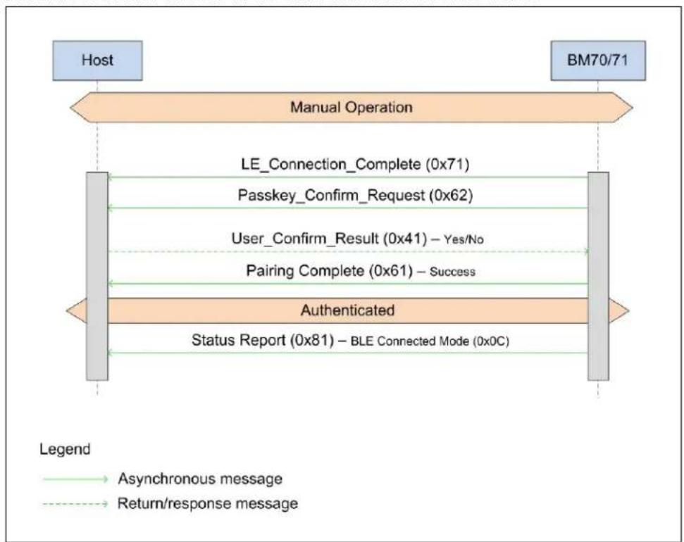
flowchart
sequenceDiagram
    A["Host"] --> B["Manual Operation"]
    B --> C["LE_Connection_Complete (0x71)"]
    B --> D["Passkey_Confirm_Request (0x62)"]
    B --> E["User_Confirm_Result (0x41) – Yes/No"]
    B --> F["Pairing Complete (0x61) – Success"]
    B --> G["Authenticated"]
    G --> H["Status Report (0x81) – BLE Connected Mode (0x0C)"]
    H --> I["Legend"]
    I --> J["Asynchronous message"]
    I --> K["Return/response message"]
Table 1-33 provides the relevant configuration parameters and “Command Set” messages for handling authentication and security in Bluetooth Low Energy.
TABLE 1-33: CONFIGURATION PARAMETERS
| Configuration Operation | Functionality Parameter | Value Command Set Messages | |
| Manual Operation / Auto Operation | Bluetooth Low Energy Features | Data Length Extension = 0x00 – Disabled, 0x01 – EnabledPairing Method = 0x00 – Only legacy pairing enabled [Just Works, Passkey] (pairing method used will be based on I/O capabilities of peer device and BM70/71 module)0x01 – Legacy and LE Secure Connections enabled [Just Works, Passkey, Numeric Comparison] (pairing method used will be based on I/O capabilities of peer device and BM70/71 module)0x02 – Only LE Secure Connections pairing enabled [Numeric Comparison] (pairing success will be based on I/O capabilities and LE Secure Connections being supported in peer device) | N/A, this is all based on I/O capabilities of devices |
| Auto Operation Bluetooth | Low Energy Security Setting | Bluetooth Low Energy Security = 0x00 – Disabled (BM70/71 module informs peer device "pairing not supported", this results in an unauthenticated unencrypted level of security for current connection)0x01 – Pairing Enabled (BM70/71 module will inform peer device, BM70/71 module supports pairing)0x02 – Pairing Enabled, Authentication Required (BM70/71 module informs peer device pairing supported and needs to result in a authenticated encrypted level of security for current connection)Trust Device Connection = 0x00 – Pair, Do not Bond, 0x01 – Pair and BondI/O Capability = 0x00 – Display Only0x01 – Display Yes/No0x02 – Keyboard Only0x03 – No I/O available0x04 – Keyboard and Display | |
| Manual Operation Bluetooth | Low Energy Security Setting | Trust Device Connection = 0x00 – Pair, Do not Bond, 0x01 – Pair and Bond | For Manual Operation OnlyWrite_Paring_Mode_Set-ting(0x0B), controls the I/O capabilities of deviceFor Manual Operation OnlyPairing_Request(0x42) control pair-ing procedure when BM70/71 module is initiatorThe use of the following “Command Set” messages, is based on the role BM70/71 module is playing (initiator or responder)BM70/71 module to host “Command Set” messages:Passkey_Entry_Req(0x60)Pairing_Complete(0x61)Passkey_Confirm_Req(0x62)Host to BM70/71 module “Command Set” messages:Passkey_Entry_Res(0x40)User_Confirm_Res(0x41)Pairing_Request(0x42) |
NOTES:
Chapter 2. Operating Modes, Configuration and Control
This chapter describes the minimum hardware interface required for host control and the protocols used to communicate with the BM70/71 module. There are additional hardware pins on the module, which can be used by the end target application to achieve greater functionality. The protocols described in this document provide information about the direct test, programming, and application commands used for the BM70/71 module.
Note: The remaining communication protocols used for configuring the BM70/71 module are still available to the user, but require additional guidance. Contact a local Microchip representative if design requirements must use those communication protocols.
2.1 HARDWARE INTERFACE
A minimum set of hardware connections is required to interface a host to the BM70/71 module. Figure 2-1 illustrates the minimum connections required by the relevant hardware pins on the module. Making these hardware connections between the host and the BM70/71 module will allow a host to control the behavior of the module.
FIGURE 2-1: BM70/71 MODULE BLOCK DIAGRAM FOR EXTERNAL INTERFACE

2.2 BM70/71 MODE SELECTION
The BM70/71 module's operation or mode is determined by the level of hardware pin P2_0. This pin is sampled when the RST_N pin goes active. The RST_N signal must be active for the minimum time period, so the P2_0 pin logic level is latched into the BM70/71 module. Once the BM70/71 module enters the applicable mode, communication over the UART interface becomes active. The data or protocol used to communicate between the host and the BM70/71 module is based on the mode the module enters after a reset.
At a high level, the test, configuration, and programming modes are entered when the P2_0 pin is latched by the BM70/71 module at logic level "0". The application or run mode, where general Bluetooth Low Energy operation is available, is entered when P2_0 pin is latched by the BM70/71 module at logic level "1". Table 2-1 provides the use of the P2_0 pin.
TABLE 2-1: P2_0 PIN LOGIC LEVEL FUNCTIONALITY
| PIN P2_0 - Logic Level Mode Protocols Enabled | ||
| 0 – Low Direct Test | Configuration Programming | HCI commandConfiguration UpdateMemory Programming |
| 1 – High Application or run | Command Set | |
Table 2-1 represents the three protocols and three modes available when the pin P2_0 is at a logic level of "0". The header value and the data payload of the protocol packet indicates the type of mode/protocol the host put the BM70/71 module into. For more information on protocol descriptions, refer to 2.3 "Command Set Protocol", 2.4 "Configuration Protocol", 2.4.1 "UART Interface Characteristics", and 2.6 "Direct Test Protocol".
Figure 2-2 illustrates the signal level and timing control of the P2_0 pin by a host during a reset event.
FIGURE 2-2: P2_0 PIN IN RESET EVENT

Figure 2-3 illustrates the signal level and timing control of the P2_0 pin during a POR event.
FIGURE 2-3: P2_0 PIN IN POR EVENT

Once a designer implements the necessary signals to allow communication with the end target application's host, the applicable protocols (based on the mode of the BM70/71 module) must be referenced in later sections to learn how to control the behavior of the module.
2.3 COMMAND SET PROTOCOL
When the BM70/71 module enters into Application or Run mode, and Auto Operation or Manual Operation is active (refer to 1.1.2.1 "Auto Operation" and 1.1.2.2 "Manual Operation"), the "Command Set" protocol is used by the host to control the behavior of the BM70/71 module. This protocol loosely follows the Host Command Interface (HCI) logic flow defined in the Bluetooth Low Energy specification. If a user is already familiar with the HCI logic flow, understanding this protocol will be straightforward. This section describes the commands a host uses to command Bluetooth Low Energy operations to occur within the BM70/71 module.
For the purposes of evaluation, Microchip also provides two Graphical User Interface (GUI) based PC programs which implement low-level details (commands and parse the event responses) from the "Command Set" protocol. These PC tools can be used as an aide to understand the information contained in the sub-sections below. The tools are referred to as the Manual Pattern and Auto Pattern tools, and are part of the "Software Tools" that are available for download for the BM70/71 module. The tools are often referred to as "host MCU emulation" tools and are categorized as such in the "Software Tools".
Note: Download the "Software Tools" which are available on the BM70 and BM71 product pages of the Microchip website: www.microchip.com/BM70 for the BM70 EVB and www.microchip.com/BM71 for the BM71 EVB.
2.3.1 General Message Format
Table 2-2 provides the general message format of the “Command Set” protocol between the host and BM70/71 module.
TABLE 2-2: GENERAL MESSAGE FORMAT OF THE COMMAND SET PROTOCOL
| HEAD MID DATA | CRC | ||||
| Start Length | OP | Code Parameter Checksum | |||
| Byte No | 0 | 1 - 2 | 3 | 4 - xx | Length + 3 |
| Size (Byte) | 1 | 2 | 1 | 0 | 1 |
| Value | 0xAA | 1 | Command/Event | Command/Event parameter | Checksum |
| SYNC WORD | Checksum to be calculated | ||||
| TARGET LENGTH | |||||
Checksum rule: Checksum value is the byte value, which yields a result of "0", when added to the summed values of the Length (H), Length (L), OP Code, and Parameter bytes. Table 2-3 provides an example of the checksum value.
TABLE 2-3: EXAMPLE OF THE CHECKSUM VALUE
| Start | Length (H) | Length (L) | OP Code | Parameter | Checksum | |
| Byte No | 0 | 1 | 2 | 3 | 4 | 5 |
| Size (Byte) | 0xAA | 0x00 | 0x02 | 0x01 | 0x00 | 0xFD |
In cases where the checksum calculation fails, the BM70/71 module will send a message back to the host to indicate the checksum failure. For more information on command status, refer to 2.3.3 "Commands and Event Responses".
2.3.2 UART Interface Characteristics
When operating in Application or Run mode, the UART can operate using the following parameters:
• Baud Rate: 2400-921600 bps (configurable)
• Number of data bits: 8
- No parity
- 1 stop bit
- Flow control (configurable in some cases, disabled in all other configurations)
The baud rate is configurable and is set when the BM70/71 module is in configuration mode. Once set, the BM70/71 module will use this baud rate for all "Command Set" protocol communications until changed. UART flow control (RTS/CTS) is available as a configuration parameter only when Auto Operation is selected. Since this protocol is used when Manual Operation is active, the flow control is disabled. For more information, refer to 1.1.2.1 "Auto Operation" and 1.1.2.2 "Manual Operation".
Several other configurable hardware pins can take on different functionality, possibly affecting the timing of communication over the UART. These hardware pins are enabled or disabled based on the requirements of the end target application. For a description of the associated functions in the BM70/71 module, which can affect communication over the UART interface, refer to Section 1.1.2.3 "General Operation".
Table 2-4 provides a list of hardware pin functionality which can affect UART communication.
TABLE 2-4: HARDWARE PIN FUNCTIONALITY FOR UART COMMUNICATION
| Functionality BM70 PINS BM71 PINS | ||
| UART_TX_IND P27 | P27 | |
| UART_RX_IND P00 | (if CTS disabled) | P00 (if CTS disabled) |
| P07 | P12 | |
| P10 | P13 | |
| P11 | P16 | |
| P12 | P17 | |
| P13 | P36 (if RTS disabled) | |
| P22 | ||
| P24 | ||
| P31 | ||
| P32 | ||
| P33 | ||
| P34 | ||
| P35 | ||
| P36 (if RTS disabled) | ||
| WAKEUP P23 | N/A | |
2.3.3 Commands and Event Responses
The command packets are sent by the host to the BM70/71 module over the UART. These packets contain an opcode which determines the sent command, a parameter length field, and parameters for the command. In general, there are three basic types of commands a host can send to the BM70/71 module:
- Configure the BM70/71 module state
- Request a specific action
- Control a connection
The internal logic of the BM70/71 module can be considered a state machine, which has a number of parameters and modes to be configured. Configuration commands can set these parameters/modes while the BM70/71 module is in a specific state. Some commands request a specific action to occur without necessarily altering the state of the BM70/71 module or the state of the connection. When a connection has been created between two peer devices, commands can be sent to manage this connection.
Some messages require certain steps before executing successfully. When this type of message is described, a diagram similar to a sequence diagram will be shown. The diagram will help highlight previous messages which need to be executed so the current message finishes successfully. The commands and events vary in length and inspection of the length field will be performed to get the payload information out of the message. Most commands have a "Command Complete Event" sent by the BM70/71 module to the host when the command completes. Some commands are executed in the background and do not return a "Command Complete Event" when the command finishes. In those cases, the BM70/71 module sends a "Status Report Event" back to the host when it has begun processing the command. When the operation associated with the command has finished, the event which is associated with the command will be sent to the host.
In general, all the messages from the host to the BM70/71 module will have some type of response, but not all messages from the module to the host necessarily require previous input (status message events). These types of messages can be viewed as an internal BM70/71 module status change, synchronized to the occurrence of events outside the scope of the host. The internal logic of the host will be capable of processing these type of messages. The host will wait for the associated response(s) before sending any new messages to the BM70/71 module.
Figure 2-4 illustrates the message sequence diagram at a high level.
FIGURE 2-4:MESSAGE SEQUENCE DIAGRAM
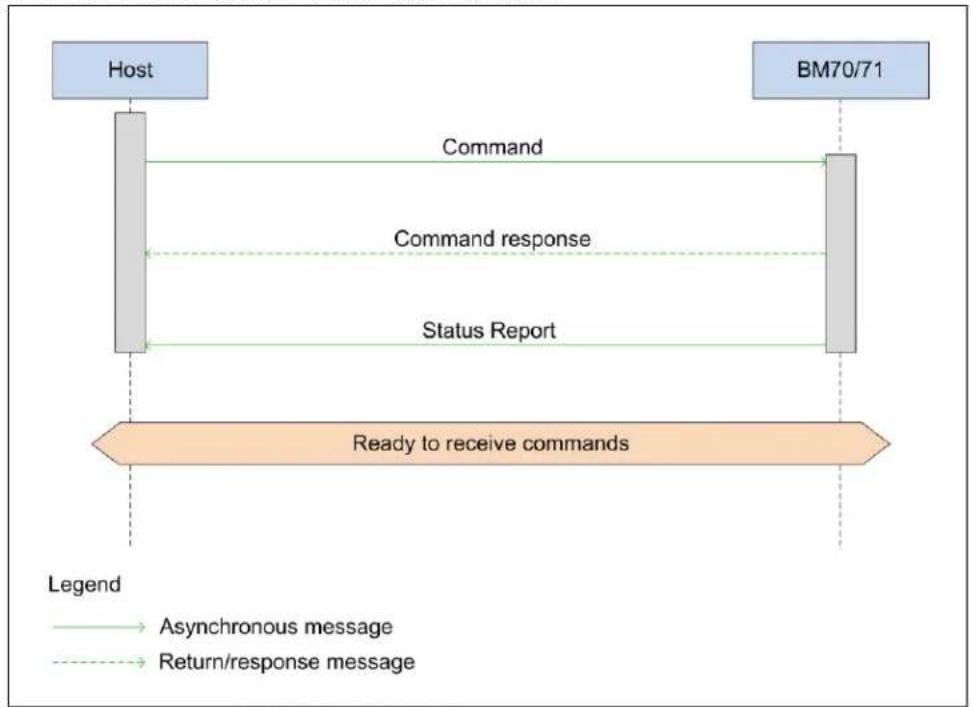
flowchart
graph TD
    A["Host"] -->|Command| B["BM70/71"]
    B -->|Command response| A
    A -->|Status Report| B
    B -->|Ready to receive commands| A
    style A fill:#e6f3ff,stroke:#333
    style B fill:#e6f3ff,stroke:#333
    linkStyle 0 stroke:#000,stroke-width:2px
    linkStyle 1 stroke:#000,stroke-width:2px
    linkStyle 2 stroke:#000,stroke-width:2px
    linkStyle 3 stroke:#000,stroke-width:2px
    linkStyle 4 stroke:#000,stroke-width:2px
    linkStyle 5 stroke:#000,stroke-width:2px
    linkStyle 6 stroke:#000,stroke-width:2px
    linkStyle 7 stroke:#000,stroke-width:2px
    linkStyle 8 stroke:#000,stroke-width:2px
    linkStyle 9 stroke:#000,stroke-width:2px
    linkStyle 10 stroke:#000,stroke-width:2px
    linkStyle 11 stroke:#000,stroke-width:2px
    linkStyle 12 stroke:#000,stroke-width:2px
    linkStyle 13 stroke:#000,stroke-width:2px
    linkStyle 14 stroke:#000,stroke-width:2px
    linkStyle 15 stroke:#000,stroke-width:2px
    linkStyle 16 stroke:#000,stroke-width:2px
    linkStyle 17 stroke:#000,stroke-width:2px
    linkStyle 18 stroke:#000,stroke-width:2px
    linkStyle 19 stroke:#000,stroke-width:2px
    linkStyle 20 stroke:#000,stroke-width:2px
    linkStyle 21 stroke:#000,stroke-width:2px
    linkStyle 22 stroke:#000,stroke-width:2px
    linkStyle 23 stroke:#000,stroke-width:2px
    linkStyle 24 stroke:#000,stroke-width:2px
    linkStyle 25 stroke:#000,stroke-width:2px
    linkStyle 26 stroke:#000,stroke-width:2px
    linkStyle 27 stroke:#000,stroke-width:2px
    linkStyle 28 stroke:#000,stroke-width:2px
    linkStyle 29 stroke:#000,stroke-width:2px
    linkStyle 30 stroke:#000,stroke-width:2px
    linkStyle 31 stroke:#000,stroke-width:2px
    linkStyle 32 stroke:#000,stroke-width:2px
    linkStyle 33 stroke:#000,stroke-width:2px
    linkStyle 34 stroke:#000,stroke-width:2px
    linkStyle 35 stroke:#000,stroke-width:2px
    linkStyle 36 stroke:#000,stroke-width:2px
    linkStyle 37 stroke:#000,stroke-width:2px
    linkStyle 38 stroke:#000,stroke-width:2px
    linkStyle 39 stroke:#000,stroke-width:2px
    linkStyle 40 stroke:#000,stroke-width:2px
    linkStyle 41 stroke:#000,stroke-width:2px
    linkStyle 42 stroke:#000,stroke-width:2px
    linkStyle 43 stroke:#000,stroke-width:2px
    linkStyle 44 stroke:#000,stroke-width:2px
    linkStyle 45 stroke:#000,stroke-width:2px
    linkStyle 46 stroke:#e6f3ff,stroke-width:1px
    linkStyle 47 stroke:#e6f3ff,stroke-width:1px
    linkStyle 48 stroke:#e6f3ff,stroke-width:1px
    linkStyle 49 stroke:#e6f3ff,stroke-width:1px
    linkStyle 50 stroke:#e6f3ff,stroke-width:1px
When the host is waiting for a response, implement the timeout logic in case of errant operation of the BM70/71 module. This timeout logic period can vary based on the types of messages the host sends to the BM70/71 module. For commands which include RF communication (for example, the GAP Create Connection command), the time to execute the command will depend on the RF traffic and/or command parameters. Therefore, the response from the BM70/71 module back to the host will be delayed, impacting any timeout period logic. Guidelines for a host implementing timeout logic to guard against errant BM70/71 module communication are:
- For commands without direct RF communication: 2 seconds timeout period
- For commands with direct RF communication included: a timeout period is NOT suggested
2.3.3.1 READ LOCAL INFORMATION (OPCODE - 0X01)
This command is sent from the host to the BM70/71 module to retrieve:
- The internal firmware version of the module in Binary Coded Decimal (BCD) format
• The Bluetooth address of the BM70/71 module - The silicon chip Identification (only firmware version 106 and above).
In most cases this information is useful to the host for version control and to gain manufacturing information. This command can also be used as a fast way of detecting if the BM70/71 module is up and running.
2.3.3.1.1 Command Format, Host to BM70/71 Module
Table 2-5 provides the details of the command format from the host to the BM70/71 module.
TABLE 2-5: COMMAND FORMAT, HOST TO BM70/71 MODULE
| Start Length (L) Length (H) OP Code Checksum | |||||
| Byte No | 0 | 1 | 2 | 3 | 5 |
| Value | 0xAA | 0x00 | 0x01 | 0x01 | value |
2.3.3.1.2 Defaults
This does not apply to this command.
2.3.3.1.3 Example
Figure 2-5 illustrates an example of the Read Local Information(0x01) command sent from the host to the BM70/71 module.
FIGURE 2-5: SEQUENCE DIAGRAM OF READ LOCAL INFORMATION
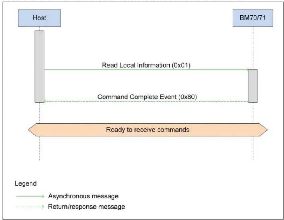
flowchart
graph TD
    A["Host"] -->|Read Local Information (0x01)| B["BM70/71"]
    B -->|Command Complete Event (0x80)| A
    A -->|Ready to receive commands| C["End"]
    style A fill:#e6f3ff,stroke:#333
    style B fill:#e6f3ff,stroke:#333
    style C fill:#e6f3ff,stroke:#333
2.3.3.1.4 Response Format, BM70/71 to Host
The BM70/71 module will respond to this command with a Command Complete Event (0x80) response and will add additional data to the parameter field of the event message. The length of this message changes based on the firmware version of the device. BM70/71 modules with firmware version 106 or later will respond with the silicon identification value in the message. BM70/71 modules with firmware version 105 or earlier will be included in the silicon identification value. The parameter field and variables are based on the firmware version, silicon chip identification, and the programmed Bluetooth address.
Table 2-6 provides the details of the response format, from the BM70/71 module to the host.
TABLE 2-6: RESPONSE FORMAT, BM70/71 MODULE TO HOST
| Start Length (H) Length (L) Parameter Checksum | |||||
| Byte No 0 1 2 | 3 to n | n+4 | |||
| Value | 0xAA | 0x00 | 0x0D or 0x0E | see Table2-7 | value |
Table 2-7 provides the details of the parameter values and lengths.
TABLE 2-7: PARAMETER VALUES AND LENGTHS
| Value of Parameter | Parameter Description | Length |
| Value of Parameter (3) | ||
| 0x80 | Command succeeded | 1 byte |
| Value of Parameter (4) | ||
| 0x01 | Opcode which was processed by BM70/71 module | 1 byte |
| Value of Parameter (5) | ||
| 0xXX | Command completion status (See Table 2-119) | 1 byte |
| Value of Parameter (6 to 9) | ||
| 0xXXXX_XXXX | Firmware version encoded as BCD | 4 bytes |
| Value of Parameter (10 to 15) | ||
| 0xXXXX_XXXX_XXXX | Bluetooth address | 6 bytes |
| Value of Parameter (16) | ||
| 0x00 | BM70 | Silicon Identification field only applies with firmware version 106 or above |
| 0x01 | BM71 | |
| 0x02 | IS1870 | |
| 0x03 | IS1871 | |
2.3.3.1.5 Applicable Configuration
This command is available in both Manual Operation and Auto Operation configuration. In Auto Operation configuration, there is a time period around when this command can be sent by the host. If the time period has expired in Auto Operation configuration, this command will be ignored.
2.3.3.2 RESET (OPCODE - 0X02)
This command performs a reset on the BM70/71 module. When this command is issued, the behavior of the BM70/71 module is same as when the hardware RST_N pin is used. Internally this command returns the BM70/71 module to "Idle mode" in the Standby state, which is indicated in the response.
This command is typically used when the RST_N pin is not available to the host to correct any errant operation or to synchronize the host with the BM70/71 module.
2.3.3.2.1 Command Format, Host to BM70/71 Module
Table 2-8 provides the details of the command format, from the host to the BM70/71 module.
TABLE 2-8: COMMAND FORMAT, HOST TO BM70/71 MODULE
| Start Length (H) Length (L) OP Code Checksum | |||||
| Byte No | 0 | 1 | 2 | 3 | 5 |
| Value | 0xAA | 0x00 | 0x01 | 0x02 | value |
2.3.3.2.2 Defaults
This does not apply to this command.
2.3.3.2.3 Example
Figure 2-6 illustrates an example of the reset command sent from the host to the BM70/71 module.
FIGURE 2-6: SEQUENCE DIAGRAM OF RESET

flowchart
graph LR
    A["Host"] --> B["Reset (0x02)"]
    B --> C["Status Report Event (0x81)"]
    C --> D["Ready to receive commands"]
    D --> E["Return/response message"]
    style A fill:#e6f3ff,stroke:#333
    style B fill:#e6f3ff,stroke:#333
    style C fill:#e6f3ff,stroke:#333
    style D fill:#e6f3ff,stroke:#333
    style E fill:#e6f3ff,stroke:#333
2.3.3.2.4 Response Format, BM70/71 Module to Host
The BM70/71 module will respond to this command with a Status Report Event (0x81) response. The value in the status will indicate that the BM70/71 module has returned to "Idle mode". For more information on the response format, refer to 2.3.3.52 "Status Report Event (opcode - 0x81)".
2.3.3.2.5 Applicable configuration
This command is only available in Manual Operation.
2.3.3.3 READ BM70/71 STATUS (OPCODE - 0X03)
This command is used to read the internal status of the BM70/71 module. This command cannot be used in the Shutdown state because the BM70/71 module is inactive.
2.3.3.3.1 Command Format, Host to BM70/71 Module
Table 2-9 provides the details of the command format from the host to the BM70/71 module.
TABLE 2-9: COMMAND FORMAT, HOST TO BM70/71 MODULE
| Start Length (H) Length (L) OP Code Checksum | |||||
| Byte No | 0 | 1 | 2 | 3 | 5 |
| Value | 0xAA | 0x00 | 0x01 | 0x03 | value |
2.3.3.3.2 Defaults
This does not apply to this command.
2.3.3.3.3 Example
Figure 2-7 illustrates an example of the Read BM70/71 Status(0x03) command sent from the host to the BM70/71 module.
FIGURE 2-7: SEQUENCE DIAGRAM OF READ BM70/71 STATUS

flowchart
graph TD
    A["Host"] --> B["Read BM70/71 Status (0x03)"]
    B --> C["Status Report Event (0x81)"]
    C --> D["Ready to receive commands"]
    D --> E["Return/response message"]
    style A fill:#e6f7ff,stroke:#333
    style B fill:#e6f7ff,stroke:#333
    style C fill:#e6f7ff,stroke:#333
    style D fill:#e6f7ff,stroke:#333
    style E fill:#e6f7ff,stroke:#333
2.3.3.3.4 Response Format, BM70/71 Module to Host
The BM70/71 module will respond to this command with a Status Report Event (0x81) response. The value in the status will indicate the mode (temporary sub-state) of the BM70/71 module. The BM70/71 module has a total of nine modes. All modes do not apply to all states within the BM70/71 module.
Table 2-10 provides the details of the response format from the BM70/71 module to the host.
TABLE 2-10: RESPONSE FORMAT, BM70/71 MODULE TO HOST
| Start Length (H) | Length (L) | OP Code | Parameter | Checksum | ||
| Byte No | 0 | 1 | 2 | 3 | 4 | 5 |
| Value | 0xAA | 0x00 | 0x02 | 0x81 | see Table 2-121 | value |
2.3.3.3.5 Applicable Configuration
This command is available in Manual Operation and Auto Operation only when the "Configuration Window" is active (refer to 1.1.2.1.3 "Auto Operation – Configuration Timeout").
2.3.3.4 READ BM70/71 ADC VALUE (OPCODE - 0X04)
This command is used to read the voltage present on the applicable analog pin/channel. The pin has to be configured appropriately, and some of the channel numbers in the command do not apply to the BM70/71 module because the pin is not available (see 1.1.2.2.2 "Manual Operation – Analog Pins"). All channel numbers are shown for the purpose of developers using the IS1870/71 chip directly.
2.3.3.4.1 Command Format, Host to BM70/71 Module
Table 2-11 provides details of the command format from the host to the BM70/71 module.
TABLE 2-11: COMMAND FORMAT, HOST TO BM70/71 MODULE
| Start Length (H) | Length (L) | OP Code | Parameter | Checksum | ||
| Byte No 0 1 | 2 | 3 | 4 | 5 | ||
| Value | 0xAA | 0x00 | 0x02 | 0x04 | see Table 2-12 | value |
Table2-12 provides the parameter values and lengths.
TABLE 2-12: PARAMETER VALUES AND LENGTHS
| Value of Parameter (4) | Parameter Description | Length |
| 0x00 | Channel 0 | 1 byte |
| 0x01 | Channel 1 | |
| 0x02 | Channel 2 | |
| 0x03 | Channel 3 | |
| 0x04 | Channel 4 | |
| 0x05 | Channel 5 | |
| 0x06 | Channel 6 | |
| 0x07 | Channel 7 | |
| 0x08 | Channel 8 | |
| 0x09 | Channel 9 | |
| 0x0A | Channel 10 | |
| 0x0B | Channel 11 | |
| 0x0C | Channel 12 | |
| 0x0D | Channel 13 | |
| 0x0E | Channel 14 | |
| 0x0F | Channel 15 | |
| 0x10 | Battery Voltage | |
| 0x11 | Temperature Value |
2.3.3.4.2 Defaults
This does not apply to this command.
2.3.3.4.3 Example
Figure 2-8 illustrates an example of reading the ADC value from the host to the BM70/71 module.
FIGURE 2-8: SEQUENCE DIAGRAM OF READ BM70/71 ADC VALUE

flowchart
graph LR
    A["Host"] --> B["Read ADC Channel (0x04)"]
    B --> C["Command Complete Event (0x80)"]
    C --> D["Ready to receive commands"]
    D --> E["Return/response message"]
    style A fill:#e6f3ff,stroke:#333
    style B fill:#e6f3ff,stroke:#333
    style C fill:#e6f3ff,stroke:#333
    style D fill:#e6f3ff,stroke:#333
    style E fill:#e6f3ff,stroke:#333
2.3.3.4.4 Response Format, BM70/71 Module to Host
The BM70/71 module will respond to this command with a Command Complete Event (0x80) response. The values returned indicate if the command is successful or not. If the command is successful, the values for the measured voltage and resolution (step size) will follow. The step size is based on an internal formula that the host cannot control (for more information, refer to 1.1.2.2.2 "Manual Operation – Analog Pins").
Table 2-13 provides details of the response format from the BM70/71 module to the host.
TABLE 2-13: RESPONSE FORMAT, BM70/71 MODULE TO HOST
| Start Length (H) Length (L) OP Code Parameter Checksum | ||||||
| Byte No | 0 | 1 | 2 | 3 | 4 to 7 | 5 |
| Value | 0xAA | 0x00 | 0x02 | 0x82 | see Table 2-14 | value |
Table 2-14 provides parameter values and lengths.
TABLE 2-14: PARAMETER VALUES AND LENGTHS
| Value of Parameter Parameter | Parameter Description Length | |
| Value of Parameter (4) | ||
| 0x00 0x00 – command successful 1 byte | ||
| 0x01 0x01-0xFF, command failure (for table of values, refer to Table 2-119) | ||
| Value of Parameter (5) | ||
| 0x00 Step size | 0x00 – no step size, raw ADC Value0x01 – 0.1V0x02 – 0.05V0x03 – 0.025V | 1 byte |
| Value of Parameter (6 to 7) | ||
| 0xXXXX Digital value from Analog to Digital conversionParameter 6 is Most Significant Byte (MSB)Parameter 7 is Least Significant Byte (LSB) | 2 bytes | |
2.3.3.4.5 Applicable Configuration
This command is only available in Manual Operation.
2.3.3.5 INTO SHUTDOWN MODE (OPCODE - 0X05)
This command is sent from the host to the BM70/71 module to put the BM70/71 module into Shutdown mode. This will put the BM70/71 module into the "Deep-sleep/Shutdown" low-power mode, which is the lowest current consumption mode for the BM70/71 module. The BM70/71 module must be in "Idle mode" for this command to be successful.
2.3.3.5.1 Command Format, Host to BM70/71 Module
Table 2-15 provides details of the command format from the host to the BM70/71 module.
TABLE 2-15: COMMAND FORMAT, HOST TO BM70/71 MODULE
| Start Length (H) Length (L) OP Code Checksum | |||||
| Byte No | 0 | 1 | 2 | 3 | 5 |
| Value | 0xAA | 0x00 | 0x01 | 0x05 | value |
2.3.3.5.2 Defaults
This does not apply to this command.
2.3.3.5.3 Example
Figure 2-9 illustrates an example of the Into Shutdown(0x05) command from the host to the BM70/71 module.
FIGURE 2-9: SEQUENCE DIAGRAM OF INTO SHUTDOWN MODE

flowchart
graph TD
    A["Host"] -->|Into Shutdown (0x05)| B["BM70/71"]
    B -->|Command Complete Event (0x80)| A
    A -->|Status Report Event (0x81)| B
    B -->|Cannot receive commands, need wake-up| A
    style A fill:#e6f3ff,stroke:#333
    style B fill:#e6f3ff,stroke:#333
2.3.3.5.4 Response Format, BM70/71 Module to Host
The BM70/71 module will respond with two replies to the host when receiving the Shutdown command. The BM70/71 module will send a Command Complete Event (0x80) response on successfully receiving the message and processing it. The BM70/71 module will then send a Status Report Event(0x81) response when the command has fully completed and the BM70/71 module is entering the Shutdown state. If the Into Shutdown(0x05) command is incorrectly processed or cannot be completed, the Status Report Event(0x81) response will never be sent and the Command Complete Event(0x80) response will contain an error code for the host to process.
Table 2-16 provides the details of the Command Complete Event(0x80) response format from the BM70/71 module to the host.
TABLE 2-16: RESPONSE FORMAT, BM70/71 MODULE TO HOST
| Start Length (H) | Length (L) | OP Code | Parameter | Checksum | ||
| Byte No | 0 | 1 | 2 | 3 | 4 to 7 | 5 |
| Value | 0xAA | 0x00 | 0x02 | 0x80 | see Table 2-17 | value |
Table 2-17 provides the parameter values and lengths.
TABLE 2-17: PARAMETER VALUES AND LENGTHS
| Value of Parameter (4) | Parameter Description | Length |
| 0x00 | 0x00 – command successful | 1 byte |
| 0x01 | 0x01 – 0xFF, command failure (for table of values, refer to Table 2-119) |
Table 2-18 provides details of the Status Report Event(0x81) response format from the BM70/71 module to the host.
TABLE 2-18: STATUS REPORT RESPONSE FORMAT
| Start | Length (H) | Length (L) | OP Code | Parameter Checksum | ||
| Byte No | 0 | 1 | 2 | 3 | 4 to 7 | 5 |
| Value | 0xAA | 0x00 | 0x02 | 0x81 | see Table 2-121 | value |
2.3.3.5.5 Applicable Configuration
This command is only available in Manual Operation.
2.3.3.6 READ DEVICE NAME (OPCODE - 0X07)
This command is used by the host to read the device name fragment in the BM70/71. During configuration this value can be programmed by the host or by using the Write Device Name(0x08) command.
2.3.3.6.1 Command Format, Host to BM70/71 Module
Table 2-19 provides details of the command format from the host to the BM70/71 module.
TABLE 2-19: COMMAND FORMAT, HOST TO BM70/71 MODULE
| Start Length (H) Length (L) OP Code Checksum | |||||
| Byte No | 0 | 1 | 2 | 3 | 5 |
| Value | 0xAA | 0x00 | 0x01 | 0x07 | value |
2.3.3.6.2 Defaults
This does not apply to this command.
2.3.3.6.3 Example
Figure 2-10 illustrates an example of the Read Device Name(0x07) command sent from the host to the BM70/71 module.
FIGURE 2-10: SEQUENCE DIAGRAM OF READ DEVICE NAME
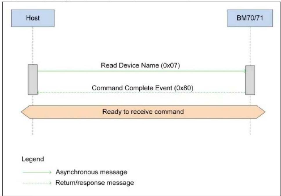
flowchart
graph LR
    A["Host"] -->|Read Device Name (0x07)| B["BM70/71"]
    B -->|Command Complete Event (0x80)| A
    A <-->|Ready to receive command| B
    style A fill:#e6f3ff,stroke:#333
    style B fill:#e6f3ff,stroke:#333
    note right of A: Legend
        Green solid arrow: Asynchronous message
        Blue dashed arrow: Return/response message
2.3.3.6.4 Response Format, BM70/71 Module to Host
The BM70/71 replies to the host with the Command Complete Event(0x80) response, with the device name added to the parameter field of this event message. The device name is limited to the length allowed in Configuration mode.
Table 2-20 provides details of the Command Complete Event(0x80) response format from the BM70/71 module to the host.
TABLE 2-20: RESPONSE FORMAT, BM70/71 MODULE TO HOST
| Start Length (H) Length (L) OP Code Parameter Checksum | ||||||
| Byte No 0 1 2 | 3 | 4 to n | 5 | |||
| Value | 0xAA | 0x00 | 0xXX | 0x80 | see Table 2-21 | value |
Table 2-21 provides the parameter values and lengths.
TABLE 2-21: PARAMETER VALUES AND LENGTHS
| Value of Parameter | Parameter Description | Length |
| Value of Parameter (4) | ||
| 0xXX | 0x00 – command successful | 1 byte |
| 0x01 – 0xFF, command failure (for table of values, refer to Table 2-119) | ||
| Value of Parameter (5 to n) | ||
| 0xXX | This will be the ASCII hex values of the string programmed into the name fragment field | Length = (n+1) - 5 bytes |
2.3.3.6.5 Applicable Configuration
This command is only available in Manual Operation.
2.3.3.7 WRITE DEVICE NAME (OPCODE - 0X08)
This command is used to assign a name to the BM70/71 module. This name will be seen by remote devices performing a scan. This command can only be sent from "Idle mode" while in the Standby state.
2.3.3.7.1 Command Format, Host to BM70/71 Module
Table 2-22 provides details of the command format from the host to the BM70/71 module.
TABLE 2-22: COMMAND FORMAT, HOST TO BM70/71 MODULE
| Start Length (H) Length (L) OP Code Parameter Checksum | ||||||
| Byte No | 0 | 1 | 2 | 3 | 4 to n | 5 |
| Value | 0xAA | 0x00 | 0xXX | 0x08 | see Table 2-23 | value |
Table 2-21 provides the parameter values and lengths.
TABLE 2-23: PARAMETERS VALUES AND LENGTHS
| Value of Parameter | Parameter Description | Length |
| Value of Parameter (4) | ||
| 0x00 | 0x00 – Reserved | 1 byte |
| Value of Parameter (5 to n) | ||
| 0xXX | Device Name in ASCII hex values | Length = (n+1) - 5 bytes |
2.3.3.7.2 Defaults
This does not apply to this command.
2.3.3.7.3 Example
Figure 2-11 illustrates an example of the Write Device Name(0x08) command sent from the host to the BM70/71 module.
FIGURE 2-11: SEQUENCE DIAGRAM OF WRITE DEVICE NAME

flowchart
graph TD
    A["Host"] -->|Write Device Name (0x08)| B["BM70/71"]
    B -->|Command Complete Event (0x80)| A
    A -->|Ready to receive command| C["End"]
    style A fill:#e6f3ff,stroke:#333
    style B fill:#e6f3ff,stroke:#333
    style C fill:#e6f3ff,stroke:#333
2.3.3.7.4 Response Format, BM70/71 Module to Host
The BM70/71 module returns the Command Complete Event(0x80) response and does not append additional data to the event response. For more information, refer to 2.3.3.51 "Command Complete Event (opcode - 0x80)".
2.3.3.7.5 Applicable Configuration
This command is only available in Manual Operation.
2.3.3.8 ERASE ALL PAIRED BONDED DEVICE INFORMATION (OPCODE - 0x09)
This command is used to erase all saved Long Term Keys (LTK) from the pairing process. This list of keys is a list of the remote devices the BM70/71 module has bonded with. This command can only be sent while the BM70/71 module is in "Idle mode" or the "Configuration Window" is active while in the Standby state.
2.3.3.8.1 Command Format, Host to BM70/71 Module
Table 2-24 provides details of the command format from the host to the BM70/71 module.
TABLE 2-24: COMMAND FORMAT, HOST TO BM70/71 MODULE
| Start Length (H) Length (L) OP Code Checksum | |||||
| Byte No | 0 | 1 | 2 | 3 | 5 |
| Value | 0xAA | 0x00 | 0x01 | 0x09 | value |
2.3.3.8.2 Defaults
This does not apply to this command.
2.3.3.8.3 Example
Figure 2-12 illustrates an example of the Erase All Paired Bonded Device Information (0x09) command sent from the host to the BM70/71 module.
FIGURE 2-12: SEQUENCE DIAGRAM OF ERASE PAIRED_BONDED DEVICE
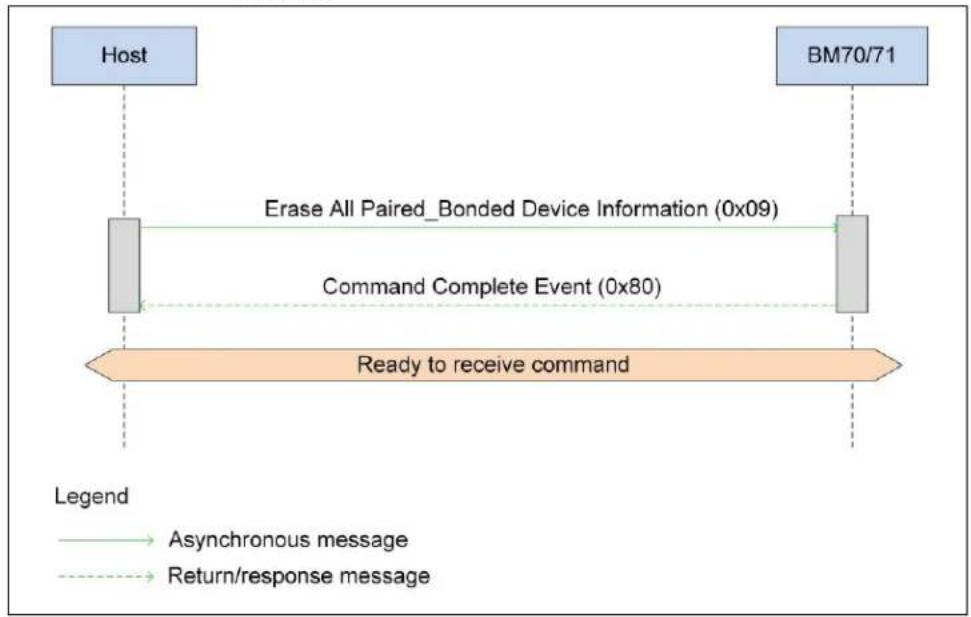
flowchart
graph TD
    A["Host"] -->|Erase All Paired_Bonded Device Information (0x09)| B["BM70/71"]
    B -->|Command Complete Event (0x80)| A
    A -->|Ready to receive command| B
    style A fill:#e6f3ff,stroke:#333
    style B fill:#e6f3ff,stroke:#333
2.3.3.8.4 Response Format, BM70/71 Module to Host
The BM70/71 module returns the Command Complete Event (0x80) response and does not append additional data to the event response. For more information, refer to 2.3.3.51 "Command Complete Event (opcode - 0x80)".
2.3.3.8.5 Applicable Configuration
This command applies to Manual Operation and Auto Operation only when the "Configuration Window" is active.
2.3.3.9 READ PAIRING MODE SETTING (OPCODE - 0X0A)
This command is used by the host to find out the settings of the current I/O capabilities of the BM70/71 module. The value returned has an overall impact on the level of security achieved when the pairing process is complete (refer to 1.1.2.3.6 "General Operation - Security").
2.3.3.9.1 Command Format, Host to BM70/71 Module
Table 2-25 provides details of the command format from the host to the BM70/71 module.
TABLE 2-25: COMMAND FORMAT, HOST TO BM70/71 MODULE
| Start Length (H) Length (L) OP Code Checksum | |||||
| Byte No 0 1 | 2 | 3 | 5 | ||
| Value | 0xAA | 0x00 | 0x01 | 0x0A | value |
2.3.3.9.2 Defaults
This does not apply to this command.
2.3.3.9.3 Example
Figure 2-13 illustrates an example of the Read Pairing Mode Setting(0x0A) command from the host to the BM70/71 module.
FIGURE 2-13: SEQUENCE DIAGRAM OF READ PAIRING MODE
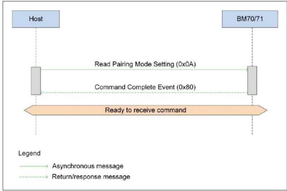
flowchart
graph TD
    A["Host"] --> B["Read Pairing Mode Setting (0x0A)"]
    B --> C["Command Complete Event (0x80)"]
    C --> D["Ready to receive command"]
    D --> E["BM70/71"]
    style A fill:#e6f3ff,stroke:#333
    style E fill:#e6f3ff,stroke:#333
2.3.3.9.4 Response Format, BM70/71 Module to Host
The BM70/71 module returns the Command Complete Event(0x80) response with the value of the current I/O capability added in the parameters field of this event message.
Table 2-26 provides details of the Command Complete Event(0x80) response format from the BM70/71 module to the host.
TABLE 2-26: RESPONSE FORMAT, BM70/71 MODULE TO HOST
| Start Length (H) Length (L) OP Code Parameter Checksum | ||||||
| Byte No | 0 | 1 | 2 | 3 | 4 to 5 | 5 |
| Value | 0xAA | 0x00 | 0x02 | 0x80 | see Table 2-27 | value |
Table 2-27 provides the parameter values and lengths.
TABLE 2-27: PARAMETERS VALUES AND LENGTHS
| Value of Parameter | Parameter Description | Length |
| Value of Parameter (4) | ||
| 0xXX | 0x00 – command successful | 1 byte |
| 0x01 – 0xFF, command failure (for table of values, refer to Table 2-119) | ||
| Value of Parameter (5) | ||
| 0x00 | Display Only | 1 byte |
| 0x01 | Display Yes/No | |
| 0x02 | Keyboard Only | |
| 0x03 | No I/O Capabilities | |
| 0x04 | Keyboard + Display | |
2.3.3.9.5 Applicable configuration
This command applies to Manual Operation and Auto Operation only when the "Configuration Window" is active.
2.3.3.10 WRITE PAIRING MODE SETTING (OPCODE - 0X0B)
This command is used to write the I/O capability of the host into the BM70/71 module. The written value has an overall impact on the level of security the connection will have after the pairing process is completed (refer to 1.1.2.3.6 "General Operation - Security").
2.3.3.10.1 Command Format, Host to BM70/71 Module
Table 2-28 provides details of the command format from the host to the BM70/71 module.
TABLE 2-28: COMMAND FORMAT, HOST TO BM70/71 MODULE
| Start Length (H) Length (L) OP Code Parameter Checksum | ||||||
| Byte No | 0 | 1 | 2 | 3 | 4 to 5 | 5 |
| Value | 0xAA | 0x00 | 0x01 | 0x0B | see Table 2-29 | value |
Table 2-29 provides the parameter values and lengths.
TABLE 2-29: PARAMETERS VALUES AND LENGTHS
| Value of Parameter | Parameter Description | Length |
| Value of Parameter (4) | ||
| 0x00 | 0x00 – Reserved, write as 0x00 | 1 byte |
| Value of Parameter (5) | ||
| 0x00 | Display Only | 1 byte |
| 0x01 | Display Yes/No | |
| 0x02 | Keyboard Only | |
| 0x03 | No I/O Capabilities | |
| 0x04 | Keyboard + Display | |
2.3.3.10.2 Defaults
This does not apply to this command.
2.3.3.10.3 Example
Figure 2-14 illustrates an example of the Write Pairing Mode Setting (0x0B) command from the host to the BM70/71 module.
FIGURE 2-14: SEQUENCE DIAGRAM OF WRITE PAIRING MODE

flowchart
graph TD
    A["Host"] --> B["Read Pairing Mode Setting (0x0B)"]
    B --> C["Command Complete Event (0x80)"]
    C --> D["Ready to receive command"]
    D --> E["Return/response message"]
    style A fill:#e6f3ff,stroke:#333
    style B fill:#e6f3ff,stroke:#333
    style C fill:#e6f3ff,stroke:#333
    style D fill:#e6f3ff,stroke:#333
    style E fill:#e6f3ff,stroke:#333
2.3.3.10.4 Response Format, BM70/71 Module to Host
The BM70/71 module returns the Command Complete Event(0x80) response and does not append additional data to the event response. For more information on the format of the response, refer to 2.3.3.51 "Command Complete Event (opcode - 0x80)".
2.3.3.10.5 Applicable Configuration
This command applies to Manual Operation when the BM70/71 module is in "Idle mode" in the Standby state, and only to Auto Operation when the "Configuration Window" is active.
2.3.3.11 READ ALL PAIRED BONDED DEVICE INFORMATION (OPCODE - 0X0C)
This command is used to read the bonded (part of the pairing process) device list of the BM70/71 module. The BM70/71 module can only store up to the last eight devices that have bonded. When bonding occurs, the LTK is exchanged and saved.
2.3.3.11.1 Command Format, Host to BM70/71 Module
Table 2-30 provides details of the command format from the host to the BM70/71 module.
TABLE 2-30: COMMAND FORMAT, HOST TO BM70/71 MODULE
| Start Length (H) Length (L) OP Code Checksum | |||||
| Byte No 0 1 | 2 | 3 | 5 | ||
| Value | 0xAA | 0x00 | 0x01 | 0x0C | value |
2.3.3.11.2 Defaults
This does not apply to this command.
2.3.3.11.3 Example
Figure 2-15 illustrates an example of reading the paired and bonded device list from the host to the BM70/71 module.
FIGURE 2-15: SEQUENCE DIAGRAM OF READ PAIRED_BONDED DEVICE

flowchart
graph LR
    A["Host"] --> B["Read Pairing Mode Setting (0x0C)"]
    B --> C["Command Complete Event (0x80)"]
    C --> D["Ready to receive command"]
    D --> E["BM70/71"]
    style A fill:#e6f3ff,stroke:#333
    style E fill:#e6f3ff,stroke:#333
2.3.3.11.4 Response Format, BM70/71 Module to Host
The BM70/71 module returns the Command Complete Event(0x80) response with the pairing and bonding list added to the parameters field of the event message. The total length is dependent on how many devices the BM70/71 module has stored.
Table 2-31 provides details of the Command Complete Event(0x80) response format from the BM70/71 module to the host.
TABLE 2-31: RESPONSE FORMAT, BM70/71 MODULE TO HOST
| Start Length (H) Length (L) OP Code Parameter Checksum | ||||||
| Byte No | 0 | 1 | 2 | 3 | 4 to n | 5 |
| Value | 0xAA | 0x00 | 0x0C-0x43 | 0x80 | see Table 2-32 | value |
Table 2-32 provides the parameter values and lengths.
TABLE 2-32: PARAMETER VALUES AND LENGTHS
| Value of Parameter | Parameter Description | Length |
| Value of Parameter (4) | ||
| 0x00 | 0x00 – command successful | 1 byte |
| 0x01 | 0x01 – 0xFF, command failure (for table of values, refer to Table 2-119) | |
| Value of Parameter (5) | ||
| 0x00 | 0xXX, number of paired and bonded devices. Up to 8 (max) | 1 byte |
| Value of Parameter (n to (n+7)) | ||
| 0xXX | Paired device index (0 to 7) | 8 bytes |
| 0xXX | Link Priority0x01 - Most recent device•••0x08 - Oldest device | |
| 0xXX XX XX XX XX XX | Paired and Bonded device Bluetooth address | |
2.3.3.11.5 Applicable Configuration
This command can be used in Manual Operation when the BM70/71 module is in "Idle mode" in the Standby state, and in Auto Operation only when the "Configuration Window" is active.
2.3.3.12 DELETE PAIRED BONDED DEVICE (OPCODE - 0X0D)
This command is sent by the host to delete a particular device from the bonded list. The device is identified using an index value, similar to an index used to address a particular array element in "C" code. For information on device index references, refer to the 2.3.3.11 "Read All Paired_Bonded Device Information (opcode - 0x0C)" command.
2.3.3.12.1 Command Format, Host to BM70/71 Module
Table 2-33 provides details of the command format from the host to the BM70/71 module.
TABLE 2-33: COMMAND FORMAT, HOST TO BM70/71 MODULE
| Start Length (H) Length (L) OP Code Parameter Checksum | ||||||
| Byte No | 0 | 1 | 2 | 3 | 4 | 5 |
| Value | 0xAA | 0x00 | 0x03 | 0x0D | see Table 2-34 | value |
Table 2-34 provides the parameter values and lengths.
TABLE 2-34: PARAMETER VALUES AND LENGTHS
| Value of Parameter | Parameter Description | Length |
| 0x00 | Device IndexThe range of the device index is:0x00•••0x07 | 1 byte |
2.3.3.12.2 Defaults
This does not apply to this command.
2.3.3.12.3 Example
Figure 2-16 illustrates an example of deleting the paired and bonded device from the host to the BM70/71 module.
FIGURE 2-16: SEQUENCE DIAGRAM OF DELETE PAIRED_BONDED DEVICE
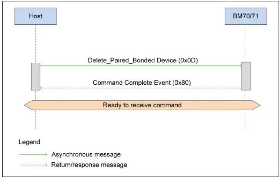
flowchart
graph TD
    A["Host"] --> B["Delete_Paired_Bonded Device (0x0D)"]
    B --> C["Command Complete Event (0x80)"]
    C --> D["Ready to receive command"]
    D --> E["Return/response message"]
    style A fill:#cce5ff,stroke:#333
    style B fill:#e6f3ff,stroke:#333
    style C fill:#e6f3ff,stroke:#333
    style D fill:#ffe6cc,stroke:#333
    style E fill:#fff2cc,stroke:#333
2.3.3.12.4 Response Format, BM70/71 Module to Host
The BM70/71 module returns the Command Complete Event(0x80) response and does not append additional data to the event message. For more information on the format of the response, refer to 2.3.3.51 "Command Complete Event (opcode - 0x80)".
2.3.3.12.5 Applicable Configuration
This command applies to Manual Operation when the BM70/71 module is in "Idle mode" in the Standby state and to Auto Operation only when the "Configuration Window" is active.
2.3.3.13 DIGITAL INPUT/OUTPUT CONTROL (OPCODE - 0X0E)
This command can be sent by the host to write and/or read any digital general I/O pin which is configured correctly. There are four ports (Port 0 to Port 3) with eight general I/O pins each available for control on the BM70/71 module. A port pin is referred to by a combination of the port number and port pin (for example, Port 0 pin 1, is P0_1). Valid pins numbers are zero through seven (0-7). Pin seven (P0_7) is represented in the Most Significant bit (MSb) position of an eight-bit digital value; pin zero (P0_0) is represented in the Least Significant bit (LSb) position of the same eight-bit value (Port 0 - pins [7 to 0]). To read and write a specific pin, no other hardware function can be configured to use this pin. For more information on the general I/O features available on the BM70/71 module, refer to 1.1.2.2.1 "Manual Operation – General I/O".
2.3.3.13.1 Command Format, Host to BM70/71 Module
Table 2-35 provides details of the command format from the host to the BM70/71 module.
TABLE 2-35: COMMAND FORMAT, HOST TO BM70/71 MODULE
| Start Length (H) Length (L) OP Code Parameter Checksum | ||||||
| Byte No 0 1 2 | 3 | 4 to 15 | 5 | |||
| Value | 0xAA | 0x00 | 0x0D | 0x0E | see Table 2-36 | value |
Table 2-36 provides the parameter values and lengths.
TABLE 2-36: PARAMETER VALUES AND LENGTHS
| Value of Parameter | Parameter Description | Length |
| Value of Parameter (4 to 7) | ||
| 0bXXXX_XXXX | Port (0-3) – pin [7 to 0] input/output direction control0 – sets pin to input1 – sets pin to outputPort 0 value is parameter 4Port 1 value is parameter 5Port 2 value is parameter 6Port 3 value is parameter 7 | 4 bytes |
| Value of Parameter (8 to 11) | ||
| 0bXXXX_XXXX | Port (0-3) – pin [7 to 0] output value0 – sets pin to a logic level of “0”1 – sets pin to a logic level of “1”Pins must be enabled as digital I/O to be writablePort 0 value is parameter 8Port 1 value is parameter 9Port 2 value is parameter 10Port 3 value is parameter 11 | 4 bytes |
| Value of Parameter (12 to 15) | ||
| 0bXXXX_XXXX | Port (0-3) – pin [7 to 0] digital I/O enable0 – disables this pin as general digital I/O1 – enables this pin as general digital I/OPort 0 value is parameter 12Port 1 value is parameter 13Port 2 value is parameter 14Port 3 value is parameter 15 | 8 bytes |
2.3.3.13.2 Defaults
This does not apply to this command.
2.3.3.13.3 Example
Figure 2-17 illustrates an example of digital I/O control from the host to the BM70/71 module.
FIGURE 2-17: SEQUENCE DIAGRAM OF DIGITAL I/O CONTROL

flowchart
graph TD
    A["Host"] --> B["Delete_Paired_Bonded Device (0x0E)"]
    B --> C["Command Complete Event (0x80)"]
    C --> D["Ready to receive command"]
    D --> E["BM70/71"]
    style A fill:#e6f3ff,stroke:#333
    style B fill:#e6f3ff,stroke:#333
    style C fill:#e6f3ff,stroke:#333
    style D fill:#e6f3ff,stroke:#333
    style E fill:#e6f3ff,stroke:#333
2.3.3.13.4 Response Format, BM70/71 Module to Host
The BM70/71 module responds to the host with the Command Complete Event (0x80) response. The value of each port's (Port 0 to Port 3) digital I/O enable control register is returned. The BM70/71 module returns the digital value read on each port pin, regardless of what the pin has been configured for. These values are added to the parameters field of the event response.
Table 2-37 provides details of the Command Complete Event(0x80) response format from the BM70/71 module to the host.
TABLE 2-37: RESPONSE FORMAT, BM70/71 MODULE TO HOST
| Start Length (H) Length (L) OP Code Parameter Checksum | ||||||
| Byte No | 0 | 1 | 2 | 3 | 4 to 12 | 5 |
| Value | 0xAA | 0x00 | 0x0A | 0x80 | see Table 2-38 | value |
Table 2-38 provides the parameter values and lengths.
TABLE 2-38: PARAMETER VALUES AND LENGTHS
| Value of Parameter Parameter Description Length | ||
| Value of Parameter (4) | ||
| 0xXX 0x00 – command successful 1 byte | ||
| Value of Parameter (5 to 8) | ||
| 0bXXXX_XXXX Port (0-3) – pin [7 to 0] digital I/O enable control value read from register0 – pin is disabled as general digital I/O1 – pin is enabled as general digital I/OPort 0 value is parameter 5Port 1 value is parameter 6Port 2 value is parameter 7Port 3 value is parameter 8 | 4 bytes | |
| Value of Parameter (9 to 12) | ||
| 0xXX Port (0-3) – pin [7 to 0] port value read from register0 – pin is a logic level of “0”1 – pin is a logic level of “1”Port 0 value is parameter 9Port 1 value is parameter 10Port 2 value is parameter 11Port 3 value is parameter 12 | 4 bytes | |
2.3.3.13.5 Applicable configuration
This command is only available in Manual Operation.
2.3.3.14 PWM CONTROL (OPCODE - 0X0F)
This command is used by the host to control the PWM output function on the BM70/71 module. The pins selected for the available PWM channel must not be configured for any other function. For an overview of PWM functionality, refer to 1.1.2.2.3 "Manual Operation – Pulse Width Modulation (PWM) Output".
2.3.3.14.1 Command Format, Host to BM70/71 Module
Table 2-39 provides the details of the command format from the host to the BM70/71 module.
TABLE 2-39: COMMAND FORMAT, HOST TO BM70/71 MODULE
| Start Length (H) Length (L) OP Code Parameter Checksum | ||||||
| Byte No 0 1 2 | 3 | 4 to 11 | 5 | |||
| Value | 0xAA | 0x00 | 0x09 | 0x0F | see Table 2-40 | value |
Table 2-36 provides the parameter values and lengths.
TABLE 2-40: PARAMETERS VALUES AND LENGTHS
| Value of Parameter | Parameter Description | Length |
| Value of Parameter (4) | ||
| 0xXX | 0x00 – Channel 1 with output to P210x01 – Channel 20x02 – Channel 30x03 – Channel 40x04 – Channel 1 with output to P36 | 1 byte |
| Value of Parameter (5) | ||
| 0xXX | 0x00 – PWM disable0x01 – PWM enable | 1 byte |
| Value of Parameter (6) | ||
| 0xXX | 0x00 – 32 kHz0x01 – 1 MHz0x02 – 16 MHz | 1 byte |
| Value of Parameter (7 to 8) | ||
| 0xXXXX | Timer Top Range value | 2 bytes |
| Value of Parameter (9 to 10) | ||
| 0xXXXX | Compare value | 2 bytes |
| Value of Parameter (11) | ||
| 0xXX | 0x00 – Normal output0x01 – Inverse output | 1 byte |
2.3.3.14.2 Defaults
This does not apply to this command.
2.3.3.14.3 Example
Figure 2-18 illustrates an example of PWM control from the host to the BM70/71 module.
FIGURE 2-18: SEQUENCE DIAGRAM OF PWM CONTROL

flowchart
graph TD
    A["Host"] --> B["PWM Control (0x0F)"]
    B --> C["Command Complete Event (0x80)"]
    C --> D["Ready to receive command"]
    D --> E["Return/response message"]
    style A fill:#cce5ff,stroke:#333
    style E fill:#ffcccc,stroke:#333
2.3.3.14.4 Response Format, BM70/71 Module to Host
The BM70/71 returns the Command Complete Event (0x80) response and does not append the additional data to the event response. For more information on the format of the response, refer to 2.3.3.51 "Command Complete Event (opcode - 0x80)".
2.3.3.14.5 Applicable Configuration
This command is only available in Manual Operation.
2.3.3.15 READ RSSI VALUE (OPCODE - 0X10)
This command is used to read the RSSI value for a peer connection. This command takes a value called a handle to identify the connection that must be measured. This handle is sent to the host through an LE Connection Complete Event(0x71) response. This command is only valid while the devices are connected.
2.3.3.15.1 Command Format, Host to BM70/71 Module
Table 2-41 provides details of the command format from the host to the BM70/71 module.
TABLE 2-41: COMMAND FORMAT, HOST TO BM70/71 MODULE
| Start Length (H) | Length (L) | OP Code | Parameter | Checksum | ||
| Byte No | 0 | 1 | 2 | 3 | 4 to 15 | 5 |
| Value | 0xAA | 0x00 | 0x01 | 0x10 | 0xXX - handle | value |
2.3.3.15.2 Defaults
This does not apply to this command.
2.3.3.15.3 Example
Figure 2-19 illustrates an example of reading the RSSI value from the host to the BM70/71 module.
FIGURE 2-19: SEQUENCE DIAGRAM OF RSSI VALUE

flowchart
graph LR
    A["Host"] -->|Read RSSI Value (0x10)| B["BM70/71"]
    B -->|Command Complete Event (0x80)| A
    A -->|Ready to receive command| B
    style A fill:#e6f3ff,stroke:#333
    style B fill:#e6f3ff,stroke:#333
    linkStyle 0 stroke:#333,stroke-width:2px
    linkStyle 1 stroke:#333,stroke-width:2px
    linkStyle 2 stroke:#333,stroke-width:2px
    linkStyle 3 stroke:#333,stroke-width:2px
    linkStyle 4 stroke:#333,stroke-width:2px
    linkStyle 5 stroke:#333,stroke-width:2px
    linkStyle 6 stroke:#333,stroke-width:2px
    linkStyle 7 stroke:#333,stroke-width:2px
    linkStyle 8 stroke:#333,stroke-width:2px
    linkStyle 9 stroke:#333,stroke-width:2px
    linkStyle 10 stroke:#333,stroke-width:2px
    linkStyle 11 stroke:#333,stroke-width:2px
    linkStyle 12 stroke:#333,stroke-width:2px
    linkStyle 13 stroke:#333,stroke-width:2px
    linkStyle 14 stroke:#333,stroke-width:2px
    linkStyle 15 stroke:#333,stroke-width:2px
    linkStyle 16 stroke:#333,stroke-width:2px
    linkStyle 17 stroke:#333,stroke-width:2px
    linkStyle 18 stroke:#333,stroke-width:2px
    linkStyle 19 stroke:#333,stroke-width:2px
    linkStyle 20 stroke:#333,stroke-width:2px
    linkStyle 21 stroke:#333,stroke-width:2px
    linkStyle 22 stroke:#333,stroke-width:2px
    linkStyle 23 stroke:#333,stroke-width:2px
    linkStyle 24 stroke:#333,stroke-width:2px
    linkStyle 25 stroke:#333,stroke-width:2px
    linkStyle 26 stroke:#333,stroke-width:2px
    linkStyle 27 stroke:#333,stroke-width:2px
    linkStyle 28 stroke:#333,stroke-width:2px
    linkStyle 29 stroke:#333,stroke-width:2px
    linkStyle 30 stroke:#333,stroke-width:2px
    linkStyle 31 stroke:#333,stroke-width:2px
    linkStyle 32 stroke:#333,stroke-width:2px
    linkStyle 33 stroke:#333,stroke-width:2px
    linkStyle 34 stroke:#333,stroke-width:2px
    linkStyle 35 stroke:#333,stroke-width:2px
    linkStyle 36 stroke:#333,stroke-width:2px
    linkStyle 37 stroke:#333,stroke-width:2px
    linkStyle 38 stroke:#333,stroke-width:2px
    linkStyle 39 stroke:#333,stroke-width:2px
    linkStyle 40 stroke:#333,stroke-width:2px
    linkStyle 41 stroke:#333,stroke-width:2px
    linkStyle 42 stroke:#333,stroke-width:2px
    linkStyle 43 stroke:#333,stroke-width:2px
    linkStyle 44 stroke:#333,stroke-width:2px
    linkStyle 45 stroke:#333,stroke-width:2px
    linkStyle 46 stroke:#333,stroke-width:2px
    linkStyle 47 stroke:#333,stroke-width:2px
    linkStyle 48 stroke:#333,stroke-width:2px
    linkStyle 49 stroke:#333,stroke-width:2px
    linkStyle 50 stroke:#333,stroke-width:2px
2.3.3.15.4 Response Format, BM70/71 Module to Host
The BM70/71 module returns the Command Complete Event(0x80) response and adds the measured RSSI value in the parameters field. For more information about the base format and values, refer to 2.3.3.51 "Command Complete Event (opcode - 0x80)".
Table 2-42 provides details on the Command Complete Event(0x80) response format from the BM70/71 module to the host.
TABLE 2-42: RESPONSE FORMAT, BM70/71 MODULE TO HOST
| Start Length (H) Length (L) OP Code Parameter Checksum | ||||||
| Byte No 0 1 2 | 3 | 4 to 12 | 5 | |||
| Value | 0xAA | 0x00 | 0x03 | 0x80 | see Table 2-43 | value |
Table 2-43 provides the parameter values and lengths.
TABLE 2-43: PARAMETER VALUES AND LENGTHS
| Value of Parameter | Parameter Description | Length |
| Value of Parameter (4) | ||
| 0xXX | 0x00 – command successful | 1 byte |
| 0x01 – 0xFF, command failure (see Table 2-119) | ||
| Value of Parameter (5) | ||
| 0xXX | RSSI value in dB | 1 byte |
2.3.3.15.5 Applicable configuration
This command is only available in Manual Operation.
2.3.3.16 WRITE ADVERTISING DATA (OPCODE - 0X11)
This command is used by the host to write data into the available payload of the advertising packet. The data written can be up to 31 bytes in length, and there is no limitation to the type of data that can be written.
2.3.3.16.1 Command Format, Host to BM70/71 Module
Table 2-44 provides details of the command format from the host to the BM70/71 module.
TABLE 2-44: COMMAND FORMAT, HOST TO BM70/71 MODULE
| Start Length (H) Length (L) OP Code Parameter | Checksum | |||||
| Byte No 0 1 2 | 3 | 4 to n | 5 | |||
| Value | 0xAA | 0x00 | 0x03 to 0x21 | 0x11 | see Table 2-45 | value |
Table 2-45 provides the parameter values and lengths.
TABLE 2-45: PARAMETER VALUES AND LENGTHS
| Value of Parameter | Parameter Description | Length |
| Value of Parameter (4) | ||
| 0xXX | 0x00 – Reserved for future use | 1 byte |
| 0x80 – Beacon data will not be stored | ||
| Value of Parameter (5 to n) | ||
| 0xXX | Host advertising data to be sent in payload of advertising packet | Length = (n - 5)byte(s), 31 bytes(max) |
2.3.3.16.2 Defaults
This does not apply to this command.
2.3.3.16.3 Example
Figure 2-20 illustrates an example of writing advertising data from the host to the BM70/71 module.
FIGURE 2-20: SEQUENCE DIAGRAM OF WRITE ADVERTISING DATA
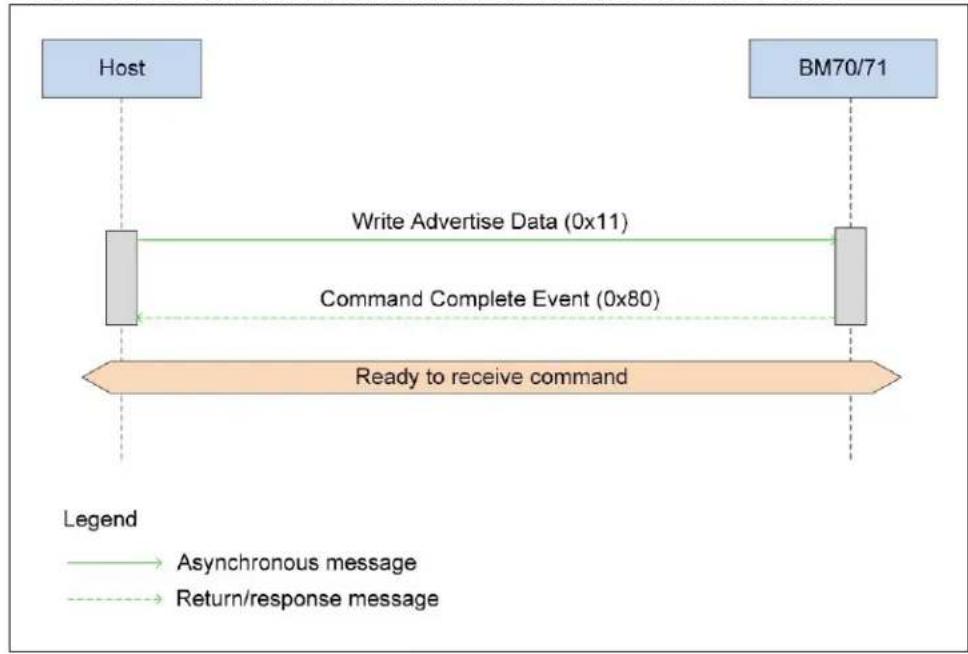
flowchart
graph TD
    A["Host"] -->|Write Advertise Data (0x11)| B["BM70/71"]
    B -->|Command Complete Event (0x80)| A
    A -->|Ready to receive command| B
    style A fill:#e6f3ff,stroke:#333
    style B fill:#e6f3ff,stroke:#333
    linkStyle 0 stroke:#333,stroke-width:2px
    linkStyle 1 stroke:#333,stroke-width:2px
    linkStyle 2 stroke:#333,stroke-width:2px
    linkStyle 3 stroke:#333,stroke-width:2px
    linkStyle 4 stroke:#333,stroke-width:2px
    linkStyle 5 stroke:#333,stroke-width:2px
    linkStyle 6 stroke:#333,stroke-width:2px
    linkStyle 7 stroke:#333,stroke-width:2px
    linkStyle 8 stroke:#333,stroke-width:2px
    linkStyle 9 stroke:#333,stroke-width:2px
    linkStyle 10 stroke:#333,stroke-width:2px
    linkStyle 11 stroke:#333,stroke-width:2px
    linkStyle 12 stroke:#333,stroke-width:2px
    linkStyle 13 stroke:#333,stroke-width:2px
    linkStyle 14 stroke:#333,stroke-width:2px
    linkStyle 15 stroke:#333,stroke-width:2px
    linkStyle 16 stroke:#333,stroke-width:2px
    linkStyle 17 stroke:#333,stroke-width:2px
    linkStyle 18 stroke:#333,stroke-width:2px
    linkStyle 19 stroke:#333,stroke-width:2px
    linkStyle 20 stroke:#333,stroke-width:2px
    linkStyle 21 stroke:#333,stroke-width:2px
    linkStyle 22 stroke:#333,stroke-width:2px
    linkStyle 23 stroke:#333,stroke-width:2px
    linkStyle 24 stroke:#333,stroke-width:2px
    linkStyle 25 stroke:#333,stroke-width:2px
    linkStyle 26 stroke:#333,stroke-width:2px
    linkStyle 27 stroke:#333,stroke-width:2px
    linkStyle 28 stroke:#333,stroke-width:2px
    linkStyle 29 stroke:#333,stroke-width:2px
    linkStyle 30 stroke:#333,stroke-width:2px
    linkStyle 31 stroke:#333,stroke-width:2px
    linkStyle 32 stroke:#333,stroke-width:2px
    linkStyle 33 stroke:#333,stroke-width:2px
    linkStyle 34 stroke:#333,stroke-width:2px
    linkStyle 35 stroke:#333,stroke-width:2px
    linkStyle 36 stroke:#333,stroke-width:2px
    linkStyle 37 stroke:#333,stroke-width:2px
    linkStyle 38 stroke:#333,stroke-width:2px
    linkStyle 39 stroke:#333,stroke-width:2px
    linkStyle 40 stroke:#333,stroke-width:2px
    linkStyle 41 stroke:#333,stroke-width:2px
    linkStyle 42 stroke:#333,stroke-width:2px
    linkStyle 43 stroke:#333,stroke-width:2px
    linkStyle 44 stroke:#333,stroke-width:2px
    linkStyle 45 stroke:#333,stroke-width:2px
    linkStyle 46 stroke:#333,stroke-width:2px
    linkStyle 47 stroke:#333,stroke-width:2px
    linkStyle 48 stroke:#333,stroke-width:2px
    linkStyle 49 stroke:#333,stroke-width:2px
    linkStyle 50 stroke:#333,stroke-width:2px
2.3.3.16.4 Response Format, BM70/71 Module to Host
The BM70/71 module returns the Command Complete Event (0x80) response and does not append the additional data to the event response. For more information on format of response, refer to 2.3.3.51 "Command Complete Event (opcode - 0x80)".
2.3.3.16.5 Applicable Configuration
This command is only available in Manual Operation.
2.3.3.17 WRITE SCAN RESPONSE DATA (OPCODE - 0X12)
This command is used by the host to write data into the available payload of the scan request packet. The data written can be up to 31 bytes in length and there is no limitation to the type of data which can be written. If it requests, the scan request packet is only sent to the remote device.
2.3.3.17.1 Command Format, Host to BM70/71 Module
Table 2-46 provides details of the command format from the host to the BM70/71 module.
TABLE 2-46: COMMAND FORMAT, HOST TO BM70/71 MODULE
| Start Length (H) Length (L) OP Code Parameter | Checksum | |||||
| Byte No | 0 | 1 | 2 | 3 | 4 to n | 5 |
| Value | 0xAA | 0x00 | 0x03 to 0x21 | 0x12 | see Table 2-47 | value |
Table 2-47 provides the parameter values and lengths.
TABLE 2-47: PARAMETER VALUES AND LENGTHS
| Value of Parameter | Parameter Description | Length |
| Value of Parameter (4) | ||
| 0xXX | 0x00 – Reserved for future use | 1 byte |
| Value of Parameter (5 to n) | ||
| 0xXX | Scan response data to be sent | Length = (n - 5)byte(s), 31 bytes(max) |
2.3.3.17.2 Defaults
This does not apply to this command.
2.3.3.17.3 Example
Figure 2-21 illustrates an example of writing scan response data from the host to the BM70/71 module.
FIGURE 2-21: SEQUENCE DIAGRAM OF WRITE SCAN RESPONSE DATA
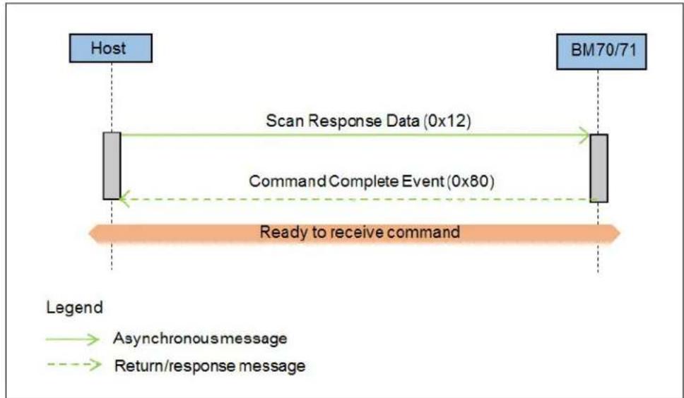
flowchart
graph LR
    A["Host"] -->|Scan Response Data (0x12)| B["BM70/71"]
    B -->|Command Complete Event (0x80)| A
    A -->|Ready to receive command| B
    style A fill:#4CAF50,stroke:#333
    style B fill:#4CAF50,stroke:#333
    linkStyle 0 stroke:#FFA500,stroke-width:2px
    linkStyle 1 stroke:#FFA500,stroke-width:2px
    linkStyle 2 stroke:#FFA500,stroke-width:2px
    linkStyle 3 stroke:#FFA500,stroke-width:2px
    linkStyle 4 stroke:#FFA500,stroke-width:2px
    linkStyle 5 stroke:#FFA500,stroke-width:2px
    linkStyle 6 stroke:#FFA500,stroke-width:2px
    linkStyle 7 stroke:#FFA500,stroke-width:2px
    linkStyle 8 stroke:#FFA500,stroke-width:2px
    linkStyle 9 stroke:#FFA500,stroke-width:2px
    linkStyle 10 stroke:#FFA500,stroke-width:2px
    linkStyle 11 stroke:#FFA500,stroke-width:2px
    linkStyle 12 stroke:#FFA500,stroke-width:2px
    linkStyle 13 stroke:#FFA500,stroke-width:2px
    linkStyle 14 stroke:#FFA500,stroke-width:2px
    linkStyle 15 stroke:#FFA500,stroke-width:2px
    linkStyle 16 stroke:#FFA500,stroke-width:2px
    linkStyle 17 stroke:#FFA500,stroke-width:2px
    linkStyle 18 stroke:#FFA500,stroke-width:2px
    linkStyle 19 stroke:#FFA500,stroke-width:2px
    linkStyle 20 stroke:#FFA500,stroke-width:2px
    linkStyle 21 stroke:#FFA500,stroke-width:2px
    linkStyle 22 stroke:#FFA500,stroke-width:2px
    linkStyle 23 stroke:#FFA500,stroke-width:2px
    linkStyle 24 stroke:#FFA500,stroke-width:2px
    linkStyle 25 stroke:#FFA500,stroke-width:2px
    linkStyle 26 stroke:#FFA500,stroke-width:2px
    linkStyle 27 stroke:#FFA500,stroke-width:2px
    linkStyle 28 stroke:#FFA500,stroke-width:2px
    linkStyle 29 stroke:#FFA500,stroke-width:2px
    linkStyle 30 stroke:#FFA500,stroke-width:2px
    linkStyle 31 stroke:#FFA500,stroke-width:2px
    linkStyle 32 stroke:#FFA500,stroke-width:2px
    linkStyle 33 stroke:#FFA500,stroke-width:2px
    linkStyle 34 stroke:#FFA500,stroke-width:2px
    linkStyle 35 stroke:#FFA500,stroke-width:2px
    linkStyle 36 stroke:#FFA500,stroke-width:2px
    linkStyle 37 stroke:#FFA500,stroke-width:2px
    linkStyle 38 stroke:#FFA500,stroke-width:2px
    linkStyle 39 stroke:#FFA500,stroke-width:2px
    linkStyle 40 stroke:#FFA500,stroke-width:2px
    linkStyle 41 stroke:#FFA500,stroke-width:2px
    linkStyle 42 stroke:#FFA500,stroke-width:2px
    linkStyle 43 stroke:#FFA500,stroke-width:2px
    linkStyle 44 stroke:#FFA500,stroke-width:2px
    linkStyle 45 stroke:#FFA500,stroke-width:2px
    linkStyle 46 stroke:#FFA500,stroke-width:2px
    linkStyle 47 stroke:#FFA500,stroke-width:2px
    linkStyle 48 stroke:#FFA500,stroke-width:2px
    linkStyle 49 stroke:#FFA500,stroke-width:2px
    linkStyle 50 stroke:#FFA500,stroke-width:2px
2.3.3.17.4 Response Format, BM70/71 Module to Host
The BM70/71 module returns the Command Complete Event(0x80) response and does not append the additional data to the event response. For more information on format of the response, refer to 2.3.3.51 "Command Complete Event (opcode - 0x80)".
2.3.3.17.5 Applicable Configuration
This command is only available in Manual Operation.
2.3.3.18 SET ADVERTISING PARAMETERS (OPCODE - 0X13)
This command is used to setup the advertising parameters of the BM70/71 module. This command can only be sent by the host while the BM70/71 module is in "Idle mode" in the Standby state. For directed advertising, the Bluetooth address can be public or random. For random, the BM70/71 module only supports a static random address for directed advertising. The BM70/71 module cannot resolve a "Resolvable private address" as described in the Bluetooth Low Energy specification due to a hardware limitation.
2.3.3.18.1 Command Format, Host to BM70/71 Module
Table 2-48 provides the details of the command format, from the host to the BM70/71 module.
TABLE 2-48: COMMAND FORMAT, HOST TO BM70/71 MODULE
| Start Length (H) Length (L) OP Code Parameter | Checksum | |||||
| Byte No 0 1 2 | 3 | 4 to n | 5 | |||
| Value | 0xAA | 0x00 | 0x0C | 0x13 | see Table 2-49 | value |
Table 2-49 provides the parameter values and lengths.
TABLE 2-49: PARAMETER VALUES AND LENGTHS
| Value of Parameter | Parameter Description | Length |
| Value of Parameter (4 to 5) | ||
| 0xXX | Advertising Interval for undirected advertising.Range - 0x0020 (20 ms) - 4000 (10.24 s)Interval = value * 0.000625Parameter 4 is MSBParameter 5 is LSB | 2 bytes |
| Value of Parameter (6) | ||
| 0x00 | Connectable undirected advertising | 1 byte |
| 0x01 | Connectable directed advertising | |
| 0x02 | Scannable undirected advertising | |
| 0x03 | Non connectable undirected advertising.Setting this value puts the BM70/71 module into broadcast mode | |
| 0x04 | Proprietary beacon setting | |
| Value of Parameter (7) | ||
| 0x00 | Public Device Address | 1 byte |
| 0x01 | Random Device Address | |
| Value of Parameter (8) | ||
| 0xXX XX XX XX XX XX | Device address of the device to be direct these advertising packets to | 6 bytes |
2.3.3.18.2 Default
The default value for the advertising interval is 0x0800 (1.28 seconds), unless set by the host.
2.3.3.18.3 Example
Figure 2-22 illustrates an example of setting the advertising parameters from the host to the BM70/71 module.
FIGURE 2-22: SEQUENCE DIAGRAM OF SET ADVERTISING DATA

flowchart
graph LR
    A["Host"] -->|Set Advertising Data (0x13)| B["BM70/71"]
    B -->|Command Complete Event (0x80)| A
    A -->|Ready to receive command| B
    style A fill:#99ccff,stroke:#333
    style B fill:#99ccff,stroke:#333
    note right of A: Legend: Asynchronous message
    note right of B: Return/response message
2.3.3.18.4 Response Format, BM70/71 Module to Host
The BM70/71 module returns the Command Complete Event (0x80) response and does not append the additional data to the event response. For more information on format of response, refer to 2.3.3.51 "Command Complete Event (opcode - 0x80)".
2.3.3.18.5 Applicable Configuration
This command is only available in Manual Operation.
2.3.3.19 SET SCAN PARAMETERS (OPCODE - 0X15)
This command is used by the host to set up the scan parameters of the BM70/71 module. This command is only valid when the BM70/71 module is in "Idle mode" in the Standby state. To enable scanning, the host uses the Set Scan Enable(0x16) command.
2.3.3.19.1 Command Format, Host to BM70/71 Module
Table 2-50 provides details of the command format from the host to the BM70/71 module.
TABLE 2-50: COMMAND FORMAT, HOST TO BM70/71 MODULE
| Start Length (H) | Length (L) | OP Code | Parameter | Checksum | ||
| Byte No | 0 | 1 | 2 | 3 | 4 to n | 5 |
| Value | 0xAA | 0x00 | 0x06 | 0x15 | see Table 2-51 | value |
Table2-51 provides the parameter values and lengths.
TABLE 2-51: PARAMETER VALUES AND LENGTHS
| Value of Parameter | Parameter Description | Length |
| Value of Parameter (4 to 5) | ||
| 0xXX | This is the scan interval. This represents how often the BM70/71 module will perform the scanRange - 0x0004 (2.5 ms) - 4000 (10.24s)Interval = value * 0.000625Parameter 4 is MSBParameter 5 is LSB | 2 bytes |
| Value of Parameter (5 to 6) | ||
| 0xXX | This is the duration of time; the device will be scanning for, when the scanning interval (scan window) occurs. This value must be less than or equal to the scan interval time period.Range - 0x0004 (2.5 ms) - 4000 (10.24s)Interval = value * 0.000625Parameter 4 is MSBParameter 5 is LSB | 2 bytes |
| Value of Parameter (7) | ||
| 0x00 | Passive scanning. No scan request packets can be sent | 1 byte |
| 0x01 | Active Scanning. Scan Request packets may be sent | |
2.3.3.19.2 Defaults
The default value for the scanning interval is 0x0010 (10 ms), unless set by the host. The default value for the scan window is 0x0010 (10 ms). The default value for the scan type is Passive Scanning(0x01).
2.3.3.19.3 Example
Figure 2-23 illustrates an example of setting scan parameters from the host to the BM70/71 module.
FIGURE 2-23: SEQUENCE DIAGRAM OF SET SCAN PARAMETERS
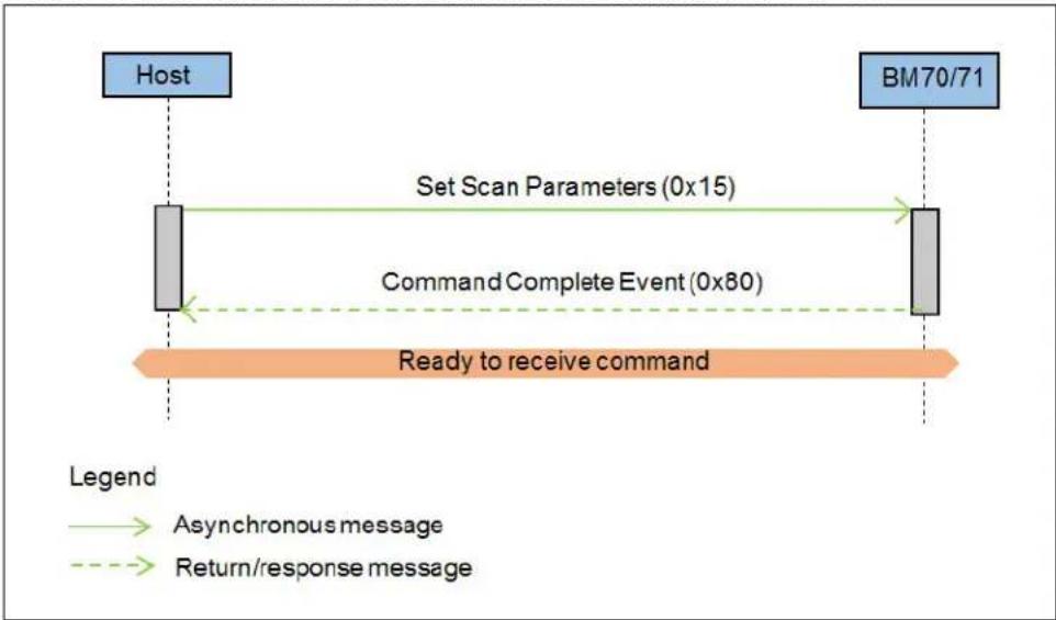
flowchart
graph LR
    A["Host"] --> B["Set Scan Parameters (0x15)"]
    B --> C["Command Complete Event (0x80)"]
    C --> D["Ready to receive command"]
    D --> E["Return/response message"]
    style A fill:#4CAF50,stroke:#333
    style B fill:#4CAF50,stroke:#333
    style C fill:#4CAF50,stroke:#333
    style D fill:#FFA500,stroke:#333
    style E fill:#FFA500,stroke:#333
2.3.3.19.4 Response Format, BM70/71 Module to Host
The BM70/71 module returns the Command Complete Event(0x80) response and does not append the additional data to the event response. For more information on the format of response, refer to 2.3.3.51 "Command Complete Event (opcode - 0x80)".
2.3.3.19.5 Applicable Configuration
This command is only available in Manual Operation.
2.3.3.20 SET SCAN ENABLE (OPCODE - 0X16)
This command is used to enable or disable the scanning process on the BM70/71 module. When performing this, it will cause the BM70/71 module to start or terminate the discovery procedure as defined by the Bluetooth Low Energy specification.
2.3.3.20.1 Command Format, Host to BM70/71 Module
Table 2-52 provides details of the command format from the host to the BM70/71 module.
TABLE 2-52: COMMAND FORMAT, HOST TO BM70/71 MODULE
| Start Length (H) Length (L) OP Code Parameter | Checksum | |||||
| Byte No 0 1 2 | 3 | 4 to n | 5 | |||
| Value | 0xAA | 0x00 | 0x03 | 0x16 | see Table 2-53 | value |
Table 2-53 provides the parameter values and lengths.
TABLE 2-53: PARAMETER VALUES AND LENGTHS
| Value of Parameter | Parameter Description | Length |
| Value of Parameter (4) | ||
| 0x00 | Scanning is disabled | 1 byte |
| 0x01 | Scanning is enabled | |
| Value of Parameter (5) | ||
| 0x00 | Do not filter advertisement packets. Every received advertisement packet will be sent to the host | 1 byte |
| 0x01 | Filtering out duplicate advertisement packets from the same Bluetooth address | |
2.3.3.20.2 Defaults
This does not apply to this command.
2.3.3.20.3 Example
Figure 2-24 illustrates an example of the Set Scan Enable(0x16) command from the host to the BM70/71 module.
FIGURE 2-24: SEQUENCE DIAGRAM OF SET SCAN ENABLE

flowchart
graph LR
    A["Host"] -->|Set Scan Enable (0x16)| B["BM70/71"]
    B -->|Status Report Event (0x81)| A
    A -->|Command Complete Event (0x80)| B
    B -->|Ready to receive command| A
    style A fill:#99ccff,stroke:#333
    style B fill:#99ccff,stroke:#333
2.3.3.20.4 Response Format, BM70/71 Module to Host
The BM70/71 module returns the Command Complete Event (0x80) and the Status Report Event (0x81) response. The BM70/71 module returns the Command Complete Event (0x80) response when it has processed the command from the host. After the Status Report Event (0x81) and Command Complete Event (0x80), the BM70/71 starts sending the results of the advertising scan with the Advertising Report event (0x70). This command does not append additional data to the Command Complete Event (0x80) response. For more information on the format of event responses and possible values, refer to 2.3.3.51 "Command Complete Event (opcode - 0x80)", 2.3.3.52 "Status Report Event (opcode - 0x81)" and 2.3.3.47 "Advertising Report Event (opcode - 0x70)".
2.3.3.20.5 Applicable Configuration
This command is only available in Manual Operation.
2.3.3.21 LE CREATE CONNECTION (OPCODE - 0X17)
This command is used by the host to have the BM70/71 module initiate a connection with a remote device detected during the discovery procedure. For the Bluetooth address parameter in this command, the address of the peer device can be public or random. For random, the BM70/71 module only supports a static random address for creating a connection. The BM70/71 module cannot resolve a "Resolvable private address" as described in the Bluetooth Low Energy specification due to a hardware limitation.
2.3.3.21.1 Command Format, Host to BM70/71 Module
Table 2-54 provides details of the command format from the host to the BM70/71 module.
TABLE 2-54: COMMAND FORMAT, HOST TO BM70/71 MODULE
| Start Length (H) Length (L) OP Code Parameter | Checksum | |||||
| Byte No 0 1 2 | 3 | 4 to n | n+1 | |||
| Value | 0xAA | 0x00 | 0x09 | 0x17 | see Table 2-55 | value |
Table 2-55 provides the parameter values and lengths.
TABLE 2-55: PARAMETER VALUES AND LENGTHS
| Value of Parameter | Parameter Description | Length |
| Value of Parameter (4) | ||
| 0x00 | Reserved, write as 0x00 | 1 byte |
| Value of Parameter (5) | ||
| 0x00 | Public Device Address | 1 byte |
| 0x01 | Random Device Address | |
| Value of Parameter (6 to 11) | ||
| 0xXX XX XX XX XX XX | Public Device Address | 1 byte |
2.3.3.21.2 Default
This does not apply to this command.
2.3.3.21.3 Example
Figure 2-25 illustrates an example of the LE Create Connection (0x17) command from the host to the BM70/71 module.
FIGURE 2-25: SEQUENCE DIAGRAM OF LE CREATE CONNECTION
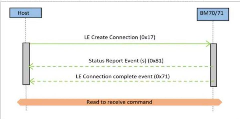
flowchart
graph LR
    A["Host"] -->|LE Create Connection (0x17)| B["BM70/71"]
    B -->|Status Report Event (s) (0x81)| A
    A -->|LE Connection complete event (0x71)| B
    B -->|Read to receive command| A
2.3.3.21.4 Response Format, BM70/71 Module to Host
The BM70/71 module returns an LE Connection Complete Event(0x71) response to the host when a connection with a peer device was attempted. This command indicates if the execution was successful or not. If successful, the parameters associated with the connected peer device are returned as well. For more information about the format of event responses and parameters, refer to 2.3.3.48 "LE Connection Complete Event (opcode - 0x71)".
2.3.3.21.5 Applicable Configuration
This command is only available in Manual Operation.
2.3.3.22 LE CREATE CONNECTION CANCEL (OPCODE - 0X18)
This command is used to cancel the LE Create Connection(0x17) command. This command can only be issued by the host after the LE Create Connection (0x17) command has been issued.
2.3.3.22.1 Command Format, Host to BM70/71 Module
Table 2-56 provides details of the command format from the host to the BM70/71 module.
TABLE 2-56: COMMAND FORMAT, HOST TO BM70/71 MODULE
| Start Length (H) Length (L) OP Code Checksum | |||||
| Byte No | 0 | 1 | 2 | 3 | 5 |
| Value | 0xAA | 0x00 | 0x01 | 0x18 | value |
2.3.3.22.2 Default
This does not apply to this command.
2.3.3.22.3 Example
Figure 2-26 illustrates an example of the LE Cancel Connection (0x18) command from the host to the BM70/71 module.
FIGURE 2-26: SEQUENCE DIAGRAM OF LE CANCEL CONNECTION
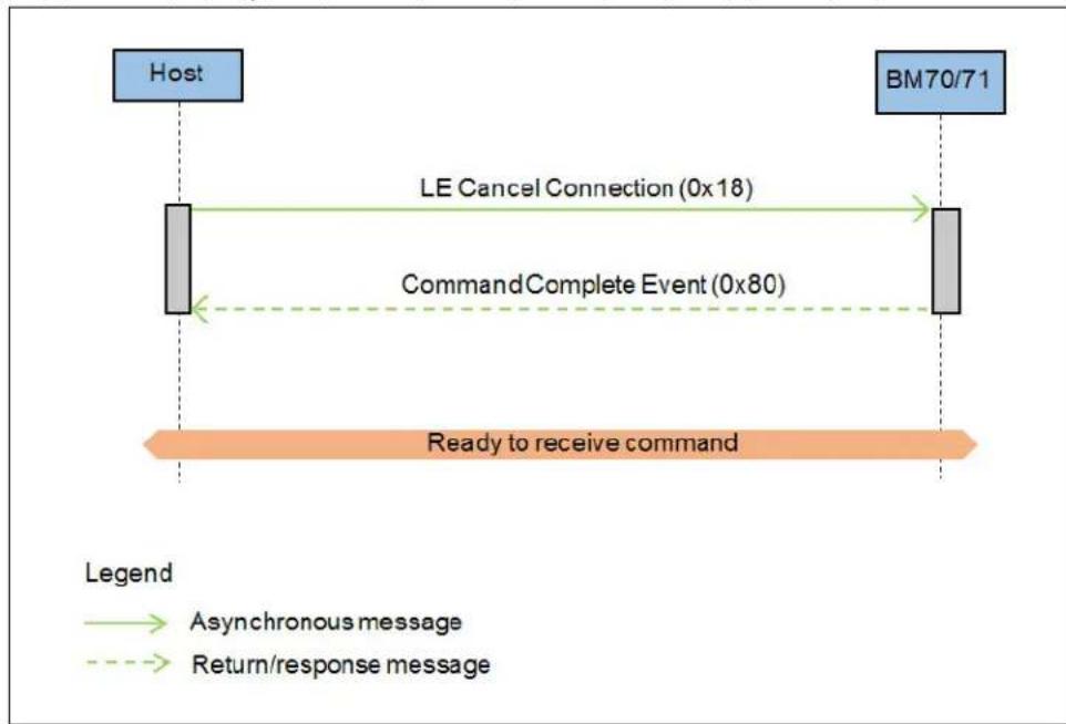
flowchart
graph TD
    A["Host"] -->|LE Cancel Connection (0x18)| B["Command Complete Event (0x80)"]
    B -->|Ready to receive command| C["BM70/71"]
    style A fill:#99ccff,stroke:#333
    style B fill:#99ccff,stroke:#333
    style C fill:#99ccff,stroke:#333
2.3.3.22.4 Response Format, BM70/71 Module to Host
The BM70/71 module returns the Command Complete Event (0x80) response and does not append the additional data to the event response. For more information on the format of the response, refer to 2.3.3.51 "Command Complete Event (opcode - 0x80)".
2.3.3.22.5 Applicable Configuration
This command is only available in Manual Operation.
2.3.3.23 CONNECTION PARAMETER UPDATE REQUEST
(OPCODE - 0X19)
This command is sent by the host to the BM70/71 module to change the connection parameters of the active link. This command is only valid while the Bluetooth link is successfully established between the BM70/71 module and the peer device.
2.3.3.23.1 Command Format, Host to BM70/71 Module
Table 2-57 provides details of the command format from the host to the BM70/71 module.
TABLE 2-57: COMMAND FORMAT, HOST TO BM70/71 MODULE
| Start Length (H) Length (L) OP Code Parameter Checksum | ||||||
| Byte No 0 1 2 | 3 | 4 to 10 | 5 | |||
| Value | 0xAA | 0x00 | 0x08 | 0x19 | see Table 2-58 | value |
Table 2-58 provides the parameter values and lengths.
TABLE 2-58: PARAMETER VALUES AND LENGTHS
| Value of Parameter | Parameter Description | Length |
| Value of Parameter (4) | ||
| 0xXX | Connection Handle | 1 byte |
| Value of Parameter (5 to 6) | ||
| 0xXXXX | Connection Interval is the amount of time between two connection eventsRange - 0x0006 (7.5 ms) - 0x0C80 (4s)Interval = value * 1.25 msParameter 5 is MSBParameter 6 is LSB | 2 bytes |
| Value of Parameter (7 to 8) | ||
| 0xXXXX | Slave Latency is the number of connection events a slave can miss before the connection is considered lostRange: 0x0000 (0 connection events) - 0x01F4 (500 connection events)Parameter 7 is MSBParameter 8 is MSB | 2 bytes |
| Value of Parameter (9 to 10) | ||
| 0xXXXX | Supervision timeout is the maximum amount of time allowed between two packets being received. If this timeout is exceeded and two or more packets have not been received, the connection is considered lost.Range - 0x0006 (7.5 ms) - 0x0C80 (4s)Interval = value * 1.25 msParameter 5 is MSBParameter 6 is LSB | 2 bytes |
2.3.3.23.2 Default
This does not apply to this command.
2.3.3.23.3 Example
Figure 2-27 illustrates an example of the connection parameter update request from the host to the BM70/71 module.
FIGURE 2-27: SEQUENCE DIAGRAM OF CONNECTION PARAMETER UPDATE REQUEST

flowchart
graph TD
    A["Host"] -->|Connection Parameter Update Request (0x19)| B["BM70/71"]
    B -->|Command Complete Event (0x80)| A
    A -->|Connection Parameter Update Event (0x73)| B
    B -->|optional| A
    A -->|Ready to receive command| B
    style A fill:#4CAF50,stroke:#333
    style B fill:#4CAF50,stroke:#333
2.3.3.23.4 Response Format, BM70/71 Module to Host
The BM70/71 module returns the Command Complete Event(0x80) response. If the update was successful, the BM70/71 module will also return the Connection Parameter Update Event(0x73) response. For more information on the format of the response, refer to 2.3.3.50 "Connection Parameter Update Event (opcode - 0x73)" and 2.3.3.51 "Command Complete Event (opcode - 0x80)".
2.3.3.23.5 Applicable Configuration
This command is only available in Manual Operation.
2.3.3.24 DISCONNECT (OPCODE - 0X1B)
This command is used to terminate a connection after the link has been established between the BM70/71 module and a peer device.
2.3.3.24.1 Command Format, Host to BM70/71 Module
Table 2-59 provides details of the command format from the host to the BM70/71 module.
TABLE 2-59: COMMAND FORMAT, HOST TO BM70/71 MODULE
| Start Length (H) | Length (L) | OP Code | Parameter | Checksum | ||
| Byte No | 0 | 1 | 2 | 3 | 4 | 5 |
| Value | 0xAA | 0x00 | 0x01 | 0x1B | 0xXX connection handle | value |
2.3.3.24.2 Default
This does not apply to this command.
2.3.3.24.3 Example
Figure 2-28 illustrates an example of the disconnect event from the host to the BM70/71 module.
FIGURE 2-28: SEQUENCE DIAGRAM OF DISCONNECT EVENT

flowchart
graph TD
    A["Host"] -->|Disconnect (0x1B)| B["BM70/71"]
    B -->|Disconnect Complete Event (0x72)| A
    A -->|Status Report Event (0x81)| B
    B -->|Ready to receive command| A
    style A fill:#99CCFF
    style B fill:#99CCFF
    note right of A: Legend
    linkStyle 0 stroke:#000,stroke-width:2px
    linkStyle 1 stroke:#000,stroke-width:2px
    linkStyle 2 stroke:#000,stroke-width:2px
    linkStyle 3 stroke:#000,stroke-width:2px
    linkStyle 4 stroke:#000,stroke-width:2px
    linkStyle 5 stroke:#000,stroke-width:2px
    linkStyle 6 stroke:#000,stroke-width:2px
    linkStyle 7 stroke:#000,stroke-width:2px
    linkStyle 8 stroke:#000,stroke-width:2px
    linkStyle 9 stroke:#000,stroke-width:2px
    linkStyle 10 stroke:#000,stroke-width:2px
    linkStyle 11 stroke:#000,stroke-width:2px
    linkStyle 12 stroke:#000,stroke-width:2px
    linkStyle 13 stroke:#000,stroke-width:2px
    linkStyle 14 stroke:#000,stroke-width:2px
    linkStyle 15 stroke:#000,stroke-width:2px
    linkStyle 16 stroke:#000,stroke-width:2px
    linkStyle 17 stroke:#000,stroke-width:2px
    linkStyle 18 stroke:#000,stroke-width:2px
    linkStyle 19 stroke:#000,stroke-width:2px
    linkStyle 20 stroke:#000,stroke-width:2px
2.3.3.24.4 Response Format, BM70/71 Module to Host
The BM70/71 module returns the Disconnect Complete(0x72) event and the Status Report Event(0x81) response. The Disconnect Complete(0x72) event response returns when it has processed the command from the host. The BM70/71 module sends the Status Report Event(0x81) when it has finished executing this event. The value returned in the Status Report Event(0x81) message depends on the command processed from the host. For more information on the format of the event responses and possible values, refer to 2.3.3.49 "Disconnect Complete Event (opcode - 0x72)" and 2.3.3.52 "Status Report Event (opcode - 0x81)".
2.3.3.24.5 Applicable Configuration
This command is only available in Manual Operation.
2.3.3.25 SET ADVERTISING ENABLE\_DISABLE (OPCODE - 0X1C)
This command is sent by the host to start or stop the BM70/71 module from sending advertising packets. To enable the BM70/71 module to send advertising packets, the module must be in "Idle mode" of the Standby state. The command Set Advertising Parameter(0x13) will determine the type of advertising packets sent by the BM70/71 module.
2.3.3.25.1 Command Format, Host to BM70/71 Module
Table 2-60 provides details of the command format from the host to the BM70/71 module.
TABLE 2-60: COMMAND FORMAT, HOST TO BM70/71 MODULE
| Start Length (H) Length (L) OP Code Parameter Checksum | ||||||
| Byte No 0 1 2 | 3 | 4 to 10 | 5 | |||
| Value | 0xAA | 0x00 | 0x02 | 0x1C | see Table 2-61 | value |
Table2-61 provides the parameter values and lengths.
TABLE 2-61: PARAMETER VALUES AND LENGTHS
| Value of Parameter (4) | Parameter Description | Length |
| 0x00 | Stop sending advertising packets (BM70/71 module leaves Standby mode, enters Idle mode in the Standby state) | 1 byte |
| 0x01 | Start sending advertising packets (BM70/71 module leaves Idle mode, enters Standby mode in the Standby state) | |
| 0x02 | Start sending advertising packets directed (BM70/71 module leaves Idle mode, enters Standby mode in the Standby state). The BM70/71 module will accept connection requests for a previously paired/bonded device. |
2.3.3.25.2 Default
This does not apply to this command.
2.3.3.25.3 Example
Figure 2-29 and Figure 2-30 illustrate examples of setting advertising packets from the host to the BM70/71 module in Idle mode and Standby mode.
FIGURE 2-29: SEQUENCE DIAGRAM OF SET ADVERTISING PACKETS - IDLE MODE

flowchart
graph TD
    A["Host"] -->|Idle Mode| B["BM70/71"]
    B -->|Command Complete Event (0x80)| A
    A -->|Ready to receive command| B
    B -->|Set Advertising Enable_Disable (0x1C)| A
    A -->|Status Report Event (0x81 – Standby Mode)| B
    B -->|Asynchronous message| A
    B -->|Return/response message| A
FIGURE 2-30: SEQUENCE DIAGRAM OF SET ADVERTISING PACKETS - STANDBY MODE

flowchart
graph TD
    A["Host"] -->|Standby Mode – Sending Advertising Packets| B["BM70/71"]
    B -->|Set Advertising Enable_Disable (0x1C)| A
    A -->|Command Complete Event (0x80)| B
    B -->|Status Report Event (0x81 – Idle Mode)| A
    A -->|Ready to receive command| B
    style A fill:#4A90E2,stroke:#333
    style B fill:#4A90E2,stroke:#333
2.3.3.25.4 Response Format, BM70/71 Module to Host
The BM70/71 module returns the Command Complete Event(0x80) and the Status Report Event(0x81) response. The BM70/71 module returns the Command Complete Event(0x80) response when it has processed the command from the host. The BM70/71 module sends the Status Report Event(0x81) when it has finished executing this event. The value returned in the Status Report Event(0x81) message depends on how the command was processed from the host. This command does not append additional data to the Command Complete Event(0x80) response. For more information on the format of the response, refer to 2.3.3.51 "Command Complete Event (opcode - 0x80)" and 2.3.3.52 "Status Report Event (opcode - 0x81)".
2.3.3.25.5 Applicable Configuration
This command is only available in Manual Operation.
2.3.3.26 READ REMOTE DEVICE NAME (OPCODE - 0X1F)
This command is used to read the remote device name of the peer. This command is only valid while the connection with the peer device is active. A host can use the Read Status Report (0x03) to discover the state of the BM70/71 module to confirm if the connection is active.
2.3.3.26.1 Command Format, Host to BM70/71 Module
Table 2-62 provides details of the command format from the host to the BM70/71 module.
TABLE 2-62: COMMAND FORMAT, HOST TO BM70/71 MODULE
| Start Length (H) Length (L) OP Code Parameter | Checksum | |||||
| Byte No 0 1 | 2 | 3 4 | 5 | |||
| Value | 0xAA | 0x00 | 0x02 | 0x1F | see Table 2-63 | value |
Table 2-63 provides the parameter values and lengths.
TABLE 2-63: PARAMETER VALUES AND LENGTHS
| Value of Parameter (4) | Parameter Description | Length |
| 0xXX | Connection Handle of current connection. This value was returned by the BM70/71 module in an LE Connect Complete Event (0x71) response | 1 byte |
2.3.3.26.2 Default
This does not apply to this command.
2.3.3.26.3 Example
Figure 2-31 illustrates an example of the Read Remote Device Name(0x1F) command from the host to the BM70/71 module.
FIGURE 2-31: SEQUENCE DIAGRAM OF READ REMOTE DEVICE NAME

flowchart
graph TD
    A["Host"] -->|Read Remote Device Name (0x1F)| B["BM70/71"]
    B -->|Command Complete Event (0x80)| A
    A -->|Ready to receive command| B
    style A fill:#99CCFF,stroke:#333
    style B fill:#99CCFF,stroke:#333
2.3.3.26.4 Response Format, BM70/71 Module to Host
The BM70/71 module returns the Command Complete Event(0x80) response and adds the received device name from the peer device in the parameters field. For more information on the base format and values, refer to 2.3.3.51 "Command Complete Event (opcode - 0x80)".
Table 2-64 provides details of the Command Complete Event(0x80) response format from the BM70/71 module to the host.
TABLE 2-64: RESPONSE FORMAT, BM70/71 MODULE TO HOST
| Start Length (H) Length (L) OP Code Parameter Checksum | ||||||
| Byte No 0 1 2 | 3 | 4 to 12 | 5 | |||
| Value | 0xAA | 0x00 | 0x02 to 0xNN | 0x80 | see Table 2-65 | value |
Table 2-65 provides the parameter values and lengths.
TABLE 2-65: PARAMETER VALUES AND LENGTHS
| Value of Parameter (4 to n) | Parameter Description | Length |
| 0x00 | Remote Device Name | 1 byte |
2.3.3.26.5 Applicable Configuration
This command is only available in Manual Operation.
2.3.3.27 GATT CLIENT - DISCOVER ALL PRIMARY SERVICES (OPCODE - 0X30)
This command is used by the host to have the BM70/71 module (client) discover all primary services on a peer device (server).
2.3.3.27.1 Command Format, Host to BM70/71 Module
Table 2-66 provides details of the command format from the host to the BM70/71 module.
TABLE 2-66: COMMAND FORMAT, HOST TO BM70/71 MODULE
| Start Length (H) Length (L) OP Code Parameter | Checksum | |||||
| Byte No 0 1 | 2 | 3 4 | 5 | |||
| Value | 0xAA | 0x00 | 0x02 | 0x30 | see Table 2-67 | value |
Table 2-67 provides the parameter values and lengths.
TABLE 2-67: PARAMETER VALUES AND LENGTHS
| Value of Parameter (4) | Parameter Description | Length |
| 0xXX | Connection Handle of current connection. This value was returned by the BM70/71 module in a LE Connect Complete Event (0x71) response | 1 byte |
2.3.3.27.2 Default
This does not apply to this command.
2.3.3.27.3 Example
Figure 2-32 illustrates an example of the Discover All Primary Services command from the host to the BM70/71 module.
FIGURE 2-32: SEQUENCE DIAGRAM OF GATT CLIENT - DISCOVER ALL PRIMARY SERVICES

flowchart
graph LR
    A["Host"] -->|Discover All Primary Services (0x30)| B["BM70/71"]
    B -->|Command Complete Event (0x80)| A
    A -->|Discover All Primary Services Response (0x90)| B
    B -->|Ready to receive command| A
    style A fill:#4CAF50,stroke:#333
    style B fill:#4CAF50,stroke:#333
    linkStyle 0 stroke:#333,stroke-width:2px
    linkStyle 1 stroke:#333,stroke-width:2px
    linkStyle 2 stroke:#333,stroke-width:2px
    linkStyle 3 stroke:#333,stroke-width:2px
    linkStyle 4 stroke:#333,stroke-width:2px
    linkStyle 5 stroke:#333,stroke-width:2px
    linkStyle 6 stroke:#333,stroke-width:2px
    linkStyle 7 stroke:#333,stroke-width:2px
    linkStyle 8 stroke:#333,stroke-width:2px
    linkStyle 9 stroke:#333,stroke-width:2px
    linkStyle 10 stroke:#333,stroke-width:2px
    linkStyle 11 stroke:#333,stroke-width:2px
    linkStyle 12 stroke:#333,stroke-width:2px
    linkStyle 13 stroke:#333,stroke-width:2px
    linkStyle 14 stroke:#333,stroke-width:2px
    linkStyle 15 stroke:#333,stroke-width:2px
    linkStyle 16 stroke:#333,stroke-width:2px
    linkStyle 17 stroke:#333,stroke-width:2px
    linkStyle 18 stroke:#333,stroke-width:2px
    linkStyle 19 stroke:#333,stroke-width:2px
    linkStyle 20 stroke:#333,stroke-width:2px
    linkStyle 21 stroke:#333,stroke-width:2px
    linkStyle 22 stroke:#333,stroke-width:2px
    linkStyle 23 stroke:#333,stroke-width:2px
    linkStyle 24 stroke:#333,stroke-width:2px
    linkStyle 25 stroke:#333,stroke-width:2px
    linkStyle 26 stroke:#333,stroke-width:2px
    linkStyle 27 stroke:#333,stroke-width:2px
    linkStyle 28 stroke:#333,stroke-width:2px
    linkStyle 29 stroke:#333,stroke-width:2px
    linkStyle 30 stroke:#333,stroke-width:2px
    linkStyle 31 stroke:#333,stroke-width:2px
    linkStyle 32 stroke:#333,stroke-width:2px
    linkStyle 33 stroke:#333,stroke-width:2px
    linkStyle 34 stroke:#333,stroke-width:2px
    linkStyle 35 stroke:#333,stroke-width:2px
    linkStyle 36 stroke:#333,stroke-width:2px
    linkStyle 37 stroke:#333,stroke-width:2px
    linkStyle 38 stroke:#333,stroke-width:2px
    linkStyle 39 stroke:#333,stroke-width:2px
    linkStyle 40 stroke:#333,stroke-width:2px
    linkStyle 41 stroke:#333,stroke-width:2px
    linkStyle 42 stroke:#333,stroke-width:2px
    linkStyle 43 stroke:#333,stroke-width:2px
    linkStyle 44 stroke:#333,stroke-width:2px
    linkStyle 45 stroke:#333,stroke-width:2px
    linkStyle 46 stroke:#333,stroke-width:2px
    linkStyle 47 stroke:#333,stroke-width:2px
    linkStyle 48 stroke:#333,stroke-width:2px
    linkStyle 49 stroke:#333,stroke-width:2px
    linkStyle 50 stroke:#333,stroke-width:2px
2.3.3.27.4 Response Format, BM70/71 Module to Host
The BM70/71 module returns the Command Complete Event(0x80) and the Discover All Primary Services Response Event Response(0x90). The BM70/71 module returns the Command Complete Event(0x80) response when it has processed the command from the host. The BM70/71 module sends the Discover All Primary Services Response Event Response(0x90) when it has received the service list from the peer device. This command does not append additional data to the Command Complete Event(0x80) response. For more information on the format of event responses and possible values, refer to
2.3.3.51 "Command Complete Event (opcode - 0x80)" and 2.3.3.54 "Discover All Primary Services Event (opcode - 0x90)".
2.3.3.27.5 Applicable Configuration
This command is only available in Manual Operation.
2.3.3.28 GATT CLIENT - DISCOVER SPECIFIC PRIMARY
SERVICE CHARACTERISTIC (OPCODE - 0X31)
This command is used to find all characteristic declarations, characteristic descriptor attribute handles, and attribute types within a service definition on a peer device (server) when only the UUID service value is known.
2.3.3.28.1 Command Format, Host to BM70/71 Module
Table 2-68 provides details of the command format from the host to the BM70/71 module.
TABLE 2-68: COMMAND FORMAT, HOST TO BM70/71 MODULE
| Start Length (H) Length (L) OP Code Parameter | Checksum | |||||
| Byte No 0 1 2 | 3 | 4 to n | 5 | |||
| Value | 0xAA | 0x00 | 0x04 to 0x12 | 0x31 | see Table 2-69 | value |
Table 2-69 provides the parameter values and lengths.
TABLE 2-69: PARAMETER VALUES AND LENGTHS
| Value of Parameter | Parameter Description | Length |
| Value of Parameter (4) | ||
| 0xXX | Connection Handle of current connection. This value was returned by the BM70/71 module in an LE Connect Complete Event(0x71) response | 1 byte |
| Value of Parameter (5 - 6) or (5 -22) | ||
| 0xXX | 16-bit Bluetooth UUID or 128-bit UUID | 1 byte |
2.3.3.28.2 Default
This does not apply to this command.
2.3.3.28.3 Example
Figure 2-32 illustrates an example of the discover specific primary service command from the host to BM70/71 module.
FIGURE 2-33: SEQUENCE DIAGRAM OF GATT CLIENT - DISCOVER SPECIFIC PRIMARY SERVICES
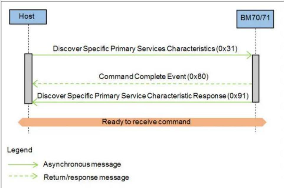
flowchart
graph TD
    A["Host"] --> B["Discover Specific Primary Services Characteristics (0x31)"]
    B --> C["Command Complete Event (0x80)"]
    C --> D["Discover Specific Primary Service Characteristic Response (0x91)"]
    D --> E["Ready to receive command"]
    E --> F["BM70/71"]
    style A fill:#666,stroke:#333
    style B fill:#ccc,stroke:#333
    style C fill:#ccc,stroke:#333
    style D fill:#ccc,stroke:#333
    style E fill:#ccc,stroke:#333
    style F fill:#ccc,stroke:#333
2.3.3.28.4 Response Format, BM70/71 Module to Host
The BM70/71 module returns the Command Complete Event(0x80) and the Discover Specific Primary Services Characteristic Response Event (0x91). The BM70/71 module returns the Command Complete Event(0x80) response when it has processed the command from the host. The BM70/71 module sends the Discover Specific Primary Services Characteristic Response Event(0x91 when it has received the information from the peer device. This command does not append additional data to the Command Complete Event (0x80) response. For more information on the format of event responses and possible values, refer to 2.3.3.51 "Command Complete Event (opcode - 0x80)" and 2.3.3.55 "Discover Specific Primary Service Characteristic Declaration Event (opcode - 0x91)".
2.3.3.28.5 Applicable Configuration
This command is only available in Manual Operation.
2.3.3.29 READ CHARACTERISTIC VALUE (OPCODE - 0X32)
This command is used by the host to have the BM70/71 module read the "Characteristic value" attribute from a peer device (server).
2.3.3.29.1 Command Format, Host to BM70/71 Module
Table 2-70 provides details of the command format from the host to the BM70/71 module.
TABLE 2-70: COMMAND FORMAT, HOST TO BM70/71 MODULE
| Start Length (H) Length (L) OP Code Parameter | Checksum | |||||
| Byte No 0 1 2 | 3 | 4 to 6 | 5 | |||
| Value | 0xAA | 0x00 | 0x05 | 0x32 | see Table 2-71 | value |
Table 2-71 provides the parameter values and lengths.
TABLE 2-71: PARAMETER VALUES AND LENGTHS
| Value of Parameter | Parameter Description | Length |
| Value of Parameter (4) | ||
| 0xXX | Connection Handle of current connection. This value was returned by the BM70/71 module in an LE Connect Complete Event(0x71) response | 1 byte |
| Value of Parameter (5 to 6) | ||
| 0xXXXX | Handle “Characteristic value” attribute | 2 bytes |
2.3.3.29.2 Default
This does not apply to this command.
2.3.3.29.3 Example
Figure 2-34 illustrates an example of the read characteristic value command from the host to the BM70/71 module.
FIGURE 2-34: SEQUENCE DIAGRAM OF READ CHARACTERISTIC VALUE

flowchart
graph TD
    A["Host"] -->|Read Characteristic Value (0x32)| B["BM70/71"]
    B -->|Command Complete Event (0x80)| A
    A -->|Ready to receive command| B
    style A fill:#99ccff,stroke:#333
    style B fill:#99ccff,stroke:#333
2.3.3.29.4 Response Format, BM70/71 Module to Host
The BM70/71 module returns the Command Complete Event (0x80) response and adds the value from the "Characteristic value" attribute in the parameters field. For more information on the base format and values, refer to 2.3.3.51 "Command Complete Event (opcode - 0x80)".
Table 2-72 provides details of the Command Complete Event(0x80) response format from the BM70/71 module to the host.
TABLE 2-72: RESPONSE FORMAT, BM70/71 MODULE TO HOST
| Start Length (H) Length (L) OP Code Parameter Checksum | ||||||
| Byte No | 0 | 1 | 2 | 3 | 4 to 12 | 5 |
| Value | 0xAA | 0x00 | 0x03 to 0x18 | 0x80 | see Table 2-73 | value |
Table 2-73 provides the parameter values and lengths.
TABLE 2-73: PARAMETER VALUES AND LENGTHS
| Value of Parameter | Parameter Description | Length |
| Value of Parameter (4) | ||
| 0xXX | 0x01 - 0xFF, command failure (for table values, refer to Table 2-119) | 1 byte |
| Value of Parameter (5 to 24) | ||
| 0xXX | Value of the “Characteristic value” attribute from the peer device (server), up to 20 bytes max | 1 to 20 bytes |
2.3.3.29.5 Applicable Configuration
This command is only available in Manual Operation.
2.3.3.30 GATT CLIENT - READ USING CHARACTERISTIC UUID (OPCODE - 0X33)
This command is used by the host to have the BM70/71 module (client) read the "Characteristic value" attribute from a peer device (server) when only the characteristic UUID is known.
2.3.3.30.1 Command Format, Host to BM70/71 Module
Table 2-74 provides details of the command format from the host to the BM70/71 module.
TABLE 2-74: COMMAND FORMAT, HOST TO BM70/71 MODULE
| Start Length (H) Length (L) OP Code Parameter | Checksum | |||||
| Byte No 0 1 2 | 3 | 4 to n | 5 | |||
| Value | 0xAA | 0x00 | 0x04 to 0x14 | 0x33 | see Table 2-75 | value |
Table 2-75 provides the parameter values and lengths.
TABLE 2-75: PARAMETER VALUES AND LENGTHS
| Value of Parameter | Parameter Description | Length |
| Value of Parameter (4) | ||
| 0xXX | Connection Handle of current connection. This value was returned by the BM70/71 module in a LE Connect Complete Event(0x71) response | 1 byte |
| Value of Parameter (5 to 6) or (5 to 20) | ||
| 0xXX | Characteristic UUID (16-bit or 128-bit) | 2 or 16 bytes |
2.3.3.30.2 Default
This does not apply to this command.
2.3.3.30.3 Example
Figure 2-35 illustrates an example of the read using characteristic UUID command from the host to BM70/71 module.
FIGURE 2-35: SEQUENCE DIAGRAM OF READ USING CHARACTERISTIC UUID

flowchart
graph TD
    A["Host"] -->|Read Using Characteristic UUID (0x33)| B["BM70/71"]
    B -->|Command Complete Event (0x80)| A
    A -->|Ready to receive command| B
    style A fill:#4CAF50,stroke:#333
    style B fill:#4CAF50,stroke:#333
2.3.3.30.4 Response Format, BM70/71 Module to Host
The BM70/71 module returns the Command Complete Event(0x80) response, and adds the handle and the value from the "Characteristic value" attribute in the parameters field. For more information on the base format and values, refer to
2.3.3.51 "Command Complete Event (opcode - 0x80)".
Table 2-76 provides details of the Command Complete Event(0x80) response format from the BM70/71 module to the host.
TABLE 2-76: RESPONSE FORMAT, BM70/71 MODULE TO HOST
| Start Length (H) | Length (L) | OP Code | Parameter | Checksum | ||
| Byte No | 0 | 1 | 2 | 3 | 4 to 12 | 5 |
| Value | 0xAA | 0x00 | 0x05 to 0x18 | 0x80 | see Table 2-77 | value |
Table 2-77 provides the parameter values and lengths.
TABLE 2-77: PARAMETER VALUES AND LENGTH
| Value of Parameter Parameter Description Length | ||
| Value of Parameter (4) | ||
| 0xXX 0x00 – command successful 1 byte | ||
| Value of Parameter (5 to 6) | ||
| 0xXXXX Value of “Characteristic value” attribute handle | 2 bytes | |
| Value of Parameter (7 to 26) | ||
| 0xXX Value of the “Characteristic value” attribute from the peer device (server), up to 20 bytes max | 1 to 20 bytes | |
2.3.3.30.5 Applicable Configuration
This command is only available in Manual Operation.
2.3.3.31 GATT CLIENT - WRITE CHARACTERISTIC VALUE
(OPCODE - 0X34)
This command is used by a host to have the BM70/71 module (client) write a value to the “Characteristic value” attribute of a peer device (server).
2.3.3.31.1 Command Format, Host to BM70/71 Module
Table 2-78 provides details of the command format from the host to the BM70/71 module.
TABLE 2-78: COMMAND FORMAT, HOST TO BM70/71 MODULE
| Start Length (H) Length (L) OP Code Parameter | Checksum | |||||
| Byte No 0 1 2 | 3 | 4 to n | 5 | |||
| Value | 0xAA | 0x00 | 0x06 to 0x19 | 0x34 | see Table 2-79 | value |
Table 2-79 provides the parameter values and lengths.
TABLE 2-79: PARAMETER VALUES AND LENGTHS
| Value of Parameter | Parameter Description | Length |
| Value of Parameter (4) | ||
| 0xXX | Connection Handle of current connection. This value was returned by the BM70/71 module in a LE Connect Complete Event (0x71) response | 1 byte |
| Value of Parameter (5) | ||
| 0x00 | Write without Response. The client issues a “Write Command” and does need an acknowledgment the write was successful. | 1 byte |
| 0x01 | Write “Characteristic value”. The client issues a “Write request” to the server. The server will respond with a “Write Response” to indicate if the write operation was successful on the “Characteristic value”. | |
| Value of Parameter (6 to 7) | ||
| 0x00 | Handle “Characteristic value” | 2 bytes |
| Value of Parameter (8 to 27) | ||
| 0xXX | “Characteristic value” | 1 to 20 bytes (max) |
2.3.3.31.2 Default
This does not apply to this command.
2.3.3.31.3 Example
Figure 2-36 illustrates an example of the write characteristic value from the host to the BM70/71 module.
FIGURE 2-36: SEQUENCE DIAGRAM OF WRITE CHARACTERISTIC VALUE

flowchart
graph TD
    A["Host"] -->|Write Characteristic Value (0x34)| B["BM70/71"]
    B -->|Command Complete Event (0x80)| A
    A -->|Ready to receive command| B
    style A fill:#99ccff,stroke:#333
    style B fill:#99ccff,stroke:#333
2.3.3.31.4 Response Format, BM70/71 Module to Host
The BM70/71 module returns the Command Complete Event(0x80) response and does not append the additional data to the event response. For more information on the base format and values, refer to 2.3.3.51 "Command Complete Event (opcode - 0x80)".
2.3.3.31.5 Applicable Configuration
This command is only available in Manual Operation.
2.3.3.32 GATT CLIENT - ENABLE TRANSPARENT UART SERVICE (OPCODE - 0X35)
This command is used by a host to have the BM70/71 module (client) write a value to the “Characteristic value” attribute of a peer device (server).
2.3.3.32.1 Command Format, Host to BM70/71 Module
Table 2-80 provides details of the command format from the host to the BM70/71 module.
TABLE 2-80: COMMAND FORMAT, HOST TO BM70/71 MODULE
| Start Length (H) Length (L) OP Code Parameter Checksum | ||||||
| Byte No 0 1 2 | 3 | 4 to 6 | 5 | |||
| Value | 0xAA | 0x00 | 0x04 | 0x35 | see Table 2-81 | value |
Table 2-81 provides the parameter values and lengths.
TABLE 2-81: PARAMETER VALUES AND LENGTHS
| Value of Parameter | Parameter Description | Length |
| Value of Parameter (4) | ||
| 0xXX | Connection Handle of current connection. This value was returned by the BM70/71 module in an LE Connect Complete Event (0x71) response. | 1 byte |
| Value of Parameter (5) | ||
| 0x00 | Disable transparent service on peer device (server) | 1 byte |
| 0x01 | Enable transparent service on peer device (server) | |
| Value of Parameter (6 to 7) | ||
| 0x00 | Client sends transparent data using a “Write Request”. A “Write Response” will be issued by the server to let the client know if the write operation was successful. | 1 byte |
| 0x01 | Client sends the transparent data using a “Write Command”. The client will not get a “Write Response” from the server. | |
2.3.3.32.2 Default
This does not apply to this command.
2.3.3.32.3 Example
Figure 2-37 illustrates an example of the enable "Transparent UART" service command from the host to the BM70/71 module.
FIGURE 2-37: SEQUENCE DIAGRAM OF ENABLE TRANSPARENT UART SERVICE

flowchart
graph TD
    A["Host"] -->|Enable Transparent UART Service (0x35)| B["Command Complete Event (0x80)"]
    B -->|Ready to receive command| C["BM70/71"]
    style A fill:#4CAF50,stroke:#333
    style B fill:#4CAF50,stroke:#333
    style C fill:#4CAF50,stroke:#333
2.3.3.32.4 Response Format, BM70/71 Module to Host
The BM70/71 module returns the Command Complete Event(0x80) response and does not append the additional data to the event response. For more information on the base format and values, refer to 2.3.3.51 "Command Complete Event (opcode - 0x80)".
2.3.3.32.5 Applicable Configuration
This command is only available in Manual Operation.
2.3.3.33 GATT SERVER - SEND CHARACTERISTIC VALUE
(OPCODE - 0X38)
This command is used by the host to have the BM70/71 module (server) send a "Characteristic value" to a peer device (client).
2.3.3.33.1 Command Format, Host to BM70/71 Module
Table 2-82 provides details of the command format from the host to the BM70/71 module.
TABLE 2-82: COMMAND FORMAT, HOST TO BM70/71 MODULE
| Start Length (H) Length (L) OP Code Parameter | Checksum | |||||
| Byte No 0 1 2 | 3 | 4 to 6 | 5 | |||
| Value | 0xAA | 0x00 | 0x05 to 0x18 | 0x38 | see Table 2-83 | value |
Table 2-83 provides the parameter values and lengths.
TABLE 2-83: PARAMETER VALUES AND LENGTHS
| Value of Parameter | Parameter Description | Length |
| Value of Parameter (4) | ||
| 0xXX | Connection Handle of current connection. This value was returned by the BM70/71 module in an LE Connect Complete Event (0x71) response | 1 byte |
| Value of Parameter (5 to 6) | ||
| 0xXXXX | Handle “Characteristic value” attribute | 2 bytes |
| Value of Parameter (7 to 26) | ||
| 0xXX | Value | 1 to 20 bytes (max) |
2.3.3.33.2 Default
This does not apply to this command.
2.3.3.33.3 Example
Figure 2-38 illustrates an example of the send characteristic value command from the host to the BM70/71 module.
FIGURE 2-38: SEQUENCE DIAGRAM OF SEND CHARACTERISTIC VALUE

flowchart
graph TD
    A["Host"] -->|Send Characteristic Value (0x38)| B["BM70/71"]
    B -->|Command Complete Event (0x80)| A
    A -->|Ready to receive command| B
    style A fill:#99ccff,stroke:#333
    style B fill:#99ccff,stroke:#333
2.3.3.33.4 Response Format, BM70/71 Module to Host
The BM70/71 module returns the Command Complete Event(0x80) response and does not append the additional data to the event response. For more information on the base format and values, refer to 2.3.3.51 "Command Complete Event (opcode - 0x80)".
2.3.3.33.5 Applicable Configuration
This command is only available in Manual Operation.
2.3.3.34 GATT SERVER - UPDATE CHARACTERISTIC VALUE (OPCODE - 0X39)
This command is used by the host to update the value of an existing “Characteristic value” attribute in the service table of the BM70/71 module.
2.3.3.34.1 Command Format, Host to BM70/71 Module
Table 2-84 provides details of the command format from the host to the BM70/71 module.
TABLE 2-84: COMMAND FORMAT, HOST TO BM70/71 MODULE
| Start Length (H) Length (L) OP Code Parameter | Checksum | |||||
| Byte No 0 1 2 | 3 | 4 to n | 5 | |||
| Value | 0xAA | 0x00 | 0x03 to 0x16 | 0x39 | see Table 2-85 | value |
Table 2-85 provides the parameter values and lengths.
TABLE 2-85: PARAMETER VALUES AND LENGTHS
| Value of Parameter | Parameter Description | Length |
| Value of Parameter (4) | ||
| 0xXX | Connection Handle of current connection. This value was returned by the BM70/71 module in an LE Connect Complete Event (0x71) response | 1 byte |
| Value of Parameter (5 to 24) | ||
| 0xXX | Value | 1 to 20 bytes (max) |
2.3.3.34.2 Default
This does not apply to this command.
2.3.3.34.3 Example
Figure 2-39 illustrates an example of updating the characteristic value from the host to the BM70/71 module.
FIGURE 2-39: SEQUENCE DIAGRAM OF UPDATE CHARACTERISTIC VALUE

flowchart
graph TD
    A["Host"] -->|Update Characteristic Value (0x39)| B["BM70/71"]
    B -->|Command Complete Event (0x80)| A
    A -->|Ready to receive command| B
    style A fill:#4CAF50,stroke:#333
    style B fill:#4CAF50,stroke:#333
    linkStyle 0 stroke:#FFA500,stroke-width:2px
    linkStyle 1 stroke:#FFA500,stroke-width:2px
    linkStyle 2 stroke:#FFA500,stroke-width:2px
    linkStyle 3 stroke:#FFA500,stroke-width:2px
    linkStyle 4 stroke:#FFA500,stroke-width:2px
    linkStyle 5 stroke:#FFA500,stroke-width:2px
    linkStyle 6 stroke:#FFA500,stroke-width:2px
    linkStyle 7 stroke:#FFA500,stroke-width:2px
    linkStyle 8 stroke:#FFA500,stroke-width:2px
    linkStyle 9 stroke:#FFA500,stroke-width:2px
    linkStyle 10 stroke:#FFA500,stroke-width:2px
    linkStyle 11 stroke:#FFA500,stroke-width:2px
    linkStyle 12 stroke:#FFA500,stroke-width:2px
    linkStyle 13 stroke:#FFA500,stroke-width:2px
    linkStyle 14 stroke:#FFA500,stroke-width:2px
    linkStyle 15 stroke:#FFA500,stroke-width:2px
    linkStyle 16 stroke:#FFA500,stroke-width:2px
    linkStyle 17 stroke:#FFA500,stroke-width:2px
    linkStyle 18 stroke:#FFA500,stroke-width:2px
    linkStyle 19 stroke:#FFA500,stroke-width:2px
    linkStyle 20 stroke:#FFA500,stroke-width:2px
    linkStyle 21 stroke:#FFA500,stroke-width:2px
    linkStyle 22 stroke:#FFA500,stroke-width:2px
    linkStyle 23 stroke:#FFA500,stroke-width:2px
    linkStyle 24 stroke:#FFA500,stroke-width:2px
    linkStyle 25 stroke:#FFA500,stroke-width:2px
    linkStyle 26 stroke:#FFA500,stroke-width:2px
    linkStyle 27 stroke:#FFA500,stroke-width:2px
    linkStyle 28 stroke:#FFA500,stroke-width:2px
    linkStyle 29 stroke:#FFA500,stroke-width:2px
    linkStyle 30 stroke:#FFA500,stroke-width:2px
    linkStyle 31 stroke:#FFA500,stroke-width:2px
    linkStyle 32 stroke:#FFA500,stroke-width:2px
    linkStyle 33 stroke:#FFA500,stroke-width:2px
    linkStyle 34 stroke:#FFA500,stroke-width:2px
    linkStyle 35 stroke:#FFA500,stroke-width:2px
    linkStyle 36 stroke:#FFA500,stroke-width:2px
    linkStyle 37 stroke:#FFA500,stroke-width:2px
    linkStyle 38 stroke:#FFA500,stroke-width:2px
    linkStyle 39 stroke:#FFA500,stroke-width:2px
    linkStyle 40 stroke:#FFA500,stroke-width:2px
    linkStyle 41 stroke:#FFA500,stroke-width:2px
    linkStyle 42 stroke:#FFA500,stroke-width:2px
    linkStyle 43 stroke:#FFA500,stroke-width:2px
    linkStyle 44 stroke:#FFA500,stroke-width:2px
    linkStyle 45 stroke:#FFA500,stroke-width:2px
    linkStyle 46 stroke:#FFA500,stroke-width:2px
    linkStyle 47 stroke:#FFA500,stroke-width:2px
    linkStyle 48 stroke:#FFA500,stroke-width:2px
    linkStyle 49 stroke:#FFA500,stroke-width:2px
    linkStyle 50 stroke:#FFA500,stroke-width:2px
2.3.3.34.4 Response Format, BM70/71 Module to Host
The BM70/71 module returns the Command Complete Event(0x80) response and does not append the additional data to the event response. For more information on the base format and values, refer to 2.3.3.51 "Command Complete Event (opcode - 0x80)".
2.3.3.34.5 Applicable Configuration
This command is only available in Manual Operation.
2.3.3.35 GATT SERVER - READ LOCAL CHARACTERISTIC VALUE (OPCODE - 0X3A)
This command is used by the host to have the BM70/71 module read and return the value from the "Characteristic value" attribute.
2.3.3.35.1 Command Format, Host to BM70/71 Module
Table 2-86 provides details of the command format from the host to the BM70/71 module.
TABLE 2-86: COMMAND FORMAT, HOST TO BM70/71 MODULE
| Start Length (H) | Length (L) | OP Code | Parameter | Checksum | ||
| Byte No | 0 | 1 | 2 | 3 | 4 to 5 | 5 |
| Value | 0xAA | 0x00 | 0x03 | 0x3A | see Table 2-87 | value |
Table 2-87 provides the parameter values and lengths.
TABLE 2-87: PARAMETER VALUES AND LENGTHS
| Value of Parameter (4 to 5) | Parameter Description | Length |
| 0xXXXX | Handle “Characteristic value” attribute (Formatted as big endian) | 2 bytes |
2.3.3.35.2 Default
This does not apply to this command.
2.3.3.35.3 Example
Figure 2-40 illustrates an example of the read local characteristic command from the host to the BM70/71 module.
flowchart
graph TD
    A["Host"] -->|Read Local Characteristic Value (0x3A)| B["BM70/71"]
    B -->|Command Complete Event (0x80)| A
    A -->|Ready to receive command| B
    style A fill:#99CCFF
    style B fill:#99CCFF
    note right of A: Legend
    linkStyle 0 stroke:#000,stroke-width:2px
    linkStyle 1 stroke:#000,stroke-width:2px
    linkStyle 2 stroke:#000,stroke-width:2px
    linkStyle 3 stroke:#000,stroke-width:2px
    linkStyle 4 stroke:#000,stroke-width:2px
    linkStyle 5 stroke:#000,stroke-width:2px
    linkStyle 6 stroke:#000,stroke-width:2px
    linkStyle 7 stroke:#000,stroke-width:2px
    linkStyle 8 stroke:#000,stroke-width:2px
    linkStyle 9 stroke:#000,stroke-width:2px
    linkStyle 10 stroke:#000,stroke-width:2px
    linkStyle 11 stroke:#000,stroke-width:2px
    linkStyle 12 stroke:#000,stroke-width:2px
    linkStyle 13 stroke:#000,stroke-width:2px
    linkStyle 14 stroke:#000,stroke-width:2px
    linkStyle 15 stroke:#000,stroke-width:2px
    linkStyle 16 stroke:#000,stroke-width:2px
    linkStyle 17 stroke:#000,stroke-width:2px
    linkStyle 18 stroke:#000,stroke-width:2px
    linkStyle 19 stroke:#000,stroke-width:2px
    linkStyle 20 stroke:#000,stroke-width:2px
2.3.3.35.4 Response Format, BM70/71 Module to Host
The BM70/71 module returns the Command Complete Event(0x80) response and adds the value from the requested "Characteristic value" attribute in the parameters field. For more information on the base format and values, refer to
2.3.3.51 "Command Complete Event (opcode - 0x80)".
Table 2-88 provides details of the Command Complete Event(0x80) response format from the BM70/71 module to the host.
TABLE 2-88: RESPONSE FORMAT, BM70/71 MODULE TO HOST
| Start Length (H) Length (L) OP Code Parameter Checksum | ||||||
| Byte No 0 1 2 | 3 | 4 to 12 | 5 | |||
| Value | 0xAA | 0x00 | 0x03 to 0xNN | 0x80 | see Table 2-89 | value |
Table 2-89 provides the parameter values and lengths.
TABLE 2-89: PARAMETER VALUES AND LENGTHS
| Value of Parameter | Parameter Description | Length |
| Value of Parameter (4) | ||
| 0x01 - 0xFF | Command failure (for table values, refer to Table 2-119) | 1 byte |
| Value of Parameter (5 to n) | ||
| 0xXX | Value of “Characteristic value” attribute handle (formatted as big endian) | Length = (n - 5) bytes |
2.3.3.35.5 Applicable Configuration
This command is only available in Manual Operation.
2.3.3.36 GATT SERVER - READ ALL LOCAL PRIMARY SERVICES (OPCODE - 0X3B)
This command is used by the host to read all primary services from the service table of the BM70/71 module.
2.3.3.36.1 Command Format, Host to BM70/71 Module
Table 2-90 provides details of the command format from the host to the BM70/71 module.
TABLE 2-90: COMMAND FORMAT, HOST TO BM70/71 MODULE
| Start Length (H) Length (L) OP Code Checksum | |||||
| Byte No | 0 | 1 | 2 | 3 | 4 |
| Value | 0xAA | 0x00 | 0x01 | 0x3B | value |
2.3.3.36.2 Default
This does not apply to this command.
2.3.3.36.3 Example
Figure 2-41 illustrates an example of the read all local primary services command from the host to the BM70/71 module.
FIGURE 2-41: SEQUENCE DIAGRAM OF READ ALL LOCAL PRIMARY SERVICES
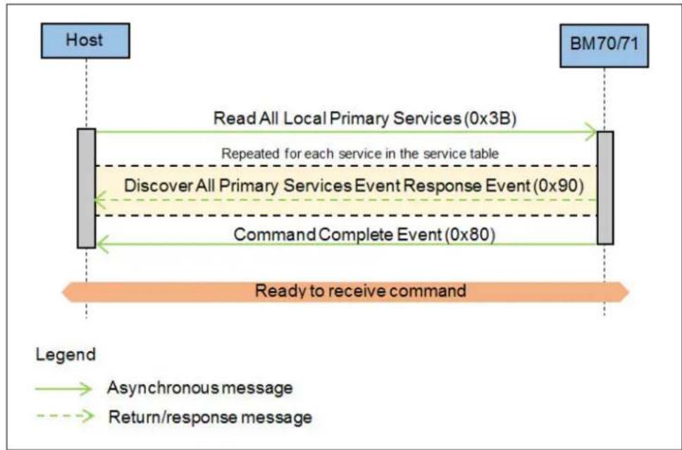
flowchart
graph TD
    A["Host"] -->|Read All Local Primary Services (0x3B)| B["BM70/71"]
    B -->|Repeated for each service in the service table| A
    A -->|Discover All Primary Services Event Response Event (0x90)| B
    B -->|Command Complete Event (0x80)| A
    A -->|Ready to receive command| B
    style A fill:#4A90E2,stroke:#333
    style B fill:#4A90E2,stroke:#333
2.3.3.36.4 Response Format, BM70/71 Module to Host
The BM70/71 module sends the information of the primary services from the service table to the host through a Discover All Primary Services Event Response (0x90). This event response can be repeated several times by the BM70/71 module, based on the number of services in the service table. The host must be capable of handling all Discover All Primary Services Event Response (0x90) sent by the BM70/71 module. When the BM70/71 module has finished sending the primary service list, a Command Complete Event (0x80) response will be sent to the host. For more information on the format of the event responses, refer to
2.3.3.51 "Command Complete Event (opcode - 0x80)" and 2.3.3.54 "Discover All Primary Services Event (opcode - 0x90)".
2.3.3.36.5 Applicable Configuration
This command is only available in Manual Operation.
2.3.3.37 GATT SERVER - READ SPECIFIC LOCAL PRIMARY SERVICE (OPCODE - 0X3C)
This command is used by the host to read the attributes of a specific primary service from the service table of the BM70/71 module.
2.3.3.37.1 Command Format, Host to BM70/71 Module
Table 2-91 provides details of the command format from the host to the BM70/71 module.
TABLE 2-91: COMMAND FORMAT, HOST TO BM70/71 MODULE
| Start Length (H) Length (L) OP Code Parameter | Checksum | |||||
| Byte No | 0 | 1 | 2 | 3 | 4 to n | 5 |
| Value | 0xAA | 0x00 | 0x02 to 0x11 | 0x3C | see Table2-92 | value |
Table 2-92 provides the parameter values and lengths.
TABLE 2-92: PARAMETER VALUES AND LENGTHS
| Value of Parameter (4) or (4 to 19) | Parameter Description | Length |
| 0xXX | 16-bit UUID or 128-bit UUID (Formatted as big endian) | 2 or 16 bytes |
2.3.3.37.2 Default
This does not apply to this command.
2.3.3.37.3 Example
Figure 2-40 illustrates an example of the read specific local primary service command from the host to the BM70/71 module.
FIGURE 2-42: SEQUENCE DIAGRAM OF READ SPECIFIC LOCAL PRIMARY SERVICE

flowchart
graph TD
    A["Host"] -->|Read Specific Local Primary Services (0x3C)| B["BM70/71"]
    B -->|Discover Specific Primary Services Characteristic Declaration Event (0x91)| A
    A -->|Discover All Characteristic Descriptor Response (0x92)| B
    B -->|Command Complete Event (0x80)| A
    A -->|Ready to receive command| B
    style A fill:#4A90E2,stroke:#333
    style B fill:#4A90E2,stroke:#333
2.3.3.37.4 Response Format, BM70/71 Module to Host
The BM70/71 module sends the host the characteristic definition(s) which make the specified primary service through the Discover Specific Primary Service Characteristic Declaration Event(0x91) and Discover All Characteristic Descriptors Event Response(0x92). This information is returned in the event response(s), and the event response(s) which are sent are based upon the attribute types within the characteristic definition(s) of a given service. For example, a characteristic definition is not required to include a "Characteristic descriptor declaration" attribute type. Therefore, the BM70/71 module will return only the Discover Specific Primary Service Characteristic Declaration Event(0x91) to the host.
The host must be capable of handling the various event responses sent by the BM70/71 module. When the BM70/71 module has finished sending the characteristic definition(s) of a specific primary service, a Command Complete Event(0x80) response will be sent to the host. For more information on the format of event responses, refer to 2.3.3.51 "Command Complete Event (opcode - 0x80)", 2.3.3.55 "Discover Specific Primary Service Characteristic Declaration Event (opcode - 0x91)" and 2.3.3.56 "Discover All Characteristic Descriptors Event (opcode - 0x92)".
2.3.3.37.5 Applicable Configuration
This command is only available in Manual Operation.
2.3.3.38 GATT SERVER - SEND WRITE RESPONSE (OPCODE - 0X3D)
The host is informed by the BM70/71 module when a client issues a write request to the value of a specific “Characteristic value” attribute. This command allows the host to reply with a write response and accept or reject the write request. This command is used by the host for the BM70/71 module to inform the peer device (client) whether the write request was successful or not.
2.3.3.38.1 Command Format, Host to BM70/71 Module
Table 2-93 provides details of the command format from the host to the BM70/71 module.
TABLE 2-93: COMMAND FORMAT, HOST TO BM70/71 MODULE
| Start Length (H) Length (L) OP Code Parameter Checksum | ||||||
| Byte No 0 1 2 | 3 | 4 to 8 | 5 | |||
| Value | 0xAA | 0x00 | 0x06 | 0x3D | see Table 2-94 | value |
Table 2-94 provides the parameter values and lengths.
TABLE 2-94: PARAMETER VALUES AND LENGTHS
| Value of Parameter | Parameter Description | Length |
| Value of Parameter (4) | ||
| 0xXX | Connection Handle of current connection. This value was returned by the BM70/71 module in an LE Connect Complete Event (0x71) response. | 1 byte |
| Value of Parameter (5) | ||
| 0x12 | Write request opcode. This is a fixed value and must be set to 0x12 for this command to succeed. | 1 byte |
| Value of Parameter (6 to 7) | ||
| 0xXXXX | Handle the “Characteristic value” attribute which was requested to write | 2 bytes |
| Value of Parameter (8) | ||
| 0x00 | No error. BM70/71 module will send the write response to peer device (client). | 1 byte |
| 0x01 | Invalid Handle | |
| 0x02 | Read not permitted | |
| 0x03 | Write not permitted | |
| 0x04 | Invalid PDU | |
| 0x05 | Insufficient Authentication | |
| 0x06 | Request not supported | |
| 0x07 | Invalid Offset | |
| 0x08 | Insufficient Authorization | |
| 0x09 | Prepare queue full | |
| 0x0A | Attribute not found | |
| 0x0B | Attribute not long | |
| 0x0C | Insufficient encryption Key size | |
| 0x0D | Invalid Attribute value length | |
| 0x0E | Unlikely error | |
TABLE 2-94: PARAMETER VALUES AND LENGTHS
| Value of Parameter Parameter Description Length | |
| 0x0F Insufficient encryption 1 byte | |
| 0x10 Unsupported Group type | |
| 0x11 Insufficient Resources | |
| 0x12 to 0x7F Reserved | |
| 0x80 to 0x9F Application defined errors | |
| 0xA0 to 0xDF Reserved | |
| 0xE0 to 0xFF Common profile and Service error codes | |
2.3.3.38.2 Default
This does not apply to this command.
2.3.3.38.3 Example
Figure 2-43 illustrates an example of the send write response command from the host to the BM70/71 module.
FIGURE 2-43: SEQUENCE DIAGRAM OF SEND WRITE RESPONSE

flowchart
graph TD
    A["Host"] -->|Send Write Response (0x3D)| B["BM70/71"]
    B -->|Command Complete Event (0x80)| A
    A -->|Ready to receive command| B
    style A fill:#99ccff,stroke:#333
    style B fill:#99ccff,stroke:#333
2.3.3.38.4 Response Format, BM70/71 Module to Host
The BM70/71 module returns the Command Complete Event(0x80) response and does not append the additional data to the event response. For more information on the base format and values, refer to 2.3.3.51 "Command Complete Event (opcode - 0x80)".
2.3.3.38.5 Applicable Configuration
This command is only available in Manual Operation.
2.3.3.39 TRANSPARENT UART SERVICE - SEND DATA (OPCODE - 0X3F)
This command is used by the host to have the BM70/71 module send data to the peer device using the proprietary “Transparent UART” service.
2.3.3.39.1 Command Format, Host to BM70/71 Module
Table 2-95 provides details of the command format from the host to the BM70/71 module.
TABLE 2-95: COMMAND FORMAT, HOST TO BM70/71 MODULE
| Start Length (H) Length (L) OP Code Parameter Checksum | ||||||
| Byte No 0 1 2 | 3 | 4 to n | 5 | |||
| Value | 0xAA | 0x00 | 0x03 to 0xNN | 0x3F | see Table 2-96 | value |
Table 2-96 provides the parameter values and lengths.
TABLE 2-96: PARAMETER VALUES AND LENGTHS
| Value of Parameter | Parameter Description | Length |
| Value of Parameter (4) | ||
| 0xXX | Connection Handle of current connection. This value was returned by the BM70/71 module in an LE Connect Complete (0x71) event response | 1 byte |
| Value of Parameter (5 to n) | ||
| 0xXX | Data to transmit | 1 to 640 bytes (max) |
2.3.3.39.2 Default
This does not apply to this command.
2.3.3.39.3 Example
Figure 2-44 illustrates an example of the "Transparent UART" service command from the host to the BM70/71 module.
FIGURE 2-44: SEQUENCE DIAGRAM OF SEND WRITE RESPONSE

flowchart
graph TD
    A["Host"] -->|Send Write Response (0x3D)| B["BM70/71"]
    B -->|Command Complete Event (0x80)| A
    A -->|Ready to receive command| B
    style A fill:#99ccff,stroke:#333
    style B fill:#99ccff,stroke:#333
2.3.3.39.4 Response Format, BM70/71 Module to Host
The BM70/71 module returns the Command Complete Event(0x80) response and does not append the additional data to the event response. For more information on the format of the response, refer to 2.3.3.51 "Command Complete Event (opcode - 0x80)".
2.3.3.39.5 Applicable Configuration
This command is only available in Manual Operation.
2.3.3.40 PAIRING - PASSKEY ENTRY RESPONSE (OPCODE - 0X40)
This command is used by the host to inform the BM70/71 module of the Passkey values being entered. For more information on the overview of Security and the Passkey method, refer to 1.1.2.3.6 “General Operation - Security”.
2.3.3.40.1 Command Format, Host to BM70/71 Module
Table 2-97 provides details of the command format from the host to the BM70/71 module.
TABLE 2-97: COMMAND FORMAT, HOST TO BM70/71 MODULE
| Start Length (H) | Length (L) | OP Code | Parameter | Checksum | ||
| Byte No | 0 | 1 | 2 | 3 | 4 to 6 | 5 |
| Value | 0xAA | 0x00 | 0x03 | 0x40 | see Table 2-98 | value |
Table 2-98 provides the parameter values and lengths.
TABLE 2-98: PARAMETER VALUES AND LENGTHS
| Value of Parameter | Parameter Description | Length |
| Value of Parameter (4) | ||
| 0xXX | Connection handle of current connection. This value was returned by the BM70/71 module in an LE Connect Complete Event(0x71) response. | 1 byte |
| Value of Parameter (5) | ||
| 0x01 | Passkey digit entered | 1 byte |
| 0x02 | Passkey digit erased | |
| 0x03 | Passkey cleared | |
| 0x04 | Passkey entry completed | |
| Value of Parameter (6) | ||
| 0x01 | Digit value represented in ASCII. Ignored if parameter (5) is not set to 0x01. | 1 byte |
2.3.3.40.2 Default
This does not apply to this command.
2.3.3.40.3 Example
Figure 2-45 illustrates an example of the passkey entry response from the host to the BM70/71 module.
FIGURE 2-45: SEQUENCE DIAGRAM OF PAIRING - PASSKEY ENTRY RESPONSE

flowchart
graph TD
    A["Host"] --> B["Passkey Key Entry Response"]
    B --> C["Command Complete Event"]
    C --> D["Passkey Key Entry Response (0x40) - Complete"]
    D --> E["Ready to receive command"]
    E --> F["BM70/71"]
    F --> G["Repeated 6 times"]
    style A fill:#99CCFF
    style F fill:#99CCFF
    style G fill:#FFFF99
    style_H["Legend"] --> I["Asynchronous message"]
    H --> J["Return/response message"]
2.3.3.40.4 Response Format, BM70/71 Module to Host
The BM70/71 module returns the Command Complete Event(0x80) response and does not append additional data to the event response. For more information on the format of the response, refer to 2.3.3.51 "Command Complete Event (opcode - 0x80)".
2.3.3.40.5 Applicable Configuration
This command is only available in Manual Operation.
2.3.3.41 PAIRING - USER CONFIRM PASSKEY RESPONSE
(OPCODE - 0X41)
This command is used by the host to confirm the received Passkey value is correct or not. The host receives the Passkey from the BM70/71 module through the Pairing - Passkey Confirm Request Event(0x62). The host then uses this command to accept or reject the received Passkey.
2.3.3.41.1 Command Format, Host to BM70/71 Module
Table 2-99 provides details of the command format from the host to the BM70/71 module.
TABLE 2-99: COMMAND FORMAT, HOST TO BM70/71 MODULE
| Start Length (H) | Length (L) | OP Code | Parameter | Checksum | ||
| Byte No | 0 | 1 | 2 | 3 | 4 to 6 | 5 |
| Value | 0xAA | 0x00 | 0x03 | 0x41 | see Table 2-100 | value |
Table 2-100 provides the parameter values and lengths.
TABLE 2-100: PARAMETER VALUES AND LENGTHS
| Value of Parameter | Parameter Description | Length |
| Value of Parameter (4) | ||
| 0xXX | Connection Handle of current connection. This value was returned by the BM70/71 module in an LE Connect Complete Event (0x71) response. | 1 byte |
| Value of Parameter (5) | ||
| 0x00 | Passkey accepted (YES) | 1 byte |
| 0x01 | Passkey rejected (NO) | |
2.3.3.41.2 Default
This does not apply to this command.
2.3.3.41.3 Example
Figure 2-46 illustrates an example of the user confirm passkey response from the host to the BM70/71 module.
FIGURE 2-46: SEQUENCE DIAGRAM OF PAIRING - PASSKEY RESPONSE

flowchart
sequenceDiagram
    A["Host"] --> B["Passkey Confirm Request Event (0x62)"]
    B --> C["Passkey Confirm Response (0x41)"]
    C --> D["Pairing Complete Event (0x61)"]
    D --> E["Status Report Event (0x81)"]
    E --> F["Ready to receive command"]
    F --> G["BM70/71"]
    style A fill:#99ccff,stroke:#333
    style G fill:#99ccff,stroke:#333
2.3.3.41.4 Response Format, BM70/71 Module to Host
The BM70/71 module returns the Pairing Complete Event (0x61) and the Status Report Event (0x81) response. The BM70/71 module returns the Pairing Complete Event (0x61) response when it has finished the pairing/bonding procedure with the peer device. The BM70/71 module sends the Status Report Event (0x81) when the pairing procedure result has caused an internal status change. The value returned in the Status Report Event (0x81) message depends on how the command from the pairing/bonding procedure was processed. For more information about the format of event responses and possible values, refer to 2.3.3.45 "Pairing - Pair Complete Event (opcode - 0x61)" and 2.3.3.52 "Status Report Event (opcode - 0x81)".
2.3.3.41.5 Applicable Configuration
This command is only available in Manual Operation.
2.3.3.42 PAIRING - PAIR REQUEST (OPCODE - 0X42)
This command is used to initiate the pairing/bonding procedure. This command can only be sent after an active connection has been established with a peer device. This command can be issued by the host at anytime when a higher level of security is needed for an active connection.
2.3.3.42.1 Command Format, Host to BM70/71 Module
Table 2-101 provides details of the command format from the host to the BM70/71 module.
TABLE 2-101: COMMAND FORMAT, HOST TO BM70/71 MODULE
| Start Length (H) Length (L) OP Code Parameter Checksum | ||||||
| Byte No 0 1 2 | 3 | 4 | 5 | |||
| Value | 0xAA | 0x00 | 0x02 | 0x42 | see Table 2-102 | value |
Table 2-102 provides the parameter values and lengths.
TABLE 2-102: PARAMETER VALUES AND LENGTHS
| Value of Parameter (4) | Parameter Description | Length |
| 0xXX | Connection Handle of current connection. This value was returned by the BM70/71 module in an LE Connect Complete Event (0x71) response | 1 byte |
2.3.3.42.2 Default
This does not apply to this command.
2.3.3.42.3 Example
Figure 2-47 illustrates an example of the pairing request from the host to the BM70/71 module.
FIGURE 2-47: SEQUENCE DIAGRAM OF PAIRING REQUEST

flowchart
graph TD
    A["Host"] -->|Pairing Request (0x42)| B["BM70/71"]
    B -->|Command Complete Event (0x80)| A
    A -->|Pairing Complete Event (0x61) (complete, fail, or timeout)| B
    B -->|Ready to receive command| A
    style A fill:#99ccff,stroke:#333
    style B fill:#99ccff,stroke:#333
    note right of A: Legend
    note left of B: Asynchronous message
2.3.3.42.4 Response format, BM70/71 Module to Host
The BM70/71 module returns the Command Complete Event(0x80) response and the Pairing Complete Event(0x61) response. The BM70/71 module returns the Pairing Complete Event(0x61) response when it has finished the pairing/bonding procedure with the peer device. The BM70/71 module sends the Command Complete Event(0x80) response when the BM70/71 module has processed the Pairing Request(0x42) command. For more information about the format of the event responses and possible values, refer to 2.3.3.45 "Pairing - Pair Complete Event (opcode - 0x61)" and 2.3.3.51 "Command Complete Event (opcode - 0x80)".
2.3.3.42.5 Applicable Configuration
This command is only available in Manual Operation.
2.3.3.43 LEAVE CONFIGURE MODE (OPCODE - 0X52)
This command is used by the host to command the BM70/71 module to exit from the "Configuration Window" and start Auto Operation. For information on the description of the "Configuration Window", refer to 1.1.2.1.3 "Auto Operation – Configuration Timeout".
2.3.3.43.1 Command Format, Host to BM70/71 Module
Table 2-103 provides details of the command format from the host to the BM70/71 module.
TABLE 2-103: COMMAND FORMAT, HOST TO BM70/71 MODULE
| Start Length (H) | Length (L) | OP Code | Parameter | Checksum | ||
| Byte No | 0 | 1 | 2 | 3 | 4 | 5 |
| Value | 0xAA | 0x00 | 0x02 | 0x52 | see Table 2-104 | value |
Table 2-104 provides the parameter values and lengths.
TABLE 2-104: PARAMETER VALUES AND LENGTHS
| Value of Parameter (4) | Parameter Description | Length |
| 0x00 | Leave Configure Mode | 1 byte |
| 0x01 | Leave Configure Mode and disable mode forever |
2.3.3.43.2 Default
This does not apply to this command.
2.3.3.43.3 Example
Figure 2-48 illustrates an example of the leave configure mode command from the host to the BM70/71 module.
FIGURE 2-48: SEQUENCE DIAGRAM OF LEAVE CONFIGURE MODE

flowchart
graph TD
    A["Host"] -->|Leave Configure Mode (0x52)| B["BM70/71"]
    B -->|Configure Mode Status Event (0x8F)| A
    A -->|Ready to receive command| B
    style A fill:#99CCFF,stroke:#333
    style B fill:#99CCFF,stroke:#333
    note right of A: Legend
        Asynchronous message
    end
2.3.3.43.4 Response Format, BM70/71 Module to Host
The BM70/71 module returns the Configure Mode Status Event(0x8F) response. For more information about the format of the response, refer to 2.3.3.53 "Configure Mode Status Event (opcode - 0x8F)".
2.3.3.43.5 Applicable Configuration
This command is only available in Auto Operation.
2.3.3.44 PAIRING - PASSKEY ENTRY REQUEST EVENT (OPCODE - 0X60)
This event is sent by the BM70/71 module to inform the host that a remote peer device has requested pairing/bonding to take place using the Passkey entry method. The host must reply with the Passkey Entry Response(0x40) command.
2.3.3.44.1 Event Format, BM70/71 Module to Host
Table 2-105 provides details of the event format from the BM70/71 module to the host.
TABLE 2-105: EVENT FORMAT, BM70/71 MODULE TO HOST
| Start Length (H) Length (L) OP Code Checksum | |||||
| Byte No 0 1 2 3 | 4 | ||||
| Value | 0xAA | 0x00 | 0x01 | 0x60 | value |
2.3.3.44.2 Default
This does not apply to this event.
2.3.3.44.3 Example
Figure 2-49 illustrates an example of the passkey entry request from the BM70/71 module to the host.
FIGURE 2-49: SEQUENCE DIAGRAM OF PAIRING - PASSKEY ENTRY REQUEST

flowchart
graph TD
    A["Host"] -->|Passkey Entry Request Event (0x60)| B["BM70/71"]
    B -->|Passkey Entry Response (0x40)| A
    A -->|Ready to receive command| C["End"]
    style A fill:#99ccff,stroke:#333
    style B fill:#99ccff,stroke:#333
    style C fill:#ff9999,stroke:#333
2.3.3.44.4 Applicable Configuration
This event is available in both Auto Operation and Manual Operation.
2.3.3.45 PAIRING - PAIR COMPLETE EVENT (OPCODE - 0X61)
This event is sent by the BM70/71 module to inform the host when the pairing/bonding procedure is complete and the result from this procedure.
2.3.3.45.1 Event Format, BM70/71 Module to Host
Table 2-106 provides details of the event format from the BM70/71 module to the host.
TABLE 2-106: EVENT FORMAT, BM70/71 MODULE TO HOST
| Start Length (H) Length (L) OP Code Parameter Checksum | ||||||
| Byte No 0 1 2 | 3 | 4 to 5 | 5 | |||
| Value | 0xAA | 0x00 | 0x03 | 0x61 | see Table 2-107 | value |
Table 2-107 provides the parameter values and lengths.
TABLE 2-107: PARAMETER VALUES AND LENGTHS
| Value of Parameter | Parameter Description | Length |
| Value of Parameter (4) | ||
| 0xXX | Connection handle of current connection. This value was returned by the BM70/71 module in an LE Connect Complete Event (0x71) response. | 1 byte |
| Value of Parameter (5) | ||
| 0x00 | Passkey completed | 1 byte |
| 0x01 | Passkey failed | |
| 0x02 | Passkey failed, timeout occurred | |
2.3.3.45.2 Default
This does not apply to this event.
2.3.3.45.3 Example
Figure 2-50 illustrates an example of the pairing complete event from the BM70/71 module to the host.
FIGURE 2-50: SEQUENCE DIAGRAM OF PAIRING - PAIR COMPLETE EVENT
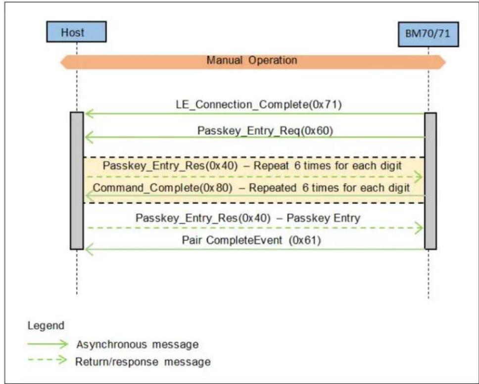
flowchart
sequenceDiagram
    A["Host"] -->|Manual Operation| B["BM70/71"]
    B -->|Passkey_Entry_Req(0x60)| C["LE_Connection_Complete(0x71)"]
    C -->|Passkey_Entry_Res(0x40) – Repeat 6 times for each digit| D["Command_Complete(0x80) – Repeated 6 times for each digit"]
    D -->|Passkey_Entry_Res(0x40) – Passkey Entry| E["Pair CompleteEvent (0x61)"]
    E -->|Passkey_Entry_Req(0x60)| C
    style A fill:#99CCFF,stroke:#333
    style B fill:#99CCFF,stroke:#333
    style C fill:#99CCFF,stroke:#333
    style D fill:#99CCFF,stroke:#333
    style E fill:#99CCFF,stroke:#333
2.3.3.45.4 Applicable Configuration
This event is available in both Auto Operation and Manual Operation.
2.3.3.46 PAIRING - PASSKEY CONFIRM REQUEST EVENT
(OPCODE - 0X62)
This event is sent by the BM70/71 module to inform the host that the passkey received needs to confirmed. The host will reply with the Passkey Confirm Response (0x41) command.
2.3.3.46.1 Event Format, BM70/71 Module to Host
Table 2-108 provides details of the event format from the BM70/71 module to the host.
TABLE 2-108: EVENT FORMAT, BM70/71 MODULE TO HOST
| Start Length (H) Length (L) OP Code Parameter Checksum | ||||||
| Byte No 0 1 2 | 3 | 4 to 10 | 5 | |||
| Value | 0xAA | 0x00 | 0x08 | 0x62 | see Table 2-109 | value |
Table 2-109 provides the parameter values and lengths.
TABLE 2-109: PARAMETER VALUES AND LENGTHS
| Value of Parameter | Parameter Description | Length |
| Value of Parameter (4) | ||
| 0xXX | Connection handle of current connection. This value was returned by the BM70/71 module in an LE Connect Complete Event (0x71) response. | 1 byte |
| Value of Parameter (5 to 10) | ||
| 0xXX | Each digit of the six-digit passkey is represented in ASCII | 6 bytes |
2.3.3.46.2 Default
This does not apply to this event.
2.3.3.46.3 Example
Figure 2-51 illustrates an example of the passkey confirm request event from the BM70/71 module to the host.
FIGURE 2-51: SEQUENCE DIAGRAM OF PAIRING - PASSKEY CONFIRM REQUEST EVENT

flowchart
sequenceDiagram
    A["Host"] -->|Passkey Confirm Request Event (0x62)| B["BM70/71"]
    B -->|Passkey Confirm Response (0x41)| A
    A -->|Passkey Confirm Response (0x62)| B
    B -->|Passkey Confirm Response (0x41)| A
    A -->|Pairing Complete Event (0x61)| B
    B -->|Pairing Complete Event (0x61)| A
    A -->|Status Report Event (0x81)| B
    B -->|Status Report Event (0x81)| A
    A -->|Ready to receive command| B
2.3.3.46.4 Applicable Configuration
This event is available in both Manual Operation and Auto Operation.
2.3.3.47 ADVERTISING REPORT EVENT (OPCODE - 0X70)
This event is sent by the BM70/71 module to inform the host that another Bluetooth Low Energy device has responded to an active/passive scan.
2.3.3.47.1 Event Format, BM70/71 Module to Host
Table 2-110 provides details of the event format from the BM70/71 module to the host.
TABLE 2-110: EVENT FORMAT, BM70/71 MODULE TO HOST
| Start Length (H) Length (L) OP Code Parameter Checksum | ||||||
| Byte No | 0 | 1 | 2 | 3 | 4 to x | 5 |
| Value | 0xAA | 0x00 | 0x0B - 0xNN | 0x70 | see Table 2-111 | value |
Table 2-111 provides the parameter values and lengths.
TABLE 2-111: PARAMETER VALUES AND LENGTHS
| Value of Parameter | Parameter Description | Length |
| Value of Parameter (4) | ||
| 0x00 | A connectable undirected advertising packet was received | 1 byte |
| 0x01 | A connectable directed advertising packet was received | |
| 0x02 | A scanable undirected advertising packet was received | |
| 0x03 | A non-connectable undirected advertising packet was received | |
| 0x04 | A scan response packet was received | |
| Value of Parameter (5) | ||
| 0x00 | Public Device Address | 1 byte |
| 0x01 | Random device address | |
| Value of Parameter (6 to 11) | ||
| 0xXXXX_XXXX_XXXX | Bluetooth address of device | 6 bytes |
| Value of Parameter (12) | ||
| 0xXX | Length of data payload from packet | 1 byte |
| Value of Parameter (13 to n) | ||
| 0xXX | Data received in advertising or scan response packet | 1 to 31 bytes (max) |
| Value of Parameter (x) | ||
| 0xXX | Signed digital value representing RSSI (dBm) from remote device sending packet. A value of -127 or 0x81 means RSSI was not available. | 1 byte |
2.3.3.47.2 Default
This does not apply to this event.
2.3.3.47.3 Example
Figure 2-52 illustrates an example of the advertising report event from the BM70/71 module to the host.
FIGURE 2-52: SEQUENCE DIAGRAM OF ADVERTISING REPORT EVENT

flowchart
graph TD
    A["Host"] -->|Set Scan Enable (0x16)| B["BM70/71"]
    B -->|Command Complete Event (0x80)| A
    A -->|Status Report Event (0x81)| B
    B -->|Scanning mode| A
    A -->|Advertising Report Event (0x70)| B
    style A fill:#99CCFF
    style B fill:#99CCFF
    note1["Legend: Asynchronous message"] --> A
    note2["Return/response message"] --> B
2.3.3.47.4 Applicable Configuration
This event is only available in Manual Operation.
2.3.3.48 LE CONNECTION COMPLETE EVENT (OPCODE - 0X71)
The BM70/71 module returns an LE Connection Complete Event(0x71) response to the host when a connection with a peer device is attempted. This command indicates if the execution was successful or not. If successful, the parameters associated with the connected peer device are returned.
2.3.3.48.1 Event Format, BM70/71 Module to Host
Table 2-112 provides details of the event format from the BM70/71 module to the host.
TABLE 2-112: EVENT FORMAT, BM70/71 MODULE TO HOST
| Start Length (H) Length (L) OP Code Parameter Checksum | ||||||
| Byte No 0 1 2 | 3 | 4 to 19 | 5 | |||
| Value | 0xAA | 0x00 | 0x10 | 0x71 | see Table 2-113 | value |
Table 2-113 provides the parameter values and lengths.
TABLE 2-113: PARAMETER VALUES AND LENGTHS
| Value of Parameter | Parameter Description | Length |
| Value of Parameter (4) | ||
| 0x00 | Connection successfully completed | 1 byte |
| 0x01 to 0xFF | Connection failed to complete | |
| Value of Parameter (5) | ||
| 0xXX | Connection Handle to be used to identify a connection between the BM70/71 module and the peer device | 1 byte |
| Value of Parameter (6) | ||
| 0x00 | BM70/71 module is the master in the connection | 1 byte |
| 0X01 | BM70/71 module is the slave in the connection | |
| Value of Parameter (7) | ||
| 0x00 | Peer device is using a public device address | 1 byte |
| 0x01 | Peer is using a Random device address | |
| 0x02 | Peer is a previously bonded device | |
| Value of Parameter (8 to 13) | ||
| 0xXX XX XX XX XX XX | Peer device Bluetooth address | 6 bytes |
| Value of Parameter (14 to 15) | ||
| 0xXXXX | Connection Interval used for this connectionRange: 0x0006 (7.5 ms) - 0x0C80 (4s)Interval = value * 1.25 msParameter 14 is MSBParameter 15 is LSB | 2 bytes |
| Value of Parameter (16 to 17) | ||
| 0xXXXX | Slave Latency is the number of connection events a slave can miss before the connection is considered lostRange: 0x0000 (0 connection events) - 0x01F4 (500 connection events)Parameter 16 is MSBParameter 17 is LSB | 2 bytes |
| Value of Parameter (18 to 19) | ||
TABLE 2-113: PARAMETER VALUES AND LENGTHS
| Value of Parameter Parameter Description Length | ||
| 0xXXXX Supervision timeout | it is the maximum amount of time allowed between two packets being received. If this timeout is exceeded and two or more packets have not been received, the connection is considered lost.Range: 0x0006 (7.5 ms) - 0x0C80 (4s)Timeout = value * 1.25 msParameter 18 is MSBParameter 19 is LSB | 2 bytes |
2.3.3.48.2 Default
This does not apply for this event.
2.3.3.48.3 Example
Figure 2-53 and Figure 2-54 illustrate examples of the LE Connection complete event from the BM70/71 module to the host. Note that the Connection complete event (0x71) will be preceded by the relevant Status report event (0x81) message from the BM70/71 module.
FIGURE 2-53: SEQUENCE DIAGRAM OF CONNECTION COMPLETE EVENT-EXAMPLE 1

flowchart
graph LR
    A["Host"] -->|Asynchronous message| B["BM70/71"]
    B -->|Return/response message| A
    style A fill:#99ccff,stroke:#333
    style B fill:#99ccff,stroke:#333
    linkStyle 0 stroke:#000,stroke-width:2px
    linkStyle 1 stroke:#000,stroke-width:2px
    linkStyle 2 stroke:#000,stroke-width:2px
    linkStyle 3 stroke:#000,stroke-width:2px
    linkStyle 4 stroke:#000,stroke-width:2px
    linkStyle 5 stroke:#000,stroke-width:2px
    linkStyle 6 stroke:#000,stroke-width:2px
    linkStyle 7 stroke:#000,stroke-width:2px
    linkStyle 8 stroke:#000,stroke-width:2px
    linkStyle 9 stroke:#000,stroke-width:2px
    linkStyle 10 stroke:#000,stroke-width:2px
    linkStyle 11 stroke:#000,stroke-width:2px
    linkStyle 12 stroke:#000,stroke-width:2px
    linkStyle 13 stroke:#000,stroke-width:2px
    linkStyle 14 stroke:#000,stroke-width:2px
    linkStyle 15 stroke:#000,stroke-width:2px
    linkStyle 16 stroke:#000,stroke-width:2px
    linkStyle 17 stroke:#000,stroke-width:2px
    linkStyle 18 stroke:#000,stroke-width:2px
    linkStyle 19 stroke:#000,stroke-width:2px
    linkStyle 20 stroke:#000,stroke-width:2px
    linkStyle 21 stroke:#000,stroke-width:2px
    linkStyle 22 stroke:#000,stroke-width:2px
    linkStyle 23 stroke:#000,stroke-width:2px
    linkStyle 24 stroke:#000,stroke-width:2px
    linkStyle 25 stroke:#000,stroke-width:2px
    linkStyle 26 stroke:#000,stroke-width:2px
    linkStyle 27 stroke:#000,stroke-width:2px
    linkStyle 28 stroke:#000,stroke-width:2px
    linkStyle 29 stroke:#000,stroke-width:2px
    linkStyle 30 stroke:#000,stroke-width:2px
    linkStyle 31 stroke:#000,stroke-width:2px
    linkStyle 32 stroke:#000,stroke-width:2px
    linkStyle 33 stroke:#000,stroke-width:2px
    linkStyle 34 stroke:#000,stroke-width:2px
    linkStyle 35 stroke:#000,stroke-width:2px
    linkStyle 36 stroke:#000,stroke-width:2px
    linkStyle 37 stroke:#000,stroke-width:2px
    linkStyle 38 stroke:#000,stroke-width:2px
    linkStyle 39 stroke:#000,stroke-width:2px
    linkStyle 40 stroke:#000,stroke-width:2px
    linkStyle 41 stroke:#000,stroke-width:2px
    linkStyle 42 stroke:#000,stroke-width:2px
    linkStyle 43 stroke:#000,stroke-width:2px
    linkStyle 44 stroke:#000,stroke-width:2px
    linkStyle 45 stroke:#999999,stroke-width:1px
FIGURE 2-54: SEQUENCE DIAGRAM OF CONNECTION COMPLETE EVENT-EXAMPLE 2

flowchart
graph TD
    A["Host"] -->|Connection Complete Event (0x71)| B["BM70/71"]
    B -->|Ready to receive command| A
    style A fill:#4CAF50,stroke:#388E3C
    style B fill:#4CAF50,stroke:#388E3C
    note right of A: Legend → Asynchronous message
2.3.3.48.4 Applicable Configuration
This event is only available in Manual Operation.
2.3.3.49 DISCONNECT COMPLETE EVENT (OPCODE - 0X72)
This event response is sent by the BM70/71 module to the host after a connection is terminated. The role (central/master or peripheral/slave) of the BM70/71 module is not considered when the connection is dropped. This event response indicates the reason the connection was terminated in the parameters field.
2.3.3.49.1 Event Format, BM70/71 Module to Host
Table 2-114 provides details of the event format from the BM70/71 module to the host.
TABLE 2-114: EVENT FORMAT, BM70/71 MODULE TO HOST
| Start Length (H) Length (L) OP Code Parameter Checksum | ||||||
| Byte No 0 1 2 | 3 | 4 to 5 | 5 | |||
| Value | 0xAA | 0x00 | 0x03 | 0x72 | see Table 2-115 | value |
Table 2-115 provides the parameter values and lengths.
TABLE 2-115: PARAMETER VALUES AND LENGTHS
| Value of Parameter | Parameter Description | Length |
| Value of Parameter (4) | ||
| 0xXX | Connection handleThis is the value sent to the host by the BM70/71 module in an LE Connection Complete Event(0x71) | 1 byte |
| Value of Parameter (5) | ||
| 0x08 | Connection Timeout | 1 byte |
| 0X09 | Connection limit exceeded | |
| 0x0B | ACL connection already exists | |
| 0x0D | Connection rejected due to limited resources | |
| 0x0E | Connection rejected due to security reasons | |
| 0x0F | Connection rejected due to unacceptable BD_ADDR | |
| 0x10 | Connection accept Timeout exceeded | |
| 0x11 | Unsupported feature or Parameter value | |
| 0x12 | Invalid command parameters | |
| 0x13 | Remote user terminated connection | |
| 0x14 | Remote device terminated connection due to low resources | |
| 0x15 | Remote device terminated connection due to power off | |
| 0x16 | Connection terminated by local host | |
| 0x1F | Unspecified error | |
| 0x39 | Connection rejected due to no suitable channel found | |
| 0x3A | Controller busy | |
| 0x3D | Connection terminated due to MIC failure | |
| 0x3E | Connection failed to establish | |
| 0x84 | Invalid PDU | |
| 0x91 | Insufficient Resources | |
2.3.3.49.2 Default
This does not apply to this event.
2.3.3.49.3 Example
Figure 2-55 and Figure 2-56 illustrate examples of the disconnect complete event from the BM70/71 module to the host.
FIGURE 2-55: SEQUENCE DIAGRAM OF DISCONNECT COMPLETE EVENT-EXAMPLE 1
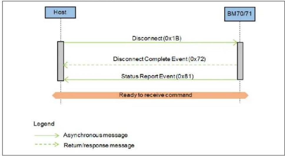
flowchart
graph LR
    A["Host"] -->|Disconnect(0x1B)| B["BM70/71"]
    B -->|Disconnect Complete Event (0x72)| A
    A -->|Status Report Event (0x81)| B
    B -->|Ready to receive command| A
    style A fill:#99CCFF,stroke:#333
    style B fill:#99CCFF,stroke:#333
    note right of A: Legend
    linkStyle 0 stroke:#000,stroke-width:2px
    linkStyle 1 stroke:#000,stroke-width:2px
    linkStyle 2 stroke:#000,stroke-width:2px
    linkStyle 3 stroke:#000,stroke-width:2px
    linkStyle 4 stroke:#000,stroke-width:2px
    linkStyle 5 stroke:#000,stroke-width:2px
    linkStyle 6 stroke:#000,stroke-width:2px
    linkStyle 7 stroke:#000,stroke-width:2px
    linkStyle 8 stroke:#000,stroke-width:2px
    linkStyle 9 stroke:#000,stroke-width:2px
    linkStyle 10 stroke:#000,stroke-width:2px
    linkStyle 11 stroke:#000,stroke-width:2px
    linkStyle 12 stroke:#000,stroke-width:2px
    linkStyle 13 stroke:#000,stroke-width:2px
    linkStyle 14 stroke:#000,stroke-width:2px
    linkStyle 15 stroke:#000,stroke-width:2px
    linkStyle 16 stroke:#000,stroke-width:2px
    linkStyle 17 stroke:#000,stroke-width:2px
    linkStyle 18 stroke:#000,stroke-width:2px
    linkStyle 19 stroke:#000,stroke-width:2px
    linkStyle 20 stroke:#000,stroke-width:2px
FIGURE 2-56: SEQUENCE DIAGRAM OF DISCONNECT COMPLETE EVENT-EXAMPLE 2
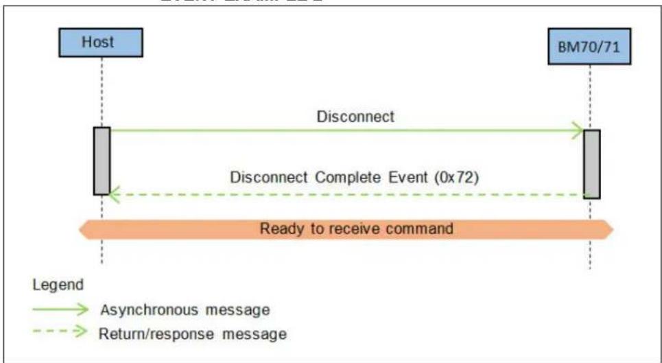
flowchart
graph LR
    A["Host"] -->|Disconnect| B["BM70/71"]
    B -->|Disconnect Complete Event (0x72)| A
    style A fill:#4CAF50,stroke:#388E3C
    style B fill:#4CAF50,stroke:#388E3C
    note right of B: Ready to receive command
    note left of B: Asynchronous message
    note right of B: Return/response message
2.3.3.49.4 Applicable Configuration
This event is only available in Manual Operation.
2.3.3.50 CONNECTION PARAMETER UPDATE EVENT (OPCODE - 0x73)
This event is sent by the BM70/71 module to inform the host that the connection parameters have changed.
2.3.3.50.1 Event Format, BM70/71 Module to Host
Table 2-116 provides details of the event format from the BM70/71 module to the host.
TABLE 2-116: EVENT FORMAT, BM70/71 MODULE TO HOST
| Start Length (H) Length (L) OP Code Parameter Checksum | ||||||
| Byte No 0 1 2 | 3 | 4 to 5 | 5 | |||
| Value | 0xAA | 0x00 | 0x03 | 0x73 | see Table 2-117 | value |
Table 2-117 provides the parameter values and lengths.
TABLE 2-117: PARAMETER VALUES AND LENGTHS
| Value of Parameter | Parameter Description | Length |
| Value of Parameter (4) | ||
| 0xXX | Connection handleThis is the value sent to the host by the BM70/71 module in an LE Connection Complete Event (0x71) | 1 byte |
| Value of Parameter (5 to 6) | ||
| 0xXXXX | Connection Event intervalInterval = x * 1.25 ms | 2 bytes |
| Value of Parameter (7 to 8) | ||
| 0xXXXX | Slave Latency. This is the number of connection events which the slave can miss before the connection is considered lost.Range: 0x0000 - 0x01F4 | 2 bytes |
| Value of Parameter (9 to 10) | ||
| 0xXXXX | Supervision TimeoutRange: 0x000A - 0x0C80Timeout = x * 10 ms | 2 bytes |
2.3.3.50.2 Default
This does not apply to this event.
2.3.3.50.3 Example
If the BM70/71 module has the role of a slave in the connection, the host can request the connection parameters to be updated, but it is up to the peer device (master) to determine if this will occur. When a Connection Parameter Update Request (0x19) command is sent by the host, the BM70/71 module returns the Command Complete Event (0x80) response to let the host know the request was successful. The BM70/71 module returns the Connection Parameter Update Event (0x73) when the connection parameters have been updated.
Figure 2-45 illustrates an example of the connection parameter update request from the BM70/71 module to the host.
FIGURE 2-57: SEQUENCE DIAGRAM OF CONNECTION PARAMETER UPDATE

flowchart
graph TD
    A["Host"] --> B["BM70/71"]
    B --> C["Connection Parameter Update Event (0x73)"]
    C --> D["Command Complete Event (0x80)"]
    D --> E["Connection Parameter Update Request (0x19)"]
    E --> F["Ready to receive command"]
    F --> G["Legend"]
    style A fill:#4CAF50,stroke:#333
    style B fill:#4CAF50,stroke:#333
    style C fill:#4CAF50,stroke:#333
    style D fill:#4CAF50,stroke:#333
    style E fill:#4CAF50,stroke:#333
    style F fill:#FFA500,stroke:#333
    style G fill:#FFA500,stroke:#333
2.3.3.50.4 Applicable Configuration
This event is only available in Manual Operation.
2.3.3.51 COMMAND COMPLETE EVENT (OPCODE - 0X80)
This event is sent by the BM70/71 module to the host when a host command message is received and executed successfully. The BM70/71 module can also send this event message when it has processed a Bluetooth Low Energy-related mode or procedure. This event message has a general format and is based on the specific host command or Bluetooth Low Energy mode/procedure. Additional information will be added to inform the host of the processing status. Not all host command messages or Bluetooth Low Energy modes/procedures executed will add additional information. The host must be capable of processing this event message in both cases.
2.3.3.51.1 Event Format, BM70/71 Module to Host
Table 2-118 provides details of the event format from the BM70/71 module to the host.
TABLE 2-118: EVENT FORMAT, BM70/71 MODULE TO HOST
| Start Length (H) | Length (L) | Event OP Code | Command OP Code | Command Status | Parameter | Checksum | |
| Byte No 0 | 2 3 4 5 6 to n | n+1 | |||||
| Value | 0xAA | 0x00 | 0xXX | 0x80 | 0xXX | 0xXX | Command response data |
Table 2-119 provides the details of the Command Complete Event(0x80) parameter values and lengths.
TABLE 2-119: PARAMETER VALUES AND LENGTHS
| Value of Parameter (4) | Parameter Description Length | |
| 0x00 Command | succeeded 1 byte | |
| 0x01 Unknown | command | |
| 0x02 Unknown | connection identifier | |
| 0x03 Hardware | failure | |
| 0x05 Authentication failure | ||
| 0x06 PIN or Key missing | ||
| 0x07 Memory capacity exceeded | ||
| 0x08 Connection timeout | ||
| 0x09 Connection limit exceeded | ||
| 0x0B ACL connection already exists | ||
| 0x0C Command disallowed | ||
| 0x0D Connection rejected due to limited resources | ||
| 0x0E Connection rejected due to Security reasons | ||
| 0x0F Connection rejected due to Unacceptable BD_ADDR | ||
| 0x10 Connection accept timeout exceeded | ||
| 0x11 Unsupported feature or Parameter value | ||
| 0x12 Invalid command parameters | ||
| 0x13 Remote user terminated connection | ||
| 0x14 Remote device terminated connection due to low resources | ||
| 0x15 Remote device terminated connection due to Power Off | ||
| 0x16 Connection terminated by local Host | ||
| 0x18 Pairing not allowed | ||
| 0x1F Unspecified error | ||
| 0x28 Instant passed | ||
| 0x29 Pairing with Unit Key not supported | ||
| 0x2F Insufficient Security | ||
| 0x39 Connection rejected due to no suitable channel found | ||
| 0x3A Controller busy | ||
| 0x3B Unacceptable connection interval | ||
| 0x3C Directed Advertising timeout | ||
| 0x3D Connection terminated due to MIC failure | ||
| 0x3E Connection failed to be established | ||
| 0x77 Invalid Offset | ||
| 0x81 Invalid Handle | ||
| 0x82 Read not permitted | ||
| 0x83 Write not permitted | ||
| 0x84 Invalid PDU | ||
| 0x85 Insufficient Authentication | ||
| 0x86 Request not supported | ||
| 0x88 Insufficient Authorization | ||
| 0x89 Prepare queue full | ||
| 0x8A Attribute not found | ||
| 0x8B Attribute not long | ||
| 0x8C Insufficient encryption Key size | ||
| 0x8D Invalid Attribute value length | ||
| 0x8E Unlikely error | ||
| 0x8F Insufficient encryption | ||
| 0x90 Unsupported Group type | ||
| 0x91 Insufficient Resources | ||
| 0xF0 Application defined error | ||
| 0xFF UART Checksum error | ||
2.3.3.51.2 Default
This does not apply to this event.
2.3.3.51.3 Example
Figure 2-58 illustrates an example of the complete command event from the BM70/71 module to the host.
FIGURE 2-58: SEQUENCE DIAGRAM OF COMMAND COMPLETE EVENT

flowchart
graph LR
    A["Host"] -->|Asynchronous| B["BM70/71"]
    B -->|Return/response| A
    style A fill:#99ccff,stroke:#333
    style B fill:#99ccff,stroke:#333
    note right of A: "Command Complete Event (0x80)"
    note right of B: "Ready to receive command"
    note left of A: "Host Command"
2.3.3.51.4 Applicable Configuration
This event can be sent in Manual Operation or in Auto Operation only when the "Configuration Window" is active.
2.3.3.52 STATUS REPORT EVENT (OPCODE - 0X81)
The BM70/71 module will respond to commands that cause a mode change or want to know state with a Status Report Event(0x81) response. The value in the parameter field will indicate the mode (temporary sub-state) the BM70/71 module is in. There is a total of nine modes that the BM70/71 module can be in. Not all modes apply to all states within the BM70/71 module.
2.3.3.52.1 Event Format, BM70/71 Module to Host
Table 2-120 provides details of the event format from the BM70/71 module to the host.
TABLE 2-120: EVENT FORMAT, BM70/71 MODULE TO HOST
| Start Length (H) | Length (L) | OP Code | Parameter | Checksum | ||
| Byte No | 0 | 1 | 2 | 3 | 4 | 5 |
| Value | 0xAA | 0x00 | 0x02 | 0x81 | see Table 2-121 | value |
Table 2-121 provides the parameter values and lengths.
TABLE 2-121: PARAMETER VALUES AND LENGTHS
| Value of Parameter | Parameter Description | Length |
| 0x01 | Scanning mode | 1 byte |
| 0x02 | Connecting mode | |
| 0x03 | Standby mode | |
| 0x05 | Broadcast mode | |
| 0x08 | Transparent Service enabled mode | |
| 0x09 | Idle mode | |
| 0x0A | Shutdown mode | |
| 0x0B | Configure mode | |
| 0x0C | Bluetooth Low Energy Connected mode |
2.3.3.52.2 Default
This does not apply to this event.
2.3.3.52.3 Example
Figure 2-59 and Figure 2-60 illustrate two examples of how the Status Report Event(0x81) response is sent by the BM70/71 module to the host.
FIGURE 2-59: SEQUENCE DIAGRAM OF STATUS REPORT
EVENT-EXAMPLE 1

flowchart
graph TD
    A["Host"] -->|Asynchronous| B["BM70/71"]
    B -->|Return/response| A
    style A fill:#99ccff,stroke:#333
    style B fill:#99ccff,stroke:#333
    linkStyle 0 stroke:#000,stroke-width:2px
    linkStyle 1 stroke:#000,stroke-width:2px
    linkStyle 2 stroke:#000,stroke-width:2px
    linkStyle 3 stroke:#000,stroke-width:2px
    linkStyle 4 stroke:#000,stroke-width:2px
    linkStyle 5 stroke:#000,stroke-width:2px
    linkStyle 6 stroke:#000,stroke-width:2px
    linkStyle 7 stroke:#000,stroke-width:2px
    linkStyle 8 stroke:#000,stroke-width:2px
    linkStyle 9 stroke:#000,stroke-width:2px
    linkStyle 10 stroke:#000,stroke-width:2px
    linkStyle 11 stroke:#000,stroke-width:2px
    linkStyle 12 stroke:#000,stroke-width:2px
    linkStyle 13 stroke:#000,stroke-width:2px
    linkStyle 14 stroke:#000,stroke-width:2px
    linkStyle 15 stroke:#000,stroke-width:2px
    linkStyle 16 stroke:#000,stroke-width:2px
    linkStyle 17 stroke:#000,stroke-width:2px
    linkStyle 18 stroke:#000,stroke-width:2px
    linkStyle 19 stroke:#000,stroke-width:2px
    linkStyle 20 stroke:#000,stroke-width:2px
    linkStyle 21 stroke:#000,stroke-width:2px
    linkStyle 22 stroke:#000,stroke-width:2px
    linkStyle 23 stroke:#000,stroke-width:2px
    linkStyle 24 stroke:#000,stroke-width:2px
    linkStyle 25 stroke:#000,stroke-width:2px
    linkStyle 26 stroke:#000,stroke-width:2px
    linkStyle 27 stroke:#000,stroke-width:2px
    linkStyle 28 stroke:#000,stroke-width:2px
    linkStyle 29 stroke:#000,stroke-width:2px
    linkStyle 30 stroke:#000,stroke-width:2px
    linkStyle 31 stroke:#000,stroke-width:2px
    linkStyle 32 stroke:#000,stroke-width:2px
    linkStyle 33 stroke:#000,stroke-width:2px
    linkStyle 34 stroke:#000,stroke-width:2px
    linkStyle 35 stroke:#000,stroke-width:2px
    linkStyle 36 stroke:#000,stroke-width:2px
    linkStyle 37 stroke:#000,stroke-width:2px
    linkStyle 38 stroke:#000,stroke-width:2px
    linkStyle 39 stroke:#000,stroke-width:2px
    linkStyle 40 stroke:#000,stroke-width:2px
    linkStyle 41 stroke:#000,stroke-width:2px
    linkStyle 42 stroke:#000,stroke-width:2px
    linkStyle 43 stroke:#000,stroke-width:2px
    linkStyle 44 stroke:#000,stroke-width:2px
    linkStyle 45 stroke:#999999,stroke-width:1px
FIGURE 2-60: SEQUENCE DIAGRAM OF STATUS REPORT
EVENT-EXAMPLE 2

flowchart
graph TD
    A["Host"] -->|Host command| B["BM70/71"]
    B -->|Command Complete Event (0x80)| A
    B -->|Status Report Event (0x81)| A
    A -->|Ready to receive new commands| B
    style A fill:#99ccff,stroke:#333
    style B fill:#99ccff,stroke:#333
    note right of A: Legend: Asynchronous → Return/response
2.3.3.52.4 Applicable Configuration
This event is only available in Manual Operation.
2.3.3.53 CONFIGURE MODE STATUS EVENT (OPCODE - 0X8F)
This event is sent by the BM70/71 module to inform the host of the “Configuration Window” status during Auto Operation.
2.3.3.53.1 Event Format, BM70/71 Module to Host
Table 2-122 provides details of the event format from the BM70/71 module to the host.
TABLE 2-122: EVENT FORMAT, BM70/71 MODULE TO HOST
| Start Length (H) | Length (L) | OP Code | Parameter | Checksum | ||
| Byte No | 0 | 1 | 2 | 3 | 4 | 5 |
| Value | 0xAA | 0x00 | 0x02 | 0x8F | see Table 2-123 | value |
Table 2-123 provides the parameter values and lengths.
TABLE 2-123: PARAMETER VALUES AND LENGTHS
| Value of Parameter | Parameter Description | Length |
| 0x00 | Configure mode is disabled | 1 byte |
| 0x01 | Configure mode is enabled |
2.3.3.53.2 Default
This does not apply to this event.
2.3.3.53.3 Example
Figure 2-61 illustrates an example of the configure mode status event sent by the BM70/71 module to the host.
FIGURE 2-61: SEQUENCE DIAGRAM OF CONFIGURE MODE STATUS EVENT
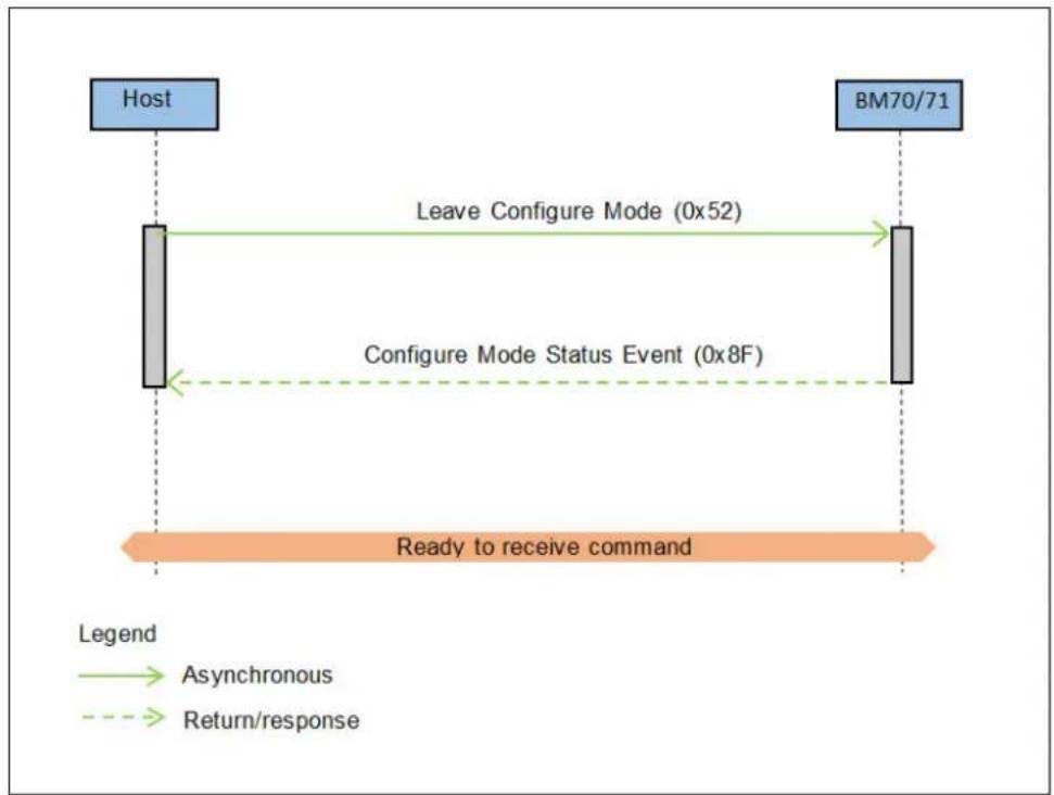
flowchart
graph TD
    A["Host"] -->|Leave Configure Mode (0x52)| B["BM70/71"]
    B -->|Configure Mode Status Event (0x8F)| A
    A -->|Ready to receive command| C["Orange Message"]
    style A fill:#99CCFF,stroke:#333
    style B fill:#99CCFF,stroke:#333
    style C fill:#FFD700,stroke:#333
2.3.3.53.4 Applicable Configuration
This event is only available in Auto Operation.
2.3.3.54 DISCOVER ALL PRIMARY SERVICES EVENT (OPCODE - 0X90)
This event is sent by the BM70/71 module to inform the host of all primary services within the service table of the module.
2.3.3.54.1 Event Format, BM70/71 Module to Host
Table 2-124 provides details of the event format from the BM70/71 module to the host.
TABLE 2-124: EVENT FORMAT, BM70/71 MODULE TO HOST
| Start Length (H) Length (L) OP Code Parameter Checksum | ||||||
| Byte No 0 1 2 | 3 | 4 to n | 5 | |||
| Value | 0xAA | 0x00 | 0xNN | 0x90 | see Table 2-125 | value |
Table 2-125 provides the parameter values and lengths.
TABLE 2-125: PARAMETER VALUES AND LENGTHS
| Value of Parameter | Parameter Description | Length |
| Value of Parameter (4) | ||
| 0x00 | Connection handleThis is the value sent to the host by the BM70/71 module in an LE Connection Complete Event (0x71) | 1 byte |
| Value of Parameter (5) | ||
| 0xXX | The length of each block of information for the primary services which follow.The number of blocks can be inferred by the length of this event packet. There can be multiple blocks included in one event response. The data shown in parameters 6 to 25 may be repeated based on the number of primary services available. | 1 byte |
| Value of Parameter (6 to 7) | ||
| 0xXXXX | Start group handle of the service definition (formatted in little endian) | 2 bytes |
| Value of Parameter (8 to 9) | ||
| 0xXXXX | End group handle of the service definition (formatted in little endian) | 2 bytes |
| Value of Parameter (10 to 11) or (10 to 25) | ||
| 0xXXXXor0xXXXX_XXXX_XXXX-XXXXXXXXX_XXXX-XXXX_XXXX | 16-bit or 128-bit service UUID (formatted as little endian) | 2 bytes or 16 bytes |
2.3.3.54.2 Default
This does not apply to this event.
2.3.3.54.3 Example
Figure 2-62 illustrates an example of the discover all primary services event from the BM70/71 module to the host.
FIGURE 2-62: SEQUENCE DIAGRAM OF DISCOVER ALL PRIMARY SERVICES

flowchart
graph TD
    A["Host"] -->|Read All Local Primary Services (0x3B)| B["BM70/71"]
    B -->|Discover All Primary Services Event Response Event (0x90)| A
    A -->|Command Complete Event (0x80)| B
    B -->|Ready to receive command| A
    style A fill:#4CAF50,stroke:#333
    style B fill:#4CAF50,stroke:#333
    linkStyle 0 stroke:#FFA500,stroke-width:2px
    linkStyle 1 stroke:#FFA500,stroke-width:2px
    linkStyle 2 stroke:#FFA500,stroke-width:2px
    linkStyle 3 stroke:#FFA500,stroke-width:2px
    linkStyle 4 stroke:#FFA500,stroke-width:2px
    linkStyle 5 stroke:#FFA500,stroke-width:2px
    linkStyle 6 stroke:#FFA500,stroke-width:2px
    linkStyle 7 stroke:#FFA500,stroke-width:2px
    linkStyle 8 stroke:#FFA500,stroke-width:2px
    linkStyle 9 stroke:#FFA500,stroke-width:2px
    linkStyle 10 stroke:#FFA500,stroke-width:2px
    linkStyle 11 stroke:#FFA500,stroke-width:2px
    linkStyle 12 stroke:#FFA500,stroke-width:2px
    linkStyle 13 stroke:#FFA500,stroke-width:2px
    linkStyle 14 stroke:#FFA500,stroke-width:2px
    linkStyle 15 stroke:#FFA500,stroke-width:2px
    linkStyle 16 stroke:#FFA500,stroke-width:2px
    linkStyle 17 stroke:#FFA500,stroke-width:2px
    linkStyle 18 stroke:#FFA500,stroke-width:2px
    linkStyle 19 stroke:#FFA500,stroke-width:2px
    linkStyle 20 stroke:#FFA500,stroke-width:2px
    linkStyle 21 stroke:#FFA500,stroke-width:2px
    linkStyle 22 stroke:#FFA500,stroke-width:2px
    linkStyle 23 stroke:#FFA500,stroke-width:2px
    linkStyle 24 stroke:#FFA500,stroke-width:2px
    linkStyle 25 stroke:#FFA500,stroke-width:2px
    linkStyle 26 stroke:#FFA500,stroke-width:2px
    linkStyle 27 stroke:#FFA500,stroke-width:2px
    linkStyle 28 stroke:#FFA500,stroke-width:2px
    linkStyle 29 stroke:#FFA500,stroke-width:2px
    linkStyle 30 stroke:#FFA500,stroke-width:2px
    linkStyle 31 stroke:#FFA500,stroke-width:2px
    linkStyle 32 stroke:#FFA500,stroke-width:2px
    linkStyle 33 stroke:#FFA500,stroke-width:2px
    linkStyle 34 stroke:#FFA500,stroke-width:2px
    linkStyle 35 stroke:#FFA500,stroke-width:2px
    linkStyle 36 stroke:#FFA500,stroke-width:2px
    linkStyle 37 stroke:#FFA500,stroke-width:2px
    linkStyle 38 stroke:#FFA500,stroke-width:2px
    linkStyle 39 stroke:#FFA500,stroke-width:2px
    linkStyle 40 stroke:#FFA500,stroke-width:2px
    linkStyle 41 stroke:#FFA500,stroke-width:2px
    linkStyle 42 stroke:#FFA500,stroke-width:2px
    linkStyle 43 stroke:#FFA500,stroke-width:2px
    linkStyle 44 stroke:#FFA500,stroke-width:2px
    linkStyle 45 stroke:#FFA500,stroke-width:2px
    linkStyle 46 stroke:#FFA500,stroke-width:2px
    linkStyle 47 stroke:#FFA500,stroke-width:2px
    linkStyle 48 stroke:#FFA500,stroke-width:2px
    linkStyle 49 stroke:#FFA500,stroke-width:2px
    linkStyle 50 stroke:#FFA500,stroke-width:2px
2.3.3.54.4 Applicable Configuration
This event is only available in Manual Operation.
2.3.3.55 DISCOVER SPECIFIC PRIMARY SERVICE
CHARACTERISTIC DECLARATION EVENT (OPCODE - 0X91)
The event is sent by the BM70/71 module to inform the host of the "Characteristic declaration" attribute type. It is possible to have multiple characteristic definitions for a specific primary service. Each characteristic definition has its own characteristic declaration attribute type. In these cases, the BM70/71 module will have to send multiple event responses (0x91) to the host. The host needs to be capable of processing multiple event responses.
Figure 2-63 illustrates the visual structure of the “Characteristic declaration” attribute. The values of each column are returned to the host with this event response.
FIGURE 2-63: CHARACTERISTIC DECLARATION ATTRIBUTE STRUCTURE

flowchart
graph TD
    A["Handle"] --> B["Type"]
    B --> C["Value"]
    C --> D["Permissions"]
    style A fill:#99ccff,stroke:#333
    style B fill:#99ccff,stroke:#333
    style C fill:#99ccff,stroke:#333
    style D fill:#99ccff,stroke:#333
2.3.3.55.1 Event Format, BM70/71 Module to Host
Table 2-126 provides details of the event format from the BM70/71 module to the host.
TABLE 2-126: EVENT FORMAT, BM70/71 MODULE TO HOST
| Start Length (H) | Length (L) | OP Code | Parameter | Checksum | ||
| Byte No | 0 | 1 | 2 | 3 | 4 | 5 |
| Value | 0xAA | 0x00 | 0xXX | 0x91 | see Table 2-127 | value |
Table 2-127 provides the parameter values and lengths.
TABLE 2-127: PARAMETER VALUES AND LENGTHS
| Value of Parameter Parameter | Parameter Description Length | |
| Value of Parameter (4) | ||
| 0xXX Connection handle | This is the value sent to the host by the BM70/71 module in an LE Connection Complete Event (0x71) | 1 byte |
| Value of Parameter (5 to n) | ||
| 0xXX Length of the “Characteristic declaration” attribute. See Figure 2-63 above for maximum length. | (n-5) bytes | |
| Value of Parameter (x to x) | ||
| 0xXXXX Handle “Characteristic declaration” attribute (formatted in little endian) | 2 bytes | |
| Value of Parameter (x) | ||
| 0x01 Broadcast 1 byte | Properties of “Characteristic value” attribute. The property value can have more than one property type. For example, 0x18, will specify, the value field of the “Characteristic value” attribute. It can be written and has the notify ability. | |
| 0x02 Read | ||
| 0x04 Write without Response | ||
| 0x08 Write | ||
| 0x10 Notify | ||
| 0x20 Indicate | ||
| 0x40 Authenticated | ||
| 0x80 Extended Properties | ||
| Value of Parameter (x to x) | ||
| 0xXXXX or 0xXXXX_XXXX_XXXX-XXXX_XXXXXXXX-XXXX_XXXX | 16-bit or 128-bit UUID of “Characteristic value” attribute (formatted as little endian) | 2 to 16 bytes |
2.3.3.55.2 Default
This does not apply to this event.
2.3.3.55.3 Example
Figure 2-64 illustrates an example of the specific primary services event from the BM70/71 module to the host.
FIGURE 2-64: SEQUENCE DIAGRAM OF DISCOVER SPECIFIC PRIMARY SERVICES

flowchart
graph TD
    A["Host"] -->|Host Command| B["BM70/71"]
    B -->|Discover Specific Primary Service Characteristic Declaration Event (0x91)| A
    B -->|Ready to receive command| A
    style A fill:#4CAF50,stroke:#388E3C
    style B fill:#4CAF50,stroke:#388E3C
    linkStyle 0 stroke:#FFA500,stroke-width:2px
    linkStyle 1 stroke:#FFA500,stroke-width:2px
    linkStyle 2 stroke:#FFA500,stroke-width:2px
    linkStyle 3 stroke:#FFA500,stroke-width:2px
    linkStyle 4 stroke:#FFA500,stroke-width:2px
    linkStyle 5 stroke:#FFA500,stroke-width:2px
    linkStyle 6 stroke:#FFA500,stroke-width:2px
    linkStyle 7 stroke:#FFA500,stroke-width:2px
    linkStyle 8 stroke:#FFA500,stroke-width:2px
    linkStyle 9 stroke:#FFA500,stroke-width:2px
    linkStyle 10 stroke:#FFA500,stroke-width:2px
    linkStyle 11 stroke:#FFA500,stroke-width:2px
    linkStyle 12 stroke:#FFA500,stroke-width:2px
    linkStyle 13 stroke:#FFA500,stroke-width:2px
    linkStyle 14 stroke:#FFA500,stroke-width:2px
    linkStyle 15 stroke:#FFA500,stroke-width:2px
    linkStyle 16 stroke:#FFA500,stroke-width:2px
    linkStyle 17 stroke:#FFA500,stroke-width:2px
    linkStyle 18 stroke:#FFA500,stroke-width:2px
    linkStyle 19 stroke:#FFA500,stroke-width:2px
    linkStyle 20 stroke:#FFA500,stroke-width:2px
    linkStyle 21 stroke:#FFA500,stroke-width:2px
    linkStyle 22 stroke:#FFA500,stroke-width:2px
    linkStyle 23 stroke:#FFA500,stroke-width:2px
    linkStyle 24 stroke:#FFA500,stroke-width:2px
    linkStyle 25 stroke:#FFA500,stroke-width:2px
    linkStyle 26 stroke:#FFA500,stroke-width:2px
    linkStyle 27 stroke:#FFA500,stroke-width:2px
    linkStyle 28 stroke:#FFA500,stroke-width:2px
    linkStyle 29 stroke:#FFA500,stroke-width:2px
    linkStyle 30 stroke:#FFA500,stroke-width:2px
    linkStyle 31 stroke:#FFA500,stroke-width:2px
    linkStyle 32 stroke:#FFA500,stroke-width:2px
    linkStyle 33 stroke:#FFA500,stroke-width:2px
    linkStyle 34 stroke:#FFA500,stroke-width:2px
    linkStyle 35 stroke:#FFA500,stroke-width:2px
    linkStyle 36 stroke:#FFA500,stroke-width:2px
    linkStyle 37 stroke:#FFA500,stroke-width:2px
    linkStyle 38 stroke:#FFA500,stroke-width:2px
    linkStyle 39 stroke:#FFA500,stroke-width:2px
    linkStyle 40 stroke:#FFA500,stroke-width:2px
    linkStyle 41 stroke:#FFA500,stroke-width:2px
    linkStyle 42 stroke:#FFA500,stroke-width:2px
    linkStyle 43 stroke:#FFA500,stroke-width:2px
    linkStyle 44 stroke:#FFA500,stroke-width:2px
    linkStyle 45 stroke:#FFA500,stroke-width:2px
    linkStyle 46 stroke:#FFA500,stroke-width:2px
    linkStyle 47 stroke:#FFA500,stroke-width:2px
    linkStyle 48 stroke:#FFA500,stroke-width:2px
    linkStyle 49 stroke:#FFA500,stroke-width:2px
    linkStyle 50 stroke:#FFA500,stroke-width:2px
2.3.3.55.4 Applicable Configuration
This event is only available in Manual Operation.
2.3.3.56 DISCOVER ALL CHARACTERISTIC DESCRIPTORS EVENT (OPCODE - 0X92)
This event is sent by the BM70/71 module to inform the host of the “Characteristic descriptor declaration” attribute UUID(s). There can be several different types of characteristic descriptors used within a characteristic definition. The “Characteristic descriptor” attribute is simply used to provide metadata (additional information about the value in the “Characteristic value” attribute). The representation of this metadata depends on the type of “Characteristic descriptor” attribute used. This can be discovered by referencing the UUID(s) of the “Characteristic descriptor” attribute.
A characteristic definition can have more than one “Characteristic descriptor declaration” attribute. The BM70/71 module will return a UUID for each “Characteristic descriptor declaration” attribute within this event response.
2.3.3.56.1 Event Format, BM70/71 Module to Host
Table 2-128 provides details of the event format from the BM70/71 module to the host.
TABLE 2-128: EVENT FORMAT, BM70/71 MODULE TO HOST
| Start Length (H) Length (L) OP Code Parameter Checksum | ||||||
| Byte No 0 1 2 | 3 | 4 | 5 | |||
| Value | 0xAA | 0x00 | 0x07 to 0x17 | 0x92 | see Table 2-129 | value |
Table 2-129 provides the parameter values and lengths.
TABLE 2-129: PARAMETER VALUES AND LENGTHS
| Value of Parameter | Parameter Description | Length |
| Value of Parameter (4) | ||
| 0xXX | Connection handle | 1 byte |
| Value of Parameter (5) | ||
| 0x01 | This event response lists 16-bit UUID(s) | 1 byte |
| 0x02 | This event response lists 128-bit UUID(s) | |
| Value of Parameter (6 to 7) | ||
| 0xXXXX | Start group handle of the service definition (formatted in little endian) | 2 bytes |
| Value of Parameter (8 to 9) | ||
| 0xXXXX | Handle “Characteristic descriptor declaration” attribute (formatted as little endian) | 2 bytes |
| Value of Parameter (8 to 9) or (8 to 23) | ||
| 0xXXXXor0xXXXX_XXXX_XXXX-_XXXX_XXXXXXXX-_XXXX_XXXX | UUID of “Characteristic descriptor declaration” attribute (formatted as little endian) | 2 bytes or 16 bytes |
2.3.3.56.2 Default
This does not apply to this event.
2.3.3.56.3 Example
Figure 2-65 illustrates an example of the discover all characteristic descriptors event from the BM70/71 module to the host.
FIGURE 2-65: SEQUENCE DIAGRAM OF CHARACTERISTIC DESCRIPTORS

flowchart
graph TD
    A["Host"] -->|Host Command Discover All Characteristic Descriptors Event (0x92)| B["BM70/71"]
    B -->|Ready to receive command| A
    style A fill:#333,stroke:#fff,color:#fff
    style B fill:#333,stroke:#fff,color:#fff
    linkStyle 0 stroke:#000,stroke-width:2px
    linkStyle 1 stroke:#000,stroke-width:2px
    linkStyle 2 stroke:#000,stroke-width:2px
    linkStyle 3 stroke:#000,stroke-width:2px
    linkStyle 4 stroke:#000,stroke-width:2px
    linkStyle 5 stroke:#000,stroke-width:2px
    linkStyle 6 stroke:#000,stroke-width:2px
    linkStyle 7 stroke:#000,stroke-width:2px
    linkStyle 8 stroke:#000,stroke-width:2px
    linkStyle 9 stroke:#000,stroke-width:2px
    linkStyle 10 stroke:#000,stroke-width:2px
    linkStyle 11 stroke:#000,stroke-width:2px
    linkStyle 12 stroke:#000,stroke-width:2px
    linkStyle 13 stroke:#000,stroke-width:2px
    linkStyle 14 stroke:#000,stroke-width:2px
    linkStyle 15 stroke:#000,stroke-width:2px
    linkStyle 16 stroke:#000,stroke-width:2px
    linkStyle 17 stroke:#000,stroke-width:2px
    linkStyle 18 stroke:#000,stroke-width:2px
    linkStyle 19 stroke:#000,stroke-width:2px
    linkStyle 20 stroke:#000,stroke-width:2px
    linkStyle 21 stroke:#000,stroke-width:2px
    linkStyle 22 stroke:#000,stroke-width:2px
    linkStyle 23 stroke:#000,stroke-width:2px
    linkStyle 24 stroke:#000,stroke-width:2px
    linkStyle 25 stroke:#000,stroke-width:2px
    linkStyle 26 stroke:#000,stroke-width:2px
    linkStyle 27 stroke:#000,stroke-width:2px
    linkStyle 28 stroke:#000,stroke-width:2px
    linkStyle 29 stroke:#000,stroke-width:2px
    linkStyle 30 stroke:#000,stroke-width:2px
    linkStyle 31 stroke:#000,stroke-width:2px
    linkStyle 32 stroke:#000,stroke-width:2px
    linkStyle 33 stroke:#000,stroke-width:2px
    linkStyle 34 stroke:#000,stroke-width:2px
    linkStyle 35 stroke:#000,stroke-width:2px
    linkStyle 36 stroke:#000,stroke-width:2px
    linkStyle 37 stroke:#000,stroke-width:2px
    linkStyle 38 stroke:#000,stroke-width:2px
    linkStyle 39 stroke:#333,stroke-width:2px
    linkStyle 40 stroke:#333,stroke-width:2px
    linkStyle 41 stroke:#333,stroke-width:2px
    linkStyle 42 stroke:#333,stroke-width:2px
    linkStyle 43 stroke:#333,stroke-width:2px
    linkStyle 44 stroke:#333,stroke-width:2px
    linkStyle 45 stroke:#333,stroke-width:2px
    linkStyle 46 stroke:#333,stroke-width:2px
    linkStyle 47 stroke:#333,stroke-width:2px
    linkStyle 48 stroke:#333,stroke-width:2px
    linkStyle 49 stroke:#333,stroke-width:2px
    linkStyle 50 stroke:#333,stroke-width:2px
    linkStyle 51 stroke:#333,stroke-width:2px
    linkStyle 52 stroke:#333,stroke-width:2px
    linkStyle 53 stroke:#333,stroke-width:2px
    linkStyle 54 stroke:#333,stroke-width:2px
    linkStyle 55 stroke:#333,stroke-width:2px
    linkStyle 56 stroke:#333,stroke-width:2px
    linkStyle 57 stroke:#333,stroke-width:2px
    linkStyle 58 stroke:#333,stroke-width:2px
    linkStyle 59 stroke:#333,stroke-width:2px
    linkStyle 60 stroke:#333,stroke-width:2px
2.3.3.56.4 Applicable Configuration
This event is only available in Manual Operation.
2.3.3.57 GATT SERVER - CLIENT WRITE CHARACTERISTIC VALUE EVENT (OPCODE - 0X98)
This event is used by the BM70/71 module to inform the host that the peer device (client) has requested the value of a "Characteristic value" attribute to be written.
2.3.3.57.1 Event Format, BM70/71 Module to Host
Table 2-130 provides details of the event format from the BM70/71 module to the host.
TABLE 2-130: EVENT FORMAT, BM70/71 MODULE TO HOST
| Start Length (H) Length (L) OP Code Parameter Checksum | ||||||
| Byte No 0 1 2 | 3 | 4 to n | 5 | |||
| Value | 0xAA | 0x00 | 0xNN | 0x98 | see Table 2-131 | value |
Table 2-131 provides the parameter values and lengths.
TABLE 2-131: PARAMETER VALUES AND LENGTHS
| Value of Parameter | Parameter Description | Length |
| Value of Parameter (4) | ||
| 0xXX | Connection handle | 1 byte |
| Value of Parameter (5 to 6) | ||
| 0xXXXX | Handle “Characteristic value” attribute (formatted in little endian) | 2 bytes |
| Value of Parameter (7 to n) | ||
| 0xXX | Value to be written to the “Characteristic value” attribute | 1 to 20 bytes (max) |
2.3.3.57.2 Default
This does not apply to this event.
2.3.3.58 CHARACTERISTIC VALUE RECEIVED EVENT (OPCODE - 0X93)
This event is sent to the BM70/71 module to inform the host that a notification or indication has been sent from a GATT server. Notifications and indications are unsolicited updates sent from the server to the client. The GATT client must enable the notification and indication on a characteristic to receive the updates from the GATT server.
2.3.3.58.1 Event format, BM70/71 Module to Host
Table 2-132 provides details of the event format from the BM70/71 module to the host.
TABLE 2-132: EVENT FORMAT, BM70/71 MODULE TO HOST
| Start Length (H) Length (L) OP Code Parameter Checksum | ||||||
| Byte No 0 1 2 3 | 4 | 8 or 28 | ||||
| Value | 0xAA | 0x00 | 0x07 to 0x1B | 0x93 | see Table 2-133 | value |
Table 2-133 provides the parameter values and lengths.
TABLE 2-133: PARAMETER VALUES AND LENGTHS
| Value of Parameter Parameter Description Length | ||
| Value of Parameter (4) | ||
| 0xXX Connection handle 1 byte | ||
| Value of Parameter (5 to 6) | ||
| 0xXXXX Characteristic value | handle 2 bytes | |
| Value of Parameter (7 to 27) | ||
| 0xXX Characteristic value 1 | to 20 bytes | |
2.3.3.58.2 Default
This does not apply to this event.
2.3.3.58.3 Example
Figure 2-66 illustrates an example of the Characteristic Value Received event from the BM70/71 module to the host.
FIGURE 2-66: SEQUENCE DIAGRAM OF CHARACTERISTIC VALUE RECEIVED EVENT

flowchart
graph LR
    A["Host"] --> B["Characteristic Value Received Event (0x93)"]
    B --> C["BM7x"]
    C --> D["Ready to receive command"]
2.3.3.58.4 Applicable Configuration
This event is only available in Manual Operation.
2.3.3.58.5 Example
Figure 2-67 illustrates an example of the client characteristic event from the BM70/71 module to the host.
FIGURE 2-67: SEQUENCE DIAGRAM OF CLIENT WRITE CHARACTERISTIC EVENT

flowchart
graph TD
    A["Host"] --> B["Client Write Characteristic Value Event (0x98)"]
    B --> C["Update Characteristic Value (0x39)"]
    C --> D["BM70/71"]
    D --> E["Ready to receive command"]
    style A fill:#4CAF50,stroke:#333
    style B fill:#4CAF50,stroke:#333
    style C fill:#4CAF50,stroke:#333
    style D fill:#4CAF50,stroke:#333
    style E fill:#FFA500,stroke:#333
2.3.3.58.6 Applicable Configuration
This event is only available in Manual Operation.
2.3.3.59 GATT TRANSPARENT - RECEIVED TRANSPARENT DATA EVENT RESPONSE (OPCODE - 0X9A)
This event is sent by the BM70/71 module to inform the host that data was received from the client using the proprietary “Transparent UART” service.
2.3.3.59.1 Event Format, BM70/71 Module to Host
Table 2-134 provides the details of the event format from the BM70/71 module to the host.
TABLE 2-134: EVENT FORMAT, BM70/71 MODULE TO HOST
| Start Length (H) Length (L) OP Code Parameter Checksum | ||||||
| Byte No 0 1 2 | 3 | 4 to n | 5 | |||
| Value | 0xAA | 0x00 | 0xNN | 0x9A | see Table 2-135 | value |
Table 2-135 provides the parameter values and lengths.
TABLE 2-135: PARAMETER VALUES AND LENGTHS
| Value of Parameter | Parameter Description | Length |
| Value of Parameter (4) | ||
| 0xXX | Connection handle | 1 byte |
| Value of Parameter (5 to n) | ||
| 0xXXXX | Received data from peer device | 640 to n bytes (max) |
2.3.3.59.2 Default
This does not apply to this event.
2.3.3.59.3 Example
Figure 2-68 illustrates an example of the received transparent data event from the BM70/71 module to the host.
FIGURE 2-68: SEQUENCE DIAGRAM OF RECEIVED TRANSPARENT DATA EVENT

flowchart
graph TD
    A["Host"] -->|Received Transparent Data Event (0x9A)| B["BM70/71"]
    B -->|Ready to receive command| A
    style A fill:#4CAF50,stroke:#388E3C
    style B fill:#4CAF50,stroke:#388E3C
    linkStyle 0 stroke:#FF0000,stroke-width:2px
    linkStyle 1 stroke:#FF0000,stroke-width:2px
    linkStyle 2 stroke:#FF0000,stroke-width:2px
    linkStyle 3 stroke:#FF0000,stroke-width:2px
    linkStyle 4 stroke:#FF0000,stroke-width:2px
    linkStyle 5 stroke:#FF0000,stroke-width:2px
    linkStyle 6 stroke:#FF0000,stroke-width:2px
    linkStyle 7 stroke:#FF0000,stroke-width:2px
    linkStyle 8 stroke:#FF0000,stroke-width:2px
    linkStyle 9 stroke:#FF0000,stroke-width:2px
    linkStyle 10 stroke:#FF0000,stroke-width:2px
    linkStyle 11 stroke:#FF0000,stroke-width:2px
    linkStyle 12 stroke:#FF0000,stroke-width:2px
    linkStyle 13 stroke:#FF0000,stroke-width:2px
    linkStyle 14 stroke:#FF0000,stroke-width:2px
    linkStyle 15 stroke:#FF0000,stroke-width:2px
    linkStyle 16 stroke:#FF0000,stroke-width:2px
    linkStyle 17 stroke:#FF0000,stroke-width:2px
    linkStyle 18 stroke:#FF0000,stroke-width:2px
    linkStyle 19 stroke:#FF0000,stroke-width:2px
    linkStyle 20 stroke:#FF0000,stroke-width:2px
    linkStyle 21 stroke:#FF0000,stroke-width:2px
    linkStyle 22 stroke:#FF0000,stroke-width:2px
    linkStyle 23 stroke:#FF0000,stroke-width:2px
    linkStyle 24 stroke:#FF0000,stroke-width:2px
    linkStyle 25 stroke:#FF0000,stroke-width:2px
    linkStyle 26 stroke:#FF0000,stroke-width:2px
    linkStyle 27 stroke:#FF0000,stroke-width:2px
    linkStyle 28 stroke:#FF0000,stroke-width:2px
    linkStyle 29 stroke:#FF0000,stroke-width:2px
    linkStyle 30 stroke:#FF0000,stroke-width:2px
    linkStyle 31 stroke:#FF0000,stroke-width:2px
    linkStyle 32 stroke:#FF0000,stroke-width:2px
    linkStyle 33 stroke:#FF0000,stroke-width:2px
    linkStyle 34 stroke:#FF0000,stroke-width:2px
    linkStyle 35 stroke:#FF0000,stroke-width:2px
    linkStyle 36 stroke:#FF0000,stroke-width:2px
    linkStyle 37 stroke:#FF0000,stroke-width:2px
    linkStyle 38 stroke:#FF0000,stroke-width:2px
    linkStyle 39 stroke:#FF0000,stroke-width:2px
    linkStyle 40 stroke:#FF0000,stroke-width:2px
    linkStyle 41 stroke:#FF0000,stroke-width:2px
    linkStyle 42 stroke:#FF0000,stroke-width:2px
    linkStyle 43 stroke:#FF0000,stroke-width:2px
    linkStyle 44 stroke:#FF0000,stroke-width:2px
    linkStyle 45 stroke:#FF0000,stroke-width:2px
    linkStyle 46 stroke:#FF0000,stroke-width:2px
    linkStyle 47 stroke:#FF0000,stroke-width:2px
    linkStyle 48 stroke:#FF0000,stroke-width:2px
    linkStyle 49 stroke:#FF0000,stroke-width:2px
    linkStyle 50 stroke:#FF8888,stroke-width:2px
2.3.3.59.4 Applicable Configuration
This event is only available in Manual Operation.
2.4 CONFIGURATION PROTOCOL
The configuration protocol allows a host to set up the BM70/71 module with the configuration options described in previous sections of this document.
Currently, the configuration is setup for the BM70/71 module by the use of a PC-based tool, referred to as the User Interface (UI) tool (executable program which only runs on the Windows ® Operating System). This tool handles all low-level configuration details (configuration protocol) and exposes the configurable behavior. For more details, refer to the Operation and Behavior Overview section of the BM70/71 module through selectable options in a GUI. As long as the designer makes the minimum hardware connections available (refer to 2.1 “Hardware Interface”) from the module to the PC, this UI tool is recommended for configuring the BM70/71 module. The UI Tool can be downloaded as part of the “Software Tools” available for the BM70/71 module.
Note: For information on a reference schematic showing an example of how to make the hardware connections between the PC and BM70/71 module, refer to Chapter 3. "BM70/71 PICtail™/PICtail Plus EVB".
The configuration protocol used by the host (such as the host MCU or UI Tool) will be described in the a release of this document. Currently, the UI Tool is available to perform configuration of the BM70/71 module.
2.4.1 UART Interface Characteristics
While operating in the programming mode, the UART can operate using the following parameters:
• Baud Rate: 115200
• Number of data bits: 8
- No parity
- 1 stop bit
- No flow control
2.5 PROGRAMMING PROTOCOL
The BM70/71 module is capable of having its internal firmware updated. This ability allows additional functionality to be added to the BM70/71 module at a later date (adding support for future updates of the Bluetooth Low Energy specification). To update the firmware in the BM70/71 module, a host must implement and follow the rules of the programming protocol while the device is in the applicable mode (for a description of switching between modes, refer to 2.2 "BM70/71 Mode Selection").
Currently, updating the BM70/71 module firmware is made possible through the use of a PC-based tool, referred to as the "ISUpdate tool" (executable program which only runs on the Windows Operating System). This tool handles all the low-level protocol details (i.e., programming protocol) and allows a user to input the firmware hex images (Motorola s-record format) through a GUI. As long as the designer makes the minimum hardware connections available (see 2.1 "Hardware Interface") from the module to the PC, using this tool is the recommended approach to program the BM70/71 module firmware. The ISUpdate tool and associated firmware hex images can be downloaded as part of the "Software Tools" download available for the BM70/71 module.
Note: For information on a reference schematic showing an example of how to make the hardware connections between the PC and BM70/71 module, refer to Chapter 3. "BM70/71 PICtail™/PICtail Plus EVB".
The firmware hex images and associated tools are made available on the BM70/71 product page of Microchip website: www.microchip.com/BM70 or www.microchip.com/BM71.
Figure 2-69 illustrates an example of the name of the file to download and the version of firmware for the BM70/71 module.
FIGURE 2-69: EXAMPLE OF NAME OF THE FIRMWARE FILE DOWNLOAD FROM THE WEB PAGE

Any version of firmware that is released to production is made available on the BM70/71 web page. The user decides which firmware version must be used.
The programming protocol used by the host (such as host MCU or ISUpdate tool) will be described in a future release of this document. Currently, only the ISUpdate tool is available to perform a firmware update of the BM70/71 module.
2.5.1 UART Interface Characteristics
While in the direct test mode, the UART can operate using the following parameters:
• Baud Rate: 115200
• Number of data bits: 8
- No parity
- 1 stop bit
- No flow control
2.6 DIRECT TEST PROTOCOL
While in direct test mode, using the HCI command protocol (refer to 2.1 "Hardware Interface") allows testing of the physical layer (i.e., Radio) within the BM70/71 module. This allows a tester to command the physical layer to either transmit or receive a sequence of test packets. The tester can then analyze the packets received, or the number of packets the Device Under Test (DUT) received to determine if the physical layer is working according to the applicable specification. The tester can also measure various RF parameters from received packets to determine if the physical layer is compliant. This mode is not just applicable to qualification since it can also be used for production line testing and calibration of this device in an end product.
Note: The BM70/71 module has already gone through a calibration process, but this test can be repeated in some cases.
The direct test mode in the BM70/71 module uses the HCI protocol over a UART interface to exchange data between the tester and DUT. This protocol and direct test mode are captured in Volume 6, Part F of the Bluetooth Low Energy specification.
Figure 2-70 illustrates how communication will occur when the module is in direct test mode. Refer to applicable specification for command details.
FIGURE 2-70: BM70/71 MODULE IN DIRECT TEST MODE

flowchart
graph TD
    A["RF Tester"] -->|UART| B["BM70/71 DUT"]
    B -->|HCI_RXD| C["HCI"]
    B -->|HCI_TXD| D["DTM"]
    B -->|PHY| E["PHY"]
    C --> F["HCI"]
    D --> G["DTM"]
    E --> H["PHY"]
    style A fill:#f9f,stroke:#333
    style B fill:#ccf,stroke:#333
    style C fill:#cfc,stroke:#333
    style D fill:#cfc,stroke:#333
    style E fill:#cfc,stroke:#333
    style F fill:#fcc,stroke:#333
    style G fill:#fcc,stroke:#333
    style H fill:#fcc,stroke:#333
2.6.1 UART Interface Characteristics
While in the direct test mode, the UART can only operate using the following parameters:
• Baud Rate: 115200
• Number of data bits: 8
- No parity
- 1 stop bit
- No flow control
Chapter 3. BM70/71 Bluetooth® Low Energy Module User's
Guide BM70/71 PICtail™/PICtail Plus EVB
Thank you for purchasing a Microchip Technology BM70/71 PICtail™/PICtail Plus EVB. This chapter provides detailed information about the Microchip Technology BM70/71 EVB. The BM70/71 EVB is designed to evaluate and demonstrate the capabilities of the Microchip BM70/71 Bluetooth Low Energy module.
The BM70/71 EVB can be evaluated using the information from the previous chapters and the various tools included in the "Firmware_SoftwareToolsVx_xx.zip" folder, which is located on the product page on the Microchip website:
• BM70 EVB: www.microchip.com/BM70
• BM71 EVB: www.microchip.com/BM71
This chapter includes the following topics:
3.1 "Kit Contents"
3.2 "BM70/71 EVB Features Overview"
3.3 "Hardware Features"
3.4 "Getting Started - BM70/71 EVB Example Configuration"
3.5 "Firmware Programming Procedure"
3.1 KIT CONTENTS
The BM70 EVB kit contains the following items:
• One BM70 EVB, which contains the BM70BLES1FC2 module
• One micro-USB cable
The BM71 EVB kit contains the following items:
• One BM71 EVB, which contains the BM71BLES1FC2 module
• One micro-USB cable.
Note: If you are missing any part of the kit, contact a Microchip sales office for assistance. A list of Microchip offices for sales and service is provided on the back page of this document.
3.2 BM70/71 EVB FEATURES OVERVIEW
The following are key features of the BM70/71 EVB:
- Option to switch power sources between the Coin Cell battery, USB and PICtail interface
- UART interface to connect to a host MCU
- Connection and test interface between the BM70/71 module and host emulator tools (see Firmware_SoftwareTools_Vx_xx.zip file on Microchip's BM70/71 product pages: www.microchip.com/BM70 or www.microchip.com/BM71)
- Ability to update the firmware using the firmware update tool (see Firmware-SoftwareTools_Vx_xx.zip file on Microchip's BM70/71 product pages: www.microchip.com/BM70 or www.microchip.com/BM71)
- Modes selection for Application/Run mode or Configuration/Programming/Test mode. For more information on functionality, refer to 2.2 “BM70/71 Mode Selection”
- LED, push button and I 2 C (only for Software Development Kit (SDK) based applications) test interface
- SPI interface (available only on the BM70 EVB for SDK-based applications)
Figure 3-1 illustrates the top view of the BM70 EVB and Table 3-1 provides details of the components.
TABLE 3-1: BM70 EVB COMPONENTS (TOP VIEW)
| Block reference | Component reference | Description |
| 1 — BM70 | BLES1FC2 module | |
| 2 SW6 | Power Switch button | |
| 3 J4 | SPI interface (only DK based) | |
| 4 | JP10 | USB GPIO interface |
| 5 J3 | USB to UART interface header | |
| 6 | LED2 | LED |
| 7 J1 | Power source connector (test points for current measurement) | |
| 8 SW5 Reset push button (RSTN) | ||
| 9 | SW1 to SW4 | Push buttons for test |
| 10 J10 | V | BAT test points |
| 11 JP7 | Push button header | |
| 12 | CN4 | I^{2}Cinterface header (SDK based only) |
| JP12 | I^{2}Cpower supply header | |
| JP13 | I^{2}C$ reset I/O (RST_N) header | |
| 13 | SW7 Mode selection DIP switch | |
| 14 | LED2 to LED5, JP5 | LEDs and corresponding header test points (for more details, refer to 1.1.2.3.1 “General Operation – LED Indication”) |
| 15 | J2 | GND test point header |
| 16 | J8 | PICtailTM interface |
FIGURE 3-1: BM70 EVB (TOP VIEW)

Figure 3-2 illustrates the top view of the BM70 EVB and Table 3-2 provides the details of the components.
TABLE 3-2: BM70 EVB COMPONENTS (BOTTOM VIEW)
| Block reference Component reference Description | |
| 1 — USB to UART converter (MCP2200) | |
| 2 CN1 to CN3 Module pin test points | |
| 3 SK1 | Coin Cell battery holder (CR2032) |
FIGURE 3-2: BM70 EVB (BOTTOM VIEW)

Figure 3-3 illustrates the top view of the BM71 EVB and Table 3-3 provides the details of the components.
TABLE 3-3: BM71 EVB COMPONENTS (TOP VIEW)
| Block reference Component reference Description | ||
| 1 — BM71BLES1FC2 module | ||
| 2 SW6 Power Switch button | ||
| 3 JP10 | USB GPIO interface | |
| 4 J3 | USB to UART interface header | |
| 5 | LED2 | LED |
| 6 J1 | Power source connector (test points for current measurement) | |
| 7 SW5 Reset push button (RST_N) | ||
| 8 | SW1 to SW4 | Push buttons for test |
| 9 | J10 | VBAT test points |
| 10 JP7 | Push button header | |
| 11 | CN4 | I2C interface header (SDK based only) |
| JP12 | I2C power supply header | |
| JP13 | I2C reset I/O (RST_N) header | |
| 12 | SW7 Mode selection DIP switch | |
| 13 | LED2 to LED5, JP5 | LEDs and corresponding header test points (for more details, refer to 1.1.2.3.1 “General Operation – LED Indication”) |
BM70/71 Bluetooth® Low Energy Module User's Guide BM70/71 PICtail™/PICtail Plus EVB
TABLE 3-3: BM71 EVB COMPONENTS (TOP VIEW) (CONTINUED)
| Block reference Component reference Description | |
| 14 J2 GND test point header | |
| 15 JP14 PICtailTM interface | |
| 16 J11 to J13 Module pin test point header | |
FIGURE 3-3: BM71 EVB (TOP VIEW)
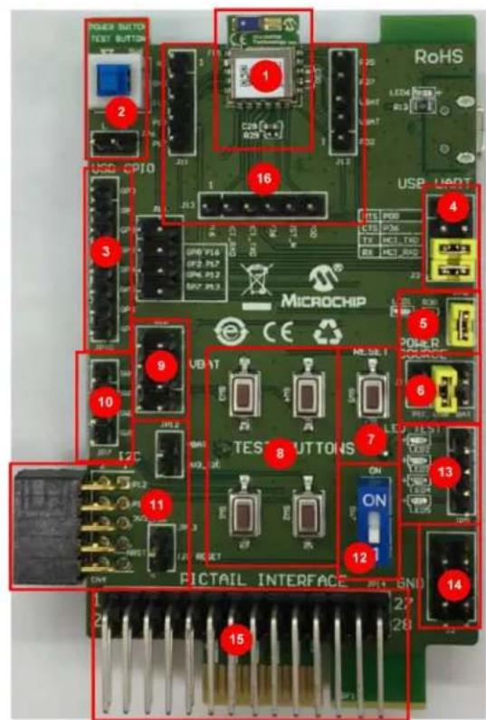
Figure 3-4 illustrates the top view of the BM70 EVB and Table 3-4 provides the details of the components.
TABLE 3-4: BM71 EVB COMPONENTS (BOTTOM VIEW)
| Block reference Component reference Description | |
| 1 — USB to UART converter (MCP2200) | |
| 2 SK1 Coin Cell battery holder (CR2032) |
FIGURE 3-4: BM71 EVB (BOTTOM VIEW)

3.3 HARDWARE FEATURES
This section describes the hardware features of the BM70/71 EVB. The BM70/71 EVB provides many options for communicating with other peripheral devices and connecting to various power sources, as illustrated in Figure 3-5 and Figure 3-6.
FIGURE 3-5: BM70 EVB BLOCK DIAGRAM

flowchart
graph TD
    A["Test Buttons (SW1 to SW4)"] --> B["Module Test Interfaces (CN1 to CN3)"]
    C["Power Switch Test Button (SW6)"] --> B
    D["LED Test (LED2 to LED5, JP5)"] --> B
    E["USB-to-UART Converter (P1, U10, J3, JP10, SW8)"] --> F["Power Source Option (J1)"]
    G["Coin Cell Battery CR2032 Socket (SK1)"] --> H["Power Source Option (J1)"]
    I["PICtail™ Interface (J8)"] --> H
    F --> J["BM70BLES1FC2 Module (FP2)"]
    H --> J
    J --> K["LED1 (blue)"]
    J --> L["Serial Flash Interface (J4)"]
    J --> M["I²C Interface (CN4, JP12, JP13)"]
    K --> N["Reset Button (SW5)"]
    L --> N
    M --> N
    style A fill:#f9f,stroke:#333
    style C fill:#f9f,stroke:#333
    style D fill:#f9f,stroke:#333
    style E fill:#ccf,stroke:#333
    style F fill:#cfc,stroke:#333
    style G fill:#fcc,stroke:#333
    style H fill:#fcc,stroke:#333
    style I fill:#fcc,stroke:#333
    style J fill:#cff,stroke:#333
    style K fill:#ffc,stroke:#333
    style L fill:#ffc,stroke:#333
    style M fill:#ffc,stroke:#333
    subgraph Power Source Options
        F -->|USB_5V| H
        F -->|USB_3V3| H
        F -->|BAT| H
        F -->|PIC_3V3| H
        G -->|USB_5V| H
        G -->|LED6 (red)| H
        H -->|VBAT| J
    end
    subgraph Module Interfaces
        B -->|VBAT| J
        B -->|VBAT| J
        B -->|VBAT| J
        B -->|VBAT| J
        B -->|VBAT| J
        B -->|VBAT| J
        B -->|VBAT| J
        B -->|VBAT| J
        B -->|VBAT| J
        B -->|VBAT| J
        B -->|VBAT| J
    end
FIGURE 3-6: BM71 EVB BLOCK DIAGRAM

flowchart
graph TD
    A["Power Switch Test Button (SW6, JP6)"] --> B["LED Test (LED2 to LED5, JP5)"]
    C["Test Buttons (SW1 to SW4)"] --> D["Module Test Interfaces (CN1 to CN3)"]
    E["USB-to-UART Converter (P1, U2, U10, J3, JP10, J14 SW8)"] --> F["Power Source Option (J1)"]
    G["Coin Cell Battery CR2032 Socket (SK1)"] --> H["Power Source Option (J1)"]
    I["PICtail™ Interface (JP14, GF1)"] --> H
    F --> H
    H --> J["BM71BLES1FC2 Module (FP1)"]
    K["LED6 (red)"] --> F
    L["USB_3V3"] --> H
    M["PIC_3V3"] --> H
    N["VBAT"] --> H
    O["VBAT"] --> P["LED1 (blue)"]
    Q["VBAT"] --> P
    R["I²C Interface (CN4, JP12, JP13)"] --> P
    S["Configuration DIP Switch (JP7)"] --> P
    T["Reset Button (SW5)"] --> P
    U["External Wire Connection"] -.-> V["Power Trace"]
    W["External Wire Connection"] -.-> X["Power Trace"]
The following list provide the details of each component in the BM70/71 EVB. For the location of these components, refer to Figure 3-1 through Figure 3-4.
3.3.1 Power Supply
There are three options to supply power to the module and board:
- Coin cell battery (Socket SK1 for CR2032 battery)
- USB
- PICtail™ socket connection (popular form factor to connect peripherals to other Microchip microcontroller development/starter kits)
The use of each option requires the appropriate change to the jumper on the J1 header of the EVB. This header also provides a convenient test/probe point to perform a current measurement to verify the BM70/71 module current draw (make sure LED1 is not connected to module, see 3.3.4 "LEDs"). One side of the header row provides a test point for the input power source, and the other side connects to the VBAT signal of the module (refer to Appendix A. "BM70 EVB Schematics" and Appendix B. "BM71 EVB Schematics").
3.3.2 USB to UART Connection
The BM70/71 EVB provides a UART interface to communicate with a host. The BM70/71 module makes the appropriate connections and provides a USB to UART converter IC on the EVB. This allows the BM70/71 module on the EVB to get power from and communicate with a PC. This makes it easy to use the Microchip provided tools for quick evaluation of the module when a host microcontroller is not available (see Firmware_SoftwareTools_Vx_xx.zip on Microchip product page). These tools use the same protocols referred to in Chapter 2. "Operating Modes, Configuration and Control".
BM70/71 Bluetooth® Low Energy Module User's Guide BM70/71 PICtail™/PICtail Plus EVB
3.3.2.1 CONNECTING AN EXTERNAL BM70/71 MODULE
Because the EVB routes the communication and control signals to various headers, a user can easily make blue wire connections for various test activities. One of these activities is leveraging the MCP2200 USB to UART converter IC to communicate with a module external to the EVB for testing purposes. This allows a user to communicate with and test a BM70/71 module through PC-based tools. Figure 3-7 illustrates how a user can make the blue wire connections to route the communication lines to the external BM70/71 module, bypassing the on-board module of the EVB.
FIGURE 3-7: UART CONNECTION TO BM70 EVB DUT

3.3.3 Push Buttons and Switches
There is no specific intended purpose for the push buttons or switches on the BM70/71 EVB apart from the Reset push button and mode DIP switch. The user has to determine how these hardware features may be used in the evaluation of the BM70/71 module. However, this use is not mandated.
The following list provides the description of the push buttons or switches and the features used to evaluate the BM70/71 EVB.
- SW1 through SW4 – Push button switches, with one side connected to ground/common, and the other side connected to the JP5 header. When the switch is pressed, it makes an electrical connection between ground and the header pin. The signal attached to the header can be the user's choice. The user can evaluate some features of the BM70/71 module with these switches, listed as follows:
- By making the necessary blue wire connection between pins on the JP5 header and the applicable digital I/O pin (refer to 1.1.2.2.1 “Manual Operation – General I/O”) on the module (accessed by the CN1 through CN3 connectors/pads), a user can test the built-in digital GPIO read control of the module
- SW5/Reset – This push button is used to drive the RST_N signal of the module to low. This resets the BM70/71 module and causes the mode pin (P2_0) level to be latched again (for the description of the pin, refer to 2.1 “Hardware Interface” and 2.2 “BM70/71 Mode Selection”).
- SW6 – This is a single throw, dual/two pole latching push button switch (DPST or 2PST). One contact (pole) is connected through a pull up resistor to Vcc/VBAT (the source can be USB, PICtail, or Coin Cell battery). The other contact is connected to ground/common on the EVB. When the switch is pressed, the two contacts are electrically connected to a 2-pin header, JP6. The user can evaluate some features of the BM70/71 module with this switch listed as follows:
- By making the necessary blue wire connection between pins on the JP6 header and the applicable digital I/O pin (refer to 1.1.2.2.1 “Manual Operation – General I/O”) on the module (accessed by the CN1 through CN3 connectors/pads), a user can test the built-in digital GPIO read control of the module
- SW7/DIP switch – This switch is connected to pin P2_0 on the BM70/71 module and is used to drive the pin to a logic level of "0". When the switch is in the "ON" or "1" position, pin P2_0 is electrically connected through a pull down resistor to ground/common. When the switch is in the "OFF" position, the connection is open. Pin P2_0 is pulled up internally on the module so when the switch is in "OFF" position, a user must see a logic level of "1" on pin P2_0 (for the description of the pin, refer to 2.1 "Hardware Interface" and 2.2 "BM70/71 Mode Selection")
- SW8 – This is a push button switch used to reset the MCP2200 USB to UART converter IC. If a user is seeing errant communication between the PC and the BM70/71 EVB, this push button can be used to reset the internal logic of the USB to UART converter IC.
3.3.4 LEDs
There are six LEDs on the BM70/71 EVB. These LEDs are used to give the user a visual indication of the BM70/71 module activity/status (for more details, refer to 1.1.2.3.1 "General Operation – LED Indication"). However, only one LED (LED1) has a specific intended purpose. The other four LEDs (LED2 to LED5) can be used for any other purpose determined by the user.
The following describes the LED hardware features on the BM70/71 EVB:
- LED1 – This LED is electrically connected to pin 2 on the JP8 header and pin P0_2 of the BM70/71 module. Pin 1 of the JP8 header is connected to VBAT/VCC. When a jumper is placed on pin 1 and pin 2 of the JP8 header, the LED will function based on the pattern being driven on pin P0_2 of the BM70/71 module. The BM70/71 module can drive a sequence of patterns (related to internal behavior occurring in the module) on pin P0_2 to cause LED1 to toggle on/off. This gives the user a visual indication when certain Bluetooth or module activity is occurring (for more details, refer to 1.1.2.3.1 “General Operation – LED Indication”). When verifying the current draw of the module, the jumper on the JP8 header needs to be removed if pin P0_2 has been configured to drive LED1. With the jumper in place, the current meter will read the current draw of the module and LED1. This will cause a mismatch between the values stated in the data sheet and the current meter measurement.
- By default, the LED connected to the P0_2 pin is driven to indicate the following states for the corresponding blinking pattern sequence:
- One blink: Standby mode
- Double blink: Link state
- LED2 through LED5 – These LEDs are connected to the JP5 header and a pull up resistor to VBAT/Vcc. The user can apply a logic level "0" to the applicable pin on JP5 to turn on the respective LED. The user determines what these LEDs must represent. The user can evaluate some features of the BM70/71 module with these LEDs as follows:
- By making the necessary blue wire connection between pins on the JP5 header and the applicable digital I/O pin (refer to 1.1.2.2.1 "Manual Operation – General I/O") on the module (accessed by the CN1 through CN3 connectors/pads), a user can test the built-in digital GPIO write control of the module.
- LED6 – This LED is connected to the USB V bus signal. When power is applied through the micro-USB connector, the LED will turn ON. This LED turns On only when power is supplied by the USB.
3.3.5 Jumpers
Table 3-5 through Table 3-11 provide details of the headers/jumpers hardware functionality on the BM70/71 EVB.
Table 3-5 provides the details of header J3 to connect the UART signals from the MCP2200 to the BM70/71 module.
TABLE 3-5: USB TO UART INTERFACE U10 (HEADER J3)
| Component Reference | Header Pin | EVB Signal Name | Description |
| J3 1 RTS MC | P2200 RTS pin | ||
| 2 P0_0 | BM70/71 GPIO | P0_0 (pin 15 on BM70 EVB and pin 11 on BM71 EVB)Can be configured as CTS for UART function when connected Jumper to pin1 of the header J3 | |
| 3 CTS | MCP2200 CTS | pin | |
| 4 P3_6 | BM70/71 GPIO | P3_6 (pin17 on BM70 EVB and pin 9 on BM71 EVB)Can be configured as RTS for UART function when connected Jumper to pin 3 of the header J3 | |
| 5 TX | MCP2200 RX pin | ||
| 6 HCI_TXD | BM70/71 UART Transmit (pin 23 on BM70 EVB and pin 8 on BM71 EVB)Connected Jumper to pin 5 of the header J3 | ||
| 7 Rx | MCP2200 | Tx pin | |
| 8 | HCI_RXD | BM70/71 HCI_RXD (pin 22 of BM70 EVB and pin 7 of BM71 EVB)Connected jumper to pin 7 of the header J3 | |
Table 3-6 provides the details of the headers, J10 and J2, which are available for accessing the VBAT and ground/common signal of the BM70/71 EVB.
TABLE 3-6: VBAT AND GROUND CONNECTOR (J10 AND J2)
| Component Reference | Header Pin | EVB Signal Name | Description |
| J10 | 1 to 8 | VBAT | Test points for probing VBAT signal on the BM70/71 EVB |
| J2 | 1 to 8 | GND | Test points for probing GND signal on the BM70/71 EVB |
Header JP10 is used for accessing the GPIO functionality of the MCP2200 (USB to UART Converter) IC. The signals connected to the GPIO pins of the MCP2200 can be read and driven. On the BM70/71 EVB, they are used to serve as the input for the BM70/71 module output status signals (for a description of signals in Auto Operation, refer to 1.1.2.1.2 "Auto Operation – Status Indication" and 1.1.2.1.5 "Auto Operation – Pairing Key" through 1.1.2.1.8 "Auto Operation – Link Quality Indication"), allowing the Auto Operation Tool to detect the state of the BM70/71 module. A blue wire connection must be made between the header and BM70/71 module pins.
Table 3-6 provides the details of header JP10, used for accessing the GPIO functionality of the USB to UART on the BM70/71 EVB.
TABLE 3-7: GPIO FUNCTIONALITY OF USB TO UART (HEADER JP10)
| Component Reference | Header Pin | EVB Signal Name | Description |
| JP10(BM70/71 EVB) | 1 GPO0 | Connect to the | the UART_RX_IND pin of the BM70/71 module. This functionality can be used in both Manual and Auto Operation(Pin is configurable, for more details, refer to 1.1.2.3.5 “General Operation – UART Receive Indication”) |
| 2 GPO1 | Connect to the | the LINK_DROP pin of the BM70/71 module. This functionality works only in Auto Operation(Pin is configurable, for more details, refer to 1.1.2.1.6 “Auto Operation – Link Drop”) | |
| 3 GPO2 | Connect to the | the PARING_KEY pin of the BM70/71 module. This functionality works only in Auto Operation(Pin is configurable, for more details, refer to 1.1.2.1.5 “Auto Operation – Pairing Key”) | |
| 4 GPO3 | Connect to the | the LOW_BATTERY_IND pin, or RSSI_IND pin of the BM70/71 module. This functionality works only in Auto Operation(Pin is configurable, for more details, refer to 1.1.2.1.7 “Auto Operation – Low Battery Indication” and 1.1.2.1.8 “Auto Operation – Link Quality Indication”) | |
| 5 | G | ||
| 6 | G | ||
| 7 GPO6 | Connect to the | the STATUS1_IND pin of the BM70/71 module. This functionality works only in Auto Operation(Pin is configurable, for more details, refer to 1.1.2.1.2 “Auto Operation – Status Indication”) | |
| 8 GPO7 | Connect to the | the STATUS2_IND pin of the BM70/71 module. This functionality works only in Auto Operation(Pin is configurable, for more details, refer to 1.1.2.1.2 “Auto Operation – Status Indication”) |
Table 3-8 provides details of header JP12, used to power an external I 2 C based peripheral on the BM70/71 EVB.
TABLE 3-8: I2C INTERFACE (HEADER JP12)
| Component Reference | Header Pin | EVB Signal Name | Description |
| JP12 1 VBAT | Sort with a jumper to power I2C peripheral from VBM70/71 EVB VBAT signal I | ||
| 2 | 3 2C |
Note: The jumper JP12 must be connected as default.
Table 3-9 provides details of header JP13, which is used to reset an external I 2 C based peripheral. The I 2 C peripheral will have a hardware pin reset function and will reset with a low true signal.
TABLE 3-9: CONNECTOR JP13
| Component Reference | Header Pin | EVB Signal Name | Description |
| JP13 1 RST_N | Short with a jumper to have RST_N connected to the I2C peripheral reset signal, attached to pin 2 of this header | ||
| 2 | 2C peripherals Reset Signal | This is the I2C peripheral's reset signal. The peripheral's reset signal must be low true. |
Table 3-10 provides details of headers J1, JP5, JP6, JP7, and JP8, which are the test points for the push buttons/switches, module power supply input selection, and LEDs of the BM70/71 EVB.
TABLE 3-10: POWER SOURCE OPTION CONNECTOR
| Component Reference | Header Pin | EVB Signal Name | Description |
| J1, JP5, JP6, JP7, and JP8 | — — These headers and module functionality are covered in the sections above (refer to 3.3.1 “Power Supply” through 3.3.4 “LEDs”) | ||
BM70/71 Bluetooth® Low Energy Module User's Guide BM70/71 PICtail™/PICtail Plus EVB
Table 3-11 provides details of header J4, which is used to provide access to the BM70 SPI peripheral. The SPI peripheral is only available for SDK users.
TABLE 3-11: SERIAL FLASH INTERFACE J4 (BM70 ONLY)
| Component Reference | Header Pin | EVB Signal Name | Description |
| J4 1 V | BAT BM70 EVB power signal | ||
| 2 | P | 3 _ 1 S | |
| 3 | P | 3 _ 2 S | |
| 4 | P | 3 _ 3 S | |
| 5 | P | 3 _ 4 S | |
| 6 | GND | Ground/common signal of BM70 EVB | |
| Note: The SPI peripheral is not available with firmware version 1.03 or 1.06 as listed on Microchip's BM70/71 module product pages. This header is only listed here for completeness. Contact your local Microchip representative for further details on the BM70 SPI peripheral. | |||
3.3.6 Connecting an External Host MCU
The EVB routes module communication and control signals to various headers. A user can easily make blue-wire connections for various test activities. To help with the early stages of prototyping, it may be advantageous to connect an external MCU to the BM70/71 module on the EVB for testing purposes. Figure 3-8 illustrates the connection in which the code can be developed and tested for the external MCU before target hardware has been fully developed.
FIGURE 3-8: UART CONNECTION TO HOST MICROCONTROLLER DUT
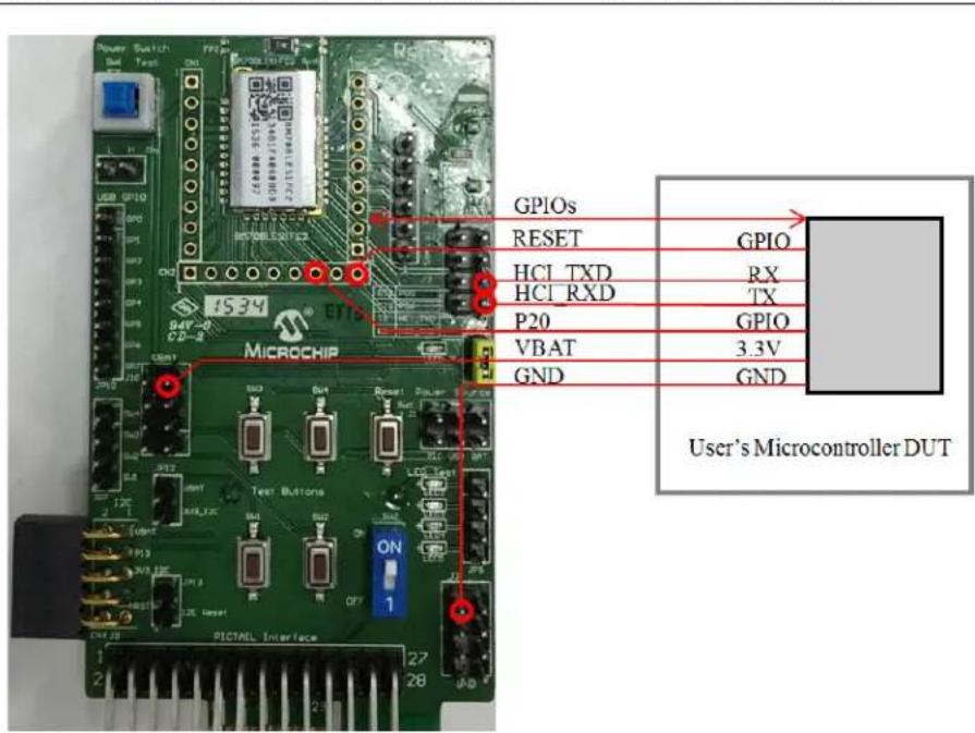
3.4 GETTING STARTED - BM70/71 EVB EXAMPLE CONFIGURATION
This section provides an understanding of the work flow for evaluating the BM70/71 module. The steps in the sub-sections show a procedure for updating the configuration parameters of the BM70/71 module using the EVB. The procedure demonstrates the connection between the BM70/71 module and smartphone that can be made. The data is exchanged between the BM70/71 module and smartphone app, using the proprietary "Transparent UART" service.
3.4.1 Requirements
The following hardware and software are required for getting started with the BM70/71 EVB.
3.4.1.1 HARDWARE REQUIREMENTS
• BM70/71 EVB
- Bluetooth-enabled smartphone
- i P h 8 46 er later version (it must support Bluetooth Low Energy) or
- Android™ device running Android 4.3 or later version
- Windows ® host PC with USB port
- Micro-USB cable
3.4.1.2 SOFTWARE REQUIREMENTS
Download and install the latest firmware and corresponding tools (Firmware_SoftwareTools_Vx_xx.zip) from the Microchip website: www.microchip.com/BM70 for BM70 EVB and www.microchip.com/BM71 for BM71 EVB.
- Firmware update tool (BM7xBLE_IS187x_FlashUpdateTool.exe)
- Firmware hex images (*.H00, *.H01, *.H02, *H03)
- Configuration tool (IS187x_102_BLEDK3_UI_v100.xxx.exe)
- mBIoT Utility app, available at App Store® for iPhone and at Google Play™ for Android
Note 1: Ensure the latest firmware is downloaded to the IS1870/71 IC on the BM70/71 EVB. The initial Bluetooth Low Energy firmware version programmed into BM70 modules in Microchip's manufacturing line at the time of releasing this product to market was version 1.03. The initial Bluetooth Low Energy firmware version programmed into BM71 modules in Microchip's manufacturing line at the time of releasing this product to market was version 1.06. The latest firmware for each module is made available on the BM70 and BM71 product web pages on Microchip's website. For more details, refer to 3.5.1 "Programming Procedure".
2: Ensure the exact version of the Configuration tool (UI Tool) matches the specific firmware version programmed into the IS1870/71 IC's Flash memory is used to configure the module. For ease of use, the UI tool, firmware and firmware update utility are all provided in a single zip file for each version of firmware released by Microchip to the website. The latest firmware for the BM70/71 module is not compatible with older versions of the Configuration tool. To ensure the correct version of firmware and tools are being used together, a Firmware_Software_Vx_xx.zip file is provided. This archive contains firmware along with the compatible software tools for this specific firmware version.
3: In the following example, the BM70 EVB with firmware version 1.03 and Configuration tool (IS187x_102_BLEDK3_UI v100.123.exe) is used.
3.4.2 Setting Configuration Parameters
The Configuration tool or User Interface (UI) tool is a PC based program, which enables the user to change the configuration parameters of the BM70/71 EVB (for hardware details on configuration, refer to 2.1 "Hardware Interface"). The following list provides some examples of the parameter settings that can be updated on the BM70 module using the UI tool (for the description of features, refer to 1.1.1 "Configuration Overview"):
- Device name
- UART settings
- Bluetooth Low Energy connection settings
- Add or edit GATT service table.
Perform the following actions to update the UI parameter settings:
- Open the UI tool and click Load, see Figure 3-9. The Loading Option window is displayed.
Note 1: Download and unzip the contents of the Firmware_Software-Tools_Vx_xx.zip file, which is available at the Microchip website: www.microchip.com/BM70 or www.microchip.com/BM71. The configuration tool is part of this zip file content and located under the sub-folder "ConfigurationTool". In this demonstration, the IS187x_102_BLED-K3_UI_Configuration_Tool v100.123.exe tool is used. This tool version corresponds to firmware version v1.03. This information is shown in by the file name, Firmware_SoftwareTools_Vx_xx.zip, where "Vx_xx" is the firmware version.
2: For the BM71 EVB, the IS187x_102_BLEDK3v1.06_UI1.02 tool version must be used, which is available on the Microchip website: www.microchip.com/BM71. This version corresponds to firmware version 1.06.
FIGURE 3-9: CONFIGURATION TOOL WINDOW

- In the Loading Option window, click Load Text File to load default configuration parameters, see Figure 3-10.
FIGURE 3-10: LOADING OPTION WINDOW

- From the Open dialog, select the default configuration parameter text file (provided with the Firmware_SoftwareTools_Vx_xx.zip file under the "ConfigurationTool/" sub-folder) and then click Open, see Figure 3-11.
FIGURE 3-11: OPEN DIALOG BOX

- From the Configuration Tool window, click Edit to start editing the default parameters, see Figure 3-12.
FIGURE 3-12: CONFIGURATION TOOL WINDOW

- From the Main Feature window, click BLEDK and then click OK, see Figure 3-13.
FIGURE 3-13: MAIN FEATURE WINDOW

- The UI tool displays a window with various configuration options (tabs) in tabular format. Click the System Setup tab, and in the Name fragment box, type "BM70_BLE" (or any user-defined name), see Figure 3-14.
Note 1: Click the Help button to get information related to UI parameters. 2: The Auto Operation setting is chosen by default. For more details on BM70/71 behavior under Auto Operation, refer to 1.1.2.1 "Auto Operation".
FIGURE 3-14: CONFIGURING PARAMETERS - SYSTEM SETUP
![System Setup System Setup2 LE Mode Setup GATT Service Table LED Setup Beacon Setup Device Information Name Fragment BM70_BLE [32 characters] Uart Setting HCI Baud Rate Index 0x03 : 115200 Help H/W Flow Control Disable Check Rx Data Interval 0x 00 (unit: 0.625ms) total : 0.000 ms UART RX_IND Enable Operation Mode Setting Operation Pattern Auto Pattern Help Configure Mode Timeout 0x 00 (0:Disable Configure Mode, unit: 640ms) total : 0 ms Standby Mode Setting Power On Standby Time 0x 0C Help Previous Next Finish](/content/2026/06/1360921/images/a0dc0da6bb778790d1b5dc25322514e784dad68d0bcdf0b75d603aedfd6f4296.jpg)
- Click the LE Mode Setup tab and under the Advertising Data Setting section, select Device Name to advertise the device name, see Figure 3-15. This ensures that the name fragment is included in the advertising packet.
FIGURE 3-15: ADVERTISING DATA SETTING

- Click Finish. The Configuration Tool main window is displayed, see Figure 3-16.
FIGURE 3-16: CONFIGURATION TOOL MAIN WINDOW

-
From the Configuration Tool window, perform any one of these actions:
-
Click Save to save the selected parameter settings as .txt or .hex files (for later production programming).
- Click Export to export a log file along with the parameters to a .txt file. The log file contains the settings of configuration parameters, which were edited.
-
Click Write to program these configuration settings into the BM70/71 module. For this to function, the BM70/71 module must be in Configuration mode.
-
To program the configuration parameters on the BM70 module, perform these actions:
a) Set switch SW7 in the "ON" or "1" position (configuration mode), see Figure 3-17.
FIGURE 3-17: SW7 IN TEST MODE

b) Ensure that jumpers J1, JP8 and J3 on the BM70 EVB are connected, as illustrated in Figure 3-18.
FIGURE 3-18: JUMPER AND BM70 EVB CONNECTION DETAILS

c) Connect the USB port (P1) of the BM70 EVB to a PC using the micro-USB cable, see Figure 3-19.
FIGURE 3-19: CONFIGURATION SETUP

d) On connection, LED1 (blue) and LED6 (red) on the BM70 EVB will turn ON.
e) Go to the Configuration Tool window and click Write to program the settings into the internal memory of the BM70/71 module, see Figure 3-16.
f) The Read/Write Flash window is displayed. Select the values for COM Port and Baudrate (must be 115200 for the configuration to succeed), and then click Write, see Figure 3-20.
FIGURE 3-20: READ/WRITE FLASH

g) A message box will appear displaying the message "Write Flash Finish". Click OK to finish, see Figure 3-21.
3.4.3 Bluetooth Low Energy Connection to a Smartphone
This section lists the steps to put the BM70/71 into "Application/Run" mode after setting up the configuration parameters. Perform the following actions to establish a Bluetooth Low Energy connection between the BM70/71 EVB and a smartphone. An iPhone with iOS9.2.1 is used for this demonstration.
- Download the mBIoT app from the App Store and enable the Bluetooth settings on the iPhone (In this example illustration an iPhone was used, but a user can do the same operation on an Android based smartphone).
- Set switch SW7 to the OFF position (the P2_0 pin will be pulled high through an internal pull up of IS1870/71 chip) on the BM70 EVB, see Figure 3-22.
FIGURE 3-22: SW7 IN APPLICATION MODE
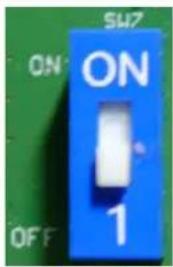
- Connect the BM70 EVB to a PC using the micro-USB cable, see Figure 3-23. LED6 (red) will turn ON solid when USB power is applied to the EVB. LED1 (blue) will turn ON for 50 ms once every three seconds to visually indicate the device is sending connectable advertising packets (standby mode).
Note: Based on the default configuration parameters, the BM70/71 module is setup to advertise for a max of 122 seconds (for more details, refer to 1.1.2.1.10 "Auto Operation – Discoverability"). If LED1 stops flashing/toggling, the device has entered into the Deep-sleep state and has stopped sending advertising packets. Pushing the reset button will restart the BM70/71 module and device will start to advertise again.
FIGURE 3-23: POWER-ON BM70 EVB

- Enable the Bluetooth settings of the phone and then open the mBIoT app, see Figure 3-24.
FIGURE 3-24: ENABLING BLUETOOTH AND MBIOT APPLICATION

- After the mBIoT app is opened, a user is presented with several choices for communicating with different Microchip Bluetooth modules. Select BM70/BM71 Bluetooth Low Energy UART, see Figure 3-25.
FIGURE 3-25: SELECT BM70/BM71 BLUETOOTH LOW ENERGY UART

- A list of discoverable devices will be displayed; select the device with the name BM70_BLE to connect with BM70 module, see Figure 3-26.
FIGURE 3-26: DISCOVERED DEVICES VIEW

- Under Connected Device, tap BM70_BLE connected for the device information feature, see Figure 3-27
FIGURE 3-27: CONNECTED DEVICE VIEW

- Select Device Info to check the device information, see Figure 3-28.
FIGURE 3-28: DEVICE INFORMATION
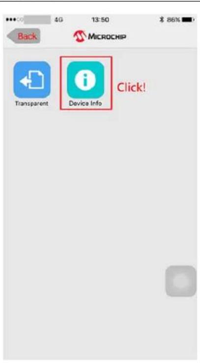
BM70/71 Bluetooth® Low Energy Module User's Guide BM70/71 PICtail™/PICtail Plus EVB
- The device information will be displayed, showing the Bluetooth Low Energy connection has been made between the phone app and the BM70 module, see Figure 3-29.
FIGURE 3-29: DEVICE INFORMATION
![Back MICROCHIP Manufacture Name: ISSC Model Number: BM70 Serial Number: 0000 Hardware Revision: 5505 102_BLDK3 Firmware Revision: 010300 Software Revision: 0000 System ID: <00000000 00000000> Specific UUID1: Specific UUID2: [Regulatory Certification Data List] 000000000100000 Count: 0x0000 Lon: 0x0000 Device Information!](/content/2026/06/1360921/images/a833a083bbde2c6741308e6b082cebec87e49f6a15b658a0984d3b8873c8006a.jpg)
- The Bluetooth Low Energy link connection is established between the BM70 EVB and an iPhone, see Figure 3-30.
FIGURE 3-30: BLUETOOTH LOW ENERGY LINK CONNECTION

3.5 FIRMWARE PROGRAMMING PROCEDURE
Programming the firmware is required to update to a newer version, or to load a specific version into the device. This section describes the process of programming firmware into the IS1870/71 IC on the BM70/71 module. Microchip provides a PC based tool, referred to as the "ISUpdate_Tool.exe", for performing the firmware programming operation. This tool inputs the firmware hex image files (see 3.4.1.2 "Software Requirements" for getting firmware hex images) for the BM70/71 and uses the Programming Protocol (see 2.5 "Programming Protocol") to program them into the device.
3.5.1 Programming Procedure
The procedure shows an example of the work flow for programming firmware into the device. This demonstration programs version 1.03 of the firmware into the BM70 module on the EVB. This demonstrated work flow can be repeated for any firmware version compatible with the BM70/71 module. To program firmware, perform the following actions:
- Download the Firmware_SoftwareTools_Vx.xx.zip file from the Microchip website: www.microchip.com/BM70 for the BM70 EVB and www.microchip.com/BM71 for the BM71 EVB. Unzip the file and locate the firmware update tool called ISUpdate_Tool.exe under the "Firmware_Firmware-Tools/" sub-folder. Locate the firmware hex image files with the file extension "*.H00, *.H01, *.H02, and *.H03" under the sub-folder "Firmware_FirmwareTools/Firmware/". In the following example, firmware version 1.03 will be programmed into the BM70 module. The firmware update tool and firmware hex images will be required for this example.
- Set switch SW7 in the ON position (refer to 2.2 "BM70/71 Mode Selection"), see Figure 3-31.
FIGURE 3-31: SW7 IN TEST MODE
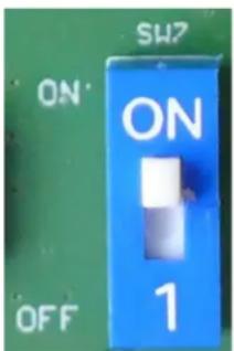
- Ensure that jumpers, J1, JP8 and J3 on the BM70 EVB are connected, as illustrated in Figure 3-18.
- Connect the BM70 EVB to a PC using a micro-USB cable, see Figure 3-32. On connection, LED6 (red) and LED1 (blue) will turn on. Press the Reset button (SW5) to reset the BM70 module.
FIGURE 3-32: FIRMWARE PROGRAMMING SETUP

-
Open the firmware update tool isupdate.exe. Select the COM port and set the following parameters in the tool (see Figure 3-33):
-
Baud Rate: 115200
- Memory type/subtype: Flash/Embedded Flash
-
Address: 0x0000
-
Click Connect. On successful connection, the log window will show the string "Port connect -> COM x" message will be displayed, see Figure 3-33.
FIGURE 3-33: FIRMWARE UPDATE TOOL WINDOW - PORT CONNECT

- If the connection was not successful, the log window will show the string "Connect failed". Verify the parameters input into the tool, press the reset push button on the EVB, and try to "Connect" again, see Figure 3-34.
FIGURE 3-34: FIRMWARE UPDATE TOOL WINDOW

BM70/71 Bluetooth® Low Energy Module User's Guide BM70/71 PICtail™/PICtail Plus EVB
- Click Browse to navigate to the folder where the firmware files (.hex) have been downloaded from the Microchip website. In the Open dialog, select all the four hex image files and then click Open, see Figure 3-35.
FIGURE 3-35: SELECTING THE FLASH CODE FILES

- In the Firmware Update tool window, click Update, see Figure 3-36.
FIGURE 3-36: FIRMWARE UPDATE

BM70/71 Bluetooth® Low Energy Module User's Guide BM70/71 PICtail™/PICtail Plus EVB
- The Firmware Update tool will start writing the selected firmware files into the device. Wait until the string "End of Write Memory!" with the elapse time is displayed in the log window, see Figure 3-37.
FIGURE 3-37: FIRMWARE UPDATE FINISH

-
To verify the firmware version, enter the following parameters under the Flash/EEPROM/MCU/AHB Access section, and then click Read, see Figure 3-38:
-
Address: 0x100E
- Length (Hex): 0x02
FIGURE 3-38: ENTERING PARAMETERS
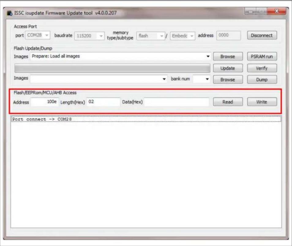
BM70/71 Bluetooth® Low Energy Module User's Guide BM70/71 PICtail™/PICtail Plus EVB
- The Data (Hex) box will display "01 03" and the log window will display the following string: "0x01 0x03". This number represents the firmware version the device has been programmed with, in this case version v1.03, see Figure 3-39.
FIGURE 3-39: VERIFY FIRMWARE VERSION

- After completing the firmware update, any configuration parameters will have been lost. The user should reprogram configuration parameters back into the device before switching to "Application/Run" mode.
Appendix A. BM70 EVB Schematics
A.1 BM70 EVB REFERENCE SCHEMATICS
FIGURE A-1: BM70 EVB SCHEMATICS

FIGURE A-2: BM70 EVB SCHEMATICS

Appendix B. BM71 EVB Schematics
B.1 BM71 EVB REFERENCE SCHEMATICS
FIGURE B-1: BM71 EVB SCHEMATICS
| BM71BLES1FC2 | Configuration OFF ON R3 SWI ON OFF MODE OFF APP Mode |
| Power Switch Test Button SWI PS-SUIT PushHigh 4K7.1% Connect to I/O for Switch Test | |
| Test Buttons Reset Button | |
| I²C Interface | LED for I/O Test VBAT R28 LED5 LED-SY LED-SY LED-SY LED-SY LED-SY LED-SY LED-SY LED-SY LED-SY LED-SY LED-SY LED-SY LED-SY LED-SY LED-SY LED-SY LED-SY LED-SY LED-SY LED-SY LED-SY LED-SY LED-SY LED-SY LED-SY LED-Sy LED-Sy LED-Sy LED-Sy LED-Sy LED-Sy LED-Sy LED-Sy LED-Sy LED-Sy LED-Sy LED-Sy LED-Sy LED-Sy LED-Sy LED-Sy LED-Sy LED-Sy LED-Sy LED-Sy LED-Sy LED-Sy LED-Sy LED-Sy LED-Sy LED-Ss LED-Ss LED-Ss LED-Ss LED-Ss LED-Ss LED-Ss LED-Ss LED-Ss LED-Ss LED-Ss LED-Ss LED-Ss LED-Ss LED-Ss LED-Ss LED-Ss LED-Ss LED-Ss LED-Ss LED-Ss LED-Ss LED-Ss LED-Ss LED-Ss LED-SS LED-SS LED-SS LED-SS LED-SS LED-SS LED-SS LED-SS LED-SS LED-SS LED-SS LED-SS LED-SS LED-SS LED-SS LED-SS LED-SS LED-SS LED-SS LED-SS LED-SS LED-SS LED-SS LED-SS LED-SS LED-Ss LED-s LED-s LED-s LED-s LED-s LED-s LED-s LED-s LED-s LED-s LED-s LED-s LED-s LED-s LED-s LED-s LED-s |
FIGURE B-2: BM71 EVB SCHEMATICS

Appendix C. Commands Summary Quick Reference
C.1 QUICK REFERENCE OF HOST TO BM70/71 MODULE COMMANDS
Table C-1 provides all commands the host can send to the BM70/71 module.
TABLE C-1: QUICK REFERENCE OF HOST TO BM70/71 MODULE COMMANDS
| Command Type Command Name | |
| Common Read Local Information (opcode - 0x01) | |
| GATT Client GATT Client - Discover All Primary Services (opcode - 0x30) | |
| GATT Server GATT Server - Send Characteristic Value (opcode - 0x38) | |
| GATT Server - Read Specific Local Primary Service (opcode - 0x3C) | |
C.2 QUICK REFERENCE OF BM70/71 MODULE TO HOST EVENT RESPONSES
Table C-2 provides all event responses the BM70/71 module can send to the host.
TABLE C-2: QUICK REFERENCE OF BM70/71 MODULE TO HOST EVENT RESPONSES
| Event Type Event Name | |
| Pairing / Bonding Pairing | - Passkey Entry Request Event (opcode - 0x60) |
| Pairing - Pair Complete Event (opcode - 0x61) | |
| Pairing - Passkey Confirm Request Event (opcode - 0x62) | |
| GAP Advertising | Report Event (opcode - 0x70) |
| LE Connection Complete Event (opcode - 0x71) | |
| Disconnect Complete Event (opcode - 0x72) | |
| Connection Parameter Update Event (opcode - 0x73) | |
| Common Command | Complete Event (opcode - 0x80) |
| Status Report Event (opcode - 0x81) | |
| Configure Mode Status Event (opcode - 0x8F) | |
| GATT Discover | all Primary Services Event (opcode - 0x90) |
| Discover Specific Primary Service Characteristic Declaration Event (opcode - 0x91) | |
| Discover All Characteristic Descriptors Event (opcode - 0x92) | |
| GATT Server - Client Write Characteristic Value Event (opcode - 0x98) | |
| GATT Transparent - Received Transparent Data Event Response (opcode - 0x9A) | |
Worldwide Sales and Service
AMERICAS
Corporate Office
2355 West Chandler Blvd.
Chandler, AZ 85224-6199
Tel: 480-792-7200
Fax: 480-792-7277
Technical Support:
http://www.microchip.com/
support
Web Address:
www.microchip.com
Atlanta
Duluth, GA
Tel: 678-957-9614
Fax: 678-957-1455
Austin, TX
Tel: 512-257-3370
Boston
Westborough, MA
Tel: 774-760-0087
Fax: 774-760-0088
Chicago
Itasca, IL
Tel: 630-285-0071
Fax: 630-285-0075
Dallas
Addison, TX
Tel: 972-818-7423
Fax: 972-818-2924
Detroit
Novi, MI
Tel: 248-848-4000
Houston, TX
Tel: 281-894-5983
Indianapolis
Noblesville, IN
Tel: 317-773-8323
Fax: 317-773-5453
Tel: 317-536-2380
Los Angeles
Mission Viejo, CA
Tel: 949-462-9523
Fax: 949-462-9608
Tel: 951-273-7800
Raleigh, NC
Tel: 919-844-7510
New York, NY
Tel: 631-435-6000
San Jose, CA
Tel: 408-735-9110
Tel: 408-436-4270
Canada - Toronto
Tel: 905-695-1980
Fax: 905-695-2078
ASIA/PACIFIC
Australia - Sydney
Tel: 61-2-9868-6733
China - Beijing
Tel: 86-10-8569-7000
China - Chengdu
Tel: 86-28-8665-5511
China - Chongqing
Tel: 86-23-8980-9588
China - Dongguan
Tel: 86-769-8702-9880
China - Guangzhou
Tel: 86-20-8755-8029
China - Hangzhou
Tel: 86-571-8792-8115
China - Hong Kong SAR
Tel: 852-2943-5100
China - Nanjing
Tel: 86-25-8473-2460
China - Qingdao
Tel: 86-532-8502-7355
China - Shanghai
Tel: 86-21-3326-8000
China - Shenyang
Tel: 86-24-2334-2829
China - Shenzhen
Tel: 86-755-8864-2200
China - Suzhou
Tel: 86-186-6233-1526
China - Wuhan
Tel: 86-27-5980-5300
China - Xian
Tel: 86-29-8833-7252
China - Xiamen
Tel: 86-592-2388138
China - Zhuhai
Tel: 86-756-3210040
ASIA/PACIFIC
India - Bangalore
Tel: 91-80-3090-4444
India - New Delhi
Tel: 91-11-4160-8631
India - Pune
Tel: 91-20-4121-0141
Japan - Osaka
Tel: 81-6-6152-7160
Japan - Tokyo
Tel: 81-3-6880-3770
Korea - Daegu
Tel: 82-53-744-4301
Korea - Seoul
Tel: 82-2-554-7200
Malaysia - Kuala Lumpur
Tel: 60-3-7651-7906
Malaysia - Penang
Tel: 60-4-227-8870
Philippines - Manila
Tel: 63-2-634-9065
Singapore
Tel: 65-6334-8870
Taiwan - Hsin Chu
Tel: 886-3-577-8366
Taiwan - Kaohsiung
Tel: 886-7-213-7830
Taiwan - Taipei
Tel: 886-2-2508-8600
Thailand - Bangkok
Tel: 66-2-694-1351
Tel: 43-7242-2244-39
Fax: 43-7242-2244-393
Denmark - Copenhagen
Tel: 45-4485-5910
Fax: 45-4485-2829
Finland - Espoo
Tel: 358-9-4520-820
France - Paris
Tel: 33-1-69-53-63-20
Fax: 33-1-69-30-90-79
Germany - Garching
Tel: 49-8931-9700
Germany - Haan
Tel: 49-2129-3766400
Germany - Heilbronn
Tel: 49-7131-72400
Germany - Karlsruhe
Tel: 49-721-625370
Germany - Munich
Tel: 49-89-627-144-0
Fax: 49-89-627-144-44
Germany - Rosenheim
Tel: 49-8031-354-560
Israel - Ra'anana
Tel: 972-9-744-7705
Italy - Milan
Tel: 39-0331-742611
Fax: 39-0331-466781
Italy - Padova
Tel: 39-049-7625286
Netherlands - Drunen
Tel: 31-416-690399
Fax: 31-416-690340
Norway - Trondheim
Tel: 47-7288-4388
Poland - Warsaw
Tel: 48-22-3325737
Romania - Bucharest
Tel: 40-21-407-87-50
Spain - Madrid
Tel: 34-91-708-08-90
Fax: 34-91-708-08-91
Sweden - Gothenberg
Tel: 46-31-704-60-40
Sweden - Stockholm
Tel: 46-8-5090-4654
UK - Wokingham
Tel: 44-118-921-5800
Fax: 44-118-921-5820


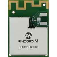
- Note the following details of the code protection feature on Microchip devices:
- Trademarks
- Table of Contents
- Chapter 1. Overview
- Chapter 2. Operating Modes, Configuration and Control
- Chapter 3. BM70/71 PICtail™/PICtail Plus EVB
- Preface
- NOTICE TO CUSTOMERS
- INTRODUCTION
- DOCUMENT LAYOUT
- CONVENTIONS USED IN THIS GUIDE
- RECOMMENDED READING
- BM70/71 Data Sheet (DS60001372)
- Bluetooth Core Specification
- THE MICROCHIP WEBSITE
- PRODUCT CHANGE NOTIFICATION SERVICE
- CUSTOMER SUPPORT
- DOCUMENT REVISION HISTORY
- Revision B (February 2021)
- Revision A (October 2016)
- Configuration Overview
- System Operation
- AUTO OPERATION
- Auto Operation – Transparent UART
- Auto Operation – Status Indication
- Auto Operation – Configuration Timeout
- Auto Operation – UART Flow Control
- Auto Operation – Pairing Key
- Auto Operation – Link Drop
- Auto Operation – Low Battery Indication
- Auto Operation – Link Quality Indication
- Auto Operation – BM70/71 Active Indication
- Auto Operation – Discoverability
- Auto Operation – Connections
- MANUAL OPERATION
- Manual Operation – General I/O
- Manual Operation – Analog Pins
- Manual Operation – Pulse Width Modulation (PWM) Output
- Manual Operation – GATT Services
- GENERAL OPERATION
- General Operation – LED Indication
- General Operation – Low Power Control
- General Operation – Wake-Up Indication
- General Operation - UART Transmit Indication
- General Operation – UART Receive Indication
- General Operation - Security
- HARDWARE INTERFACE
- BM70/71 MODE SELECTION
- COMMAND SET PROTOCOL
- General Message Format
- UART Interface Characteristics
- Commands and Event Responses
- READ LOCAL INFORMATION (OPCODE - 0X01)
- Command Format, Host to BM70/71 Module
- Defaults
- Example
- Response Format, BM70/71 to Host
- Applicable Configuration
- RESET (OPCODE - 0X02)
- Command Format, Host to BM70/71 Module
- Defaults
- Example
- READ BM70/71 STATUS (OPCODE - 0X03)
- Command Format, Host to BM70/71 Module
- Defaults
- Example
- Response Format, BM70/71 Module to Host
- Applicable Configuration
- READ BM70/71 ADC VALUE (OPCODE - 0X04)
- Command Format, Host to BM70/71 Module
- Defaults
- Example
- Response Format, BM70/71 Module to Host
- Applicable Configuration
- INTO SHUTDOWN MODE (OPCODE - 0X05)
- Command Format, Host to BM70/71 Module
- Defaults
- Example
- Response Format, BM70/71 Module to Host
- Applicable Configuration
- READ DEVICE NAME (OPCODE - 0X07)
- Command Format, Host to BM70/71 Module
- Defaults
- Example
- Response Format, BM70/71 Module to Host
- Applicable Configuration
- WRITE DEVICE NAME (OPCODE - 0X08)
- Command Format, Host to BM70/71 Module
- Defaults
- Example
- ERASE ALL PAIRED BONDED DEVICE INFORMATION (OPCODE - 0x09)
- Command Format, Host to BM70/71 Module
- Defaults
- Example
- Response Format, BM70/71 Module to Host
- Applicable Configuration
- READ PAIRING MODE SETTING (OPCODE - 0X0A)
- Command Format, Host to BM70/71 Module
- Defaults
- Example
- Response Format, BM70/71 Module to Host
- Applicable configuration
- WRITE PAIRING MODE SETTING (OPCODE - 0X0B)
- Command Format, Host to BM70/71 Module
- Defaults
- Example
- Response Format, BM70/71 Module to Host
- Applicable Configuration
- READ ALL PAIRED BONDED DEVICE INFORMATION (OPCODE - 0X0C)
- Command Format, Host to BM70/71 Module
- Defaults
- Example
- Response Format, BM70/71 Module to Host
- Applicable Configuration
- DELETE PAIRED BONDED DEVICE (OPCODE - 0X0D)
- Command Format, Host to BM70/71 Module
- Defaults
- Example
- Response Format, BM70/71 Module to Host
- Applicable Configuration
- DIGITAL INPUT/OUTPUT CONTROL (OPCODE - 0X0E)
- Command Format, Host to BM70/71 Module
- Defaults
- Example
- Response Format, BM70/71 Module to Host
- Applicable configuration
- PWM CONTROL (OPCODE - 0X0F)
- Command Format, Host to BM70/71 Module
- Defaults
- Example
- Response Format, BM70/71 Module to Host
- Applicable Configuration
- READ RSSI VALUE (OPCODE - 0X10)
- Command Format, Host to BM70/71 Module
- Defaults
- Example
- Response Format, BM70/71 Module to Host
- Applicable configuration
- WRITE ADVERTISING DATA (OPCODE - 0X11)
- Command Format, Host to BM70/71 Module
- Defaults
- Example
- Response Format, BM70/71 Module to Host
- Applicable Configuration
- WRITE SCAN RESPONSE DATA (OPCODE - 0X12)
- Command Format, Host to BM70/71 Module
- Defaults
- Example
- SET ADVERTISING PARAMETERS (OPCODE - 0X13)
- Command Format, Host to BM70/71 Module
- Default
- Example
- Response Format, BM70/71 Module to Host
- Applicable Configuration
- SET SCAN PARAMETERS (OPCODE - 0X15)
- Command Format, Host to BM70/71 Module
- Defaults
- Example
- Response Format, BM70/71 Module to Host
- Applicable Configuration
- SET SCAN ENABLE (OPCODE - 0X16)
- Command Format, Host to BM70/71 Module
- Defaults
- Example
- Response Format, BM70/71 Module to Host
- Applicable Configuration
- LE CREATE CONNECTION (OPCODE - 0X17)
- Command Format, Host to BM70/71 Module
- Default
- Example
- Response Format, BM70/71 Module to Host
- Applicable Configuration
- LE CREATE CONNECTION CANCEL (OPCODE - 0X18)
- Command Format, Host to BM70/71 Module
- Default
- Example
- Response Format, BM70/71 Module to Host
- Applicable Configuration
- CONNECTION PARAMETER UPDATE REQUEST
- Command Format, Host to BM70/71 Module
- Default
- Example
- Response Format, BM70/71 Module to Host
- Applicable Configuration
- DISCONNECT (OPCODE - 0X1B)
- Command Format, Host to BM70/71 Module
- Default
- Example
- Response Format, BM70/71 Module to Host
- SET ADVERTISING ENABLE\_DISABLE (OPCODE - 0X1C)
- Command Format, Host to BM70/71 Module
- Default
- Example
- Response Format, BM70/71 Module to Host
- Applicable Configuration
- READ REMOTE DEVICE NAME (OPCODE - 0X1F)
- Command Format, Host to BM70/71 Module
- Default
- Example
- Response Format, BM70/71 Module to Host
- Applicable Configuration
- GATT CLIENT - DISCOVER ALL PRIMARY SERVICES (OPCODE - 0X30)
- Command Format, Host to BM70/71 Module
- Default
- Example
- Response Format, BM70/71 Module to Host
- "Command Complete Event (opcode - 0x80)" and 2.3.3.54 "Discover All Primary Services Event (opcode - 0x90)".
- Applicable Configuration
- GATT CLIENT - DISCOVER SPECIFIC PRIMARY
- SERVICE CHARACTERISTIC (OPCODE - 0X31)
- Command Format, Host to BM70/71 Module
- Default
- Example
- Response Format, BM70/71 Module to Host
- Applicable Configuration
- READ CHARACTERISTIC VALUE (OPCODE - 0X32)
- Command Format, Host to BM70/71 Module
- Default
- Example
- Response Format, BM70/71 Module to Host
- Applicable Configuration
- GATT CLIENT - READ USING CHARACTERISTIC UUID (OPCODE - 0X33)
- Command Format, Host to BM70/71 Module
- Default
- Example
- Response Format, BM70/71 Module to Host
- "Command Complete Event (opcode - 0x80)".
- Applicable Configuration
- GATT CLIENT - WRITE CHARACTERISTIC VALUE
- (OPCODE - 0X34)
- Command Format, Host to BM70/71 Module
- Default
- Example
- Response Format, BM70/71 Module to Host
- Applicable Configuration
- GATT CLIENT - ENABLE TRANSPARENT UART SERVICE (OPCODE - 0X35)
- Command Format, Host to BM70/71 Module
- Default
- Example
- Response Format, BM70/71 Module to Host
- Applicable Configuration
- GATT SERVER - SEND CHARACTERISTIC VALUE
- Command Format, Host to BM70/71 Module
- Default
- Example
- Response Format, BM70/71 Module to Host
- Applicable Configuration
- GATT SERVER - UPDATE CHARACTERISTIC VALUE (OPCODE - 0X39)
- Command Format, Host to BM70/71 Module
- Default
- Example
- Response Format, BM70/71 Module to Host
- Applicable Configuration
- GATT SERVER - READ LOCAL CHARACTERISTIC VALUE (OPCODE - 0X3A)
- Command Format, Host to BM70/71 Module
- Default
- Example
- Response Format, BM70/71 Module to Host
- Applicable Configuration
- GATT SERVER - READ ALL LOCAL PRIMARY SERVICES (OPCODE - 0X3B)
- Command Format, Host to BM70/71 Module
- Default
- Example
- Response Format, BM70/71 Module to Host
- Applicable Configuration
- GATT SERVER - READ SPECIFIC LOCAL PRIMARY SERVICE (OPCODE - 0X3C)
- Command Format, Host to BM70/71 Module
- Default
- Example
- Response Format, BM70/71 Module to Host
- Applicable Configuration
- GATT SERVER - SEND WRITE RESPONSE (OPCODE - 0X3D)
- Command Format, Host to BM70/71 Module
- Default
- Example
- Response Format, BM70/71 Module to Host
- Applicable Configuration
- TRANSPARENT UART SERVICE - SEND DATA (OPCODE - 0X3F)
- Command Format, Host to BM70/71 Module
- Default
- Example
- Response Format, BM70/71 Module to Host
- Applicable Configuration
- PAIRING - PASSKEY ENTRY RESPONSE (OPCODE - 0X40)
- Command Format, Host to BM70/71 Module
- Default
- Example
- Response Format, BM70/71 Module to Host
- Applicable Configuration
- PAIRING - USER CONFIRM PASSKEY RESPONSE
- Command Format, Host to BM70/71 Module
- Default
- Example
- Response Format, BM70/71 Module to Host
- Applicable Configuration
- PAIRING - PAIR REQUEST (OPCODE - 0X42)
- Command Format, Host to BM70/71 Module
- Default
- Example
- Response format, BM70/71 Module to Host
- Applicable Configuration
- LEAVE CONFIGURE MODE (OPCODE - 0X52)
- Command Format, Host to BM70/71 Module
- Default
- Example
- PAIRING - PASSKEY ENTRY REQUEST EVENT (OPCODE - 0X60)
- Event Format, BM70/71 Module to Host
- Default
- Example
- Applicable Configuration
- PAIRING - PAIR COMPLETE EVENT (OPCODE - 0X61)
- Event Format, BM70/71 Module to Host
- Default
- Example
- Applicable Configuration
- PAIRING - PASSKEY CONFIRM REQUEST EVENT
- Event Format, BM70/71 Module to Host
- Default
- Example
- Applicable Configuration
- ADVERTISING REPORT EVENT (OPCODE - 0X70)
- Event Format, BM70/71 Module to Host
- Default
- Example
- Applicable Configuration
- LE CONNECTION COMPLETE EVENT (OPCODE - 0X71)
- Event Format, BM70/71 Module to Host
- Default
- Example
- Applicable Configuration
- DISCONNECT COMPLETE EVENT (OPCODE - 0X72)
- Event Format, BM70/71 Module to Host
- CONNECTION PARAMETER UPDATE EVENT (OPCODE - 0x73)
- Event Format, BM70/71 Module to Host
- Default
- Example
- Applicable Configuration
- COMMAND COMPLETE EVENT (OPCODE - 0X80)
- Event Format, BM70/71 Module to Host
- Default
- Example
- Applicable Configuration
- STATUS REPORT EVENT (OPCODE - 0X81)
- Event Format, BM70/71 Module to Host
- Default
- Example
- Applicable Configuration
- CONFIGURE MODE STATUS EVENT (OPCODE - 0X8F)
- Event Format, BM70/71 Module to Host
- Default
- Example
- Applicable Configuration
- DISCOVER ALL PRIMARY SERVICES EVENT (OPCODE - 0X90)
- Event Format, BM70/71 Module to Host
- Default
- Example
- Applicable Configuration
- DISCOVER SPECIFIC PRIMARY SERVICE
- Event Format, BM70/71 Module to Host
- Default
- Example
- Applicable Configuration
- DISCOVER ALL CHARACTERISTIC DESCRIPTORS EVENT (OPCODE - 0X92)
- Event Format, BM70/71 Module to Host
- Default
- Example
- Applicable Configuration
- GATT SERVER - CLIENT WRITE CHARACTERISTIC VALUE EVENT (OPCODE - 0X98)
- Event Format, BM70/71 Module to Host
- Default
- CHARACTERISTIC VALUE RECEIVED EVENT (OPCODE - 0X93)
- Event format, BM70/71 Module to Host
- Default
- Example
- Applicable Configuration
- Example
- Applicable Configuration
- GATT TRANSPARENT - RECEIVED TRANSPARENT DATA EVENT RESPONSE (OPCODE - 0X9A)
- Event Format, BM70/71 Module to Host
- Default
- Example
- Applicable Configuration
- CONFIGURATION PROTOCOL
- UART Interface Characteristics
- PROGRAMMING PROTOCOL
- UART Interface Characteristics
- DIRECT TEST PROTOCOL
- UART Interface Characteristics
- Chapter 3. BM70/71 Bluetooth® Low Energy Module User's
- Guide BM70/71 PICtail™/PICtail Plus EVB
- "Kit Contents"
- "BM70/71 EVB Features Overview"
- "Hardware Features"
- "Getting Started - BM70/71 EVB Example Configuration"
- "Firmware Programming Procedure"
- KIT CONTENTS
- BM70/71 EVB FEATURES OVERVIEW
- BM70/71 Bluetooth® Low Energy Module User's Guide BM70/71 PICtail™/PICtail Plus EVB
- HARDWARE FEATURES
- Power Supply
- USB to UART Connection
- CONNECTING AN EXTERNAL BM70/71 MODULE
- Push Buttons and Switches
- LEDs
- Jumpers
- Connecting an External Host MCU
- GETTING STARTED - BM70/71 EVB EXAMPLE CONFIGURATION
- Requirements
- HARDWARE REQUIREMENTS
- SOFTWARE REQUIREMENTS
- Setting Configuration Parameters
- Bluetooth Low Energy Connection to a Smartphone
- FIRMWARE PROGRAMMING PROCEDURE
- Programming Procedure
- Appendix A. BM70 EVB Schematics
- A.1 BM70 EVB REFERENCE SCHEMATICS
- Appendix B. BM71 EVB Schematics
- B.1 BM71 EVB REFERENCE SCHEMATICS
- Appendix C. Commands Summary Quick Reference
- C.1 QUICK REFERENCE OF HOST TO BM70/71 MODULE COMMANDS
- C.2 QUICK REFERENCE OF BM70/71 MODULE TO HOST EVENT RESPONSES
- Worldwide Sales and Service
- AMERICAS
- ASIA/PACIFIC
Brand : Microchip
Model : BM71
Category : Bluetooth module