DS335 - Generator SRS - Free user manual and instructions
Find the device manual for free DS335 SRS in PDF.


| Product Type | Synthesized Function Generator |
| Brand | SRS (Stanford Research Systems) |
| Model | DS335 |
| Frequency Range | 1 μHz to 3.35 MHz |
| Frequency Resolution | 1 μHz |
| Output Amplitude Range | 0.01 Vpp to 10 Vpp (into 50 Ω) |
| Output Impedance | 50 Ω |
| Waveforms | Sine, Square, Triangle, Ramp, Pulse, Arbitrary |
| Modulation | AM, FM, PM, FSK, Sweep, Burst |
| Display | 4-line alphanumeric LCD |
| Interfaces | GPIB, RS-232 |
| Power Supply | 100-240 VAC, 50/60 Hz, 40 VA max |
| Dimensions (W x H x D) | 13.3 x 5.2 x 12.2 inches (338 x 132 x 310 mm) |
| Weight | 10 lbs (4.5 kg) |
| Frequency Accuracy | ±20 ppm (0.0015% of setting + 0.2 mHz) |
| Phase Offset Range | 0° to 360° (0.01° resolution) |
| Trigger Modes | Internal, External, Manual, Single, Gated |
| Storage | Non-volatile memory for 10 arbitrary waveforms |
| Protection | Overload protection, reverse polarity protection (power input) |
| Warranty | 1 year limited warranty |
Frequently Asked Questions - DS335 SRS
User questions about DS335 SRS
0 question about this device. Answer the ones you know or ask your own.
Ask a new question about this device
Download the instructions for your Generator in PDF format for free! Find your manual DS335 - SRS and take your electronic device back in hand. On this page are published all the documents necessary for the use of your device. DS335 by SRS.
USER MANUAL DS335 SRS
Synthesized Function Generator

Stanford Research Systems
1290-D Reamwood Avenue
Sunnyvale, California 94089
Phone: (408) 744-9040 • Fax: (408) 744-9049
email: info@thinkSRS.com • www.thinkSRS.com
Copyright © 1993, 2002, 2013 by SRS, Inc.
All Rights Reserved.
Revision 1.7 (11/2013)
Table of Contents
Condensed Information
Safety and Use iii
SRS Symbols iv
Specifications v
Abridged Command List ix
Getting Started
Introduction 1-1
CW Function Generation 1-1
Frequency Sweep 1-2
Operation
Introduction to DDS 2-1
DS335 Features 2-5
Front Panel Features 2-5
Rear Panel Features 2-7
Function Setting 2-9
Setting the Function 2-9
Frequency 2-9
Amplitude 2-9
DC Offset 2-11
Sweeps/FSK 2-13
Frequency Sweeps 2-13
Sweep Type 2-13
Sweep Frequencies 2-14
Sweep/FSK Output 2-14
FSK Input 2-14
Instrument Setup 2-17
Default Settings 2-17
Store and Recall 2-17
GPIB and RS232 Setup 2-17
Self-Test 2-18
Programming
Detailed Command List 3-2
Function Output Commands 3-3
Sweep Control 3-4
Setup Control Commands 3-6
Status Reporting Commands 3-6
Test and Calibration Commands 3-7
Status Byte Definitions 3-8
Programming Examples 3-11
Introduction 3-11
GPIB and C Example 3-12
RS232 and BASIC example 3-13
Test and Calibration
Troubleshooting 4-1
Operation Error Messages 4-1
Self-Test Error Messages 4-2
Performance Tests 4-5
Necessary Equipment 4-5
Functional Tests 4-6
Front Panel Test 4-6
Self Tests 4-6
Sine Wave 4-6
Square Wave 4-6
Amplitude Flatness 4-7
Output Level 4-7
Performance Tests 4-8
Frequency Accuracy 4-8
Amplitude Accuracy 4-8
DC Offset Accuracy 4-9
Subharmonics 4-9
Spurious Signals 4-10
Harmonic Distortion 4-10
Phase Noise 4-11
Square Wave Rise Time 4-11
Square Wave Symmetry 4-11
Test Scorecard 4-13
Calibration 4-15
Introduction 4-15
Calibration Enable 4-15
Calbytes 4-15
Necessary Equipment 4-19
Adjustments 4-19
Output Amplifier Bandwidth 4-19
Bessel Filter Adjustment 4-20
Calibration 4-20
Clock Calibration 4-20
DS335 Circuitry
Circuit Description 5-1
Front Panel Board 5-1
Main Board 5-1
Microprocessor System 5-1
Display and Keyboard 5-2
System DAC and S/H's 5-3
DDS ASIC and Memory 5-3
DDS Waveform DAC 5-4
DDS Output Filters 5-5
Pre-Attenuator 5-5
SYNC Generator 5-5
Function Selection 5-6
Output Amplifier 5-6
Output Attenuator 5-6
Option Board
Power Supplies 5-7
GPIB and RS232 Interfaces 5-7
Component Parts List 5-9
Schematic Circuit Diagrams Sheet No.
Front Panel
Keypad and LED Display 1/1
Main/Bottom PC Board
Microprocessor 1/8
Display, Keyboard and Cable 2/8
System DACs 3/8
DDS ASIC, Memory, and Sweep 4/8
DDS Waveform DAC and Filters 5/8
SYNC and Pre-Attenuators 6/8
Output Amplifier 7/8
Regulators and Attenuators 8/8
Option/Top PC Board
Power Supply and Cable 1/2 GPIB and RS232 Interfaces 2/2
Front Panel Component Placement
Main PC Board Component Placement
Option Board Component Placement
Safety and Preparation for Use
WARNING: Dangerous voltages, capable of causing death, are present in this instrument. Use extreme caution whenever the instrument covers are removed.
This instrument may be damaged if operated with the LINE VOLTAGE SELECTOR set for the wrong ac line voltage or if the wrong fuse is installed.
LINE VOLTAGE SELECTION
The DS335 operates from a 100V, 120V, 220V, or 240V nominal ac power source having a line frequency of 50 or 60 Hz. Before connecting the power cord to a power source, verify that the LINE VOLTAGE SELECTOR card, located in the rear panel fuse holder, is set so that the correct ac input voltage value is visible.
Conversion to other ac input voltages requires a change in the fuse holder voltage card position and fuse value. Disconnect the power cord, open the fuse holder cover door and rotate the fuse-pull lever to remove the fuse. Remove the small printed circuit board and select the operating voltage by orienting the board so that the desired voltage is visible when it is pushed firmly back into its slot. Rotate the fuse-pull lever back into its normal position and insert the correct fuse into the fuse holder.
LINE FUSE
Verify that the correct line fuse is installed before connecting the line cord. For 100V/120V, use a 1/2 Amp slow blow fuse and for 220V/240V, use a 1/4 Amp slow blow fuse.
LINE CORD
The DS335 has a detachable, three-wire power cord for connection to the power source and to a protective ground. The exposed metal parts of the instrument are connected to the outlet ground to protect against electrical shock. Always use an outlet which has a properly connected protective ground.
Symbols you may find on SRS products.
| Symbol | Description |
 | Alternating current |
 | Caution - risk of electric shock |
 | Frame or chassis terminal |
 | Caution - refer to accompanying documents |
 | Earth (ground) terminal |
 | Battery |
 | Fuse |
| ### | On (supply) |
| ### | Off (supply) |
SPECIFICATIONS
FREQUENCY RANGE
Waveform Maximum Freq Resolution Accuracy
Sine 3.1 MHz 1 μHz ±25ppm
Square 3.1 MHz 1 μHz ±25ppm
Ramp 10 KHz 1 μHz ±25ppm
Triangle 10 KHz 1 μHz ±25ppm
Noise 3.5 MHz (Gaussian Weighting)
OUTPUT
Source Impedance: 50 Ω
Output may float up to ±40V (AC + DC) relative to earth ground.
AMPLITUDE
Range into 50Ω load (limited such that | V ac\ peak | + |V dc | ≤ 5 V)
| Vpp | Vrms | |||
| Function | Max. | Min. | Max. | Min. |
| Sine | 10V | 50 mV 3.54V | 0.02Vrms | |
| Square | 10V | 50 mV 5.00V | 0.03Vrms | |
| Triangle | 10V | 50 mV 2.89V | 0.01Vrms | |
| Ramp | 10V | 50 mV 2.89V | 0.01Vrms | |
| Noise | 10V | 50 mV 1.62V | 0.01Vrms | |
Range into a high impedance load (limited such that |Vac peak| + |Vdc| ≤ 10 V )
| Vpp | Vrms | |||
| Function | Max. | Min. | Max. | Min. |
| Sine | 20V | 100 mV | 7.07V | 0.04Vrms |
| Square | 20V | 100 mV | 10V | 0.05Vrms |
| Triangle | 20V | 100 mV | 5.77V | 0.03Vrms |
| Ramp | 20V | 100 mV | 5.77V | 0.03Vrms |
| Noise | 20V | 100 mV | 3.24V | 0.02Vrms |
Resolution 3 digits
Accuracy (with 0V DC Offset), 50Ω terminated
Sine: Accuracy
± 0. 1 dB
Square: Accuracy
± 2 %
Triangle, Ramp: Accuracy
± 2 %
DC OFFSET
Range: ±5V into 50 Ω (limited such that | V ac peak| + |Vdc| ≤ 5 V) ±10V into hi-Z (limited such that | V ac peak| + |Vdc| ≤ 10 V)
Limitation: |V dc | ≤ 2xVpp in all cases
Resolution: 3 digits
Accuracy: 1.2% of setting (DC only)
±0.8 mV to ±80 mV depending on AC and DC settings
WAVEFORMS
Sinewave Spectral Purity
Spurious (non-harmonic): ≤ -65 dBc to 1 MHz
≤ -55 dBc to 3.1 MHz
Phase Noise: ≤ -60dBc in a 30 KHz band centered on the carrier,
exclusive of discrete spurious signals
Subharmonic: ≤ -70 dBc
Harmonic Distortion: Harmonically related signals will be less than:
| Level Frequency Range | |
| ≤ -60 dBc | DC to 100 KHz |
| ≤ -50 dBc | .1 to 1 MHz |
| ≤ -40 dBc | 1 to 3.1 MHz |
Square Wave
Rise/Fall Time: < 15 nS ±5 nS (10 to 90%), at full output
Asymmetry: < 1% of period + 3 nS
Overshoot: < 5% of peak to peak amplitude at full output
Ramps and Triangle
Rise/Fall Time 100 ±20 nS (3.5MHz Bessel Filter)
Linearity ±0.1% of full scale output
Settling Time < 200 ns to settle within 0.5% of final value at full output
FREQUENCY SWEEP
Type: Linear or Log, phase continuous
Waveform: Up, down, up-down, single sweep
Rate: 0.01 Hz to 1 kHz
Span: 1 Hz to 3.1 MHz (10 kHz for triangle or ramp)
FREQUENCY-SHIFT KEYING (FSK)
Type: Internal rate or External control, phase continuous
Waveform: Sine, Square, Triangle, Ramp
Rate: 0.01 Hz to 50 kHz (internal)
Shift Span: 1 Hz to 3.1 MHz (10 kHz for triangle or ramp)
External: TTL input, 1MHz maximum
SYNC & SWP/FSK OUTPUTS
SYNC: TTL level, active with all functions
SWP/FSK: TTL level, synchronous with internal Sweeps and FSK rates
TIMEBASE
Accuracy ±25 ppm (0 to 70°C)
Aging 5 ppm/year
Optional Timebase
Type: Temperature Compensated Crystal Oscillator
Stability: +/- 2.0 ppm, 0 to 50°C
Aging: 5 ppm first year, 2 ppm per year thereafter
GENERAL
Interfaces RS232-C (300 to 9600 Baud, DCE) and GPIB.
All instrument functions can be controlled over the interfaces.
Weight 8 lbs.
Dimensions 8.5" x 3.5" x 13" (W x H x L)
Power 25 Watts, 100/120/220/240 Vac 50/60 Hz
Abridged Command List
Syntax
Variables i,j are integers. Variable x is a real number in integer, real, or exponential notation.
Commands which may be queried have a ? in parentheses (?) after the mnemonic. The () are not sent. Commands that may only be queried have a '?' after the mnemonic. Commands which may not be queried have no '?' Optional parameters are enclosed by {}.
Function Output Control Commands
AECL Sets the output amplitude/offset to ECL levels (1Vpp, -1.3V offset).
AMPL(?) x Sets the output amplitude to x. x is a value plus units indicator. The units can be VP (Vpp), VR (Vrms). Example: AMPL 1.00VR sets 1.00 Vrms.
ATTL Sets the output amplitude/offset to TTL levels (5 Vpp, 2.5 V offset).
FREQ(?) x Sets the output frequency to x Hz.
FUNC(?) i Sets the output function. 0 = sine, 1 = square, 2 = triangle, 3 = ramp, 4 = noise.
INVT(?)i Sets the output inversion on (i=1) or off (i=0). Used with the ramp function.
KEYS(?) i Simulates a key press or reads the most recently pressed key.
OFFS(?)x Sets the output offset to x volts.
SYNC(?) i Turns the Sync output on (i=1) or off (i=0).
TERM(?) i Sets the output source impedance to 50Ω (i=0), Hi-Z (i=1).
Sweep control commands
FSEN(?) i Enables FSK on (i=1) or off (i=0). Valid only if SDIR2 is sent first.
*TRG Triggers single sweeps if in single trigger mode.
SDIR(?)i Sets the sweep direction 0 = Ramp, 1 = Triangle, 2 = FSK.
SPFR(?) x Sets the sweep stop frequency to x Hz.
SRAT(?) x Sets the sweep rate to x Hz.
STFR(?) x Sets the sweep start frequency to x Hz.
STYP(?) i Sets the sweep type. 0 = linear sweep, 1 = logarithmic sweep.
SWEN(?) i Turns sweeps on (i=1) or off (i=0).
TSRC(?) i Sets the trigger source for sweeps. 0 = single, 1 = internal sweep rate.
Setup Control Commands
*IDN? Returns the device identification.
*RCL i Recalls stored setting i.
*RST Clears instrument to default settings.
*SAV i Stores the current settings in storage location i.
Status Reporting Commands
*CLS Clears all status registers.
*ESE(?) j Sets/reads the standard status byte enable register.
*ESR? {j} Reads the standard status register, or just bit j of register.
*PSC(?) j Sets the power on status clear bit. This allows SRQ's on power up if desired.
*SRE(?) j Sets/reads the serial poll enable register.
*STB? {j} Reads the serial poll register, or just bit n of register.
STAT? {j} Reads the DDS status register, or just bit n of register.
DENA(?) j Sets/reads the DDS status enable register.
Hardware Test Control
*TST? Starts self-test and returns status when done.
Status Byte Definitions
Serial Poll Status Byte
bit name usage
0 Sweep Done set when no sweeps in progress
1 Sweep Enable set when sweep or FSK is enabled
2 User SRQ set when the user issues a front panel SRQ
3 DDS set when an unmasked bit in DDS status byte is set
4 MAV set when GPIB output queue is non-empty
5 ESB set when an unmasked bit in std event status byte is set
6 RQS SRQ bit
7 No Command set when there are no unexecuted commands in input queue
Standard Event Status Byte
bit name usage
0 unused
1 unused
2 Query Error set on output queue overflow
3 unused
4 Execution Err set on error in command execution
5 Command Err set on command syntax error
6 URQ set on any front panel key press
7 PON set on power on
DDS Status Byte
bit name usage
0 Trig'd set on sweep trigger
1 Not in use
2 Not in use
3 Not in use
4 Warmup set when the DS335 is warmed up
5 Test Error set when self test fails
6 Not in use
7 mem err set on power up memory error
Getting Started
Introduction
This section is designed to familiarize you with the operation of the DS335 Synthesized Function Generator. The DS335 is a powerful, flexible generator capable of producing both continuous and swept waveforms of exceptional purity and resolution. The DS335 is also relatively simple to use, and the following examples will lead you step-by-step through some typical uses.
Data Entry
Setting the DS335's operational parameters is done by pressing the key with the desired parameter's name on it (FREQ, for example, to set the frequency). The current value will be displayed. Some of the parameters are labeled above the keys in light gray. To display those values first press the SHIFT key and then the labeled key ([SHIFT][STOP FREQ], for example, to display the type of waveform sweep set). Values are changed by the DATA ENTRY keys. To directly enter a value simply type the new value using the keypad and complete the entry by hitting one of the UNITS keys. If the value has no particular units any of the UNITS keys may be used, otherwise select the appropriate units key. If an error is made, pressing the corresponding function key will backspace the cursor. If the key is pressed repeatedly the display will eventually show the previous value. For example, if a new frequency is being entered and the wrong numeric key is pressed, then pressing the FREQ key will backspace the cursor. If the FREQ key is pressed until the new entry is erased, then the last valid frequency value will be displayed. The current parameter value may also be incremented or decremented using the UP and DOWN ARROW keys. Pressing the UP ARROW key will increment the flashing digit value by one, while pressing the DOWN ARROW key will decrement the flashing digit value by one. If the parameter value cannot be incremented or decremented, the DS335 will beep and display an error message. Pressing [SHIFT][UP ARROW] or [SHIFT][DOWN ARROW] changes the position of the blinking digit.
CW Function Generation
Our first example demonstrates a CW waveform using the DS335's data entry functions. Connect the front panel FUNCTION output to an oscilloscope, terminating the output into 50 ohms. Turn the DS335 on and wait until the message "TEST PASS" is displayed (if the self tests fail, refer to TROUBLESHOOTING section of the manual).
1) Press [SHIFT][+/-]. This recalls the DS335's default settings.
2) Press [AMPL]. Then press [5][Vpp]. Displays the amplitude and sets it to 5 Vpp. The scope should show a 5 Vpp 1 MHz sine wave.
3) Press [FUNC DOWN ARROW] twice. The function should change to a square wave and then a triangle wave. The DS335 automatically performs a frequency adjustment to match the maximum triangle frequency (10kHz).
4) Press [FREQ] and then [1][kHz]. Displays the frequency and sets it to 1 kHz. The scope should now display a 1 kHz triangle wave.
5) Press [UP ARROW]. The frequency will increment to 1.0001 kHz. The flashing digit indicates a step size of 0.1 Hz.
1-2 Getting Started
6) Press [SHIFT UP ARROW] twice. Observe that the blinking digit is shifted twice to the left indicating a step size of 10 Hz.
7) Press [UP ARROW] three times. We've changed the output frequency to 10.0301 kHz.
Frequency Sweep The next example demonstrates a linear frequency sweep. The DS335 can
sweep the output frequency of any function over the entire range of allowable output frequencies. There are no restrictions on minimum or maximum sweep span. The sweep is phase continuous and may range from 0.01Hz to 1000 kHz.
Attach the FUNCTION output BNC to the oscilloscope, terminating the output into 50 ohms. Set the scope to 2V/div. Attach the SWEEP rear-panel BNC to the scope and set to 2V/div. The scope should be set to trigger on the rising edge of this signal.
1) Press [SHIFT][+/-]. This recalls the DS335's default settings.
2) Press [AMPL] then [5][Vpp]. Sets the amplitude to 5Vpp.
3) Press [SHIFT] [STOP FREQ]. Verify linear sweep. "Lin" should be blinking now.
4) Press [SWEEP RATE] then [1][0][0] [Hz]. Set the sweep rate to 100 Hz. The sweep will take 10 ms (1/100Hz). Set the scope time base to 1ms/div.
5) Press [START FREQ] then [1][0][0][kHz]. Set the sweep start frequency to 100 kHz.
6) Press [STOP FREQ] then [1][MHz]. Set the stop frequency to 1 MHz.
7) Press [SHIFT][START FREQ].
The SWP LED will light, indicating that the DS335 is sweeping. The scope should show the SWEEP output as a TTL pulse synchronous with the start of the sweep. The FUNCTION output is the swept sine wave. The DS335 also displays the option to switching to single shot sweeps at this time. Pressing the up or down arrows at this time switches the sweeps to single shot. Pressing [SHIFT][START FREQ] triggers one sweep.
Introduction to Direct Digital Synthesis
Introduction Direct Digital Synthesis (DDS) is a method of generating very pure
waveforms with extraordinary frequency resolution, low frequency switching time, crystal clock-like phase noise, and flexible sweeping capabilities. As an introduction to DDS let's review how traditional function generators work.
Traditional Generators
Frequency synthesized function generators typically use a phase-locked loop (PLL) to lock an oscillator to a stable reference. Wave-shaping circuits are used to produce the desired function. It is difficult to make a very high resolution PLL so the frequency resolution is usually limited to about 1:10 6 (some sophisticated fractional-N PLLs do have much higher resolution). Due to the action of the PLL loop filter, these synthesizers typically have poor phase jitter and frequency switching response. In addition, a separate wave-shaping circuit is needed for each type of waveform desired, and these often produce large amounts of waveform distortion.
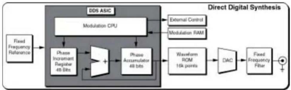
DDS DDS works by generating addresses to a waveform ROM to produce data for
a DAC. However, unlike earlier techniques, the clock is a fixed frequency reference. Instead of using a counter to generate addresses, an adder is used. On each clock cycle, the contents of a Phase Increment Register are added to the contents of the Phase Accumulator. The Phase Accumulator output is the address to the waveform ROM (see diagram below). By changing the Phase Increment the number of clock cycles needed to step through the entire waveform ROM changes, thus changing the output frequency.
Frequency changes now can be accomplished phase continuously in only one clock cycle. And the fixed clock eliminates phase jitter, requiring only a simple fixed frequency anti-aliasing filter at the output.
The DS335 uses a custom Application Specific Integrated Circuit (ASIC) to implement the address generation in a single component. The frequency resolution is equal to the resolution with which the Phase Increment can be set. In the DS335, the phase registers are 48 bits long, resulting in an impressive 1:1014 frequency resolution. The ASIC also contains a modulation control CPU that operates on the Phase Accumulator, Phase Increment, and external circuitry to allow digital synthesis and control of waveform sweeps. The Modulation CPU uses data stored in the Modulation RAM to produce frequency sweeps. All modulation parameters, such as rate, and frequency deviation, are digitally programmed.
Figure 1: Block diagram of SRS DDS ASIC
flowchart
graph TD
    A["Fixed Frequency Reference"] --> B["Phase Increment Register 48 Bits"]
    B --> C["+"]
    C --> D["Phase Accumulator 48 bits"]
    D --> E["External Control"]
    D --> F["Modulation RAM"]
    E --> G["DAC"]
    F --> G
    G --> H["Fixed Frequency Filter"]
    H --> I["Output"]
    J["DDS ASIC"] --> K["Modulation CPU"]
    K --> L["External Control"]
    K --> M["Modulation RAM"]
    N["Waveform ROM 16k points"] --> G
DDS gives the DS335 greater flexibility and power than conventional synthesizers without the drawbacks inherent in PLL designs.
DS335 Description

flowchart
graph TD
    A["10MHz Clock"] --> B["DDS345 ASIC"]
    B --> C["Waveform ROM"]
    C --> D["12 bit DAC"]
    D --> E["Cauer Filter"]
    D --> F["1 MHz Bessel Filter"]
    E --> G["Square Wave Comparator"]
    F --> G
    G --> H["Output Amp"]
    H --> I["Attenuators"]
    I --> J["Source Impedance"]
    J --> K["Function Output"]
    B --> L["Amplitude DAC"]
    L --> M["Amplitude Control"]
    M --> N["Sync Output"]
    D --> O["Modulation RAM"]
A block diagram of the DS335 is shown in Figure 2. The heart of the DS335 is a 10 MHz crystal clock. The 10 MHz clock controls the DDS ASIC, waveform ROM, and high-speed 12bit DAC. Sampling theory limits the frequency of the waveform output from the DAC to about 40% of 10 MHz, or 3 MHz. The 48 bit length of the ASIC's PIR's sets the frequency resolution to about 36 nHz. These parameters and the DAC's 12 bit resolution define the performance limits of the DS335.
The reconstruction filter is key to accurately reproducing a waveform in a sampled data system. The DS335 contains two separate filters. For sine wave generation the output of the DAC goes through a 7th order Cauer filter, while ramps, and triangles pass instead through a 3.5 MHz 5th order Bessel filter. The Cauer filter has a cutoff frequency of 3.4 MHz and a stopband attenuation of 86 dB, and includes a peaking circuit to correct for the (x)/x amplitude response characteristic of a sampled system. This filter eliminates any alias frequencies from the waveform output and allows generation of extremely pure sine waves. However, the Cauer filter has very poor time response and is only useful for CW waveforms. Therefore, the Bessel filter was chosen for its ideal time response, eliminating rings and overshoots from stepped waveform outputs.
The output from the filter passes through pre-amplifier attenuators with a 0 to 14 dB range. The attenuators are followed with a wide bandwidth power amplifier that outputs a 10 V peak-to-peak into a 50 ohm load with a rise time of less than 15 ns. The output of the power amplifier passes through a series of four step attenuators (2, 4, 8, and 16 dB) that set the DS335's final output
amplitude. The post amplifier attenuators allow internal signal levels to remain as large as possible, minimizing output noise and signal degradation.
Square waves and waveform sync signals are generated by discriminating the function waveform with a high-speed comparator. The output of the comparator passes to the SYNC OUTPUT and, in the case of square waves, to the amplifier input. Generating square waves by discriminating the sine wave signal produces a square wave output with rise and fall times much faster than allowed by either of the signal filters.
Front Panel Features
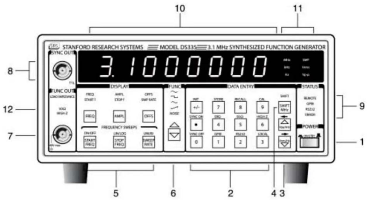
1) Power Switch The power switch turns the DS335 on and off. The DS335 has a battery backed up system RAM that remembers all instrument settings.
2) Data Entry Keys The numeric keypad allows for direct entry of the DS335's parameters. To change a parameter value simply type the new value. Entries are terminated by the UNITS keys. A typing error may be corrected by pressing the corresponding function key. For example, if the wrong numeric key is pressed while entering a new frequency, pressing the [FREQ] key will backspace over the last entered digit. If there are no digits left, the current frequency value is displayed. The [+/-] key may be selected at any time during numeric entry.
3) Units Keys The UNIT keys are used to terminate numeric entries. Simply press the key with the desired units to enter the typed value. Some parameters have no particular units and any of the unit keys may be used.
The unit keys also increase and decrease the numeric value in the DS335's display. Pressing the [UPARROW] key adds one to the flashing digit value, the [DOWN ARROW] key subtracts one from the flashing digit value. To change the position of the flashing digit, press [SHIFT] [LEFT ARROW] or [SHIFT] [RIGHT ARROW]. A few of the display menus have more than one parameter displayed at a time. The [SHIFT][LEFT ARROW] and [SHIFT][RIGHT ARROW] keys select between left and right.
4) Shift Key The shift key selects the function printed above the keys. Pressing [SHIFT] and then the desired key to select the specific function (for example [SHIFT][50Ω] sets the source impedance to 50Ω. When the SHIFT key is pressed the SHIFT LED will light. Pressing [SHIFT] a second time will deactivate shift mode.
| 5) Sweep Key These keys control the different sweep parameters including: Start and Stop Frequencies, Sweep Rate, Continuous or Single Sweep, Linear or Log Sweep, Unidirectional or Bidirectional Sweeps, and FSK. | |
| 6) Function Keys These keys control the main function output. The Func [DOWN ARROW] key and [SHIFT][UP ARROW] key select between the output functions. If the output frequency is set beyond the range allowed for a waveform (>10kHz for triangle and ramp) an error message will be displayed and the frequency will change to the maximum allowed for that function. | |
| 7) Main Function BNC | This output has an impedance of 50Ω. The shield of this output may be floated up to ±40V relative to earth ground. |
| 8) Sync Output BNC | This output is a TTL square wave synchronized to the main function output and has a 50Ω output impedance. The shield of this output may be floated up to ±40V relative to earth ground. |
| 9) Status LEDs These four LEDs indicate the DS335's status. They are: | |
| name function ____.REMOTE The DS335 is in GPIB remote state. The [3] key returns local control.GPIB Flashes on GPIB activity.RS232 Flashes on RS232 activity.ERROR Flashes on an error in the execution of a remote or local command including range errors. | |
| 10) Parameter Display | The 8 digit display shows the value of the currently displayed parameter. The LEDs below in the DISPLAY section indicate which parameter is being displayed. Error messages also appear on the display. When an error message is displayed you can return to the normal display by pressing any key. |
| 11) Units LEDs | The Units LEDs indicate the units of the displayed parameter. If no LED is lit the value has no units. The SWP LED indicates that a sweep or FSK is in progress. |
| 12) Load Impedance LEDs | These LEDs indicate the load impedance value as set by the user. The amplitude and offset display values will change according to the load impedance setting. |
Rear Panel Features

1) Power Entry Module
This contains the DS335's fuse and line voltage selector. Use a 1 amp slow blow fuse for 100/120 volt operation, and a 1/2 amp fuse for 220/240 volt operation. To set the line voltage selector for the correct line voltage, first remove the fuse. Then, remove the line voltage selector card and rotate the card so that the correct line voltage is displayed when the card is reinserted. Replace the fuse.
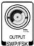
2) Sweep/FSK Output
This output generates a TTL pulse that is synchronous with the DS335's frequency sweep. When the DS335 is in FSK mode, the output voltage reflects the present frequency at the FUNCTION output BNC (TTL LOW = Start Frequency, TTL HIGH = Stop Frequency). The shield of this output is tied to that of the function output and may be floated up to ±40V relative to earth ground.
3) FSK Input
The Frequency-Shift Keying input allows the user to toggle between the start frequency and the stop frequency. The BNC takes a TTL level input. When the input is low the start frequency is active, and when the input is high the stop frequency is active. This input is sampled at 10 MHz.
4) GPIB Connector
If the DS335 has the optional GPIB/RS232 interface this connector is used for IEEE-488.1 and .2 compatible communications. The shield of this connector is connected to earth ground.
5) RS232 Connector
If the DS335 has the optional GPIB/RS232 interface this connector is used for RS232 communication. The DS335 is a DCE and accepts 8 bits, no parity, 2 stop bits at between 300 and 9600 Baud. The shield of this connector is connected to earth ground.
2-8 Features
DS335 OPERATION
Introduction
The following sections describe the operation of the DS335. The first section describes the basics of setting the function, frequency, amplitude, and offset. The second section explains sweeps and FSK. The third section explains storing and recalling setups, running self-test and autocalibration, and setting the computer interfaces.
Power-On When the power is first applied to the DS335 the unit will display its serial
number and ROM version for about three seconds. Then, the DS335 will initiate a series of self-tests of the circuitry and stored data. The test should take about three seconds and end with the message "TST PASS". If the self test fails the DS335 will display an error message indicating the nature of the problem (see the TROUBLESHOOTING section for more details). The DS335 will still attempt to operate normally after a self-test failure, pressing any key will erase the error message.
SETTING THE FUNCTION
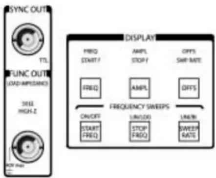
OUTPUTS The FUNCTION and SYNC BNCs are the DS335's main outputs. Both of
these outputs are fully floating, and their shields may be floated relative to earth ground by up to ±40V. Both outputs also have a 50Ω output impedance. If the outputs are terminated into high impedance instead of 50W the signal levels will be twice those programmed (the FUNCTION output may also show an increase in waveform distortion). The output impedance should be set properly from the front panel using the [SHIFT][5] or [SHIFT][6] keys. Incorrect impedance matching may result in output voltages that do not correspond to the displayed amplitudes and offsets. For example, if the DS335 is set for a 50 Ohms source impedance and the output is connected to a scope without a 50 Ohms terminator, then the scope waveform will be twice the amplitude displayed on the DS335. The programmed waveform comes from the FUNCTION output, while the SYNC output generates a TTL compatible (2.5 V into 50Ω) signal that is synchronous with the function output. The SYNC signal is suppressed if the function is set to NOISE or ARB. The SYNC signal can be disabled and enabled with the [SHIFT][0] and [SHIFT][.] keys.
FUNCTION SELECTION
The DS335's output function is selected using the FUNCTION UP/DOWN arrow keys. Simply press the keys until the desired function LED is lit. If the programmed frequency is outside of the range allowed for the selected
function, an error message will be displayed and the frequency will be set to the maximum allowed for that function.
Ramps Ramp functions usually ramp up in voltage, downward ramps may be set entering a negative amplitude (see AMPLITUDE section).
FREQUENCY To display the DS335's output frequency press the [FREQ]. The frequency
units can be Hz, kHz, or MHz, and are indicated by the LEDs on the right of the display. The DS335 has 1 Hz frequency resolution at all frequencies, for all functions. The maximum frequency depends on the function selected as shown below.
| Function Frequency Range | |
| Sine | 1 Hz → 3.100000000000 MHz |
| Square | 1 Hz → 3.100000000000 MHz |
| Triangle | 1 Hz → 10,000.000000 Hz |
| Ramp | 1 Hz → 10,000.000000 Hz |
| Noise 3.5 MHz | White Noise (fixed) |
Frequency is usually displayed by the DS335 with the highest resolution possible. However, if the frequency is below 100 Hz, the DS335 will display the frequency with 1 Hz resolution. At frequencies greater than 1 MHz the digits below 0.1 Hz cannot be displayed, but the frequency still has 1 Hz resolution and may be set via the computer interfaces.
If the function is set to NOISE the character of the noise is fixed with a band limit of 3.5 MHz. The frequency is not adjustable and the FREQ display will read "noise" instead of a numerical value.
Setting the Frequency
To set the frequency of any function simply type a new value on the keypad and complete the entry with the appropriate units (Hz, kHz, or MHz). Also, the UP and DOWN arrow keys may be used to increment or decrement the frequency by adding or subtracting one from the flashing digit.
AMPLITUDE Press [AMPL] to display the amplitude of the output function. The amplitude
may be set and displayed in units of Vpp and Vrms . The current units are indicated by the LEDs at the right of the display. The amplitude range is limited by the DC offset setting since |Vac\ peak| + |Vdc| ≤ 5 V (into 50Ω ). If the DC offset is zero the amplitude range for each of the functions is shown below:
Note: The rms value for NOISE is based on the total power in the output bandwidth (about 3.5 MHz) at a given peak to peak setting.
| Vpp Vrms | ||
| Function | Max. Min. Max. Min. | |
| Sine 10V Square | 50 mV 3.54V 0.02Vrms10V 50 mV 5.00V 0.03Vrms | |
| Triangle 10V | 50 mV 2.89V 0.01Vrms | |
| Ramp Noise | 10V 50 mV 2.89V 0.01Vrms10V 50 mV 1.62V 0.01Vrms |
50Ω Load Impedance
| Vpp Vrms | ||
| Function | Max. Min. Max. Min. | |
| Sine 20V Square 20Triangle 20Ramp 20Noise 20V | 0.1V 7.07V 0.04Vrms0.1V 10.0V 0.05Vrms0.1V 5.77V 0.03Vrms0.1V 5.77V 0.03Vrms0.1V 3.24V 0.02Vrms |
HIGH-Z Load Impedance
Output Inversion
The DS335's output may be inverted for ramp functions. This is useful for turning positive ramps into negative ramps. Entering a negative amplitude inverts the ramp output.
D.C. Only The output of the DS335 may be set to a DC level by entering an amplitude of 0 V. When the amplitude is set to zero the A.C. waveform will be completely shut off and the DS335 may be used as a DC voltage source.
DC OFFSET
When the [OFFS] key is pressed the DC offset is displayed and the Vpp indicator LED will be lit. A new value may be entered numerically with any amplitude unit key. In general, the DC offset may range between ±5V , but is restricted such that |Vac\ peak| + |Vdc| ≤ 5V (into 50 Ohms), or |Vac\ peak| + |Vdc| ≤ 10V (into HIGH-Z). The DC offset is also restricted such that |Vdc| ≤ 2 × Vpp . When the offset is changed, the output signal will briefly go to zero as the output attenuators are switched, and then back to the set offset value.
SYNC ENABLE
Pressing the [SHIFT] [.] key enables the SYNC OUT function. The [SHIFT][0] disables the output by highly attenuating the output function signal.
2-12 Function Setting
FREQUENCY SWEEPS & FSK
Introduction The DS335 can perform frequency sweeps of the sine, square, triangle, and
ramp waveforms. The sweeps may be up or down in frequency, and may be linear or logarithmic in nature. The frequency changes during the sweep are phase continuous and the sweep rate may be set between 0.01 Hz and 1000Hz. The DS335 has a SWEEP output that may be used to trigger an oscilloscope. The DS335 is also capable of Frequency-Shift Keying (FSK). FSK can be implemented either through the internal rate generator or the back panel external input to toggle between two preset frequencies.

Sweep/FSK Enable Sweeps are enabled by pressing [SHIFT][START FREQ] in the Frequency
Sweeps menu. The DS335 displays the "CONT SNGL" menu which allows the user to choose between continuous and single sweeps. The DS335 will immediately start a continuous sweep unless the user presses the UP/DOWN arrow key to select SINGLE sweep. Once a single sweep is selected, the [SHIFT][START FREQ] key triggers the sweep. If the user has selected the FSK function from the "UNI/BI" (Unidirectional/Bidirectional/FSK) menu, the single/continuous sweep option is disabled and the "FS OFF" menu appears, giving the user the choice to enable or disable the FSK function. Once the FSK function is selected and enabled, the FSK output signal appears at the Function Out BNC.
Sweep Type Pressing the [SHIFT] [STOP FREQ] key sets the sweep to either a linear or
log mode. The UP/DOWN arrow toggles between the two sweep types. The output frequency of a linear sweep changes linearly during the sweep time. The output frequency in a logarithmic sweep changes exponentially during the sweep time, spending equal time in each decade of frequency. For example, in a sweep from 1 kHz to 100 kHz, the sweep will spend half the time in the 1 kHz to 10 kHz range and half the time in the 10 kHz to 100 kHz range). It should be noted that these are digital sweeps, and that the sweep is actually composed of 1500 to 3000 discrete frequency points, depending on the sweep rate.
Sweep Waveform The type of sweep waveform may be set to UNIdirectional (ramp) or
Bldirectional (triangle) by pressing the [SHIFT][SWEEP RATE] key and then pressing the UP/DOWN arrow keys. If FSK is selected, Frequency-Shift keying is enabled and the sweeps are disabled. If the waveform is UNI (Ramp) the DS335 sweeps from the start to the stop frequency, returns to the start frequency and repeats continuously. For BI directional sweeps the DS335 sweeps from the start to the stop frequency, then sweeps from the stop frequency to the start frequency, and repeats. If the DS335 is set for a single sweep, the sweep occurs only once.
| Sweep/FSK RATE The duration of the sweep is set by [RATE], and the value is entered or modified with the keypad. The sweep rate may be set over the range of 0.01 Hz to1 kHz. The sweep rate is the inverse of the sweep time, a 0.01 Hz rate is equal to a 100s sweep time, and a1 kHz rate is equal to a 1 ms sweep time. For a TRIANGLE sweep the sweep time is the total time to sweep up and down. If FSK is selected from the UNI/BI menu, then the "Sweep Rate" button sets the FSK Rate. If the rate is set to 0 Hz then the rear panel FSK BNC input toggles between the two preset frequencies. For any non zero rate the DS335 will toggle between the two preset frequencies at the specified rate. The maximum internal FSK rate is 50 kHz. | |
| Sweep/FSK FREQUENCIES | The DS335 may sweep over any portion of its frequency range: 1 × Hz to 3.1 MHz for sine and square waves, 1 × Hz to 100 kHz for triangle and ramp waves. The sweep span is limited to six decades for logarithmic sweeps. The DS335's sweep range is set by entering the start and stop frequencies. In FSK mode, the DS335 will toggle between any two frequencies: 1 × Hz to 3.1 MHz for sine and square waves, and 1 × Hz to 100 kHz for triangle and ramp waves. There are no restrictions on the values of the start and stop frequencies for linear sweeps. |
| Start and Stop Frequencies | To enter the start and stop frequency press the [START FREQ] and [STOP FREQ] keys. The span value is restricted to sweep frequencies greater than zero and less than or equal to the maximum allowed frequency. If the stop frequency is greater than the start frequency, the DS335 will sweep up. If the start frequency is larger the DS335 will sweep down. If FSK is enabled the DS335 toggles between the Start and Stop frequencies at the Sweep/FSK Rate. If the rate has been set to zero then the rear panel FSK input is active. A TTL low level activates the start frequency and a TTL high level activates the stop frequency. |
| Sweep/FSK OUTPUT | The rear-panel SWP/FSK output is synchronous with the sweep rate. This output emits a TTL pulse at the beginning of every sweep cycle and can be used to trigger an oscilloscope. When the start frequency is selected, the Sweep output is at 0 Volts, and when the Stop frequency is selected the Sweep level is at 5 Volts. The Sweep output is synchronous with the frequency shifts. |
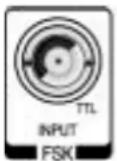  | |
| FSK Input The FSK input accepts TTL level signals. When enabled (FSK mode with 0 Hz rate), it is sampled at a 10 MHz frequency by the DS335. A low TTL level selects the start frequency, and a high TTL level selects the stop frequency (see example below). When the FSK Input is being used, the Sweep output is disabled and stays at 0 Volts. | |

line
| Frequency | FSK Input | TTL Levels | | --------- | --------- | ---------- | | 20kHz | 1 | 0 | | 10kHz | 0 | | | 20kHz | | | | 10kHz | | | | 20kHz | | | | 10kHz | | | | 20kHz | | | | Start Freq| | =20kHz | | Stop Freq | | =10kHz | | Sweep Rate| | =0Hz |External Frequency-Shift Keying (FSK) Example
INSTRUMENT SETUP
Introduction
This section describes the DS335's default settings, storing and recalling settings, setting the computer interfaces, and running self-test.
Default Settings
Press [SHIFT][+/-] to recall the DS335's default settings. The DS335's default settings are listed below:
Setting Default Value
Frequency 1 MHz
Function Sine
SYNC ON/OFF On
Load Impedance 50Ω
Display Frequency
Amplitude 1 Vpp
Offset 0.0 V
Inversion Off
Sweeps Off
Start Frequency 1Hz
Stop Frequency 3.1MHz
Trigger Source Continuous
Sweep/FSK Rate 100 Hz
Interface RS232
Baud Rate 9600
GPIB Address 22
Storing Setups
To store the DS335's current setup press [SHIFT][7] followed by a location number in the range 0 - 9. After pressing any UNITS key to enter the location number, the message "sto done" will be displayed, indicating that the settings have been stored.
Recalling Stored Settings
To recall a stored setting press [SHIFT][8] followed by a location number in the range 0 - 9. After pressing any UNITS key to enter the location number the message "rcl done" will be displayed, indicating that the settings have been recalled. If nothing is stored in the selected location, or the settings are corrupted, the message "rcl err" will be displayed.
GPIB Setup To set the DS335's GPIB interface press [SHIFT][1]. The GPIB enable
selection will be displayed. Use the [UP ARROW] and [DOWN ARROW] keys to enable the GPIB interface. Press [SHIFT][1] again to display the GPIB address. Enter the address desired using the numeric keypad or arrow keys. The range of valid addresses is 0 - 30.
NOTE: If the DS335 does not have the optional GPIB/RS232 interfaces the message "no GPIB" will be displayed when the GPIB menu is accessed. Only one of the GPIB and RS232 interfaces may be active at a given time, the RS232 interface is automatically disabled when GPIB is enabled.
| RS232 Setup To set the DS335's RS232 interface press [SHIFT][2]. The RS232 enable selection will be displayed. Use the UP/DOWN ARROW keys to enable the RS232 interface. Press [SHIFT][2] again to display the RS232 baud rate selection. The available baud rates of 300, 600, 1200, 2400, 4800, or 9600 baud can be set with the UP/DOWN ARROW keys. | |
| NOTE: If no interface option is present the message "no RS232" will be displayed when the RS232 menu is accessed. Only one of the GPIB and RS232 interfaces may be active at a given time, the GPIB interface is automatically disabled when RS232 is enabled. | |
| User Service Requests | While the GPIB is enabled the user may issue a service request (SRQ) by pressing [SHIFT][4]. The message "srq sent" will be displayed, and the GPIB LED will light. The GPIB LED will go off after the host computer does a serial poll of the DS335. Note: the user service request is in addition to the usual service requests based on status conditions (see PROGRAMMING section for details). |
| Communications Data | Press [SHIFT][2] three times to display the last 256 characters of data that have been received by the DS335. This display is a 3 character window into the DS335's input data queue that could be scrolled to view the previous 256 characters. The data is displayed in ASCII hex format, with each input character represented by 2 hexadecimal digits. The most recently received character has a decimal point indicator. Pressing [DOWN ARROW] scrolls the display to the beginning of the queue, and [UP ARROW] scrolls to later in the queue. |
| AUTO-TEST | |
| Introduction | The DS335 has a built-in test routine that allows the user to test a large portion of instrument functionality quickly and easily. Self-test starts every time the DS335 is turned ON. |
| SELF-TEST The DS335's self-test is always executed on power-up. The test checks most of the digital circuitry in the DS335, and should end with the display "test pass". If the self-test encounters a problem it will immediately stop and display a warning message. See the TROUBLESHOOTING section for a list and explanation of the error messages. If the DS335 fails its test it still may be operated. | |
| The DS335 tests its CPU and data memory, ROM program memory, calibration constant integrity, the computer interfaces, and the modulation program memory | |
| Items not tested are the connections from the PC boards to the BNC connectors, the 12-bit waveform DAC, the output amplifier, the offset and amplitude control circuits, and the output attenuators. | |
| CALIBRATION BYTES | It is possible to recall and modify the DS335 factory calibration bytes. Please refer to the Test and Calibration Chapter for more detail. |
| The DS335 Function Generator may be remotely programmed via either the RS232 or GPIB (IEEE-488) interfaces. Any computer supporting either of these interfaces may be used to program the DS335. Only one interface is active at a time. All front and rear panel features (except power) may be controlled. | |
| GPIB Communications | The DS335 supports the IEEE-488.1 (1978) interface standard. It also supports the required common commands of the IEEE-488.2 (1987) standard. Before attempting to communicate with the DS335 over the GPIB interface, the DS335's device address must be set. The address is set in the second line of the GPIB menu (type [SHIFT][1] twice), and may be set between 0 and 30. The default address is 22. |
| RS232 Communications | The DS335 is configured as a DCE (transmit on pin 3, receive on pin 2) and supports CTS/DTR hardware handshaking. The CTS signal (pin 5) is an output indicating that the DS335 is ready, while the DTR signal (pin 20) is an input that is used to control the DS335's transmitting. If desired, the handshake pins may be ignored and a simple 3 wire interface (pins 2, 3 and 7) may be used. The RS232 interface baud rate may be set in the second line of the RS232 menu (type [SHIFT][2] twice). The interface is fixed at 8 data bits, no parity, and 2 stop bits. |
| Front Panel LEDs | To assist in programming, the DS335 has 4 front panel status LEDs. The RS232 and GPIB LEDs flash whenever a character is received or sent over the corresponding interface. The ERROR LED flashes when an error has been detected, such as an illegal command, or an out of range parameter. The REMOTE LED is lit whenever the DS335 is in a remote state (front panel locked out). |
| Data Window To help find program errors, the DS335 has an input data window which displays the data received over either the GPIB or RS232 interfaces. This window is activated by typing [SHIFT][2] or [SHIFT][1] three times. The menu displays the received data in hexadecimal format. The last 256 characters received can be scrolled through using the MODIFY up/down arrow keys. A decimal point indicates the most recently received character. | |
| Command Syntax Communications with the DS335 use ASCII characters. Commands may be in either UPPER or lower case and may contain any number of embedded space characters. A command to the DS335 consists of a four character command mnemonic, arguments if necessary, and a command terminator. The terminator may be either a carriage returnor linefeedon RS232, or a linefeedor EOI on GPIB. No command processing occurs until a command terminator is received. All commands function identically on GPIB and RS232. Command mnemonics beginning with an asterisk "" are IEEE-488.2 (1987) defined common commands. These commands also function identically on RS232. Commands may require one or more parameters. Multiple parameters are separated by commas ";".Multiple commands may be sent on one command line by separating them by semicolons ";". The difference between sending several commands on the same line and sending several independent commands is that when a command line is parsed and executed the entire line is executed before any other device action proceeds. | |
There is no need to wait between commands. The DS335 has a 256 character input buffer and processes commands in the order received. If the buffer fills up the DS335 will hold off handshaking on the GPIB and attempt to hold off handshaking on RS232. If the buffer overflows the buffer will be cleared and an error reported. Similarly, the DS335 has a 256 character output buffer to store output until the host computer is ready to receive it. If the output buffer fills up it is cleared and an error reported. The GPIB output buffer may be cleared by using the Device Clear universal command.
The present value of a particular parameter may be determined by querying the DS335 for its value. A query is formed by appending a question mark "?" to the command mnemonic and omitting the desired parameter from the command. If multiple queries are sent on one command line (separated by semicolons, of course) the answers will be returned in a single response line with the individual responses separated by semicolons. The default response terminator that the DS335 sends with any answer to a query is carriage return-linefeed
Examples of Command Formats
FREQ, 1000.0
FREQ?
*IDN?
*TRG
FUNC 1 ;FUNC?
Programming Errors The DS335 reports two types of errors that may occur during command execution: command errors and execution errors. Command errors are errors in the command syntax. For example, unrecognized commands, illegal queries, lack of terminators, and non-numeric arguments are examples of command errors. Execution errors are errors that occur during the execution of syntactically correct commands. For example, out of range parameters and commands that are illegal for a particular mode of operation are classified as execution errors.
No Command Bit The NO COMMAND bit is a bit in the serial poll register that indicates that there are no commands waiting to be executed in the input queue. This bit is reset when a complete command is received in the input queue and is set when all of the commands in the queue have been executed. This bit is useful in determining when all of the commands sent to the DS335 have been executed. This is convenient because some commands, such as setting the function or sweep, take a long time to execute and there is no other way of determining when they are done. The NO COMMAND bit may be read while commands are being executed by doing a GPIB serial poll. There is no way to read this bit over RS232. Note that using the *STB? query to read this bit will always return the value 0 because it will always return an answer while a command is executing- the *STB? command itself!
DETAILED COMMAND LIST The four letter mnemonic in each command sequence specifies the command. The rest of the sequence consists of parameters. Multiple
parameters are separated by commas. Parameters shown in {} are optional or may be queried while those not in {} are required. Commands that may be queried have a question mark in parentheses (?) after the mnemonic. Commands that may ONLY be queried have a ? after the mnemonic. Commands that MAY NOT be queried have no ?. Do not send () or {} as part of the command.
All variables may be expressed in integer, floating point or exponential formats (i.e., the number five can be either 5, 5.0, or .5E1). The variables i and j usually take integer values, while the variable x take real number values.
Function Output Control Commands
AECL The AECL command sets the output to the ECL levels of 1 V peak-to-peak with a -1.3 V offset. That is, from -1.8V to -0.8V.
AMPL (?) x The AMPL command sets the output amplitude to x. The value x must
consist of the numerical value and a units indicator. The units may be VP (Vpp) or VR (Vrms). For example, the command AMPL 1.00VR will set the output to 1.0 Vrms. Note that the peak AC voltage (Vpp/2) plus the DC offset voltage must be less than 5 Volts (for 50Ω source). Setting the amplitude to 0 Volts will produce a DC only (no AC function) output controlled by the OFFS command.
The AMPL? query will return the amplitude in the currently displayed units. For example, if the display is 3.0 Vrms the AMPL? query will return 3.0VR. If a units indicator is sent with the AMPL? query (such as, AMPL? VP) the displayed units will be changed to match the units indicator and the amplitude returned in those units.
ATTL The ATTL command sets the TTL output levels of 5V peak-to-peak with a 2.5V offset. That is, from 0V to 5V.
FREQ (?) x The FREQ command sets the output frequency to x Hertz. The FREQ?
query returns the current output frequency. The frequency is set and returned with 1 × Hz resolution. If the current waveform is NOISE an error will be generated and the frequency will not be changed.
FUNC (?) i The FUNC command sets the output function type to i. The correspondence
of i and function type is shown in the table below. If the currently selected frequency is incompatible with the selected function an error will be generated and the frequency will be set to the maximum allowed for the new function. The FUNC? query returns the current function.
| i Function | ||||||||
| 0 | S | I | N | E | ||||
| 1 | S | Q | U | A | R | E | ||
| 2 | T | R | I | A | N | G | L | E |
| 3 | R | A | M | P | ||||
| 4 NOISE | ||||||||
INVT (?) i The INVT command turns output inversion on (i=1) and off (i=0). The INVT?
query returns the current inversion status. This function is used with the ramp waveform to set it for positive or negative slope.
| KEYS(?)i The KEYS command simulates the pressing of a front panel key. The KEYS? query returns the keycode of the most recently pressed key.Keycodes are assigned as follows: | |
| Key Name Key Code | |
| FREQ 1 | |
| AMPL 2 | |
| OFFSET 3 | |
| START FREQ 4 | |
| STOP FREQ 5 | |
| SWEEP RATE 6 | |
| 0 7 | |
| 1 | 8 |
| 2 | 9 |
| 3 | 10 |
| Vrms/HZ/DOWN 11 | |
| SEL FNC 12 | |
| Decimal Point 13 | |
| 4 | 14 |
| 5 | 15 |
| 6 | 16 |
| Vpp/kHz/UP 17 | |
| +/- | 19 |
| 7 | 20 |
| 8 | 21 |
| 9 | 22 |
| MHz/SHIFT | 23 |
| OFFS (?) x | The OFFS command sets the output's DC offset to x volts. The OFFS? query returns the current value of the DC offset. The DC offset voltage plus the peak AC voltage must be less than 5 Volts (into 50Ω). |
SYNC(?)I Turns the SYNC output on (i=1) or off (i=0).
| TERM(?) i | Sets the output source impedance to 50Ω (i=0), or hi-Z (i=1). The TERM? query returns the current source impedance setting. Note that all amplitude and offset display settings get doubled when switching from 50 Ohm to High Impedance. Similarly, when switching from high impedance to 50 Ohm all amplitude and offset display values get halved. The actual BNC output is not affected by this change. |
Sweep & FSK Control Commands
note: All sweep & FSK parameters may be set at any time. For the changes to have an effect be sure that the sweep or FSK type is set correctly and that sweep or FSK is enabled (see the STYP and SWEN commands).
| FSEN(?) i | Enables FSK on (i=1) or off (i=0). This function is valid only if FSK has been selected with the SDIR command (SDIR2) or from the front panel. If the FSK rate has been set between 0.01Hz and 50 kHz then the FSK starts following the "FSEN1" command. If the rate has been set to 0Hz and FSK selected, the command "FSEN1" would enable the FSK BNC input on the rear panel. This TTL signal is sampled at a 10MHz rate and toggles between the Start frequency and the Stop frequency. |
*TRG The *TRG command triggers a single sweep. The trigger source must be set to SINGLE (see the TSRC command below).
SDIR(?)i Sets the sweep direction. 0 = Ramp (unidirectional), 1 = Triangle (bidirectional), 2 = enable FSK (disable sweeps).
STYP (?) i The STYP command sets the sweep type to i. The correspondence of i to type is shown in the table below. The STYP? query returns the current sweep type. Refer to the SDIR command for sweep direction.
i Waveform 0 LIN SWEEP 1 LOG SWEEP
SPFR (?) x The SPFR command sets the sweep stop frequency to x Hertz. An error will be generated if the sweep frequency is less than or equal to zero or greater than allowed by the current function. The SPFR? query returns the current sweep stop frequency. If the stop frequency is less than the start frequency (the STFR command) a downward sweep from maximum to minimum frequency will be generated. The stop frequency is also used in the FSK mode.
SRAT (?) x The SRAT command sets the trigger rate for internally triggered single sweeps and FSK to x Hertz. x is rounded to two significant digits and may range from 0.01 Hz to 1 kHz for sweeps and 0.01Hz to 50kHz for FSK. The SRAT? query returns the current trigger rate. If the rate is set to 0Hz and FSK is enabled (SDIR = 2) then the external FSK BNC is used to toggle between the start and stop frequencies.
STFR (?) x The STFR command sets the sweep start frequency to x Hertz. An error will be generated if the sweep frequency is less than or equal to zero or greater than allowed by the current function. The STFR? query returns the current sweep start frequency. If the start frequency is greater than the stop frequency (the SPFR command) a downward sweep from maximum to minimum frequency will be generated. The stop frequency is also used in the FSK mode.
SWEN(?) i Enables sweeps on (i=1) or off (i=0). If the continuous sweep is selected, enabling sweeps will start the sweep with the specified rate. If triggered single sweep is selected and sweeps are enabled then the DS335 waits for a front panel trigger or a *TRG command to start the sweep.
TSRC (?) i The TSRC command sets the trigger source for sweeps to i. The correspondence of i to source is shown in the table below. The TSRC? query returns the current trigger source.
i Waveform 0 SINGLE 1 INTERNAL RATE
For single sweeps the *TRG command triggers the sweep.
Setup Control Commands
*IDN? The *IDN common query returns the DS335's device configuration. This
string is in the format: StanfordResearchSystems, DS335, serial number, version number. Where "serial number" is the five digit serial number of the particular unit, and "version number" is the 3 digit firmware version number.
*RCL i The *RCL command recalls stored setting number i, where i may range from
0 to 9. If the stored setting is corrupt or has never been stored an execution error will be generated.
*RST The *RST common command resets the DS335 to its default configurations.
*SAV i The *SAV command saves the current instrument settings as setting number i.
Status Reporting Commands
(See tables at the end of the Programming section for Status Byte definitions.)
*CLS The *CLS common command clears all status registers. This command does not affect the status enable registers.
*ESE (?) i The *ESE command sets the standard event status byte enable register to the decimal value i.
*ESR? {i} The *ESR common command reads the value of the standard event status register. If the parameter i is present the value of bit i is returned (0 or 1). Reading this register will clear it while reading bit i will clear just bit i.
*PSC (?) i The *PSC common command sets the value of the power-on status clear bit. If i = 1 the power on status clear bit is set and all status registers and enable registers are cleared on power up. If i = 0 the bit is cleared and the status enable registers maintain their values at power down. This allows the production of a service request at power up.
*SRE (?) i The *SRE common command sets the serial poll enable register to the decimal value of the parameter i.
*STB? {i} The *STB? common query reads the value of the serial poll byte. If the parameter i is present the value of bit i is returned (0 or 1). Reading this register has no effect on its value as it is a summary of the other status registers.
DENA (?) i The DENA command sets the DDS status enable register to the decimal value i.
STAT? {i} The STAT? query reads the value of the DDS status byte. If the parameter i is present the value of bit i is returned. Reading this register will clear it while reading bit i will clear just bit i.
Hardware Test and Calibration Commands
NOTE: These commands are primarily intended for factory calibration use and should never be needed during normal operation. Incorrect use of some of these commands can destroy the calibration of the DS335.
\CLK? The \CLK? command queries the DS335 for the status of its calibration jumper. Shown below are the different status values that the DS335 can return:
Status value Meaning 0 Calibration disabled 1 Calibration enabled
FCL The FCL command recalls the factory calibration bytes. This command will generate an error if calibration is not enabled.
*TST? The *TST? common query runs the DS335 internal self-tests. After the tests are complete the test status is returned. The status may have the following values (see the TROUBLESHOOTING section for more details):
Status value Meaning
0 No Error.
1 CPU Error. The DS335 has detected a problem in its CPU.
2 Code Error. The DS335's ROM firmware has a checksum error.
3 Sys RAM Error. The system RAM failed its test.
4 Cal Data Error. The DS335's calibration data has become corrupt.
5 Unused.
6 Program Data Error. The modulation program RAM failed its test.
7 DS335 not warmed up. At least 2 minutes must elapse between power on and calibration.
PRE (?) i The \PRE command sets the DS335's pre-amplifier attenuators to range i. The integer i is the attenuation value in dB and ranges from 0 to 14 in increments of two. Resetting the amplitude will return the attenuators to their normal position. The \PRE? query returns the current attenuator position.
PST (?) i The PST command sets the DS335's post-amplifier attenuators to range i . The integer i is the attenuation value in dB and ranges from 0 to 30 in increments of two. Resetting the amplitude will return the attenuators to their normal position. The PST? query returns the current attenuator position .
\WRD (?) j,k The \WRD command sets the value of calibration word j to k. Parameter j may have a value from 0 to 554, while k may range from -127 to +65535. This command will generate an error if calibration is not enabled. NOTE: this command will alter the calibration of the DS335. To correct the calibration the factory calibration bytes may be recalled (see the \$FCL command). The calibration bytes cannot be altered unless the warm-up bit has been set.
STATUS BYTE DEFINITIONS
Status Reporting
The DS335 reports on its status by means of three status bytes: the serial poll byte, the standard status byte, and the DDS status byte.
On power on the DS335 may either clear all of its status enable registers or maintain them in the state they were in on power down. The action taken is set by the *PSC command and allows things such as SRQ on power up.
Serial Poll Status Byte:
bit name
usage
0 Sweep Done set when no sweeps are in progress
1 Sweep Enable set when sweep is enabled
2 User SRQ set if the user sends a SRQ from the front panel
3 DDS An unmasked bit in the DDS status register has been set.
4 MAV The gpib output queue is non-empty
5 ESB An unmasked bit in the standard status byte has been set.
6 RQS/MSS SRQ (Service Request)bit.
7 No Command There are no unexecuted commands in the input queue
The DDS and ESB bits are set whenever any unmasked bit (bit with the corresponding bit in the byte enable register set) in their respective status registers is set. They are not cleared until the condition which set the bit is cleared. Thus, these bits give a constant summary of the enabled status bits. A service request will be generated whenever an unmasked bit in the serial poll register is set. Note that service requests are only produced when the bit is first set and thus any condition will only produce one service request. Accordingly, if a service request is desired every time an event occurs the status bit must be cleared between events.
Standard Event Status Byte:
bit name
usage
0 unused
1 unused
2 Query Error Set on output queue overflow
3 unused
4 Execution err Set by an out of range parameter, or non-completion of some command due to a condition such as an incorrect waveform type.
5 Command err Set by a command syntax error, or unrecognized command
6 URQ Set by any key press
7 PON Set by power on
This status byte is defined by IEEE-488.2 (1987) and is used primarily to report errors in commands received over the communications interfaces. The bits in this register stay set once set and are cleared by reading them or by the *CLS command.
DDS Status Byte:
bit name
usage
0 Trig'd Set when a sweep is triggered.
1 Trig Error Set when a trigger rate error occurs.
2 Unused
3 Unused
4 Warmup Set after the warmup period has expired.
5 Test Error Set if a self test error occurs.
6 Unused
7 mem err the stored setting were corrupt on power up.
The Warmup bit will be set and remain set after the warmup period has expired. The rest of the bits in this register are set when the corresponding event occurs and remain set until cleared by reading this status byte or by the *CLS command.
Program Examples
Introduction The following examples demonstrate interfacing the DS335 via RS232 and
the GPIB interface using the National Instruments GPIB card. Using a different brand of card would be similar except for the program lines that actually send the data. These examples are intended to demonstrate the syntax of the DS335's command set.
To successfully interface the DS335 to a PC via the GPIB interface, the instrument, interface card, and interface drivers must all be configured properly. To configure the DS335, the GPIB address must be set in the GPIB menu. The default GPIB address is 22; use this address unless a conflict occurs with other instruments in your system.
Make sure that you follow all the instructions for installing the GPIB card. The National Instruments card cannot be simply unpacked and put into your computer. To configure the card you must set jumpers and switches on the card to set the I/O address and interrupt levels. You must run the program "IBCONF" to configure the resident GPIB driver for your GPIB card. Please refer to the National Instruments manual for information. In this example, the following options must be set with IBCONF:
Device name: dds335
Device address: 22
EOS character: 0Ah (linefeed)
Once all the hardware and GPIB drivers are configured, use "IBIC". This terminal emulation program allows you to send commands to the DS335 directly from your computer's keyboard. If you cannot talk to the DS335 via "IBIC", then your programs will not run.
Use the simple commands provided by National Instruments. Use "IBWRT" and "IBRD" to write and read from the DS335. After you are familiar with these simple commands, you can explore more complex programming commands.
The RS232 program assumes the RS232 option is enabled ([SHIFT][2]) and the BAUD rate is set to 9600 BAUD.
The GPIB example was written in C and the RS232 example was written in BASIC.
EXAMPLE 1: GPIB COMMUNICATION. C LANGUAGE
This program communicates with the DS335 via GPIB. The program is written in C.
/*
C Program to demonstrate communication with the DS335 via
GPIB. Written in Microsoft C and uses National Instruments
GPIB card. Assumes DS335 is installed as device name DDS335.
Refer to National Instruments for Device Name setup.
*/

#include <stdio.h>
#include <string.h>
#include <stdlib.h>
#include <dos.h>

#include <decl.h> /* National Instruments header files */

void main(void); /* function declaration */

int dds335;

void main()
{
    char cmd[40];
    char start[20];
    char stop[20];

    if ((dds335 = ibfind("DDS335")) < 0) /* open National driver */
    {
    printf ("Cannot find DDS335\n");
    exit(1);
    }

    /* Now that the driver is located, reset the DS335 */

    sprintf (cmd, "*RST\n");
    ibwrt(dds335, cmd, strlen(cmd)); /* send command */

    /* Setup the DS335 as follows:
    500 kHz Square Wave, 1.5 Vpp, -1.0 Volt offset, display offset */

    sprintf (cmd, "FREQ500000; AMPL1.5VP; OFFS-1.0; KEYS3;\n");
    ibwrt(dds335, cmd, strlen(cmd)); /* send commands */

    /* Now query the DS335 for the sweep start and stop frequencies */

    sprintf (cmd, "STFR?\n"); /* ask for start rate */
    ibwrt (dds335, cmd, strlen(cmd)); /* send query */
    ibrd(dds335, start, 20); /* read back start frequency */

    sprintf (cmd, "SPFR?\n"); /* ask for stop rate */
    ibwrt (dds335, cmd, strlen(cmd)); /* send query */
    ibrd(dds335, stop, 20); /* read back stop frequency */

    printf("\n\n\n\n ***** DS335 Setup Demo *****");
    printf("\n\n\n\nDS335 Sweep Start Frequency = %e Hz\n\n", atof(start));
    printf("DS335 Sweep Stop Frequency = %e Hz\n", atof(stop));
}
EXAMPLE 2: RS232 COMMUNICATION. BASIC LANGUAGE
BASIC Program to demonstrate communication with the DS335 via RS232. Program assumes the RS232 option is enabled (use [SHIFT] [2]) and the BAUD rate is set to 9600.
10 OPEN "com2:9600,n,8,2,cs,ds,cd" FOR RANDOM AS #1 'Set up com2'
20 PRINT #1, " "
30 PRINT #1, "*rst" 'Reset the DS335'
40 GOSUB 190 'Query DS335 and display result'
50 PRINT #1, "freq1234567" 'Set new frequency'
60 GOSUB 190 'Query DS335 and display result'
70 PRINT #1, "*rst" 'Reset the DS335'
80 FOR I = 0 TO 4 'Step through all functions'
90 PRINT #1, "func", I
100 GOSUB 190 'Query DS335 and display result'
110 NEXT I
120 PRINT #1, "*rst" 'Reset the DS335'
130 PRINT #1, "ampl 0vp" 'Set amplitude to 0 volts'
140 FOR I = -5 TO 5 'Set DS335 offset from -5V to +5V'
150 PRINT #1, "offs", I 'and query each time'
160 GOSUB 190 'Query DS335 and display result'
170 NEXT I
180 END
'Routine to query the DS335 frequency,'
190 PRINT #1, "freq?" 'offset, and amplitude and display them'
200 INPUT #1, F
210 PRINT #1, "ampl?"
220 INPUT #1, A
230 PRINT #1, "offs?"
240 INPUT #1, O
250 PRINT " Frequ="; F; " Ampl="; A; " Offs="; O
260 RETURN
TROUBLESHOOTING
If Nothing Happens on
Power On Make sure that the power entry module on the rear panel is set for the proper
ac line voltage for your location, that the correct fuse is installed, and that the line cord is inserted all the way into the power entry module. The selected line voltage may be seen through the clear window, just below the fuse.
When the unit is plugged in and turned "ON", the unit's firmware version number and serial number will be briefly displayed. Then the self tests should execute.
Cold Boot
If the unit displays no sensible message, the "cold boot" procedure may fix the problem. To do a "cold boot", turn the unit off. Then, while holding the "+/-" button, turn the unit "ON". This procedure initializes the RAM and recalls all factory calibration values.
ERROR MESSAGES
The following lists explain all of the error messages that the DS335 can generate. The messages are divided into operational errors, errors in using the instrument, and self-test errors. The messages are listed alphabetically.
Operational Errors These error messages may appear during normal front panel operation and generally are warnings of illegal parameter entries.
Message Meaning
AC Error Amplitude entered is out of allowable range.
AC-DC Error The output |V
ac| + |Vdc| > 5V. Adjust either the offset or amplitude.
Freq Error Attempt to set output frequency outside of range allowed for current function, ≤ 0 Hz or >3.1 MHz, or attempting to set frequency for NOISE function.
No GPIB Cannot access GPIB menus if option board is not installed.
No RS232 Cannot access RS232 menus if option board is not installed.
Off Error
DC output offset outside of ±5V range (into 50Ω).
Out q err Output queue error. The DS335 output queue is full due to too many queries that have not been read back.
Range Er Parameter in command is out of allowed range for that command.
Rate Err Sweep rate out of range (0.01 Hz to 1kHz).
Rcl Err Parameter memory corrupt on power up, stored setting corrupt. Not a worry unless this error occurs frequently. Check the battery if so.
Span Err Logarithmic sweep span error. The start and stop frequencies are apart by more than six decades.
StrtF Er
The sweep start frequency is out of range (0 < Freq ≤ max for function).
Stop F Er
The sweep stop frequency is out of range (0 < Freq ≤ max for function).
Syn Err The command syntax is invalid. See PROGRAMMING section for correct command syntax.
UART Error The DS335 has detected an error on its computer interface option board.
Uni Err The units set with AMPL command are not V
pp, or Vrms .
Self-Test Errors
These errors may occur during the DS335's self-test. In general, these messages indicate DS335 hardware problems. If the errors occur repeatedly the unit may have an electrical problem. The messages are listed alphabetically, also listed is the status value returned by the *TST? command.
Message Status Value Meaning
Cald Err 4 The RAM calibration data has become corrupt. The factory values will be reloaded from ROM. This message is not a problem unless it occurs frequently, which could indicate a problem with the battery backup circuits.
Code Err XX 2 The DS335's ROM has a checksum error. XX is the checksum value.
CPU Error 1 The DS335 has detected a problem in its Z80 CPU.
Prgd Err 6 Read/write test of modulation RAM (U400) failed. Can be bad RAM, ASIC, or bus problem.
Sysd Err 3 CPU RAM (U206) failed read/write test.
Cal Dly Err 7 The DS335 is not warmed up. Wait until warmed up for at least two minutes before starting autocal.
GPIB PROBLEMS
First, make sure that the GPIB interface is enabled. Press [SHIFT][1] to display the enable status line. GPIB should be "ON". If not, turn GPIB on using the UP/DOWN ARROW keys. Second, the GPIB address of the DS335 must be set to match that expected by the controlling computer. The default GPIB address is 22, and so it is a good idea to use this address when writing programs for the DS335. Any address from 0 to 30 may be set in the GPIB menu. To check the GPIB address, press [SHIFT][1] twice to view the GPIB address. The entry keys or the UP/DOWN ARROW keys may be used to set the GPIB address.
The DS335 will ignore its front panel key pad when Remote Enable (REN) has been asserted by the GPIB. This "REMOTE" state is indicated by the REMOTE LED. To return to LOCAL operation (ie. to enable the front panel) press [3]. Controlling programs may inhibit the ability to return to LOCAL operation by asserting the Local-Lockout state (LLO).
A linefeed character is sent with and End or Identify (EOI) to terminate strings from the DS335. Be certain that your GPIB controller has been configured to accept this sequence.
RS-232 PROBLEMS
First, make sure that the RS232 interface is enabled. Press [SHIFT][2] to display the enable status line. RS232 should be "ON". If not, turn RS232 on using the UP/DOWN ARROW keys. Second, the RS-232 baud rate must be set to match that expected by the controlling computer. The default baud
rate is 9600 baud. The DS335 always sends two stop bits, 8 data bits, and no parity, and will correctly receive data sent with either one or two stop bits.
When connecting to a PC, use a standard PC serial cable, not a "null-modem" cable. The DS335 is a DCE (Data Communications Equipment) device, and so should be connected with a "straight" cable to a DTE device (Data Terminal Equipment). The "minimum" cable will pass pins 2,3 and 7. For hardware handshaking, pins 5 and 20 (CTS and DTR) should be passed. Occasionally, pins 6 and 8 (DSR and CD) will be needed: these lines are always asserted by the DS335.
PERFORMANCE TESTS
INTRODUCTION
The procedures in this section test the performance of the DS335. The first set tests the basic functionality of the DS335 from the front panel. The second set of tests actually measures the DS335's specifications. The results of each test may be recorded on the test sheet at the end of this section.
NECESSARY EQUIPMENT
The following equipment is necessary to complete the tests. The suggested equipment or its equivalent may be used.
Instrument Critical Specifications
Recommended Model
Analog Oscilloscope 350 MHz Bandwidth Tektronix 2465
Time Interval Counter Frequency Range: 20 MHz minimum SRS SR620
Time Interval Accuracy: 1ns minimum
FFT Spectrum Analyzer Frequency Range: DC to 100 kHz SRS SR760
Amplitude Accuracy: ±0.2 dB
Distortion: < 75 dB below reference
RF Spectrum Analyzer Frequency Range: 1 kHz to 100 MHz Anritsu MS2601/HP4195A
Amplitude: ±0.5 dB
Distortion and Spurious: < -70 dB
DC/AC Voltmeter 5 1/2 Digit DC accuracy Fluke 8840A
True RMS AC to 100 kHz
Thermal Converter
Input Impedance: 50Ω
Input Voltage: 3 Vrms
Frequency: DC to 10 MHz
Accuracy: ±0.05dB
10 MHz Frequency Standard
Frequency: 10 MHz ± .001 ppm
Phase Noise: < -130 dBc @ 100Hz
Ballantine 1395A-3
50Ω Terminator
50Ω ± 0.2 %, 1 Watt
HP 11048C
Doubly Balanced Mixer
Impedance: 50Ω
Frequency: 1 - 20 MHz
Mini-Circuits ZAD-3SH
FUNCTIONAL TESTS
These simple tests verify that the DS335's circuitry is functional. They are not intended to verify the DS335's specifications.
| Front Panel Test | This test verifies the functionality of the front panel digits, LED's, and buttons. |
| 1) Turn on the DS335 while holding down [FREQ]. Press the [UP ARROW] and a single segment of the leftmost digit should light. | |
| 2) Use [DOWN ARROW] to light each segment (7 of them) and the decimal point of the left most two digits. Only a single segment should be on at a time. [UP ARROW] will step backward through the pattern. | |
| 3) Push the down arrow key again and all of the segments of all 8 digits should light. | |
| 4) Press the down arrow key repeatedly to light each front panel indicator LED in turn, top to bottom, left to right. At any time only a single LED should be on. | |
| 5) After all of the LEDs have been lit further pressing of the front panel keys will display the key code associated with each key. Each key should have a different keycode. | |
| Internal Self-Tests | The internal self tests test the functionality of the DS335 circuitry. |
| 1) Turn on the DS335. The ROM firmware version number, and the serial number should be displayed for about 3 seconds. The self tests will execute and the message "TEST PASS" should be displayed. If an error message appears see the TROUBLESHOOTING section for a description of the errors. | |
| Sine Wave | This procedure visually checks the sine wave output for the correct frequency and any visible irregularities. |
| 1) Connect the DS335's output to the oscilloscope input and terminate in 50Ω. | |
| 2) Set the DS335 to sine, 1 MHz, 10 Vpp, and 50Ω Load Impedance. Set the scope to 2 V/div vertical, and .1us/div horizontal. | |
| 3) The scope should display a sine wave with one cycle per horizontal division and about five divisions peak-to-peak. There should be no visible irregularities in the waveform. | |
| Square Wave This procedure checks the square wave output for frequency, rise time, and aberrations. | |
4) Increase the scope sensitivity to 1V/div and measure the size of the overshoot at the beginning of the square wave. It should be less than 0.2V peak-to-peak.
5) Adjust the scope to 2V/div and 5ns/div. Measure the 10% to 90% rise time of the square wave. It should be less than 20ns.
This test provides a visual indication of the sine wave amplitude flatness.
1) Connect the DS335's output to the oscilloscope input and terminate in 50Ω.
2) Set the DS335 to sine wave, 10Vpp, and 50Ω Load Impedance. Set to linear sweep with a Unidirectional waveform. Set the start frequency to 1Hz, stop frequency to 3MHz, and the rate to 100Hz. Turn the DS335's sweep ON.
3) Set the scope to 2V/div vertical, and 1ms/div horizontal. Trigger the scope on the falling edge of the DS335's SWEEP output (Rear Panel).
4) The scope should show a sweep that is essentially flat. The peak-to-peak variations should be less than ±1.2% . Ignore any dc variations, using the peak-to-peak measurements for flatness comparison.
Amplitude Flatness
Output Level This test provides a visual check of the DS335's output level control.
1) Connect the DS335's output to the oscilloscope input and terminate in 50Ω.
2) Set the DS335 to sine wave, 1MHz, 10Vpp, and 50Ω Load Impedance. Set the scope to 2V/div vertical and 1×s/div horizontal.
3) Verify that the DS335's output is about 10V pk-to-pk.
4) Set the DS335 to 5Vpp verify the output.
5) Repeat step 4 at 1Vpp, 0.5 Vpp, 0.1 Vpp, and 0.05 Vpp. Adjust the scope as necessary.
THIS COMPLETES THE FUNCTIONAL TESTS
PERFORMANCE TESTS
These tests are intended to measure the DS335's conformance to its published specifications. The test results may be recorded on the test sheet at the end of this section. Allow the DS335 at least 1/2 hour to warm up, run the DS335's self test procedure, and proceed with the tests.
FREQUENCY ACCURACY
This test measures the accuracy of the DS335's frequency. If the frequency is out of specification the DS335's timebase frequency should be adjusted (see CALIBRATION section).
Tolerance: ± 50 ppm of selected frequency
1) Turn the DS335 on and allow it to warm up for at least 1/2 hour. Set the DS335 for sine wave, 1 MHz, 1 Vpp, and 50Ω Load Impedance.
2) Attach the output of the DS335 to the frequency counter. Terminate into 50Ω. Attach the reference frequency input of the counter to the frequency standard. Set the counter for a 1s frequency measurement.
3) The counter should read 1MHz ± 50Hz. Record the result.
AMPLITUDE ACCURACY
The following tests measure the accuracy of the DS335 output amplitude. There are separate tests for sine, square, and ramp/triangle. The tests measure the accuracy of the amplitude as a function of frequency. The sine wave test also measures the performance of the attenuators. There is only a single test for triangle and ramp functions because they have the same signal path.
Frequency < 100 kHz
Connect the DS335 output to the voltmeter through the 50Ω terminator. After the DS335 has had at least 1/2 hour to warm up, perform the following tests.
Sine Wave
specification: ±0.1 dB (±1.2%)
1) Set the DS335 to sine wave, 100Hz, 3.54 Vrms (10Vpp), and 50Ω Load Impedance.
2) Read the AC voltage on the voltmeter. Repeat at 1kHz and 10kHz, and 100 kHz. The readings should be between 3.498 and 3.582 Vrms ( ± 1.2%) Record the results.
3) Set the DS335 to 1 kHz. Set the amplitude to 1 Vrms. Read the voltmeter and record the results. The amplitude should be between 0.988 and 1.012 Vrms. Repeat at 0.5 Vrms, 0.25 Vrms, 120 mVrms, 70 mVrms, 40 mVrms, and 20 mVrms. Record the results. They should be within ±1.2% of the set values.
Square Wave
specification: ±1.2%
1) Set the DS335 to square wave, 100Hz, 5Vrms (10 Vpp), and 50Ω Load Impedance.
| 2) Read the AC voltage on the voltmeter. Repeat at 1 kHz and 10kHz. The readings should be between 4.94 and 5.06 Vrms.Triangle/Ramp Wavesspecification: ±1.2%1) Set the DS335 to triangle wave, 100Hz, 2.89Vrms (10 Vpp), and 50Ω Load Impedance.2) Read the AC voltage on the voltmeter. Repeat at 1 kHz and 10kHz. The readings should be between 2.85 and 2.93 Vrms. | |
| Frequency > 100 kHz | Sine Wavesspecification: ±0.1 dB (±1.2%), frequency > 100kHz1) Connect the DS335's output to the thermal converter (because the convertor has a 50Ω impedance no terminator is needed). Connect the thermal converter output to the voltmeter using the most sensitive voltmeter range since the nominal signal level is about 7mV DC. Allow the DS335 at least 1/2 hour to warm up.2) Set the DS335 to sine wave, 1 kHz, 3.00 Vrms, and 50Ω Load Impedance. Allow the thermal converter 15 seconds to stabilize and record the result as the 1kHz reference value.3) Step the DS335's frequency in 500kHz steps from 0Hz to 3.1MHz. Allow the thermal converter to stabilize at each frequency and record the results.4) Verify that the readings are within ±1.2 % of the 1 kHz reading for frequencies above 1kHz.Square Wavesspecification: ±5%, frequency < 3.1MHz1) Connect the DS335's output to the oscilloscope with a 50Ω terminator. Set the DS335 to square wave, 1 kHz, 10Vpp, and 50Ω Load Impedance. Set the scope to 2V/div and 0.1ms/div.2) Step the DS335's frequency in 100kHz steps from 0kHz to 3.1 MHz.3) Verify that the DS335's output is within ±5% of the 1kHz amplitude. |
| DC OFFSET ACCURACYDC Only | This test measures the accuracy to the DS335's DC offset function.specification: 1.2% of setting ±.2mV1) Connect the DS335's output to the voltmeter with a 50Ω terminator. Set the DS335 to 0.0V amplitude, and 50Ω Load Impedance. |
DC+AC
2) Set the DS335 to 5V offset. Read the voltmeter and record the result. The result should be between +4.94V and +5.06V.
3) Set the DS335 to -5V offset. Read the voltmeter and record the result. The result should be between -5.06V and -4.940V.
4) Set the DS335 to 0V offset. Read the voltmeter and record the result. The result should be between -0.2 mV and +0.2mV.
specification: < ±80mV at full output
1) Connect the DS335's output to the voltmeter with a 50W terminator. Set the DS335 to sine wave, 1 kHz, 10Vpp, 0V offset, and 50Ω Load Impedance. Set the voltmeter to measure DC voltage.
2) Measure the offset voltage and verify that it is between -80mV and +80mV. Record the result.
3) Repeat step 2 at 100kHz, 1MHz, and 3.1MHz. Record the results and verify that the offset is between -80mV and +80mV at all of the frequencies.
SUBHARMONICS This test measures the subharmonic content of the DS335's sinewave output. The frequencies in this test are picked such that spurious frequencies from the DDS process do not fall on the carrier position.
specification: <-70 dBc
1) Connect the DS335 to the RF spectrum analyzer. Set the DS335 to sine wave, (10Vpp), 0V offset, and 50Ω Load Impedance.
2) Set the DS335 to 102 kHz. Set the spectrum analyzer to 51 kHz center frequency, 10 kHz span. The carrier amplitude at 51 kHz should be less than -70 dBc. Record the result.
3) Set the DS335 to 1.002 MHz, and the spectrum analyzer to 501 kHz. Measure and record the amplitude of the 501 kHz carrier. It should be less than -70 dBc. Repeat for 3.1MHz.
SPURIOUS SIGNALS
These tests measure the spurious signals on the DS335's sine wave outputs. They check both close-in and wide band spurs.
specification: ≤ -65 dBc to 1MHz ≤ -55 dBc to 3.1MHz
1) Connect the DS335 to the RF spectrum analyzer. Set the DS335 to sine wave, 1Vpp, 0V offset, and 50Ω Load Impedance.
2) Set the DS335 to 100 kHz. Set the spectrum analyzer to 100 kHz center frequency, 100 kHz span. Measure the amplitude of the spurious signals and verify that they are ≤ -65 dBc. Increase the span and check again.
3) Set the DS335 to 2 MHz. Set the spectrum analyzer to 2 MHz center frequency, 100 kHz span. Measure the amplitude of the spurious signals and verify that they are ≤ -55 dBc. Increase the span and check again.
HARMONIC DISTORTION This test measures the DS335's sine wave harmonic distortion.
specification: ≤-60 dBc, frequency ≤ 100 kHz
≤ -50 dBc, frequency 0.1 to 1 MHz
≤ -40 dBc, frequency 1 to 3.1 MHz
1) Connect the DS335 output to the FFT analyzer input with a 50W terminator. Set the DS335 to sine wave, 100Hz, 1 Vpp, and 50Ω Load Impedance.
2) Adjust the FFT analyzer to view the fundamental and its harmonics. Verify that all harmonics are below -60 dBc.
3) Repeat step 2 at 1 kHz and 10 kHz.
4) Connect the DS335 output to the RF spectrum analyzer input. Set the DS335 to 50 kHz. Verify that the harmonics are at least -60 dBc.
5) Set the DS335 to 500 kHz, and 3 MHz, and verify that all harmonics are at least -50 dBc, and -40 dBc, respectively. Record the results.
PHASE NOISE
This test measures the integrated phase noise of the DS335's output in a 15 kHz band about carrier. This test is performed at 1 MHz to minimize the contribution of discrete spurs to the measurement.
specification: < -60 dBc in a 30 kHz band centered about the carrier, exclusive of discrete spurious signals.
1) Set the DS335 to sine wave, 10.001 MHz, 1Vrms.
2) Record the Phase noise reading from the FFT screen.
This test measures the rise time and aberrations of the square wave output.
specification: rise time < 20 ns
overshoot < 2% of peak-to-peak output
1) Connect the output of the DS335 to the 350 MHz oscilloscope with a 50W terminator. Set the DS335 to square wave, 1 MHz, 10 Vpp, and 50Ω Load Impedance.
2) Set the oscilloscope to 2 V/div vertical and 5 ns/div horizontal. Measure the time between the 10% and 90% points and verify that it is less than 20ns. Record the results.
3) Set the oscilloscope to 1 V/div vertical and 100 ns/div horizontal. Verify that the overshoots and undershoots are less than ± 200 mV. Record the results.
SQUARE WAVE SYMMETRY This test measures the symmetry of the square wave output.
specification: < 1% of period + 3ns
1) Connect the output of the DS335 to the A input of the time interval counter and terminate into 50W. Set the DS335 to square wave, 1 MHz, 5 Vpp, and 50Ω Load Impedance.
2) Set the time interval counter to measure the positive width of the A input. Record the reading.
3) Set the time interval counter to measure the negative width of the A input. This reading should be equal to the reading in step 2 < ±13 ns. Record the result.
THIS COMPLETES THE PERFORMANCE TESTS
Self Test (at power up) ____ ____
Sine Wave ____ ____
Square Wave ____ ____
Amplitude Flatness ____ ____
Output Level ____ ____
Minimum Actual Maximum
Performance Tests
Frequency Accuracy 999,950 Hz 1,000,050 Hz
Amplitude Accuracy
sine, 100 Hz, 3.54 Vrms 3.498 Vrms 3.582 Vrms
sine, 1 kHz, 3.54 Vrms 3.498 Vrms 3.582 Vrms
sine, 10 kHz, 3.54 Vrms 3.498 Vrms 3.582 Vrms
sine, 100 kHz, 3.54 Vrms 3.498 Vrms 3.582 Vrms
sine, 1 kHz, 1 Vrms 0.988 Vrms 1.012 Vrms
sine, 1 kHz, 0.5 Vrms 0.494 Vrms 0.506 Vrms
sine, 1 kHz, 0.25 Vrms 0.247 Vrms 0.253 Vrms
sine, 1 kHz, 120 mVrms 118 mVrms 122 mVrms
sine, 1 kHz, 70 mVrms 69.1 mVrms 70.9 mVrms
sine, 1 kHz, 40 mVrms 39.5 mVrms 40.5 mVrms
sine, 1 kHz, 20 mVrms 19.7 mVrms 20.3 mVrms
square, 100 Hz, 5 Vrms 4.94 Vrms 5.06 Vrms
square, 1 kHz, 5 Vrms 4.94 Vrms 5.06 Vrms
square, 10 kHz, 5 Vrms 4.94 Vrms ____ 5.06 Vrms
triangle, 100 Hz, 2.89 Vrms 2.85 Vrms 2.93 Vrms
triangle, 1 kHz, 2.89 Vrms 2.85 Vrms 2.93 Vrms
triangle, 10 kHz, 2.89 Vrms 2.85 Vrms 2.93 Vrms
sine, 1 kHz, 3 Vrms reference = X ____
Tolerance ±1.2% of X (0.980X) (1.020X)
sine, 500 kHz, 3 Vrms
sine, 1.0 MHz, 3 Vrms ____
sine, 1.5 MHz, 3Vrms
sine, 2.0 MHz, 3 Vrms
sine, 2.5 MHz, 3 Vrms
sine, 3.0 MHz, 3 Vrms ____
square, 10 Vpp ____ ____
Pass Fail
DC Offset Accuracy (DC only)
5.0 V 4.940 V 5.060 V
-5.0 V -5.060 V -4.940 V
0.0 V -0.0002 V ____ 0.0002 V
DC Offset Accuracy (DC + AC)
1 kHz, 10 Vpp, 0 Vdc -0.08 V ____ 0.08 V
100 kHz, 10 Vpp, 0 Vdc -0.08 V ____ 0.08 V
1 MHz, 10 Vpp, 0 Vdc -0.08 V 0.08 V
3.1 MHz, 10 Vpp, 0 Vdc -0.08 V ____ 0.08 V
Subharmonics
sine, 102 kHz, 10 Vpp -70dBc
sine, 1.002 MHz, 10 Vpp -70dBc
sine, 3.1 MHz, 10 Vpp ____ -70dBc
Spurious Signals
sine, 100 kHz -65 dBc
sine, 2 MHz -55 dBc
Harmonic Distortion
sine, 100 Hz, 1 Vpp ____ -60 dBc
sine, 1 kHz, 1 Vpp -60 dBc
sine, 10 kHz, 1 Vpp -60 dBc
sine, 50 kHz, 1 Vpp -60 dBc
sine, 500 kHz, 1 Vpp ____ -50 dBc
sine, 1 MHz, 1 Vpp -50 dBc
sine, 3.1 MHz, 1 Vpp -40 dBc
Phase Noise
noise ____
Square Wave Rise Time
square, 1 MHz, 10 Vpp. 10% to 90% rise time ____ 18 ns
square, 1 MHz, 10 Vpp. Overshoots ±200 mV
Square Wave Symmetry
square, 1 MHz, 5 Vpp. + pulse width ____
square, 1 MHz, 5 Vpp. - pulse width ____
asymmetry = (+ width) - (- width) 13 ns
CALIBRATION
Introduction The calibration of the DS335 is composed of two parts: adjustment and
calibration. Adjustments are actual physical adjustments to variable resistors and capacitors to correct the DS335's filters, and output amplifier response. Calibration is the process of determining the calibration constants ("calbytes") that the DS335 firmware uses to correct the output amplitude, etc..
The settings of the adjustments are, in general, very stable and should rarely require change. If the adjustments are changed the corresponding calibrations must be performed. However, the DS335 rarely requires complete recalibration to maintain its performance. It is recommended that the unit be sent back to the manufacturer in the case where a full recalibration is required.
Calibration Enable The DS335 is shipped with calibration byte editing disabled. When
calibration is disabled, direct access to the calbytes is prevented. The internal calibration enable jumper must be set to enable calibration. To set the jumper remove the DS335's top cover by removing its four retaining screws (this will break the calibration seal). In the center of the bottom circuit board is a three pin jumper labeled JP200. Setting JP200 between pins 1 and 2 enables calibration, setting it between pins 2 and 3 disables calibration.
Calbytes
The DS335's calibration is controlled by calibration constants ("calbytes") that the firmware uses to adjust the various output parameters. These calbytes are stored in the DS335's RAM. Recalibration of the DS335 involves determining the values of the calbytes and storing the new values in RAM. The calbyte values at the time of the DS335's production are also stored in ROM and may be recalled at any time.
Direct access to the DS335's calbytes is allowed from both the front panel and computer interfaces after calibration is enabled. From the front panel press [SHIFT][9] once to display the calbyte menu line. There are two displayed parameters: on the left is the calbyte number, and on the right is the calbyte value. The calbyte number and value may be modified with either the keypad or the UP/DOWN ARROW keys. To select an item use the [SHIFT][DOWN ARROW] and [SHIFT][UP ARROW] keys. The calbyte number may be set between 0 and 554. The calbyte value may be set between -127 and 65536. The complete set of factory calbyte values may be recalled by pressing [SHIFT][9] twice to bring up the Clear Cal menu and then pressing any of the unit keys. The tables on the following pages lists the DS335 calbytes. Shown is the calbyte number, name, and meaning.
DS335 CALBYTES
Number Name Meaning
0 OSC_FREQ Sets 10 MHz clock. 0 to 4095. Nom:2048
1 SINE_AMP L.F. Sine amplitude. 29,000 to 36,000. Nom:2^15.
2 SQ_AMP L.F. Square amplitude. 29,000 to 36,000. Nom:2^15.
3 TRI_AMP L.F. Triangle amplitude. 29,000 to 36,000. Nom:2^15.
4 RAMP_AMP L.F. Ramp amplitude. 29,000 to 36,000. Nom:2^15.
5 NOISE_AMP L.F. Noise amplitude. 29,000 to 36,000. Nom:2^15.
6 OFFS_GAIN Adjusts gain for output offsets. 29k-36k Nom:2^15
7 SW_OFF +/-127. Nom:0. Value added to 12 bit Offset DAC.
8 0dB_OFF +/-127. Nom:0. Value added to 12 bit Offset DAC.
9 2dB_OFF +/-127. Nom:0. Value added to 12 bit Offset DAC.
10 4dB_OFF +/-127. Nom:0. Value added to 12 bit Offset DAC.
11 6dB_OFF +/-127. Nom:0. Value added to 12 bit Offset DAC.
12 8dB_OFF +/-127. Nom:0. Value added to 12 bit Offset DAC.
13 10dB_OFF +/-127. Nom:0. Value added to 12 bit Offset DAC.
14 12dB_OFF +/-127. Nom:0. Value added to 12 bit Offset DAC.
15 14dB_OFF +/-127. Nom:0. Value added to 12 bit Offset DAC.
Pre-attenuator gain calibration values. These values are linear in the measured gain for the pre-attenuator.
16 PRE_0dB Always set to 2^16-1 (65535). The reference gain.
17 PRE_2dB +/- 5% from nominal value of 52057.
18 PRE_4dB +/- 5% from nominal value of 41350.
19 PRE_6dB +/- 5% from nominal value of 32845.
20 PRE_8dB +/- 5% from nominal value of 26090.
21 PRE_10dB +/- 5% from nominal value of 20724.
22 PRE_12dB +/- 5% from nominal value of 16461.
23 PRE_14dB +/- 5% from nominal value of 13076.
Post-attenuator gain calibration values. These values are linear in the measured gain for the post-amplifier attenuator. There are two of these tables corresponding to the measured gains in the 50 Ohm, and High-Impedance load conditions. These tables compensate for attenuator errors, finite amplifier output resistance, internal 50 Ohm resistor tolerances, and reflects the fact that the output amplitude of high-impedance loads is twice that of the 50 Ohm cases.
High Impedance table goes first, as its first entry is the reference gain for all other measurements:
24 HI_0dB Fixed at 2^16-1 (65535). Reference gain level.
25 HI_2dB +/- 5% from nominal value of 52057.
26 HI_4dB +/- 5% from nominal value of 41350.
27 HI_6dB +/- 5% from nominal value of 32845.
28 HI_8dB +/- 5% from nominal value of 26090.
29 HI_10dB +/- 5% from nominal value of 20724.
30 HI_12dB +/- 5% from nominal value of 16461.
31 HI_14dB +/- 5% from nominal value of 13076.
32 HI_16dB +/- 5% from nominal value of 10386.
33 HI_18dB +/- 5% from nominal value of 8250.
34 HI_20dB +/- 5% from nominal value of 6553.
35 HI_22dB +/- 5% from nominal value of 5205.
36 HI_24dB +/- 5% from nominal value of 4135.
37 HI_26dB +/- 5% from nominal value of 3284.
38 HI_28dB +/- 5% from nominal value of 2609.
39 HI_30dB +/- 5% from nominal value of 2072.
Now the post amplifier attenuator gains for 50 Ohm case:
| 40 | 50_0dB | +/- 5% from nominal value of 32768 |
| 41 | 50_2dB | +/- 5% from nominal value of 26028. |
| 42 | 50_4dB | +/- 5% from nominal value of 20675. |
| 43 | 50_6dB | +/- 5% from nominal value of 16422. |
| 44 | 50_8dB | +/- 5% from nominal value of 13045. |
| 45 | 50_10dB | +/- 5% from nominal value of 10362. |
| 46 | 50_12dB | +/- 5% from nominal value of 8230. |
| 47 | 50_14dB | +/- 5% from nominal value of 6538. |
| 48 | 50_16dB | +/- 5% from nominal value of 5193. |
| 49 | 50_18dB | +/- 5% from nominal value of 4125. |
| 50 | 50_20dB | +/- 5% from nominal value of 3276. |
| 51 | 50_22dB | +/- 5% from nominal value of 2602. |
| 52 | 50_24dB | +/- 5% from nominal value of 2067. |
| 53 | 50_26dB | +/- 5% from nominal value of 1642. |
| 54 | 50_28dB | +/- 5% from nominal value of 1304. |
| 55 | 50_30dB | +/- 5% from nominal value of 1036. |
Spare calbytes (unused):
| 56 | Unused |
| 57 | Unused |
| 58 | Unused |
| 59 | Unused |
| 60 | Unused |
| 61 | Unused |
| 62 | Unused |
| 63 | Unused |
| 64 | Unused |
| 65 | Unused |
| 66 | Unused |
| 67 | Unused |
| 68 | Unused |
| 69 | Unused |
| 70 | Unused |
| 71 | Unused |
The following three tables have a length of 160 entries, and contain sine and square wave leveling values and squarewave symmetry values as a function of frequency.
| 72 | SINE_0 | Fixed at 127. This is the reference value for dc. |
| 73 | SINE_1 | 0 to 255. Nominal 127. For 19,531 to 39,062 Hz. |
| 74 | SINE_2 | 0 to 255. Nominal 127. For 39,063 to 58,593 Hz. |
| : | ||
| 231 | SINE_159 | 0 to 255. Nominal 127. For 3105468 to 3125000 Hz. |
The next table of 160 words contains amplitude leveling data for square wave outputs. This data is used to modify squarewave amplitude control values as a function of frequency (there is no hardware accommodation for amplitude leveling of squarewave sweeps.)
| 232 | SQ_0 | Fixed at 2^15 (32,768). The dc reference level. |
| 233 | SQ_1 | For 19,531 to 39,062 Hz. +/-10% from nominal. |
| 234 | SQ_2 | For 39,063 to 58,593 Hz. +/-10% from nominal. |
| 391 | SQ_159 | For 3105468 to 3125000 Hz. +/-10% from nominal. |
The last table of 160 words contains sync symmetry values as a function of frequency when sines or squares are selected. There are three values which precede the table: these are used to control the sync duty cycle for triangles, ramps, and noise.
392 TRI_SYM Triangle sync symmetry.0 to 4095. Nominal 2048.
393 RAMP_SYM Ramp sync symmetry. 0 to 4095. Nominal 2048.
394 NOISE_SYM Noise sync duty. 0 to 4095. Nominal 2048
395 SYM_0 0 to 4095. Nominal 2048. For dc to 19530 Hz.
396 SYM_1 0 to 4095. Nominal 2048. For 19,531 to 39,062 Hz.
397 SYM_2 0 to 4095. Nominal 2048. For 39,063 to 58,593 Hz.
.
.
.
554 SYM_159 0 to 4095. Nominal 2048. For 3105468 to 3125000 Hz.
NECESSARY EQUIPMENT
The following equipment is necessary to complete the adjustments and calibrations. The suggested equipment or its equivalent may be used.
| Instrument Critical Specifications Recommended Model | ||
| Analog Oscilloscope 350 MHz Bandwidth Tektronix 2465 | ||
| Time Interval Counter Frequency Range: 20 MHz min. SRS SR620 Time Interval Accuracy: 1ns max | ||
| FFT Spectrum Analyzer Frequency Range: DC to 100 kHz SRS SR760 Amplitude Accuracy: ±0.2 dB Distortion: < 75 dB below reference | ||
| RF Spectrum Analyzer Frequency Range: 1 kHz to 100 MHz Anritsu MS2601/ HP4195A Amplitude: ±0.5 dB Distortion and Spurious: < -70 dB | ||
| DC/AC Voltmeter 51/2 Digit DC accuracy Fluke 8840A True RMS AC to 100 kHz | ||
| Thermal Converter | Input Impedance: 50 Ω Input Voltage: 3 Vrms Frequency: DC to 10 MHz Accuracy: ±0.05dB | Ballantine 1395A-3 |
| 10 MHz Frequency Standard | Frequency: 10 MHz ± .001 ppm Phase Noise: < -130 dBc @ 100Hz | SRS FS700 |
| 50 W Terminator | 50 Ω ± 0.2 %, 1 Watt | HP 11048C |
ADJUSTMENTS
The following adjustments set the values of all of the variable components in the DS335. After an adjustment has been made the associated calibrations must be made. All adjustments must be complete before calibration is started. First, remove the DS335's top cover by removing the four retaining screws.) Set the "cal enable" jumper (JP200 switch 2) between pins 1 and 2.
NOTE: The chassis ground and circuit ground float relative to each other. For voltage measurements use the FUNCTION output BNC shield as a ground reference.
Output Amplifier Bandwidth
These adjustments correct the bandwidth of the output amplifier. A complete calibration must be performed if these adjustments are changed. All of the adjustments are on the bottom PCB. Use an insulated adjusting screwdriver.
1) Connect the output of the DS335 to the oscilloscope with a 50W terminator. Set the DS335 to square wave, 8 Vpp, 100 Hz. Set the scope to 2 V/div vertical and 5 ms/div horizontal. Adjust R703 for the squarest output waveform.
2) Set the scope to 200ns/div. Adjust C707 for the fastest output risetime without excessive overshoots.
3) Do a complete calibration of the DS335
| Bessel Filter Adjustment | This adjustment sets the bandpass of the DS335's Bessel waveform filter. |
| 1) Set the DS335 to RAMP waveform, 8 Vpp, 10 kHz frequency. Connect the DS335's output to an oscilloscope with a 50W terminator. Set the DS335 for 50Ω Load Impedance. Set the scope to 2 V/div vertical and 200 ns/div horizontal. | |
| 2) Adjust C542 to make the output rise time as fast as possible while minimizing the peak-to-peak ripple. | |
| CALIBRATION | The DS335 is fully calibrated at the factory with all calibration bytes secured in ROM and RAM. The user can change the calibration bytes in RAM after changing the position of the calibration jumper JP200. The list of calibration bytes on page 6-2 shows the address and function of every byte. The only calibration byte that might need adjustment as the instrument ages is the frequency reference byte. The following procedure describes the adjustment of the DS335's clock calibration calbyte. In the case where the calibration bytes in RAM get corrupted, the user can recall the factory calibration bytes. Please refer to page 6-1 for that procedure. |
| Allow the DS335 at least 1/2 hour warmup before beginning calibration. All calibrations should be done with the DS335 completely assembled and 1/2 hour of warmup after reassembly. When the new calbyte values are determined they should be entered into the DS335's RAM. | |
| Clock Calibration | This procedure sets the frequency of the DS335's internal 10 MHz clock. The procedure is identical for standard and optional oscillators. Be sure that the DS335 has been completely reassembled and warmed up for at least 1/2 hour before this calibration is started. |
| 1) Connect the DS335's Function output to the frequency counter input with a 50W terminator. Use the frequency standard as the counter's timebase. | |
| 2) Adjust the value of calbyte 0 so that the frequency is within 1 Hz of 10 MHz (0.01 Hz for optional oscillators). The range of calbyte 0 is 0 to 4095. |
The front panel pcb has 8 seven-segment displays, 26 LED indicators, and 22 keys. The displays are refreshed by a time multiplexing: there are four strobe lines which enable two digits, a column of seven LEDs, and six keys.
The display refresh is synchronized by the Real-Time Interrupt (RTI). The RTI occurs at a 500 Hz rate. The display refresh is the first task in the RTI routine, so as to avoid display flicker. Five RTI's are required to refresh the entire display: four to refresh all of the displays and indicators and to look for key contacts, and a fifth to intensify a particular digit in the eight digit display.
Each LED and display has a 1:5 duty cycle. When intensified, the selected display will have a 2:5 duty cycle, making that digit twice as bright. The intensity of the selected digit will blink between 1:5 and 2:5 duty cycle at a 1 Hz rate.
Microprocessor (DS335M1)
The CPU is a CMOS Z80 (TMPZ84C00AP, U100) clocked at 5 MHz. The CPU's 64k memory space is divided in two: the lower 32k is occupied by a CMOS ROM (27256, U104), the top 32k has a battery backed-up CMOS RAM (HM62256LP, U105).
All other devices in the system are mapped as I/O. I/O port strobes (active low) are provided by the 1:16 decoder (74HC154, U108). Port strobes are separated by eight addresses, leaving room to access registers within particular devices.
Address/Name/Definition
00 -CS_8253 CS to RD or WR to 8253 triple counter/timer
08 -LED_STB WR to assert display strobe and speaker enable
10 -LED_EVEN WR for segment enables for EVEN display digits
18 -LED_ODD WR for segment enables for ODD display digits
20 -LED LAMP WR for LED indicator enables
28 -KEY RD RD to read keypad matrix
30 -DAC MPX WR to select channel for system DAC (and 4 LSB's)
38 -DAC_STB WR for 8 MSB's to 12 bit system DAC
40 -RLY_CTL WR to set position of 7 system relays
48 -ASIC CTL WR to set state of ASIC control lines
50 -ASIC_WR WR to strobe opcodes and data into ASIC
58 -MOD RAM CS to RD or WR to modulation RAM
60 -CMD STB Command strobe to GPIB/RS232 interface
68 DATA CLK Serial data clock to RD/WR to interface
70 -MISC_IN RD eight bit port of miscellaneous inputs
78 -MISC_OUT WR eight bit port of miscellaneous outputs
Timing
A 10 MHz crystal oscillator is the source of all timing. This oscillator is on page DS335M5, close to the waveform DAC. For the DDS to work well, it is imperative that this clock be kept clean: hence the oscillator is operated from a separate supply (+5_CLOCK) and its output is passed directly to the waveform DAC. The 10 MHz is buffered to provide clocks to the rest of the system.
There is a TCXO option for the 10 MHz clock. When present, the TCXO may be tuned to exactly 10 MHz. The frequency is calibrated by altering the constant used to compute the PIR value for the ASIC phase accumulator.
The buffered 10 MHz is divided by two by a D-type flip-flop (74HC74, U101A) to provide a 5 MHz clock to the CPU. A second flip-flop (U101B) divides the 5 MHz by two to provide a 2.5 MHz clock to the 8253 counter/timer, and to the UART and GPIB controller on the communications interface board.
The 8253 provides three additional clocks by dividing its 2.5 MHz input: a 500 Hz RTI is generated by dividing by 5000, a 1 kHz tone for the speaker is generated by dividing by 2500, and a 16x clock for 9600 baud is generated by dividing by 16 (which will have a 1.7% error).
Communications Interface Header
An 18 pin header to the optional GPIB/RS232 interface is shown on sheet DS335FP. The computer interface must be ground referenced, while the function generator (and so its CPU, etc.) must float. To accommodate this, communications between the CPU and the interface are done serially, via opto-isolators. Data and commands are shifted to and from the interface with the port-strobe "DATA_CLK". Commands are executed (a register read, for example) when the port strobe "-CMD_STB" is asserted.
A separate, ground referenced power supply is generated on the interface PCB by rectifying and regulating the 9 Vac which is supplied to the header.
GPIB and RS232 interrupts can assert the maskable interrupt to the Z80. If no interface is present, this interrupt will not be asserted. The CPU tests for the presence of the interface on power-up by shifting data though the interface and looking for its return (with a 16 cycle delay, of course).
Data to the interface is buffered by a D-type flip-flop, (74HC74, U107A). The MSB of the data bus is clocked into the flip-flop on the leading edge of the DATA_CLK, and clocked into the interface's shift register on the trailing edge of the DATA_CLK. This is done to eliminate processor noise on the ribbon cable when there are no communications. A byte is transferred to the interface with eight outputs and eight left-shift instructions.
Battery Back-up
The contents of the 32Kx8 CMOS RAM are preserved when the power is turned off by a Lithium battery. The CS to the RAM is disabled on power down by the -RESET, which turns off the NPN transistor (Q101, a 2N3904).
Display Driver (DS335M2)
The front panel display is time multiplexed: two digits, and seven indicators may be refreshed, and six keys read during each of four successive strobe periods.
To refresh a part of the front panel display, one STROBE column is pulled high by writing a zero to the corresponding position in the LED_STB latch (U203, a 74HC374). For example, writing a zero to Q0 will saturate the PNP transistor Q200, and pull STROBE_0 to +5 volts.
Digit segments and LED indicators within a particular STROBE column are turned on by writing a zero to the corresponding position in the LED_EVEN, LED_ODD, or LED_LAMP latches (U200-201, 74HC374's). For example, writing a zero to Q0 of the LED_EVEN latch will cause the 'a' segment of the 'even' digit display in the selected strobe column to turn 'on'.
There is a watch-dog circuit (U111, D200, C200, and R229) which will turn off the front panel displays if the processor stops refreshing the LED_STROBE latch. The circuit pumps charge onto C200 with every output to the LED_STROBE latch. C200 is discharged by R229 if the port strobes cease, removing the output enable from the 74HC374 display drivers.
System DAC and S/H's (DS335M3)
There are four analog voltages which may be set by the CPU. These four voltages control the output square wave symmetry, square wave amplitude, output offset, and waveform amplitude.
These analog voltages are on sample and hold amplifiers which are maintained by a 12 bit system DAC (U303, an AD7845). The DAC can output voltages from -5.00 to +5.00V with input values from 0 to 4095.
To refresh a particular sample and hold, the analog multiplexer (U304, a 74HC4051) is inhibited by writing a 'one' to the MSB (Q8) of the DAC_MPX latch (U305, a 74HC273). Next, the address of the desired S/H is written to bits Q5, Q6 and Q7 of the DAC_MPX latch, along with the four LSB's of the desired 12 bit DAC value to Q1-4. Then the 8 MSB's of the 12 bit DAC value is written along with the port strobe -DAC_STB to load the 12 bit value into the DAC. Finally, the inhibit to the DAC multiplexer is removed by writing a zero to the MSB (Q8) of the DAC_MPX latch.
A different sample and hold is refreshed with each new RTI. The refresh interval is two milliseconds.
The square wave symmetry control voltage may be set over +/-5V with zero being nominal. This voltage controls the duty cycle of the SYNC and square wave outputs, and varies with frequency to maintain the output at 50% duty cycle per the contents of a calibration table.
The square wave amplitude control voltage may be set over +/-5V. The actual output square wave amplitude is linear in the DAC value, and zero when the DAC value is zero. This voltage is set to -5V if a square wave is not selected in order to reduce cross-talk in the function select relay.
The output offset control voltage may be set over the range of -10.5 to +10.5V. The higher output levels are due to the gain of x2.1 of the sample and hold amplifier for this control voltage. The front panel function output will have an dc offset equal to this control voltage. Calibration values will offset and gain-correct this control voltage so that the actual output offset equals that set from the front panel.
The waveform amplitude control sample and hold output is level shifted and attenuated to a +3 to +5 Vdc range. This control voltage is used as a reference to the 8-bit amplitude leveling DAC, which is controlled by the ASIC during frequency sweeps. The weighted sum of the leveling DAC output and amplitude control voltage is scaled to the range of -.75 to -1.25 for the nominal leveling DAC value of 128.
DDS ASIC (DS335M4)
Waveforms are generated in the DS335 by updating a 12 bit DAC at a rate of 10 million samples per second. The waveform (sine, ramp, saw, or noise) is stored in ROM, and the ROM is addressed by a 'phase accumulator' which is implemented in a CMOS ASIC.
The ASIC's phase accumulator is a 48 bit adder, with the top 15 bits of the accumulated result serving as the address to the ROM. The frequency of the output waveform is proportional to the rate at which ROM addresses change, so, the larger the number added to the phase accumulator the higher the frequency. The 48 bit number resides in six 8-bit registers in the ASIC. This 48-bit number is called the 'phase increment register', or PIR.
To facilitate seamless frequency changes, there are two phase increment registers, PIRA and PIRB. The adder will use one of the PIR's while the host processor (or modulation RAM) is writing to the other, and the adder can shift between the two PIR's without missing a single add cycle.
In addition to the PIR's, there are lots of other registers in the ASIC. The other registers are used for mode control, setting prescalers, and setting modulation (sweep) addresses. Three of these registers, are located off the ASIC: strobes are generated which will allow modulation data to be latched into external devices. This allows amplitude leveling during sweeps, etc., by the modulation program. The FSK BNC input goes directly to the ASIC and allows the user to select between PIRA and PIRB by changing the input level.
To set an output frequency, Fout, the PIR is set to:
PIR = Fout x 2^48 / Fclk
where Fclk is the 10 MHz ASIC clock. Math operations to compute the PIR must be done to 48 bit precision, so, a 48x48 bit multiply is required to compute a PIR value.
The ASIC registers are loaded by providing an op-code (which tells which and how many registers to load) and data (which is loaded into the target registers). These op-codes and data may be provided directly by the CPU after a -HOST_REQ is issued and a HOST_ACK received. Or, a series of op-codes and data may be stored in the 32K x 8 modulation RAM (U400, a 62256). The modulation RAM is used to store data for frequency sweeps. Sweeps can consist of up to 4000 different frequencies together with amplitude leveling data.
The modulation RAM is addressed by the ASIC. To load modulation op-codes and data, the start address for the modulation program is written to the ASIC's MODSTRT registers, and loaded into the modulation address counters. Op-codes and data are written sequentially to the modulation RAM as outputs to -MOD_RAM port. The -MOD_RAM port strobe writes data to the modulation RAM and increments the modulation address.
There is one eight-bit DAC which is loaded as if it were an ASIC register. The DAC (U402, a AD7524) controls the reference voltage to the waveform DAC, and so the output amplitude. DAC values from 0 to 255 control the reference from minus 0.75 to minus 1.25 Vdc. This DAC is used to level the output amplitude during frequency sweeps.
There is a 74HC273 (U413) that is also loaded as if it were an ASIC register; its output goes directly to the SWEEP/FSK rear panel BNC. When the DS335 is performing a sweep, this output provides a pulse that is synchronous with the sweep rate. When the DS335 is performing internal FSK, the SWEEP/FSK output voltage toggles at the FSK rate.
The waveform addresses generated by the ASIC access one of four 8k long tables in waveform ROMs (U409, U411). These tables contain sine, ramp, saw and noise data. The tables are selected by the two MSB's of the ASIC_CTL latch, (U404, a 74HC273). Data from the ROMs is latched into two 8-bit latches (U410 and U412, 74F374's).
Waveform DAC (DS335M5)
Latched waveform data (WD0 to WD11) is filtered by 470 Ohm resistor networks before being latched into the 12-bit waveform DAC (U500, a TDC1012) by the rising edge of the 10 MHz CONV clock. The differential current outputs from the DAC have a range from 0 to -40 mA:
| Value | +OUT | -OUT |
| 0 | 0 | -40.000 mA |
| 1 | -.01 | -39.990 |
| 7FF | -19.995 | -20.005 |
| 800 | -20.005 | -19.995 |
| FFE | -39.990 | -00.010 |
| FFF | -40.000 | 0 |
Because the DAC outputs can only sink current, part of the output termination network is connected to a positive voltage source which tracks the DAC reference input. This arrangement keeps both outputs centered on 0 Vdc. This improves the performance of the DAC and eliminates any dc current from the output filters.
Output Filters (DS335M5)
There are two output filter types: a Bessel filter and a Cauer filter. Both filters have a characteristic impedance of 50 Ohms: they are driven by, and terminated into 50 Ohms. The filters are differential filters: they have complementary inputs and outputs, and are closely phase matched between the inputs because they share the same physical core.
The Bessel filter is a 5th degree filter with the -3 dB point set to 3.5 MHz. This filter is used when ramps, triangles or noise functions are selected. The Bessel filter has excellent phase-linear response so that there will be no overshoot or ringing of the output waveform.
The Cauer filter is a 7th degree filter with a passband to 3.4 MHz and a stopband attenuation of 86 dB. The Cauer filter is used when sines or square wave outputs are selected. Cauer filters provide steep roll-offs and flat passband characteristics.
A Sin(x)/x compensator precedes the Cauer filter. This circuit compensates for the reduced signal level of the sampled waveform as the frequency of the output approaches the Nyquist limit. The circuit increases the amplitude to compensate for the effect by increasing the termination impedance of the DAC output for higher frequencies.
A pair of DPDT relays (U501 and U502, HS-212's) select between the Bessel and Cauer filters. These relays are controlled by the LSB of the -RELAY_CTL latch (U800, a 74HC374) and are driven by an emitter-follower (U801, a CA3082).
Pre-attenuator (DS335M5)
The output from the selected filter is terminated by a 0 to 14 dB resistive differential attenuator. This attenuator must be used when an output offset other than zero is selected. (The peak ac amplitude plus offset must not exceed 10 V at the output of the amplifier.) The attenuator will also be used for outputs of less than 0.3 Vpp.
A pair of 1:8 analog multiplexers (U600 and U604, 74HC4051's) select the attenuation factor in 2 dB steps. The analog multiplexers are controlled by the -MISC_OUT latch (U109, a 74HC273). The multiplexers are inhibited by SQ/-SINE if a square wave output is selected. This will reduce crosstalk in the function select relay (U603, a HS-212).
SYNC Generator (DS335M6)
The un-attenuated signal from the filters is buffered by emitter followers (Q600 and Q602, 2N3904's). The buffered differential signal drives a differential comparator (U601, an AD9696) to generate a SYNC signal. The positive feedback provides lots of hysterisis, and additional resistive feedback to the emitter followers cancels the kick-back from the comparator.
The comparator output is buffered by an octal driver (U602, a 74HC244) which has seven of its outputs wire in parallel to drive the front panel SYNC output. The SYNC output is driven though a 47 Ohm resistor provide reverse termination of reflected pulses.
The comparator also drives a pnp differential pair (Q603 and Q604, 2N3906's) to generate a differential square wave at their collectors. The amplitude of the square wave is controlled by the analog voltage, SW_AMPL, which controls the pnp constant current source (Q601, a 2N3906). The externally compensated op-amp (U605, a CA3140) maintains a voltage across the emitter resistor which is proportional to (SW_AMPL + 5.00Vdc). As SW_AMPL varies from -5 to +5V, the constant current source varies from 0 to 11 mA, generating from 0 to 1.1 Vpp square wave output.
Function Selection (DS335M6)
The DPDT relay (U603, an HS212) selects between the filtered (and perhaps attenuated) waveform DAC output, and the output of the square wave generator. If the square wave output is not being used, then the square wave amplitude will be set to zero (SW_AMPL=-5 Vdc) so as to reduce crosstalk in the function select relay. The selected function is passed to the differential output amplifier.
Output Amplifier (DS335M7)
The output amplifier is a high speed, low distortion, discrete transistor differential amplifier. The gain is x-10 for the inverting input, and x12 for the non-inverting input, and the 3 dB bandwidth is 35 MHz, it has a phase linear response to about 175 MHz, and a THD of about 0.05% to 50 kHz. The amplifier has a very low offset drift, as its dc characteristics are stabilized by an external compensated op-amp.
The amplifier has a very symmetric design. This, together with it class A operation and high open loop bandwidth, keeps it distortion very low. In this circuit description, only the 'top-half' will be described, as the 'bottom-half' of the amplifier operates in a completely symmetrical and complimentary manner.
The signal is applied to the input differential pair (Q701 and Q702, 2N5770's). The input pair run in a constant current configuration, with the constant current source (Q706 with R741 and D701). The pnp transistor (Q700) provides an ac current to absorb the feedback current from R705. Since the input differential pair runs at constant current, independent of the input signal, their base-emitter voltages are constant, and so are not a source of distortion.
To understand the operation of the amplifier, consider events when a positive input signal is applied. The base of Q701 goes up, while Q702's base goes down. This increases Q701's collector current, pulling down the base of the emitter follower, Q709, which pulls the base of Q710 and Q711 down, increasing their collector currents. This current will cause the collector voltage of Q710 to slew very quickly, and with lots of gain, because the collector load is a very high impedance. The Darlington pair, Q712 and Q713, buffer this node to drive the output, which is a 100 Ohm load. The current imbalance at the high impedance node will cause the output to continue to slew until the feedback current (though R703 and R747) brings the input differential pair back into balance.
The ac gain is adjusted by setting R703. The ac gain is adjusted to match the dc gain (which is controlled by the op-amp and its feedback resistor network.) The ac gain is determined by the ratio of the feedback resistors to the emitter resistors.
The op-amp (U700, a CA3140) and its feedback resistors (R700,701,702 and R723) stabilize the dc characteristics. The op-amp is externally compensated so that it will only correct low frequency errors, and so will not affect high frequency performance. The output of U700 is buffered (for extra current drive) by U701A and U701B.
Output Attenuator (DS335M8)
The output attenuator is a relay controlled, 50 Ohm attenuator, which allows attenuation in a binary sequence of 2 dB steps. When the power is removed (or on RESET) all of the attenuators are switched 'in'. The relays are controlled by bits written to the 8 bit latch, U800, a 74HC273. Outputs from the latch are buffered by npn emitter followers (U801, a CA3082), which drive the relay coils. Each 2 dB attenuator can reduce the output by a factor of 0.794. Output levels between these steps are obtained by adjusting the reference level to the waveform DAC. The total attenuation is 30 dB, or a factor of 0.0316, which will reduce the 7.94 Vpp level from the output amplifier to 0.25 Vpp. For ac levels below this, the pre-attenuator will be used (Sheet FG6) to provide up to 14 dB additional attenuation (for levels down to 50 mVpp).
Power Supplies (DS335PS9)
A transformer with multiple primary taps accommodates operation from 100, 120, 220 and 240 Vac mains. The secondaries are full-wave rectified, filtered, and regulated.
Linear power supplies which float with the ground applied to the BNC shields provide +-15, +5 and -5.2 Vdc. There are three separate regulators for the +5 supplies so as to reduce noise in critical circuits: +5_LOGIC, +5_CLOCK, and +5_ANALOG.
There is a 9.4 Vac tap on the secondary of the transformer which is rectified, filtered, and regulated on the optional communications interface to provide a +5 Vdc which is referenced to the line cord ground. (See sheet DS340PS10).
A power-up/power-down reset circuit asserts RESET signals to the system whenever the unit is turned on or off. Clean resets are important for starting the CPU and for RAM protection on power-down.
Communications Interface (DS335PS10-Optional)
The design of the communications interface is dictated by the requirement that it must be ground referenced, while the rest of the system must float with the BNC shield. This requires a separate power supply, and optoisolators for data and clock.
To avoid using large numbers of opto-isolators, it is necessary to transfer data and commands between the CPU and the communications interface serially.
The RS232 interface is handled by a 8251 UART, the GPIB interface uses a TMS9914A GPIB controller. Both of these devices have a bi-directional data bus and several internal registers for data and control.
To write to a register in one of these devices, sixteen bits must be shifted serially. (Eight bits of data, and eight 'command' bits.) This requires sixteen OUT instructions, and sixteen shift instructions. (Only the MSB of the OUT will be transferred to the communications interface with each OUT instruction.)
Consider a write to a register in the UART to illustrate the operation of the communications interface. First, the eight data bits will be sent, with the MSB going first. Next the command byte, 10h, will be sent (MSB first). Both bytes will be clocked serially through the to shift registers, U1000 and U1002, with the data byte ending up in U1002 and the command byte in U1000. The command byte, 10h, indicates that this will be a WRITE to the RS232 register 0. Finally, a single OUT instruction will assert -CMD_STB (the command strobe), generating a -CS and -WR to the UART, writing the data byte to register 0.
To read a register, only the command byte and command strobe need be sent. For example, if the command byte 49h is shifted into the command shift register (U1000), and the command strobe asserted, then register 01 in the GPIB controller will be read into the shift register (U1002). The contents of the data shift register may then be clocked down to the CPU with eight IN and eight shift instructions.
Power Supply Parts List
REF. SRS PART VALUE DESCRIPTION
| C 955 5-00201-526 2200U Capacitor, Electrolytic, 35V, 20%, Rad | ||
| C 956 5-00100-517 2.2U Capacitor, Tantalum, 35V, 20%, Rad | ||
| C 957 5-00225-548 .1U AXIAL Capacitor, Ceramic, 50V,+80/-20% Z5U AX | ||
| C 958 5-00225-548 .1U AXIAL Capacitor, Ceramic, 50V,+80/-20% Z5U AX | ||
| C 959 5-00225-548 .1U AXIAL Capacitor, Ceramic, 50V,+80/-20% Z5U AX | ||
| C 960 5-00225-548 .1U AXIAL Capacitor, Ceramic, 50V,+80/-20% Z5U AX | ||
| C 961 5-00225-548 .1U AXIAL Capacitor, Ceramic, 50V,+80/-20% Z5U AX | ||
| C 962 5-00225-548 .1U AXIAL Capacitor, Ceramic, 50V,+80/-20% Z5U AX | ||
| C 1002 5-00192-542 22U MIN Cap, Mini Electrolytic, 50V, 20% Radial | ||
| C 1003 5-00192-542 22U MIN Cap, Mini Electrolytic, 50V, 20% Radial | ||
| C 1004 5-00192-542 22U MIN Cap, Mini Electrolytic, 50V, 20% Radial | ||
| C 1005 5-00192-542 22U MIN Cap, Mini Electrolytic, 50V, 20% Radial | ||
| C 1006 5-00192-542 22U MIN Cap, Mini Electrolytic, 50V, 20% Radial | ||
| C 1013 5-00007-501 220P Capacitor, Ceramic Disc, 50V, 10%, SL | ||
| D 906 3-00062-340 KBP201G/BR-81D Integrated Circuit (Thru-hole Pkg) | ||
| J 1000 1-00160-162 IEEE488/STAND. Connector, IEEE488, Standard, R/A, Femal | ||
| JP1000 | 1-00032-130 14 PIN DIL | Connector, Male |
| OI0 | 3-00446-340 6N137 Integrated Circuit (Thru-hole Pkg) | |
| OI1 | 3-00446-340 6N137 Integrated Circuit (Thru-hole Pkg) | |
| OI2 | 3-00446-340 6N137 Integrated Circuit (Thru-hole Pkg) | |
| OI3 | 3-00446-340 6N137 Integrated Circuit (Thru-hole Pkg) | |
| OI4 | 3-00446-340 6N137 Integrated Circuit (Thru-hole Pkg) | |
| OI5 | 3-00446-340 6N137 Integrated Circuit (Thru-hole Pkg) | |
| OI6 | 3-00446-340 6N137 Integrated Circuit (Thru-hole Pkg) | |
| P 1000 | 1-00016-160 | RS232 25 PIN D Connector, D-Sub, Right Angle PC, Female |
| R 1000 4-00076-401 390 | Resistor, Carbon Film, 1/4W, 5% | |
| R 1001 4-00076-401 390 | Resistor, Carbon Film, 1/4W, 5% | |
| R 1002 4-00076-401 390 | Resistor, Carbon Film, 1/4W, 5% | |
| R 1003 4-00076-401 390 | Resistor, Carbon Film, 1/4W, 5% | |
| R 1004 4-00081-401 470 | Resistor, Carbon Film, 1/4W, 5% | |
| R 1005 4-00076-401 390 | Resistor, Carbon Film, 1/4W, 5% | |
| R 1006 4-00076-401 390 | Resistor, Carbon Film, 1/4W, 5% | |
| R 1007 4-00076-401 390 | Resistor, Carbon Film, 1/4W, 5% | |
| R 1008 4-00034-401 10K | Resistor, Carbon Film, 1/4W, 5% | |
| R 1009 4-00034-401 10K | Resistor, Carbon Film, 1/4W, 5% | |
| R 1010 4-00034-401 10K | Resistor, Carbon Film, 1/4W, 5% | |
| R 1011 4-00081-401 470 | Resistor, Carbon Film, 1/4W, 5% | |
| R 1012 4-00081-401 470 | Resistor, Carbon Film, 1/4W, 5% | |
| R 1013 4-00081-401 470 | Resistor, Carbon Film, 1/4W, 5% | |
| R 1014 4-00081-401 470 | Resistor, Carbon Film, 1/4W, 5% | |
| R 1015 4-00021-401 1.0K | Resistor, Carbon Film, 1/4W, 5% | |
| R 1016 4-00021-401 1.0K | Resistor, Carbon Film, 1/4W, 5% | |
| U 900 3-00112-329 7805 | Voltage Reg., TO-220 (TAB) Package | |
| U 1000 3-00303-340 74HC164 | Integrated Circuit (Thru-hole Pkg) | |
| U 1001 3-00045-340 74HC32 | Integrated Circuit (Thru-hole Pkg) | |
| U 1002 3-00434-340 74HC299 | Integrated Circuit (Thru-hole Pkg) | |
| U 1003 3-00039-340 74HC14 | Integrated Circuit (Thru-hole Pkg) | |
| U 1004 3-00036-340 74HC00 | Integrated Circuit (Thru-hole Pkg) | |
| U 1005 3-00645-340 NAT9914BPD Integrated Circuit (Thru-hole Pkg) | ||
| U 1006 3-00078-340 DS75160A | Integrated Circuit (Thru-hole Pkg) | |
| U 1007 3-00079-340 DS75161A | Integrated Circuit (Thru-hole Pkg) | |
| U 1008 3-00493-340 UPD71051C | Integrated Circuit (Thru-hole Pkg) | |
REF. SRS PART VALUE DESCRIPTION
U 1009 3-00217-340 MAX232 Integrated Circuit (Thru-hole Pkg)
Z 0 0-00299-000 1/8" ADHES TAPE Hardware, Misc.
Z 0 1-00048-171 14 COND Cable Assembly, Ribbon
Front Panel and Main PC Board Parts List
REF. SRS PART VALUE DESCRIPTION
BT1 6-00001-612 BR-2/3A 2PIN PC Battery
C 100 5-00225-548 .1U AXIAL Capacitor, Ceramic, 50V,+80/-20% Z5U AX
C 101 5-00192-542 22U MIN Cap, Mini Electrolytic, 50V, 20% Radial
C 102 5-00225-548 .1U AXIAL Capacitor, Ceramic, 50V,+80/-20% Z5U AX
C 103 5-00040-509 1.0U Capacitor, Electrolytic, 50V, 20%, Rad
C 200 5-00027-503 .01U Capacitor, Ceramic Disc, 50V, 20%, Z5U
C 301 5-00225-548 .1U AXIAL Capacitor, Ceramic, 50V,+80/-20% Z5U AX
C 303 5-00225-548 .1U AXIAL Capacitor, Ceramic, 50V,+80/-20% Z5U AX
C 304 5-00225-548 .1U AXIAL Capacitor, Ceramic, 50V,+80/-20% Z5U AX
C 305 5-00225-548 .1U AXIAL Capacitor, Ceramic, 50V,+80/-20% Z5U AX
C 306 5-00225-548 .1U AXIAL Capacitor, Ceramic, 50V,+80/-20% Z5U AX
C 400 5-00002-501 100P Capacitor, Ceramic Disc, 50V, 10%, SL
C 500 5-00225-548 .1U AXIAL Capacitor, Ceramic, 50V,+80/-20% Z5U AX
C 501 5-00065-513 .01U Capacitor, Mylar/Poly, 50V, 5%, Rad
C 502 5-00225-548 .1U AXIAL Capacitor, Ceramic, 50V,+80/-20% Z5U AX
C 503 5-00178-501 62P Capacitor, Ceramic Disc, 50V, 10%, SL
C 504 5-00178-501 62P Capacitor, Ceramic Disc, 50V, 10%, SL
C 505 5-00273-532 100P Capacitor, Ceramic Disc, 50V, 10% NPO
C 506 5-00273-532 100P Capacitor, Ceramic Disc, 50V, 10% NPO
C 509 5-00151-501 680P Capacitor, Ceramic Disc, 50V, 10%, SL
C 510 5-00151-501 680P Capacitor, Ceramic Disc, 50V, 10%, SL
C 511 5-00270-532 51P Capacitor, Ceramic Disc, 50V, 10% NPO
C 512 5-00270-532 51P Capacitor, Ceramic Disc, 50V, 10% NPO
C 513 5-00259-501 .002U Capacitor, Ceramic Disc, 50V, 10%, SL
C 514 5-00259-501 .002U Capacitor, Ceramic Disc, 50V, 10%, SL
C 515 5-00271-532 56P Capacitor, Ceramic Disc, 50V, 10% NPO
C 516 5-00271-532 56P Capacitor, Ceramic Disc, 50V, 10% NPO
C 517 5-00269-501 300P Capacitor, Ceramic Disc, 50V, 10%, SL
C 518 5-00269-501 300P Capacitor, Ceramic Disc, 50V, 10%, SL
C 519 5-00131-501 560P Capacitor, Ceramic Disc, 50V, 10%, SL
C 520 5-00131-501 560P Capacitor, Ceramic Disc, 50V, 10%, SL
C 521 5-00272-532 39P Capacitor, Ceramic Disc, 50V, 10% NPO
C 522 5-00272-532 39P Capacitor, Ceramic Disc, 50V, 10% NPO
C 523 5-00274-532 180P Capacitor, Ceramic Disc, 50V, 10% NPO
C 524 5-00274-532 180P Capacitor, Ceramic Disc, 50V, 10% NPO
C 525 5-00264-513 .0015U Capacitor, Mylar/Poly, 50V, 5%, Rad
C 526 5-00264-513 .0015U Capacitor, Mylar/Poly, 50V, 5%, Rad
C 527 5-00133-532 150P Capacitor, Ceramic Disc, 50V, 10% NPO
C 528 5-00133-532 150P Capacitor, Ceramic Disc, 50V, 10% NPO
C 529 5-00021-501 82P Capacitor, Ceramic Disc, 50V, 10%, SL
C 530 5-00264-513 .0015U Capacitor, Mylar/Poly, 50V, 5%, Rad
C 531 5-00021-501 82P Capacitor, Ceramic Disc, 50V, 10%, SL
C 532 5-00264-513 .0015U Capacitor, Mylar/Poly, 50V, 5%, Rad
C 533 5-00275-532 120P Capacitor, Ceramic Disc, 50V, 10% NPO
C 534 5-00131-501 560P Capacitor, Ceramic Disc, 50V, 10%, SL
C 535 5-00268-532 270P Capacitor, Ceramic Disc, 50V, 10% NPO
C 536 5-00131-501 560P Capacitor, Ceramic Disc, 50V, 10%, SL
REF. SRS PART VALUE DESCRIPTION
C 537 5-00268-532 270P Capacitor, Ceramic Disc, 50V, 10% NPO
C 538 5-00275-532 120P Capacitor, Ceramic Disc, 50V, 10% NPO
C 539 5-00151-501 680P Capacitor, Ceramic Disc, 50V, 10%, SL
C 540 5-00151-501 680P Capacitor, Ceramic Disc, 50V, 10%, SL
C 542 5-00257-530 20-90P Capacitor, Variable, 200V, 5m
C 600 5-00225-548 .1U AXIAL Capacitor, Ceramic, 50V,+80/-20% Z5U AX
C 601 5-00225-548 .1U AXIAL Capacitor, Ceramic, 50V,+80/-20% Z5U AX
C 602 5-00027-503 .01U Capacitor, Ceramic Disc, 50V, 20%, Z5U
C 603 5-00225-548 .1U AXIAL Capacitor, Ceramic, 50V,+80/-20% Z5U AX
C 604 5-00225-548 .1U AXIAL Capacitor, Ceramic, 50V,+80/-20% Z5U AX
C 605 5-00100-517 2.2U Capacitor, Tantalum, 35V, 20%, Rad
C 606 5-00027-503 .01U Capacitor, Ceramic Disc, 50V, 20%, Z5U
C 607 5-00225-548 .1U AXIAL Capacitor, Ceramic, 50V,+80/-20% Z5U AX
C 608 5-00022-501 .001U Capacitor, Ceramic Disc, 50V, 10%, SL
C 700 5-00002-501 100P Capacitor, Ceramic Disc, 50V, 10%, SL
C 701 5-00022-501 .001U Capacitor, Ceramic Disc, 50V, 10%, SL
C 702 5-00100-517 2.2U Capacitor, Tantalum, 35V, 20%, Rad
C 703 5-00267-526 1000U Capacitor, Electrolytic, 35V, 20%, Rad
C 704 5-00100-517 2.2U Capacitor, Tantalum, 35V, 20%, Rad
C 705 5-00267-526 1000U Capacitor, Electrolytic, 35V, 20%, Rad
C 707 5-00107-530 1.8-6P Capacitor, Variable, 200V, 5m
C 708 5-00003-501 10P Capacitor, Ceramic Disc, 50V, 10%, SL
C 709 5-00017-501 47P Capacitor, Ceramic Disc, 50V, 10%, SL
C 710 5-00017-501 47P Capacitor, Ceramic Disc, 50V, 10%, SL
C 711 5-00022-501 .001U Capacitor, Ceramic Disc, 50V, 10%, SL
C 712 5-00022-501 .001U Capacitor, Ceramic Disc, 50V, 10%, SL
C 800 5-00100-517 2.2U Capacitor, Tantalum, 35V, 20%, Rad
C 801 5-00100-517 2.2U Capacitor, Tantalum, 35V, 20%, Rad
C 802 5-00100-517 2.2U Capacitor, Tantalum, 35V, 20%, Rad
C 803 5-00100-517 2.2U Capacitor, Tantalum, 35V, 20%, Rad
C 804 5-00100-517 2.2U Capacitor, Tantalum, 35V, 20%, Rad
C 805 5-00100-517 2.2U Capacitor, Tantalum, 35V, 20%, Rad
C 806 5-00100-517 2.2U Capacitor, Tantalum, 35V, 20%, Rad
C 807 5-00100-517 2.2U Capacitor, Tantalum, 35V, 20%, Rad
C 808 5-00100-517 2.2U Capacitor, Tantalum, 35V, 20%, Rad
C 809 5-00100-517 2.2U Capacitor, Tantalum, 35V, 20%, Rad
C 810 5-00100-517 2.2U Capacitor, Tantalum, 35V, 20%, Rad
C 811 5-00100-517 2.2U Capacitor, Tantalum, 35V, 20%, Rad
C 812 5-00225-548 .1U AXIAL Capacitor, Ceramic, 50V,+80/-20% Z5U AX
C 813 5-00225-548 .1U AXIAL Capacitor, Ceramic, 50V,+80/-20% Z5U AX
C 814 5-00225-548 .1U AXIAL Capacitor, Ceramic, 50V,+80/-20% Z5U AX
C 815 5-00225-548 .1U AXIAL Capacitor, Ceramic, 50V,+80/-20% Z5U AX
C 816 5-00225-548 .1U AXIAL Capacitor, Ceramic, 50V,+80/-20% Z5U AX
C 817 5-00225-548 .1U AXIAL Capacitor, Ceramic, 50V,+80/-20% Z5U AX
C 818 5-00225-548 .1U AXIAL Capacitor, Ceramic, 50V,+80/-20% Z5U AX
C 819 5-00225-548 .1U AXIAL Capacitor, Ceramic, 50V,+80/-20% Z5U AX
C 820 5-00225-548 .1U AXIAL Capacitor, Ceramic, 50V,+80/-20% Z5U AX
C 821 5-00225-548 .1U AXIAL Capacitor, Ceramic, 50V,+80/-20% Z5U AX
C 822 5-00225-548 .1U AXIAL Capacitor, Ceramic, 50V,+80/-20% Z5U AX
C 823 5-00225-548 .1U AXIAL Capacitor, Ceramic, 50V,+80/-20% Z5U AX
C 824 5-00225-548 .1U AXIAL Capacitor, Ceramic, 50V,+80/-20% Z5U AX
C 825 5-00225-548 .1U AXIAL Capacitor, Ceramic, 50V,+80/-20% Z5U AX
C 826 5-00225-548 .1U AXIAL Capacitor, Ceramic, 50V,+80/-20% Z5U AX
C 827 5-00225-548 .1U AXIAL Capacitor, Ceramic, 50V,+80/-20% Z5U AX
REF. SRS PART VALUE DESCRIPTION
| C 828 5-00225-548 .1U AXIAL Capacitor, Ceramic, 50V,+80/-20% Z5U AX |
| C 829 5-00225-548 .1U AXIAL Capacitor, Ceramic, 50V,+80/-20% Z5U AX |
| C 830 5-00225-548 .1U AXIAL Capacitor, Ceramic, 50V,+80/-20% Z5U AX |
| C 831 5-00225-548 .1U AXIAL Capacitor, Ceramic, 50V,+80/-20% Z5U AX |
| C 832 5-00225-548 .1U AXIAL Capacitor, Ceramic, 50V,+80/-20% Z5U AX |
| C 833 5-00225-548 .1U AXIAL Capacitor, Ceramic, 50V,+80/-20% Z5U AX |
| C 834 5-00225-548 .1U AXIAL Capacitor, Ceramic, 50V,+80/-20% Z5U AX |
| C 835 5-00225-548 .1U AXIAL Capacitor, Ceramic, 50V,+80/-20% Z5U AX |
| C 836 5-00225-548 .1U AXIAL Capacitor, Ceramic, 50V,+80/-20% Z5U AX |
| C 837 5-00225-548 .1U AXIAL Capacitor, Ceramic, 50V,+80/-20% Z5U AX |
| C 838 5-00225-548 .1U AXIAL Capacitor, Ceramic, 50V,+80/-20% Z5U AX |
| C 839 5-00225-548 .1U AXIAL Capacitor, Ceramic, 50V,+80/-20% Z5U AX |
| C 840 5-00225-548 .1U AXIAL Capacitor, Ceramic, 50V,+80/-20% Z5U AX |
| C 841 5-00225-548 .1U AXIAL Capacitor, Ceramic, 50V,+80/-20% Z5U AX |
| C 842 5-00225-548 .1U AXIAL Capacitor, Ceramic, 50V,+80/-20% Z5U AX |
| C 843 5-00225-548 .1U AXIAL Capacitor, Ceramic, 50V,+80/-20% Z5U AX |
| C 844 5-00225-548 .1U AXIAL Capacitor, Ceramic, 50V,+80/-20% Z5U AX |
| C 845 5-00225-548 .1U AXIAL Capacitor, Ceramic, 50V,+80/-20% Z5U AX |
| C 846 5-00225-548 .1U AXIAL Capacitor, Ceramic, 50V,+80/-20% Z5U AX |
| C 847 5-00259-501 .002U Capacitor, Ceramic Disc, 50V, 10%, SL |
| C 848 5-00225-548 .1U AXIAL Capacitor, Ceramic, 50V,+80/-20% Z5U AX |
| C 849 5-00225-548 .1U AXIAL Capacitor, Ceramic, 50V,+80/-20% Z5U AX |
| C 850 5-00225-548 .1U AXIAL Capacitor, Ceramic, 50V,+80/-20% Z5U AX |
| C 851 5-00225-548 .1U AXIAL Capacitor, Ceramic, 50V,+80/-20% Z5U AX |
| C 852 5-00259-501 .002U Capacitor, Ceramic Disc, 50V, 10%, SL |
| C 900 5-00225-548 .1U AXIAL Capacitor, Ceramic, 50V,+80/-20% Z5U AX |
| C 944 5-00201-526 2200U Capacitor, Electrolytic, 35V, 20%, Rad |
| C 945 5-00201-526 2200U Capacitor, Electrolytic, 35V, 20%, Rad |
| C 953 5-00196-520 6800U Capacitor, Electrolytic, 16V, 20%, Rad |
| C 954 5-00196-520 6800U Capacitor, Electrolytic, 16V, 20%, Rad |
| C 963 5-00027-503 .01U Capacitor, Ceramic Disc, 50V, 20%, Z5U |
| CX1 5-00262-548 .01U AXIAL Capacitor, Ceramic, 50V,+80/-20% Z5U AX |
| CX2 5-00262-548 .01U AXIAL Capacitor, Ceramic, 50V,+80/-20% Z5U AX |
| D 1 3-00012-306 GREEN LED, Rectangular |
| D 2 3-00012-306 GREEN LED, Rectangular |
| D 4 3-00885-306 YELLOW LED, Rectangular |
| D 5 3-00012-306 GREEN LED, Rectangular |
| D 6 3-00012-306 GREEN LED, Rectangular |
| D 7 3-00012-306 GREEN LED, Rectangular |
| D 8 3-00012-306 GREEN LED, Rectangular |
| D 9 3-00012-306 GREEN LED, Rectangular |
| D 10 3-00012-306 GREEN LED, Rectangular |
| D 11 3-00012-306 GREEN LED, Rectangular |
| D 12 3-00012-306 GREEN LED, Rectangular |
| D 13 3-00012-306 GREEN LED, Rectangular |
| D 14 3-00012-306 GREEN LED, Rectangular |
| D 15 3-00012-306 GREEN LED, Rectangular |
| D 16 3-00012-306 GREEN LED, Rectangular |
| D 17 3-00012-306 GREEN LED, Rectangular |
| D 19 3-00012-306 GREEN LED, Rectangular |
| D 20 3-00455-310 GREEN COATED LED, Coated Rectang |
| D 21 3-00455-310 GREEN COATED LED, Coated Rectang |
| D 22 3-00455-310 GREEN COATED LED, Coated Rectang |
| D 23 3-00455-310 GREEN COATED LED, Coated Rectang |
REF. SRS PART VALUE DESCRIPTION
D 24 3-00455-310 GREEN COATED LED, Coated Rectangular
D 25 3-00455-310 GREEN COATED LED, Coated Rectangular
D 26 3-00884-306 RED LED, Rectangular
D 27 3-00004-301 1N4148 Diode
D 28 3-00004-301 1N4148 Diode
D 29 3-00004-301 1N4148 Diode
D 30 3-00004-301 1N4148 Diode
D 101 3-00004-301 1N4148 Diode
D 102 3-00004-301 1N4148 Diode
D 103 3-00004-301 1N4148 Diode
D 200 3-00004-301 1N4148 Diode
D 700 3-00485-301 1N5237B Diode
D 701 3-00485-301 1N5237B Diode
D 900 3-00062-340 KBP201G/BR-81D Integrated Circuit (Thru-hole Pkg)
D 901 3-00226-301 1N5822 Diode
D 902 3-00226-301 1N5822 Diode
D 903 3-00226-301 1N5822 Diode
D 904 3-00226-301 1N5822 Diode
D 905 3-00203-301 1N5711 Diode
J 1 1-00038-130 40 PIN DIL Connector, Male
J 200 1-00038-130 40 PIN DIL Connector, Male
J 400 1-00003-120 BNC Connector, BNC
J 401 1-00003-120 BNC Connector, BNC
J 600 1-00073-120 INSL Connector, BNC
J 800 1-00073-120 INSL Connector, BNC
JP100 1-00032-130 14 PIN DIL Connector, Male
JP200 1-00086-130 3 PIN SI Connector, Male
JP800 1-00080-130 8 PIN SI Connector, Male
JP900 1-00080-130 8 PIN SI Connector, Male
L 500 6-00120-630 FB64-101 Ferrite Beads
L 501 6-00120-630 FB64-101 Ferrite Beads
L 600 6-00120-630 FB64-101 Ferrite Beads
N 1 4-00498-421 680X4 Res. Network, SIP, 1/4W,2% (Isolated)
N 2 4-00498-421 680X4 Res. Network, SIP, 1/4W,2% (Isolated)
N 3 4-00498-421 680X4 Res. Network, SIP, 1/4W,2% (Isolated)
N 4 4-00498-421 680X4 Res. Network, SIP, 1/4W,2% (Isolated)
N 5 4-00774-421 39X4 Res. Network, SIP, 1/4W,2% (Isolated)
N 6 4-00774-421 39X4 Res. Network, SIP, 1/4W,2% (Isolated)
N 7 4-00707-425 2.2KX7 Resistor Network SIP 1/4W 2% (Common)
N 200 4-00293-421 470X4 Res. Network, SIP, 1/4W,2% (Isolated)
N 300 4-00244-421 10KX4 Res. Network, SIP, 1/4W,2% (Isolated)
N 501 4-00293-421 470X4 Res. Network, SIP, 1/4W,2% (Isolated)
N 502 4-00293-421 470X4 Res. Network, SIP, 1/4W,2% (Isolated)
N 503 4-00293-421 470X4 Res. Network, SIP, 1/4W,2% (Isolated)
N 600 4-00775-419 220X13 Res. Network, Dip, 1/4W, 2%, Common
N 701 4-00717-421 22X4 Res. Network, SIP, 1/4W,2% (Isolated)
N 702 4-00717-421 22X4 Res. Network, SIP, 1/4W,2% (Isolated)
N 703 4-00717-421 22X4 Res. Network, SIP, 1/4W,2% (Isolated)
N 704 4-00717-421 22X4 Res. Network, SIP, 1/4W,2% (Isolated)
PC1 7-00457-701 DS335 MAIN Printed Circuit Board
PC2 7-00453-701 DS335/340 FP Printed Circuit Board
PC3 7-00450-701 DS335/40 PS/OPT Printed Circuit Board
Q 101 3-00021-325 2N3904 Transistor, TO-92 Package
Q 102 3-00022-325 2N3906 Transistor, TO-92 Package
REF. SRS PART VALUE DESCRIPTION
| Q 103 3-00026-325 2N5210 Transistor, TO-92 Package |
| Q 104 3-00026-325 2N5210 Transistor, TO-92 Package |
| Q 200 3-00022-325 2N3906 Transistor, TO-92 Package |
| Q 201 3-00022-325 2N3906 Transistor, TO-92 Package |
| Q 202 3-00022-325 2N3906 Transistor, TO-92 Package |
| Q 203 3-00022-325 2N3906 Transistor, TO-92 Package |
| Q 500 3-00021-325 2N3904 Transistor, TO-92 Package |
| Q 600 3-00021-325 2N3904 Transistor, TO-92 Package |
| Q 601 3-00022-325 2N3906 Transistor, TO-92 Package |
| Q 602 3-00021-325 2N3904 Transistor, TO-92 Package |
| Q 603 3-00022-325 2N3906 Transistor, TO-92 Package |
| Q 604 3-00022-325 2N3906 Transistor, TO-92 Package |
| Q 700 3-00024-325 2N5086 Transistor, TO-92 Package |
| Q 701 3-00027-325 2N5770 Transistor, TO-92 Package |
| Q 702 3-00027-325 2N5770 Transistor, TO-92 Package |
| Q 703 3-00022-325 2N3906 Transistor, TO-92 Package |
| Q 704 3-00028-325 2N5771 Transistor, TO-92 Package |
| Q 705 3-00028-325 2N5771 Transistor, TO-92 Package |
| Q 706 3-00021-325 2N3904 Transistor, TO-92 Package |
| Q 707 3-00025-325 2N5088 Transistor, TO-92 Package |
| Q 708 3-00028-325 2N5771 Transistor, TO-92 Package |
| Q 709 3-00027-325 2N5770 Transistor, TO-92 Package |
| Q 710 3-00022-325 2N3906 Transistor, TO-92 Package |
| Q 711 3-00022-325 2N3906 Transistor, TO-92 Package |
| Q 712 3-00022-325 2N3906 Transistor, TO-92 Package |
| Q 713 3-00447-322 2N5943 Transistor, TO-39 Package |
| Q 714 3-00015-322 2N5583 Transistor, TO-39 Package |
| Q 715 3-00021-325 2N3904 Transistor, TO-92 Package |
| Q 716 3-00021-325 2N3904 Transistor, TO-92 Package |
| Q 717 3-00021-325 2N3904 Transistor, TO-92 Package |
| R 101 4-00027-401 1.5K Resistor, Carbon Film, 1/4W, 5% |
| R 102 4-00027-401 1.5K Resistor, Carbon Film, 1/4W, 5% |
| R 103 4-00081-401 470 Resistor, Carbon Film, 1/4W, 5% |
| R 104 4-00081-401 470 Resistor, Carbon Film, 1/4W, 5% |
| R 105 4-00031-401 100 Resistor, Carbon Film, 1/4W, 5% |
| R 106 4-00034-401 10K Resistor, Carbon Film, 1/4W, 5% |
| R 107 4-00032-401 100K Resistor, Carbon Film, 1/4W, 5% |
| R 108 4-00034-401 10K Resistor, Carbon Film, 1/4W, 5% |
| R 109 4-00021-401 1.0K Resistor, Carbon Film, 1/4W, 5% |
| R 110 4-00032-401 100K Resistor, Carbon Film, 1/4W, 5% |
| R 229 4-00022-401 1.0M Resistor, Carbon Film, 1/4W, 5% |
| R 300 4-00218-408 10.00K Resistor, Metal Film, 1/8W, 0.1%, 25ppm |
| R 302 4-00034-401 10K Resistor, Carbon Film, 1/4W, 5% |
| R 303 4-00185-407 4.02K Resistor, Metal Film, 1/8W, 1%, 50PPM |
| R 304 4-00130-407 1.00K Resistor, Metal Film, 1/8W, 1%, 50PPM |
| R 305 4-00218-408 10.00K Resistor, Metal Film, 1/8W, 0.1%, 25ppm |
| R 316 4-00138-407 10.0K Resistor, Metal Film, 1/8W, 1%, 50PPM |
| R 318 4-00210-407 9.09K Resistor, Metal Film, 1/8W, 1%, 50PPM |
| R 400 4-00309-407 3.32K Resistor, Metal Film, 1/8W, 1%, 50PPM |
| R 401 4-00130-407 1.00K Resistor, Metal Film, 1/8W, 1%, 50PPM |
| R 402 4-00138-407 10.0K Resistor, Metal Film, 1/8W, 1%, 50PPM |
| R 403 4-00165-407 200 Resistor, Metal Film, 1/8W, 1%, 50PPM |
| R 406 4-00034-401 10K Resistor, Carbon Film, 1/4W, 5% |
| R 407 4-00021-401 1.0K Resistor, Carbon Film, 1/4W, 5% |
REF. SRS PART VALUE DESCRIPTION
R 500 4-00138-407 10.0K Resistor, Metal Film, 1/8W, 1%, 50PPM
R 501 4-00141-407 100 Resistor, Metal Film, 1/8W, 1%, 50PPM
R 502 4-00141-407 100 Resistor, Metal Film, 1/8W, 1%, 50PPM
R 503 4-00141-407 100 Resistor, Metal Film, 1/8W, 1%, 50PPM
R 504 4-00141-407 100 Resistor, Metal Film, 1/8W, 1%, 50PPM
R 505 4-00506-407 35.7K Resistor, Metal Film, 1/8W, 1%, 50PPM
R 506 4-00702-407 1.78K Resistor, Metal Film, 1/8W, 1%, 50PPM
R 507 4-00702-407 1.78K Resistor, Metal Film, 1/8W, 1%, 50PPM
R 508 4-00776-407 178 Resistor, Metal Film, 1/8W, 1%, 50PPM
R 509 4-00776-407 178 Resistor, Metal Film, 1/8W, 1%, 50PPM
R 510 4-00724-407 226 Resistor, Metal Film, 1/8W, 1%, 50PPM
R 511 4-00719-401 4.7 Resistor, Carbon Film, 1/4W, 5%
R 512 4-00719-401 4.7 Resistor, Carbon Film, 1/4W, 5%
R 513 4-00724-407 226 Resistor, Metal Film, 1/8W, 1%, 50PPM
R 601 4-00473-407 11.0K Resistor, Metal Film, 1/8W, 1%, 50PPM
R 602 4-00473-407 11.0K Resistor, Metal Film, 1/8W, 1%, 50PPM
R 603 4-00166-407 200K Resistor, Metal Film, 1/8W, 1%, 50PPM
R 604 4-00142-407 100K Resistor, Metal Film, 1/8W, 1%, 50PPM
R 605 4-00021-401 1.0K Resistor, Carbon Film, 1/4W, 5%
R 606 4-00191-407 49.9 Resistor, Metal Film, 1/8W, 1%, 50PPM
R 607 4-00031-401 100 Resistor, Carbon Film, 1/4W, 5%
R 608 4-00031-401 100 Resistor, Carbon Film, 1/4W, 5%
R 609 4-00031-401 100 Resistor, Carbon Film, 1/4W, 5%
R 610 4-00031-401 100 Resistor, Carbon Film, 1/4W, 5%
R 611 4-00130-407 1.00K Resistor, Metal Film, 1/8W, 1%, 50PPM
R 612 4-00141-407 100 Resistor, Metal Film, 1/8W, 1%, 50PPM
R 613 4-00141-407 100 Resistor, Metal Film, 1/8W, 1%, 50PPM
R 614 4-00132-407 1.10K Resistor, Metal Film, 1/8W, 1%, 50PPM
R 615 4-00215-407 909 Resistor, Metal Film, 1/8W, 1%, 50PPM
R 616 4-00030-401 10 Resistor, Carbon Film, 1/4W, 5%
R 617 4-00056-401 22 Resistor, Carbon Film, 1/4W, 5%
R 618 4-00302-407 82.5 Resistor, Metal Film, 1/8W, 1%, 50PPM
R 619 4-00685-408 100 Resistor, Metal Film, 1/8W, 0.1%, 25ppm
R 620 4-00031-401 100 Resistor, Carbon Film, 1/4W, 5%
R 621 4-00132-407 1.10K Resistor, Metal Film, 1/8W, 1%, 50PPM
R 622 4-00215-407 909 Resistor, Metal Film, 1/8W, 1%, 50PPM
R 623 4-00030-401 10 Resistor, Carbon Film, 1/4W, 5%
R 624 4-00081-401 470 Resistor, Carbon Film, 1/4W, 5%
R 625 4-00081-401 470 Resistor, Carbon Film, 1/4W, 5%
R 626 4-00112-402 47 Resistor, Carbon Comp, 1/2W, 5%
R 627 4-00477-407 432 Resistor, Metal Film, 1/8W, 1%, 50PPM
R 628 4-00777-407 11.5 Resistor, Metal Film, 1/8W, 1%, 50PPM
R 635 4-00778-407 44.2 Resistor, Metal Film, 1/8W, 1%, 50PPM
R 636 4-00777-407 11.5 Resistor, Metal Film, 1/8W, 1%, 50PPM
R 637 4-00777-407 11.5 Resistor, Metal Film, 1/8W, 1%, 50PPM
R 638 4-00777-407 11.5 Resistor, Metal Film, 1/8W, 1%, 50PPM
R 639 4-00777-407 11.5 Resistor, Metal Film, 1/8W, 1%, 50PPM
R 640 4-00777-407 11.5 Resistor, Metal Film, 1/8W, 1%, 50PPM
R 641 4-00777-407 11.5 Resistor, Metal Film, 1/8W, 1%, 50PPM
R 648 4-00778-407 44.2 Resistor, Metal Film, 1/8W, 1%, 50PPM
R 649 4-00777-407 11.5 Resistor, Metal Film, 1/8W, 1%, 50PPM
R 650 4-00777-407 11.5 Resistor, Metal Film, 1/8W, 1%, 50PPM
R 651 4-00777-407 11.5 Resistor, Metal Film, 1/8W, 1%, 50PPM
R 652 4-00777-407 11.5 Resistor, Metal Film, 1/8W, 1%, 50PPM
REF. SRS PART VALUE DESCRIPTION
R 653 4-00777-407 11.5 Resistor, Metal Film, 1/8W, 1%, 50PPM
R 654 4-00777-407 11.5 Resistor, Metal Film, 1/8W, 1%, 50PPM
R 655 4-00777-407 11.5 Resistor, Metal Film, 1/8W, 1%, 50PPM
R 656 4-00031-401 100 Resistor, Carbon Film, 1/4W, 5%
R 657 4-00031-401 100 Resistor, Carbon Film, 1/4W, 5%
R 660 4-00130-407 1.00K Resistor, Metal Film, 1/8W, 1%, 50PPM
R 661 4-00193-407 499 Resistor, Metal Film, 1/8W, 1%, 50PPM
R 662 4-00193-407 499 Resistor, Metal Film, 1/8W, 1%, 50PPM
R 663 4-00193-407 499 Resistor, Metal Film, 1/8W, 1%, 50PPM
R 664 4-00193-407 499 Resistor, Metal Film, 1/8W, 1%, 50PPM
R 665 4-00158-407 2.00K Resistor, Metal Film, 1/8W, 1%, 50PPM
R 666 4-00158-407 2.00K Resistor, Metal Film, 1/8W, 1%, 50PPM
R 667 4-00166-407 200K Resistor, Metal Film, 1/8W, 1%, 50PPM
R 668 4-00165-407 200 Resistor, Metal Film, 1/8W, 1%, 50PPM
R 669 4-00441-401 9.1 Resistor, Carbon Film, 1/4W, 5%
R 670 4-00472-407 806 Resistor, Metal Film, 1/8W, 1%, 50PPM
R 700 4-00138-407 10.0K Resistor, Metal Film, 1/8W, 1%, 50PPM
R 701 4-00138-407 10.0K Resistor, Metal Film, 1/8W, 1%, 50PPM
R 702 4-00142-407 100K Resistor, Metal Film, 1/8W, 1%, 50PPM
R 703 4-00353-441 100 Pot, Multi-Turn Trim, 3/8" Square Top Ad
R 704 4-00158-407 2.00K Resistor, Metal Film, 1/8W, 1%, 50PPM
R 705 4-00716-407 1.40K Resistor, Metal Film, 1/8W, 1%, 50PPM
R 706 4-00158-407 2.00K Resistor, Metal Film, 1/8W, 1%, 50PPM
R 707 4-00716-407 1.40K Resistor, Metal Film, 1/8W, 1%, 50PPM
R 708 4-00779-407 133 Resistor, Metal Film, 1/8W, 1%, 50PPM
R 709 4-00779-407 133 Resistor, Metal Film, 1/8W, 1%, 50PPM
R 711 4-00771-407 66.5 Resistor, Metal Film, 1/8W, 1%, 50PPM
R 713 4-00771-407 66.5 Resistor, Metal Film, 1/8W, 1%, 50PPM
R 714 4-00165-407 200 Resistor, Metal Film, 1/8W, 1%, 50PPM
R 716 4-00512-407 80.6 Resistor, Metal Film, 1/8W, 1%, 50PPM
R 717 4-00048-401 2.2K Resistor, Carbon Film, 1/4W, 5%
R 718 4-00048-401 2.2K Resistor, Carbon Film, 1/4W, 5%
R 720 4-00165-407 200 Resistor, Metal Film, 1/8W, 1%, 50PPM
R 721 4-00512-407 80.6 Resistor, Metal Film, 1/8W, 1%, 50PPM
R 722 4-00165-407 200 Resistor, Metal Film, 1/8W, 1%, 50PPM
R 723 4-00142-407 100K Resistor, Metal Film, 1/8W, 1%, 50PPM
R 727 4-00714-401 2.7 Resistor, Carbon Film, 1/4W, 5%
R 728 4-00714-401 2.7 Resistor, Carbon Film, 1/4W, 5%
R 729 4-00525-407 7.5 Resistor, Metal Film, 1/8W, 1%, 50PPM
R 730 4-00714-401 2.7 Resistor, Carbon Film, 1/4W, 5%
R 731 4-00786-439 49.9 Resistor, Metal Film, 1/4W, 1%, 50ppm
R 733 4-00714-401 2.7 Resistor, Carbon Film, 1/4W, 5%
R 736 4-00141-407 100 Resistor, Metal Film, 1/8W, 1%, 50PPM
R 737 4-00141-407 100 Resistor, Metal Film, 1/8W, 1%, 50PPM
R 740 4-00322-407 316 Resistor, Metal Film, 1/8W, 1%, 50PPM
R 741 4-00141-407 100 Resistor, Metal Film, 1/8W, 1%, 50PPM
R 742 4-00141-407 100 Resistor, Metal Film, 1/8W, 1%, 50PPM
R 744 4-00165-407 200 Resistor, Metal Film, 1/8W, 1%, 50PPM
R 745 4-00525-407 7.5 Resistor, Metal Film, 1/8W, 1%, 50PPM
R 746 4-00322-407 316 Resistor, Metal Film, 1/8W, 1%, 50PPM
R 747 4-00780-407 255 Resistor, Metal Film, 1/8W, 1%, 50PPM
R 748 4-00055-401 20K Resistor, Carbon Film, 1/4W, 5%
R 749 4-00056-401 22 Resistor, Carbon Film, 1/4W, 5%
R 750 4-00056-401 22 Resistor, Carbon Film, 1/4W, 5%
REF. SRS PART VALUE DESCRIPTION
| R 751 4-00056-401 22 Resistor, Carbon Film, 1/4W, 5% | ||
| R 752 4-00056-401 22 Resistor, Carbon Film, 1/4W, 5% | ||
| R 800 4-00749-439 432 Resistor, Metal Film, 1/4W, 1%, 50ppm | ||
| R 801 4-00749-439 432 Resistor, Metal Film, 1/4W, 1%, 50ppm | ||
| R 802 4-00777-407 11.5 Resistor, Metal Film, 1/8W, 1%, 50PPM | ||
| R 803 4-00750-439 221 Resistor, Metal Film, 1/4W, 1%, 50ppm | ||
| R 804 4-00750-439 221 Resistor, Metal Film, 1/4W, 1%, 50ppm | ||
| R 805 4-00751-439 23.7 Resistor, Metal Film, 1/4W, 1%, 50ppm | ||
| R 806 4-00752-439 232 Resistor, Metal Film, 1/4W, 1%, 50ppm | ||
| R 807 4-00752-439 232 Resistor, Metal Film, 1/4W, 1%, 50ppm | ||
| R 808 4-00752-439 232 Resistor, Metal Film, 1/4W, 1%, 50ppm | ||
| R 809 4-00752-439 232 Resistor, Metal Film, 1/4W, 1%, 50ppm | ||
| R 810 4-00753-439 52.3 Resistor, Metal Film, 1/4W, 1%, 50ppm | ||
| R 8111 4-00754-439 154 Resistor, Metal Film, 1/4W, 1%, 50ppm | ||
| R 812 4-00755-439 137 Resistor, Metal Film, 1/4W, 1%, 50ppm | ||
| R 813 4-00755-439 137 Resistor, Metal Film, 1/4W, 1%, 50ppm | ||
| R 814 4-00755-439 137 Resistor, Metal Film, 1/4W, 1%, 50ppm | ||
| R 815 4-00755-439 137 Resistor, Metal Film, 1/4W, 1%, 50ppm | ||
| R 817 4-00272-407 221 Resistor, Metal Film, 1/8W, 1%, 50PPM | ||
| R 818 4-00202-407 698 Resistor, Metal Film, 1/8W, 1%, 50PPM | ||
| R 900 4-00022-401 1.0M Resistor, Carbon Film, 1/4W, 5% | ||
| R 901 4-00034-401 10K Resistor, Carbon Film, 1/4W, 5% | ||
| R 902 4-00032-401 100K Resistor, Carbon Film, 1/4W, 5% | ||
| SO104 1-00026-150 28 PIN 600 MIL Socket, THRU-HOLE | ||
| SO408 1-00108-150 PLCC 68 TH | Socket, THRU-HOLE | |
| SP100 | 6-00096-600 MINI | Misc. Components |
| SW1 | 7-00448-740 DS335/340 | Keypad, Conductive Rubber |
| SW900 | 2-00023-218 DPDT | Switch, Panel Mount, Power, Rocker |
| T 500 | 6-00138-601 T37-15-8 | Inductor |
| T 501 | 6-00139-601 T37-15-12 | Inductor |
| T 502 | 6-00141-601 T37-15-14 | Inductor |
| T 503 | 6-00140-601 T37-15-13 | Inductor |
| T 504 | 6-00139-601 T37-15-12 | Inductor |
| T 505 | 6-00141-601 T37-15-14 | Inductor |
| T 600 | 6-00157-601 DS335 | Inductor |
| T 800 | 6-00157-601 DS335 | Inductor |
| T 801 | 6-00157-601 DS335 | Inductor |
| T 900 | 1-00036-116 7 PIN, WHITE Header, Amp, MTA-156 | |
| TP100 | 1-00143-101 TEST JACK | Vertical Test Jack |
| TP101 | 1-00143-101 TEST JACK | Vertical Test Jack |
| TP102 | 1-00143-101 TEST JACK | Vertical Test Jack |
| TP103 | 1-00143-101 TEST JACK | Vertical Test Jack |
| TP500 | 1-00143-101 TEST JACK | Vertical Test Jack |
| U 1 | 3-00288-340 HDSP-H101 | Integrated Circuit (Thru-hole Pkg) |
| U 2 | 3-00288-340 HDSP-H101 | Integrated Circuit (Thru-hole Pkg) |
| U 3 | 3-00288-340 HDSP-H101 | Integrated Circuit (Thru-hole Pkg) |
| U 4 | 3-00288-340 HDSP-H101 | Integrated Circuit (Thru-hole Pkg) |
| U 5 | 3-00288-340 HDSP-H101 | Integrated Circuit (Thru-hole Pkg) |
| U 6 | 3-00288-340 HDSP-H101 | Integrated Circuit (Thru-hole Pkg) |
| U 7 | 3-00288-340 HDSP-H101 | Integrated Circuit (Thru-hole Pkg) |
| U 8 | 3-00288-340 HDSP-H101 | Integrated Circuit (Thru-hole Pkg) |
| U 100 3-00298-340 Z80H | Integrated Circuit (Thru-hole Pkg) | |
| U 101 3-00049-340 74HC74 | Integrated Circuit (Thru-hole Pkg) | |
| U 102 3-00155-340 74HC04 | Integrated Circuit (Thru-hole Pkg) | |
REF. SRS PART VALUE DESCRIPTION
U 103 3-00045-340 74HC32 Integrated Circuit (Thru-hole Pkg)
U 106 3-00491-340 UPD71054C Integrated Circuit (Thru-hole Pkg)
U 107 3-00049-340 74HC74 Integrated Circuit (Thru-hole Pkg)
U 108 3-00158-340 74HC154N Integrated Circuit (Thru-hole Pkg)
U 109 3-00411-340 74HC273 Integrated Circuit (Thru-hole Pkg)
U 110 3-00044-340 74HC244 Integrated Circuit (Thru-hole Pkg)
U 111 3-00039-340 74HC14 Integrated Circuit (Thru-hole Pkg)
U 200 3-00046-340 74HC374 Integrated Circuit (Thru-hole Pkg)
U 201 3-00046-340 74HC374 Integrated Circuit (Thru-hole Pkg)
U 202 3-00046-340 74HC374 Integrated Circuit (Thru-hole Pkg)
U 203 3-00046-340 74HC374 Integrated Circuit (Thru-hole Pkg)
U 204 3-00044-340 74HC244 Integrated Circuit (Thru-hole Pkg)
U 206 3-00366-341 32KX8-35 STATIC RAM, I.C.
U 300 3-00319-340 AD586JN Integrated Circuit (Thru-hole Pkg)
U 301 3-00088-340 LF353 Integrated Circuit (Thru-hole Pkg)
U 302 3-00105-340 LM741 Integrated Circuit (Thru-hole Pkg)
U 303 3-00415-340 AD7845 Integrated Circuit (Thru-hole Pkg)
U 304 3-00270-340 74HC4051 Integrated Circuit (Thru-hole Pkg)
U 305 3-00411-340 74HC273 Integrated Circuit (Thru-hole Pkg)
U 306 3-00087-340 LF347 Integrated Circuit (Thru-hole Pkg)
U 400 3-00366-341 32KX8-35 STATIC RAM, I.C.
U 401 3-00088-340 LF353 Integrated Circuit (Thru-hole Pkg)
U 402 3-00058-340 AD7524 Integrated Circuit (Thru-hole Pkg)
U 404 3-00411-340 74HC273 Integrated Circuit (Thru-hole Pkg)
U 405 3-00165-340 74HC08 Integrated Circuit (Thru-hole Pkg)
U 406 3-00045-340 74HC32 Integrated Circuit (Thru-hole Pkg)
U 407 3-00261-340 74LS245 Integrated Circuit (Thru-hole Pkg)
U 408 3-00421-340 F107563FN Integrated Circuit (Thru-hole Pkg)
U 409 3-00528-342 U409/27C256 PRO EPROM/PROM, I.C.
U 410 3-00486-340 74F273 Integrated Circuit (Thru-hole Pkg)
U 411 3-00529-342 U411/27C256 PRO EPROM/PROM, I.C.
U 412 3-00486-340 74F273 Integrated Circuit (Thru-hole Pkg)
U 413 3-00411-340 74HC273 Integrated Circuit (Thru-hole Pkg)
U 500 3-00482-340 TDC1012N7C2 Integrated Circuit (Thru-hole Pkg)
U 501 3-00196-335 HS-212S-5 Relay
U 502 3-00196-335 HS-212S-5 Relay
U 503 3-00105-340 LM741 Integrated Circuit (Thru-hole Pkg)
U 504 3-00190-340 10MHZ 25PPM Integrated Circuit (Thru-hole Pkg)
U 600 3-00270-340 74HC4051 Integrated Circuit (Thru-hole Pkg)
U 601 3-00437-340 AD9696KN Integrated Circuit (Thru-hole Pkg)
U 602 3-00044-340 74HC244 Integrated Circuit (Thru-hole Pkg)
U 603 3-00196-335 HS-212S-5 Relay
U 604 3-00270-340 74HC4051 Integrated Circuit (Thru-hole Pkg)
U 605 3-00066-340 CA3140E Integrated Circuit (Thru-hole Pkg)
U 700 3-00066-340 CA3140E Integrated Circuit (Thru-hole Pkg)
U 701 3-00487-340 LM1458 Integrated Circuit (Thru-hole Pkg)
U 800 3-00411-340 74HC273 Integrated Circuit (Thru-hole Pkg)
U 801 3-00195-340 CA3082 Integrated Circuit (Thru-hole Pkg)
U 802 3-00196-335 HS-212S-5 Relay
U 803 3-00196-335 HS-212S-5 Relay
U 804 3-00196-335 HS-212S-5 Relay
U 805 3-00196-335 HS-212S-5 Relay
U 807 3-00114-329 7815 Voltage Reg., TO-220 (TAB) Package
U 808 3-00120-329 7915 Voltage Reg., TO-220 (TAB) Package
REF. SRS PART VALUE DESCRIPTION
U 809 3-00141-329 LM337T Voltage Reg., TO-220 (TAB) Package
U 810 3-00112-329 7805 Voltage Reg., TO-220 (TAB) Package
U 811 3-00112-329 7805 Voltage Reg., TO-220 (TAB) Package
U 812 3-00112-329 7805 Voltage Reg., TO-220 (TAB) Package
VR900 4-00723-435 82V/2500A Varistor, Zinc Oxide Nonlinear Resistor
Z 0 0-00014-002 6J4 Power_Entry Hardware
Z 0 0-00025-005 3/8" Lugs
Z 0 0-00043-011 4-40 KEP Nut, Kep
Z 0 0-00050-011 8-32 KEP Nut, Kep
Z 0 0-00051-056 RG174 Cable, Coax & Misc.
Z 0 0-00079-031 4-40X3/16 M/F Standoff
Z 0 0-00089-033 4" Tie
Z 0 0-00111-053 1-3/4"#24B Wire #24 UL1007 Strip 1/4x1/4 Tin
Z 0 0-00112-053 1-3/4"#24R Wire #24 UL1007 Strip 1/4x1/4 Tin
Z 0 0-00150-026 4-40X1/4PF Screw, Black, All Types
Z 0 0-00163-007 TO-5 Heat Sinks
Z 0 0-00181-020 6-32X1/4PF Screw, Flathead Phillips
Z 0 0-00187-021 4-40X1/4PP Screw, Panhead Phillips
Z 0 0-00207-003 TO-5 Insulators
Z 0 0-00208-020 4-40X3/8PF Screw, Flathead Phillips
Z 0 0-00231-043 #4 SHOULDER Washer, nylon
Z 0 0-00237-016 F1404 Power Button
Z 0 0-00243-003 TO-220 Insulators
Z 0 0-00259-021 4-40X1/2"PP Screw, Panhead Phillips
Z 0 0-00267-052 6-1/2" #22 RED Wire #22 UL1007
Z 0 0-00268-052 6-1/2" #22 BL Wire #22 UL1007
Z 0 0-00304-043 7/8X3/8X1/16 Washer, nylon
Z 0 0-00386-003 BNC BUSHING Insulators
Z 0 0-00407-032 SOLDR SLV RG174 Termination
Z 0 0-00500-000 554808-1 Hardware, Misc.
Z 0 1-00034-113 7 PIN, 18AWG/OR Connector, Amp, MTA-156
Z 0 1-00072-112 8 PIN, 28AWG/GR Connector, Amp, MTA-100
Z 0 1-00087-131 2 PIN JUMPER Connector, Female
Z 0 1-00134-171 40 COND Cable Assembly, Ribbon
Z 0 1-00172-170 9535 Cable Assembly, Multiconductor
Z 0 4-00541-435 130V/1200A Varistor, Zinc Oxide Nonlinear Resistor
Z 0 6-00003-611 .5A 3AG Fuse
Z 0 7-00217-735 PS300-40 Injection Molded Plastic
Z 0 7-00447-709 DS335-1 Lexan Overlay
Z 0 7-00449-709 DS335 Lexan Overlay
Miscellaneous and chassis Assembly Parts List
REF. SRS PART VALUE DESCRIPTION
U 104 3-00449-342 27C256-120 EPROM/PROM, I.C.
Z 0 0-00179-000 RIGHT FOOT Hardware, Misc.
Z 0 0-00180-000 LEFT FOOT Hardware, Misc.
REF. SRS PART VALUE DESCRIPTION
Z 0 0-00204-000 REAR FOOT Hardware, Misc.
Z 0 0-00248-026 10-32X3/8TRUSSP Screw, Black, All Types
Z 0 0-00315-021 6-32X7/16 PP Screw, Panhead Phillips
Z 0 0-00326-026 8-32X1/4PP Screw, Black, All Types
Z 0 0-00396-000 BE CU / DDS Hardware, Misc.
Z 0 0-00590-066 0097-0555-02 Copper Foil Tape, Self Adhesive
Z 0 7-00122-720 DG535-36 Fabricated Part
Z 0 7-00259-720 SR560-28 Fabricated Part
Z 0 7-00260-720 SR560-27 Fabricated Part
- Synthesized Function Generator
- Table of Contents
- Condensed Information
- Getting Started
- Operation
- Introduction to DDS 2-1
- DS335 Features 2-5
- Function Setting 2-9
- Sweeps/FSK 2-13
- Instrument Setup 2-17
- Programming
- Detailed Command List 3-2
- Programming Examples 3-11
- Test and Calibration
- Troubleshooting 4-1
- Performance Tests 4-5
- Necessary Equipment 4-5
- Functional Tests 4-6
- Performance Tests 4-8
- Test Scorecard 4-13
- Calibration 4-15
- Necessary Equipment 4-19
- Adjustments 4-19
- Calibration 4-20
- DS335 Circuitry
- Circuit Description 5-1
- Front Panel Board 5-1
- Main Board 5-1
- Option Board
- Component Parts List 5-9
- Schematic Circuit Diagrams Sheet No.
- Front Panel
- Main/Bottom PC Board
- Option/Top PC Board
- Front Panel Component Placement
- Main PC Board Component Placement
- Option Board Component Placement
- Safety and Preparation for Use
- LINE VOLTAGE SELECTION
- LINE FUSE
- LINE CORD
- SPECIFICATIONS
- FREQUENCY RANGE
- OUTPUT
- AMPLITUDE
- Accuracy (with 0V DC Offset), 50Ω terminated
- DC OFFSET
- WAVEFORMS
- Sinewave Spectral Purity
- Square Wave
- Ramps and Triangle
- FREQUENCY SWEEP
- FREQUENCY-SHIFT KEYING (FSK)
- SYNC & SWP/FSK OUTPUTS
- TIMEBASE
- GENERAL
- Abridged Command List
- Syntax
- Function Output Control Commands
- Sweep control commands
- Setup Control Commands
- Status Reporting Commands
- Hardware Test Control
- Status Byte Definitions
- Introduction
- Data Entry
- CW Function Generation
- 1-2 Getting Started
- Introduction to Direct Digital Synthesis
- Traditional Generators
- DS335 Description
- 2-8 Features
- DS335 OPERATION
- SETTING THE FUNCTION
- FUNCTION SELECTION
- Setting the Frequency
- HIGH-Z Load Impedance
- Output Inversion
- SYNC ENABLE
- 2-12 Function Setting
- FREQUENCY SWEEPS & FSK
- INSTRUMENT SETUP
- Default Settings
- Setting Default Value
- Storing Setups
- Recalling Stored Settings
- Sweep & FSK Control Commands
- Hardware Test and Calibration Commands
- Status value Meaning
- Status Reporting
- Serial Poll Status Byte:
- Standard Event Status Byte:
- DDS Status Byte:
- Program Examples
- EXAMPLE 2: RS232 COMMUNICATION. BASIC LANGUAGE
- TROUBLESHOOTING
- If Nothing Happens on
- Cold Boot
- ERROR MESSAGES
- Message Meaning
- Self-Test Errors
- Message Status Value Meaning
- GPIB PROBLEMS
- RS-232 PROBLEMS
- PERFORMANCE TESTS
- NECESSARY EQUIPMENT
- Instrument Critical Specifications
- Recommended Model
- Thermal Converter
- MHz Frequency Standard
- Ballantine 1395A-3
- 50Ω Terminator
- HP 11048C
- Doubly Balanced Mixer
- Mini-Circuits ZAD-3SH
- FUNCTIONAL TESTS
- Amplitude Flatness
- THIS COMPLETES THE FUNCTIONAL TESTS
- DC+AC
- SPURIOUS SIGNALS
- PHASE NOISE
- CALIBRATION
- Calbytes
- DS335 CALBYTES
- Number Name Meaning
- ADJUSTMENTS
- Output Amplifier Bandwidth
- Microprocessor (DS335M1)
- Address/Name/Definition
- Timing
- Display Driver (DS335M2)
- System DAC and S/H's (DS335M3)
- DDS ASIC (DS335M4)
- Waveform DAC (DS335M5)
- Output Filters (DS335M5)
- Pre-attenuator (DS335M5)
- SYNC Generator (DS335M6)
- Function Selection (DS335M6)
- Output Amplifier (DS335M7)
- Output Attenuator (DS335M8)
- Power Supplies (DS335PS9)
- Communications Interface (DS335PS10-Optional)
- Power Supply Parts List
- SRS PART VALUE DESCRIPTION
- Front Panel and Main PC Board Parts List
- Miscellaneous and chassis Assembly Parts List
Brand : SRS
Model : DS335
Category : Generator