
Atom Z615 - Processor INTEL - Free user manual and instructions
Find the device manual for free Atom Z615 INTEL in PDF.


| Brand | Intel |
| Model | Atom Z615 |
| Product Type | Processor |
| Number of Cores | 1 |
| Number of Threads | 2 |
| Base Clock Speed | 1.6 GHz |
| Cache | 512 KB L2 |
| Thermal Design Power (TDP) | 2.2 W |
| Manufacturing Technology | 45 nm |
| Socket | BGA 518 |
| Max Memory Size | 2 GB (DDR2) |
| Memory Types | DDR2-533, DDR3-800 |
| Overclocking Support | No |
| Integrated Graphics | None |
| Use Case | Embedded, low-power systems |
Frequently Asked Questions - Atom Z615 INTEL
User questions about Atom Z615 INTEL
0 question about this device. Answer the ones you know or ask your own.
Ask a new question about this device
Download the instructions for your Processor in PDF format for free! Find your manual Atom Z615 - INTEL and take your electronic device back in hand. On this page are published all the documents necessary for the use of your device. Atom Z615 by INTEL.
USER MANUAL Atom Z615 INTEL
Intel® Atom™ Processor Z6xx Series
Datasheet
For the Intel® Atom™ Processor Z670 on 45-nm Process Technology
April 2011
Revision 001
INFORMATION IN THIS DOCUMENT IS PROVIDED IN CONNECTION WITH INTEL® PRODUCTS. NO LICENSE, EXPRESS OR IMPLIED, BY ESTOPPEL OR OTHERWISE, TO ANY INTELLECTUAL PROPERTY RIGHTS IS GRANTED BY THIS DOCUMENT. EXCEPT AS PROVIDED IN INTEL'S TERMS AND CONDITIONS OF SALE FOR SUCH PRODUCTS, INTEL ASSUMES NO LIABILITY WHATSOEVER, AND INTEL DISCLAIMS ANY EXPRESS OR IMPLIED WARRANTY, RELATING TO SALE AND/OR USE OF INTEL PRODUCTS INCLUDING LIABILITY OR WARRANTIES RELATING TO FITNESS FOR A PARTICULAR PURPOSE, MERCHANTABILITY, OR INFRINGEMENT OF ANY PATENT, COPYRIGHT OR OTHER INTELLECTUAL PROPERTY RIGHT.
UNLESS OTHERWISE AGREED IN WRITING BY INTEL, THE INTEL PRODUCTS ARE NOT DESIGNED NOR INTENDED FOR ANY APPLICATION IN WHICH THE FAILURE OF THE INTEL PRODUCT COULD CREATE A SITUATION WHERE PERSONAL INJURY OR DEATH MAY OCCUR.
Intel may make changes to specifications and product descriptions at any time, without notice. Designers must not rely on the absence or characteristics of any features or instructions marked "reserved" or "undefined." Intel reserves these for future definition and shall have no responsibility whatsoever for conflicts or incompatibilities arising from future changes to them. The information here is subject to change without notice. Do not finalize a design with this information.
The Intel® Atom™ Processor Z670 component may contain design defects or errors known as errata which may cause the product to deviate from published specifications. Current characterized errata are available on request.
For Enhanced Intel SpeedStep® Technology : See the Processor Spec Finder at http://ark.intel.com or contact your Intel representative for more information
Intel, Intel Atom and the Intel logo are trademarks of Intel Corporation in the U. S. and other countries.
* Other names and brands may be claimed as the property of others.
Copyright © 2011 Intel Corporation. All rights reserved.
Contents
1 Introduction 6
1.1 Processor Features....6
1.2 Interfaces....7
1.2.1 System Memory Support 7
1.2.2 Display Controller....7
1.2.3 cDMI 7
1.2.4 cDVO 8
1.2.5 LVDS 8
1.3 Terminology....8
1.4 Reference Documents....9
2 Signal Descriptions....11
2.1 Signal Description....11
2.1.1 System Memory Interface....11
2.1.2 cDMI Interface 13
2.1.3 cDVO Interface....13
2.1.4 LVDS Display Port Interface 14
2.1.5 LGI/LGle (Legacy) Signals....15
2.1.6 Debug and Miscellaneous Signals....16
2.1.7 Power Signals 17
3 Power Management 18
3.1 Processor Core Low Power Features 18
3.1.1 Cx State Definitions....20
4 Electrical Specifications....22
4.1 Power and Ground Balls....22
4.2 Decoupling Guidelines 22
4.3 Voltage Rail Decoupling 22
4.4 Voltage Identification (VID) 23
4.4.1 VID Enable 23
4.4.2 VID Table 24
4.5 Absolute Maximum Ratings....25
4.6 DC Specifications....26
5 Thermal Specifications and Design Considerations.... 31
5.1 Temperature Monitoring 32
5.2 Intel ^® Thermal Monitor 32
5.2.1 Digital Thermal Sensor 34
5.2.2 Out of Specification Detection 35
5.2.3 Catastrophic Thermal Protection 35
5.2.4 PROCHOT# Signal Pin 35
6
Package Mechanical Specifications and Pin Information.... 37
6.1 Package Mechanical Specifications 37
6.2 Processor Pinout Assignment....39
Figures
Figure 3-1. Thread Low Power States....19
Figure 3-2. Package Low Power States....19
Figure 6-1. Package Mechanical Drawing 38
Tables
Table 2-1. Signal Types....11
Table 2-2. Buffer Types....11
Table 2-3. System Memory Interface Signals ....11
Table 2-4. cDMI Interface Signal ...... 13
Table 2-5. cDVO Interface Signals ....13
Table 2-6. LVDS Display Port Interface Signals....14
Table 2-7. LGI/LGIe Legacy Signals ....15
Table 2-8. Debug and Miscellaneous Signals ...... 16
Table 2-9. Power Signals....17
Table 4-1. VIDEN Encoding ....23
Table 4-2. VID Table....24
Table 4-3. Absolute Maximum Ratings....25
Table 4-4. Voltage and Current Specifications .....26
Table 4-5. Differential Clock DC Specifications....28
Table 4-6. AGTL+, CMOS, and CMOS Open Drain Signal Group DC Specifications .....28
Table 4-7. CMOS1.8 Signal Group DC Specifications....29
Table 4-8. LVDS Signal Group DC Specifications....29
Table 5-1. Thermal Design Power Specifications ....31
Table 5-2. Support for PROCHOT#/THERMTRIP# in Active and Idle States....34
Table 6-1. Processor Pinout (Top View—Columns 21–31)....40
Table 6-2. Processor Pinout (Top View—Columns 11–20)....41
Table 6-3. Processor Pinout (Top View—Columns 1–10) ......42
Table 6-4. Pinout—Ordered by Signal Name....43
Revision History
| Document Number | Revision Number | Description Revision Date | |
| 325314 001 | • Initial release. | April 2011 |
1 Introduction
The datasheet describes the architecture, features, buffers, signal descriptions, power management, pin states, operating parameters, and specifications for the Intel® Atom™ Processor Z670 (Core Processor and North Complex).
Intel® Atom™ Processor Z670 is the next generation low power IA-32 processor that is based on the new re-partitioning architecture targeted for tablets and sleek networks. The main components of Intel® Atom™ Processor Z670 are: an IA-compatible processor core derived from the Intel® Atom™ processor, a single-channel 32-bit DDR2 memory controller, a 3-D graphics engine, video decode engines, a 2-D display controller, a cDMI interface link to the Intel® SM35 Express Chipset, and an LVDS interface to support a primary display interface link. An additional cDVO interface is used for pixel data to the Intel® SM35 Express Chipset.
Throughout this document, the Intel® Atom™ Processor Z670 is referred as the processor and Intel® SM35 Express Chipset is referred to as the chipset.
1.1 Processor Features
The following list provides some of the key features on this processor:
• Supports Intel® Hyper-Threading Technology
• 2-wide instruction decode and in-order execution
• 512 KB, 8 way L2 cache
• Support for IA 32-bit architecture
• FCMB3 packaging technology
• Thermal management support using TM1 and TM2
- On die Digital Thermal Sensor (DTS) for thermal management support using Intel® Thermal Monitor 1 (TM1) and Intel® Thermal Monitor 2 (TM2)
- Advanced power management features including Enhanced Intel® SpeedStep® Technology
• Supports C0/C1(e)/C2(e)/C4(e) power states
• Intel Deep Power Down Technology (C6)
1.2 Interfaces
1.2.1 System Memory Support
• One channel of DDR2 memory
• 32-bit data bus
• Memory DDR2 transfer rates of 800 MT/s
• Supports 1 Gb, and 2 Gb devices
• Supports total memory size of 1 GB, and 2 GB
- Provides aggressive power management to reduce power consumption when idle
- Provides proactive page closing policies to close unused pages
1.2.2 Display Controller
- Seven display planes: Display Plane A, Display Plane B, Display C/sprite, Overlay, Cursor A, Cursor B, and VGA
• Display Pipe A: Supports LVDS display interface
• Display Pipe B: Supports HDMI via chipset
• Maximum resolution (LVDS display): — 1366 x 768 @ 18 bpp and 60 fps - Supports 18 bpp
• Supports Non-Power of 2 Tiling
• Output pixel width: 24-bit RGB
• Supports NV12 video data format
• Supports 3 x 3 panel fitter
• Dynamic Power Saving Technology (DPST) 3.0
• Support 16 x 256 byte tile size - Supports overlay
• Supports global constant alpha blending
1.2.3 cDMI
- Peak raw BW of cDMI link per direction = 400 MT/s using a quad-pumped 8-bit transmit and an 8-bit receive data bus
• Supports low power management schemes
• Supports CMOS interface
1.2.4 cDVO
- Peak raw BW of 800MT/s
• Supports low power management schemes
• Supports AGTL+ interface
1.2.5 LVDS
• Maximum resolution (internal display) of:
• 1366 x 768 @ 18 bpp and 60 fps
• Dot clock range from 20–83 MHz
- Four differential signal pairs: Three data pairs (up to 581 Mbps on each data link) and one clock pair
• Supports 18 bpp packed and 18 bpp loosely packed pixel formats
• Supports 24 bpp with a limited number of validated panels.
1.3 Terminology
| Acronym Description | |
| ACPI | Advanced Configuration and Power Interface |
| AGTL+ Assisted Gunning Transceiver Logic Plus | |
| CKE Clock enable | |
| CMOS | Complementary metal-oxide semiconductor |
| cDMI CMOS Direct Media Interface | |
| cDVO CMOS Digital Video Output | |
| DDR2 | Second-generation Double Data Rate SDRAM memory technology |
| DQ | Memory data |
| DQS | Memory data strobe |
| DTS | Digital thermal sensor |
| FSB | Front side bus |
| GPIO | General purpose input/output |
| GTL | Gunning Transceiver Logic |
| HPLL | Host phase lock loop |
| IERR Internal error | |
| iFSB | Internal front side bus |
| LFM | Low Frequency Mode |
| LGI | Legacy interface |
| LVDS | Low Voltage Differential Signaling, a high speed, low power data transmission standard used for display connections to LCD panels |
| MSR | Model-specific register |
| NCTF | Non-Critical to Function. NCTF locations are typically redundant ground or non-critical reserved, so the loss of solder joint continuity at end of life conditions will not affect the overall product functionality. |
| NMI | Non-maskable interrupt |
| North Complex | Processor unicore which processor memory controller, Power Management Unit and internal FSB Logic |
| ODT On Die Termination | |
| PCH Platform | Controller Hub |
| PMIC Power Management Integrated Circuit | |
| PMU Power Management Unit | |
| RCOMP Resistor compensation | |
| SCK System clock | |
| SR Self-Refresh | |
| TAP | Test access point |
| TCC | Thermal control circuit |
| TDP Thermal Design Power | |
| TM1 Thermal Monitor 1 | |
| TM2 Thermal Monitor 2 | |
| VR Voltage regulator | |
1.4 Reference Documents
| Document | Location/Comments |
| Intel® AtomTM Processor Z6xx Series Specification Update For the Intel® AtomTM Processor Z670 on 45-nm Process Technology | 325309-001 |
| Intel® SM35 Express Chipset Datasheet | 325308-001 |
| Intel® SM35 Express Chipset Specification Update | 325307-001 |
| AP-485, Intel® Processor Identification and the CPUID Instruction | http://www.intel.com/Assets/PDF/appnote/241618.pdf |
| Document Location/ | Comments |
| Intel® 64 and IA-32 Architectures Software Developer's Manuals | |
| Volume 1: Basic Architecture | http://www.intel.com/products/processor/manuals/index.htm |
| Volume 2A: Instruction Set Reference, A-M | |
| Volume 2B: Instruction Set Reference, N-Z | |
| Volume 3A: System Programming Guide | |
| Volume 3B: System Programming Guide |
NOTES:
- Contact your Intel representative for the latest revision and document number of this document.
2 Signal Descriptions
This chapter describes the processor signals. They are arranged in functional groups according to their associated interface or category. The following notations are used to describe the signal type.
Table 2-1. Signal Types
| Notations Signal Type | |
| I Input Pin | |
| O Output Pin | |
| I/O | Bi-directional Input/Output Pin |
Table 2-2. Buffer Types
| Buffer Type | Interface | Description |
| AGTL+ cDVO, cDMI | Assisted Gunning Transceiver Logic Plus:CMOS open drain interface signals that require termination. Refer to the AGTL+ I/O Specification for complete details. | |
| CMOS, CMOS_OD | cDMI, cDVO, LGI, LGIE | 1.05-V CMOS buffer or CMOS open drain. |
| Analog All | Analog reference or output: This may be used as a threshold voltage or for buffer compensation. | |
| LVDS | LVDS | Low-voltage differential signal output buffers |
| CMOS1.8 | DDR2 | 1.8-V CMOS buffer: These buffers can be configured as Stub Series Termination Logic. |
2.1 Signal Description
This section provides a detailed description of Processor signals. The signals are arranged in functional groups according to their associated interface.
2.1.1 System Memory Interface
Table 2-3. System Memory Interface Signals
| Signal | Direction Type | Description |
| SM_CK0 | O CMOS1.8 | Differential DDR clock |
| SM_CK0# | O CMOS1.8 | Complementary differential DDR clock. |
| SM_SREN# | ICMOS1.8 | Self-refresh enable: Signal from the chipset asserted after processor places DDR in self-refresh. |
| SM_CKE[1:0] | OCMOS1.8 | Clock enable: SM_CKE is used for power control of the DRAM devices. There is one SM_CKE per rank. |
| SM_CS[1:0]# | OCMOS1.8 | Chip select: These signals determine whether a command is valid in a given cycle for the devices connected to it. There is one chip select signal for each rank. |
| SM_RAS# | OCMOS1.8 | Row address strobe: This signal is used with SM_CAS# and SM_WE# (along with SM_CS#) to define commands. |
| SM_CAS# | OCMOS1.8 | Column address strobe: This signal is used with SM_WE#, SM_RAS#, and SM_CS# to define commands. |
| SM_WE# | OCMOS1.8 | Write enable: This signal is used with SM_CAS#, SM_RAS#, and SM_CS# to define commands. |
| SM_ODT[1:0] | OCMOS1.8 | On Die Termination: Active Termination Control. |
| SM_BS[2:0] | OCMOS1.8 | Bank select: These signals define which banks are being addressed within each Rank. |
| SM_MA[14:0] | OCMOS1.8 | Multiplexed address: SM_MA signals provide multiplexed row and column address to memory. |
| SM_DQ[31:0] | I/OCMOS1.8 | Data lines: SM_DQ signals interface to the DRAM data bus. |
| SM_DQS[3:0] | I/OCMOS1.8 | Data strobes: These signals are used during writes and are centered with respect to data. During reads, these signals are driven by memory devices and are edge aligned with data. |
| SM_DM[3:0] | OCMOS1.8 | Data mask: One bit per byte indicating which bytes should be written. |
| SM_RCVENIN | ICMOS1.8 | Receive enable in: This input enables the SM_DQS input buffers during reads. |
| SM_RCVENOUT | OCMOS1.8 | Receive enable out: Part of the feedback used to enable the DQS input buffers during reads. |
| SM_RCOMP | IAnalog | RCOMP: Connected to high-precision resistor on the motherboard. Used to dynamically calibrate the driver strengths. |
2.1.2 cDMI Interface
Table 2-4. cDMI Interface Signal
| Signal | Direction Type | Description |
| CDMI_RCOMP[1:0] | | Analog | CDMI_RCOMP: Connected to high-precision resistors on the motherboard. Used for compensating cDMI pull-up/pull-down impedances. |
| CDMI_TX[7:0] | O CMOS | Data output: quad-pump (strobed) data bus from Processor to PCH. |
| CDMI_TXCHAR# | O CMOS | Data control character data control character output: Quad-Pump (strobed) indication that CDMI_TX[7:0] contains a control character instead of data. |
| CDMI_TXDPWR# | O CMOS | Line wakeup for output: When asserted, the PCH will power-up its receivers on CDMI_TX[7:0] and CDMI_TXCHAR#, and CDMI_TXSTB[0]. |
| CDMI_TXSTB_ODD#, CDMI_TXSTB_EVEN# | O CMOS | Data strobe output: Strobes for CDMI_TX[7:0] and CDMI_TXCHAR#. |
| CDMI_RX[7:0] | | CMOS | Data input: Quad-Pump (strobed) data bus from PCH to Intel® AtomTM Processor Z670. |
| CDMI_RXCHAR# | | CMOS | Data control character input: Quad-pump (strobed) indication that CDMI_RX[7:0] contains a control character instead of data. |
| CDMI_RXDPWR# | | CMOS | Line wakeup for input: Power enable from PCH. Used to enable Receivers on CDMI_RX[7:0], CDMI_RXCHAR#, and CDMI_RXSTB_ODD#. |
| CDMI_RXSTB_ODD#, CDMI_RXSTB_EVEN# | | CMOS | Data strobe input: Strobes for CDMI_RX[7:0] and CDMI_RXCHAR#. |
| CDMI_GVREF | | Analog | Strobe Signals' Reference Voltage for DMI: Externally set by means of a passive voltage divider. Voltage should be 1/2 VCCP when configured for CMOS. |
| CDMI_CVREF | | Analog | Non-Strobe Signals' Reference Voltage for DMI: Externally set by means of a passive voltage divider. Voltage should be 1/2 VCCP when configured for CMOS. |
2.1.3 cDVO Interface
Table 2-5. cDVO Interface Signals
| Signal | Direction Type | Description |
| CDVO_RCOMP[1:0] | | Analog | CDVO_RCOMP: Connected to high-precision resistors on the motherboard. Used for compensating pull-up/pull-down impedances. |
| CDVO_TX[5:0] | O AGTL+ | Data output: Quad-pump (strobed) data bus from Intel® AtomTM Processor Z670 to PCH. |
| CDVO_STALL# | | AGTL+ | Stall: Allows PCH to throttle the sending of display data. |
| CDVO_TXDPWR# | O AGTL+ | Line wakeup for output: When asserted, the PCH will power-up its receivers on CDVO_TX[5:0] and CDVO_TXSTB_ODD#. |
| CDVO_TXSTB_ODD#, CDVO_TXSTB_EVEN# | O AGTL+ | Data strobe output: Strobes for CDVO_TX[5:0]. |
| CDVO_VBLANK# | | AGTL+ | Vertical blank: Indication from PCH indicating the start of the vertical blank period. |
| CDVO_GVREF | | Analog | Strobe signals' reference voltage for CDVO: Externally set by means of a passive voltage divider. Voltage should be 2/3 V_CCP when configured for GTL. |
| CDVO_CVREF | | Analog | Non-Strobe Signals' Reference Voltage for CDVO: Externally set by means of a passive voltage divider. Voltage should be 2/3 V_CCP when configured for GTL. |
2.1.4 LVDS Display Port Interface
Table 2-6. LVDS Display Port Interface Signals
| Signal | Direction Type | Description |
| LA_DATAN[3:0] | O LVDS | Differential Data Output (Negative) |
| LA_DATAP[3:0] | O LVDS | Differential Data Output (Positive) |
| LA_CLKN | O LVDS | Differential Clock Output (Negative) |
| LA_CLKP | O LVDS | Differential Clock Output (Positive) |
| LA_IBG | I Analog | External Voltage Ref BG: Connected to high-precision resistor on motherboard to VSS. |
| LA_VBG | I Analog | External Voltage Ref BG: Requires external 1.25 V ± 2% supply. |
2.1.5 LGI / LGI e (Legacy) Signals
Table 2-7. LGI / LGI e Legacy Signals
| Signal | Direction Type | Description |
| VID[6:0] | O CMOS | Voltage ID: Connects to PMIC. Indicates a desired voltage for either V_CC or V_NN depending on the VIDEN[] pins. Resolution of 12.5 mV. |
| VIDEN[1:0] | O CMOS | Voltage ID enable: Connects to PMIC. Indicates which voltage is being specified on the VID pins:00 = VID is invalid01 = VID = V_CC 10 = VID = V_NN 11 = RSVD |
| THERMTRIP# | O CMOS_OD | Catastrophic Thermal Trip: The processor protects itself from catastrophic overheating by use of an internal thermal sensor. This sensor is set well above the normal operating temperature to ensure that there are no false trips. The processor will stop all execution when the junction temperature exceeds approximately 120°C. This condition is signaled to the system by the THERMTRIP# (Thermal Trip) pin. |
| PROCHOT# | I/O O: CMOS_OD I: CMOS | Processor hot: As an output, PROCHOT# (processor hot) will go active when the processor temperature monitoring sensor detects that the processor has reached its maximum safe operating temperature. This indicates that the processor Thermal Control Circuit (TCC) has been activated, if enabled. As an input, assertion of PROCHOT# by the system will activate the TCC, if enabled. The TCC will remain active until the system de-asserts PROCHOT#. |
| VSSSENSE, VCCSENSE, VNNSENSE | O Analog | Voltage sense: Connects to PMIC. Voltage Regulator must connect feedback lines for V_CC , V_SS , and V_NN to these pins on the package. |
| BSEL1 | O CMOS | BSEL1: Selects external reference clock for DDR2, cDMI, and cDVO frequencies.1 = Reserved0 = 100 MHz, for cDVO/DDR2-800MT/s. |
| IERR | O CMOS | IERR: Internal error indication (debug). Positively asserted. Asserted when the processor has had an internal error and may have unexpectedly stopped executing. Assertion of IERR is usually accompanied by a SHUTDOWN transaction internal to Processor which may result in assertion of NMI to the processor. The processor will keep IERR asserted until the POWERMODE[] pins take Processor to reset or Processor receives a reset message over cDMI. |
| GTLREF0 | I Analog | Voltage reference for BPM[3:0]#: 2/3 V_CCP by means of an external voltage divider: 1kΩ to V_CCP , 2KΩ to V_SS . |
| GTLREF1 | I Analog | Voltage reference: 2/3 V_CCP by means of external voltage divider: 1KΩ to V_CCP , 2KΩ to V_SS . |
| PWRMODE[2:0] | | CMOS | Power mode: The chipset is expected to sequence Processor through various states using the POWERMODE[] pins to facilitate cold reset, and warm reset. |
| BCLK_P/N | | CMOS | Reference clock: Differential 100 MHz. |
2.1.6 Debug and Miscellaneous Signals
Table 2-8. Debug and Miscellaneous Signals
| Signal | Direction Type | Description |
| BPM[3:0]# | I/O AGTL+ | Break/ perf monitor: Various debug input and output functions. |
| PRDY# | I/O AGTL+ | Probe mode ready: The processor's response to a PRDY# assertion. This signal indicates that the processor is in probe mode. Input is unused. |
| PREQ# | I/O AGTL+ | Probe mode request: Assertion is a request for the processor to enter probe mode. Processor will respond with PRDY# assertion once it has entered. PREQ# can be enabled to cause the processor to break from C4 and C6. Internal 51 Ω pull up, so no external pull-up required. |
| TCK | I CMOS | Processor JTAG test clock: This signal provides the clock input for the processor Test Bus (also known as the Test Access Port). Requires an external 51 Ω resistor to Vss. |
| TDI | I CMOS | Processor JTAG test data input: This signal transfers serial test data into the processor. TDI provides the serial input needed for JTAG specification support. Requires an external 51 Ω resistor to V_CCP . |
| TDO | O OD | Processor JTAG test data output: This signal transfers serial test data out of the processor. TDO provides the serial output needed for JTAG specification support. Requires an external 51 Ω resistor to V_CCP . |
| TMS | I CMOS | Processor JTAG test mode select: A JTAG specification support signal used by debug tools. Requires an external 51 Ω resistor to V_CCP . |
| TRST# | I CMOS | Processor JTAG test reset: Asynchronously resets the Test Access Port (TAP) logic. TRST# must be driven asserted (low) during processor power on reset. Processor has an internal 51 Ω pull-up to V_CCP , unlike the Pentium M processor, the Intel® CoreTM2 processor, and the Intel® AtomTM Z5xx processor. The Processor pull-up matches the Intel® Pentium® 4 processor and the IEEE specification. |
| RSVD | These pins should be treated as no connection (NC). |
2.1.7 Power Signals
Table 2-9. Power Signals
| Signal | Type | Description |
| V_CC PWR | Processor core supply voltage: Power supply is required for processor cycles. | |
| V_NN | PWR | North Complex logic and graphics supply voltage. |
| V_CCP PWR | cDMI, cDVO, LGI, LGIe, JTAG, RCOMP, and power gating supply voltage. Needed for most bus accesses. Cannot be connected to V_CCPAOAC during Standby or Self-Refresh states. | |
| V_CCPDDR PWR | DDR DLL and logic supply voltage: Required for memory bus accesses. Requires a separate rail with noise isolation. | |
| V_CCPAOAC PWR | JTAG, C6 SRAM supply voltage: Needs to be on in Active or Standby. | |
| LVD_VBG | PWR | LVDS band gap supply voltage: Needed for LVDS display. |
| V_CCA | PWR | HPLL Analog PLL and thermal sensor supply voltage. |
| V_CCA180 PWR | LVDS analog supply voltage: Needed for LVDS display. Requires a separate rail with noise isolation. | |
| V_CCD180 | PWR | LVDS I/ O supply voltage: Needed for LVDS display. |
| V_CC180SR | PWR | DDR2 self-refresh supply voltage: Powered during Active, Standby, and Self-Refresh states. |
| V_CC180 | PWR | DDR2 I/ O supply voltage Required for memory bus accesses. Cannot be connected to V_CC180SR during Standby or Self-Refresh states. |
| V_MM | PWR | I/ O supply voltage. |
| V_SS | Ground pin |
3 Power Management
Processor supports fine grain power management by having several partitions of voltage islands created through on-die power switches. The Intel® Smart Power Technology (Intel® SPT) software determines the most power efficient state for the platform at any given point in time and then provides guidance to turn ON or OFF different voltage islands on processor. For the scenario where Intel® SPT has directed the processor to go into an Intel® SIT idle mode, the processor waits for all partitions with shared voltage to reach a safe point and then turns them off.
3.1 Processor Core Low Power Features
When the processor core is idle, low-power idle states (C-states) are used to save power. More power savings actions are taken for numerically higher C-states. However, higher C-states have longer exit and entry latencies.
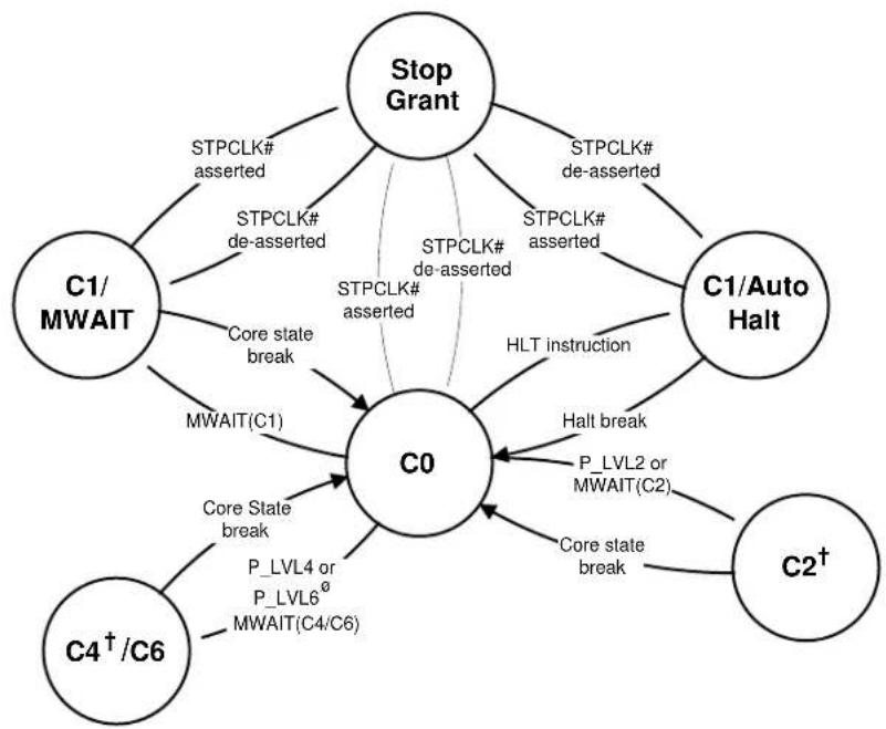
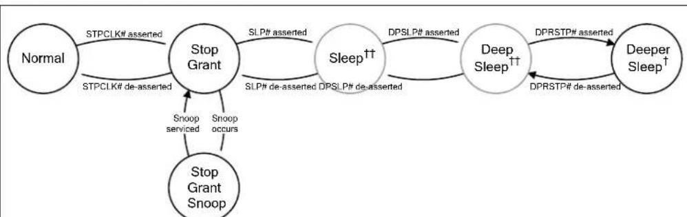
Figure 3-1 shows the thread low power states. Figure 3-2 shows the package low power states.
Note: STPCLK#, DPSLP#, and DPRSTP are internal signals only.
Figure 3-1. Thread Low Power States
flowchart
graph TD
    A["C1/MWAIT"] -->|STPCLK# asserted| B["Stop Grant"]
    A -->|STPCLK# de-asserted| B
    A -->|Core state break| C["C0"]
    C -->|HALT instruction| D["C1/Auto Halt"]
    C -->|Core State break| E["C4†/C6"]
    C -->|P_LVL4 or P_LVL6° MWAIT(C4/C6)| F["C2†"]
    B -->|STPCLK# de-asserted| B
    B -->|STPCLK# asserted| B
    C -->|Halt break| G["P_LVL2 or MWAIT(C2)"]
    C -->|Core state break| H["Core state break"]
halt break = A20M# transition, INIT#, INTR, NMI, PREQ#, RESET#, SMI#, or APIC interrupt core state break = (halt break OR Monitor event) AND STPCLK# high (not asserted) † — STPCLK# assertion and de-assertion have no effect if a core is in C2 or C4. ∅ — P_LVL6 read is issued once the L2 cache is reduced to zero.
Figure 3-2. Package Low Power States
flowchart
graph TD
    A["Normal"] -->|STPCLK# asserted| B["Stop Grant"]
    B -->|SLP# asserted| C["Sleep††"]
    C -->|DPSLP# asserted| D["Deep Sleep††"]
    D -->|DPRSTP# asserted| E["Deeper Sleep†"]
    E -->|DPRSTP# de-asserted| D
    D -->|DPSLP# de-asserted| C
    C -->|Snoop served| F["Stop Grant Snoop"]
    F -->|Snoop occurs| B
† – Deeper Sleep includes the C4 and C6 states †† – Sleep and Deep Sleep are not states directly supported by the processor, but rather sub-states of Silverthorne's C4/C6
3.1.1 Cx State Definitions
• C0 State—Full On
This is the only state that runs software. All clocks are running and the processor core is active. The processor can service snoops and maintain cache coherency in this state. All power management for interfaces, clock gating, are controlled at the unit level.
• C1 State—Auto-Halt
The first level of power reduction occurs when the core processor executes an Auto-Halt instruction. This stops the execution of the instruction stream and greatly reduces the core processor's power consumption. The core processor can service snoops and maintain cache coherency in this state. The Processor North Complex logic does not distinguish C1 from C0 explicitly.
• C2 State—Stop Grant
The next level of power reduction occurs when the core processor is placed into the Stop Grant state. The core processor can service snoops and maintain cache coherency in this state. The North Complex only supports receiving a single Stop Grant.
Entry into the C2 state will occur after the core processor requests C2 (or deeper). C2 state will be exited, entering the C0 state, when a break event is detected. Processor must ensure that the DLLs are awake and the memory will be out of self-refresh at this point.
• C1E and C2E States
C1E and C2E states are transparent to the north complex logic. The C1E state is the same as the C1 state, in that the core processor emits a HALT cycle when entering the state. There are no other visible actions from the core processor.
The C2E state is the same as the C2 state, in that the core processor emits a Stop Grant cycle when entering the state. There are no other visible actions from the core processor.
• C4 State—Deeper Sleep
In this state, the core processor shuts down its PLL and cannot handle snoop requests. The core processor voltage regulator is also told to reduce the processor's voltage. During the C4 state, the North Complex will continue to handle traffic to memory so long as this traffic does not require a snoop (i.e., no coherent traffic requests are serviced).
The C4 state is entered by receiving a C4 request from the core processor/OS. The exit from C4 occurs when the North Complex detects a snoopable event or a break event, which would cause it to wake up the core processor and initiate the C0 sequence.
• C4E
The C4E state is essentially the same as the C4 state except that the core processor will transition to the Low Frequency Mode (LFM) frequency and voltage upon entry and exit of this state.
• C6—Deep Power Down
Prior to entering the C6 state, the core processor will flush its cache and save its core context to a special on-die SRAM on a different power plane. Once the C6 entry sequence has completed, the core processor's voltage can be completely shut off.
The key difference for the North Complex logic between the C4 state and the C6 state is that since the core processor's cache is empty, there is no need to perform snoops on the internal FSB. This means that bus master events (which would cause a popup from the C4 state to the C2 state) can be allowed to flow unimpeded during the C6 state. However, the core processor must still be returned to the C0 state to service interrupts.
A residency counter is read by the core processor to enable an intelligent promotion/demotion based on energy awareness of transitions and history of residencies/transitions.
4 Electrical Specifications
This chapter contains signal group descriptions, absolute maximum ratings, voltage identification and power sequencing. This chapter also includes DC specifications.
4.1 Power and Ground Balls
The processor has Vcc and Vss (ground) inputs for on-chip power distribution. All power balls must be connected to their respective processor power planes, while all Vss balls must be connected to the system ground plane. Use of multiple power and ground planes is recommended to reduce I*R drop. The Vcc balls must be supplied with the voltage determined by the processor Voltage Identification (VID) signals.
4.2 Decoupling Guidelines
Due to large number of transistors and high internal clock speeds, the processor is capable of generating large current swings between low and full power states. This may cause voltages on power planes to sag below their minimum values, if bulk decoupling is not adequate. Larger bulk storage ( C_BULK ), such as electrolytic capacitors, supply current during longer lasting changes in current demand (for example, coming out of an idle condition). Similarly, capacitors act as a storage well for current when entering an idle condition from a running condition. To keep voltages within specification, output decoupling must be properly designed.
Caution: Design the board to ensure that the voltage provided to the processor remains within the specification. Failure to do so can result in timing violations or reduced lifetime of the processor.
4.3 Voltage Rail Decoupling
The voltage regulator solution needs to provide:
• Bulk capacitance with low effective series resistance (ESR).
• A low path impedance from the regulator to the processor.
- Bulk decoupling to compensate for large current swings generated during power-on, or low-power idle state entry/exit.
The power delivery solution must ensure that the voltage and current specifications are met, as defined in Table 4-4.
4.4 Voltage Identification (VID)
The V_cc and V_NN voltage inputs use two encoding pins (VIDEN[1:0]) to enable the VID pin inputs and seven voltage identification pins (VID[6:0]) to select the power supply voltage. The VID/VIDEN pins for the processor are CMOS outputs driven by the processor VID circuitry. Table 4-2 specifies the voltage level corresponding to the state of VID[6:0]. A “1” in this refers to a high-voltage level and a “0” refers to a low-voltage level. For more details about PMIC design to support the processor power supply requirements, refer to the vendor's specification.
4.4.1 VID Enable
Both V_CC and V_NN are variable in Intel® Atom™ Processor Z670. Processor implements a new VID mechanism that minimizes the number of required pins. The VID for V_NN and V_CC are multiplexed on to the same set of pins and a separate 2-bit enable/ID is defined to specify what the driven VID corresponds to. One of the combinations is used to notify that the VID is invalid. This is used when the processor is in C6/Standby to tri-state the VID pins to save power.
Table 4-1. VIDEN Encoding
| VIDEN[1:0] Description | |
| 00b VID is invalid | |
| 01b VID for V | CC |
| 10b VID for V | NN |
| 11b Reserved |
4.4.2 VID Table
Note:
- Processor will not support the entire range of the voltages listed in the VID table (grayed out).
- VID codes below 0.3 V are not supported for V_cc .
Table 4-2. VID Table
| VID[6:0] V | cc/VNN | VID[6:0] V | cc/VNN | VID[6:0] V | cc/VNN | VID[6:0] V | cc/VNN |
| 00h | 1.5000V | 20h | 1.1000V | 40h | 0.7000V | 60h | 0.3000V |
| 01h | 1.4875V | 21h | 1.0875V | 41h | 0.6875V | 61h | 0.2875V |
| 02h | 1.4750V | 22h | 1.0750V | 42h | 0.6750V | 62h | 0.2750V |
| 03h | 1.4625V | 23h | 1.0625V | 43h | 0.6625V | 63h | 0.2625V |
| 04h | 1.4500V | 24h | 1.0500V | 44h | 0.6500V | 64h | 0.2500V |
| 05h | 1.4375V | 25h | 1.0375V | 45h | 0.6375V | 65h | 0.2375V |
| 06h | 1.4250V | 26h | 1.0250V | 46h | 0.6250V | 66h | 0.2250V |
| 07h | 1.4125V | 27h | 1.0125V | 47h | 0.6125V | 67h | 0.2125V |
| 08h | 1.4000V | 28h | 1.0000V | 48h | 0.6000V | 68h | 0.2000V |
| 09h | 1.3875V | 29h | 0.9875V | 49h | 0.5875V | 69h | 0.1875V |
| 0Ah | 1.3750V | 2Ah | 0.9750V | 4Ah | 0.5750V | 6Ah | 0.1750V |
| 0Bh | 1.3625V | 2Bh | 0.9625V | 4Bh | 0.5625V | 6Bh | 0.1625V |
| 0Ch | 1.3500V | 2Ch | 0.9500V | 4Ch | 0.5500V | 6Ch | 0.1500V |
| 0Dh | 1.3375V | 2Dh | 0.9375V | 4Dh | 0.5375V | 6Dh | 0.1375V |
| 0Eh | 1.3250V | 2Eh | 0.9250V | 4Eh | 0.5250V | 6Eh | 0.1250V |
| 0Fh | 1.3125V | 2Fh | 0.9125V | 4Fh | 0.5125V | 6Fh | 0.1125V |
| 10h | 1.3000V | 30h | 0.9000V | 50h | 0.5000V | 70h | 0.1000V |
| 11h | 1.2875V | 31h | 0.8875V | 51h | 0.4875V | 71h | 0.0875V |
| 12h | 1.2750V | 32h | 0.8750V | 52h | 0.4750V | 72h | 0.0750V |
| 13h | 1.2625V | 33h | 0.8625V | 53h | 0.4625V | 73h | 0.0625V |
| 14h | 1.2500V | 34h | 0.8500V | 54h | 0.4500V | 74h | 0.0500V |
| 15h | 1.2375V | 35h | 0.8375V | 55h | 0.4375V | 75h | 0.0375V |
| 16h | 1.2250V | 36h | 0.8250V | 56h | 0.4250V | 76h | 0.0250V |
| 17h | 1.2125V | 37h | 0.8125V | 57h | 0.4125V | 77h | 0.0125V |
| 18h | 1.2000V | 38h | 0.8000V | 58h | 0.4000V | 78h | 0.0000V |
| 19h | 1.1875V | 39h | 0.7875V | 59h | 0.3875V | 79h | 0.0000V |
| 1Ah | 1.1750V | 3Ah | 0.7750V | 5Ah | 0.3750V | 7Ah | 0.0000V |
| 1Bh | 1.1625V | 3Bh | 0.7625V | 5Bh | 0.3625V | 7Bh | 0.0000V |
| VID[6:0] V _CC / V_NN | VID[6:0] V | _CC / V_NN | VID[6:0] V | _CC / V_NN | VID[6:0] V | _CC / V_NN |
| 1Ch | 1.1500V | 3Ch | 0.7500V | 5Ch | 0.3500V | 7Ch |
| 1Dh | 1.1375V | 3Dh | 0.7375V | 5Dh | 0.3375V | 7Dh |
| 1Eh | 1.1250V | 3Eh | 0.7250V | 5Eh | 0.3250V | 7Eh |
| 1Fh | 1.1125V | 3Fh | 0.7125V | 5Fh | 0.3125V | 7Fh |
4.5 Absolute Maximum Ratings
Table 4-3 specifies absolute maximum and minimum ratings. Within functional operation limits, functionality and long-term reliability can be expected.
At conditions outside functional operation condition limits, but within absolute maximum and minimum ratings, neither functionality nor long term reliability can be expected. If a device is returned to conditions within functional operation limits after having been subjected to conditions outside these limits, but within the absolute maximum and minimum ratings, the device may be functional, but with its lifetime degraded depending on exposure to conditions exceeding the functional operation condition limits.
At conditions exceeding absolute maximum and minimum ratings, neither functionality nor long term reliability can be expected. Moreover, if a device is subjected to these conditions for any length of time, then when returned to conditions within the functional operating condition limits, it will either not function or its reliability will be severely degraded.
Although the processor contains protective circuitry to resist damage from static electric discharge, precautions should always be taken to avoid high static voltages or electric fields.
Table 4-3. Absolute Maximum Ratings
| Symbol | Parameter | Minimum | Maximum | Unit | Note |
| V_CC | Processor core supply voltage | -0.3 | 1.1 | V | |
| V_NN | North Complex logic and GFX supply voltage | -0.3 | 0.95 | V | |
| V_CCR/V_CCQ | cDMI, cDVO, LGI, LGIe | -0.3 | 1.1 | V | |
| V_CCPDDR | 1.05-V DDR2 DLL and logic supply voltage | -0.3 | 1.1 | V | |
| V_CCPAOAC | 1.05-V JTAG, C6 SRAM | -0.3 | 1.1 | V | |
| V_MM | 1.2-V I/O supply voltage | -0.3 | 1.25 | V | |
| LVD_VBG | 1.25-V LVDS band gap supply voltage | -0.1 | 1.28 | V | |
| V_CCA | 1.5-V HPLL analog PLL and thermal sensor supply voltage | -0.3 | 1.575 | V | |
| V_CCA180 | 1.8-V LVDS analog supply voltage | -0.3 | 1.9 | V | |
| V_CCD180 | 1.8-V LVDS I/O supply voltage | -0.3 | 1.9 | V | |
| V_CC180SR | 1.8-V DDR2 self-refresh supply voltage | -0.4 1.9 | V | ||
| V_CC180 | 1.8-V DDR2 I/O supply voltage | -0.4 | 1.9 | V | |
| T_J | Operational junction temperature | 0 | 90 | °C | 1,2 |
| T_SUSTAINED STORAGE | The ambient storage temperature limit (in shipping media) for a sustained period of time. | -5 °C | 40 °C | °C | 4 |
| RH_SUSTAINED STORAGE | The maximum device storage relative humidity for a sustained period of time. | 60% @ 24 °C | 4,5 | ||
| TIME_SUSTAINE D STORAGE | A prolonged or extended period of time; typically associated with customer shelf life. | 0 | 6 | Months | 5 |
NOTE:
- As measured by the activation of the on-die Intel® Thermal Monitor. The Intel Thermal Monitor's automatic mode is used to indicate that the maximum T_J has been reached. Refer to Section 5.2 for more details.
- The Intel Thermal Monitor automatic mode must be enabled for the processor to operate within specifications.
- The storage temperature is applicable to storage conditions only. Storage within these limits will not affect the long-term reliability of the device. For functional operation, refer to the processor case temperature specifications.
- The JEDEC, J-JSTD-020 moisture level rating and associated handling practices apply to all moisture sensitive devices removed from the moisture barrier bag.
- Nominal temperature and humidity conditions and durations are given and tested within the constraints imposed by T_SUSTAINED and customer shelf life in applicable Intel box and bags.
4.6 DC Specifications
Table 4-4. Voltage and Current Specifications
| Symbol | Parameter | Min. | Typ. | Max. | Unit | Notes ^1,2 | |
| V_CCHFM | V_CC @ Highest Frequency Mode | AVID | - | 1.15 | V | 3 | |
| V_CCLFM | V_CC @ Lowest Frequency Mode | 0.7 | - | AVID | V | 3 | |
| V_CCBOOT | Default V_CC for initial power on | V_CCLFM | V | 4 | |||
| V_NNBOOT | V_NN | V | 4 | ||||
| V_NN | V_NN supply voltage | 0.75 | 0.95 | V | 3 | ||
| V_CCP | V_CCP supply voltage | 0.9975 | 1.05 | 1.1025 | V | 4 | |
| V_CCQ | V_CCQ supply voltage | 0.9975 | 1.05 | 1.1025 | V | ||
| V_CCPDDR | V_CCPDDR supply voltage | 1.029 | 1.05 | 1.071 | V | 5 | |
| Symbol | Parameter | Min. | Typ. | Max. | Unit | Notes1,2 | |
| V_CCPAOAC | V_CCPAOAC supply voltage | 0.9975 | 1.05 | 1.1025 | V | ||
| V_MM | V_MM supply voltage | 1.14 | 1.20 | 1.26 | V | ||
| LVD_VBG | LVDS band gap reference voltage | 1.225 | 1.25 | 1.275 | V | ||
| V_CCA | V_CCA supply voltage | 1.47 | 1.5 | 1.53 | V | ||
| V_CCA180 | V_CCA180 supply voltage | 1.746 | 1.8 | 1.854 | V | ||
| V_CCD180 | V_CCD180 supply voltage | 1.71 | 1.8 | 1.89 | V | ||
| V_CC180SR | V_CC180SR supply voltage | 1.71 | 1.8 | 1.89 | V | ||
| V_CC180 | V_CC180 supply voltage | 1.71 | 1.8 | 1.89 | V | ||
| I_VCC | Processor Number | Core Frequency | - | - | - | - | |
| Z670 | HFM: 1.5 GHzLFM: 0.6 GHz | - | - | 2.50 | A | 6,7 | |
| I_VNN | V_NN supply current | - | - | 1.60 | A | 7 | |
| I_VCCP | V_CCP supply current | - | - | 0.121 | A | 7 | |
| I_VCCQ | V_CCQ supply current | - | - | 0.015 | A | 7 | |
| I_VCCPDDR | V_CCPDDR supply current | - | - | 0.150 | A | 7 | |
| I_VCCPAOAC | V_CCPAOAC supply current | - | - | 0.030 | A | 7 | |
| I_VMM | V_MM supply current | - | - | 0.010 | A | 7 | |
| I_VCCA | V_CCA supply current | - | - | 0.150 | A | 7 | |
| I_VCCA180 | V_CCA180 supply current | - | - | 0.050 | A | 7,8,9 | |
| I_VCCD180 | V_CCD180 supply current | - | - | A | |||
| I_VCC180SR | V_CC180SR supply current | - | - | 0.010 | A | 7 | |
| I_VCC180 | V_CC180 supply current | - | - | 0.400 | A | 7 | |
NOTES:
- Maximum specifications are based on measurements done with currently existing workloads and test conditions. These numbers are subject to change.
- Specified at T_J = 90^ .
- Each processor is programmed with a maximum valid voltage identification value (VID), which is set at manufacturing and cannot be altered. Individual maximum VID values are calibrated during manufacturing such that two processors at the same frequency may have different settings within the VID range. Note that this differs from the VID employed by the processor during a power management event (Thermal Monitor 2, Enhanced Intel SpeedStep® Technology, or Enhanced Halt State). Typical AVID range is 0.70V to 1.15V for V_CC and 0.75V to 0.95V for V_NN .
- This specification corresponds to what value gets driven by the processor. It is possible for firmware to override these values.
- Voltage specification of ±2% includes AC and DC variations. The sum of AC noise and DC variations should not exceed 1.05V ±2%.
- Specified at the nominal V_cc .
-
Peak Sustained Current is defined as the maximum sustainable current measured as an RMS value over 1 s.
-
This is the sum of current on both rails.
- Specification based on LVDS panel configuration of 1024x600 resolution, 60Hz refresh rate, and 18bpp color depth.
Table 4-5. Differential Clock DC Specifications
| Symbol | Parameter | Min. | Typ. | Max. | Unit | Notes |
| Differential Clock (BCLK) | ||||||
| V_IH | Input high voltage | - | - | 1.15 | V | |
| V_IL | Input low voltage | - | - | -0.3 | V | |
| V_CROSS | Crossing voltage | 0.3 | - | 0.55 | V | |
| V_CROSS | Range of crossing points | - | - | 140 | mV | |
| V_SWING | Differential output swing | 300 | - | - | mV | |
| I_LI | Input leakage current | -5 | - | +5 | μA | |
| C_PAD | Pad capacitance | 1.2 | 1.45 | 2.0 | pF | |
Table 4-6. AGTL+, CMOS, and CMOS Open Drain Signal Group DC Specifications
| Symbol | Parameter | Min. | Typ. | Max. | Unit | Notes |
| GTLREF | GTL reference voltage | - | 2/3 V_CCP | - | V | |
| CMREF | CMOS reference voltage | - | 1/2 V_CCP | - | V | |
| R_COMP | Compensation resistor | 27.73 | 27.5 | 27.78 | Ω | 10 |
| R_ODT | Termination resistor | - | 55 | - | Ω | 11 |
| V_IH (GTL) | Input high voltage GTL signal | GTLREF+ 0.10 | V_CCP | V_CCP + 0.10 | V | 3, 6 |
| V_IL (GTL) | Input low voltage GTL signal | -0.10 | 0 | GTLREF- 0.10 | V | 2, 4 |
| V_IH (CMOS) | Input high voltage CMOS signal | CMREF+ 0.10 | V_CCP | V_CCP + 0.10 | V | 3, 6 |
| V_IL (CMOS) | Input low voltage CMOS signal | -0.10 | 0 | CMREF- 0.10 | V | 2, 4 |
| V_OH Output high voltage V | _CCP - 0.10 | V_CCP | V_CCP | V | 6 | |
| R_TT (GTL) | Termination resistance | 46 | 55 | 61 | Ω | 7 |
| R_TT (CMOS) | Termination resistance | 46 | 55 | 61 | Ω | 11 |
| R_ON (GTL) | GTL buffer on resistance | 21 | 25 | 29 | Ω | 5 |
| R_ON (CMOS) | CMOS buffer on resistance | 42 | 50 | 55 | Ω | 12 |
| R_ON (CMOS_C) | CMOS common clock buffer on resistance | 42 | 50 | 58 | Ω | 12 |
| I_LI | Input leakage current | - | - | ±100 | μA | 8 |
| C_PAD | Pad capacitance | 1.6 | 2.1 | 2.55 | pF | 9 |
NOTES:
- Unless otherwise noted, all specifications in this table apply to all processor frequencies.
- VIL is defined as the maximum voltage level at a receiving agent that will be interpreted as a logical low value.
- VIH is defined as the minimum voltage level at a receiving agent that will be interpreted as a logical high value.
- VIH and VOH may experience excursions above VCCP. However, input signal drivers must comply with the signal quality specifications.
- RON is the pull-down driver resistance. Refer to processor I/O Buffer Models for I/V characteristics. Measured at 0.33* VCCP.
- GTLREF and CMREF should be generated from VCCP with a 1% tolerance resistor divider. The VCCP referred to in these specifications is the instantaneous VCCP.
- RTT is the on-die termination resistance measured at VOL of the AGTL+ output driver. Measured at 0.33* VCCP. RTT is connected to VCCP on die. Refer to processor I/O buffer models for I/V characteristics.
- Specified with on die RTT and RON are turned off. VIN between 0 and VCCP.
- CPAD includes die capacitance only. No package parasitics are included.
- This is the external resistor on the component pins.
- On die termination resistance for CMOS is measured at 0.5* VCCP.
- RON for CMOS pull-down driver resistance. Refer to processor I/O Buffer Models for I/V characteristics. Measured at 0.5^*V_CCP .
Table 4-7. CMOS1.8 Signal Group DC Specifications
| Symbol | Parameter | Min. | Typ. | Max. | Unit | Notes |
| V_IH Input | high voltage (V | _CC180/2)+ 0.125 | - 1.9 V | |||
| V_IL | Input low voltage | -0.4 | - | (V_CC180/2)- 0.125 | V | |
| V_OH | Output high voltage | (V_CC180/2)+ 0.25 | - | - | V | |
| V_OL | Output low voltage | - | - | (V_CC180/2)- 0.25 | V |
NOTES:
- Unless otherwise noted, all specifications in this table apply to all processor frequencies.
- V _IL is defined as the maximum voltage level at a receiving agent that will be interpreted as a logical low value.
- V_IH is defined as the minimum voltage level at a receiving agent that will be interpreted as a logical high value.
- V_IH and V_OH may experience excursions above V_CCP . However, input signal drivers must comply with the signal quality specifications.
Table 4-8. LVDS Signal Group DC Specifications
| Symbol | Parameter | Min. | Typ. | Max. | Unit | Notes |
| V_OS | Offset voltage | 1.125 | 1.25 | 1.375 | V | |
| V_OS | Change in offset voltage | - | - | 50 | mV | |
| V_OD | Differential output voltage | 250 | 350 | 450 | mV | |
| V_OD Change | in differential output voltage | - | - | 50 | mV | |
| I_SC | Short-circuit current | - | - | 12 | mA | |
| I_SCC | Short-circuit comment current | - | - | 24 | mA | |
| I_L | Leakage current | -380 | 150 | 380 | μA | |
| Dynamic offset | - | - | 150 | mV | ||
| Overshoot | 50 | 70 | 90 | mV | ||
| Ringback | 50 | 70 | 90 | mV |
NOTE: Unless otherwise noted, all specifications in this table apply to all processor frequencies.
5 Thermal Specifications and Design Considerations
The processor requires a thermal solution to maintain temperatures within operating limits as set forth in Table 4-3. Any attempt to operate the processor outside these operating limits may result in permanent damage to the processor and potentially other components in the system. Maintaining the proper thermal environment is the key to reliable, long-term system operation. A complete thermal solution includes both component and system level thermal management features.
Note: Trading thermal solutions also involves trading performance.
To allow for the optimal operation and long-term reliability of Intel processor-based systems, the system/processor thermal solution should be designed such that the processor remains within the minimum and maximum junction temperature ( T_j ) specifications at the corresponding Thermal Design Power (TDP) value listed in Table 5-1. Thermal solutions not designed to provide this level of thermal capability may affect the long-term reliability of the processor and system.
The maximum junction temperature is defined by an activation of the processor Intel® Thermal Monitor. Refer to Section 5.2 for more details. Analysis indicates that real applications are unlikely to cause the processor to consume the theoretical maximum power dissipation for sustained time periods. Intel recommends that complete thermal solution designs target the TDP indicated in Table 5-1. The Intel® Thermal Monitor feature is designed to help protect the processor in the unlikely event that an application exceeds the TDP recommendation for a sustained period of time. For more details on the usage of this feature, refer to Section 5.2. In all cases, the Intel® Thermal Monitor feature must be enabled for the processor to remain within specification.
Table 5-1. Thermal Design Power Specifications
| Symbol | Processor Number | Core Frequency | Thermal Design Power | Unit Notes | |||
| TDP Z670 | 1.5 GHz and HFM VCC0.6 GHZ and LFM VCC | 3.0 | W 1,2 | ||||
| Symbol | Parameter | Min | Typ | Max | Unit | Notes | |
| Tj Junction Temperature | 0 | -90 | °C | ||||
| HD Streaming Scenario Power | - | 1.02 | - | W 3,4 | |||
NOTES:
- The TDP specification should be used to design the processor thermal solution. The TDP is not the maximum theoretical power the processor can generate.
-
The Intel Thermal Monitor automatic mode must be enabled for the processor to operate within specifications.
-
Scenario Power examines a common use case and may be more indicative of a more common power usage level as compared with the TDP. Measurement configuration assumes: LCD brightness 100nits, LCD 1024x800 10.1", USB touch panel, I ^2 C sensors, SDIO WiFi on, 2GB DDR2, 73% PMIC efficiency, 93% discrete VR efficiency, Flash* v10.2.
- 720p, YouTube*.
5.1 Temperature Monitoring
The processor incorporates two methods of monitoring die temperature:
• By Intel Thermal Monitor
• By Digital Thermal Sensor (DTS)
The Intel Thermal Monitor (detailed in Section 5.2) must be used to determine when the maximum specified processor junction temperature has been reached.
5.2 Intel ^® Thermal Monitor
The Intel Thermal Monitor helps control the processor temperature by activating the TCC (Thermal Control Circuit) when the processor silicon reaches its maximum operating temperature. The temperature at which the Intel® Thermal Monitor activates the TCC is not user configurable. Bus traffic is snooped in the normal manner and interrupt requests are latched (and serviced during the time that the clocks are on) while the TCC is active.
With a properly designed and characterized thermal solution, it is anticipated that the TCC would only be activated for very short periods of time when running the most power intensive applications. The processor performance impact due to these brief periods of TCC activation is expected to be minor and hence not detectable.
An under- designed thermal solution that is not able to prevent excessive activation of the TCC in the anticipated ambient environment may cause a noticeable performance loss and may affect the long-term reliability of the processor. In addition, a thermal solution that is significantly under-designed may not be capable of cooling the processor even when the TCC is active continuously.
The Intel Thermal Monitor controls the processor temperature by modulating (starting and stopping) the processor core clocks or by initiating an Enhanced Intel SpeedStep® Technology transition when the processor silicon reaches its maximum operating temperature. The Intel Thermal Monitor uses two modes to activate the TCC: automatic mode and on-demand mode. If both modes are activated, automatic mode takes precedence.
There are two automatic modes called the Intel Thermal Monitor 1 (TM1) and the Intel Thermal Monitor 2 (TM2). These modes are selected by writing values to the MSRs of the processor. After the automatic mode is enabled, the TCC will activate only when the internal die temperature reaches the maximum allowed value for operation.
The Intel® Thermal Monitor automatic mode must be enabled through IA-32 Firmware for the processor to be operating within specifications. Intel recommends that the TM1 mode and the TM2 mode be enabled on the processor.
When the TM1 mode is enabled and a high temperature situation exists, the clocks will be modulated by alternately turning the clocks off and on at a 50 percent duty cycle. Cycle times are processor speed dependent and will decrease linearly as processor core frequencies increase. Once the temperature has returned to a non-critical level, modulation ceases and TCC goes inactive. A small amount of hysteresis has been included to prevent rapid active/inactive transitions of the TCC when the processor temperature is near the trip point. The duty cycle is factory configured and cannot be modified. Also, automatic mode does not require any additional hardware, software drivers, or interrupt handling routines. Processor performance will be decreased by the same amount as the duty cycle when the TCC is active.
When the TM2 mode is enabled and a high temperature situation exists, the processor will perform an Enhanced Intel SpeedStep Technology transition to the LFM. When the processor temperature drops below the critical level, the processor will make an Enhanced Intel SpeedStep Technology transition to the last requested operating point.
The Intel Thermal Monitor automatic mode and Enhanced Intel SpeedStep Technology must be enabled through IA-32 Firmware for the processor to be operating within specifications. Intel recommends that TM1 and TM2 be enabled on the processors.
TM1 and TM2 can co-exist within the processor. If both TM1 and TM2 bits are enabled in the auto-throttle MSR, TM2 will take precedence over TM1. However, if Force TM1 over TM2 is enabled in MSRs using IA-32 Firmware and TM2 is not sufficient to cool the processor below the maximum operating temperature, then TM1 will also activate to help cool down the processor.
If a processor load-based Enhanced Intel SpeedStep Technology transition (through MSR write) is initiated when a TM2 period is active, there are two possible results:
- If the processor load-based Enhanced Intel SpeedStep Technology transition target frequency is higher than the TM2 transition based target frequency, the processor load-based transition will be deferred until the TM2 event has been completed.
- If the processor load-based Enhanced Intel SpeedStep Technology transition target frequency is lower than the TM2 transition based target frequency, the processor will transition to the processor load-based Enhanced Intel® SpeedStep® Technology target frequency point.
The TCC may also be activated using on-demand mode. If bit 4 of the ACPI Intel® Thermal Monitor control register is written to a 1, the TCC will be activated immediately independent of the processor temperature. When using on-demand mode to activate the TCC, the duty cycle of the clock modulation is programmable using bits 3:1 of the same ACPI Intel Thermal Monitor control register. In automatic mode, the duty cycle is fixed at 50% on, 50% off. However in on-demand mode, the duty cycle can be programmed from 12.5% on/87.5% off, to 87.5% on/12.5% off in 12.5% increments.
On-demand mode may be used at the same time automatic mode is enabled; however, if the system tries to enable the TCC using on-demand mode at the same time automatic mode is enabled and a high temperature condition exists, automatic mode will take precedence.
An external signal, PROCHOT# (processor hot) is asserted when the processor detects that its temperature is above the thermal trip point. Bus snooping and interrupt latching are also active while the TCC is active.
Besides the thermal sensor and thermal control circuit, the Intel Thermal Monitor also includes one ACPI register, one performance counter register, three MSRs, and one I/O pin (PROCHOT#). All are available to monitor and control the state of the Intel® Thermal Monitor feature. The Intel® Thermal Monitor can be configured to generate an interrupt upon the assertion or de-assertion of PROCHOT#.
PROCHOT# will not be asserted when the processor is in the Sleep, Deep Sleep, and Deeper Sleep low power states (see Figure 3-2). If the platform thermal solution is not able to maintain the processor junction temperature within the maximum specification, the system must initiate an orderly shutdown to prevent damage. If the processor enters one of the above low power states with PROCHOT# already asserted, then PROCHOT# will remain asserted until the processor exits the low power state and the processor junction temperature drops below the thermal trip point.
If the Intel Thermal Monitor automatic mode is disabled, the processor will operate out of specification. Regardless of enabling the automatic or on-demand modes, in the event of a catastrophic cooling failure, the processor will automatically shut down when the silicon has reached a potentially catastrophic temperature. At this point the THERMTRIP# signal will go active. THERMTRIP# activation is independent of processor activity and does not generate any bus cycles.
Table 5-2. Support for PROCHOT# / THERMTRIP# in Active and Idle States
| System State | Core State | PROCHOT# (Bidirectional) | THERMTRIP# | ||||
| Input Output | |||||||
| Core | North Complex | Core | North Complex | Core | North Complex | ||
| S0 | C0 | Supported | Optional | Active | Active | Active | Active |
| C1/C1E | Supported | Optional | Active | Active | Active | Active | |
| C2/C2E | Supported | Optional | Active | Active | Active | Active | |
| C4/C4E | Ignored | Optional | Inactive | Active | Not Guaranteed | Active | |
| C6 | Ignored | Optional | Inactive | Active | Inactive | Active | |
5.2.1 Digital Thermal Sensor
The processor also contains an on die Digital Thermal Sensor (DTS) that is read using an MSR (no I/O interface). The processor has a unique digital thermal sensor that's temperature is accessible using the processor MSRs. The DTS is the preferred method of reading the processor die temperature since it can be located much closer to the hottest portions of the die and can thus more accurately track the die temperature and potential activation of processor core clock modulation using the Thermal Monitor. The DTS is only valid while the processor is in the normal operating state (the Normal package level low power state).
Unlike traditional thermal devices, the DTS outputs a temperature relative to the maximum supported operating temperature of the processor ( T_J_max ). It is the responsibility of software to convert the relative temperature to an absolute temperature. The temperature returned by the DTS will always be at or below T_J_max .
Catastrophic temperature conditions are detectable using an Out of Specification status bit. This bit is also part of the DTS MSR. When this bit is set, the processor is operating out of specification and immediate shutdown of the system should occur. The processor operation and code execution is not ensured once the activation of the Out of Specification status bit is set.
The DTS-relative temperature readout corresponds to the Intel® Thermal Monitor (TM1/TM2) trigger point. When the DTS indicates maximum processor core temperature has been reached, the TM1 or TM2 hardware thermal control mechanism will activate. The system designer is required to use the DTS to ensure proper operation of the processor within its temperature operating specifications.
Changes to the temperature can be detected using two programmable thresholds located in the processor MSRs. These thresholds have the capability of generating interrupts using the core's local APIC. Refer to the Intel ^® 64 and IA-32 Architectures Software Developer's Manuals for specific register and programming details.
5.2.2 Out of Specification Detection
Overheat detection is performed by monitoring the processor temperature and temperature gradient. This feature is intended for graceful shut down before the THERMTRIP# is activated. If the processor's TM1 or TM2 are triggered and the temperature remains high, an "Out Of Specification" status and sticky bit are latched in the status MSR register and generates thermal interrupt.
5.2.3 Catastrophic Thermal Protection
The processor supports the THERMTRIP# signal for catastrophic thermal protection. An external thermal sensor should also be used to protect the processor and the system against excessive temperatures. Even with the activation of THERMTRIP#, which halts all processor internal clocks and activity, leakage current can be high enough such that the processor cannot be protected in all conditions without the removal of power to the processor. If the external thermal sensor detects a potentially catastrophic processor temperature, or if the THERMTRIP# signal is asserted by the processor, the V_cc supply to the processor must be turned off within 500 ms to prevent permanent silicon damage due to thermal runaway of the processor. THERMTRIP# functionality is not ensured if the PWRGOOD signal is not asserted.
5.2.4 PROCHOT# Signal Pin
An external signal, PROCHOT# (processor hot), is asserted when the processor die temperature has reached its maximum operating temperature. If TM1 or TM2 is enabled, then the TCC will be active when PROCHOT# is asserted. The processor can be configured to generate an interrupt upon the assertion or deassertion of
PROCHOT#. Refer to the Intel ^® 64 and IA-32 Architectures Software Developer's Manuals.
The processor implements a bi-directional PROCHOT# capability to allow system designs to protect various components from overheating situations. The PROCHOT# signal is bi-directional in that it can either signal when the processor has reached its maximum operating temperature or be driven from an external source to activate the TCC. The ability to activate the TCC using PROCHOT# can provide a means for thermal protection of system components.
Only a single PROCHOT# pin exists at a package level of the processor. When the core's thermal sensor trips, the PROCHOT# signal is driven by the processor package. If only TM1 is enabled, PROCHOT# will be asserted and only the core that is above TCC temperature trip point will have its core clocks modulated. If TM2 is enabled and the core is above TCC temperature trip point, it will enter the lowest programmed TM2 performance state. It is important to note that Intel recommends that both TM1 and TM2 be enabled.
When PROCHOT# is driven by an external agent, if only TM1 is enabled on the core, then the processor core will have the clocks modulated. If TM2 is enabled, then the processor core will enter the lowest programmed TM2 performance state. It should be noted that Force TM1 on TM2, enabled using IA-32 Firmware, does not have any effect on external PROCHOT#. If PROCHOT# is driven by an external agent when TM1, TM2, and Force TM1 on TM2 are all enabled, then the processor will still apply only TM2.
PROCHOT# may be used for thermal protection of voltage regulators (VR). System designers can create a circuit to monitor the VR temperature and activate the TCC when the temperature limit of the VR is reached. By asserting PROCHOT# (pulled-low) and activating the TCC, the VR will cool down as a result of reduced processor power consumption.
Bi-directional PROCHOT# can allow VR thermal designs to target maximum sustained current instead of maximum current. Systems should still provide proper cooling for the VR and rely on bi-directional PROCHOT# only as a backup in case of system cooling failure. The system thermal design should allow the power delivery circuitry to operate within its temperature specification even while the processor is operating at its TDP.
With a properly designed and characterized thermal solution, it is anticipated that bi-directional PROCHOT# would only be asserted for very short periods of time when running the most power-intensive applications. An under-designed thermal solution that is not able to prevent excessive assertion of PROCHOT# in the anticipated ambient environment may cause a noticeable performance loss.
6 Package Mechanical Specifications and Pin Information
This chapter describes the package specifications and pinout assignments.
6.1 Package Mechanical Specifications
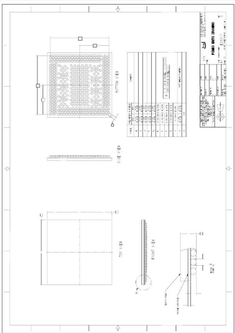
The processor will be available in a 518 pin FCMB3 package. The package dimensions are shown in Figure 6-1.
Figure 6-1. Package Mechanical Drawing
6.2 Processor Pinout Assignment
Table 6-1, Table 6-2 and Table 6-3 are graphic representations of the processor pinout assignments. Table 6-4 lists the pinout by signal name.
Table 6-1. Processor Pinout (Top View—Columns 21–31)
| 31 | 30 | 29 | 28 | 27 | 26 | 25 | 24 | 23 | 22 | 21 | |
| AL | Vss | Vss CDV | O_TX3 CDVC | TX2 | CDVO_TXST B_ODD# | CDVO_CVREF | CDMI_RXCHAR# | CDMI_RXSTB_EVEN# | CDMI_RX6 AL | ||
| AK | CDVO_TXDP WR# | CDVO | TX4 CDVO | TX0 | CDVO_TXST B_EVEN# | CDVO_RCOMP0 | CDVO_VBLANK# | CDMI_RXSTB_ODD# | AK | ||
| AJ | LA_DATAP0 | LA_DATAN0 | Vss | LA_DATAP1 | Vss | Vss | Vss | Vss | Vss AJ | ||
| AH | LA_CLKP | Vss | CDVO_STALL# | CDVO_TX5 | CDVO_TX1 | CDVO_RCOMP1 | VccQ 2 AH | ||||
| AG | LA_CLKN | LA_DATAN1 | Vss | Vss | AG | ||||||
| AF | LA_DATAN2 | LA_DATAP2 | Vss | LA_DATAN3 | VCCD180 | VCCA180 | V | CCP AF | |||
| AE | LA_IBG | Vss | Vss | Vss | Vss AE | ||||||
| AD | RSVD | LA_VBG | Vss | LA_DATAP3 | VCCD180 | VCCA180 | V | CCP AD | |||
| AC | RSVD | VCCP | Vss | Vss | Vss AC | ||||||
| AB | TP3 | Vss | |||||||||
| AA | TP5 | TP4 | Vss | VCCPADAC | VNN | RSVD9 | Vcc | AA | |||
| Y | TP6 | RSVD8 | VNN | Vss | Vss | ||||||
| W | TP2 | TP1 | Vss | THRMDA | VNN | Vcc | Vcc | ||||
| V | TP7 | Vss | VNN | Vss | Vss | ||||||
| U | TP8 | THRMDC | VNN | Vcc | Vcc | ||||||
| T | TP9 | TP10 | VNNSENSE | Vss | VNN | Vss | Vss | ||||
| R | VNN | VNN | VNN | VNN | VNN | ||||||
| P | Vss | VNN | Vss | VNN | VNN | Vss | Vss | ||||
| N | V | NN | VNN | VNN | VNN | VNN | |||||
| M | VNN | Vcc180 | VNN | Vcc180 | V | NN | Vss | Vss | |||
| L | Vcc180 | Vcc180 | V | NN | |||||||
| K | V | cc180 | V | cc180 | V | ss | Vss | ||||
| J | SM_DQ1 | SM_DQ0 | Vss | SM_BS2 | |||||||
| H | SM_DQ3 | Vss | V | cc180 V | cc180 | V | CCPDDR | ||||
| G | SM_DQS1 | SM_DQ2 | Vss | SM_BS1 | Vss | Vss | Vss | ||||
| F | SM_DM0 | SM_MA2 | Vcc180 V | cc180 | V | CCPDDR | |||||
| E | SM_DQ5 | Vss | Vss | Vss | |||||||
| D | SSM_DQ4 | SM_MA4 | SM_MA12 | SM_BS0 | SM_MA3 | SM_MA7 | SM_MA8 | SM_MA0 | |||
| C | SM_DQ6 V | ss | VSS | Vss | Vss | Vss | Vss | Vss | |||
| B | SM_DQ7 | SM_DQ8 | SM_DQ10 | SM_DQS0 | SM_DQ12 | SM_DQ14 | SM_RCVENO UT | SM_RCVENI N | |||
| A | Vss | SM_DQ9 | SM_DQ11 | SM_DM1 | SM_MA10 | SM_DQ13 | SM_DQ15 | SM_MA1 | |||
| 31 | 30 | 29 | 28 | 27 | 26 | 25 | 24 | 23 | 22 | 21 |
Table 6-2. Processor Pinout (Top View—Columns 11–20)
| 20 | 19 | 18 | 17 | 16 | 15 | 14 | 13 | 12 | 11 | |
| AL | CDMI_RX4 | CDMI_RX1 | CDMI_CVREF | CDMI_TXDPWR# | CDMI_TX6 | CDMI_TX3 | CDMI_TX1 | |||
| AK | CDMI_RX7 | CDMI_RX3 | CDMI_RX0 | CDMI_GVREF | CDMI_TX7 | CDMI_TX4 | CDMI_TX2 | |||
| AJ | V | ss | V_SS | V_SS | V_SS | V_SS | V_SS | V_SS | ||
| AH | CDMI_RXDPWR# | CDMI_RX5 | CDMI_RX2 | CDMI_TXCHA R# | CDMI_TX5 | CDMI_TX0 | V | ccQ_1 | ||
| AG | V_SS | V_SS | V_SS | |||||||
| AF | CDVO_GVREF | V_NN | V_CCP | V_CCP | V_NN | |||||
| AE | V | ss | V_SS | V_SS | V_SS | V_SS | ||||
| AD | V_CCP | V_NN | V_CCP | V_CCP | V_NN | |||||
| AC | V_SS | V_SS | V_SS | V_SS | V_SS | |||||
| AB | ||||||||||
| AA | V_CC | V_CC | V_CC | V_CC | V_CC | |||||
| Y | V_SS | V_SS | V_SS | V_SS | V_SS | |||||
| W | cc | V_CC | V_CC | V_CC | V_CC | |||||
| V | V_SS | V_SS | V_SS | V_SS | V_SS | |||||
| U | V_CC | V_CC | V_CC | V_CC | V_CC | |||||
| T | V_SS | V_SS | V_SS | V_SS | V_SS | |||||
| R | V_NN | V_NN | V_NN | V_NN | V_NN | |||||
| P | V_SS | V_SS | V_SS | V_SS | V_SS | |||||
| N | V_NN | V_NN | V_NN | V_NN | V_NN | |||||
| M | V_SS | V_SS | V_SS | V_SS | V_SS | |||||
| L | ||||||||||
| K | V_SS | V_SS | V_SS | V_SS | V_SS | V_SS | ||||
| J | ||||||||||
| H | V_CC180 | V_CC180 | V_CCPDDR | V_CC180 | V_CC180 | |||||
| G | V_SS | V_SS | V_SS | V_SS | V_SS | |||||
| F | V_CC180 | V_CC180 | V_CCPDDR | V_CC180 | V_CC180 | |||||
| E | V_SS | V_SS | V_SS | V_SS | ||||||
| D | SM_CKO | SM_CKO# | V_CC180SR | RSVD | SM_MA14 | SM_RAS# | SM_WE# | |||
| C | V_SS | V_SS | V_SS | V_SS | V_SS | V_SS | V_SS | |||
| B | SM_RCOMP | SM_MA6 | SM_SREN# | SM_MA11 | SM_DQ25 | SM_DQ27 | SM_DQS3 | |||
| A | SM_MA9 | SM_CKE0 | SM_CKE1 | SM_MA5 | SM_MA13 | SM_DQ24 | SM_DQ26 | |||
| 20 | 19 | 18 | 17 | 16 | 15 | 14 | 13 | 12 | 11 |
Table 6-3. Processor Pinout (Top View—Columns 1–10)
10 9 8 7 6 5 4 3 2 1
| AL | CDMI_TXSTB_ODD# | CDMI_RCOM P1 | PRDY# | BPM2# | BPM1# | VID6 | V_ss | AL | |||
| AK | CDMI_TXSTB_EVEN# | CDMI_RCOM P0 | GTLREF0 | PREQ# | BPM3# | RSVD | VID4 | AK | |||
| AJ | V_ss | V_ss | V_ss V | ss | V_ss V | ss VID1 | AJ | ||||
| AH | IERR | BPM0# | RSVD | VID5 | VID2 | VID3 | VID0 | AH | |||
| AG | V_ss V | ss | V | ss | RSVD | V_ss | RSVD | RSVD | AG | ||
| AF | V_CCP | V | CCP V | NN | V | ss | PROCHOT# | AF | |||
| AE | V_ss V | ss V | ss | THERMTRIP# | PWRMODE1 | AE | |||||
| AD | V_CCP | V | CCP V | NN | VIDENO | V | ss | PWRMODE2 | VIDEN1 | AD | |
| AC | V_ss | V | CCP V | ss PWRMODE0 | AC | ||||||
| AB | V_CCPAOAC | V_cc | V_ss | V_cc | AB | ||||||
| AA | V_cc V | cc | V_cc | V | cc V | cc | AA | ||||
| Y | V_ss | V_ss V | ss | V | ss V | ss | Y | ||||
| W | V_cc V | cc | V_cc | V | cc | V_cc | V_cc | V_cc | W | ||
| V | V_ss | V_ss | VSSSENSE | V | ss V | ss | V | ||||
| U | V_cc V | cc | V_cc | V | cc | V_cc | V_cc | V_cc | U | ||
| T | V_ss | V_ss V | CCA | VCCSENSE | V_CCA | T | |||||
| R | V_NN V | NN | V_NN | V | ss V | ss | R | ||||
| P | V_ss | V_ss V | CCA | RSVD | V | ss | RSVD | V_CCPAOAC | P | ||
| N | V_NN V | NN | V_ss | V | ss | BCLK_N | N | ||||
| M | V_ss | V_ss V | CCP | RSVD | V | ss | BCLK_P | RSVD | M | ||
| L | RSVD | RSVD | L | ||||||||
| K | V_ss | V | CCP | V | CCPAOAC | V | ss | RSVD | K | ||
| J | V_ss | V_ss | TMS | TRST# | J | ||||||
| H | V_CCPDDR | V_CC180 | V_CCP | TDO | TCK | H | |||||
| G | V_ss V | ss V | ss | BSEL1 | V_ss | RSVD | V_ss | G | |||
| F | V_CCPDDR | V_CC180 | V_CCP | V | ss TDI | F | |||||
| E | V | ss V | ss | SM_CAS# | RSVD | E | |||||
| D | SM_ODT0 | SM_ODT1 | SM_CS1# | SM_CS0# | GTLREF1 | V_ss | SM_DQ23 | SM_DQ22 | D | ||
| C | V_ss | V_ss V | ss | V_ss | V | ss | SM_DQ20 | C | |||
| B | SM_DQ29 | SM_DQ31 | SM_DQ17 | SM_DQ19 | SM_DM2 | SM_DQS2 | SM_DQ21 | V_ss | B | ||
| A | SM_DM3 | SM_DQ28 | SM_DQ30 | SM_DQ16 | SM_DQ18 | V_ss | A |
10 9 8 7 6 5 4 3 2 1
Table 6-4. Pinout—Ordered by Signal Name
| Pin Name Pin # | Pin Name Pin # | Pin Name Pin # | |||
| BCLK_P M2 | CDMI_TXSTB_EVEN# | AK10 | TP6 | Y30 | |
| BCLK_N N1 | CDVO_CVREF AL25 | TP8 | U30 | ||
| BPM0# AH9 | CDVO_TXDPWR# | AK30 | TP10 | T30 | |
| BPM1# AL4 | CDVO_GVREF AF20 | TP3 | AB31 | ||
| BPM2# AL5 | CDVO_RCOMP0 | AK24 | TP5 | AA31 | |
| BPM3# AK4 | CDVO_RCOMP1 | AH23 | TP7 | V31 | |
| BSEL1 G4 | CDVO_STALL# | AH27 | TP9 | T31 | |
| CDMI_CVREF AL17 | CDVO_TX0 | AK27 | RSVD8 | Y28 | |
| CDMI_RXDPWR# AH20 | CDVO_TX1 | AH24 | PRDY# AL7 | ||
| CDMI_TXDPWR# AL15 | CDVO_TX2 | AL28 | PREQ# | AK6 | |
| CDMI_GVREF AK16 | CDVO_TX3 | AL29 | PROCHOT# | AF1 | |
| CDMI_RCOMP0 AK9 | CDVO_TX4 | AK28 | PWRMODE0 | AC1 | |
| CDMI_RCOMP1 AL8 | CDVO_TX5 | AH26 | PWRMODE1 AE2 | ||
| CDMI_RX0 AK17 | CDVO_TXSTB_ODD# | AL27 | PWRMODE2 AD2 | ||
| CDMI_RX1 AL18 | CDVO_TXSTB_EVEN# | AK26 | SM_ODT1 | D8 | |
| CDMI_RX2 AH17 | CDVO_VBLANK# AK23 | SM_ODT0 | D9 | ||
| CDMI_RX3 AK19 | GTLREF0 | AK7 | RSVD7 | E2 | |
| CDMI_RX4 AL19 | GTLREF1 | D4 | SM_BS0 | D26 | |
| CDMI_RX5 AH19 | IERR | AH10 | SM_BS1 | G28 | |
| CDMI_RX6 AL21 | LA_CLKN | AG30 | SM_BS2 | J28 | |
| CDMI_RX7 AK20 | LA_CLKP | AH31 | SM_CAS# | E4 | |
| CDMI_RXCHAR# AL24 | LA_DATAN0 | AJ30 | SM_CK0 | D19 | |
| CDMI_RXSTB_ODD# | AK22 | LA_DATAN1 | AG28 | SM_CK0# | D18 |
| CDMI_RXSTB_EVEN# | AL22 | LA_DATAN2 | AF31 | SM_CKE0 | A19 |
| CDMI_TX0 AH13 | LA_DATAN3 | AF28 | SM_CKE1 | A17 | |
| CDMI_TX1 AL11 | LA_DATAP0 | AJ31 | SM_CS0# | D5 | |
| CDMI_TX2 AK12 | LA_DATAP1 | AJ28 | SM_CS1# | D7 | |
| CDMI_TX3 AL12 | LA_DATAP2 | AF30 | SM_DM0 | F30 | |
| CDMI_TX4 AK13 | LA_DATAP3 | AD28 | SM_DM1 | A27 | |
| CDMI_TX5 AH14 | LA_IBG | AE31 | SM_DM2 | B4 | |
| CDMI_TX6 AL14 | LA_VBG | AD30 | SM_DM3 | A10 | |
| CDMI_TX7 AK14 | TP1 | W30 | SM_DQ0 | J30 | |
| CDMI_TXCHAR# AH16 | TP2 | W31 | SM_DQ1 | J31 | |
| CDMI_TXSTB_ODD# | AL9 | TP4 | AA30 | SM_DQ10 | B28 |
- Intel® Atom™ Processor Z6xx Series
- Contents
- Introduction 6
- Signal Descriptions....11
- Power Management 18
- Electrical Specifications....22
- Thermal Specifications and Design Considerations.... 31
- Package Mechanical Specifications and Pin Information.... 37
- Figures
- Tables
- Revision History
- Introduction
- Processor Features
- Interfaces
- System Memory Support
- Display Controller
- cDMI
- cDVO
- LVDS
- Terminology
- Reference Documents
- NOTES:
- Signal Descriptions
- Signal Description
- System Memory Interface
- cDMI Interface
- cDVO Interface
- LVDS Display Port Interface
- LGI / LGI e (Legacy) Signals
- Debug and Miscellaneous Signals
- Power Signals
- Power Management
- Processor Core Low Power Features
- Cx State Definitions
- • C0 State—Full On
- • C1 State—Auto-Halt
- • C2 State—Stop Grant
- • C1E and C2E States
- • C4 State—Deeper Sleep
- • C4E
- • C6—Deep Power Down
- Electrical Specifications
- Power and Ground Balls
- Decoupling Guidelines
- Voltage Rail Decoupling
- Voltage Identification (VID)
- VID Enable
- VID Table
- Note:
- Absolute Maximum Ratings
- DC Specifications
- Thermal Specifications and Design Considerations
- Temperature Monitoring
- Intel ® Thermal Monitor
- Digital Thermal Sensor
- Out of Specification Detection
- Catastrophic Thermal Protection
- PROCHOT# Signal Pin
- Package Mechanical Specifications and Pin Information
- Package Mechanical Specifications
- Processor Pinout Assignment
Brand : INTEL
Model : Atom Z615
Category : Processor