
MIC4801 - LED driver Microchip - Free user manual and instructions
Find the device manual for free MIC4801 Microchip in PDF.


| Product Type | LED Driver Module |
| Brand | Microchip |
| Model | MIC4801 |
| Input Voltage Range | 4.5V to 60V DC |
| Output Current | Up to 1A (adjustable) |
| Output Voltage | Adjustable, up to 60V (buck topology) |
| Efficiency | Up to 95% |
| Switching Frequency | Up to 1 MHz |
| Dimming Method | PWM (external signal) |
| Protection Features | Overcurrent, overvoltage, thermal shutdown |
| Operating Temperature | -40°C to +125°C |
| Mounting Type | Surface Mount (SMD) |
| Package Type | QFN-16 (typical) |
| Weight | Approx. 0.5 g |
| Dimensions | 4 mm x 4 mm x 0.8 mm (typical) |
| Maintenance | No user maintenance required; keep clean and dry |
| Safety | Operate within rated voltage; ensure proper heat dissipation |
| Replaceable Parts | None; integrated circuit |
| General Information | High-efficiency, step-down LED driver with integrated MOSFET |
Frequently Asked Questions - MIC4801 Microchip
User questions about MIC4801 Microchip
0 question about this device. Answer the ones you know or ask your own.
Ask a new question about this device
Download the instructions for your LED driver in PDF format for free! Find your manual MIC4801 - Microchip and take your electronic device back in hand. On this page are published all the documents necessary for the use of your device. MIC4801 by Microchip.
USER MANUAL MIC4801 Microchip
High Efficiency 600mA Single Channel Linear WLED Driver with Ultra Fast PWM™ Control
General Description
The MIC4801 is a high efficiency White LED (WLED) driver designed to drive a single LED up to 600mA. The MIC4801 constant current driver is designed to drive high power LED's in various lighting applications. The MIC4801 provides the highest possible efficiency as this architecture has no switching losses present in traditional charge pumps or inductive boost circuits. It features a typical dropout of 130mV at 400mA. This allows the LEDs to be driven directly from the voltage source eliminating switching noise/losses present with the use of boost circuitry. The high accuracy ( ± 1% typical) current regulated WLED channel ensures uniform display illumination under all conditions. The brightness is controlled through an Ultra Fast PWM ™ Control interface operating down to less than 1% duty cycle.
The MIC4801 is available in an 8-pin SOIC package with a junction temperature range of -40°C to +125°C.
Datasheets and support documentation can be found on Micrel's web site at: www.micrel.com.
Features
• High Efficiency (no Voltage Boost losses)
- Ultra Fast PWM™ control (200Hz to 500kHz)
- Input voltage range: 3.0V to 5.5V
- Dropout of 130mV at 400mA
• Programmable LED current with external resistor
• Current accuracy of ±1% typical
Applications
- Bill board displays
- Marquee displays
- Instrument displays
- Architectural lighting
Typical Application
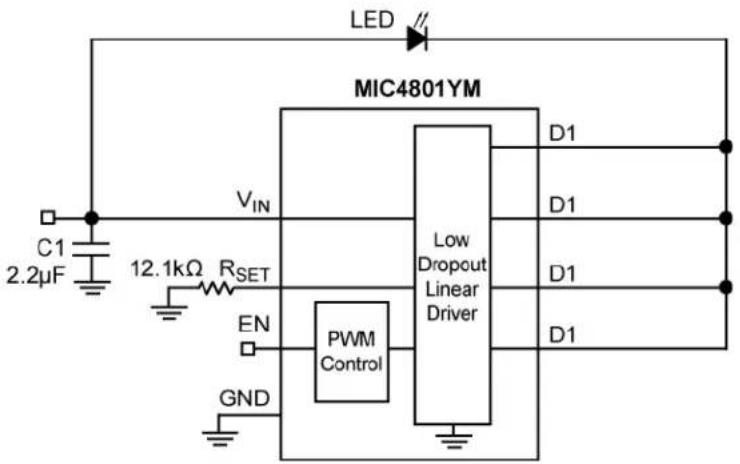
High Current Lighting Schematic
Ultra Fast PWM is a trademark of Micrel, Inc.
Micrel Inc. • 2180 Fortune Drive • San Jose, CA 95131 • USA • tel +1 (408) 944-0800 • fax +1 (408) 474-1000 • http://www.micrel.com
Ordering Information
| Part Number Temperature Range Package | |
| MIC4801YM -40°C to +125°C 8-Pin SOIC |
Pin Configuration

8-Pin SOIC (M) (Top View)
Pin Description
| Pin Number | Pin Name | Pin Function |
| 1 VIN Voltage Input. Connect at least 2.2μF ceramic capacitor between VIN and GND. | ||
| 2 | EN | Enable LED drivers. This pin can be used as a PWM input for dimming of WLEDs. Do not leave floating. |
| 3 | RSET | An internal 1.27V reference sets the nominal maximum WLED current. Example, apply a 12.1kΩ resistor between RSET and GND to set LED current to 416mA at 100% duty cycle. |
| 4 | GND | Ground. |
| 5 | D1 | LED1 driver input. Connect LED anode to VIN and cathode to this pin. All D1 pins must be connected to the LED. |
| 6 | D1 | LED1 driver input. Connect LED anode to VIN and cathode to this pin. All D1 pins must be connected to the LED. |
| 7 | D1 | LED1 driver input. Connect LED anode to VIN and cathode to this pin. All D1 pins must be connected to the LED. |
| 8 | D1 | LED1 driver input. Connect LED anode to VIN and cathode to this pin. All D1 pins must be connected to the LED. |
Absolute Maximum Ratings (1)
Main Input Voltage ( VIN ) -0.3V to +6V
Enable Input Voltage ( VEN )....-0.3V to +6V
LED Driver Voltage ( VD1 ) -0.3V to +6V
Power Dissipation ....Internally Limited
Lead Temperature (soldering, 10sec.)....260°C
Storage Temperature ( Ts ) -65°C to +150°C
Operating Ratings (2)
Supply Voltage ( VIN )....+3.0V to +5.5V
Enable Input Voltage ( VEN ) 0V to VIN
LED Driver Voltage ( VD1 ) 0V to VIN
Junction Temperature ( TJ ) -40°C to +125°C
Junction Thermal Resistance
SOIC-8L JA09....98.9°C/W
Electrical Characteristics
VIN = VEN = 5V, RSET = 12.1kΩ; VD1 = 1.2V; TJ = 25° C, bold values indicate -40° C ≤ TJ ≤ 125° C; unless noted.
| Parameter | Conditions | Min | Typ | ||
| Current\ Accuracy(3) | 374 | 416 | 458 mA | ||
| Drop-out | Where ILED = 90% of LED current seen at VDROP NOM = 1.2V, 100% brightness level | 130 | 250 | mV | |
| Ground/Supply Bias Current | IOUT = 416mA | 2.2 | 2.9 | mA | |
| Shutdown Current | VEN = 0V | 0.01 | 1 | μA | |
| PWM Dimming | |||||
| Enable Input Voltage ( VEN ) | Logic Low | 0.2 | V | ||
| Logic High | 1.2 | V | |||
| Enable Input Current | VIH ≥ 1.2V | 0.01 | 1 | μA | |
| Current Source Delay (50% levels) | Shutdown to on Standby to on On to Standby | 4020.3 | 60 | μsμsμs | |
| Current Source Transient Time (10%-90%) | TRISE TFALL | 10.3 | μsμs | ||
| Stand-by to Shutdown Time | VEN = 0V | 10 | 20 | 40 | ms |
Notes:
- Exceeding the absolute maximum rating may damage the device.
- The device is not guaranteed to function outside its operating rating.
- As determined by average current based on RSET resistance.
Typical Characteristics
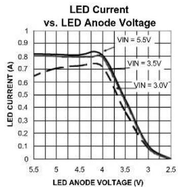

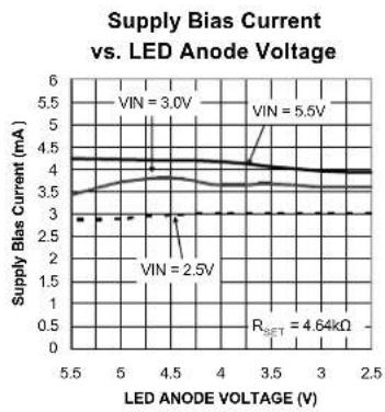


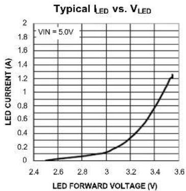
Functional Characteristics


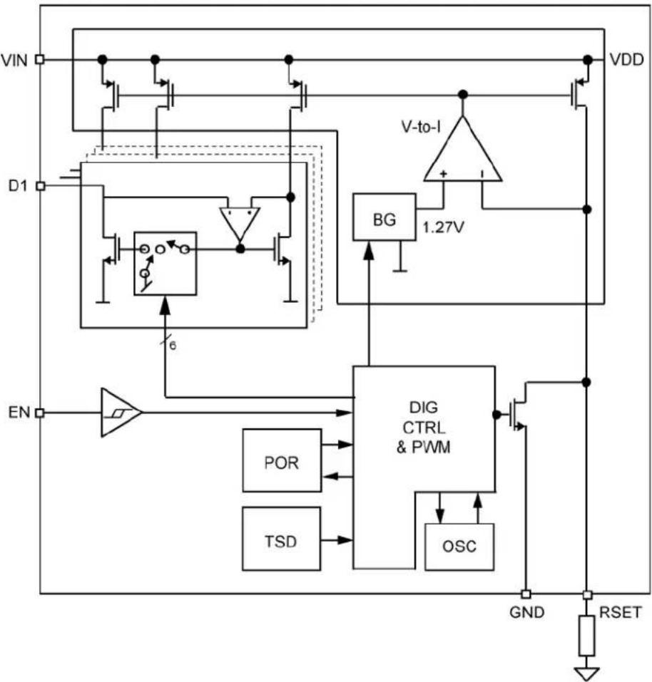
Functional Diagram
Functional Description
The MIC4801 is a single channel linear LED driver with a maximum 600mA current capability. The LED driver is designed to maintain proper current regulation with LED current accuracy of ±10%. The dropout is 130mV at 400mA. The low dropout of the linear drivers allows the LEDs to be driven directly from the battery voltage and eliminates the need for boost or large and inefficient charge pumps. The maximum LED current for each channel is set via an external resistor. Dimming is controlled by applying a PWM signal to the EN pin. The MIC4801 accommodates a wide PWM frequency range as outlined in the application information section.
Block Diagram
As shown in Figure 1, the MIC4801 consists of current mirrors set to copy a master current determined by RSET . The linear LED drivers have a designated control block for enabling and dimming of the LEDs. The MIC4801 dimming is controlled by the Ultra Fast PWM™ control block that receives PWM signals for dimming.
VIN
The input supply ( VIN ) provides power to the linear LED drivers and the control circuitry. The VIN operating range is 3V to 5.5V. A minimum bypass capacitor of 2.2 µ F should be placed close to the input (VIN) pin and the ground (GND) pin. Refer to the layout recommendations section for details on placing the input capacitor (C1).
EN
The EN pin is equivalent to the enable pin for the linear drivers on the MIC4801. It can also be used for dimming by applying a PWM signal. See the PWM Dimming Interface in the Application Information section for details. Pulling the EN low for more than 40ms puts the MIC4801 into a low IQ sleep mode. The EN pin cannot be left floating; a floating enable pin may cause an indeterminate state on the outputs. The first pulse on the EN pin must be equal or greater than 60μs to wake the part up in a known state. This equates to a 8.3kHz PWM signal at equal or greater than 50% duty cycle. Higher PWM frequencies may be used but the first pulse must be equal or greater than 60μs.
RSET
The RSET pin is used to set the peak current of the linear driver by connecting a RSET resistor to ground. The theoretical average LED current can be estimated by equation (1):
I _ LED (mA) = 4 9 2 0* D / R _ SET (kΩ) 1
R _ SET (kΩ) = 4 9 2 0* D / I _ LED (mA) 2
D is the duty cycle of the LED current during PWM dimming. When the device is fully ON the duty cycle equals 100% (D = 1). A plot of ILED versus RSET is shown in Figure 2.
Due to DC losses across current paths internal and external to the package, the calculated RSET resistance equation is modified by a factor K, where K is calculated to be 0.140kΩ.
R _ SET (kΩ) = 4 9 2 0* D / I _ LED (mA) + 0. 1 4 0 (kΩ) 3
I _ LED (mA) = 4 9 2 0* D / ((R _ SET (kΩ) - 0. 1 4 0 (kΩ)) 4
The modified LED current equation is more accurate in determining the actual LED current based on the RSET resistor value.
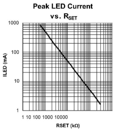
Figure 2. Peak LED Current vs. RSET
D1
The D1 pins are the linear driver inputs for the LED. Connect the anode of the LED to VIN and the cathode to the D1 pins. All the D1 pins must be connected together. The D1 voltage at dropout is the minimum voltage required by the linear driver in order for the LED to be fully biased.
GND
The ground pin is the ground path for the linear driver. The ground of the input capacitor should be routed with low impedance traces to the GND pin and made as short as possible. Refer to the layout recommendations for more details.
Application Information
Ultra Fast PWM™ Dimming Interface
The MIC4801 supports a wide range of PWM control signal frequencies from 200Hz to 500kHz. This extremely wide range of control provides ultimate flexibility for handheld applications using high frequency PWM control signals.
WLED dimming is achieved by applying a pulse width modulated (PWM) signal to the EN pin. For PWM frequencies between 200Hz – 10kHz the MIC4801 supports a duty cycle range from 1% to 100%, as shown in Figure 3. The MIC4801 incorporates an internal shutdown delay to ensure that the internal control circuitry remains active during PWM dimming. This feature prevents the possibility of backlight flickering when using low frequency PWM control signals. The MIC4801 also supports Ultra Fast PWM ™ frequencies from 20kHz to 500kHz. Due to input signal propagation delay, PWM frequencies above 20kHz have a non-linear relationship between the duty cycle and the average LED current, as shown in Figure 3 and 4. Figures 6 through 9 show the WLED current response when a PWM signal is applied to the EN pin (1) .
(1) From the low IQ sleep mode higher PWM frequencies require a logic high enable signal for 60 µ s to first enable the MIC4801 prior to PWM dimming.
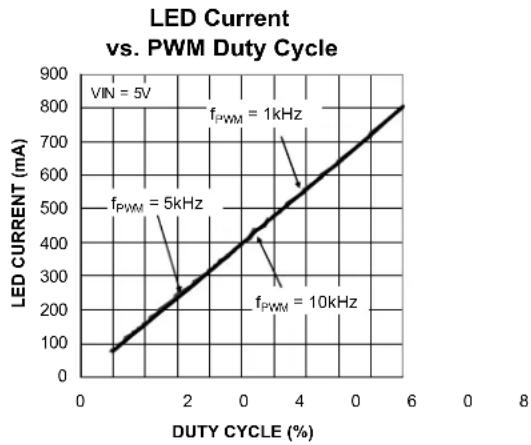
Figure 3. Average Current per LED Dimming by Changing PWM Duty Cycle for PWM Frequencies up to 20kHz
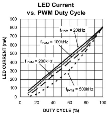
Figure 4. Channel Current Response to PWM Control Signal Frequencies from 50kHz to 500kHz

Figure 5. Minimum Duty Cycle for Varying PWM Frequency

Figure 6. PWM Signal at 1% Duty Cycle ( Iavg = 6mA )

Figure 7. PWM Signal at 20% Duty Cycle ( Iavg = 120mA )

Figure 8. PWM Signal at 50% Duty Cycle ( Iavg = 300mA )

Figure 9. PWM Signal at 80% Duty Cycle ( Iavg = 480mA )
Thermal Consideration
The MIC4801 thermal considerations involve calculating the junction temperature based on the voltage drop across the package and the LED current. The voltage drop across the package is equal to the voltage at D1 with respect to ground times the LED current.
P _ LOSS = I _ LED * V _ D 1
The temperature rise (ΔT) is calculated:
ΔT = P _ LOSS * θ_ JA
Assuming the ILED is 600mA and VD1 is 500mV at 20°C room temperature, we can calculate the junction temperature:
T _ J = T _ A + ΔT
T _ J = 2 0 ^ ° C + 0. 3 W * 9 8. 9 ^ ° C / W
T _ J = 2 0 ^ ° C + 2 9. 7 ^ ° C = 4 9. 7 ^ ° C
The junction temperature will be around 49.7°C.
MIC4801 Typical Application Circuit

Bill of Materials
| Item | Part Number | Manufacturer | Description | |
| C1 | C1608X5R0J225K | TDK(1) | Ceramic Capacitor, 2.2μF, 6.3V, X5R, Size 0603 | 1 |
| 06036D225KAT2A | AVX(2) | |||
| GRM188R60J225KE19D | Murata(3) | |||
| VJ0603G225KXYAT | Vishay(4) | |||
| LED | R42180 | Seoul Semi(5) | Low High Power WLED 1 | |
| R1 | CRCW060312K1FKEA | Vishay(4) Resistor, 1%, 1/16W, Size 0603 1 | ||
| U1 | MIC4801YM | Micrel, (6) | 600mA Single Channel Ultra Fast PWM TM Inc. Linear WLED Driver | 1 |
Notes:
- TDK: www.tdk.com
- AVX: www.avx.com
- Murata: www.murata.com
- Vishay: www.vishay.com
- Seoul Semi: http://www.acriche.com/en
- Micrel, Inc.: www.micrel.com
Qty.
Layout Recommendations

Top Layer

Bottom Layer
Package Information
![0.236±0.008 [5.99±0.21] PIN #1 ID MARK 0.194 +0.002 -0.005 [4.93 +0.05] -0.13](/content/2026/06/1248557/images/344541e5e5777e85eba4fb048d5320c70116c3f7145aaa76dd9ae9e7806b1e7b.jpg)
TOP VIEW
![BOTTOM MARK 0.085-0.100 DIA. 0.016 +0.0032 -0.0028 [0.41 +0.09] -0.06] 0.050[1.27] BSC](/content/2026/06/1248557/images/1db0b1541b522ea3574528e9d48c0102cbf1e92c66bb44a41714e74b385b0e91.jpg)
BOTTOM VIEW
![0.064 +0.004 -0.010 [1.63 -0.254] (A) SEE DETAIL *A* 0.013 +0.007 -0.003 ×45* [0.33 -0.17] -0.08] 0.008 +0.0018 -0.005 [0.20 -0.01] 0.006 +0.004 -0.002 [0.15 -0.16] -0.05 0.155 +0.002 -0.005 [3.94 -0.13] -0.13 3](/content/2026/06/1248557/images/3c71816d4063e34e832d3c47c10410553f84bd0659670de7f4fda89b3dc9245e.jpg)
END VIEW
![-C- 0.004[0.10] 5° +3° -5° 0.025 +0.025 -0.009 [0.64 -0.63] -0.23]](/content/2026/06/1248557/images/ab833d911053480b3cba8ad9aa6acb16bc5e2bb604f6c5baf9e8ad88b0e66072.jpg)
DETAIL "A"
8-Pin SOIC (M)
MICREL, INC. 2180 FORTUNE DRIVE SAN JOSE, CA 95131 USA
TEL +1 (408) 944-0800 FAX +1 (408) 474-1000 WEB http://www.micrel.com
Micrel makes no representations or warranties with respect to the accuracy or completeness of the information furnished in this data sheet. This information is not intended as a warranty and Micrel does not assume responsibility for its use. Micrel reserves the right to change circuitry, specifications and descriptions at any time without notice. No license, whether express, implied, arising by estoppel or otherwise, to any intellectual property rights is granted by this document. Except as provided in Micrel's terms and conditions of sale for such products, Micrel assumes no liability whatsoever, and Micrel disclaims any express or implied warranty relating to the sale and/or use of Micrel products including liability or warranties relating to fitness for a particular purpose, merchantability, or infringement of any patent, copyright or other intellectual property right.
Micrel Products are not designed or authorized for use as components in life support appliances, devices or systems where malfunction of a product can reasonably be expected to result in personal injury. Life support devices or systems are devices or systems that (a) are intended for surgical implant into the body or (b) support or sustain life, and whose failure to perform can be reasonably expected to result in a significant injury to the user. A Purchaser's use or sale of Micrel Products for use in life support appliances, devices or systems is a Purchaser's own risk and Purchaser agrees to fully indemnify Micrel for any damages resulting from such use or sale.
© 2010 Micrel, Incorporated.
- HIGH EFFICIENCY 600MA SINGLE CHANNEL LINEAR WLED DRIVER WITH ULTRA FAST PWM™ CONTROL
- GENERAL DESCRIPTION
- FEATURES
- APPLICATIONS
- TYPICAL APPLICATION
- ABSOLUTE MAXIMUM RATINGS (1)
- OPERATING RATINGS (2)
- ELECTRICAL CHARACTERISTICS
- NOTES
- FUNCTIONAL DIAGRAM
- FUNCTIONAL DESCRIPTION
- BLOCK DIAGRAM
- VIN
- EN
- RSET
- D1
- GND
- APPLICATION INFORMATION
- ULTRA FAST PWM™ DIMMING INTERFACE
- THERMAL CONSIDERATION
- MIC4801 TYPICAL APPLICATION CIRCUIT
- BILL OF MATERIALS
- LAYOUT RECOMMENDATIONS
- PACKAGE INFORMATION
- MICREL, INC. 2180 FORTUNE DRIVE SAN JOSE, CA 95131 USA
Brand : Microchip
Model : MIC4801
Category : LED driver