11AA02E48 - Spécification de bus Microchip - Free user manual and instructions
Find the device manual for free 11AA02E48 Microchip in PDF.

User questions about 11AA02E48 Microchip
0 question about this device. Answer the ones you know or ask your own.
Ask a new question about this device
Download the instructions for your Spécification de bus in PDF format for free! Find your manual 11AA02E48 - Microchip and take your electronic device back in hand. On this page are published all the documents necessary for the use of your device. 11AA02E48 by Microchip.
USER MANUAL 11AA02E48 Microchip
Note the following details of the code protection feature on Microchip devices:
• Microchip products meet the specification contained in their particular Microchip Data Sheet.
- Microchip believes that its family of products is one of the most secure families of its kind on the market today, when used in the intended manner and under normal conditions.
- There are dishonest and possibly illegal methods used to breach the code protection feature. All of these methods, to our knowledge, require using the Microchip products in a manner outside the operating specifications contained in Microchip's Data Sheets. Most likely, the person doing so is engaged in theft of intellectual property.
• Microchip is willing to work with the customer who is concerned about the integrity of their code.
- Neither Microchip nor any other semiconductor manufacturer can guarantee the security of their code. Code protection does not mean that we are guaranteeing the product as "unbreakable."
Code protection is constantly evolving. We at Microchip are committed to continuously improving the code protection features of our products. Attempts to break Microchip's code protection feature may be a violation of the Digital Millennium Copyright Act. If such acts allow unauthorized access to your software or other copyrighted work, you may have a right to sue for relief under that Act.
Information contained in this publication regarding device applications and the like is provided only for your convenience and may be superseded by updates. It is your responsibility to ensure that your application meets with your specifications. MICROCHIP MAKES NO REPRESENTATIONS OR WARRANTIES OF ANY KIND WHETHER EXPRESS OR IMPLIED, WRITTEN OR ORAL, STATUTORY OR OTHERWISE, RELATED TO THE INFORMATION, INCLUDING BUT NOT LIMITED TO ITS CONDITION, QUALITY, PERFORMANCE, MERCHANTABILITY OR FITNESS FOR PURPOSE. Microchip disclaims all liability arising from this information and its use. Use of Microchip devices in life support and/or safety applications is entirely at the buyer's risk, and the buyer agrees to defend, indemnify and hold harmless Microchip from any and all damages, claims, suits, or expenses resulting from such use. No licenses are conveyed, implicitly or otherwise, under any Microchip intellectual property rights.
Trademarks
The Microchip name and logo, the Microchip logo, dsPIC, KEELOQ, KEELOQ logo, MPLAB, PIC, PICmicro, PICSTART, rfPIC and UNI/O are registered trademarks of Microchip Technology Incorporated in the U.S.A. and other countries.
FilterLab, Hampshire, HI-TECH C, Linear Active Thermistor, MXDEV, MXLAB, SEEVAL and The Embedded Control Solutions Company are registered trademarks of Microchip Technology Incorporated in the U.S.A.
Analog-for-the-Digital Age, Application Maestro, CodeGuard, dsPICDEM, dsPICDEM.net, dsPICworks, dsSPEAK, ECAN, ECONOMONITOR, FanSense, HI-TIDE, In-Circuit Serial Programming, ICSP, Mindi, MiWi, MPASM, MPLAB Certified logo, MPLIB, MPLINK, mTouch, Octopus, Omniscient Code Generation, PICC, PICC-18, PICDEM, PICDEM.net, PICkit, PICtail, PIC ^32 logo, REAL ICE, rfLAB, Select Mode, Total Endurance, TSHARC, UniWinDriver, WiperLock and ZENA are trademarks of Microchip Technology Incorporated in the U.S.A. and other countries.
SQTP is a service mark of Microchip Technology Incorporated in the U.S.A.
All other trademarks mentioned herein are property of their respective companies.
© 2009, Microchip Technology Incorporated, Printed in the U.S.A., All Rights Reserved.
Printed on recycled paper.
QUALITY MANAGEMENT SYSTEM
CERTIFIED BY DNV
=ISO/TS 16949:2002=
Microchip received ISO/TS-16949:2002 certification for its worldwide headquarters, design and wafer fabrication facilities in Chandler and Tempe, Arizona; Gresham, Oregon and design centers in California and India. The Company's quality system processes and procedures are for its PIC® MCUs and dsPIO® DSCs, KEELOO® code hopping devices, Serial EEPROMs, microperipherals, nonvolatile memory and analog products. In addition, Microchip's quality system for the design and manufacture of development systems is ISO 9001:2000 certified.
Table of Contents
1.0 Introduction 5
2.0 General Characteristics 8
3.0 Standby Pulse 9
4.0 Bit-Level Definition 10
5.0 Byte-Level Definition 11
6.0 Start Header 12
7.0 8-Bit Device Addressing 13
8.0 12-Bit Device Addressing 14
9.0 Command Structure 15
10.0 Device Address Polling 16
11.0 Device Modes 17
12.0 Electrical Specifications 18
NOTES:
UNI/O ^® Bus Specification
1.0 INTRODUCTION
As embedded systems become smaller, there exists a growing need to minimize I/O signal consumption for communication between devices. Microchip has addressed this need by developing the patented** UNI/O® bus, a low-cost, easy-to-implement solution requiring only a single I/O signal for communication.
UNI/O bus-compatible devices can be used to enhance any application facing restrictions on available I/O. Such restrictions can possibly stem from connectors, board space, or from the master device itself.
1.1 Description
The UNI/O bus provides the definition for communication through a single I/O signal. It supports the use of multiple devices through a "bussed" system.
One device is defined as the master and is responsible for initiating and coordinating all operations with the slave devices on the bus. Each slave acts as a peripheral to the master and a slave can be designed for any number of purposes.
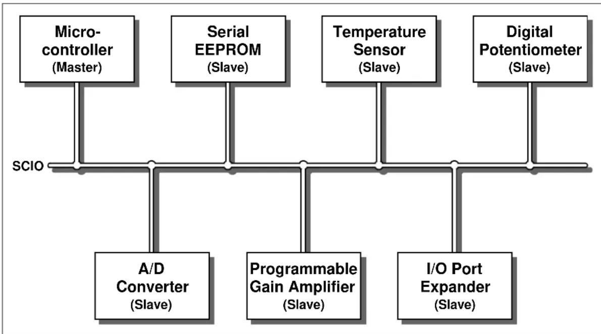
Figure 1-1 shows an example system with a microcontroller acting as the master, and other numerous devices attached to the bus as slave peripherals. Note that the master is not limited to being a microcontroller, but can be any device capable of processing the necessary I/O signal.
Data is embedded into the I/O stream through Manchester encoding. The bus is controlled by the master which determines the clock period, controls the bus access and initiates all operations, while all other devices act as slaves. Both master and slave devices can operate as transmitter or receiver, but the master determines which mode is active.
The UNI/O bus supports operation from 10 kbps to 100 kbps (equivalent to 10 kHz to 100 kHz) and places no restrictions on voltage ranges, temperature ranges, or manufacturing processes.
FIGURE 1-1: UNI/O ^® BUS EXAMPLE
flowchart
graph TD
    A["Micro-controller (Master)"] --> B["SCIO"]
    C["Serial EEPROM (Slave)"] --> B
    D["Temperature Sensor (Slave)"] --> B
    E["Digital Potentiometer (Slave)"] --> B
    B --> F["A/D Converter (Slave)"]
    B --> G["Programmable Gain Amplifier (Slave)"]
    B --> H["I/O Port Expander (Slave)"]
**UNI/O® is a registered trademark of Microchip Technology Inc. Microchip's UNI/O Bus products are covered by the following patent issued in the U.S.A.: 7,376,020.
1.2 Definitions
1.2.1 SCIO
SCIO is the only I/O signal required for the UNI/O bus. Both the serial clock and data are embedded together through Manchester encoding. In this encoding method, each bit consists of a mandatory edge in the middle of a bit period. The direction of this edge determines the value of the bit. A rising edge indicates a '1', whereas a falling edge indicates a '0'.
1.2.2 MASTER DEVICE
The master device determines the clock period, controls bus access and initiates all operations. Only one master is allowed in a system. Examples of master devices include microcontrollers, ASICs and FPGAs.
1.2.3 SLAVE DEVICE
A slave device acts as a peripheral on the bus. Slaves do not initiate any operations; they merely respond to operations begun by the master. Each slave must have a unique device address with which the master can select the device. Slave devices can operate as both transmitter and receiver, but the mode is determined by the master in conjunction with the command issued. Examples of slave devices include serial EEPROMs, temperature sensors and A/D converters.
1.2.4 TRANSMITTER
The transmitter is defined as the device with control of the bus during transmission of a byte. For example, while data is outputting from a slave to the master, the slave is acting as the transmitter.
1.2.5 RECEIVER
The receiver is defined as the device receiving the current byte of data. For example, while a command is being transmitted to a slave from the master, the slave is acting as the receiver.
1.2.6 BIT PERIOD
The bit period is defined as the amount of time reserved for transmission of a single bit. This time period is determined by the master. All slaves recover this period through the start header by measuring the amount of time needed to send the header.
For each bit, the Manchester-encoded bit edge must occur at the middle of the bit period.
1.2.7 STANDBY PULSE
The high pulse used to place all slave devices into Standby mode is called the standby pulse. It is required at the beginning of a command when selecting a new device.
1.2.8 START HEADER
The start header is the combination of a short low pulse followed by a header byte of the value '01010101'. This is always the first byte transmitted for any given command.
After the header byte has been sent, an Acknowledge sequence is performed. For this specific sequence only, no slave responds during the normal SAK time.
1.2.9 DEVICE ADDRESS
Following the start header, the device address is sent. This can consist of either one or two bytes, depending on whether 8-bit or 12-bit device addressing is supported, respectively. The purpose of the device address is to select a specific slave device on the bus. For this reason, every slave device in a system must have a unique device address. Otherwise, bus conflicts will occur and operation will be undefined.
1.2.10 FAMILY CODE
The family code is a 4-bit value included in the device address and indicates the family in which the device resides. Examples of device families include memory devices, temperature sensors and A/D converters.
1.2.11 DEVICE CODE
The device code is either a 4- or 8-bit value, depending on whether 8-bit or 12-bit device addressing is supported, respectively. It is used to differentiate devices with the same family code. Some devices may support programmable device code bits, whereas on others they may be fixed.
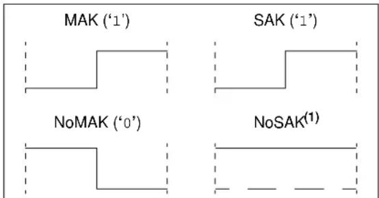
After each byte is transmitted, a 2-bit Acknowledge sequence is performed. The first bit is for the MAK and the second bit is for the SAK. The sequence is used to indicate continuation or termination of an operation, as well as to confirm reception of a byte.
1.2.13 MAK/NOMAK
The MAK bit occurs as the first bit of every Acknowledge sequence. It is always sent by the master, regardless of which device transmitted the preceding byte. A MAK is sent as a '1', and a NoMAK as a '0'.
Sending a MAK during an Acknowledge sequence indicates that the current operation is to be continued. This means that more data is to be sent by the device acting as transmitter. A NoMAK indicates that the current operation is to be terminated immediately following the Acknowledge sequence.
1.2.14 SAK/NOSAK
The SAK bit occurs as the second bit of the Acknowledge sequence and is sent strictly by the slave device regardless of which device transmitted the preceding byte. A SAK is sent as a '1', and a NoSAK appears as no edge at all (i.e., no device transmitting).
A NoSAK will occur after each full byte that is transmitted before the end of the device address. For example, for 8-bit addressing, a NoSAK will occur after the start header only, and for 12-bit addressing, a NoSAK will occur after both the start header and the MSB of the device address.
1.2.15 IDLE MODE
Idle mode is a device mode during which a slave device ignores all serial communication until the reception of a standby pulse. Slave devices enter this mode after release from POR, as well as any time an error condition occurs.
1.2.16 STANDBY MODE
Standby mode is a low-power device mode during which a slave device awaits a high-to-low transition on SCIO, marking the beginning of the start header. Slave devices enter this mode upon reception of a standby pulse and after the successful termination of a command via a NoMAK/SAK combination.
1.2.17 HOLD MODE
Hold provides a method for the master to pause serial communication in order to service interrupts or perform other necessary functions. Hold mode is entered by holding SCIO low during any given MAK bit period and is exited by performing a standard Acknowledge sequence with a MAK bit.
Hold mode is not required to be implemented on all slave devices.
2.0 GENERAL CHARACTERISTICS
There is only a single I/O signal, SCIO, necessary for communication between devices and all data transmission occurs through this line. The SCIO signal for all devices in a system are connected together directly in a bussed configuration. The Idle state of the bus is high. In order to ensure the bus is in the Idle state during times when the master may not be driving the bus, the use of a pull-up resistor is recommended. Both clock and data are embedded together by way of Manchester encoding.
The serial stream is divided into bit periods, with one data bit being embedded per period. The bit period time is determined by the master and communicated to the slave during the start header at the beginning of each command. Therefore, the bit period must only be consistent within a single command.
2.1 Bit Rate
Parameter FBIT in Table 12-2 defines the currently supported frequency range. Note that, due to the asynchronous nature of the bus, both minimum and maximum frequencies are defined.
2.2 Voltage Range
In order to support a wide number of fabrication processes, no limitation has been defined for the operating voltages of devices attached to the bus. Such ranges are dependent solely on the specific devices. The only requirement is that input threshold voltages and output current limits meet the electrical specifications set forth in Table 12-1.
2.3 I/O Structures
The I/O structure for SCIO consists of an input buffer and a tri-stateable, push-pull output driver. To avoid high currents during possible bus contention, and to refrain from requiring external components, the SCIO output driver on all slave devices must be current-limited to the specifications listed in Table 12-1. If the output driver on the master device in a system is not significantly stronger than on the slave devices, ambiguous voltage levels may occur during times of possible bus contention.
Because the bus Idle state is high, a pull-up resistor is recommended to ensure bus idle during power up/down sequences, as well as any other time in which no device is driving the bus.
2.4 Bus Capacitance
Successful communication is dependant upon edge transitions occurring within the proper time frames. Moreover, slew rates must be minimized to avoid detecting unwanted edges, most critically during the start header. Because of this, the bus capacitance is limited to 100 pF. This is comprised of the SCIO pin capacitance for all devices on the bus, as well as the capacitance of all wires and connections.
2.5 Fabrication Processes
The UNI/O bus is not designed for any particular process or technology. Therefore, all IC fabrication technologies are supported, so long as the electrical specifications set forth in Section 12.0 “Electrical Specifications” are met.
3.0 STANDBY PULSE
Before communicating with a new device, a standby pulse must be performed. This pulse signals to all slave devices on the bus to enter Standby mode, awaiting a new command to begin. The standby pulse can also be used to prematurely terminate a command.
The standby pulse consists of holding SCIO high for a minimum of TSTBY. After this has been performed, the slave devices will be ready to receive a command.
Once a command is terminated satisfactorily (i.e., via a NoMAK/SAK combination during the Acknowledge sequence), performing a standby pulse is not required to begin a new command as long as the device to be selected is the same device selected during the previous command. In this case, a period of Tss must be observed after the end of the command and before the beginning of the start header. After Tss, the start header (including low pulse) can be transmitted in order to begin the new command.
If a command is terminated in any manner other than a NoMAK/SAK combination, or if an invalid number of data bytes has been sent (as specified by the command's definition), then this is considered an error condition and the master must perform a standby pulse before beginning a new command, regardless of which device is to be selected.
An example of two consecutive commands is shown in Figure 3-1. Note that the device address is the same for both commands, indicating that the same device is being selected both times.
Note: After a POR/BOR event occurs, a low-to-high transition on SCIO must be generated before proceeding with any communication, including a standby pulse.
FIGURE 3-1: CONSECUTIVE COMMANDS EXAMPLE

text_image
Standby Pulse Start Header MAK NoSAK Device Address MAK SAK SCIO 0101:0 0 00 00101 NoMAK SAK TSS Start Header MAK NoSAK Device Address MAK SAK SCIOUpon detection of the standby pulse, a slave device will typically enter its lowest power state. The exception to this is when the slave device is executing an internal process in the background. Examples include an EEPROM performing a write cycle, or a temperature sensor carrying out a conversion.
If at any point during a command an error is detected by the master, a standby pulse should be generated and the command should be performed again.
4.0 BIT-LEVEL DEFINITION
Clock and data are embedded together through Manchester encoding. Each data bit is transmitted within a single bit period, TE, which is specified by the master during the start header of the command.
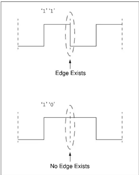
Every bit period includes an edge transition at the middle of the period, and it is the direction of this edge which determines the value of the bit. A rising middle edge indicates a '1' value, whereas a falling edge indicates a '0', as shown in Figure 4-1.
FIGURE 4-1: BIT VALUES

text_image
'1' '0' TE TEBecause every bit period must have a middle edge transition, there may or may not exist another edge transition at the beginning of a bit period. This is entirely dependent upon the values of both the previous and current bits. If two bits of equal value are being successively transmitted, then a transition at the beginning of the second bit is required. If the two bits are of opposing values, then no edge will occur. Refer to Figure 4-2 for details.
FIGURE 4-2: SUCCESSIVE BIT
TRANSMISSION
EXAMPLE
text_image
'1' '1' Edge Exists '1' '0' No Edge Exists4.1 Timing Considerations
In order to allow for flexibility in timing, UNI/O bus-compatible devices must be tolerant of small deviations, or jitter, in input edge timing, as specified by TIJIT. See Figure 12-4 for details.
Slave devices must also allow for a small amount of frequency drift. FDRIFT specifies the maximum drift per byte tolerance required for all slave devices, and FDEV shows the overall drift from the initial serial bit period for a single command. For example, if a command is begun using a 20 s bit period, the master can drift a maximum of 20 s*FDRIFT per byte, up to a total of 20 s*FDEV within that command.
5.0 BYTE-LEVEL DEFINITION
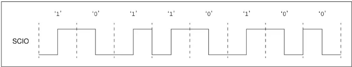
Communication is formatted using 8-bit bytes. All bytes are transmitted with the Most Significant bit sent first and the Least Significant bit sent last. Each bit is transmitted immediately following the previous bit, with no delay in between bits. An example is shown in Figure 5-1.
FIGURE 5-1: BYTE TRANSMISSION EXAMPLE
text_image
SCIO '1' '0' '1' '1' '0' '1' '0'5.1 Acknowledge Sequence
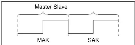
An Acknowledge routine occurs after each byte is transmitted, including the start header. This routine consists of two bits. The first bit is transmitted by the master and the second bit is transmitted by the slave, as shown in Figure 5-2.
5.1.1 MAK
The Master Acknowledge, or MAK, is signified by transmitting a '1' and informs the slave that the command is to be continued (i.e., more data will be sent). Conversely, a Not Acknowledge, or NoMAK, is signified by transmitting a '0', as shown in Figure 5-3, and is used to end the current command and initiate any corresponding internal processing, if necessary.
A MAK must always be transmitted following the start header. If a NoMAK is transmitted, device operation will be undefined.
5.1.2 SAK
The Slave Acknowledge, or SAK, is also signified by transmitting a '1' and confirms successful reception of the previous byte of data. Unlike the NoMAK, the NoSAK is signified by the lack of a middle edge during the bit period.
In order to avoid possible bus collision due to multiple devices transmitting at the same time, no slave device will respond with a SAK until a specific slave has been selected. That is, a NoSAK will occur after each byte that is transmitted before the end of the device address (i.e., for 8-bit addressing, a NoSAK occurs after the start header only, and for 12-bit addressing, a NoSAK occurs after both the start header and the MSB of the device address).
5.1.3 ERROR DETECTION
If a SAK is not received from the slave after any byte (after a device has been selected), an error has occurred. The master should then perform a standby pulse and begin the desired command again.
FIGURE 5-2: ACKNOWLEDGE ROUTINE
flowchart
graph TD
    A["Master Slave"] --> B["MAK"]
    A --> C["SAK"]
FIGURE 5-3: ACKNOWLEDGE BITS
flowchart
graph TD
    A["MAK ('1')"] --> B["NoMAK ('0')"]
    C["SAK ('1')"] --> D["NoSAK(1)"]
    E["NoMAK ('0')"] --> F["NoSAK(1)"]
Note 1: A NoSAK is defined as any sequence that is not a valid SAK.
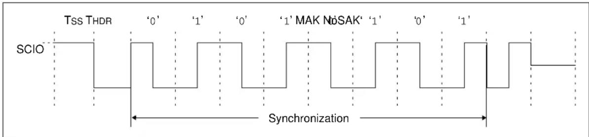
6.0 START HEADER
All operations must be preceded by a start header. The start header consists of holding SCIO low for a period of THDR, followed by transmitting an 8-bit '01010101' code. This code is used to synchronize the slave's internal clock period with the master's clock period, so accurate timing is very important. An Acknowledge sequence is then performed following transmission of the start header. Figure 6-1 shows an example of the start header sequence.
When a standby pulse is not required (i.e., between successive commands to the same device), a period of Tss must be observed after the end of the command and before the beginning of the start header.
FIGURE 6-1: START HEADER EXAMPLE
text_image
TSS THDR '0' '1' '0' '1' MAK NoSAK' '1' '0' '1' SCIO SynchronizationDuring the Acknowledge sequence following the start header, no slave device will respond with a SAK. Within this time, the bus will not be driven by any device and no edge transition will occur. Refer to Section 5.1 "Acknowledge Sequence" for details.
6.1 Synchronization
6.1.1 OSCILLATOR
In order to provide an accurate time base with which to extract the serial clock frequency, an oscillator must be used by each slave device on the bus. This can be either internal or external to the device, though including an internal oscillator is strongly recommended to avoid requiring excess external components.
The necessary accuracy of the oscillator to a specific frequency is dependent only on the design of the device. The only bus-based requirements are that the chosen oscillator be stable enough across voltage and temperature and that the frequency is high enough to provide a reasonable state of synchronization during a command.
If an internal oscillator is included, it is recommended that it be powered down during Idle and Standby modes so as to reduce unnecessary power consumption. The THDR period provides a time during which such an internal oscillator can power-up and stabilize.
6.1.2 SERIAL FREQUENCY EXTRACTION
The start header is utilized by slave devices as a means of determining the bit period used by the master. During the start header, a counter can be used to measure the amount of time required to transmit 8 bits of data. This counter can then be divided down to determine the bit period, TE, which can be used as a comparison for all other bits.
The required widths of such counters are dependent upon the oscillator frequency used and would need to be wide enough to support 100 s bit periods (10 kbps operation).
6.2 Re-synchronization
During communication, it is possible that either the master's or the slave's reference clock may drift. This may be due to many events, including changes in voltage or temperature. If not corrected for, such a drift will eventually cause a loss of synchronization. Therefore, all slave devices must monitor the middle edge of each MAK bit and where it occurs relative to the slave's bit period, and then adjust its frequency to match.
6.2.1 PHASE ADJUSTMENT
During every MAK bit, the middle edge should also be used to reset the slave's phase (i.e., the slave should assume that the MAK edge is located at the middle of the master's bit period and therefore use it as a reference for further communication).
This will ensure that any error in phase which may occur will not accumulate from byte to byte.
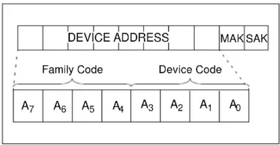
7.0 8-BIT DEVICE ADDRESSING
In order to differentiate individual slave devices on the bus, a device address byte is sent by the master device following the start header. This is an 8-bit value used to select a specific device attached to the bus.
The device address byte consists of a 4-bit family code and a 4-bit device code. The device code may be either fixed or programmable in order to provide the ability to cascade multiple devices with identical family codes on the same bus.
FIGURE 7-1: 8-BIT DEVICE ADDRESS
flowchart
graph TD
    A["Device Code"] --> B["Family Code"]
    B --> C["Device Code"]
    C --> D["MAK"]
    C --> E["SAK"]
    F["Device Address"] --> G["A7"]
    H["Device Code"] --> I["A6"]
    J["Device Code"] --> K["A5"]
    L["Device Code"] --> M["A4"]
    N["Device Code"] --> O["A3"]
    P["Device Code"] --> Q["A2"]
    R["Device Code"] --> S["A1"]
    T["Device Code"] --> U["A0"]
7.1 Family Code
The upper nibble (bits A_7-A_4 ) of the device address is the family code. This code is a 4-bit value and specifies in which family the device resides. The families and codes are defined by Microchip and must be followed in order to reduce the risk of address conflicts. To obtain the proper code for a specific device, please contact Microchip.
Certain codes have been reserved for special functions and are listed in Table 7-1.
TABLE 7-1: RESERVED FAMILY CODES
| Code | Description |
| ‘0000’ | Reserved for future use |
| ‘0011’ | Display Controllers |
| ‘0100’ | I/O Port Expanders |
| ‘1000’ | Frequency/Quadrature/PWM Encoders, Real-Time Clocks |
| ‘1001’ | Temperature Sensors |
| ‘1010’ | EEPROMs |
| ‘1011’ | Encryption/Authentication Devices |
| ‘1100’ | DC/DC Converters |
| ‘1101’ | A/D Converters |
| ‘1111’ | 12-bit Addressable Devices |
7.2 Device Code
The lower nibble (bits A_3-A_0 ) of the device address is the device code. This code is a 4-bit value and is used to differentiate between multiple devices on the bus within the same family. The device code is defined at the device level and can be either fixed or customizable. Such customizable bits can be implemented in any manner, including via external input pins or software configuration.
It is strongly recommended that as many customizable device code bits as possible be included in order to help avoid address conflicts.
8.0 12-BIT DEVICE ADDRESSING
As an extension to 8-bit device addressing (Section 7.0 "8-Bit Device Addressing"), 12-bit device addressing allows for support of a much larger number of devices. Devices designed to support 12-bit addressing are fully compatible with 8-bit addressable devices, and both can be connected onto the bus concurrently.
The 12-bit device addressing scheme takes advantage of the '1111' family code defined in Section 7.1 "Family Code". This code functions as an enable for 12-bit addressing compatible devices and will place all other devices into Idle mode.
FIGURE 8-1: 12-BIT DEVICE ADDRESS

flowchart
graph TD
    subgraph DeviceCode
        A1["Device Code A7"] --> A6["Device Code A6"]
        A5["Device Code A5"] --> A4["Device Code A4"]
        A3["Device Code A3"] --> A2["Device Code A2"]
        A2["Device Code A2"] --> A1["Device Code A1"]
        A0["Device Code A0"] --> A0a["A0"]
    end
    subgraph FamilyCode
        A11["1A11"] --> A10["A10"]
        A9["A9"] --> A8["A8"]
    end
    subgraph 12-BitAddressCode
        B1["12-Bit Address Code"] --> B11["Family Code"]
        B11 --> B10
        B10 --> B9["A9"]
        B9 --> B8["A8"]
    end
    subgraph MAK
        C1["MAK"] --> C2["No SAK"]
        C2 --> C3["DEVICE LOW ADDRESS"]
        C3 --> C4["DEVICE"]
    end
    subgraph MAKSAK
        D1["MAK"] --> D2["SAK"]
    end
8.1 Family Code
The lower nibble (bits A_11-A_8 ) of the device high address is the family code. This code is a 4-bit value and specifies in which family the device resides. The families and codes are defined by Microchip and must be followed in order to reduce the risk of address conflicts. To obtain the proper code for a specific device, please contact Microchip.
Certain codes have been reserved for special functions and are listed in Table 8-1.
TABLE 8-1: FAMILY CODES
| Code Description |
| '0000' Reserved for future use |
| '1111' Reserved for future use |
8.2 Device Code
The low byte (bits A_7-A_0 ) of the device address is the device code. This code is an 8-bit value and is used to differentiate between multiple devices on the bus within the same family. The device code is defined at the device level and can be either fixed or customizable. Such customizable bits can be implemented in any manner, including via external input pins or software configuration.
It is strongly recommended that as many customizable device code bits as possible be included in order to help avoid address conflicts.
9.0 COMMAND STRUCTURE
After the device address, a command byte must be sent by the master to indicate the type of operation to be performed. This command is defined at the device level and no restrictions are placed on it by the bus.
A full operation can consist of any number of bytes, ranging from a single command byte to a theoretically unlimited maximum. After the initial command byte, additional bytes can be included for any necessary purpose, such as for addressing or data.
Regardless of the number of bytes required, all commands are terminated through the transmission of a NoMAK from the master.
A full operation consists of the following steps:
- Standby Pulse (1)
- Start Header
- Device Address
- Command Byte
- Any other bytes necessary for the operation
Note 1: A standby pulse may not be required for consecutive commands to the same device. Refer to Section 3.0 “Standby Pulse” for more details.
Figure 9-1 shows an example read operation for a serial EEPROM.
FIGURE 9-1: EXAMPLE EEPROM READ OPERATION

text_image
Standby Pulse Start Header MAK NoSAK Device Address MAK SAK SCIO 01 01 00 1 0 A3 A2 A1 A0 0 Command MAK SAK Word Address MSB MAK SAK Word Address LSB MAK SAK SCIO 15 14 13 12 11 10 9 8 7 6 5 4 3 2 1 0 0 0 0 0 0 1 Data Byte 1 MAK SAK Data Byte 2 MAK SAK Data Byte n MAK SAK SCIO 7 6 5 4 3 2 1 0 7 6 5 4 3 2 1 0 7 6 5 4 3 2 1 0 NoMAK SAK10.0 DEVICE ADDRESS POLLING
Slave devices must respond with a SAK if either a MAK or NoMAK is received following the device address, as long as the address is valid. In the case of a NoMAK, the slave device will return to Standby mode immediately following the transmission of the SAK.
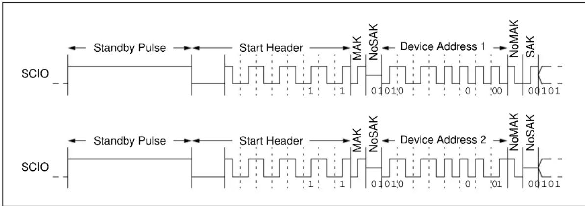
This feature allows the master to perform an address polling sequence in order to determine what devices are connected to the bus. Such a sequence is typically used in conjunction with a list of expected device addresses to allow for added flexibility in system design.
In order to perform device address polling, the master generates a standby pulse and start header and transmits the desired device address followed by a NoMAK. The master then checks to see whether or not a corresponding slave transmits a SAK. If a SAK is received, then a slave exists with the specified device address. Note that a standby pulse must be generated before every command, as a different device is being addressed during each sequence.
Figure 10-1 shows an example of polling for two devices, both with 8-bit device addresses. In this example, the first device exists on the bus and the second device does not exist. For 12-bit addressing, the sequence is the same except that the SAK is checked following the device low address.
FIGURE 10-1: DEVICE ADDRESS POLLING EXAMPLE
text_image
Standby Pulse Start Header MAK NoSAK Device Address 1 NoMAK SAK SCIO 01010 00 00101 Standby Pulse Start Header MAK NoSAK Device Address 2 NoMAK NoSAK SCIO11.0 DEVICE MODES
11.1 Device Idle
Slave devices must feature a Idle mode during which all serial data is ignored until a standby pulse occurs. Idle mode will be entered, without generation of a SAK, upon the following conditions:
- Invalid Device Address
- Invalid command byte
- Missed edge transition (except when entering Hold)
- Reception of a NoMAK before completing a command sequence, except following a device address
An invalid start header cannot be detected, but will indirectly also cause the device to enter Idle mode by preventing the slave from synchronizing properly with the master. If the slave is not synchronized with the master, an edge transition will be missed, thus causing the device to enter Idle mode.
11.2 Device Standby
Slave devices must feature a Standby mode during which the device is waiting to begin a new command. After observing the Tss time period, a high-to-low transition on SCIO will exit Standby and prepare the device for reception of the start header.
Standby mode will be entered upon the following conditions:
- A NoMAK followed by a SAK (i.e., valid termination of a command)
- Reception of a standby pulse
Standby mode can be used to provide a low-power mode of operation. In order to maximize power efficiency, such a mode should be interrupted only at the beginning of the low pulse of the start header.
11.3 Device Hold
Hold mode allows the master to suspend communication in order to perform other tasks, such as servicing interrupts, etc. In order to initiate the Hold sequence, the master must bring SCIO low at the beginning of the next MAK bit period for a minimum time of THLD and continue to keep it low while in hold.
To bring the slave out of hold, the master continues the current operation, starting with an Acknowledge sequence as described in Section 5.1 "Acknowledge Sequence", transmitting a MAK and checking for the slave response. See Figure 11-1 for more details. The Acknowledge sequence need not be in phase with previously transmitted bits, thereby allowing the Hold sequence to last for any length of time greater than THLD. The bit period must remain constant throughout the hold sequence.
Note that if SCIO is held low for a full bit period (i.e., if a middle edge does not occur) at any point other than a MAK, the slave must consider this an error condition, terminate the operation and enter Idle mode.
A Hold sequence must be terminated by issuing a MAK. If a NoMAK is issued, there is no method for detecting this, and the operation will be undefined.
Implementation of the Hold feature is optional. Without it, a device may still conform to the UNI/O bus specifications.
FIGURE 11-1: HOLD SEQUENCE
flowchart
graph LR
    A["SCIO"] --> B["Data Byte n"]
    B --> C["Hold Initiated"]
    C --> D["Hold In Progress"]
    D --> E["MAK/SAK"]
    E --> F["Data Byte n+1"]
    F --> G["MAK/SAK"]
    G --> H["THLD"]
    H --> I["Data Byte n"]
12.0 ELECTRICAL SPECIFICATIONS
TABLE 12-1: I/O STRUCTURE DC CHARACTERISTICS
| DC CHARACTERISTICS | ||||||
| Param. No. | Sym. Ch | Characteristic Min. Max. | Units Test | Conditions | ||
| D1 | VIH High | high-level input voltage | .7 Vcc | Vcc+1 | V | |
| D2 | VIL Low | low-level input voltage | -0.3 | 0.3*Vcc | V | Vcc ≥ 2.5V |
| -0.3 | 0.2*Vcc | Vcc < 2.5V | ||||
| D3 VHYS | Hysteresis of Schmitt Trigger inputs (SCIO) | 0.05*Vcc | — | V | Vcc ≥ 2.5V | |
| D4 | VOH | High-level output voltage | Vcc -0.5 | — | V | IoH = -300 μA, Vcc ≥ 2.5V |
| Vcc -0.5 | — | V | IoH = -200 μA, Vcc < 2.5V | |||
| D5 | VOL | Low-level output voltage | — | 0.4 | V | Iol = 300 μA, Vcc ≥ 2.5V |
| — | 0.4 | V | Iol = 200 μA, Vcc < 2.5V | |||
| D6 | IO | Slave output current limit (Note 1) | — | ±4 | mA | Vcc ≥ 2.5V |
| — | ±3 | mA | Vcc < 2.5V | |||
| D7 | ILI | Input leakage current (SCIO) | — | ±10 | μA | VIN = Vss or Vcc |
| D8 | CINT | Device Capacitance (SCIO) | — | 7 | pF | — |
| D9 | CB | Bus Capacitance | — | 100 | pF | — |
| Note 1: The slave SCIO output driver impedance must vary to ensure Io is not exceeded. | ||||||
TABLE 12-2: AC CHARACTERISTICS
| AC CHARACTERISTICS | ||||||
| Param. No. | Sym. | Characteristic | Min. | Max. | Units | Conditions |
| 1 | F BIT | Serial Bit Frequency | 10 | 100 | kHz | — |
| 2 | TE | Bit period | 10 | 100 | μs | — |
| 3 | TIJIT | Input edge jitter tolerance | — | ±0.08 | UI | (Note 1) |
| 4 | F DRIFT | Serial bit frequency drift rate tolerance | — | ±0.75 | % | Per byte |
| 5 | F DEV | Serial bit frequency drift limit | — | ±5 | % | Per command |
| 6 | TR | SCIO input rise time | — | 100 | ns | — |
| 7 | TF | SCIO input fall time | — | 100 | ns | — |
| 8 | TSTBY | Standby pulse time | 600 | — | μs | — |
| 9 | TSS | Start header setup time | 10 | — | μs | — |
| 10 | THDR | Start header low pulse time | 5 | — | μs | — |
| 11 | TSP | Input filter spike suppression (SCIO) | — | 50 | ns | — |
| 12 | THLD | Hold time | 1*TE | — | μs | — |
| Note 1: A Unit Interval (UI) is equal to 1-bit period (TE) at the current bus frequency. | ||||||
FIGURE 12-1: BUS TIMING - START HEADER

text_image
SCIO 9 10 2 Data '0' Data '1' Data '0' Data '1' Data '0' Data '1' Data '0' Data '1' MAK bit NoSAK bitFIGURE 12-2: BUS TIMING – DATA
text_image
SCIO 2 11 6 7 Data '0' Data' 1' Data' 1' Data' 0'FIGURE 12-3: BUS TIMING – STANDBY PULSE
flowchart
graph LR
    A["SCIO"] --> B["POR"]
    B --> C["Release from POR"]
    C --> D["Standby Mode"]
    style A fill:#f9f,stroke:#333
    style D fill:#ccf,stroke:#333
    note right of C: 8
FIGURE 12-4: BUS TIMING – JITTER
FIGURE 12-5: HOLD SEQUENCE

flowchart
graph LR
    A["Data Byte n"] --> B["Hold Initiated"]
    B --> C["Hold In Progress"]
    C --> D["MAK SAK"]
    D --> E["Data Byte n+1"]
    E --> F["MAK SAK"]
    G["7 6 5 4 3 2 1 0"] --> H["12"]
    I["SCIO"] --> J["7 6 5 4 3 2 1 0"]
NOTES:
NOTES:
WORLDWIDE SALES AND SERVICE
AMERICAS
Corporate Office
2355 West Chandler Blvd.
Chandler, AZ 85224-6199
Tel: 480-792-7200
Fax: 480-792-7277
Technical Support:
http://support.microchip.com
Web Address:
www.microchip.com
Atlanta
Duluth, GA
Tel: 678-957-9614
Fax: 678-957-1455
Boston
Westborough, MA
Tel: 774-760-0087
Fax: 774-760-0088
Chicago
Itasca, IL
Tel: 630-285-0071
Fax: 630-285-0075
Cleveland
Independence, OH
Tel: 216-447-0464
Fax: 216-447-0643
Dallas
Addison, TX
Tel: 972-818-7423
Fax: 972-818-2924
Detroit
Farmington Hills, MI
Tel: 248-538-2250
Fax: 248-538-2260
Kokomo
Kokomo, IN
Tel: 765-864-8360
Fax: 765-864-8387
Los Angeles
Mission Viejo, CA
Tel: 949-462-9523
Fax: 949-462-9608
Santa Clara
Santa Clara, CA
Tel: 408-961-6444
Fax: 408-961-6445
Toronto
Mississauga, Ontario,
Canada
Tel: 905-673-0699
Fax: 905-673-6509
ASIA/PACIFIC
Asia Pacific Office
Suites 3707-14, 37th Floor
Tower 6. The Gateway
Harbour City, Kowloon
Hong Kong
Tel: 852-2401-1200
Fax: 852-2401-3431
Australia - Sydney
Tel: 61-2-9868-6733
Fax: 61-2-9868-6755
China - Beijing
Tel: 86-10-8528-2100
Fax: 86-10-8528-2104
China - Chengdu
Tel: 86-28-8665-5511
Fax: 86-28-8665-7889
China - Hong Kong SAR
Tel: 852-2401-1200
Fax: 852-2401-3431
China - Nanjing
Tel: 86-25-8473-2460
Fax: 86-25-8473-2470
China - Qingdao
Tel: 86-532-8502-7355
Fax: 86-532-8502-7205
China - Shanghai
Tel: 86-21-5407-5533
Fax: 86-21-5407-5066
China - Shenyang
Tel: 86-24-2334-2829
Fax: 86-24-2334-2393
China - Shenzhen
Tel: 86-755-8203-2660
Fax: 86-755-8203-1760
China - Wuhan
Tel: 86-27-5980-5300
Fax: 86-27-5980-5118
China - Xiamen
Tel: 86-592-2388138
Fax: 86-592-2388130
China - Xian
Tel: 86-29-8833-7252
Fax: 86-29-8833-7256
China - Zhuhai
Tel: 86-756-3210040
Fax: 86-756-3210049
ASIA/PACIFIC
India - Bangalore
Tel: 91-80-3090-4444
Fax: 91-80-3090-4080
India - New Delhi
Tel: 91-11-4160-8631
Fax: 91-11-4160-8632
India - Pune
Tel: 91-20-2566-1512
Fax: 91-20-2566-1513
Japan - Yokohama
Tel: 81-45-471-6166
Fax: 81-45-471-6122
Korea - Daegu
Tel: 82-53-744-4301
Fax: 82-53-744-4302
Korea - Seoul
Tel: 82-2-554-7200
Fax: 82-2-558-5932 or
82-2-558-5934
Malaysia - Kuala Lumpur
Tel: 60-3-6201-9857
Fax: 60-3-6201-9859
Malaysia - Penang
Tel: 60-4-227-8870
Fax: 60-4-227-4068
Philippines - Manila
Tel: 63-2-634-9065
Fax: 63-2-634-9069
Singapore
Tel: 65-6334-8870
Fax: 65-6334-8850
Taiwan - Hsin Chu
Tel: 886-3-6578-300
Fax: 886-3-6578-370
Taiwan - Kaohsiung
Tel: 886-7-536-4818
Fax: 886-7-536-4803
Taiwan - Taipei
Tel: 886-2-2500-6610
Fax: 886-2-2508-0102
Thailand - Bangkok
Tel: 66-2-694-1351
Fax: 66-2-694-1350
EUROPE
Austria - Wels
Tel: 43-7242-2244-39
Fax: 43-7242-2244-393
Denmark - Copenhagen
Tel: 45-4450-2828
Fax: 45-4485-2829
France - Paris
Tel: 33-1-69-53-63-20
Fax: 33-1-69-30-90-79
Germany - Munich
Tel: 49-89-627-144-0
Fax: 49-89-627-144-44
Italy - Milan
Tel: 39-0331-742611
Fax: 39-0331-466781
Netherlands - Drunen
Tel: 31-416-690399
Fax: 31-416-690340
Spain - Madrid
Tel: 34-91-708-08-90
Fax: 34-91-708-08-91
UK - Wokingham
Tel: 44-118-921-5869
Fax: 44-118-921-5820