MCP6V08 - Note d'application Microchip - Free user manual and instructions
Find the device manual for free MCP6V08 Microchip in PDF.

User questions about MCP6V08 Microchip
0 question about this device. Answer the ones you know or ask your own.
Ask a new question about this device
Download the instructions for your Note d'application in PDF format for free! Find your manual MCP6V08 - Microchip and take your electronic device back in hand. On this page are published all the documents necessary for the use of your device. MCP6V08 by Microchip.
USER MANUAL MCP6V08 Microchip
Op Amp Precision Design: PCB Layout Techniques
Author: Kumen Blake
Microchip Technology Inc.
INTRODUCTION
This application note covers Printed Circuit Board (PCB) effects encountered in high (DC) precision op amp circuits. It provides techniques for improving the performance, giving more flexibility in solving a given design problem. It demonstrates one important factor necessary to convert a good schematic into a working precision design.
This material is for engineers who design slow precision circuits, including those with op amps. It is aimed at those engineers with little experience in this kind of design, but can also help experienced engineers that are looking for alternate solutions to a design problem.
The information in this application note can be applied to all precision (DC) analog designs, with some thought and diligence. The focus is on common op amp circuits so that the reader can quickly convert this material into improvements in their own op amp designs.
Additional material at the end of the application note includes references to the literature and the schematic of a PCB used in the design example.
Key Words and Phrases
• O p A m p
- Temperature
- Thermal Gradient
• Thermocouple Junction
• Thermoelectric Voltage
• I C S o c k e t s
- Contact Potential
• PCB Surface Contamination
Related Application Notes
The following application notes, together with this one, form a series about precision op amp design topics. They cover both theory and practical methods to improve a design's performance.
• AN1177 on DC Errors [2]
• AN1228 on Random Noise [3]
THERMOCOUPLE JUNCTION BEHAVIOR
While thermocouples are a common temperature sensor [5], it is not commonly known that every PCB design includes many unintended thermocouple junctions that modify the signal voltages. This section covers the physics behind this effect and gives practical illustrations.
Seebeck Effect
When two dissimilar conductors (or semiconductors) are joined together, and their junction is heated, a voltage results between them (Seebeck or thermoelectric voltage); this is known as the Seebeck effect. This voltage is roughly proportional to absolute temperature. There are many references that discuss this effect in detail, including the "Temperature Products" section of reference [8]; see especially pages Z-13, Z-14 and Z-23 through Z-32.
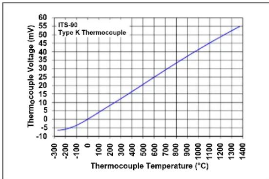
Figure 1 shows the Seebeck voltage as a function of temperature for the standard type K thermocouple. Notice that the response is not strictly linear, but can be linearized over small temperature ranges (e.g., ± 10^ ).
line
| Thermocouple Temperature (°C) | Thermocouple Voltage (mV) | | ----------------------------- | ------------------------- | | -300 | -5 | | -200 | -2 | | -100 | 0 | | 0 | 5 | | 100 | 10 | | 200 | 15 | | 300 | 20 | | 400 | 25 | | 500 | 30 | | 600 | 35 | | 700 | 40 | | 800 | 45 | | 900 | 50 | | 1000 | 55 | | 1100 | 60 | | 1200 | 65 | | 1300 | 70 | | 1400 | 75 |FIGURE 1: Type K Thermocouple's Response.
Most thermocouple junctions behave in a similar manner. The following are examples of thermocouple junctions on a PCB:
- Components soldered to a copper pad
- Wires mechanically attached to the PCB
- Jumpers
- Solder joints
• P C B vi a s
AN1258
The linearized relationship between temperature and thermoelectric voltage, for small temperature ranges, is given in Equation 1. The Seebeck coefficients for the junctions found on PCBs are typically, but not always, below ± 100~ V / ^ .
EQUATION 1: SEEBECK VOLTAGE
$$ \Delta V _ {T H} \quad k _ {J} T _ {J} - (T _ {R E F}) \approx $$
$$ V _ {T H} = V _ {R E F} + \Delta V _ {T H} $$
Where:
$$ \Delta V _ {T H} = \text { Change in Seebeck voltage (V) } $$
$$ k _ {J} = \text { Seebeck coefficient } (V / ^ {\circ} C) $$
$$ T _ {J} = \text { Junction Temperature } (^ {\circ} \mathrm{C}) $$
$$ T _ {R E F} = \text { Reference Temperature } (^ {\circ} \mathrm{C}) $$
$$ V _ {T H} = \text { Seebeck voltage (V) } $$
$$ V _ {R E F} = \text { Seebeck voltage at } T _ {R E F} (\mathrm{V}) $$
Illustrations Using a Resistor
Three different temperature profiles will be shown that illustrate how thermocouple junctions behave on PCB designs. Obviously, many other components will also produce thermoelectric voltages (e.g., PCB edge connectors).
Figure 2 shows a surface mount resistor with two metal (copper) traces on a PCB. The resistor is built with end caps for soldering to the PCB and a very thin conducting film that produces the desired resistance. Thus, there are three conductor types shown in this figure, with four junctions.
| Resistor Film | Copper Traces | Resistor End Caps |
| Junction #1 | Junction #4 |
| Junction #2 | Junction #3 |
FIGURE 2: Resistor and Metal Traces on PCB.
For illustrative purposes, we'll use the arbitrary values shown in Table 1. Notice that junctions 1 and 4 are the same, but the values are shown with opposite polarities; this is one way to account for the direction current flows through these junctions (the same applies to junctions 2 and 3).
TABLE 1: ASSUMED THERMOCOUPLE JUNCTION PARAMETERS
| Junction No. | VREF(mV) | kJ(μV/°C) |
| 1 | 10 | 40 |
| 2 | -4 | -10 |
| 3 | 4 | 10 |
| 4 | -10 | -40 |
Note 1: V_REF and k_J have polarities that assume a left-to-right horizontal direction.
2: T_REF = 25^.
CONSTANT TEMPERATURE
In this illustration, temperature is constant across the PCB. This means that the junctions are at the same temperature. Let's also assume that this temperature is +125°C and that the voltage on the left trace is 0V. The results are shown in Figure 3. Notice that V_TH is the voltage change from one conductor to the next.
$$ 1 4 \mathrm{mV} \quad 9 \mathrm{mV} \quad 1 4 \mathrm{mV} $$
$$ 0 \mathrm{mV} \quad 0 \mathrm{mV} $$
$$ \begin{array}{l l} + 1 2 5. 0 0 ^ {\circ} \mathrm{C} & + 1 2 5. 0 0 ^ {\circ} \mathrm{C} \ + 1 2 5. 0 0 ^ {\circ} \mathrm{C} & + 1 2 5. 0 0 ^ {\circ} \mathrm{C} \end{array} $$
| Location | V_REF (mV) | V_TH (mV) | V_TH (mV) |
| Junction #1 | 10 | 4 | 14 |
| Junction #2 | -4 -1 | -5 | |
| Junction #3 | 4 | 1 | 5 |
| Junction #4 | -10 -4 | -14 |
FIGURE 3: Constant Temperature Results.
TEMPERATURE CHANGE IN THE NORMAL DIRECTION
In this illustration, temperature changes vertically in Figure 2 (normal to the resistor's axial direction), but does not change in the axial direction (horizontally).
The metal areas maintain almost constant voltages in the normal direction, so this case is basically the same as the previous one.
Note: When temperature is constant along the direction of current flow, the net change in thermoelectric voltage between two conductors of the same material is zero.
TEMPERATURE CHANGE IN THE AXIAL DIRECTION
In this illustration, temperature changes horizontally in Figure 2 (along the resistor's axial direction), but does not change in the normal direction (vertically). Let's assume 0V on the left copper trace, +125°C at Junction #1, a temperature gradient of 10°C/in (0.394°C/mm) from left to right (0 in the vertical direction) and a 1206 SMD resistor.
The resistor is 0.12 inches long (3.05 mm) and 0.06 inches wide (1.52 mm). Assume the end caps are about 0.01 inches long (0.25 mm) and the metal film is about 0.10 inches long (2.54 mm). The results are shown in Figure 4.

other
| Location | V_REF (mV) | ΔV_TH (mV) | V_TH (mV) | |---|---|---|---| | Junction #1 | 10 4.00 | 0 14.00 | 0 | | Junction #2 | -4 -1.00 | 1 -5.00 | 1 | | Junction #3 | 4 | 1.011 | 5.011 | | Junction #4 | -10 | -4.048 | -14.048 |FIGURE 4: Axial Gradient Results.
Thus, the temperature gradient of 10^ C/in ( 1.2^ C increase from left to right) caused a total of -38 V to appear across this resistor. Notice that adding the same temperature change to all junction temperatures will not change this result.
Note: Shifting all of the junction temperatures by the same amount does not change the temperature gradient. This means that the voltage drop between any two points in the circuit using the same conductive material is the same (assuming we're within the linear region of response).
PREVENTING LARGE THERMOELECTRIC VOLTAGES
This section includes several general techniques that prevent the appearance of large temperature gradients at critical components.
Reduced Heat Generation
When a PCB's thermal gradient is mainly caused by components attached to it, then find components that dissipate less power. This can be easy to do (e.g., change resistors) or hard (change a PICmicro® microcontroller).
Increasing the load resistance, and other resistor values, also reduces the dissipated power. Choose lower power supply voltages, where possible, to further reduce the dissipated power.
Redirect the Heat Flow
Changing the direction that heat flows on a PCB, or in its immediate environment, can significantly reduce temperature gradients. The goal is to create nearly constant temperatures in critical areas.
ALTERNATE HEAT PATHS
Adding heat sinks to parts that dissipate a lot of power will redirect the heat to the surrounding air. One form of heat sink that is often overlooked is either ground planes or power planes in the PCB; they have the advantage of making temperature gradients on a PCB lower because of their large (horizontal) thermal conductivity.
Adding a fan to a design will also redirect heat to the surrounding air, which reduces the temperature drop on the PCB. This approach, however, is usually avoided to minimize other design issues (random temperature fluctuations, acoustic noise, power, cost, etc.). It is important to minimize air (convection) currents near critical components. Enclose either the parts with significant temperature rise, or the critical parts. Conformal coating may also help.
ISOLATION FROM HEAT GENERATORS
It is possible to thermally isolate critical areas on the PCB. Regions with little or no metal act like a good thermal insulator. Signals that need to cross these regions can be sent through series resistors, which will also act as poorly conducting thermal elements.
Place heat sources as far away from critical points as possible. Since many heat sources are in the external environment, it can be important to place these critical points far away from the edges of the PCB. Components that dissipate a lot of power should be kept far away from critical areas of the PCB.
Low profile components will have reduced exposure to the external environment. They may have the additional advantage of reduced electrical crosstalk.
Thermal barriers, such and conformal coating and PCB enclosures, can be helpful too. They usually do not have to be added unless there are other compelling reasons to do so.
Slow Temperature Changes
In some applications, sudden changes in thermoelectric voltages can also be a concern.
Avoid power-up and power-down thermal transient problems by minimizing the currents drawn during these times. Also, reducing the times can help.
Quick changes in voltages at heavy loads can be another source of concern. If the load cannot be made lighter, then isolation is usually the best approach to solving this problem.
CURING THERMOELECTRIC VOLTAGE EFFECTS
This section focuses on methods that minimize the effects of a given temperature gradient. They can be powerful aids in improving a design because they tend to be low cost.
Metallurgy
Critical points, that need to have the same total thermoelectric voltage, should use the same conductive material. For example, the inputs to an op amp should connect to the same materials. The PCB traces will match well, but components with different constructions may be a source of trouble.
It is possible to find combinations of metals and solders that have low Seebeck coefficients. While this obviously reduces voltage errors, this can be complicated and expensive to implement in manufacturing.
Following Contour Lines
Place critical components so that their current flow follows constant temperature contour lines; this minimizes their thermoelectric voltages. Figure 5 shows an inverting amplifier that will be used to illustrate this concept; R_N , R_G and R_F are the critical components in this circuit.

text_image
V_IN R_G R_F V_OUT R_N - + U_1 C_1 V_DDFIGURE 5: Inverting Amplifier.
Figure 6 shows one implementation of this concept. Constant temperature contour lines become reasonably straight when they are far from the heat source. Placing the resistors in parallel with these lines minimizes the temperature drop across them.

text_image
Heat Source Constant Temperature Contour Lines VIN RF U1 VDD RG RN C1 VOUTFIGURE 6: Resistors Aligned with Contour Lines.
The main drawback to this technique is that the contour lines change when the external thermal environment changes. For instance, picking up a PCB with your hands adds heat to the PCB, usually at locations not accounted for in the design.
Cancellation of Thermoelectric Voltages
It is possible to cancel thermoelectric voltages when the temperature gradient is constant. Several examples will be given to make this technique easy to understand.
TRADITIONAL OP AMP LAYOUT APPROACH
Figure 7 shows a non-inverting amplifier that needs to have the resistors' thermoelectric voltage effect minimized. The traditional approach is to lay out the input resistors ( R_N and R_G ) close together, at equal distances from the op amp input pins and in parallel.

text_image
V_IN R_N U_1 + - C_1 V_DD R_G R_F V_OUTFIGURE 7: Non-inverting Amplifier.
Figure 8 shows one layout that follows the traditional approach, together with a circuit diagram that includes the resulting thermoelectric voltages ( V_THx and V_THy ). V_THx is positive on the right side of a horizontally oriented component (e.g., R_N ). V_THy is positive on the top side of a vertically oriented component (e.g., R_F ).

text_image
RF RG RN VIN U1 VDD C1 VOUT C1 VIN RN VTHx + - + - Rg VTHx RF VTHy VOUTFIGURE 8: One Possible Layout (not recommended) and its Thermoelectric Voltage Model.
The output has a simple relationship to the inputs ( V_IN and the three V_THx and V_THy sources):
EQUATION 2:
$$ \begin{array}{l} G _ {N} \quad 1 R _ {F} / + R _ {G} \ V _ {O U T} = V _ {I N} + \left(V _ {T H x} \quad_ {N} Y _ {T H x} G _ {N} \quad \mathbf {G} (+ T H y) \right. \ = V _ {I N} G _ {N} + V _ {T H x} + V _ {T H y} \ \end{array} $$
When the gain (G_N) is high, the thermoelectric voltage contributes little to the output error. This layout may be good enough in that case. Notice that the cancellation between R_N and R_G is critical to good performance.
When the gain is low, or the very best performance is desired, this layout needs improvement. The following sections give guidance that helps achieve this goal.
SINGLE RESISTOR SUBSTITUTIONS
A single resistor on a PCB will produce a thermoelectric voltage, as discussed before. Replacing that resistor with two resistors that are properly aligned will cancel the two resulting thermoelectric voltages.
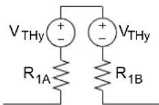
Figure 9 shows the original resistor and its model on the top, and a two series resistor substitution and its model on the bottom.
The original resistor has a thermally induced voltage V_THx that is based on the temperature gradient in the x-direction (horizontal).
The two resistors on the bottom have thermally induced voltages V_THy that are based on the temperature gradient in the y-direction (vertical); they are equal because the temperature gradient is constant and the resistor lengths are equal. Due to their parallel alignment, these voltages cancel; the net thermally induced voltage for this combination (as laid out) is zero.

Where:
$$ R _ {1 A} = R _ {1 B} = R _ {1} / 2 $$
FIGURE 9: Series Resistor Substitution.
Note: The orientation of these two resistors (R 1A and R 1B ) is critical to canceling the thermoelectric voltages.
Figure 10 shows the original resistor and its model on the top, and a two parallel resistor substitution and its model on the bottom.
The original resistor has a thermally induced voltage V_THx that is based on the temperature gradient in the x-direction (horizontal).
The two resistors on the bottom have thermally induced voltages V_THy that are based on the temperature gradient in the y-direction (vertical); they are equal because the temperature gradient is constant and the resistor lengths are equal. Due to their orientation, and because R_1A = R_1B , these voltages produce currents that cancel. The net thermally induced voltage for this combination (as laid out) is zero.

text_image
R1 R1A R1B VTHx R1 VTHy + - R1B R1A VTHy Where: R1A = R1B = 2R1FIGURE 10: Parallel Resistor Substitution.
NON-INVERTING AMPLIFIER
Figure 11 shows a non-inverting amplifier. We will start with the layout in Figure 12 (previously shown in Figure 6). The resistor R_F is horizontal so that all of the thermoelectric voltages may be (hopefully) cancelled. The model shows how the thermoelectric voltages modify the circuit.
text_image
V_IN R_N U_1 C_1 V_DD R_G R_F V_OUTFIGURE 11: Non-inverting Amplifier.
text_image
RF RG RN VIN U1 VDD C1 VOUT VDD C1 VIN RN VTHx + - U1 RG VTHx + - RF VTHx VOUTFIGURE 12: First Layout (not recommended) and its Thermoelectric Voltage Model.
The output has a simple relationship to the inputs ( V_IN and the three V_THx sources):
EQUATION 3:
$$ \begin{array}{l} G _ {N} \quad 1 R _ {F} / + R _ {G} \ V _ {O U T} = V _ {I N} + \left(V _ {T H x} - Y _ {T H x} \left(G _ {N} - 1\right) + V _ {T H x} \right. \ = V _ {I N} G _ {N} + 2 V _ {T H x} \ \end{array} $$
When the gain ( G_N ) is high, the thermoelectric voltage's contribution to the output error is relatively small. This layout may be good enough in that case. Notice that the cancellation between R_N and R_G is critical.
We have a better layout shown in Figure 13. Recognizing that subtracting the last term in the V_OUT equation (middle equation in Equation 3) completely cancels the thermoelectric voltages, the resistor R_F was oriented in the reverse direction.

text_image
RF U1 VDD RG RN C1 VIN VOUT VDD C1 VIN R_N V_DD U1 R_G V_THx RF V_THx VOUTFIGURE 13: Second Layout and its Thermoelectric Voltage Model.
With the reversed direction for R_F , the output voltage is now:
EQUATION 4:
$$ G _ {N} \quad 1 R _ {F} / R _ {G} $$
$$ V _ {O U T} = V _ {I N} + \left(V _ {T H x} \quad_ {N} \quad \forall_ {T H x} G _ {N} \quad 1 G (\quad_ {T H x}) \right. $$
$$ \nleq_ {I N} G _ {N} $$
The cancellation between R_N and R_G is critical to this layout; the change to R_F 's position is not as important.
INVERTING AMPLIFIER
Inverting amplifiers use the same components as non-inverting amplifiers, so the resistor layout is the same; see Figure 14.
text_image
VIN RF U1 VDD RG RN C1 VOUT VIN RG RF VOUT RN - U1 C1 VDDFIGURE 14: Inverting Amplifier.
DIFFERENCE AMPLIFIER
Figure 15 shows a difference amplifier. This topology has an inherent symmetry between the non-inverting and inverting signal paths, which lends itself to cancelling the thermoelectric voltages. Figure 16 shows the layout and its model.

text_image
+ VIN - RG RF U1 + - C1 VDD VREF RG RF VOUTFIGURE 15: Difference Amplifier.
text_image
- VIN + RF U1 RG RG RF VREF VOUT VDD C1 + VIN - RG VTHx RF VTHx - + - + VDD C1 + U1 - RG VTHx RF VTHx - + - + VREF VOUTFIGURE 16: Difference Amplifier Layout and its Thermoelectric Voltage Model.
The output has a simple relationship to the inputs ( V_IN , V_REF and the four V_THX sources):
EQUATION 5:
$$ \begin{array}{l} G = R _ {F} / R _ {G} \ V _ {O U T} = \left(V _ {I N} + V _ {T H x} - V _ {T H x}\right) G \ + \left(V _ {R E F} + V _ {T H x} - V _ {T H x}\right) \ V \leq_ {I N} G + V _ {R E F} \ \end{array} $$
INSTRUMENTATION AMPLIFIER INPUT STAGE
Figure 17 shows an instrumentation amplifier input stage, which is sometimes used to drive the input of a differential ADC. While this is a symmetrical circuit, achieving good thermoelectric voltage cancellation on the PCB presents difficulties. It is best to use a dual op amp, so the R_F resistors have to be on both sides of the op amp, while R_G connects both sides; the distances between resistors are too large to be practical (thermal gradient is not constant).

text_image
U1A VDD + - C1 + VIN RG RF VOUT - R_N R_F R_N U1BFIGURE 17: Instrumentation Amplifier Input Stage (not recommended).
The solution to this problem is very simple; split R_G into two equal series resistors so that we can use the non-inverting layout (see Figure 13) on both sides of the dual op amp. Each side of this amplifier will cancel its thermoelectric voltages independently; this is shown in Figure 18 and Figure 19.
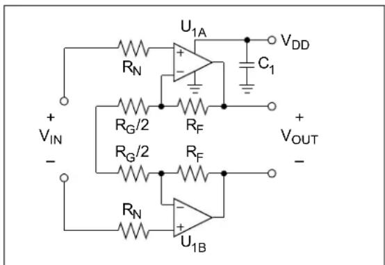
text_image
U1A RN + - C1 VDD + VIN RG/2 RF RG/2 RF - VOUT - RN + - U1BFIGURE 18: Instrumentation Amplifier Input Stage.

text_image
C1 RF U1 RF RG/2 RN RG/2 VIN- VOUT+ VDD VOUT- VIN+ VOUT- VDD C1 VDD U1A RN VTHx + - + - + - + - Rg/2 VTHx RF VTHx + - + - + - + - Rg/2 VTHx RF VTHx - + - + - Rg/2 VTHx U1B - + - + - + - + - + - + - + - + - + - + - + - + - + - + - + - + - + - + - + - + - + - + - + - + - + - + - + - + - + - + - + - + - + - + - + - + - + - + - + - + - + - + - + - + - + - + - + - + - + - + - + - + - + VIN - VOUTFIGURE 19: Instrumentation Amplifier Input Stage Layout and its Thermoelectric Voltage Model.
The V_THx sources cancel, for the reasons already given, so the differential output voltage is simply:
EQUATION 6:
$$ G 1 \quad 2 \quad R _ {F} / R _ {G} $$
$$ V _ {O U T} \quad V _ {I N} G = $$
MODIFICATIONS FOR NON-CONSTANT TEMPERATURE GRADIENTS
Temperature gradients are never exactly constant. One cause is the wide range of thermal conductivities (e.g., traces vs. FR4) on a PCB, which causes complex temperature profiles. Another cause is that many heat sources act like point sources, and the heat is mainly conducted by a two dimensional object (the PCB); the temperature changes rapidly near the source and slower far away.
Non-constant temperature gradients will cause the temperature profile to have significant curvature, which causes all of the previous techniques to have less than perfect success. Usually, the curvature is small enough so that those techniques are still worth using. Sometimes, additional measures are needed to overcome the problems caused by the curvature.
One method is to minimize the size of critical components (e.g., resistors). If we assume that temperature has a quadratic shape, then using components that are half as long should reduce the non-linearity error to about one quarter the size.
Another method is to keep all heat sources and sinks far away from the critical components. This makes the contour lines straighter.
The contour lines can be deliberately changed in shape. Using a ground plane (also power planes) to conduct heat away from the sources helps equalize the temperatures, which reduces the non-linear errors. Adding guard traces or thermal heat sinks that surround the critical components also help equalize the temperatures.
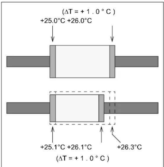
We can modify the sizes of the critical components so that the cancellation becomes closer to exact. In order to match resistors, for instance, we need to make sure that the temperature change across each of the matched resistors is equal; see Figure 20 for an illustration.
text_image
(ΔT = + 1 . 0 °C) +25.0°C +26.0°C +25.1°C +26.1°C +26.3°C (ΔT = + 1 . 0 °C)FIGURE 20: Example of Mismatching the Component Sizes.
MEASUREMENT OF TEMPERATURE RELATED QUANTITIES
While the techniques previously shown are a great help in producing an initial PCB layout, it is important to verify that your design functions as specified. This section includes methods for measuring the response of individual components and of a PCB. With this information, it is possible to make intelligent design tweaks.
TEMPERATURE
There are many ways to measure temperature [4, 5, 6]. We could use thermocouples, RTDs, thermistors, diodes, ICs or thermal imagers (infrared cameras) to measure the temperature.
Figure 21 shows a circuit based on the MCP9700 IC temperature sensor. Because all of the components draw very little current, their effect on PCB temperature will be minimal. There is enough filtering and gain to make V_OUT easy to interpret. This circuit can be built on a very small board of its own, which can be easily placed on top of the PCB of interest.

text_image
VDD = 5.0 V U1 100 nF C1 1.0 μF MCP9700 Temp. 100 kΩ Sensor TPCB VDD C4 100 nF U2 MCP6041 R2 113 kΩ R3 12.4 kΩ R4 100 kΩ R5 1.00 MΩ R6 VOUT C2 1.0 μF C3 22 nFFIGURE 21: IC Temperature Sensor Circuit.
The MCP9700 outputs a voltage of about 500 mV plus 10.0 mV/°C times the board temperature ( T_PCB , in °C). The amplifier provides a gain of 10 V/V centered on 500 mV (when V_DD = 5.0V ), giving:
EQUATION 7:
$$ V _ {O U T} = (5 0 0 \mathrm{mV}) + T _ {P C B} (1 0 0 \mathrm {mV / ^ {\circ} C}) $$
Since the MCP9700 outputs a voltage proportional to temperature, V_OUT needs to be sampled by an ADC that uses an absolute voltage reference.
The absolute accuracy of this circuit does not support our application, so it is important to calibrate the errors. Leave the PCB in a powered-off state (except for the temperature sensor) for several minutes. Measure V_OUT at each point, with adequate averaging. The changes in V_OUT from the calibration value represents the change in T_PCB from the no power condition.
THERMAL GRADIENTS
To measure thermal gradients, simply measure the temperature at several points on the PCB. The gradient is then the change in temperature divided by the distance between points. More points give better resolution on the gradient, but reduce the accuracy of the numerical derivative.
PACKAGE THERMAL RESISTANCE
The way to estimate the temperature (T in °C) of a component is to multiply its dissipated power (P in W) by the package thermal resistance ( _JA in °C/W). This helps establish temperature maximum points.
To measure _JA , when it is not given in a data sheet, place the temperature sensor at the IC (usually, a thermocouple between the package and the PCB). Insert a small resistor in the supply to measure the supply current when on ( I_DD in A). Measure the change in temperature ( T in ^ ) between the off and on conditions, supply voltage ( V_DD in V) and I_DD . Then,
EQUATION 8:
$$ \theta_ {J A} \quad \frac {\Delta T}{V _ {D D} I _ {D D}} = $$
THERMOELECTRIC VOLTAGES
The easiest way to measure thermoelectric voltages is to thermally imbalance a difference amplifier circuit. The thermoelectric voltages have a polarity that adds (instead of cancelling) in Figure 22 (compare to Figure 16). The differential input voltage is zero, and the resistors are larger to emphasize the thermoelectric voltages.
The large resistor on the right of the layout can be used to generate heat, causing a horizontal temperature gradient at the resistors R_G and R_F . The gain (G) is set high to make the measurements more accurate. The thermoelectric voltage ( V_THx ) across one resistor is:
EQUATION 9:
$$ \begin{array}{r l} {G} & {R _ {F} / \mathbb {R} _ {G}} \ {V _ {T H x}} & {\frac {V _ {O U T} - V _ {R E F}}{2 G 2 +} =} \end{array} $$
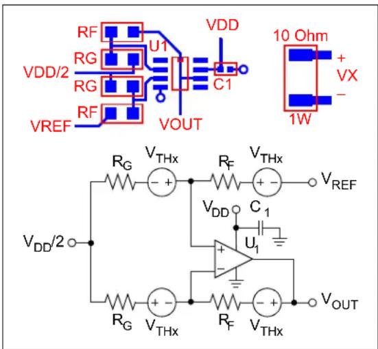
text_image
VDD 10 Ohm + VX - 1W VREF RF RG U1 C1 VDD/2 RG VOUT R_G V_THx R_F V_THx V_REF V_DD/2 R_G V_THx R_F V_THx V_DD C_1 U_1 V_OUTFIGURE 22: Difference Amplifier with Deliberately Unbalanced Thermoelectric Voltages and Heat Generating Resistor.
We can also place a short across one component, of a matched pair, with a copper trace on the PCB. Figure 23 shows a non-inverting amplifier layout that shorts R_N (with a copper trace) to unbalance the thermoelectric voltages. It also connects the two inputs together, and uses larger resistors, to simplify measurements ( V_OUT = V_DD/2 , ideally). The short is easily removed from the PCB.
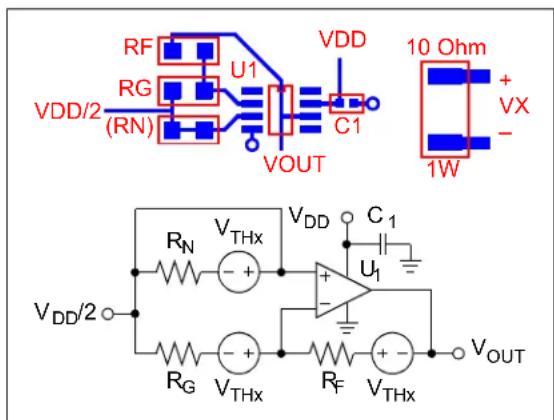
text_image
VDD/2 RF RG (RN) U1 VOUT VDD C1 10 Ohm + VX - 1W RN VTHx VDD C1 U1 VDD/2 RG VTHx Rf VTHx VOUTFIGURE 23: Shorted Resistor (R _N ) that Unbalances Thermoelectric Voltages.
With the unbalance, we now have the thermoelectric voltage:
EQUATION 10:
$$ \begin{array}{r l} {G _ {N}} & {1 R + _ {F} / = R _ {G}} \ {V _ {T H x} =} & {\frac {V _ {O U T} V _ {D D} 2 / -}{- G _ {N}}} \end{array} $$
TROUBLESHOOTING TIPS AND TRICKS
Using a strip chart to track the change in critical DC voltages over time helps locate the physical source of the errors. Not only can it show how large the change is between two different thermal conditions (e.g., on and off), but it shows the time constants of these shifts. They can be roughly divided into the following three categories:
- Time constant << 1 s, within component (e.g., thermal crosstalk within an op amp)
- Time constant ≈ 1 s, single component (e.g., in an eight lead SOIC package)
• Time constant >> 1 s, PCB and its environment
To quickly and easily change the temperature at one location on a PCB, do the following. Use a clean drinking straw to blow air at the location (component) of interest. Use a piece of paper to re-direct the airflow away from other nearby components. When troubleshooting, the paper can be used to divide a PCB area in half to help locate the problem component. This approach does not give exact numbers, but can be used to quickly find problem components on a PCB.
You can use a heat sink (with electrically insulating heat sink compound) to reduce the temperature difference between two critical points on your PCB. The greater the area covered at both ends of the heat sink, the quicker and better this thermal "short" will work.
LEAKAGE CURRENTS
Leakage currents cause voltage drops when they flow through either resistors or parasitic resistances. This section focuses on parasitic resistances presented by the PCB: surface resistance and bulk (through the dielectric) resistance.
Leakage currents cause voltage ramps when they flow into a capacitor. Common examples are the gain capacitor of a transimpedance amplifier (see Figure 32) and the non-inverting input of an op amp with no DC path to ground (not recommended).
Op amp leakage (bias) currents are discussed in [2].
High Impedance Sources
High impedance signal sources are susceptible to errors caused by leakage currents. These sources are usually modeled as a current source with a high parallel resistance (a Norton model):
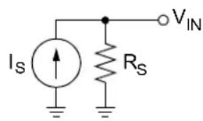
FIGURE 24: Norton Source Model.
One sensor that is modeled as a Norton current source is the photodiode [1]. A common op amp circuit used for photocurrent measurements is the transimpedance amplifier (see Figure 32).
Sometimes, high impedance sources are modeled as a voltage source with a high series resistance (a Thevenin model):

FIGURE 25: Thevenin Source Model.
The pH electrode [1] is one example with a Thevenin source. A common op amp implementation is a non-inverting amplifier.
PCB Surface Leakage
PARASITIC SURFACE RESISTANCES
Surface contamination on a PCB creates resistive paths for leakage currents. These leakage currents can cause appreciable voltage shifts, even in well-designed circuits. The contamination can be humidity (moisture), dust, chemical residue, etc.
On a PCB, leakage currents flow on the surface, to a sensitive node (high resistance), from nearby bare metal objects (including traces) at a different voltage.
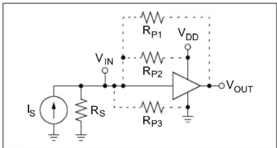
To model sensitivity to surface contamination in your circuit, add resistors between the high impedance node and other nearby nodes. For example, Figure 26 shows an amplifier circuit with a Thevenin source ( V_S and R_S ). Since R_S is high and the amplifier's input is high impedance, V_IN is a high impedance node. Parasitic resistances ( R_P1 to R_P4 ) are connected to all other (nearby) voltage nodes (traces on a PCB), including ground. R_P1 to R_P4 are open-circuited for most design work. For leakage current design calculations, they take on high resistance values (usually one at a time).

text_image
V_IN R_P1 V_DD R_P2 R_P3 V_OUT R_S R_P4 V_SFIGURE 26: Thevenin Source and Parasitic Leakage Resistances.
Figure 27 shows an amplifier circuit with a Norton source.
text_image
Is RS VIN RP1 VDD RP2 RP3 VOUTFIGURE 27: Norton Source and Parasitic Leakage Resistances.
The parasitic resistor values ( R_p ) depend on your PCB layout. For a typical layout, with today's geometries (traces are close and short) and materials, we have:
- R_P 1000G , low humidity and contamination
- R_P 1 G , high humidity and contamination
These R_P values need to be modified for atypical geometries; see Appendix B: “PCB Parasitic Resistance”. These R_P values also need to be modified for the worst case conditions for your application. Measurements in your conditions, and with your PCB layout, will give better estimates of R_P .
CLEANING
A standard PCB clean step helps minimize surface contamination, but may not eliminate the problem. An additional cleaning step, using isopropyl alcohol, is needed to clean the residue left by some PCB cleaning solvents. This can then be blown dry using compressed air (with an in-line moisture trap).
COATING
In order to maintain the PCB cleanliness after the initial clean, you may coat the PCB surface. The coating needs to be a barrier to moisture and other contaminants; solder mask, epoxy and silicone rubber are examples.
The coating will have internal (bulk) leakage currents; this effect needs to be evaluated for your design.
GUARD RINGS
Guard rings surrounding critical signal traces, when properly applied, can significantly reduce PCB surface leakage currents into critical (high resistance) nodes.
These guard rings have no solder mask so that the leakage currents flow into them, instead of into the sensitive trace. The guard ring is biased at the same voltage as the sensitive node; it needs to be driven by a low impedance source.
Guard rings increase the capacitance at critical nodes. Since they are driven by low impedance sources, these capacitances have little effect on performance.
Unity Gain Buffer
Figure 28 shows a unity gain buffer with a guard ring. This guard ring is biased by V_OUT and protects (surrounds) the op amp's non-inverting input (and all top metal connected to it) on the PCB surface. The diagram is for surface mount components only. R_N is an 0805 SMD to give sufficient clearance for the guard ring trace between its pads.
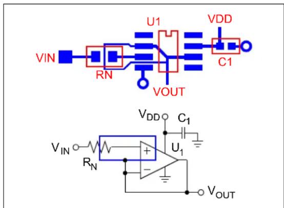
text_image
VIN RN U1 VDD C1 VOUT VDD C1 VIN RN U1 VOUTFIGURE 28: Unity Gain Buffer with Guard Ring.
The parasitic resistances are connected as shown in Figure 29. R_P2 injects current into U_1 's non-inverting input (the high impedance node). The other parasitic resistors inject current into the guard ring, which is driven by V_OUT ; they do not affect the performance.
The voltage across R_P2 is U_1 's offset voltage ( V_OS ), so the leakage current is greatly reduced. For instance, if V_OS ≤ ±2 mV and the voltage without the guard ring is 2V, the leakage current would be reduced by a factor of about 1000.

text_image
V_IN R_P1 R_N R_P2 R_P3 V_DD U_1 C_1 V_OUTFIGURE 29: Equivalent Circuit for Unity Gain Buffer with Guard Ring.
One example of an application that sometimes uses unity gain op amps are pH meters. In that case, however, both V_IN and R_N are located off the PCB; the guard ring only needs to surround U_1 's non-inverting input.
Non-inverting Gain Amplifier
Figure 30 shows a non-inverting gain amplifier with a guard ring. This guard ring is biased by V_OUT , R_F and R_G ; it protects (surrounds) the op amp's non-inverting input (and all top metal connected to it) on the PCB surface. R_F and R_G are low impedance, to drive the guard ring properly. R_N is a low valued resistor that cancels thermojunction voltage effects, but has little effect on bias current errors (e.g., I_BR_N << ± 1 mV ).
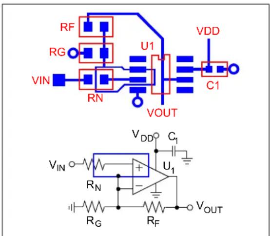
text_image
RF RG VIN RN U1 VDD C1 VOUT VDD C1 VIN RN U1 VOUT RG RFFIGURE 30: Non-inverting Gain Amplifier with Guard Ring.
The parasitic resistances are connected as shown in Figure 31. Similar to the Unity Gain Buffer in the last section, U_1 's offset voltage ( V_OS ) is across R_P2 , which greatly reduces its leakage current. The other parasitic resistances are driven by V_OUT , R_F and R_G ; they do not affect the performance. The leakage current is typically reduced by a factor of about 1000.
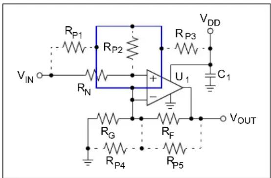
text_image
V_IN R_P1 R_N R_P2 U_1 R_P3 V_DD C_1 R_G R_F V_OUT R_P4 R_P5FIGURE 31: Equivalent Circuit for Non-inverting Amplifier with Guard Ring.
Transimpedance Amplifier
Figure 32 shows a photo-diode at the input of a transimpedance amplifier, with a guard ring. This guard ring is biased at ground; it protects (surrounds) the op amp's inverting input (and all top metal connected to it) on the PCB surface. R_F is high valued for the DC gain ( V_OUT/I_D1 ).
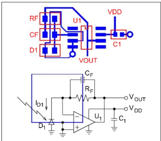
text_image
RF CF D1 U1 VOUT VDD C1 CF RF ID1 D1 U1 VOUT VDD C1FIGURE 32: Photo-diode and Transimpedance Amplifier, with Guard Ring.
The parasitic resistances are connected as shown in Figure 33. Similar to the Non-inverting Gain Amplifier in the last section, U_1 's offset voltage ( V_OS ) is across R_P1 , which greatly reduces its leakage current. The other parasitic resistances are connected to ground; they do not affect the performance. The leakage current is typically reduced by a factor of about 1000.

text_image
R_{P1} I_{D1} D_1 C_F R_F U_1 R_{P3} C_1 V_{OUT} V_{DD}FIGURE 33: Equivalent Circuit for Photo-diode and Transimpedance Amplifier, with Guard Ring.
Guard Rings on Both PCB Surfaces
For op amps in through-hole packages (e.g., PDIP), guard rings are needed on both top and bottom surfaces. The same design principles apply to both surfaces.
Any jumper traces (via to other surface, trace and via back to the original surface), connected to traces with guard rings, also need guard rings around the jumper traces. It is better, when possible, to avoid jumper traces for critical nodes.
PCB Bulk Leakage
The dielectric material used in a PCB (e.g., FR4) is an insulator. Its resistance to leakage currents through the bulk (the dielectric) is described by its volume resistivity ( _V ). _V values vary considerably, depending on the dielectric and on ambient conditions.
Usually, bulk leakage currents are much smaller than surface leakage currents; they can be neglected in many designs. Designs that minimize surface leakage currents, however, may be affected by bulk currents.
Example 1 shows one example of how bulk leakage currents occur. Two traces run in parallel and are separated by the dielectric. The leakage current between the traces, flowing through the dielectric, is modelled by a parasitic resistor (see R_P1 in Figure 34).
EXAMPLE 1: PARALLEL TRACES, OPPOSITE SURFACES
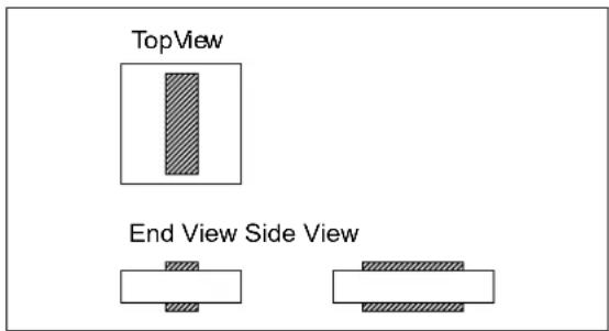
text_image
TopView End View Side View
text_image
Top Trace RP1 Bottom TraceFIGURE 34: Equivalent Circuit for Parallel Traces, Opposite Surfaces.
Any two metal areas on the PCB (on a surface or buried in an inner layer), at different potentials, will have a leakage current between them. The value of the parasitic (bulk) resistance depends on:
• The geometry of the areas
- The distance between
- The cross sectional area seen by the current
- Nearby metal objects (e.g., a guard ring) that modify the current flow path
• The volume resistivity (ρ v)
- Dielectric material
- Exposure to chemicals (e.g., water)
The following discussion shows simple techniques to minimize these leakage currents. See Appendix B: "PCB Parasitic Resistance" for ways to estimate bulk leakage currents.
SEPARATION
Moving traces to the surfaces, from inner layers, increases the distance between them (e.g., Example 1).
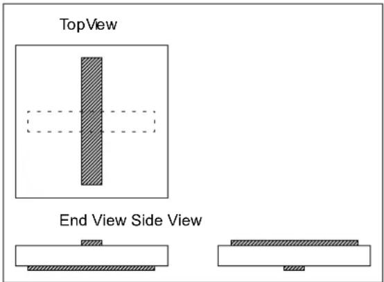
Example 2 shows two parallel traces, with a distance separating them. This extra distance increases the parasitic resistance.
EXAMPLE 2: TWO PARALLEL TRACES, WITH OFFSET

text_image
TopView End View Side ViewCROSSED TRACES
When two traces must cross, place them on opposite surfaces and in normal directions to minimize the parasitic resistance; see Example 3.
EXAMPLE 3: TWO NORMAL TRACES
text_image
TopView End View Side ViewGUARD RINGS
Example 4 shows a trace on the left (node 1), a guard ring (node 2) and a sensitive trace (node 3). The guard ring provides a low resistance path that redirects some of the current between node 1 and node 3 to itself. R_PB2 in Figure 35 acts as an attenuator to the input voltage ( V_1 ). When V_2 ≈ 3 the parasitic current (into V_3 ) is significantly reduced.
EXAMPLE 4: TWO PARALLEL TRACES, WITH GUARD RING

text_image
TopView End View Side View
chemical
Electrical circuit diagram with resistors R_PB1, R_PB2, R_PB3 and voltage nodes V1, V2 (guard ring)FIGURE 35: Equivalent Circuit for Two Parallel Traces, With Guard Ring.
GUARD PLANE
Example 5 shows a trace on the left (node 1), a guard plane (node 2) and a sensitive trace (node 3). The guard plane behaves similar to a guard ring, except that it forms a distributed attenuator to the input voltage (see Figure 36); this attenuation can be much greater.
EXAMPLE 5: TWO PARALLEL TRACES, WITH GUARD PLANE
text_image
TopView End View Side View
text_image
V₁ ○─Rₚᵦ₁─Rₚᵦ₃─Rₚᵦ₅─Rₚᵦ₇─○ V₃ │ │ │ Rₚᵦ₂─Rₚᵦ₄─Rₚᵦ₆─Rₚᵦ₈─○ │ │ └───●─○ │ │ └───●─○ │ │ V₂ (guard plane)FIGURE 36: (Lumped) Equivalent Circuit for Two Parallel Traces, With Guard Plane.
DIELECTRIC MATERIAL
Changing the dielectric material changes its bulk resistivity ( _V ) and susceptibility to humidity. For designs that need exceptional performance, this is an option worth exploring.
MOISTURE CONTROL
When a dielectric is exposed to moisture for an extended period of time, it can become wet. This reduces its bulk resistivity ( _V ).
Measures to control exposure to moisture reduce this effect. One possibility is the use of coatings.
ISOLATING SENSITIVE NODES
Another way to minimize PCB leakage currents is to isolate sensitive nodes (wires, package pins, etc.) from the board (i.e., not touching).
One approach is to use teflon stand-offs. This has technical advantages, but can be costly to implement.
Another approach is to keep sensitive nodes in the air. Bending package leads and routing holes in the PCB are possible techniques to accomplish this.
OTHER TIPS
This section discusses other effects and design tips.
Packages
IC packages contribute to leakage currents. Pins that are close together (fine pitch) will see greater leakage currents, due to dust and shorter leakage paths. The package itself will have bulk leakage, which depends on its chemistry.
Piezoelectric Effect
Some capacitors accumulate extra charge from mechanical stress (a variable capacitor), creating a DC shift. Some ceramic capacitors (not all) suffer from this effect. Minimize stresses with acoustic noise reduction techniques, and by making the PCB assembly more rigid.
Triboelectric Effect
Mechanical friction can cause charges to accumulate (a variable capacitor), causing a DC shift. Air flow over a PCB is one source of mechanical friction. Flexing wires and coax cables excessively can also cause this to happen. Shield against air flow, and make bends in wiring with a large radius. For remote sensors, use low noise coax or triax cable.
Contact Potential
Sometimes, for convenience on the bench, a PCB has sockets for critical components (e.g., an op amp). While these sockets make it easy to change components, they cause significant DC errors in high precision designs.
The problem is that the socket and the IC pins are made of different metals, and are mechanically forced into contact. In this situation, there is a (contact) voltage potential developed between the metals (the Volta effect). Physicists explain this phenomenon through the difference between their work functions. In our bench tests of our auto-zeroed op amps, we saw voltage potentials of ±1 V to ±2 V due to the IC socket.
The solution is very simple; do not use sockets for critical components. Instead, solder all critical components to the PCB.
DESIGN EXAMPLE
This section goes over the thermal design of a thermocouple PCB available from Microchip. This PCB has the following descriptors:
- MCP6V01 Thermocouple Auto-Zeroed Reference Design
• 104-00169-R2 - MCP6V01RD-TCPL
The application of this PCB is discussed in detail in reference [7].
Circuit Description
Figure 37 shows the general functionality of this design (the schematic is shown in Figure A-1).
flowchart
graph TD
    A["PC (Thermal Management Software)"] -->|USB| B["PIC18F2250 (USB) Microcontroller"]
    B --> C["I²CTM Port"]
    B --> D["CVREF"]
    B --> E["10-bit ADC Module"]
    F["MCP1541 4.1V Reference"] -->|VREF| G["2nd Order, Low-pass Filter"]
    G --> H["MCP6V01 Difference Amp."]
    H --> I["Typ K Thermocouple (welded bead)"]
    I --> J["Connector (cold junction)"]
    J --> K["TJC"]
    K --> L["Type K Thermocouple (welded bead)"]
    L --> M["MC9800 Temp. Sensor (cold junction compensation)"]
    M --> N["SDA, SCLK, ALERT"]
    N --> O["×1"]
    O --> P["V_SHIFT"]
    P --> Q["MCP9800 Temp. Sensor (cold junction compensation)"]
    Q --> R["T_CJ"]
    R --> S["Connector (cold junction)"]
    S --> T["VP"]
    S --> U["VM"]
    T --> V["Output"]
    U --> W["Output"]
FIGURE 37: Thermocouple Circuit's Block Diagram.
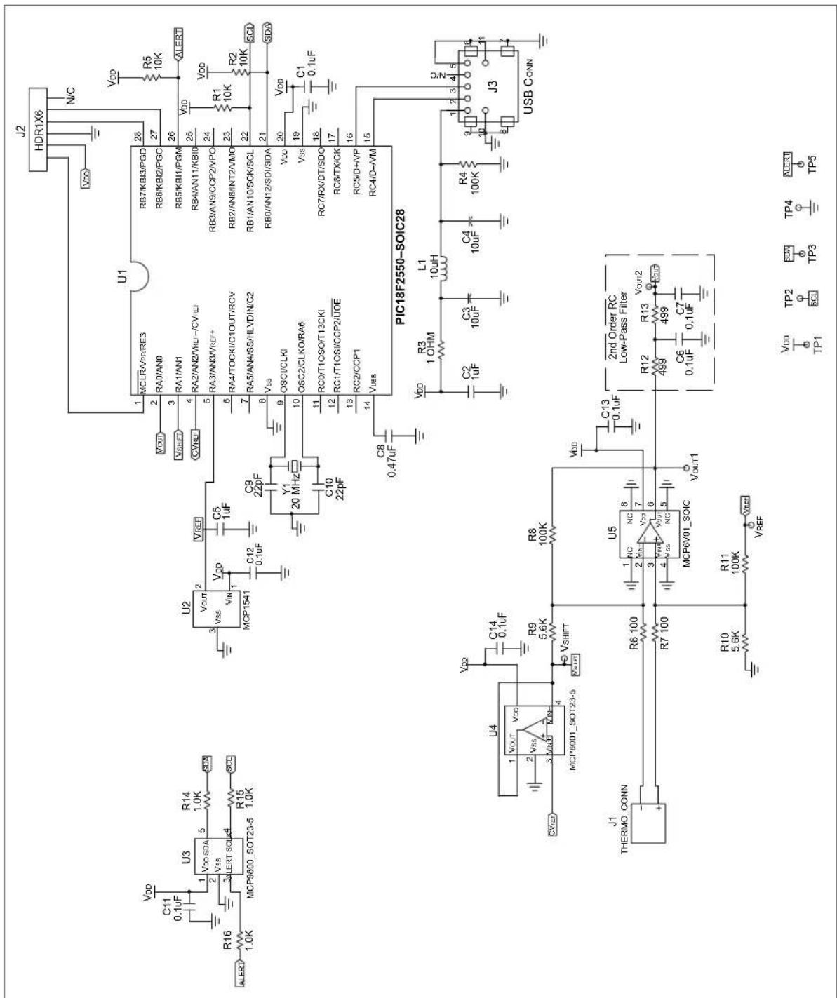
The (type K) thermocouple senses temperature at its hot junction ( T_TC ) and produces a voltage at the cold junction (at temperature T_CJ ). The conversion constant for type K thermocouples is roughly 40 V/^ . This voltage ( V_P-V_M ) is input to the Difference Amplifier (MCP6V01).
The MCP9800 senses temperature at the Type K Thermocouple's cold junction ( T_CJ ). The result is sent to the PICmicro microcontroller via an P_C^TM bus. The firmware corrects the measured temperature for T_CJ .
The difference amplifier uses the MCP6V01 auto-zeroed op amp to amplify the thermocouple's output voltage. The V_REF input shifts the output voltage down so that the temperature range includes -100^ . The V_SHIFT input shifts the output voltage, using a
digital POT internal to the microcontroller (CVREF), so that the temperature range is segmented into 16 smaller ranges; this gives a greater range (-100°C to +1000°C) with reasonable accuracy.
The MCP1541 provides an absolute reference voltage because the thermocouple's voltage depends only on temperature (not on V_DD ). It sets the nominal V_OUT and serves as the reference for the ADC internal to the microcontroller.
The 2^nd Order, Low-pass Filter reduces noise and aliasing at the ADC input. A double R-C filter was chosen to minimize DC errors and complexity.
CVREF is a digital POT with low accuracy and highly variable output resistance. The buffer ( ×1 amplifier) eliminates the output impedance problem, producing the voltage V_SHIFT . Since CVREF has 16 levels, we can shift V_OUT1 by 16 different amounts, creating 16 smaller ranges; this adds 4 bits resolution to the measured results (the most significant bits). The 10 bits produced by the ADC are the least significant bits; they describe the measured values within one of the 16 different smaller ranges.
V_SHIFT is brought back into the PICmicro microcontroller so that it can be sampled by the ADC. This gives V_SHIFT values the same accuracy as the ADC (“10 bits”), which is significantly better than CVREF’s accuracy. The measured value of V_OUT2 is adjusted by this measured V_SHIFT value.
The overall accuracy of this mixed signal solution is set by the 10-bit ADC. The resolution is 14 bits, but the accuracy cannot be better than the ADC, since it calibrates the measurements.
PCB Layout
In the figures in this section (Figure 38 through Figure 43), the red numbers (inside the circles) point to key design choices, which are described by a list after each figure.
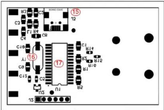
Figure 38 shows the top silk screen layer of the PCB designed for the MCP6V01 Thermocouple Auto-Zeroed Reference Design.
text_image
MCP6V01 Thermocouple Auto-Zeroed Reference Design Board C7C6 C14 +0 R10 R8 R12 R11 ③ R7 R6 R13 ② C13 S0 ① R9 C11 U3 J1 102-00169FIGURE 38: 1 ^st Layer – Top Silk.
- The Difference Amplifier is as close to the sensor as possible, and is on the opposite PCB surface from the PICmicro microcontroller. This minimizes electrical and thermal crosstalk between the two active devices.
- Small resistors (0805 SMD) reduce the thermoelectric voltages, for a given temperature gradient.
- The resistors that are a part of the Difference Amplifier play a critical role in this design's accuracy.
a) R6 and R7 are at the input from the thermocouple, and give a gain of 1000 V/V to V_OUT1 . They are arranged so that their thermoelectric voltages cancel.
b) R9 and R10 are at the input from the range selection circuitry ( V_SHIFT ), and give a gain of 17.9 V/V to _UT1 . Changing their location and orientation on the PCB might improve the performance.
c) R8 and R11 convert the inputs to the output voltage ( V_OUT1 ). Changing their location and orientation may not improve the performance enough to be worth the trouble.
Figure 39 shows the top metal layer of the PCB. The sensitive analog and sensor circuitry is connected to this layer.

text_image
Circuit board diagram with numbered components and connection points, likely for electronic circuit analysisFIGURE 39: 1 ^st Layer – Top Metal.
- Metal fill, connected to the ground plane, minimizes thermal gradients at the cold junction connector.
- The MCP9800 Temperature Sensor (cold junction compensation) is centered at the cold junction connector to give the most accurate reading possible.
- Sensor traces are separated from power (top layer) and digital (bottom layer) traces to reduce crosstalk.
- The MCP9800's power traces are kept short, straight and above ground plane for minimal crosstalk.
Figure 40 shows the power plane. It minimizes noise conducted through the power supplies and isolates the analog and digital signals.

text_image
8 ⑩ 9FIGURE 40: 2 ^nd Layer – Power Plane.
- The power plane on the left helps keep the temperature relatively constant near the auto-zeroed op amp. It also provides isolation from the microcontroller's electrical and thermal outputs.
- The power plane on the right helps keep the temperature relatively constant near the thermocouple's cold junction and MCP9800 cold junction temperature sensor.
- The FR4 gap provides attenuation to heat flow (a relatively high temperature drop) between the active components on the left (MCP6V01 and PIC18F2550) and the sensors on the right (thermocouple and MCP9800).
Figure 41 shows the ground plane. It also minimizes noise conducted through the power supplies and isolates the analog and digital signals.

text_image
11 3 12 14FIGURE 41: 3 ^rd Layer – Ground Plane.
- Same function as #8.
- Same function as #9.
-
Same function as #10.
-
This ground plane extension provides better isolation between digital signals and the MCP9800's power supply. It also helps protect the thermocouple signal lines. However, it increases the thermal conduction between the left and right sides of the PCB.
Figure 42 shows the bottom silk layer.
text_image
B2 CS RONDO EDDS 15 C2 F1 Bt CR Ct C16 A1 16 C0 C15 C2 C17 B2 C1 B1t B3 B12 B1Q B2 NS NSFIGURE 42: 4 ^th Layer – Bottom Silk.
- The USB connector and its components are isolated from the rest of the circuit.
- The crystal (XTAL) oscillator is as far from everything else as possible, except from the clock input pins of the microcontroller.
- The microcontroller produces both thermal and electrical crosstalk, so it is isolated from the analog components.
Figure 43 shows the bottom metal layer of the PCB. The digital circuitry is connected to this layer.
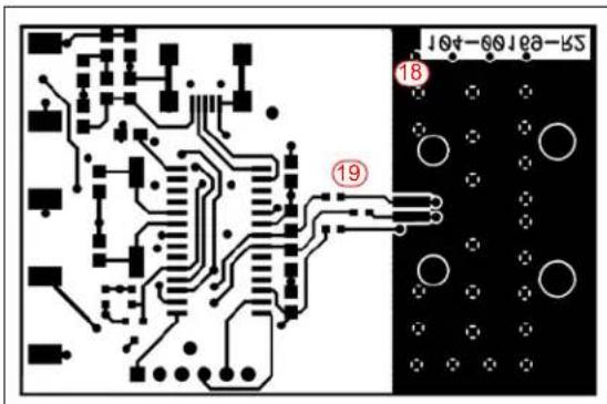
text_image
SK-03109-40T 18 19FIGURE 43: 4 ^th Layer – Bottom Metal.
- Metal fill, connected to the ground plane, minimizes thermal gradients at the cold junction.
- The digital traces that run under the ground plane extension have series resistors inserted inside the FR4 gap. This reduces the thermal conduction between the sides that solid traces would produce; otherwise this would become the worst case thermal conductor between the microcontroller and the temperature sensors.
SUMMARY
This application note covers thermal effects on Printed Circuit Boards (PCB) encountered in high (DC) precision op amp circuits. Causes, effects and fixes have been covered.
Thermocouple junctions are everywhere on a PCB. The Seebeck effect tells us that these junctions create a thermoelectric voltage. This was shown to produce a voltage across resistors (and other components) in the presence of a temperature gradient.
Preventing large thermoelectric voltages from occurring is usually the most efficient way to deal with thermocouple junctions. The amount of heat generated on the PCB can be reduced, and the heat flow redirected away from critical circuit areas. It also pays to keep any temperature changes from occurring too quickly.
Any remaining thermoelectric voltage effects need to be reduced. Choosing the metals, in critical areas, to have approximately the same work function will minimize the thermoelectric coefficients of the metal junctions. Critical components can be oriented so that they follow constant temperature contour lines. It is possible to cancel most of the thermoelectric voltage effects at the input of op amps by correctly orienting them. Smaller components, spaced closer together, will also help.
Once a design has been implemented on a PCB, it pays to measure its thermal response. Information on where to focus design effort can greatly speed up the design process. Information has been given on measuring temperature, thermal gradients, package _JA 's and troubleshooting tips and tricks.
Leakage current effects also need to be minimized. Methods to accomplish this for surface and bulk leakage currents have been shown.
Other effects were also discussed.
A design example using the MCP6V01 Thermocouple Auto-zeroed Reference Design PCB illustrates the theory and recommendations given in this application note. The circuit operation is described, then the PCB layout choices are covered in detail.
At the end of this application note, references to the literature and an appendix with the design example's schematic are provided.
REFERENCES
Related Application Notes
[1] AN990, "Analog Sensor Conditioning Circuits – An Overview," Kumen Blake; Microchip Technology Inc., DS00990, 2005.
[2] AN1177, "Op Amp Precision Design: DC Errors," Kumen Blake; Microchip Technology Inc., DS01177, 2008.
[3] AN1228, "Op Amp Precision Design: Random Noise," Kumen Blake; Microchip Technology Inc., DS01228, 2008.
Other Application Notes
[4] AN990, "Analog Sensor Conditioning Circuits – An Overview," Kumen Blake; Microchip Technology Inc., 2005.
[5] AN684, "Single Supply Temperature Sensing with Thermocouples," Bonnie C. Baker; Microchip Technology Inc., DS00684, 1998.
[6] AN679, "Temperature Sensing Technologies," Bonnie Baker, "Microchip Technology Inc., DS00679, 1998.
Other References
[7] User's Guide, "MCP6V01 Thermocouple Auto-Zeroed Reference Design," Microchip Technology Inc., DS51738, 2008.
[8] "The OMEGA ^® Made in the USA Handbook™," Vol. 1, OMEGA Engineering, Inc., 2002.
APPENDIX A: PCB SCHEMATIC (MCP6V01 THERMOCOUPLE AUTO-ZEROED REFERENCE DESIGN)
text_image
J2 HDR1X6 N/C VDD R5 10K VDD R5 XLERI U1 RG7/RV+RE3 RA0/AN0 VSSU RA1/AN1 RA2/AN2/WU-ACV+2 RA3/AN3/VIE+ RA4/TOCKI/C1OUTRCV RA5/AN4/S5/ILVDIN/C2 OSC/CLKI OSC2/CLKO/RA6 C10 20 MHz C11 22pF C8 0.47uF PIC18F2550-SOIC28 L1 1 OHM C3 10uF C2 1uF C4 10uF R3 1 3 4 5 R4 100K J3 USB Conn VDD R3 1 OHM C3 10uF C2 1uF C13 0.1uF 2nd Order RC Low-Pass Filter VOUT2 R12 499 C7 0.1uF VOUT1 R6 100 R7 100 R8 100K VREF R10 5.6K R11 100K VDD TP2 TP3 TP4 TP5 TP1 VDD TP2 TP3 TP4 TP5FIGURE A-1: THERMOCOUPLE CIRCUIT'S SCHEMATIC.
APPENDIX B: PCB PARASITIC RESISTANCE
The body of this application note emphasized better PCB designs. For this reason, detailed analyses of leakage currents were not included.
This appendix shows you how to estimate parasitic resistances on a PCB. This will help adjust designs sensitive to leakage currents.
B.1 PCB Resistivities
Surface resistivity ( _S , in units of MΩ, or equivalent) describes the local, physical behavior of a PCB surface under a voltage gradient field. The aggregate behavior over all such points creates an equivalent, parasitic surface resistance ( R_PS ) between any two points.
Bulk resistivity ( _V , in units of MΩ cm, or equivalent) describes the local, physical behavior inside a PCB's dielectric under a voltage gradient field. The aggregate behavior over all such points creates an equivalent, parasitic bulk resistance ( R_PB ) between any two points.
Typical resistivities for FR4, based on several manufacturer's data, are:
$$ \cdot \rho_ {S} \approx 1 \times 1 ^ {5} \Omega M \Omega $$
$$ \cdot \rho_ {V} \approx 1 \times 1 ^ {6} \Omega M \Omega \quad c m $$
Different operating conditions and manufacturing flows will produce different values; sometimes by two or three orders of magnitude in either direction.
B.2 Measuring Resistivities
Example B-1 shows two parallel, serpentine traces on the same PCB surface. This geometry is useful for measuring _S on a given PCB process. Make the traces as long as possible, and as close together as possible, to maximize the surface leakage current.
For example, a 6 in × 6 in PCB (60 mil thick) could have two serpentine traces 10 mil wide and 10 mil apart. If the overlap area is 5 in × 5 in, the equivalent length would be 1250 in. With _S = 1 × 10^5 M and _V ≈ 1 × 10^6 M cm, we estimate R_S ≈ 0.8 M and R_PB ≈ 2 G .
EXAMPLE B-1: PARALLEL TRACES
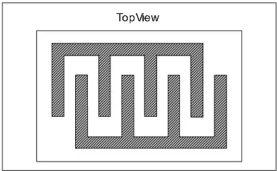
natural_image
Top view diagram of a maze-like geometric pattern with shaded and unshaded regions (no text or symbols)Example B-2 shows two parallel planes on opposite PCB surfaces. This geometry is useful for measuring _V on a given PCB process. Make the planes as large as possible, to maximize the bulk leakage current.
For instance, a 6 in × 6 in PCB (60 mil thick) could have two planes 5 in long and 5 in wide. With _S = 1 × 10^6 M and _V = 1 × 10^6 M cm, we can estimate R_PS ≈ and R_PB ≈ 0.9 G .
EXAMPLE B-2: PARALLEL PLANES

text_image
TopView End View Side ViewBe sure to measure _S and _V under various conditions seen by your circuit. These values will also change between different manufacturers and processes.
B.3 Numerical Solutions
B.3.1 COMMERCIAL SOFTWARE
When optimizing a complicated PCB geometry, it may pay to use a PDE (partial differential equation) solver. Searching the internet for “partial differential equation software,” or the equivalent, should bring up several commercially available software packages.
B.3.2 USING SPICE
It is possible to use SPICE to implement a network of resistors representing heat flow between adjacent points.
Select an array of equally spaced points. Resistors connect adjacent points and represent the local resistance to current flow, in that direction.
To simulate a particular parasitic resistance, force a voltage at its input and measure the current at its output. The voltage-to-current ratio is that resistance.
Figure B-1 shows a typical array point, in a two dimensional (2D) array. The central point is at voltage V_0 . The four adjacent points are connected by the four resistors R_1 , R_2 , R_3 and R_4 .
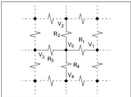
text_image
V2 R2 V0 R1 V1 V3 R3 R4 V4FIGURE B-1: TYPICAL 2D ARRAY.
The resistors represent the local resistivity between adjacent points. Use very low valued resistors for points connected by metal. For instance, R_1 is:
EQUATION B-1:
$$ \begin{array}{l} R _ {1} = \rho_ {S} \Delta x / \Delta y, \text { for surface calculations } \ = \rho_ {V} \Delta x / (\Delta y \Delta z), \quad \text { for bulk calculations } \ \rho_ {S} = \text { Local Surface Resistivity } (M \Omega) \ \rho_ {V} = \text { Local Bulk Resistivity } (M \Omega \quad c m) \ \Delta x = \text { grid spacing in the } x \text {-direction} \ \Delta y = \text { grid spacing in the y - direction } \ \Delta z = z \text {-dimension (common to all objects)} \ \end{array} $$
Where:
This approach is easily extended to three dimensions (3D).
B.3.3 USING A SPREADSHEET
It is possible to simulate in a spreadsheet by using an iterative approach. Set up the resistive array like the last section. The iteration equation at V_0 is:
EQUATION B-2:
$$ V _ {0} = \left(V _ {1} / R _ {1} + V _ {2} / R _ {2} + V _ {3} / R _ {3} + V _ {4} / R _ {4}\right) $$
$$ / \left(1 / R + 1 / R _ {2} + 1 / R _ {3} + 1 / R _ {4}\right) $$
$$ = (V _ {1} + V _ {2} + V _ {3} + V _ {4}) / 4, \text { all Rs equal } $$
The convergence can be slow, so this approach should be used for simple problems.
Once the voltages are determined, it is a simple matter to calculate the sum of currents into (or out of) a node of interest.
This approach is easily extended to three dimensions (3D).
APPENDIX C: REVISION HISTORY
Revision B (July 2012)
The following is the list of modifications:
- Added power supply components to circuit diagrams.
- Re-wrote Section "Leakage Currents", starting on page 11.
a) Added information on high impedance sources and parasitic leakage resistances.
b) Corrected guard ring connections so they are driven by a low impedance source.
c) Added current source examples.
d) Added discussion of bulk leakage currents.
e) Expanded discussion on isolating sensitive connections from a PCB.
- Added Section "Other Tips", on page 16.
- Added AN990 to Section "References", on page 19.
- Added Appendix B: "PCB Parasitic Resistance", starting on page 21.
- Added Appendix C: "Revision History", on page 23.
Revision A (March 2009)
• Original Release of this Document.
NOTES:
Note the following details of the code protection feature on Microchip devices:
• Microchip products meet the specification contained in their particular Microchip Data Sheet.
- Microchip believes that its family of products is one of the most secure families of its kind on the market today, when used in the intended manner and under normal conditions.
- There are dishonest and possibly illegal methods used to breach the code protection feature. All of these methods, to our knowledge, require using the Microchip products in a manner outside the operating specifications contained in Microchip's Data Sheets. Most likely, the person doing so is engaged in theft of intellectual property.
- Microchip is willing to work with the customer who is concerned about the integrity of their code.
- Neither Microchip nor any other semiconductor manufacturer can guarantee the security of their code. Code protection does not mean that we are guaranteeing the product as "unbreakable."
Code protection is constantly evolving. We at Microchip are committed to continuously improving the code protection features of our products. Attempts to break Microchip's code protection feature may be a violation of the Digital Millennium Copyright Act. If such acts allow unauthorized access to your software or other copyrighted work, you may have a right to sue for relief under that Act.
Information contained in this publication regarding device applications and the like is provided only for your convenience and may be superseded by updates. It is your responsibility to ensure that your application meets with your specifications. MICROCHIP MAKES NO REPRESENTATIONS OR WARRANTIES OF ANY KIND WHETHER EXPRESS OR IMPLIED, WRITTEN OR ORAL, STATUTORY OR OTHERWISE, RELATED TO THE INFORMATION, INCLUDING BUT NOT LIMITED TO ITS CONDITION, QUALITY, PERFORMANCE, MERCHANTABILITY OR FITNESS FOR PURPOSE. Microchip disclaims all liability arising from this information and its use. Use of Microchip devices in life support and/or safety applications is entirely at the buyer's risk, and the buyer agrees to defend, indemnify and hold harmless Microchip from any and all damages, claims, suits, or expenses resulting from such use. No licenses are conveyed, implicitly or otherwise, under any Microchip intellectual property rights.
Trademarks
The Microchip name and logo, the Microchip logo, dsPIC, KEELOQ, KEELOQ logo, MPLAB, PIC, PICmicro, PICSTART, PIC ^32 logo, rfPIC and UNI/O are registered trademarks of Microchip Technology Incorporated in the U.S.A. and other countries.
FilterLab, Hampshire, HI-TECH C, Linear Active Thermistor, MXDEV, MXLAB, SEEVAL and The Embedded Control Solutions Company are registered trademarks of Microchip Technology Incorporated in the U.S.A.
Analog-for-the-Digital Age, Application Maestro, chipKIT, chipKIT logo, CodeGuard, dsPICDEM, dsPICDEM.net, dsPICworks, dsSPEAK, ECAN, ECONOMONITOR, FanSense, HI-TIDE, In-Circuit Serial Programming, ICSP, Mindi, MiWi, MPASM, MPLAB Certified logo, MPLIB, MPLINK, mTouch, Omniscient Code Generation, PICC, PICC-18, PICDEM, PICDEM.net, PICkit, PICtail, REAL ICE, rfLAB, Select Mode, Total Endurance, TSHARC, UniWinDriver, WiperLock and ZENA are trademarks of Microchip Technology Incorporated in the U.S.A. and other countries.
SQTP is a service mark of Microchip Technology Incorporated in the U.S.A.
All other trademarks mentioned herein are property of their respective companies.
© 2009-2012, Microchip Technology Incorporated, Printed in the U.S.A., All Rights Reserved.

Printed on recycled paper.
QUALITY MANAGEMENT SYSTEM
CERTIFIED BY DNV
= ISO/TS 16949=
ISBN: 978-1-62076-404-6
Microchip received ISO/TS-16949:2009 certification for its worldwide headquarters, design and wafer fabrication facilities in Chandler and Tempe, Arizona; Gresham, Oregon and design centers in California and India. The Company's quality system processes and procedures are for its PIC® MCUs and dsPIC® DSCs, KEELoo® code hopping devices, Serial EEPROMs, microperipherals, nonvolatile memory and analog products. In addition, Microchip's quality system for the design and manufacture of development systems is ISO 9001:2000 certified.
Worldwide Sales and Service
AMERICAS
Corporate Office
2355 West Chandler Blvd.
Chandler, AZ 85224-6199
Tel: 480-792-7200
Fax: 480-792-7277
Technical Support
http://www.microchip.com/support
Web Address:
www.microchip.com
Atlanta
Duluth, GA
Tel: 678-957-9614
Fax: 678-957-1455
Boston
Westborough, MA
Tel: 774-760-0087
Fax: 774-760-0088
Chicago
Itasca,
Tel: 630-285-0071
Fax: 630-285-0075
Cleveland
Independence, OH
Tel: 216-447-0464
Fax: 216-447-0643
Dallas
Addison, TX
Tel: 972-818-7423
Fax: 972-818-2924
Detroit
Farmington Hills, MI
Tel: 248-538-2250
Fax: 248-538-2260
Indianapolis
Noblesville, IN
Tel: 317-773-8323
Fax: 317-773-5453
Los Angeles
Mission Viejo, CA
Tel: 949-462-9523
Fax: 949-462-9608
Santa Clara
Santa Clara, CA
Tel: 408-961-6444
Fax: 408-961-6445
Toronto
Mississauga, Ontario,
Canada
Tel: 905-673-0699
Fax: 905-673-6509
ASIA/PACIFIC
Asia Pacific Office
Suites 3707-14, 37th Floor
Tower 6, The Gateway
Harbour City, Kowloon
Hong Kong
Tel: 852-2401-1200
Fax: 852-2401-3431
Australia - Sydney
Tel: 61-2-9868-6733
Fax: 61-2-9868-6755
China - Beijing
Tel: 86-10-8569-7000
Fax: 86-10-8528-2104
China - Chengdu
Tel: 86-28-8665-5511
Fax: 86-28-8665-7889
China - Chongqing
Tel: 86-23-8980-9588
Fax: 86-23-8980-9500
China - Hangzhou
Tel: 86-571-2819-3187
Fax: 86-571-2819-3189
China - Hong Kong SAR
Tel: 852-2401-1200
Fax: 852-2401-3431
China - Nanjing
Tel: 86-25-8473-2460
Fax: 86-25-8473-2470
China - Qingdao
Tel: 86-532-8502-7355
Fax: 86-532-8502-7205
China - Shanghai
Tel: 86-21-5407-5533
Fax: 86-21-5407-5066
China - Shenyang
Tel: 86-24-2334-2829
Fax: 86-24-2334-2393
China - Shenzhen
Tel: 86-755-8203-2660
Fax: 86-755-8203-1760
China - Wuhan
Tel: 86-27-5980-5300
Fax: 86-27-5980-5118
China - Xian
Tel: 86-29-8833-7252
Fax: 86-29-8833-7256
China - Xiamen
Tel: 86-592-2388138
Fax: 86-592-2388130
China - Zhuhai
Tel: 86-756-3210040
Fax: 86-756-3210049
ASIA/PACIFIC
India - Bangalore
Tel: 91-80-3090-4444
Fax: 91-80-3090-4123
India - New Delhi
Tel: 91-11-4160-8631
Fax: 91-11-4160-8632
India - Pune
Tel: 91-20-2566-1512
Fax: 91-20-2566-1513
Japan - Osaka
Tel: 81-66-152-7160
Fax: 81-66-152-9310
Japan - Yokohama
Tel: 81-45-471-6166
Fax: 81-45-471-6122
Korea - Daegu
Tel: 82-53-744-4301
Fax: 82-53-744-4302
Korea - Seoul
Tel: 82-2-554-7200
Fax: 82-2-558-5932 or
82-2-558-5934
Malaysia - Kuala Lumpur
Tel: 60-3-6201-9857
Fax: 60-3-6201-9859
Malaysia - Penang
Tel: 60-4-227-8870
Fax: 60-4-227-4068
Philippines - Manila
Tel: 63-2-634-9065
Fax: 63-2-634-9069
Singapore
Tel: 65-6334-8870
Fax: 65-6334-8850
Taiwan - Hsin Chu
Tel: 886-3-5778-366
Fax: 886-3-5770-955
Taiwan - Kaohsiung
Tel: 886-7-536-4818
Fax: 886-7-330-9305
Taiwan - Taipei
Tel: 886-2-2500-6610
Fax: 886-2-2508-0102
Thailand - Bangkok
Tel: 66-2-694-1351
Fax: 66-2-694-1350
EUROPE
Austria - Wels
Tel: 43-7242-2244-39
Fax: 43-7242-2244-393
Denmark - Copenhagen
Tel: 45-4450-2828
Fax: 45-4485-2829
France - Paris
Tel: 33-1-69-53-63-20
Fax: 33-1-69-30-90-79
Germany - Munich
Tel: 49-89-627-144-0
Fax: 49-89-627-144-44
Italy - Milan
Tel: 39-0331-742611
Fax: 39-0331-466781
Netherlands - Drunen
Tel: 31-416-690399
Fax: 31-416-690340
Spain - Madrid
Tel: 34-91-708-08-90
Fax: 34-91-708-08-91
UK - Wokingham
Tel: 44-118-921-5869
Fax: 44-118-921-5820
11/29/11