EVB-LAN9354 - Carte d'extension réseau Microchip - Free user manual and instructions
Find the device manual for free EVB-LAN9354 Microchip in PDF.

User questions about EVB-LAN9354 Microchip
0 question about this device. Answer the ones you know or ask your own.
Ask a new question about this device
Download the instructions for your Carte d'extension réseau in PDF format for free! Find your manual EVB-LAN9354 - Microchip and take your electronic device back in hand. On this page are published all the documents necessary for the use of your device. EVB-LAN9354 by Microchip.
USER MANUAL EVB-LAN9354 Microchip
Note the following details of the code protection feature on Microchip devices:
• Microchip products meet the specification contained in their particular Microchip Data Sheet.
- Microchip believes that its family of products is one of the most secure families of its kind on the market today, when used in the intended manner and under normal conditions.
- There are dishonest and possibly illegal methods used to breach the code protection feature. All of these methods, to our knowledge, require using the Microchip products in a manner outside the operating specifications contained in Microchip's Data Sheets. Most likely, the person doing so is engaged in theft of intellectual property.
• Microchip is willing to work with the customer who is concerned about the integrity of their code.
- Neither Microchip nor any other semiconductor manufacturer can guarantee the security of their code. Code protection does not mean that we are guaranteeing the product as "unbreakable."
Code protection is constantly evolving. We at Microchip are committed to continuously improving the code protection features of our products. Attempts to break Microchip's code protection feature may be a violation of the Digital Millennium Copyright Act. If such acts allow unauthorized access to your software or other copyrighted work, you may have a right to sue for relief under that Act.
Information contained in this publication regarding device applications and the like is provided only for your convenience and may be superseded by updates. It is your responsibility to ensure that your application meets with your specifications. MICROCHIP MAKES NO REPRESENTATIONS OR WARRANTIES OF ANY KIND WHETHER EXPRESS OR IMPLIED, WRITTEN OR ORAL, STATUTORY OR OTHERWISE, RELATED TO THE INFORMATION, INCLUDING BUT NOT LIMITED TO ITS CONDITION, QUALITY, PERFORMANCE, MERCHANTABILITY OR FITNESS FOR PURPOSE. Microchip disclaims all liability arising from this information and its use. Use of Microchip devices in life support and/or safety applications is entirely at the buyer's risk, and the buyer agrees to defend, indemnify and hold harmless Microchip from any and all damages, claims, suits, or expenses resulting from such use. No licenses are conveyed, implicitly or otherwise, under any Microchip intellectual property rights unless otherwise stated.
Trademarks
The Microchip name and logo, the Microchip logo, dsPIC, FlashFlex, flexPWR, JukeBlox, KEELOQ, KEELOQ logo, Kleer, LANCheck, MediaLB, MOST, MOST logo, MPLAB, OptoLyzer, PIC, PICSTART, PIC ^32 logo, RightTouch, SpyNIC, SST, SST Logo, SuperFlash and UNI/O are registered trademarks of Microchip Technology Incorporated in the U.S.A. and other countries.
The Embedded Control Solutions Company and mTouch are registered trademarks of Microchip Technology Incorporated in the U.S.A.
Analog-for-the-Digital Age, BodyCom, chipKIT, chipKIT logo, CodeGuard, dsPICDEM, dsPICDEM.net, ECAN, In-Circuit Serial Programming, ICSP, Inter-Chip Connectivity, KleerNet, KleerNet logo, MiWi, MPASM, MPF, MPLAB Certified logo, MPLIB, MPLINK, MultiTRAK, NetDetach, Omniscient Code Generation, PICDEM, PICDEM.net, PICkit, PICtail, RightTouch logo, REAL ICE, SQI, Serial Quad I/O, Total Endurance, TSHARC, USBCheck, VariSense, ViewSpan, WiperLock, Wireless DNA, and ZENA are trademarks of Microchip Technology Incorporated in the U.S.A. and other countries.
SQTP is a service mark of Microchip Technology Incorporated in the U.S.A.
Silicon Storage Technology is a registered trademark of Microchip Technology Inc. in other countries.
GestIC is a registered trademark of Microchip Technology Germany II GmbH & Co. KG, a subsidiary of Microchip Technology Inc., in other countries.
All other trademarks mentioned herein are property of their respective companies.
© 2015, Microchip Technology Incorporated, Printed in the U.S.A., All Rights Reserved.
ISBN: 978-1-63277-588-7
QUALITY MANAGEMENT SYSTEM
CERTIFIED BY DNV
=ISO/TS 16949=
Microchip received ISO/TS-16949:2009 certification for its worldwide headquarters, design and wafer fabrication facilities in Chandler and Tempe, Arizona; Gresham, Oregon and design centers in California and India. The Company's quality system processes and procedures are for its PIC® MCUs and dsPIC® DSCs, KEELoo® code hopping devices, Serial EEPROMs, microperipherals, nonvolatile memory and analog products. In addition, Microchip's quality system for the design and manufacture of development systems is ISO 9001:2000 certified.
Object of Declaration: EVB-LAN9354
EU Declaration of Conformity
This declaration of conformity is issued by the manufacturer.
The development/evaluation tool is designed to be used for research and development in a laboratory environment. This development/evaluation tool is not a Finished Appliance, nor is it intended for incorporation into Finished Appliances that are made commercially available as single functional units to end users under EU EMC Directive 2004/108/EC and as supported by the European Commission's Guide for the EMC Directive 2004/108/EC (8 ^th February 2010).
This development/evaluation tool complies with EU RoHS2 Directive 2011/65/EU.
For information regarding the exclusive, limited warranties applicable to Microchip products, please see Microchip's standard terms and conditions of sale, which are printed on our sales documentation and available at www.microchip.com.
Signed for and on behalf of Microchip Technology Inc. at Chandler, Arizona, USA
Derek Carlson
Derek Carlson
VP Development Tools
16-July-2013 Date
NOTES:
Table of Contents
Preface 7
Introduction....7
Document Layout 7
Conventions Used in this Guide 8
The Microchip Web Site 9
Development Systems Customer Change Notification Service 9
Customer Support 9
Document Revision History 10
Chapter 1. Overview
1.1 Introduction ...... 11
1.1.1 References 12
1.1.2 Terms and Abbreviations ...... 12
Chapter 2. Board Details
2.1 Board Details 14
2.1.1 Power 14
2.1.2 Power-on Reset 15
2.1.3 Clock 15
Chapter 3. Board Configuration
3.1 Strap Options 16
3.1.3 Link Partner Duplex/Speed Configurations 19
3.1.4 P0 Configurations 20
3.1.5 RMII RX Clock Configurations 20
3.1.6 GPIO Header 21
3.1.7 I2C Aardvark Header 21
3.1.8 Copper and Fiber Mode Selections 21
3.1.8.1 Copper Mode 23
3.1.8.2 Fiber Mode 22
3.1.8.3 FX-LOS Fiber Mode Strap 23
3.2 LEDs 23
3.3 Test Points 23
3.4 Mechanicals 24
Appendix A. EVB-LAN9354 Evaluation Board
A.1 Introduction 25
Appendix B. EVB-LAN9354 Evaluation Board Schematics
B.1 Introduction 26
Appendix C. Bill of Materials (BOM)
C.1 Introduction 34
Wordwide Sales and Service ....38
Preface
NOTICE TO CUSTOMERS
All documentation becomes dated, and this manual is no exception. Microchip tools and documentation are constantly evolving to meet customer needs, so some actual dialogs and/or tool descriptions may differ from those in this document. Please refer to our web site (www.microchip.com) to obtain the latest documentation available.
Documents are identified with a "DS" number. This number is located on the bottom of each page, in front of the page number. The numbering convention for the DS number is "DSXXXXXA", where "XXXXX" is the document number and "A" is the revision level of the document.
For the most up-to-date information on development tools, see the MPLAB ^® IDE online help. Select the Help menu, and then Topics to open a list of available online help files.
INTRODUCTION
This chapter contains general information that will be useful to know before using the EVB-LAN9354. Items discussed in this chapter include:
- Document Layout
- Conventions Used in this Guide
• The Microchip Web Site - Development Systems Customer Change Notification Service
- Customer Support
• Document Revision History
DOCUMENT LAYOUT
This document describes how to use the EVB-LAN9354 Evaluation Board as a development tool for the LAN9354 three-port 10/100 managed Ethernet switch. The manual layout is as follows:
- Chapter 1. “Overview” – Shows a brief description of the EVB-LAN9354 Evaluation Board.
- Chapter 2. “Getting Started” – Includes instructions on how to get started with the EVB-LAN9354 Evaluation Board.
- Chapter 3. “Board Configuration” – Provides information about the EVB-LAN9354 Evaluation Board battery charging features.
- Appendix A. "EVB-LAN9354 Evaluation Board" – This appendix shows the EVB-LAN9354 Evaluation Board.
- Appendix B. "EVB-LAN9354 Evaluation Board Schematics" – This appendix shows the EVB-LAN9354 Evaluation Board schematics.
- Appendix C. "Bill of Materials (BOM)" – This appendix includes the EVB-LAN9354 Evaluation Board Bill of Materials (BOM).
CONVENTIONS USED IN THIS GUIDE
This manual uses the following documentation conventions:
DOCUMENTATION CONVENTIONS
| Description Represents Examples | ||
| Arial font: | ||
| Italic characters Referenced books | oks MPLAB | ^ IDE User's Guide |
| Emphasized text ...is the only compiler... | ||
| Initial caps A window the Output | window | |
| A dialog the Settings dialog | ||
| A menu selection select Enable Programmer | ||
| Quotes A field name in a window or dialog | "Save project before build" | |
| Underlined, italic text with right angle bracket | A menu path File>Save | —— |
| Bold characters A dialog button | Click OK | |
| A tab | Click the Power tab | |
| N'Rnnnn | A number in verilog format, where N is the total number of digits, R is the radix and n is a digit. | 4'b0010, 2'hF1 |
| Text in angle brackets <> | A key on the keyboard | Press,, |
| Courier New font: | ||
| Plain Courier New | Sample source code | #define START |
| Filenames | autoexec.bat | |
| File paths | c:\mccl8\h | |
| Keywords | _asm, _endasm, static | |
| Command-line options | -Opa+, -Opa- | |
| Bit values | 0, 1 | |
| Constants | 0xFF, 'A' | |
| Italic Courier New | A variable argument | file.o, where file can be any valid filename |
| Square brackets [] | Optional arguments | mccl8 [options] file [options] |
| Curly brackets and pipe character: { | } | Choice of mutually exclusive arguments; an OR selection | errorlevel {0|1} |
| Ellipses... Replaces repeated text var_name [, | var_name...] | |
| Represents code supplied by user void main (void) { ... } | ||
Microchip provides online support via our web site at www.microchip.com. This web site is used as a means to make files and information easily available to customers. Accessible by using your favorite Internet browser, the web site contains the following information:
- Product Support – Data sheets and errata, application notes and sample programs, design resources, user's guides and hardware support documents, latest software releases and archived software
- General Technical Support – Frequently Asked Questions (FAQs), technical support requests, online discussion groups, Microchip consultant program member listing
- Business of Microchip – Product selector and ordering guides, latest Microchip press releases, listing of seminars and events, listings of Microchip sales offices, distributors and factory representatives
DEVELOPMENT SYSTEMS CUSTOMER CHANGE NOTIFICATION SERVICE
Microchip's customer notification service helps keep customers current on Microchip products. Subscribers will receive e-mail notification whenever there are changes, updates, revisions or errata related to a specified product family or development tool of interest.
To register, access the Microchip web site at www.microchip.com, click on Customer Change Notification and follow the registration instructions.
The Development Systems product group categories are:
- Compilers – The latest information on Microchip C compilers, assemblers, linkers and other language tools. These include all MPLAB C compilers; all MPLAB assemblers (including MPASM assembler); all MPLAB linkers (including MPLINK object linker); and all MPLAB librarians (including MPLIB object librarian).
- Emulators – The latest information on Microchip in-circuit emulators. This includes the MPLAB REAL ICE and MPLAB ICE 2000 in-circuit emulators.
- In-Circuit Debuggers – The latest information on the Microchip in-circuit debuggers. This includes MPLAB ICD 3 in-circuit debuggers and PICkit 3 debug express.
- MPLAB IDE – The latest information on Microchip MPLAB IDE, the Windows Integrated Development Environment for development systems tools. This list is focused on the MPLAB IDE, MPLAB IDE Project Manager, MPLAB Editor and MPLAB SIM simulator, as well as general editing and debugging features.
- Programmers – The latest information on Microchip programmers. These include production programmers such as MPLAB REAL ICE in-circuit emulator, MPLAB ICD 3 in-circuit debugger and MPLAB PM3 device programmers. Also included are nonproduction development programmers such as PICSTART Plus and PIC-kit 2 and 3.
CUSTOMER SUPPORT
Users of Microchip products can receive assistance through several channels:
• Distributor or Representative
- Local Sales Office
• Field Application Engineer (FAE)
- Technical Support
Customers should contact their distributor, representative or field application engineer (FAE) for support. Local sales offices are also available to help customers. A listing of sales offices and locations is included in the back of this document.
Technical support is available through the web site at:
http://www.microchip.com/support
DOCUMENT REVISION HISTORY
Revision A (July 2015)
- Initial Release of this Document.
Chapter 1. Overview
1.1 INTRODUCTION
The LAN9354 is a fully featured, three-port 10/100 managed Ethernet switch designed for industrial and embedded applications where performance, flexibility, ease of integration and system cost control are required.
The LAN9354 combines all the functions of a 10/100 switch system, including the switch fabric, packet buffers, buffer manager, media access controllers (MACs), PHY transceivers, and serial management. IEEE 1588v2 is supported via the integrated IEEE 1588v2 hard-ware time stamp unit, which supports end-to-end and peer-to-peer transparent clocks.
The LAN9354 complies with the IEEE 802.3 (full/half-duplex 10BASE-T and 100BASE-TX) Ethernet protocol, IEEE 802.3az Energy Efficient Ethernet (EEE) (100Mbps only), and 802.1D/802.1Q management protocol specifications, enabling compatibility with industry standard Ethernet and Fast Ethernet applications.
100BASE-FX is supported via an external fiber transceiver and cable diagnostics (short, open and length) is included on the internal twisted pair copper interface.
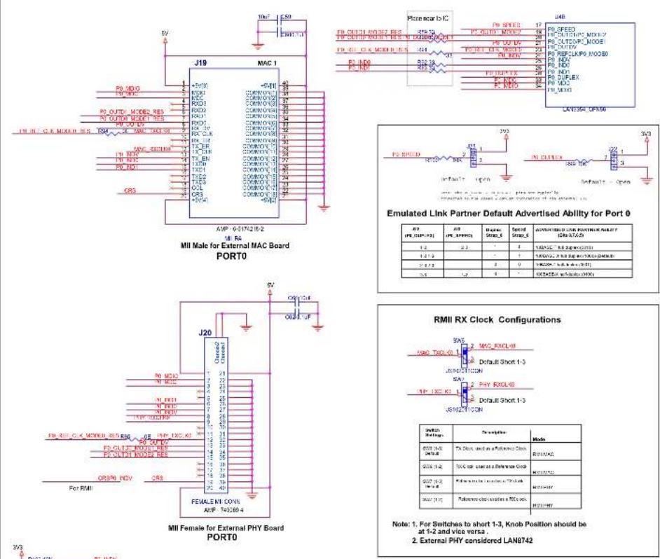
The EVB-LAN9354 is an Evaluation Board (EVB) that utilizes the LAN9354 to provide a fully-functional three-port Ethernet switch with Single RMII. The EVB-LAN9354 provides two fully integrated MAC/PHY internet ports (Ports 1 & 2) via on-board RJ45 connectors. Port 0 provides two MII port connectors which support the following:
- An external RMII-Capable MAC (with LAN9354 in PHY mode), via the on-board 40-pin male MII connector
- An external RMII-Capable PHY (with LAN9354 in MAC mode), via the on-board 40-pin female MII connector
Power is supplied to the board via a +5V external wall mount power supply.
The EVB-LAN9354 includes a 64K x 8 I2C EEPROM that may be used to automatically load configuration settings from the EEPROM into the device at reset. An I2C host adapter interface header (10-pin, 2x5) is provided to simplify I2C based configuration. A simplified block diagram of the EVB-LAN9354 can be seen in Figure 1-1.
FIGURE 1-1: EVB-LAN9354 BLOCK DIAGRAM

flowchart
graph TD
    A["40 pin MII Connector (Female)"] --> B["Port 0"]
    C["40 pin MII Connector (Male)"] --> B
    B --> D["Microchip LAN9354"]
    D --> E["Port 1"]
    D --> F["Port 2"]
    E --> G["Fiber Transceiver (SFP)"]
    F --> H["Fiber Transceiver (SFP)"]
    G --> I["10/100 Ethernet Magnetics & RJ45"]
    H --> J["10/100 Ethernet Magnetics & RJ45"]
    I --> K["Straps Jumpers"]
    J --> L["Reset"]
    K --> M["Mode Switch"]
    L --> N["Power Supply Module"]
    M --> O["RMII"]
    N --> P["5V"]
    O --> Q["To External PHY"]
    P --> R["To External MAC"]
    Q --> S["Ethernet"]
    R --> T["Ethernet"]
1.1.1 References
Concepts and material available in the following documents may be helpful when reading this document. Visit www.microchip.com for the latest documentation.
| Document Location | |
| LAN9354 datasheet Visit | www.microchip.com |
| AN8-13 Suggested Magnetics | http://www.microchip.com/wwwAp-pNotes/AppNotes.aspx?appnote=en562793 |
| EVB-LAN9354 Evaluation Board Schematic | Visit www.microchip.com |
1.1.2 Terms and Abbreviations
• EVB - Evaluation Board
• DNP - Do Not Populate
• 100BASE-TX - 100 Mbps Fast Ethernet, IEEE802.3u Compliant
• GPIO - General Purpose I/O
• MII - Media Independent Interface
• RMII - Reduced Media Independent Interface
- EEE - Energy-Efficient Ethernet
• SFP - Small Form-factor Pluggable
• SFF - Small Form Factor
• SMI - Serial Management Interface
Chapter 2. Board Details
2.1 BOARD DETAILS
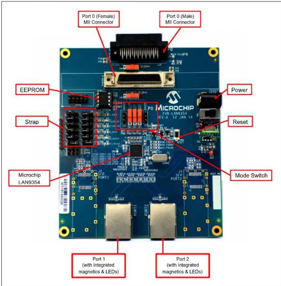
The following sections describe the various board features, including jumpers, LEDs, test points, system connections, and switches. A top view of the EVB-LAN9354 is shown in Figure 2-1.
FIGURE 2-1: LAN9354 BOARD REV-A
text_image
Port 0 (Female) MII Connector Port 0 (Male) MII Connector EEPROM Strap Microchip LAN9354 Power Reset Mode Switch Port 1 (with integrated magnetics & LEDs) Port 2 (with integrated magnetics & LEDs)2.1.1 Power
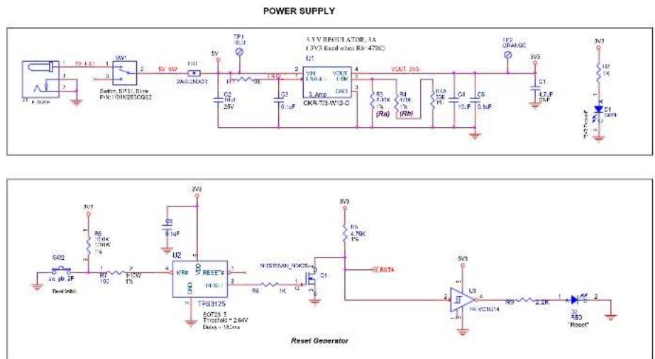
DC 5V is applied through (J1) DC Socket, powered by a +5V external wall adapter switch (SW1) need to be ON position for the 5V to reach the 3.3V regulator. Glowing of Green LED (D1) indicates successful generation of 3.3V o/p. This Power is supplied to the LAN9354 and it has internal 1.2 V regulator which supplies power to the internal core logic.
2.1.2 Power-on Reset
A power-on reset occurs whenever power is initially applied to the LAN9354 or if the power is removed and reapplied to the LAN9354. This event resets all circuitry within the LAN9354. After initial power-on, the LAN9354 can be reset by pressing the reset switch (SW2). The reset LED D2 will assert (red) when the LAN9354 is in reset condition.
For stability, a delay of approximately 180ms is added from the +3.3V o/p to reset release.
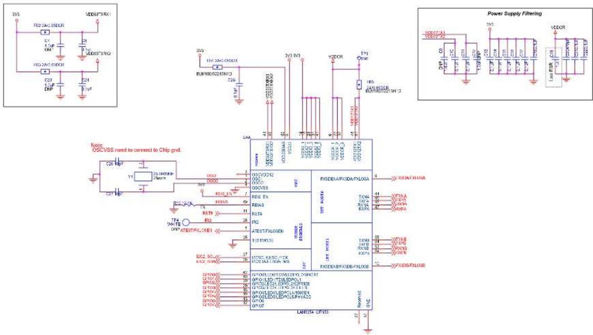
2.1.3 Clock
The LAN9354 requires a fixed-frequency 25 MHz clock ( ± 50 ppm) source for use by the internal clock oscillator and PLL. This is typically provided by attaching a 25 MHz crystal to the OSCI and OSCO pins. Optionally, this clock can be provided by driving the OSCI input pin with a single-ended 25 MHz clock source.
Chapter 3. Board Configuration
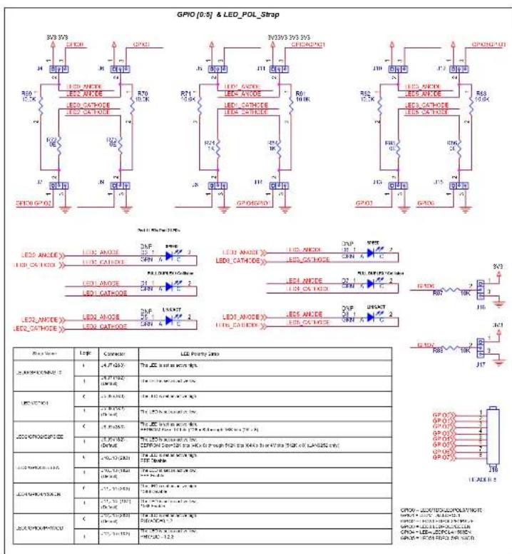
3.1 STRAP OPTIONS
The following tables describe the default settings and jumper descriptions for the EVB-LAN9354. These defaults are the recommended configurations for evaluation of the LAN9354. These settings may be changed as needed, however, any deviation from the defaults settings should be approached with care and knowledge of the schematics and datasheet. An incorrect jumper setting may disable the board.
Jumpers J4 through J15 set various functions of the LAN9354. They can also be used as GPIOs, LED drivers. When used as LED drivers, as they are on the EVB-LAN9354, they are connected a specific way to set the strap value to a "1", and another way to set the strap value to a "0". Figure 3-1 illustrates the schematics connections with the D3 circuit as a pull-up, and the D4 circuit as a pull-down. To illuminate D3, the LAN9354 will drive the cathode of the D3 low. To illuminate D4, the LAN9354 will drive the cathode of the D4 high.
The J4 - J15 jumpers must be configured in pairs to identical settings in order to realize the D3 circuit or the D4 circuit. The pairings are as follows:
- J 4 & J 7
- J 6 & J 9
- J 5 & J 8
- J11 & J14
- J10 & J13
- J12 & J15
The following subsections detail the jumper pair settings, their associated strap settings, and the functional effects of setting the straps. All strap values are read during power-up and on the rising edge of nRST signal. Once the strap value is set, the LAN9354 will drive the LED's high or low for illumination according the strap value. For other designs which may use these pins as GPIOs refer to LAN9354 datasheet for additional information. In those cases, internal default straps must be changed by an I2C or SMI master or through EEPROM fields.
FIGURE 3-1: LED STRAP CIRCUIT

text_image
+3.3V R72 1K R69 10K D3 Strap Pullup Strap Pulldown D4 R71 10K R74 1K3.1.1.1 GPIO/LED POL/LED CONFIGURATIONS:
GPIO/LED POL/LED configuration straps are used to configure the default polarity of LEDs, GPIOs through jumpers as shown below in Table 3-1.
TABLE 3-1: GPIO/LED POL/LED CONFIGURATIONS
| Header Pin | Settings Signal Name | Strap Value Description | |
| J4 & J7 1-2(default) | LEDPOL0 | /GPIO0/LED0LED (D3) is | 1 The LED (D3) isset as activeLOW. |
| 2 -3 0 The | |||
| J5 & J8 1-2(default) | LEDPOL1 | /GPIO1/LED1LED (D4) is | 1 The LED (D4) isset as activeLOW. |
| 2 -3 0 The | |||
| J6 & J9 1-2(default) | LEDPOL2 | /GPIO2/LED2LED (D5) is | 1 The LED (D5) isset as activeLOW. |
| 2 -3 0 The | |||
| J10 & J13 | 1-2(default) | DPOL3/GPIO3/LED3LED (D6) is | 1 The LED (D6) isset as activeLOW. |
| 2 -3 0 The |
TABLE 3-1: GPIO/LED POL/LED CONFIGURATIONS (CONTINUED)
| Header | Pin Settings | Signal Name | Strap Value | Description |
| J11 & J14 1-2 (default) LEDPOL4 | /GPIO4/LED4LED (D7) is | 1 The LED (D7) is set as active LOW. | ||
| 2 -3 0 The | set as active HIGH. | |||
| J12 & J15 1-2 (default) LEDPOL5 | /GPIO5/LED5LED (D8) is | 1 The LED (D8) is set as active LOW. | ||
| 2 -3 0 The | set as active HIGH. | |||
3.1.1.2 SERIAL MANAGEMENT MODE CONFIGURATION
Serial Management Mode selection strap is used to configure the default value of the Serial Management Mode Strap hard-strap (serial_mngt_mode_strap) through jumpers as shown below in Table 3-2.
TABLE 3-2: SERIAL MANAGEMENT MODE CONFIGURATION
| Header Pin Settings | serial_mngt_mode_strap | Description | |
| J4 & J7 2-3 0 | SMI Managed | Mode | |
| J4 & J7 | 1-2 (default) | 1 | I2C Managed Mode |
3.1.1.3 EEPROM SIZE CONFIGURATION:
The EEPROM size configuration strap (J6 & J9) determines the supported EEPROM size range. A low selects 1Kbits (128 x 8) through 16Kbits (2K x 8)_24C16. A high selects 32Kbits (4K x 8) through 512Kbits (64K x 8) or 4Mbits (512K x 8)_24C512 as shown below in Table 3-3.
TABLE 3-3: EEPROM SIZE CONFIGURATION
| Header Pin Settings | eeprom_size_strap Value | Description | |
| J6 & J9 | 1-2 (default) | 1 | EEPROM size = 32K bits (4k x 8) through 512K bits (64K x 8) |
| 2 -3 | 0 | EEPROM size = 1K bits (128 x 8) through 16K bits (2K x 8) | |
3.1.1.4 ENERGY-EFFICIENT ETHERNET CONFIGURATION
EEE_EN configuration strap is used to configure the default value of the EEE Enable 2-1 soft-straps (EEE_enable_strap_[2:1]) through jumpers as shown below in Table3-4.
TABLE 3-4: EEE_EN CONFIGURATION
| Header Pin Settings | EEE_enable_strap_[2:1] Value | Description | |
| J10 & J13 | 1-2(default) | 1 | EEE Enable |
| 2 -3 | 0 | EEE Disable | |
3.1.1.5 1588 ENABLE CONFIGURATION
Energy Efficient Ethernet configuration strap is used to configure the default value of the 1588 Enable soft-strap (1588_enable_strap) through jumpers as shown below in Table 3-5.
TABLE 3-5: 1588 ENABLE CONFIGURATION
| Header Pin Settings | 1588_enable_strap Value | Description |
| J11 & J14 1-2 (default) 1 1588 Enable | ||
| 2 -3 0 1588 Disable | ||
3.1.1.6 PHY ADDRESS CONFIGURATION
PHY Address selection strap is used to configure the default value of the Switch PHY Address Select soft-strap (phy_addr_sel_strap) through jumpers as shown below in Table 3-6.
TABLE 3-6: PHY ADDRESSING
| Header | Pin Settings | PHY_ADDR_SEL _STRAP Value | VIRTUAL PHY 0 AND 1 DEFAULT ADDRESS VALUE | PHY A DEFAULT ADDRESS VALUE | PHY B DEFAULT ADDRESS VALUE |
| J12 & J15 | 1-2 | 1 | 1 | 2 | 3 |
| 2-3 (default) | 0 | 0 | 1 | 2 |
3.1.2 GPIO 6 & GPIO 7 Input and Output Configurations
GPIO 6 & 7 configuration straps are used to configure the default input value of the GPIO 6 and 7 through jumpers as shown below in Table 3-7 and Table 3-8.
TABLE 3-7: GPIO 6 & 7 INPUT CONFIGURATION
| Header Pin Settings | Input | Signal | Name |
| J16 | 1-2 | 1 | GPIO6 |
| 2-3 | 0 | ||
| J17 | 1-2 | 1 | GPIO7 |
| 2-3 | 0 |
TABLE 3-8: GPIO 6 & 7 OUTPUT CONFIGURATION
| Header | Pin | Output | Signal Name |
| J16 | 2 | Push Pull | GPIO6 |
| J17 | 2 | Push Pull | GPIO7 |
Note: By default, the jumpers settings for J16 & J17 will be OPEN.
3.1.3 Link Partner Duplex/Speed Configurations
The "duplex_strap_0" strap is used to determine the link partners duplex ability when in Port 0 RMII MAC mode through jumpers (J22) as shown below in Table 3-9.
The "speed_strap_0" strap is used to determine the link partners speed ability and to determine the parallel detect speed when in Port 0 RMII MAC mode through jumpers (J23) as shown below in Table 3-9.
TABLE 3-9: EMULATED LINK PARTNER DEFAULT ADVERTISED ABILITY FOR PORT 0
| J28(P0_DUPLEX) | J23 (P0_SPEED) | duplex_strap_0 speed_strap_0 | ADVERTISEDLINK PARTNERABILITY | |
| 1-2 2-3 1 0 | 10BASE-T | full-duplex(0010) | ||
| 1-2 1-2 1 1 | 100BASE-X | full-duplex(1000) | ||
| 2-3 2-3 0 0 | 10BASE-T | half-duplex(0001) | ||
| 2-3 1-2 0 1 | 100BASE-X | half-duplex(0100) | ||
Note: By default, the jumpers settings for J22 & J23 will be OPEN.
3.1.4 Port 0 Mode Configurations
Port 0 Mode configuration straps from switches (SW3, SW4 & SW5) are used to configure the hard-straps such as Switch Port 0 Mode Strap (P0_mode_strap[1:0]), Switch Port 0 RMII Clock Direction Strap (P0_rmi_clock_dir_strap) and Switch Port 0 Clock Strength Strap (P0_clock_strength_strap) as shown in Table 3-10.
TABLE 3-10: PORT 0 MODE STRAP MAPPING
| P0_MODE2 (SW5) P0_MODE1 (SW4) P0_MODE0 (SW3) MODE | |||
| 1-3 | 1-3 | X | RMII MAC clock in |
| 1-3 | 1-2 | 1-3 | RMII MAC clock out 12ma |
| 1-3 | 1-2 | 1-2 | RMII MAC clock out 16ma (Default) |
| 1-2 | 1-3 | X | RMII PHY clock in |
| 1-2 | 1-2 | 1-3 | RMII PHY clock out 12ma |
| 1-2 | 1-2 | 1-2 | RMII PHY clock out 16ma |
Note: For Switches to short 1-3, Knob Position should be at 1-2 and vice versa.
3.1.5 RMII RX Clock Configurations
When LAN9354 is in MAC/PHY mode the reference clock routed either through TX or RX Clock as shown in Table 3-11 for Port 0.
TABLE 3-11: RX CLOCK CONFIGURATIONS FOR PORT 0
| Switch Settings | DESCRIPTION | Mode |
| SW6 (1-3) (Default) | TX Clock used as a Reference Clock | RMII MAC |
TABLE 3-11: RX CLOCK CONFIGURATIONS FOR PORT 0
| Switch Settings DESCRIPTION Mode | ||
| SW6 (1-2) RX Clock used as a | Refer-ence Clock | RMII MAC |
| SW7 (1-3) (Default) Reference | clock used as a TX clock | RMII PHY |
| SW7 (1-2) Reference clock used as a RX clock | RMII PHY | |
Note: For Switches to short 1-3, Knob Position should be at 1-2 and vice versa.
3.1.6 GPIO Header
J18 connector is used for GPIO header. Respective pin details are given below in Table 3-12.
TABLE 3-12: PIN NAMES FOR GPIO HEADER
| Signal Name Pin Number | |
| GPIO0 J18.1 | |
| GPIO1 J18.2 | |
| GPIO2 J18.3 | |
| GPIO3 J18.4 | |
| GPIO4 J18.5 | |
| GPIO5 J18.6 | |
| GPIO6 J18.7 | |
| GPIO7 J18.8 |
3.1.7 I2C Aardvark ^® Header
J21 connector is used for I2C Aardvark header. Respective pin details are given below in Table 3-13.
TABLE 3-13: PIN NAMES FOR I2C AARDVARK HEADER
| Signal Name Pin Number | |
| I2C2_SCL | J21.1 |
| I2C2_SDA | J21.3 |
| GND | J21.2 & J21.10 |
3.1.8 Copper and Fiber Mode Selections
The LAN9354 supports 100BASE-TX (Copper) and 100BASE-FX (Fiber) modes. In 100BASE-FX operation, the presence of the receive signal is indicated by the external transceiver as either an open-drain, CMOS level, Loss of Signal (SFP) or a LVPECL Signal Detect (SFF).
This EVB supports 100BASE-TX (Copper) and 100BASE-FX (Fiber) in SFP mode. By default Copper Mode is active. Fiber Mode is supported as an assembly option. To select the Copper or Fiber Mode, the respective strap and signal routing resistor assembly options must be configured.
Note: Vendor part number for SFP Transceiver: Finisar/FTLF1217P2.
3.1.8.1 COPPER MODE
The EVB-LAN9354 is set to Copper Mode by default. Table 3-14 details the required strap resistors settings for Copper Mode operation.
TABLE 3-14: COPPER MODE STRAP RESISTORS
| Resistors Signal Names Description | |
| R79 (10K) FXLO | SEN Copper twisted pair for ports A and B further determined by FXSDENA and FXSDENB |
| R76, R80 (10K) | FXSDA/FXSDB C configures Port 0 and Port 1 to Copper Mode |
Note: R75, R77, and R78 must not be populated (DNP).
Additionally, the signal routing resistors detailed in Table 3-15 must be assembled for Copper Mode operation.
TABLE 3-15: COPPER MODE SIGNAL ROUTING RESISTORS
| Resistors Description | |
| R17, R19, R21, R23 | Port 0 Copper mode is Enabled |
| R31, R33, R35, R37 | Port 1 Copper mode is Enabled |
Note: R16, R18, R20, R22, R30, R32, R34, and R36 (0402 package) must not be populated (DNP).
3.1.8.2 FIBER MODE
The LAN9354 supports SFP type 100BASE-FX mode. To enable Fiber Mode, the respective strap and signal routing resistors must be configured.
Note: Copper Mode related resistors must be DNP while Fiber Mode is active (See Section 3.1.8.1 "Copper Mode").
Table 3-16 details the required strap resistor settings for Fiber Mode operation.
TABLE 3-16: FIBER MODE STRAP RESISTORS
| Resistors Description | |
| R77 (10K) | Configures Port 0 & 1 to FX_LOS Mode |
| R75, R78 (10K) | Configures Port 0 & 1 to Fiber mode, respectively |
Note: R76, R79, and R80 must not be populated (DNP).
Additionally, the signal routing resistors detailed in Table 3-17 must be assembled for Fiber Mode operation.
TABLE 3-17: FIBER MODE SIGNAL ROUTING RESISTORS
| Resistors Description | |
| R16, R18, R20, R22 | Port 0 Fiber mode Enabled |
| R30, R32, R34, R36 | Port 1 Fiber mode Enabled |
Note: R17, R19, R21, R23, R31, R33, R35, and R37 (0402 package) must not be populated (DNP).
3.1.8.3 FX-LOS FIBER MODE STRAP
FX-LOS strap details are shown in Table 3-18. These strap settings determine if the ports are to operate in FX-LOS Fiber Mode or FX-SD/Copper Mode.
TABLE 3-18: FX-LOS MODE STRAP SETTINGS
| R77 (10K) | R79 (10K) | Reference Voltage (v) | Function |
| Populate D | NP 3.3 A level above 2V | selects FX-LOS for Port 0 and Port 1 | |
| Populate P | Populate 1.5 A level of 1.5V | selects FX-LOS for Port 0 and FX-SD / Copper twisted pair for Port 1, further determined by FXSDB | |
| DNP Popul | late 0 (Default) A level of 0V | selects FX-SD / Copper twisted pair for Ports 0 and 1, further determined by FXSDA, FXSDB | |
Note: The above strap details describe the LAN9354 function. This EVB does not support SFF Fiber Mode. Therefore, FX-SD related straps are not applicable.
3.2 LEDS
Table 3-19 describes the different LED references and their corresponding colors and indications
TABLE 3-19: LEDS
| Reference Color | Indication | |
| D1 Green | 3.3V Power active | |
| D2 Red | LAN9354 is in reset condition | |
| D4 Green | Full-duplex / Collision Port 1 | |
| D6 Green | Full-duplex / Collision Port 2 | |
Note: Assumes the LED_FUN field of the LED_CFG register is 00b.
3.3 TEST POINTS
Table 3-20 describes the different test points and their corresponding connections.
TABLE 3-20: TEST POINTS
| Test Points | Description Connection | |
| TP1 | Single pin populated 5V | 5V_EXT |
| TP2 | Single pin populated 3V3 | 3V3 |
| TP3 | Single pin unpopulated VDDCR | VDDCR |
| TP4 | Single pin unpopulated IRQ | IRQ |
| TP5 | Single pin unpopulated P0_MDC | P0_MDC |
| TP6 | Single pin unpopulated P0_MDIO | P0_MDIO |
| TP7 | Single pin unpopulated P1_MDC | P1_MDC |
| TP8 | Single pin unpopulated P1_MDIO | P1_MDIO |
| TP9 | Single pin populated GND | GND |
| TP10 | Single pin populated GND | GND |
3.4 MECHANICALS
Figure 3-2 displays details for EVB-LAN9354 mechanical dimensions. Dimensions are in mm.
FIGURE 3-2: LAN9354 EVB MECHANICAL DIMENSIONS

text_image
Ø 3.21[4] 124.14 3.81 3.81 104.14Appendix A. EVB-LAN9354 Evaluation Board
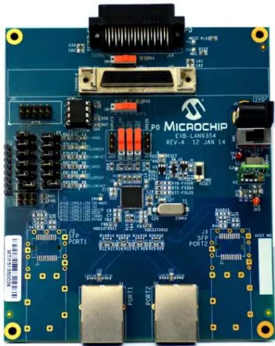
A.1 INTRODUCTION
This appendix shows the EVB-LAN9354 Evaluation Board.
FIGURE A-1: EVB-LAN9354 EVALUATION BOARD
text_image
P0 H220 M100 C60 S70 P0 MICROCHIP EVB-LAN9354 REV-A 12 JAN 14 S70 P0 S70 P0 SFP PORT1 SFP PORT2 Switch-68 PORT1 PORT2 ASYR M2Appendix B. EVB-LAN9354 Evaluation Board Schematics
B.1 INTRODUCTION
This appendix shows the EVB-LAN9354 Evaluation Board Schematics.
FIGURE B-1: EVB-LAN9354 EVALUATION BOARD SCHEMATIC 1
EVB-LAN9354 Block Diagram

flowchart
graph TD
    A["40 Pin MII Connector (Female)"] -->|RMII| B["Port 0"]
    C["40 Pin MII Connector (Male)"] -->|RMII| B
    D["Mode Switch"] --> B
    E["I2C EEPROM Header"] --> B
    F["Straps Jumpers"] --> B
    G["Fiber Trasnceiver-(SFP) Port 1"] --> B
    H["10/100 Ethernet Magnetics & RJ45"] --> B
    I["10/100 Ethernet Magnetics & RJ45"] --> B
    J["Fiber Trasnceiver-(SFP) Port 2"] --> B
    K["Power Supply Module"] --> B
    L["Reset Switch"] --> B
    M["Crystal"] --> B
    B --> N["Port 1 Port 2"]
FIGURE B-2: EVB-LAN9354 EVALUATION BOARD SCHEMATIC 2
text_image
POWER SUPPLY 3.1 V REFETTL A70B_3A (3V3 fixed when Rx 470Ω) U1 VOUT 5V5 2V R1 R2 R3 R4 R5 R6 R7 R8 R9 R10 R11 R12 R13 R14 R15 R16 R17 R18 R19 R20 R21 R22 R23 R24 R25 R26 R27 R28 R29 R30 R31 R32 R33 R34 R35 R36 R37 R38 R39 R40 R41 R42 R43 R44 R45 R46 R47 R48 R49 R50 R51 R52 R53 R54 R55 R56 R57 R58 R59 R60 R61 R62 R63 R64 R65 R66 R67 R68 R69 R70 R71 R72 R73 R74 R75 R76 R77 R78 R79 R80 R81 R82 R83 R84 R85 R86 R87 R88 R89 R90 R91 R92 R93 R94 R95 R96 R97 R98 R99 Reset GeneratorFIGURE B-3: EVB-LAN9354 EVALUATION BOARD SCHEMATIC 3
text_image
2VS FE2 2AC/SDCR L1 1.0F DM FE2 2AC/SDCR L2 1.0F DM FE2 2AC/SDCR L3 1.0F DM FE2 2AC/SDCR L4 1.0F DM FE2 2AC/SDCR L5 1.0F DM FE2 2AC/SDCR L6 1.0F DM FE2 2AC/SDCR L7 1.0F DM FE2 2AC/SDCR L8 1.0F DM FE2 2AC/SDCR L9 1.0F DM FE2 2AC/SDCR L10 1.0F DM FE2 2AC/SDCR L11 1.0F DM FE2 2AC/SDCR L12 1.0F DM FE2 2AC/SDCR L13 1.0F DM FE2 2AC/SDCR L14 1.0F DM FE2 2AC/SDCR L15 1.0F DM FE2 2AC/SDCR L16 1.0F DM FE2 2AC/SDCR L17 1.0F DM FE2 2AC/SDCR L18 1.0F DM FE2 2AC/SDCR L19 1.0F DM FE2 2AC/SDCR L20 1.0F DM FE2 2AC/SDCR L21 1.0F DM FE2 2AC/SDCR L22 1.0F DM FE2 2AC/SDCR L23 1.0F DM FE2 2AC/SDCR L24 1.0F DM FE2 2AC/SDCR L25 1.0F DM FE2 2AC/SDCR L26 1.0F DM FE2 2AC/SDCR L27 1.0F DM FE2 2AC/SDCR L28 1.0F DM FE2 2AC/SDCR L29 1.0F DM FE2 2AC/SDCR L30 1.0F DM FE2 2AC/SDCR L31 1.0F DM FE2 2AC/SDCR L32 1.0F DM FE2 2AC/SDCR L33 1.0F DM FE2 2AC/SDCR L34 1.0F DM FE2 2AC/SDCR L35 1.0F DM FE2 2AC/SDCRFIGURE B-4: EVB-LAN9354 EVALUATION BOARD SCHEMATIC 4

text_image
PORT1 SODOS/RRX1 FBG 0E R1 40.9 120A 1% R12 45.3 120A 1% R13 49.9 120A 1% R-4 110A 1% R15 5E TIPAC(21P) TINAC(21P) FX_SFP_TIF4 FX_SFP_TINAC FX_SFP-XCPA FX_SFP-XCPA FX_SFP-XCPA TXP TXN TXNAC TXN TXNAC TXN TXN TXN TXN TXN TXN TXN TXN TXN TXN TXN TXN TXN TXN TXN TXN TXN TXN TXN TXN TXN TXN TXN TXN TXN TXN TXN TXN TXN TXN TXN TXN TXN TXN
text_image
PORT2 VDC607X49X2 T1F2 R25 47.8 10kV 1% R26 45.3 10kV 1% R27 45.0 10kV 1% R28 38.9 10kV 1% R29 TE INM04CT LED5 CATHODES T2 Pure JCM1001ENL TXMT TXCT TE 1 4 & 5 2 3 7 & 8 6 LED Player = UMC001 LED Drive* SWEEL TXM NC CHD OND GND GND KNT5 KNT51 YEL SWEEL SWEEL (LED3 A00E) RES1210 SPEEDFIGURE B-5: EVB-LAN9354 EVALUATION BOARD SCHEMATIC 5

text_image
Fiber Port 2 :SFP Interface Assemble OE at C29,C41,C43,C45 Note Place capacitors, and resistors close to FDT C90 10.1uF C47 10.1uF C23 10.1uF C68 10.1uF R51 10.1uF R52 10.1uF Note Place resistors close to ASIC SFP VCC72 SFP VCC82 L1 1uH C61 0.1uF C52 10kV L3 1uH C37 0.1uF J5 FTLP12/TP2 SFP VCC73 R57 4.7K R58 4.7K R59 4.7K R60 4.7K R61 10.1uF FXOS/PXLOSENote: Fiber mode related components are Not Populated on EVB (Default)
FIGURE B-6: EVB-LAN9354 EVALUATION BOARD SCHEMATIC 6
text_image
GPIO [0:5] & LED_POL_Shrap 3V3 3V3 LED1 SPAD R12 R14 R16 R18 R20 R22 R24 R26 R28 R30 R32 R34 R36 R38 R40 R42 R44 R46 R48 R50 R52 R54 R56 R58 R60 R62 R64 R66 R68 R70 R72 R74 R76 R78 R80 R82 R84 R86 R88 R90 R92 R94 R96 R98 R100 LED ANDELED CATHODE LED CANODE LED CATHODE LED CATHODE LED CANODE LED CANODE LED CANODE LED CANODE LED CANODE LED CANODE LED CANODE LED CANODE LED CANODE LED CANODE LED CANODE LED CANODE LED CANODE LED CANODE LED CANODE LED CANODE LED CANODE LED CANODE LED CANODE LED CANODE LED CANODE LED CANODE LED CANODE LED CANODE LED CANODE LED CANODE LED CANODE LED CANODE LED CANODE LED CANODE LED CANODE LED CANODE LED CANODE LED CANADELED LED ANDELED CATHODE LED CANODE LED CANODE LED CANODE LED CANODE LED CANODE LED CANODE LED CANODE LED CANODE LED CANODE LED CANODE LED CANODE LED CANODE LED CANODE LED CANODE LED CANODE LED CANODE LED CANODE LED CANODE LED CANODE LED CANODE LED CANODE LED CANODE LED CANODE LED CANODE LED CANODE LED CANODE LED CANODE LED CANODE LED CANODE LED CANODE LED CANODE LED CANODE LDHANONE LUXED ON LUXED ON LUXED ON LUXED ON LUXED ON LUXED ON LUXED ON LUXED ON LUXED ON LUXED ON LUXED ON LUXED ON LUXED ON LUXED ON LUXED ON LUXED ON LUXED ON LUXED ON LUXED ON LUXED ON LUXED ON LUXED ON LUXED ON LUXED ON LUXED ON LUXED IN LUXED ON LUXED ON LUXED ON LUXED ON LUXED ON LUXED ON LUXED ON LUXED ON LUXED ON LUXED ON LUXED ON LUXED ON LUXED ON LUXED ON LUXED ON LUXED ON LUXED ON LUXED ON LUXED ON LUXED ON LUXED ON LUXED ON LUXED ON LUXED ON LUXED OR LUXED ON LUXED ON LUXED ON LUXED ON LUXED ON LUXED ON LUXED ON LUXED ON LUXED ON LUXED ON LUXED ON LUXED ON LUXED ON LUXED ON LUXED ON LUXED ON LUXED ON LUXED ON LUXED ON LUXED ON LUXED ON LUXED ON LUXED ON LUXED ON LUXED OF THE POWER OF THE POWER OF THE POWER OF THE POWER OF THE POWER OF THE POWER OF THE POWER OF THE POWER OF THE POWER OF THE POWER OF THE POWER OF THE POWER OF THE POWER OF THE POWER OF THE POWER OF THE POWER OF THE POWER OF THE POWER OF THE POWER OF THE POWER OF THE POWER OF THE POWER OF THE POWER OF THE POWER OF THE POWER OF THE POWER OF THE POWER OF THE POWER OF THE POWER OF THE POWER OF THE POWER OF THE POWER OF THE POWER OF THE POWER of THE POWER OF THE POWER OF THE POWER OF THE POWER OF THE POWER OF THE POWER OF THE POWER OF THE POWER OF THE POWER OF THE POWER OF THE POWER OF THE POWER OF THE POWER OF THE POWER OF THE POWER OF THE POWER OF THE POWER OF THE POWER OF THE POWER OF THE POWER OF THE POWER OF THE POWER OF THE POWER OF THE POWER OF THE POWER OF THE POWER OF THE POWER OF THE POWER OF THE POWER OF THE POWER OF THE POWER OF THE POWER OF THE POWER OF The POWER OF THE POWER OF THE POWER OF THE POWER OF THE POWER OF THE POWER OF THE POWER OF THE POWER OF THE POWER OF THE POWER OF THE POWER OF THE POWER OF THE POWER OF THE POWER OF THE POWER OF THE POWER OF THE POWER OF THE POWER OF THE POWER OF THE POWER OF THE POWER OF THE POWER OF THE POWER OF THE POWER OF THE POWER OF THE POWER OF THE POWER OF THE POWER OF THE POWER OF THE POWER OF THE POWER OF THE POWER OF THE POWER OF THE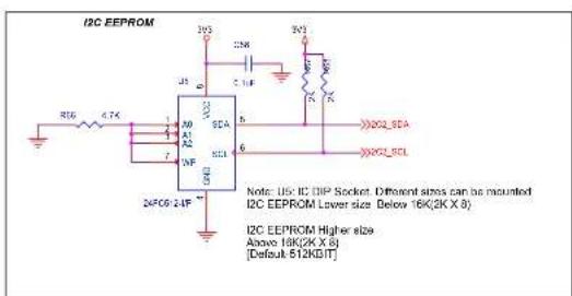
text_image
I2C EEPROM R16 4.7K A0 SE4 A1 SE4 A2 INF 24F09-2.4F 3V5 CONR 3V3 U5 U6 U7 U8 U9 U10 U11 U12 U13 U14 U15 U16 U17 U18 U19 U20_SEA U21_SCL Note: US: IC DIP Socket. Different sizes can be mounted I2C EEPROM Lower size Below 16K(2K X 8) I2C EEPROM Higher size Above 16K(2K X 8) [Default 512KBIT]
text_image
FX_Los_Srap_1 & 2 FXT IP70 Net Voltage F13200 Populations lead 201 (Amount 2 V from FX-05 for pin 1 now) Populations Populations P5 Line of 1.5V to 2.5V FX-05 for pin 1 and 1.5V copper loaded pair for pin 2 Lumber determined by FX364. DIF (Default) 0 (Default) (0.5bit) Line of 0.5V from FX-05 to copper loaded pair for pin 2 and 1 Author determined by FX364 and FX368. AET-SIPAL CHINA FX_Los_Srap_1& 2 303 12V (3K) (3M) 470 (3K)
text_image
FX_Mode_Strap_1 & 2 FOSL DRIP 10K FOSL 10K DRIP 10K FOSL 10K FOSL 10K FOSL 10K FOSL 10K FOSL 10K FOSL 10K FOSL 10K FOSL 10K FOSL 10K FOSL 10K FOSL 10K FOSL 10K FOSL 10k FOSL 10k FOSL 10k FOSL 10k FOSL 10k FOSL 10k FOSL 10k FOSL 10k FOSL 10k FOSL 10k FOSL 10k FOSL 10k FOSL 10k FOS L FOS L FOS L FOS L FOS L FOS L FOS L FOS L FOS L FOS L FOS L FOS L FOS L FOS L FOS L FOS L FOS L FOS L FOS L FOS L FOS L FOS L FOS L FOS L FOS L FOS M FOS M FOS M FOS M FOS M FOS M FOS M FOS M FOS M FOS M FOS M FOS M FOS M FOS M FOS M FOS M FOS M FOS M FOS M FOS M FOS M FOS M FOS M FOS M FOS M FOS N FOS N FOS N FOS N FOS N FOS N FOS N FOS N FOS N FOS N FOS N FOS N FOS N FOS N FOS N FOS N FOS N FOS N FOS N FOS N FOS NFIGURE B-7: EVB-LAN9354 EVALUATION BOARD SCHEMATIC 7
Emulated Link Partner Default Advertised Ability for Port 0
| ISO(PE_SUB-13) | ISO(PE_APPD) | DegreeGroup# | SpeedGroup# | NOMOTENED LINE PARTNERS PABLEF(SHAAT 27.5) |
| 1.2 | 2.1 | - | 4 | 100% - 8.8 kg (SHE) |
| 1.2.1.2 | - | + | 100% - 8.8 kg (100% - DHA) | |
| 2.1.1.2 | 2 | 9 | 100% - 8.8 kg (100%) | |
| 3.5 | 1.2 | 4 | - | 100% - 8.8 kg (100%) |

| Port 0 Mode string Tagging | |||
| P0/NODES (50%) | P0/NODES (50%) | P0/NODES (50%) | MODES |
| 0 | 0 | 0 | RUT1 NAGE button |
| Short 1-2.5 | Short 1-2.5 | ||
| 0 | 1 | 0 | RUT1 NAGE button and 17ms |
| Short 1-2.5 | Short 1-2.5 | 2 | |
| 0 | 1 | 1 | RUT1 NAGE button and 18ms (fixed) |
| Short 1-2.5 | Short 1-2.5 | 2 | RUT1 NAGE button |
| 0 | 0 | 0 | |
| Short 1-2.5 | Short 1-2.5 | ||
| 1 | 1 | 0 | RUT1 Short 1-2.5 and 18ms |
| Short 1-2.5 | Short 1-2.5 | 2 | |
| 1 | 1 | 1 | RUT1 Short 1-2.5 and 18ms |
| Short 1-2.5 | Short 1-2.5 | 2 | |
Note: For Services to share 1-3, which function should be at 1-2 and write value

text_image
Aardvark - I2C Connector 1 2 3 4 5 6 7 8 9 10 11 12 13 14 15 16 17 18 19 20 21 22 23 24 25 26 27 28 29 30 31 32 33 34 35 36 37 38 39 40 41 42 43 44 45 46 47 48 49 49.1 50 50.1.2x 51 51.2x 52 52.2x 53 53.2x 54 54.2x 55 55.2x 56 56.2x 57 57.2x 58 58.2x 59 59.2x 60 60.2x 61 61.2x 62 62.2x 63 63.2x 64 64.2x 65 65.2x 66 66.2x 67 67.2x 68 68.2x 69 69.2x 70 70.2x 71 71.2x 72 72.2x 73 73.2x 74 74.2x 75 75.2x 76 76.2x 77 77.2x 78 78.2x 79 79.2x 80 80.2x 81 81.2x 82 82.2x 83 83.2x 84 84.2x 85 85.2x 86 86.2x 87 87.2x 88 88.2x 89 89.2x 90 90.2x 91 91.2x 92 92.2x 93 93.2x 94 94.2x 95 95.2x 96 96.2x 97 97.2x 98 98.2x 99 99.2xPullup for MDIO(common for all PHY) signal
Appendix C. Bill of Materials (BOM)
C.1 INTRODUCTION
This appendix includes the EVB-LAN9354 Evaluation Board Bill of Materials (BOM).
Configuration: Two internal copper mode with higher size EEPROM (24FC512)
TABLE C-1: EVB-LAN9354 EVALUATION BOARD BILL OF MATERIALS
| Item | Qty | Reference | Designator(s) Part PCB Footprint Manufacturer | Manufacturer Manufacturer Part Number | |||
| 1 2 | C2,C4 | 10uF | CAP0805 Murata GRM21BR61E106KA73L | ||||
| 2 19 | C3,C5,C6,C8 | C10,C11,C13,C14,C15,C16,C17,C18,C21,C22,C24,C25,C58,C60,C62 | 0.1uF | CAP0603 Murata GRM155R61E104KA7D | |||
| 3 1 | C19 | 1uF | CAP0603 Murata GRM188R61C105KA93D | ||||
| 4 1 | C20 | 470pF | CAP0603 Murata GRM033R71E471KA01D | ||||
| 5 2 | C26,C27 | 18pF CAP0603 Murata GRM1885C1H180JA01D | |||||
| 6 2 | C32,C37 | 0.022uF | CAP0603 Kernel C0603C223K5RACTU | ||||
| 7 2 | C59,C61 | 10uF CAP0603 TDK | C1608X5R0J106K080AB | ||||
| 8 | 3 | D1,D4,D7 | GRN | LED0603 | Wurth electronics | 150 060 GS7 500 0 | |
| 9 | 1 | D2 | RED | LED0603 | Wurth electronics | 150 060 RS7 500 0 | |
| 10 5 | FB1,FB2,FB3,FB4,FB5 | 2AV0.05DCR | RES0603 Murata BLM18EG221SN1D | ||||
| 11 1 | J1 | SKT_P- | WR_2R0mm_4A_THRU_RA | th_conn_pwrjack_dc-210_rt | Cui Stack | PJ-002AH | |
| 12 | 16 J4,J5 | J6,J7,J8,J9,J10,J11,J12,J13,J14,J15,J16,J17,J22,J23 | HDR_1x3 TH_CONN_1X3P | FCI | 68000-103HLF | ||
| 13 | 1 | J18 | HEADER 8 | TH_CONN_1X8P | FCI | 68000-108HLF | |
| 14 1 | J19 | MII_RA | TH_CON- | N_TE-5173278_40P | TE | 5173278-2-ND | |
| 15 | 1 | J20 | FEMALE MII CONN | TH_CONN_MII-749069-4 | TE | 749069-4-ND | |
| 16 | 1 | J21 | HEADER 5X2 | th_conn_2x5p_BOX | FCI | 67997-210HLF | |
| 17 | 1 | Q1 | NDS355AN_NMOS | sot23-NDS | Fairchild | NDS355AN | |
| 18 | 7 | R1,R94,R95,R72,R73,R85,R86 | OE | RES0603 | Panasonic | ERJ-3GEY0R00V | |
| 19 | 4 | R2,R8,R74,R84 | 1K | RES0603 | Panasonic | ERJ-3GEYJ102V | |
| 20 1 | R3 | 3.30K RES0603 Yageo America | 9C06031A3301FKHFT | ||||
| 21 | 1 | R4 | 470E | RES0603 | BOURNS | CR0603-FX-4700ELF | |
| 22 | 1 | R4A | 33E | RES0603 | BOURNS | CR0603-FX-33R0ELF | |
| 23 1 | R5 | 4.75K RES0603 Panasonic | ERJ-3EKF4751V | ||||
| 24 | 7 | R6,R69,R70,R71,R81,R82,R83 | 10.0K | RES0603 | Panasonic | ERJ-3EKF1002V | |
| 25 | 1 | R7 | 100 | RES0603 | Panasonic | ERJ-3EKF1000V | |
| 26 | 1 | R9 | 2.2K | RES0603 | Panasonic | ERJ-3GEYJ222V | |
| 27 1 | R10 | 12.1K RES0603 Rohm | MCR01MZPF1202 | ||||
| 28 | 8 | R11,R12,R13,R14,R25,R26,R27,R28 | 49.9 | RES0603 | Yageo America | 9C06031A49R9FKHFT | |
TABLE C-1: EVB-LAN9354 EVALUATION BOARD BILL OF MATERIALS (CONTINUED)
| Item | Qty | Reference Designator(s) | Part | PCB Footprint | Manufacturer | Manufacturer Part Number |
| 29 4 | R15,R29, FB6,FB7 0E RES0603 Panasonic ERJ-3GEY0R00V | |||||
| 30 8 | R17,R19,R21,R23,R31,R33,R35,R37 0E RES0402 Panasonic ERJ-2GE0R00X | |||||
| 31 2 | R24,R38 0E RES1210 Vishay CRCW12100000Z0EA | |||||
| 32 4 | R61,R62,R63,R64 330E RES0603 Panasonic ERJ-3GEYJ331V | |||||
| 33 2 | R67,R68 2K RES0603 Panasonic ERJ-3GEYJ202V | |||||
| 34 12 | R76,R79,R80,R87,R88,R96,R97,R98,R99,R100,R102,R103 | 10K RES0603 Panasonic ERJ-3EKF1002V | ||||
| 35 | 5 | R89,R90,R91,R92,R93 | 33 | RES0603 | BOURNS | CR0603-FX-33R0ELF |
| 36 1 | R101 | 1.5K | RES0603 Panasonic ERJ-3GEYJ152V | |||
| 37 | 1 | SW1 | SW-SPDT-SLIDE | sw_ck_1101m2s3cqe2 | C&K | 1101M2S3CQE2 |
| 38 | 1 | SW2 | sw_pb_2P | sw_pb_2P | Panasonic | EVQ-PJU04K |
| 39 | 5 | SW3,SW4,SW5,SW6,SW7 | JS102011CQN | TH_SW_SPST_3P_10x2p5 | Wurth electronics | 450301014042 |
| 40 | 1 | TP1 | RED | TH_TP_60D40 | Keystone | 5000 |
| 41 | 1 | TP2 | ORANGE | TH_TP_60D40 | Keystone | 5003 |
| 42 | 2 | T1,T2 | Pulse - J0011D01BNL | thconn_pulse_rj45_j0026 | Pulse Electronics | 553-1483-ND |
| 43 1 | U1 | 3_Amp | TH_DC-DC_VERT_5PIN_P67 | M urata | OKR-T/3-W12-C | |
| 44 | 1 | U2 | TPS3125 | SOT23_5 | TI | TPS3125L30DBVR |
| 45 | 1 | U3 | 74LVC1G14 | SOT23_5 | TI | SN74LVC1G14DCKR |
| 46 | 1 | U4 | LAN9354_QFN56 | IC_QFN56_8X8MM | Microchip | LAN9354 |
| 47 | 1 | U5 | IC Base | IC_DIP8_300 | Assmann WSW Components | AR08-HZL-TT-R |
| 48 | 1 | U5 | 24C512 | IC_DIP8_300 | Microchip | 24FC512-I/P |
| 49 | 1 | Y1 | 25.000MHz | XTAL_HCM49 | Cardinal Components Inc. | CSM1Z-A5B2C5-40-25.0D18-F |
NOTES:
Worldwide Sales and Service
AMERICAS
Corporate Office
2355 West Chandler Blvd.
Chandler, AZ 85224-6199
Tel: 480-792-7200
Fax: 480-792-7277
Technical Support:
http://www.microchip.com/
support
Web Address:
www.microchip.com
Atlanta
Duluth, GA
Tel: 678-957-9614
Fax: 678-957-1455
Austin, TX
Tel: 512-257-3370
Boston
Westborough, MA
Tel: 774-760-0087
Fax: 774-760-0088
Chicago
Itasca, IL
Tel: 630-285-0071
Fax: 630-285-0075
Cleveland
Independence, OH
Tel: 216-447-0464
Fax: 216-447-0643
Dallas
Addison, TX
Tel: 972-818-7423
Fax: 972-818-2924
Detroit
Novi, M
Tel: 248-848-4000
Houston, TX
Tel: 281-894-5983
Indianapolis
Noblesville, IN
Tel: 317-773-8323
Fax: 317-773-5453
Los Angeles
Mission Viejo, CA
Tel: 949-462-9523
Fax: 949-462-9608
New York, NY
Tel: 631-435-6000
San Jose, CA
Tel: 408-735-9110
Canada - Toronto
Tel: 905-673-0699
Fax: 905-673-6509
ASIA/PACIFIC
Asia Pacific Office
Suites 3707-14, 37th Floor
Tower 6, The Gateway
Harbour City, Kowloon
Hong Kong
Tel: 852-2943-5100
Fax: 852-2401-3431
Australia - Sydney
Tel: 61-2-9868-6733
Fax: 61-2-9868-6755
China - Beijing
Tel: 86-10-8569-7000
Fax: 86-10-8528-2104
China - Chengdu
Tel: 86-28-8665-5511
Fax: 86-28-8665-7889
China - Chongqing
Tel: 86-23-8980-9588
Fax: 86-23-8980-9500
China - Dongguan
Tel: 86-769-8702-9880
China - Hangzhou
Tel: 86-571-8792-8115
Fax: 86-571-8792-8116
China - Hong Kong SAR
Tel: 852-2943-5100
Fax: 852-2401-3431
China - Nanjing
Tel: 86-25-8473-2460
Fax: 86-25-8473-2470
China - Qingdao
Tel: 86-532-8502-7355
Fax: 86-532-8502-7205
China - Shanghai
Tel: 86-21-5407-5533
Fax: 86-21-5407-5066
China - Shenyang
Tel: 86-24-2334-2829
Fax: 86-24-2334-2393
China - Shenzhen
Tel: 86-755-8864-2200
Fax: 86-755-8203-1760
China - Wuhan
Tel: 86-27-5980-5300
Fax: 86-27-5980-5118
China - Xian
Tel: 86-29-8833-7252
Fax: 86-29-8833-7256
ASIA/PACIFIC
China - Xiamen
Tel: 86-592-2388138
Fax: 86-592-2388130
China - Zhuhai
Tel: 86-756-3210040
Fax: 86-756-3210049
India - Bangalore
Tel: 91-80-3090-4444
Fax: 91-80-3090-4123
India - New Delhi
Tel: 91-11-4160-8631
Fax: 91-11-4160-8632
India - Pune
Tel: 91-20-3019-1500
Japan - Osaka
Tel: 81-6-6152-7160
Fax: 81-6-6152-9310
Japan - Tokyo
Tel: 81-3-6880-3770
Fax: 81-3-6880-3771
Korea - Daegu
Tel: 82-53-744-4301
Fax: 82-53-744-4302
Korea - Seoul
Tel: 82-2-554-7200
Fax: 82-2-558-5932 or
82-2-558-5934
Malaysia - Kuala Lumpur
Tel: 60-3-6201-9857
Fax: 60-3-6201-9859
Malaysia - Penang
Tel: 60-4-227-8870
Fax: 60-4-227-4068
Philippines - Manila
Tel: 63-2-634-9065
Fax: 63-2-634-9069
Singapore
Tel: 65-6334-8870
Fax: 65-6334-8850
Taiwan - Hsin Chu
Tel: 886-3-5778-366
Fax: 886-3-5770-955
Taiwan - Kaohsiung
Tel: 886-7-213-7828
Taiwan - Taipei
Tel: 886-2-2508-8600
Fax: 886-2-2508-0102
Thailand - Bangkok
Tel: 66-2-694-1351
Fax: 66-2-694-1350
EUROPE
Austria - Wels
Tel: 43-7242-2244-39
Fax: 43-7242-2244-393
Denmark - Copenhagen
Tel: 45-4450-2828
Fax: 45-4485-2829
France - Paris
Tel: 33-1-69-53-63-20
Fax: 33-1-69-30-90-79
Germany - Dusseldorf
Tel: 49-2129-3766400
Germany - Munich
Tel: 49-89-627-144-0
Fax: 49-89-627-144-44
Germany - Pforzheim
Tel: 49-7231-424750
Italy - Milan
Tel: 39-0331-742611
Fax: 39-0331-466781
Italy - Venice
Tel: 39-049-7625286
Netherlands - Drunen
Tel: 31-416-690399
Fax: 31-416-690340
Poland - Warsaw
Tel: 48-22-3325737
Spain - Madrid
Tel: 34-91-708-08-90
Fax: 34-91-708-08-91
Sweden - Stockholm
Tel: 46-8-5090-4654
UK - Wokingham
Tel: 44-118-921-5800
Fax: 44-118-921-5820