LP211D - Unspecified TEXAS INSTRUMENTS - Free user manual and instructions
Find the device manual for free LP211D TEXAS INSTRUMENTS in PDF.

User questions about LP211D TEXAS INSTRUMENTS
0 question about this device. Answer the ones you know or ask your own.
Ask a new question about this device
Download the instructions for your Unspecified in PDF format for free! Find your manual LP211D - TEXAS INSTRUMENTS and take your electronic device back in hand. On this page are published all the documents necessary for the use of your device. LP211D by TEXAS INSTRUMENTS.
USER MANUAL LP211D TEXAS INSTRUMENTS
● Low Power Drain . . . 900 μW Typical With 5-V Supply
●Operates From ±15 V or From a Single Supply as Low as 3 V
●Output Drive Capability of 25 mA
●Emitter Output Can Swing Below Negative Supply
● Response Time ... 1.2 μs Typ
●Low Input Currents:
Offset Current ... 2 n A T y p
Bias Current ... 15 nA Typ
●Wide Common-Mode Input Range: -14.5 V to 13.5 V Using ±15-V Supply
- Offset Balancing and Strobe Capability
●Same Pinout as LM211, LM311
●Designed To Be Interchangeable With Industry-Standard LP311
LP211...D PACKAGE
LP311 ... D, P, OR PS PACKAGE
(TOP VIEW)

text_image
EMIT OUT 1 8 VCC+ IN+ 2 7 COL OUT IN- 3 6 BAL/STRB VCC- 4 5 BALANCEdescription/ordering information
The LP211 and LP311 devices are low-power versions of the industry-standard LM211 and LM311 devices. They take advantage of stable, high-value, ion-implanted resistors to perform the same function as the LM311 series, with a 30:1 reduction in power consumption, but only a 6:1 slowdown in response time. They are well suited for battery-powered applications and all other applications where fast response times are not needed. They operate over a wide range of supply voltages, from ±18 V down to a single 3-V supply with less than 300- A current drain, but are still capable of driving a 25-mA load. The LP211 and LP311 are quite easy to apply free of oscillation if ordinary precautions are taken to minimize stray coupling from the output to either input or to the trim pins. In addition, offset balancing is available to minimize input offset voltage. Strobe capability also is provided to turn off the output (regardless of the inputs) by pulling the strobe pin low.
The LP211 is characterized for operation from -25^ to 85^ . The LP311 is characterized for operation from 0^ to 70^ .
ORDERING INFORMATION
| T_A | V_IO max AT 25°C | PACKAGE^ | ORDERABLE PART NUMBER | TOP-SIDE MARKING | |
| -0°C to 70°C | 7.5 mV | PDIP (P) Tube of 50 LP311P | LP311P | ||
| SOIC (D) | Tube of 75 LP311D | LP311 | |||
| Reel of 2500 LP311DR | |||||
| SOP (PS) Reel of 2000 LP311 | 1PSR L311 | ||||
| -25°C to 85°C | 7.5 mV | SOIC (D) | Tube of 75 LP211D | LP211 | |
| Reel of 2500 LP211DR | |||||
^ Package drawings, standard packing quantities, thermal data, symbolization, and PCB design guidelines are available at www.ti.com/sc/package.
functional block diagram

text_image
BALANCE BAL/STRB IN+ IN- COL OUT EMIT OUTabsolute maximum ratings over operating free-air temperature range (unless otherwise noted) ^†
Supply voltage (see Note 1): V_CC+ 18 V
V_CC- -18 V
Differential input voltage, V_ID (see Note 2) ±30 V
Input voltage, V_I (either input, see Notes 1 and 3) ± 15 ~V
Voltage from emitter output to V_CC- 30 V
Voltage from collector output to V_CC- 40 V
Voltage from collector output to emitter output 40 V
Duration of output short circuit (see Note 4) 40 V
Package thermal impedance, _JA (see Notes 5 and 6): D package 97°C/W
P package 85°C/W
PS package 95°C/W
Operating virtual junction temperature, T_J 150°C
Storage temperature range, T_stg –65°C to 150°C
^ Stresses beyond those listed under absolute maximum ratings may cause permanent damage to the device. These are stress ratings only, and functional operation of the device at these or any other conditions beyond those indicated in the recommended operating conditions section of this specification is not implied. Exposure to absolute-maximum-rated conditions for extended periods may affect device reliability.
NOTES: 1. All voltage values, unless otherwise noted, are with respect to the midpoint between V_CC+ and V_CC- .
-
Differential input voltages are at IN+ with respect to IN−.
-
The magnitude of the input voltage must never exceed the magnitude of the supply voltage of ±15 V, whichever is less.
-
The output may be shorted to ground or to either power supply.
-
Maximum power dissipation is a function of T_J() , _JA , and T_A . The maximum allowable power dissipation at any allowable ambient temperature is P_D = (T_J() - T_A)/_JA . Operating at the absolute maximum T_J of 150°C can affect reliability.
-
The package thermal impedance is calculated in accordance with JESD 51-7.
recommended operating conditions
| MIN | MAX | UNIT | ||
| (|V_CC| ≤ 15 V) | Input voltage | V_CC- + 0.5 | V_CC+ - 1.5 | V |
| V_CC+ - V_CC- | Supply voltage | 3.5 | 30 | V |
electrical characteristics at specified free-air temperature, V_CC± = ± 15 V (unless otherwise noted)
| PARAMETER TEST CONDITIONS | S T | A | MIN TYP | † | MAX | UNIT | ||
| V_ID | Input offset voltage RS < 100 kΩ, See Note | 702-100 kΩ | 25~N=7 | 25°C 2 7.5 | mV | |||
| Full range | 10 | |||||||
| V_OL | Low-level output voltage | V_ID< -10 mV, I See Note 8 | I_OL=25 mA, | 25°C | 0.4 1.5 | V | ||
| V_CC=4.5 V,V_ID< -10 mV,V See Note 8 | V_CC-=0,I_OL^=1.6 mA, | Full range | 0.1 0.4 | V | ||||
| I_IO | Input offset current | See Note 7 | 25°C 2 | 25 | nA | |||
| Full range | 35 | |||||||
| I_IB | Input bias current | 25°C | 15 | 100 | nA | |||
| Full range | 150 | |||||||
| Low-level strobe current | V_(strobe)=0.3 V, See Note 9 | V_ID< -10 mV, | 25°C | 100 | 300 μA | ^ | ||
| I_O(off) | Output off-state current | V_ID>10 mV, | V_CE=35 V | 25°C | 0.2 | 100 | nA | |
| A_VD | Large-signal differential-voltage amplification | R_L=5 kΩ | 25°C | 40 | 100 | V/mV | ||
| I_CC+ | Supply current from V_CC+ | V_ID=-50 mV,R | L= | Full range | 150 | 300 | μA | |
| I_CC- | Supply current from V_CC- | V_ID=50 mV, | R_L= | Full range | -80 | -180 | μA | |
^ All typical values are at V_CC± = ±15 V, T_A = 25^ .
NOTES: 7. The offset voltages and offset currents given are the maximum values required to drive the output within 1V of either supply with a 1-mA load. Thus, these parameters define an error band and take into account the worst-case effects of voltage gain and input impedance.
8. Voltages are with respect to EMIT OUT and V_CC -tied together.
9. The strobe should not be shorted to ground; it should be current driven at 100 A to 300 A.
switching characteristics, V_CC± = ± 5 V, T_A = 25^ C (unless otherwise noted)
| PARAMETER | TEST CONDITIONS | TYP | UNIT |
| Response time | See Note 10 | 1.2 | s |
NOTE 10: The response time is specified for a 100-mV input step with 5-mV overdrive.
TYPICAL APPLICATION CIRCUIT
text_image
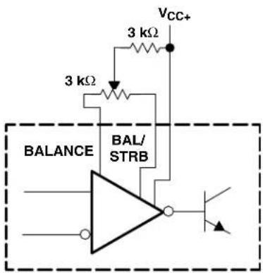
VCC+ 3 kΩ 3 kΩ BALANCE BAL/STRBNOTE: If offset balancing is not used, the BALANCE and BAL/STRB pins should be shorted together.
Figure 1. Offset Balancing

text_image
BAL/STRB TTL Strobe 2N2222 15 kΩNOTE: Do not connect strobe pin directly to ground, because the output is turned off whenever current is pulled from the strobe pin.
Figure 2. Strobing
PACKAGING INFORMATION
| Orderable Device Status(1) | Package Type | Package Drawing | Pins | Package Qty | Eco Plan(2) | Lead finish/ Ball material(6) | MSL Peak Temp(3) | Op Temp (°C) | Device Marking(4-5) | Samples | |
| LP211D ACTIVE SOIC D 8 75 RoHS & Green NIPDAU Level-1-260C-UNLIM -25 to 85 LP211 | Samples | ||||||||||
| LP211DR ACTIVE SOIC D 8 2500 RoHS & Green NIPDAU Level-1-260C-UNLIM -25 to 85 LP211 | Samples | ||||||||||
| LP211DRE4 ACTIVE SOIC D 8 2500 RoHS & Green NIPDAU Level-1-260C-UNLIM -25 to 85 LP211 | Samples | ||||||||||
| LP211DRG4 | ACTIVE SOIC D 8 2500 RoHS & Green NIPDAU Level-1-260C-UNLIM -25 to 85 LP211 | Samples | |||||||||
| LP311D ACTIVE SOIC D 8 75 RoHS & Green NIPDAU Level-1-260C-UNLIM 0 to 70 LP311 | Samples | ||||||||||
| LP311DR ACTIVE SOIC D 8 2500 RoHS & Green NIPDAU Level-1-260C-UNLIM 0 to 70 LP311 | Samples | ||||||||||
| LP311DRG4 | ACTIVE | SOIC | D | 8 | 2500 | RoHS & Green | NIPDAU | Level-1-260C-UNLIM | 0 to 70 | LP311 | Samples |
| LP311P | ACTIVE | PDIP | P | 8 | 50 | RoHS & Green | NIPDAU | N / A for Pkg Type | 0 to 70 | LP311P | Samples |
| LP311PE4 | ACTIVE | PDIP | P | 8 | 50 | RoHS & Green | NIPDAU | N / A for Pkg Type | 0 to 70 | LP311P | Samples |
(1) The marketing status values are defined as follows:
ACTIVE: Product device recommended for new designs.
LIFEBUY: TI has announced that the device will be discontinued, and a lifetime-buy period is in effect.
NRND: Not recommended for new designs. Device is in production to support existing customers, but TI does not recommend using this part in a new design.
PREVIEW: Device has been announced but is not in production. Samples may or may not be available.
OBSOLETE: TI has discontinued the production of the device.
(2) RoHS: TI defines "RoHS" to mean semiconductor products that are compliant with the current EU RoHS requirements for all 10 RoHS substances, including the requirement that RoHS substance do not exceed 0.1% by weight in homogeneous materials. Where designed to be soldered at high temperatures, "RoHS" products are suitable for use in specified lead-free processes. TI may reference these types of products as "Pb-Free".
RoHS Exempt: TI defines "RoHS Exempt" to mean products that contain lead but are compliant with EU RoHS pursuant to a specific EU RoHS exemption.
Green: TI defines "Green" to mean the content of Chlorine (Cl) and Bromine (Br) based flame retardants meet JS709B low halogen requirements of <=1000ppm threshold. Antimony trioxide based flame retardants must also meet the <=1000ppm threshold requirement.
(3) MSL, Peak Temp. - The Moisture Sensitivity Level rating according to the JEDEC industry standard classifications, and peak solder temperature.
(4) There may be additional marking, which relates to the logo, the lot trace code information, or the environmental category on the device.
(5) Multiple Device Markings will be inside parentheses. Only one Device Marking contained in parentheses and separated by a "\~" will appear on a device. If a line is indented then it is a continuation of the previous line and the two combined represent the entire Device Marking for that device.
(6) Lead finish/Ball material - Orderable Devices may have multiple material finish options. Finish options are separated by a vertical ruled line. Lead finish/Ball material values may wrap to two lines if the finish value exceeds the maximum column width.
Important Information and Disclaimer: The information provided on this page represents TI's knowledge and belief as of the date that it is provided. TI bases its knowledge and belief on information provided by third parties, and makes no representation or warranty as to the accuracy of such information. Efforts are underway to better integrate information from third parties. TI has taken and continues to take reasonable steps to provide representative and accurate information but may not have conducted destructive testing or chemical analysis on incoming materials and chemicals. TI and TI suppliers consider certain information to be proprietary, and thus CAS numbers and other limited information may not be available for release.
In no event shall TI's liability arising out of such information exceed the total purchase price of the TI part(s) at issue in this document sold by TI to Customer on an annual basis.
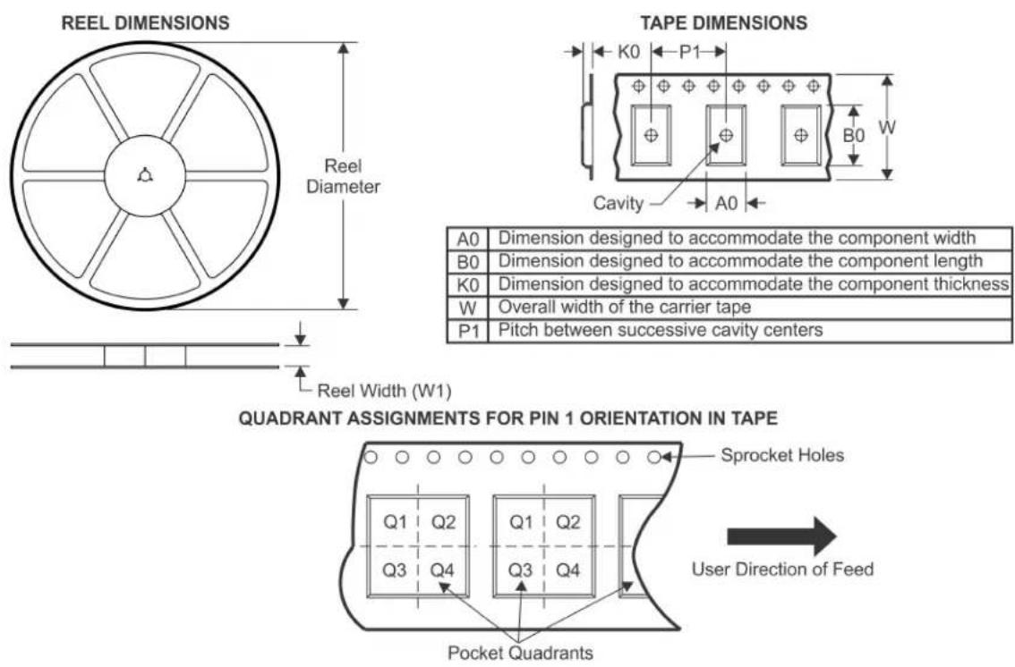
TAPE AND REEL INFORMATION
*All dimensions are nominal
| Device Package | Type | Package Drawing | Pins | SPQ Reel | Diameter (mm) | Reel Width W1 (mm) | A0 (mm) | B0 (mm) | K0 (mm) | P1 (mm) | W (mm) | Pin1 Quadrant |
| LP211DR SOIC D | 8 2500 33 | 0.0 12.4 6 | 4 5.2 | 2.1 8.0 12.0 Q1 | ||||||||
| LP311DR SOIC D | 8 2500 33 | 0.0 12.4 6 | 4 5.2 | 2.1 8.0 12.0 Q1 |
text_image
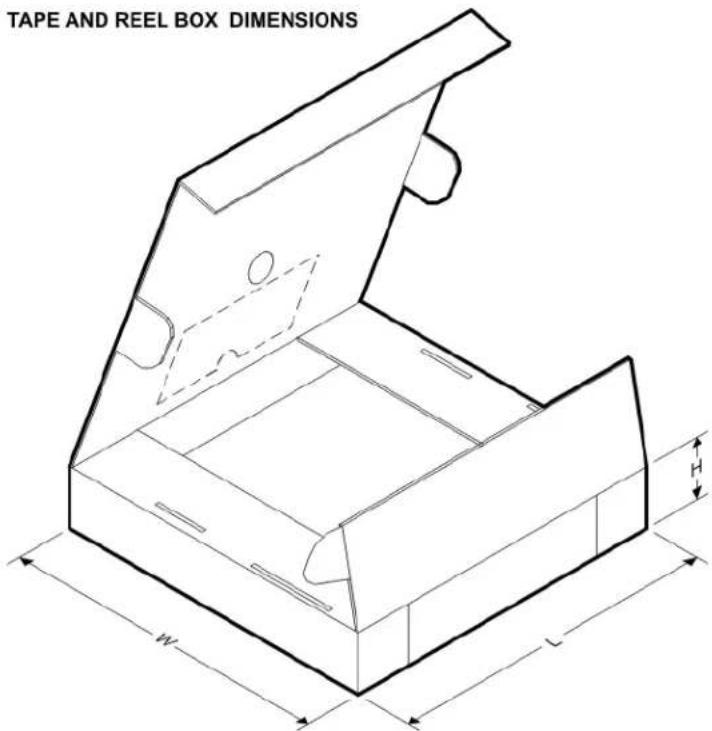
TAPE AND REEL BOX DIMENSIONS W L*All dimensions are nominal
| Device | Package Type | Package Drawing | Pins | SPQ | Length (mm) | Width (mm) | Height (mm) |
| LP211DR SOIC D | 8 2500 340.5 336.1 | 25.0 | |||||
| LP311DR SOIC D | 8 2500 340.5 336.1 | 25.0 |
TUBE

text_image
T - Tube height W-Tube width L - Tube length B - Alignment groove width*All dimensions are nominal
| Device | Package Name | Package Type | Pins | SPQ | L (mm) | W (mm) | T (μm) | B (mm) |
| LP211D D SOIC 8 | 75 507 8 3940 4.32 | |||||||
| LP311D D SOIC 8 | 75 507 8 3940 4.32 | |||||||
| LP311P P PDIP 8 | 50 506 13.97 | 11230 | 432 | |||||
| LP311PE4 | P | PDIP | 8 | 50 | 506 | 13.97 | 11230 | 4.32 |
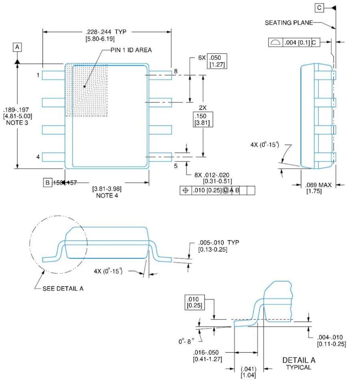
SMALL OUTLINE INTEGRATED CIRCUIT
4214825/C 02/2019
NOTES:
- Linear dimensions are in inches [millimeters]. Dimensions in parenthesis are for reference only. Controlling dimensions are in inches. Dimensioning and tolerancing per ASME Y14.5M.
- This drawing is subject to change without notice.
- This dimension does not include mold flash, protrusions, or gate burrs. Mold flash, protrusions, or gate burrs shall not exceed .006 [0.15] per side.
- This dimension does not include interlead flash.
- Reference JEDEC registration MS-012, variation AA.
SMALL OUTLINE INTEGRATED CIRCUIT
text_image
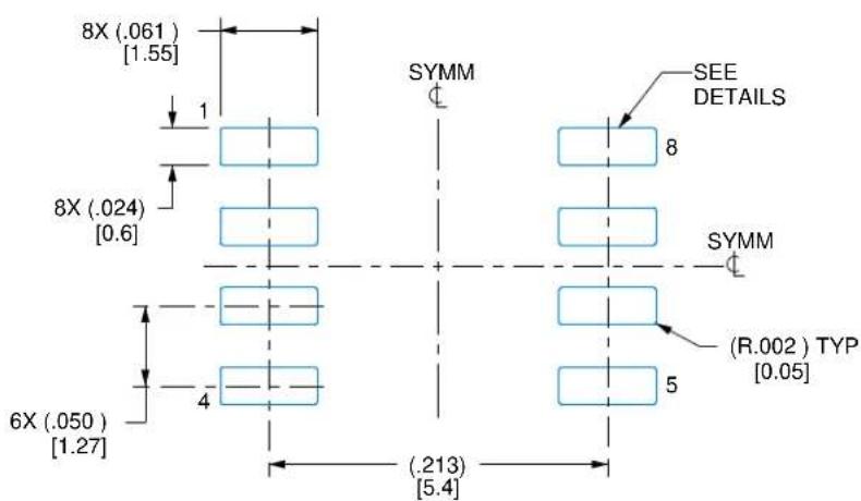
8X (.061) [1.55] 1 8X (.024) [0.6] 6X (.050) [1.27] 4 (.213) [5.4] SYMM SEE DETAILS 8 SYMM (R.002) TYP [0.05]LAND PATTERN EXAMPLE EXPOSED METAL SHOWN SCALE:8X
text_image
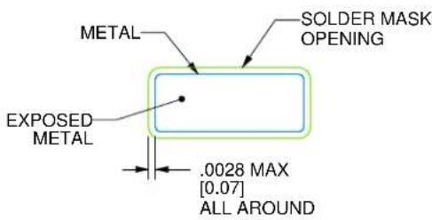
METAL SOLDER MASK OPENING EXPOSED METAL .0028 MAX [0.07] ALL AROUNDNON SOLDER MASK DEFINED
text_image
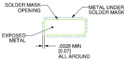
SOLDER MASK OPENING METAL UNDER SOLDER MASK EXPOSED METAL .0028 MIN [0.07] ALL AROUNDSOLDER MASK
DEFINED
SOLDER MASK DETAILS
4214825/C 02/2019
NOTES: (continued)
- Publication IPC-7351 may have alternate designs.
- Solder mask tolerances between and around signal pads can vary based on board fabrication site.
SMALL OUTLINE INTEGRATED CIRCUIT

text_image
8X (.061) [1.55] 1 8X (.024) [0.6] 6X (.050) [1.27] 4 (.213) [5.4] SYMM 8 SYMM (R.002) TYP [0.05]SOLDER PASTE EXAMPLE BASED ON .005 INCH [0.125 MM] THICK STENCIL SCALE:8X
4214825/C 02/2019
NOTES: (continued)
- Laser cutting apertures with trapezoidal walls and rounded corners may offer better paste release. IPC-7525 may have alternate design recommendations.
- Board assembly site may have different recommendations for stencil design.
P (R-PDIP-T8)
PLASTIC DUAL-IN-LINE PACKAGE

text_image
0.400 (10,16) 0.355 (9,02) 8 5 0.260 (6,60) 0.240 (6,10) 1 4 0.070 (1,78) 0.045 (1,14) 0.045 (1,14) 0.030 (0,76) 0.020 (0,51) MIN 0.200 (5,08) MAX Seating Plane 0.125 (3,18) MIN 0.100 (2,54) 0.021 (0,53) 0.015 (0,38) ⊕ 0.010 (0,25) M 0.325 (8,26) 0.300 (7,62) 0.015 (0,38) Gauge Plane 0.010 (0,25) NOM 0.430 (10,92) MAX 4040082/E 04/2010NOTES: A. All linear dimensions are in inches (millimeters).
B. This drawing is subject to change without notice.
C. Falls within JEDEC MS-001 variation BA.
IMPORTANT NOTICE AND DISCLAIMER
TI PROVIDES TECHNICAL AND RELIABILITY DATA (INCLUDING DATA SHEETS), DESIGN RESOURCES (INCLUDING REFERENCE DESIGNS), APPLICATION OR OTHER DESIGN ADVICE, WEB TOOLS, SAFETY INFORMATION, AND OTHER RESOURCES "AS IS" AND WITH ALL FAULTS, AND DISCLAIMS ALL WARRANTIES, EXPRESS AND IMPLIED, INCLUDING WITHOUT LIMITATION ANY IMPLIED WARRANTIES OF MERCHANTABILITY, FITNESS FOR A PARTICULAR PURPOSE OR NON-INFRINGEMENT OF THIRD PARTY INTELLECTUAL PROPERTY RIGHTS.
These resources are intended for skilled developers designing with TI products. You are solely responsible for (1) selecting the appropriate TI products for your application, (2) designing, validating and testing your application, and (3) ensuring your application meets applicable standards, and any other safety, security, regulatory or other requirements.
These resources are subject to change without notice. TI grants you permission to use these resources only for development of an application that uses the TI products described in the resource. Other reproduction and display of these resources is prohibited. No license is granted to any other TI intellectual property right or to any third party intellectual property right. TI disclaims responsibility for, and you will fully indemnify TI and its representatives against, any claims, damages, costs, losses, and liabilities arising out of your use of these resources.
TI's products are provided subject to TI's Terms of Sale or other applicable terms available either on ti.com or provided in conjunction with such TI products. TI's provision of these resources does not expand or otherwise alter TI's applicable warranties or warranty disclaimers for TI products.
TI objects to and rejects any additional or different terms you may have proposed.
Mailing Address: Texas Instruments, Post Office Box 655303, Dallas, Texas 75265
Copyright © 2022, Texas Instruments Incorporated