LMC6484IM/NOPB - Amplificateur opérationnel TEXAS INSTRUMENTS - Free user manual and instructions
Find the device manual for free LMC6484IM/NOPB TEXAS INSTRUMENTS in PDF.

User questions about LMC6484IM/NOPB TEXAS INSTRUMENTS
0 question about this device. Answer the ones you know or ask your own.
Ask a new question about this device
Download the instructions for your Amplificateur opérationnel in PDF format for free! Find your manual LMC6484IM/NOPB - TEXAS INSTRUMENTS and take your electronic device back in hand. On this page are published all the documents necessary for the use of your device. LMC6484IM/NOPB by TEXAS INSTRUMENTS.
USER MANUAL LMC6484IM/NOPB TEXAS INSTRUMENTS
LMC6484CMOS, Quad, Rail-to-RailInputandOutput, OperationalAmplifier
1Features
• Rail-to-railinputcommon-modevoltagerange (specified over temperature)
• Rail-to-railoutputswing(within20mVofsupply rail,100-kΩ load)
•Specified3-V,5-Vand15-Vperformance
•ExcellentCMRRandPSRR:82dB
•Ultra-lowinputcurrent:20fA
•Highvoltagegain(R _L=500k ):130dB
•Specifiedfor2-kΩ and600-Ω loads
2Applications
•Dataacquisition(DAQ)
•Currencycounter
•Oscilloscope(DSO)
• Intra-DCinterconnect(METRO)
• Macroremoteradiounit(RRU)
•Multiparameterpatientmonitor
• Merchanttelecomrectifiers
• Traincontrolandmanagement
- Processanalytics(pH,gas,concentration,force, andhumidity)
•ThreephaseUPS
- ImprovedreplacementforTLC274,TLC279
3Description
TheLMC6484deviceprovidesacommon-mode rangethatextendstobothsupplyrails. Thisrail-to-rail performancecombinedwithexcellentaccuracy, due toahighCMRR, makethisdeviceuniqueamong rail-to-railinputamplifiers.
TheLMC6484isanexcellentchoiceforsystems, suchasdataacquisition,that requirealargeinput signal range. The device is also an excellent upgrade forcircuitsusinglimitedcommon-moderange amplifiers,suchastheTLC274andTLC279.
Maximum dynamic signal range is maintained in low voltage and single-supply systems by the rail-to-rail output swing of the LMC6484. The rail-to-rail output swing of the LMC6484 is specified for loads down to 600Ω.
Specifiedlowvoltagecharacteristicsandlowpower dissipationmaketheLMC6484 an excellentchoice forbattery-operatedsystems.
See the LMC6482 for a dual CMOS operational amplifierwiththesesamefeatures.
DeviceInformation (1)
| PARTNUMBER | PACKAGE | BODYSIZE(NOM) |
| LMC6484 | SOIC(14) | 8.65mm×3.91mm |
| PDIP(14) | 19.177mm×6.35mm |
(1) For all available packages, seethe package option addendum at the end of the datasheet.
Single-EndedUnityGainBuffer

text_image
+3V 0.1 μF VIN + 1/4 LMC6484 - VOUTTableofContents
1 Features.... 1
2 Applications 1
3 Description 1
4 Revision History...... 2
5PinConfigurationandFunctions....3
6 Specifications.... 4
6.1 AbsoluteMaximumRatings....4
6.2ESDRatings....4
6.3RecommendedOperatingConditions....4
6.4ThermalInformation....4
6.5DCElectricalCharacteristicsforLMC6484AI....5
6.6DCElectricalCharacteristicsforLMC6484I....7
6.7DCElectricalCharacteristicsforLMC6484M....9
6.8DCElectricalCharacteristicsforLMC6484AI....11
6.9DCElectricalCharacteristicsforLMC6484I......11
6.10DCElectricalCharacteristicsforLMC6484M.....12
6.11ACElectricalCharacteristicsforLMC6484A....13
6.12ACElectricalCharacteristicsforLMC6484I.....13
6.13ACElectricalCharacteristicsforLMC6484M.....14
6.14ACElectricalCharacteristics:V + =3V,V - =0V.14
6.15TypicalCharacteristics....15
7DetailedDescription....23
7.1Overview....23
7.2FunctionalBlockDiagram....23
7.3FeatureDescription....23
7.4DeviceFunctionalModes....24
8ApplicationandImplementation....25
8.1 Application Information....25
8.2TypicalApplication....25
8.3SystemExamples....31
9PowerSupplyRecommendations....36
10 Layout.... 36
10.1 LayoutGuidelines....36
10.2LayoutExample....37
11DeviceandDocumentationSupport....38
11.1DeviceSupport....38
11.2DocumentationSupport....38
11.3SupportResources....38
11.4Trademarks....38
11.5ElectrostaticDischargeCaution....38
11.6Glossary....38
12Mechanical, Packaging, and Orderable Information 38
4RevisionHistory
NOTE: Pagenumbersforpreviousrevisionsmaydifferfrompagenumbersinthecurrentversion.
ChangesfromRevisionC(September2015)toRevisionDPage
- Deleted old note 3 from DC Electrical Characteristics for LMC6484AI table 5
- Deleted old note 3 from DC Electrical Characteristics for LMC6484I table 7
- Deleted old note 3 from DC Electrical Characteristics for LMC6484M table 9
ChangesfromRevisionB(August2000)toRevisionC
Page
- Added ESD Ratings table, Feature Description section, Device Functional Modes, Application and Implementation section, Power Supply Recommendations section, Layout section, Device and Documentation Support section, and Mechanical, Packaging, and Orderable Information section. 1
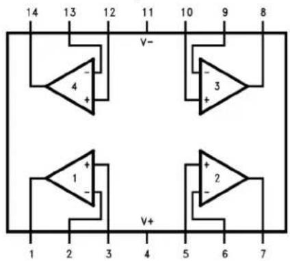
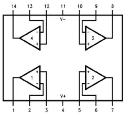
5PinConfigurationandFunctions
DorNFFPackages
14-PinSOICorPDIP
TopView
text_image
14 13 12 11 10 9 8 4 V- 3 + 1 + - 2 V+ 5 6 7 1 2 3 4 5 6 7PinFunctions
| PIN | TYPEDESCRIPTION | |
| NO.NAME | ||
| 1OUTPUT | T10OutputforAmplifier1 | |
| 2INVERT | INGINPUT1InvertinginputforAmplifier1 | |
| 3 | NONINVERTING INPUT1 | INoninvertinginputforAmplifier1 |
| 4 | V+ | P Positivevoltagesupplypin |
| 5 | NONINTERTING INPUT2 | INoninvertinginputforAmplifier2 |
| 6INVERT | INGINPUT2InvertinginputforAmplifier2 | |
| 7OUTPUT | T20OutputforAmplifier2 | |
| 8OUTPUT | T30OutputforAmplifier3 | |
| 9INVERT | INGINPUT3InvertinginputforAmplifier3 | |
| 10 | NONINVERTING INPUT3 | INoninvertinginputforAmplifier3 |
| 11 | V- | P Negativesupplyvoltagepin |
| 12 | NONINVERTING INPUT4 | INoninvertinginputforAmplifier4 |
| 13 | INVERTINGINPUT4InvertinginputforAmplifier4 | |
| 14 | OUTPUT40OutputforAmplifier5 | |
6Specifications
6.1 AbsoluteMaximumRatings
See ^(1)(2)
| MINMAXUNIT | |||
| Differentialinputvoltage±SupplyVoltage | |||
| Voltageatinput/outputpin(V) | ^- - 0.3(V ^+ )+0.3V | ||
| Supplyvoltage(V ^+ - V)16V | |||
| Currentatinputpin (3) | ±5 | mA | |
| Currentatoutputpin (4)(5) | ±30 | mA | |
| Currentatpowersupplypin | 40 | mA | |
| T_J | Junctiontemperature (6) | 150 | °C |
| T_stg | Storagetemperature, T_stg | -65 150 | °C |
(1) Stresses beyond those listed under Absolute Maximum Ratings may cause permanent damage to the device. These are stress ratings only, which do not imply functional operation of the device at these or any other conditions beyond those indicated under Recommended Operating Conditions. Exposure to absolute-maximum-rated conditions for extended periods may affect device reliability.
(2) If Military/Aerospace specified devices are required, contact the Texas Instruments Sales Office/Distributors for availability and specifications.
(3) Limiting input pincurrent is only necessary for input voltage that exceeds absolute maximum input voltage ratings.
(4) Applies to both single supply and split-supply operation. Continuous short circuit operation at elevated ambient temperature can result in exceeding the maximum allowed junction temperature of 150^ C. Output currents in excess of ±30 mA over long term may adversely affect reliability.
(5)DonotshortcircuitoutputtoV +,whenV + isgreaterthan13Vorreliabilitywillbeadverselyaffected.
(6)ThemaximumpowerdissipationisafunctionofT J() , R JA -and T A .Themaximumallowablepowerdissipationatanyambient temperatureisP D = (T_J() - )/R_J A .AllnumbersapplyforpackagessoldereddirectlyintoaPCboard.
6.2ESDRatings
| VALUE | UNIT | |||
| V_(ESD) | ElectrostaticdischargeHuman | bodymodel(HBM),perANSI/ESDA/JEDECJS-001 (1)(2) | ±2000 | V |
(1) JEDEC document JEP155 states that 500-V HBM allows safe manufacturing with a standard ESD control process. Manufacturing with lessthan500-VHBMispossiblewiththenecessaryprecautions.
(2) Human body model, 1.5-kΩ resistor in series with 100 pF. All pins rated per method 3015.6 of MIL-STD-883. This is a class 2 device rating.
6.3 Recommended Operating Conditions
overoperatingfree-airtemperaturerange(unlessotherwisenoted)
| MIN | MAX | UNIT | |||
| V+ | Supply voltage | 3 | 15.5 | V | |
| T_J | Junctiontemperature | LMC6484AM | -55 | 125 | °C |
| LMC6484AI, LMC6484I | -40 | 85 | °C | ||
6.4ThermalInformation
| THERMALMETRIC (1) | LMC6484 | UNIT | ||
| D(SOIC) | NFF(PDIP) | |||
| 14PINS | 14PINS | |||
| R_ JA | Junction-to-ambient thermal resistance | 110 | 70 | °C/W |
(1) For more information about traditional and new thermal metrics, see the Semiconductor and IC Package Thermal Metrics application report.
6.5DCElectricalCharacteristicsforLMC6484AI
unless otherwise specified, all limits specified for T J=25^,V^+=5V,V^-=0V,VCM=V_O=V^+/2,andR_L>1M
| PARAMETERTESTCONDITIONSMIN | (1) | TYP (2) | MAX (1) | UNIT | ||||
| V_OS | Inputoffsetvoltage | 0.110.75 | mV | |||||
| Atthetemperatureextremes1.35 | ||||||||
| TCV_OS | Inputoffsetvoltage averagedrift | 1μV/°C | ||||||
| I_B | Inputcurrent | 0.02 | pA | |||||
| Atthetemperatureextremes4 | ||||||||
| I_OS | Inputoffsetcurrent | 0.01 | pA | |||||
| Atthetemperatureextremes2 | ||||||||
| C_IN | Common-mode inputcapacitance | 3 | pF | |||||
| R_IN | Inputresistance | >10 | TeraΩ | |||||
| CMRR | Common-mode rejection ratio | 0V≤ V_CM ≤ 15V V^+ =15V | 70 | 82 | dB | |||
| Atthetemperature extremes | 67 | |||||||
| 0V≤ V_CM ≤ 5V V^+ =5V | 70 | 82 | dB | |||||
| Atthetemperature extremes | 67 | |||||||
| +PSRR | Positivepower supplyrejection ratio | 5V≤ V^+ ≤ 15V V^-=0V VO=2.5V | 70 | 82 | dB | |||
| Atthetemperature extremes | 67 | |||||||
| -PSRR | Negativepower supplyrejection ratio | -5V≤ V^- ≤ -15V V^+ =0V V_O=-2.5V | 70 | 82 | dB | |||
| Atthetemperature extremes | 67 | |||||||
| V_CM | Inputcommon-modevoltage range | V^+ =5Vand15VForCMRR≥ 50dB | V^--0.3 | -0.25 | V | |||
| Atthetemperature extremes | 0 | |||||||
| V^+ +0.25 | V^+ +0.3 | V | ||||||
| Atthetemperature extremes | V^+ | |||||||
| A_V | Largesignal voltagegain | R_L=2kΩ^(3) | Sourcing | 140 | 666 | V/mV | ||
| Atthe temperature extremes | 84 | |||||||
| Sinking | 35 | 75 | V/mV | |||||
| Atthe temperature extremes | 20 | |||||||
| R_L=600Ω^(3) | Sourcing | 80 | 300 | V/mV | ||||
| Atthe temperature extremes | 48 | |||||||
| Sinking | 20 | 35 | V/mV | |||||
| Atthe temperature extremes | 13 | |||||||
(1) Alllimitsarespecifiedbytestingorstatisticalanalysis.
(2) Typical values represent themost likely parametric normal.
(3) V^+=15V, V_CM=7.5V and R connected to 7.5V. Forsourcing tests, 7.5V ≤ V 0 ≤ 11.5V. Forsinking tests, 3.5V ≤ V 0 ≤ 7.5V.
DCElectricalCharacteristicsforLMC6484Al(continued)
unless otherwise specified, all limit specific for T J=25^,V^+=5V,V^-=0V,VCM=V_O=V^+/2 , and R_L>1M
| PARAMETERTESTCONDITIONSMIN | (1) TYP (2) MAX (1) | UNIT | |||
| V_O | Outputswing | V^+=5V R_L=2kΩ toV^+/2 | 4.84.9 | V | |
| Atthetemperature extremes | 4.7 | ||||
| 0.10.18 | V | ||||
| Atthetemperature extremes | 0.24 | ||||
| V^+=5V R_L=600Ω toV^+/2 | 4.54.7 | V | |||
| Atthetemperature extremes | 4.24 | ||||
| 0.30.5 | V | ||||
| Atthetemperature extremes | 0.65 | ||||
| V^+=15V R_L=2kΩ toV^+/2 | 14.414.7 | V | |||
| Atthetemperature extremes | 14.2 | ||||
| 0.160.32 | V | ||||
| Atthetemperature extremes | 0.45 | ||||
| V^+=15V R_L=600Ω toV^+/2 | 13.414.1 | V | |||
| Atthetemperature extremes | 13 | ||||
| 0.51 | V | ||||
| Atthetemperature extremes | 1.3 | ||||
| I_SC | Outputshortcircuit current V^+=5V | Sourcing, V_O=0V | 1620 | mA | |
| Atthetemperature extremes | 12 | ||||
| Sinking, V_O=5V | 1115 | mA | |||
| Atthetemperature extremes | 9.5 | ||||
| I_SC | Outputshortcircuit current V^+=15V | Sourcing, V_O=0V | 2830 | mA | |
| Atthetemperature extremes | 22 | ||||
| Sinking, V_O=12V^(4) | 3030 | mA | |||
| Atthetemperature extremes | 24 | ||||
| I_S | Supplycurrent | Allfouramplifiers V^+=+5V,V_O=V^+/2 | 22.8 | mA | |
| Atthetemperature extremes | 3.6 | ||||
| Allfouramplifiers V^+=+15V,V_O=V^+/2 | 2.63 | mA | |||
| Atthetemperature extremes | 3.8 | ||||
(4)WhenV ^+ isgreaterthan13V,donotshortcircuitoutputtoV ^+ orreliabilitywillbeadverselyaffected.
6.6DCElectricalCharacteristicsforLMC6484I
unless otherwise specified, all limits specified for T J=25^,V^+=5V,V^-=0V,VCM=V_O=V^+/2,andR_L>1M
| PARAMETERTESTCONDITIONS MIN | (1) | TYP(2) | MAX(1) | UNIT | ||||
| V_OS | Inputoffsetvoltage | 0.113 | mV | |||||
| Atthetemperatureextremes3.7 | ||||||||
| TCV_OS | Inputoffsetvoltage averagedrift | 1μV/°C | ||||||
| I_B | Inputcurrent | 0.02 | pA | |||||
| Atthetemperatureextremes4 | ||||||||
| I_OS | Inputoffsetcurrent | 0.01 | pA | |||||
| Atthetemperatureextremes2 | ||||||||
| C_IN | Common-mode inputcapacitance | 3 | pF | |||||
| R_IN | Inputresistance | >10 | TeraΩ | |||||
| CMRR | Common-mode rejectionratio | 0V≤ V_CM ≤ 15V V^+ =15V | 65 | 82 | dB | |||
| Atthetemperatureextremes | 62 | |||||||
| 0V≤ V_CM ≤ 5V V^+ =5V | 65 | 82 | dB | |||||
| Atthetemperatureextremes | 60 | |||||||
| +PSRR | Positivepower supplyrejectionratio | 5V≤ V^+ ≤ 15V V^-=0V,V_o=2.5V | 65 | 82 | dB | |||
| Atthetemperatureextremes | 62 | |||||||
| -PSRR | Negativepower supplyrejectionratio | -5V≤ V^- ≤ -15V V^+ =0V, V_o =-2.5V | 65 | 82 | dB | |||
| Atthetemperatureextremes | 62 | |||||||
| V_CM | Inputcommon-mode voltage range | V^+ =5Vand15VForCMRR≥ 50dB | V^- - 0.3 | -0.25 | V | |||
| Atthetemperatureextremes | 0 | |||||||
| V^+ +0.25 | V^+ +0.3 | V | ||||||
| Atthetemperatureextremes | V^+ | |||||||
| A_V | Largesignalvoltage gain | R_L=2kΩ^(3) | Sourcing | 120 | 666 | V/mV | ||
| Atthe temperature extremes | 72 | |||||||
| Sinking | 35 | 75 | ||||||
| Atthe temperature extremes | 20 | |||||||
| R_L=600Ω^(3) | Sourcing | 50 | 300 | |||||
| Atthe temperature extremes | 30 | |||||||
| Sinking | 15 | 35 | ||||||
| Atthe temperature extremes | 10 | |||||||
(1) Alllimitsarespecifiedbytestingorstatisticalanalysis.
(2) Typical values represent themost likely parametric normal.
(3) V^+=15V, V_CM=7.5V and R connected to 7.5V. Forsourcing tests, 7.5V ≤ V 0 ≤ 11.5V. Forsinking tests, 3.5V ≤ V 0 ≤ 7.5V.
DCElectricalCharacteristicsforLMC6484I(continued)
unless otherwise specified, all limit specific for T J=25^,V^+=5V,V^-=0V,VCM=V_O=V^+/2,andR_L>1M
| PARAMETERTESTCONDITIONSMIN | (1) | TYP(2) | MAX(1) | UNIT | |||
| V_O | Outputswing | V^+=5V R_L=2kΩ toV^+/2 | 4.84.9 | V | |||
| Athetemperatureextremes4.7 | |||||||
| 0.10.18 | V | ||||||
| Athetemperatureextremes0.24 | |||||||
| V^+=5V R_L=600Ω toV^+/2 | 4.54.7 | V | |||||
| Athetemperatureextremes4.24 | |||||||
| 0.30.5 | V | ||||||
| Athetemperatureextremes0.65 | |||||||
| V^+=15V R_L=2kΩ toV^+/2 | 14.414.7 | V | |||||
| Athetemperatureextremes14.2 | |||||||
| 0.160.32 | V | ||||||
| Athetemperatureextremes0.45 | |||||||
| V^+=15V R_L=600Ω toV^+/2 | 13.414.1 | V | |||||
| Athetemperatureextremes13 | |||||||
| 0.5 | 1 | V | |||||
| Athetemperatureextremes | 1.3 | ||||||
| I_SC | Outputshortcircuit current V^+=5V | Sourcing, V_O=0V | 16 | 20 | mA | ||
| Athetemperatureextremes12 | |||||||
| Sinking, V_O=5V | 11 | 15 | mA | ||||
| Athetemperatureextremes9.5 | |||||||
| I_SC | Outputshortcircuit current V^+=15V | Sourcing, V_O=0V | 28 | 30 | mA | ||
| Athetemperatureextremes22 | |||||||
| Sinking, V_O=12V^(4) | 30 | 30 | mA | ||||
| Athetemperatureextremes24 | |||||||
| I_S | Supplycurrent | Allfouramplifiers V^+=+5V V_O=V^+/2 | 22.8 | mA | |||
| Athetemperatureextremes | 3.6 | ||||||
| Allfouramplifiers V^+=+15V V_O=V^+/2 | 2.6 | 3 | mA | ||||
| Athetemperatureextremes | 3.8 | ||||||
(4)WhenV ^+ isgreaterthan13V,donotshortcircuitoutputtoV ^+ orreliabilitywillbeadverselyaffected.
6.7DCElectricalCharacteristicsforLMC6484M
unless otherwise specified, all limits specified for T J=25^,V^+=5V,V^-=0V,VCM=V_O=V^+/2,andR_L>1M
| PARAMETERTESTCONDITIONSMIN | (1) | TYP(2) | MAX(1) | UNIT | ||||
| V_OS | Inputoffsetvoltage | 0.113 | mV | |||||
| Atthetemperatureextremes3.8 | ||||||||
| TCV_OS | Inputoffsetvoltage averagedrift | 1μV/°C | ||||||
| I_B | Inputcurrent | 0.02 | pA | |||||
| Atthetemperatureextremes100 | ||||||||
| I_OS | Inputoffsetcurrent | 0.01 | pA | |||||
| Atthetemperatureextremes50 | ||||||||
| C_IN | Common-mode inputcapacitance | 3 | pF | |||||
| R_IN | Inputresistance | >10 | TeraΩ | |||||
| CMRR | Common-mode rejectionratio | 0V≤ V_CM ≤ 15V V^+ =15V | 65 | 82 | dB | |||
| Atthetemperatureextremes | 60 | |||||||
| 0V≤ V_CM ≤ 5V V^+ =5V | 65 | 8 | dB | |||||
| Atthetemperatureextremes | 60 | |||||||
| +PSRR | Positivepower supplyrejectionratio | 5V≤ V^+ ≤ 15V V^- =0V, V_O =2.5V | 65 | 82 | dB | |||
| Atthetemperatureextremes | 60 | |||||||
| -PSRR | Negativepower supplyrejectionratio | -5V≤ V^- ≤ -15V V^+ =0V V_O =-2.5V | 65 | 82 | dB | |||
| Atthetemperatureextremes | 60 | |||||||
| V_CM | Inputcommon-mode voltage range | V^+ =5Vand15VForCMRR≥ 50dB | V^- -0.3 | -0.25 | V | |||
| Atthetemperatureextremes | 0 | |||||||
| V^+ +0.25 | V^+ +0.3 | V | ||||||
| Atthetemperatureextremes | V^+ | |||||||
| A_V | Largesignalvoltage gain | R_L=2kΩ^(3) | Sourcing | 120 | 666 | V/mV | ||
| Atthe temperature extremes | 72 | |||||||
| Sinking | 35 | 75 | ||||||
| Atthe temperature extremes | 20 | |||||||
| R_L=600Ω^(3) | Sourcing | 50 | 300 | |||||
| Atthe temperature extremes | 30 | |||||||
| Sinking | 15 | 35 | ||||||
| Atthe temperature extremes | 10 | |||||||
(1) Alllimitsarespecifiedbytestingorstatisticalanalysis.
(2) Typical values represent themost likely parametric normal.
(3) V^+=15V, V_CM=7.5V and R connected to 7.5V. Forsourcing tests, 7.5V ≤ V 0 ≤ 11.5V. Forsinking tests, 3.5V ≤ V 0 ≤ 7.5V.
DCElectricalCharacteristicsforLMC6484M(continued)
unless otherwise specified, all limit specific for T J=25^,V^+=5V,V^-=0V,VCM=V_O=V^+/2 , and R_L>1M
| PARAMETERTESTCONDITIONS MIN | (1) | TYP(2) | MAX(1) | UNIT | |||
| V_O | Outputswing | V^+=5V R_L=2kΩ to V^+/2 | 4.84.9 | V | |||
| Athetemperatureextremes4.7 | |||||||
| 0.10.18 | V | ||||||
| Athetemperatureextremes0.24 | |||||||
| V^+=5V R_L=600Ω to V^+/2 | 4.54.7 | V | |||||
| Athetemperatureextremes4.24 | |||||||
| 0.30.5 | V | ||||||
| Athetemperatureextremes0.65 | |||||||
| V^+=15V R_L=2kΩ to V^+/2 | 14.414.7 | V | |||||
| Athetemperatureextremes14.2 | |||||||
| 0.160.32 | V | ||||||
| Athetemperatureextremes0.45 | |||||||
| V^+=15V R_L=600Ω to V^+/2 | 13.414.1 | V | |||||
| Athetemperatureextremes13 | |||||||
| 0.5 | 1 | V | |||||
| Athetemperatureextremes | 1.3 | ||||||
| I_SC | Outputshortcircuit current V^+=5V | Sourcing, V_O=0V | 16 | 20 | mA | ||
| Athetemperatureextremes10 | |||||||
| Sinking, V_O=5V | 11 | 15 | mA | ||||
| Athetemperatureextremes | 8 | ||||||
| I_SC | Outputshortcircuit current V^+=15V | Sourcing, V_O=0V | 28 | 30 | mA | ||
| Athetemperatureextremes20 | |||||||
| Sinking, V_O=12V^(4) | 30 | 30 | mA | ||||
| Athetemperatureextremes22 | |||||||
| I_S | Supplycurrent | Allfouramplifiers V^+=+5V V_O=V^+/2 | 22.8 | mA | |||
| Athetemperatureextremes | 3.8 | ||||||
| Allfouramplifiers V^+=+15V , V_O=V^+/2 | 2.6 | 3 | mA | ||||
| Athetemperatureextremes | 4 | ||||||
(4)WhenV ^+ isgreaterthan13V,donotshortcircuitoutputtoV ^+ orreliabilitywillbeadverselyaffected.
6.8DCElectricalCharacteristicsforLMC6484AI
unless otherwise specified, all limit specified for T J=25^,V^+=3V,V^-=0V,VCM=V_O=V^+/2,andR_L>1M
| PARAMETERTESTCONDITIONS | NSMIN | (1) | TYP (2) | MAX (1) | UNIT | ||
| V_OS | Inputoffsetvoltage | 0.92 | mV | ||||
| Atthetemperatureextremes2.7 | |||||||
| TCV_OS | Inputoffsetvoltageaveragedrift2μV/°C | ||||||
| I_B | Inputbiascurrent0.02 | pA | |||||
| I_OS | Inputoffsetcurrent | 0.01 | pA | ||||
| CMRR | Common-moderejectionratio | 0V≤ V_CM ≤ 3V | 64 | 74 | dB | ||
| PSRR | Powersupplyrejectionratio | 3V≤ V^+ ≤ 15V, V^- =0V | 68 | 80 | dB | ||
| V_CM | Inputcommon-modevoltagerange | ForCMRR≥ 50dB | V^- - 0.25 | 0 V | |||
| V^+ | V^+ +0.25 | V | |||||
| V_O | Outputswing | R_L =2kΩ to V^+/2 | 2.8 | V | |||
| 0.2 | V | ||||||
| R_L =600Ω to V^+/2 | 2.5 | 2.7 | V | ||||
| 0.37 | 0.6 | V | |||||
| I_S | Supplycurrent | Allfour amplifiers | 1.65 | 2.5 | mA | ||
| Atthetemperature extremes | 3 | ||||||
(1) Alllimitsarespecifiedbytestingorstatisticalanalysis.
(2) Typical values represent themost likely parametric normal.
6.9DCElectricalCharacteristicsforLMC6484I
unless otherwise specified, all limit specified for T J = 25^, V^+ = 3V, V^- = 0V, VCM = V_O = V^+/2, and R_L > 1M
| PARAMETER | TESTCONDITIONS | MIN (1) | TYP(2) | MAX(1) | UNIT | ||
| V_OS | Inputoffsetvoltage | 0.9 | 3 | mV | |||
| Atthetemperatureextremes | 3.7 | ||||||
| TCV_OS | Input offset voltage average drift | 2 | μV/°C | ||||
| I_B | Inputbiascurrent | 0.02 | pA | ||||
| I_OS | Inputoffsetcurrent | 0.01 | pA | ||||
| CMRR | Common-moderejectionratio | 0V≤ V_CM ≤ 3V | 60 | 74 | dB | ||
| PSRR | Powersupplyrejectionratio | 3V≤ V^+ ≤ 15V, V^- =0V | 60 | 80 | dB | ||
| V_CM | Inputcommon-modevoltage range | ForCMRR≥ 50dB | V^- - 0.25 | V | |||
| V^+ | V^+ +0.25 | V | |||||
| V_O | Outputswing | R_L =2kΩ to V^+/2 | 2.8 | V | |||
| 0.2 | V | ||||||
| R_L =600Ω to V^+/2 | 2.5 | 2.7 | V | ||||
| 0.37 | 0.6 | V | |||||
| I_S | Supplycurrent | Allfouramplifiers | 1.65 | 2.5 | mA | ||
| Atthetemperature extremes | 3 | ||||||
(1) Alllimitsarespecifiedbytestingorstatisticalanalysis.
(2) Typical values represent themost likely parametric normal.
6.10DCElectricalCharacteristicsforLMC6484M
unless otherwise specified, all limit specified for T J=25^,V^+=3V,V^-=0V,VCM=V_O=V^+/2,andR_L>1M
| PARAMETERTESTCONDITIONS | (1) | TYP(2) | MAX(1) | UNIT | |||
| V_OS | Inputoffsetvoltage | 0.93 | mV | ||||
| Atthetemperatureextremes3.8 | |||||||
| TCV_OS | Inputoffsetvoltageaverage drift | 2μV/°C | |||||
| I_B | Inputbiascurrent0.02pA | ||||||
| I_OS | Inputoffsetcurrent0.01pA | ||||||
| CMRR | Common-moderejectionratio | 0V≤ V_CM ≤ 3V | 60 | 74dB | |||
| PSRR | Powersupplyrejectionratio | 3V≤ V^+ ≤ 15V, V^- =0V | 60 | 80dB | |||
| V_CM | Inputcommon-modevoltage range | ForCMRR≥ 50dB | V^- - 0.25 | 0 V | |||
| V^+ | V^+ +0.25 | V | |||||
| V_O | Outputswing | R_L =2kΩ to V^+ /2 | 2.8 | V | |||
| 0.2 | V | ||||||
| R_L =600Ω to V^+ /2 | 2.5 | 2.7 | V | ||||
| 0.37 | 0.6 | V | |||||
| I_S | Supplycurrent | Allfouramplifiers | 1.65 | 2.5 | mA | ||
| Atthetemperature extremes | 3.2 | ||||||
(1) Alllimitsarespecifiedbytestingorstatisticalanalysis.
(2) Typical values represent themost likely parametric normal.
6.11 ACElectrical Characteristics for LMC6484A
unless otherwise specified, all limit specific for T J=25^,V^+=5V,V^-=0V,VCM=V_O=V^+/2,andR_L>1M
| PARAMETERTESTCONDITIONSMIN | (1) TYP(2) MAX(1) | UNIT | ||
| SRSlewrate | (3) | 11.3 | V/μs | |
| Atthetemperatureextremes0.7 | ||||
| GBW | Gain-bandwidth product | V^+=15V1.5 MHz | ||
| _m | Phasemargin | 50 | Deg | |
| G_m | Gainmargin | 15 | dB | |
| Amplifier-to-amplifier isolation^(4) | 150 | dB | ||
| e_n | Input-referredvoltage noise | f=1kHz,V CM=1V | 37 | nV |
| i_n | Input-referredcurrent noise | f=1kHz | 0.03 | pA |
| THD | Totalharmonic distortion | f=1kHz,AV=-2, R_L=10kΩ,V_O=4.1V_PP | 0.01% | |
| f=10kHz,AV=-2, R_L=10kΩ,V_O=8.5V_PP,V^+=10V | 0.01% | |||
(1) Alllimitsarespecifiedbytestingorstatisticalanalysis.
(2) Typical values represent themost likely parametric normal.
(3) V^-1 = 15 V . Connected as voltage follower with 10-V step input. Number specified is the slower of either the positive or negative slew rates.
(4)Inputreferred,V ^+=15V_andR L=100k connectedto7.5V.Eachamplifierexcitedinturnwith1kHztoproduceV O=12V_PP
6.12ACElectricalCharacteristicsforLMC6484I
unless otherwise specified, all limit specific for T J=25^,V^+=5V,V^-=0V,VCM=V_O=V^+/2,andR_L>1M
| PARAMETER | TESTCONDITIONS | MIN (1) | TYP(2) | MAX(1) | UNIT | |
| SR | Slewrate (3) | 0.9 | 1.3 | V/μs | ||
| Atthetemperatureextremes | 0.63 | |||||
| GBW | Gain-bandwidthproduct | V^+=15V | 1.5MHz | |||
| _m | Phasemargin | 50 | Deg | |||
| G_m | Gainmargin | 15 | dB | |||
| Amplifier-to-amplifier isolation(4) | 150 | dB | ||||
| e_n | Input-referredvoltagenoise | f=1kHz,V_CM=1V | 37 | nV√Hz | ||
| i_n | Input-referred current noise | f=1kHz | 0.03 | pA√Hz | ||
| THD | Totalharmonicdistortion | f=1kHz,A_V=-2,R_L=10k,V_O=4.1V_PP | 0.01% | |||
| f=10kHz,A_V=-2,R_L=10k,V_O=8.5V_PP,V^+=10V | 0.01% | |||||
(1) Alllimitsarespecifiedbytestingorstatisticalanalysis.
(2) Typical values represent themost likely parametric normal.
(3) V^- = 15 V . Connected as Voltage Follower with 10-V step input. Number specified is the slower of either the positive or negative slew rates.
(4)Inputreferred,V ^+=15V_andR L=100k connectedto7.5V.Eachampexcitedinturnwith1kHztoproduceV O=12V_PP .
6.13ACElectricalCharacteristicsforLMC6484M
unless otherwise specified, all limit specified for T J=25^,V^+=5V,V^-=0V,VCM=V_O=V^+/2,andR_L>1M
| PARAMETERTESTCONDITIONSMIN | (1) TYP(2) MAX(1) | UNIT | ||
| SRSlewrate | (3) | 0.91.3 | V/μs | |
| Atthetemperatureextremes0.54 | ||||
| GBWGain-bandwidthproductV | + = 15V1.5 MHz | |||
| _m | Phasemargin | 50 | Deg | |
| G_m | Gainmargin | 15 | dB | |
| Amplifier-to-amplifierisolation (4) | 150 | dB | ||
| e_n | Input-referredvoltagenoise | f=1kHz,V CM=1V | 37nV√Hz | — |
| i_n | Input-referred current noise | f=1 kHz | 0.03 | pA√Hz |
| THD | Totalharmonicdistortion | f=1kHz,AV=-2, R_L=10kΩ,V_O=4.1V_PP | 0.01% | |
| f=10kHz,AV=-2, R_L=10kΩ,V_O=8.5V_PP,V^+=10V | 0.01% | |||
(1) Alllimitsarespecifiedbytestingorstatisticalanalysis.
(2) Typicalvaluesrepresentthemostlikelyparametricnormal.
(3) V^+ = 15 V . Connected as Voltage Follower with 10-V step input. Number specified is the slower of either the positive or negative slew rates.
(4) Input referred, V + =15V and R _L =100kΩ connected to 7.5V. Each amplifier excited in turn with 1kHz to produce V O =12V PP.
6.14ACElectricalCharacteristics:V ^+=3V,V^-=0V
unless otherwise specified, V ^+ =3V, V ^- =0V, V CM =V O =V ^+ /2, and R _L >1M
| PARAMETER | TESTCONDITIONS | LMC6484AI,LMC6484I,LMC6484M | UNIT | |||
| MIN(1) | TYP(2) | MAX(1) | ||||
| SR | Slewrate (3) | 0.9 | V/μs | |||
| GBW | Gain-bandwidthproduct | 1 | MHz | |||
| THD | Totalharmonicdistortion | f=10kHz,AV=-2,RL=10kΩ,VO=2V PP | 0.01% | |||
(1) Alllimitsarespecifiedbytestingorstatisticalanalysis.
(2) Typicalvaluesrepresentthemostlikelyparametricnormal.
(3) Connected as voltage follower with 2-V step input. Number specified is the slower of either the positive or negative slew rates.
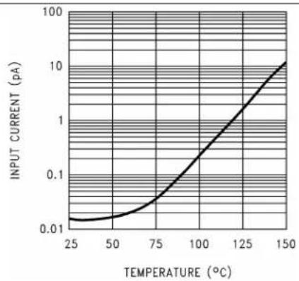
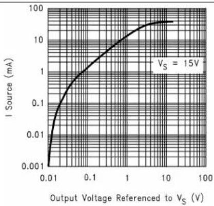
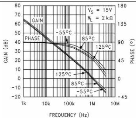
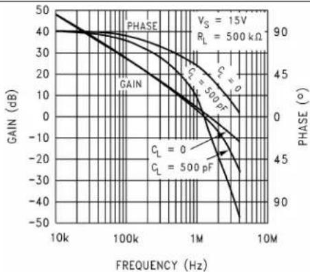
6.15TypicalCharacteristics
at V_S=15V , singlesupply, and T _A=25^ (unless otherwise specified)

line
| SUPPLY VOLTAGE (V) | +125°C | +85°C | +25°C | -55°C | | ------------------ | ------ | ----- | ----- | ----- | | 0 | 0.0 | 0.0 | 0.0 | 0.0 | | 2 | 0.5 | 0.7 | 0.9 | 0.6 | | 4 | 2.0 | 2.3 | 2.5 | 1.5 | | 6 | 2.5 | 2.7 | 2.8 | 1.7 | | 8 | 2.7 | 2.9 | 3.0 | 1.8 | | 10 | 2.8 | 3.0 | 3.1 | 1.9 | | 12 | 2.9 | 3.1 | 3.2 | 2.0 | | 14 | 3.0 | 3.2 | 3.3 | 2.1 | | 16 | 3.1 | 3.3 | 3.4 | 2.2 |Figure1. SupplyCurrentvsSupplyVoltage
line
| TEMPERATURE (°C) | INPUT CURRENT (pA) | | ---------------- | ------------------ | | 25 | 0.01 | | 50 | 0.01 | | 75 | 0.05 | | 100 | 0.5 | | 125 | 2.0 | | 150 | 10.0 |Figure2.InputCurrentvsTemperature
line
| Output Voltage Referenced to V_S (V) | I Source (mA) | | ------------------------------------- | ------------- | | 0.01 | 0.001 | | 0.1 | 0.1 | | 1 | 1 | | 10 | 10 | | 100 | 100 |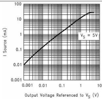
line
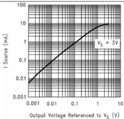
| Output Voltage Referenced to V_S (V) | I Source (mA) | | ------------------------------------- | ------------- | | 0.001 | 0.01 | | 0.01 | 0.1 | | 0.1 | 1 | | 1 | 10 | | 10 | 50 |Figure3.SourcingCurrentvsOutputVoltageFigure4.SourcingCurrentvsOutputVoltage
line
| Output Voltage Referenced to V_S (V) | I Source (mA) | | ------------------------------------- | ------------- | | 0.001 | 0.01 | | 0.01 | 0.1 | | 0.1 | 1 | | 1 | 10 | | 10 | 10 |Figure5.SourcingCurrentvsOutputVoltage

line
| Output Voltage Referenced to GND (V) | I Sink (mA) | | ------------------------------------- | ----------- | | 0.01 | 0.01 | | 0.1 | 1 | | 1 | 10 | | 10 | 100 | | 100 | 100 |Figure6.SinkingCurrentvsOutputVoltage
TypicalCharacteristics(continued)
at V_S = 15V , singlesupply, and T _A = 25^ (unless otherwise specified)

line
| Output Voltage Referenced to GND (V) | I Sink (mA) | | ------------------------------------- | ----------- | | 0.01 | 0.001 | | 0.1 | 0.1 | | 1 | 1 | | 10 | 10 |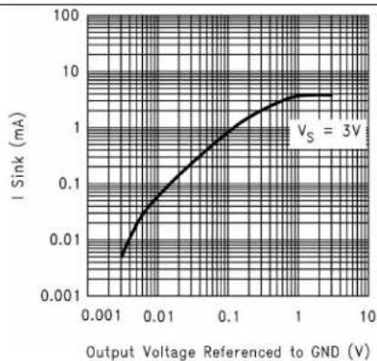
line
| Output Voltage Referenced to GND (V) | I Sink (mA) | | ------------------------------------- | ----------- | | 0.001 | 0.001 | | 0.01 | 0.01 | | 0.1 | 0.1 | | 1 | 1 | | 10 | 10 |Figure7.SinkingCurrentvsOutputVoltageFigure8.SinkingCurrentvsOutputVoltage

line
| SUPPLY VOLTAGE (V) | OUTPUT SWING FROM SUPPLY VOLTAGE (mV) | | ------------------ | -------------------------------------- | | 3 | 5 | | 6 | 5 | | 9 | 15 | | 12 | 21 | | 15 | 27 |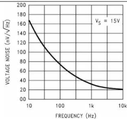
line
| FREQUENCY (Hz) | VOLTAGE NOISE (nV/√Hz) | | -------------- | ---------------------- | | 10 | 160 | | 100 | 80 | | 1k | 40 | | 10k | 20 |Figure9.OutputVoltageSwingvsSupplyVoltage
line
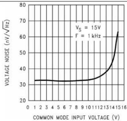
| COMMON MODE INPUT VOLTAGE (V) | VOLTAGE NOISE (nV/√Hz) | | ---------------------------- | ---------------------- | | 0 | 32 | | 1 | 32 | | 2 | 32 | | 3 | 32 | | 4 | 32 | | 5 | 32 | | 6 | 32 | | 7 | 32 | | 8 | 32 | | 9 | 32 | | 10 | 32 | | 11 | 32 | | 12 | 35 | | 13 | 40 | | 14 | 50 | | 15 | 60 | | 16 | 65 |Figure10.InputVoltageNoisevsFrequency

line
| COMMON MODE INPUT VOLTAGE (V) | VOLTAGE NOISE (nV/√Hz) | | ---------------------------- | ------------------------ | | 0 | 33 | | 1 | 34 | | 2 | 36 | | 3 | 40 | | 4 | 52 | | 5 | 54 |Figure11.InputVoltageNoisevsInputVoltageFigure12.InputVoltageNoisevsInputVoltage
TypicalCharacteristics(continued)
at V_S = 15V , singlesupply, and T _A = 25^ (unless otherwise specified)
line
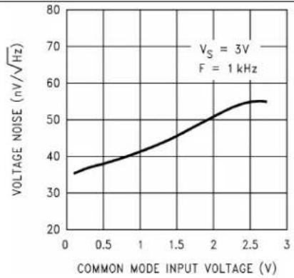
| COMMON MODE INPUT VOLTAGE (V) | VOLTAGE NOISE (nV/√Hz) | | ---------------------------- | ------------------------ | | 0.0 | 35.0 | | 0.5 | 38.0 | | 1.0 | 42.0 | | 1.5 | 46.0 | | 2.0 | 50.0 | | 2.5 | 55.0 | | 3.0 | 56.0 |Figure13.InputVoltageNoisevsInputVoltage
line
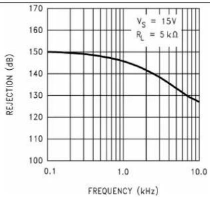
| FREQUENCY (kHz) | REJECTION (dB) | | --------------- | -------------- | | 0.1 | 150 | | 1.0 | 145 | | 10.0 | 128 |Figure14.CrosstalkRejectionvsFrequency
line
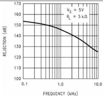
| FREQUENCY (kHz) | REJECTION (dB) | | --------------- | --------------- | | 0.1 | 155 | | 1.0 | 145 | | 10.0 | 125 |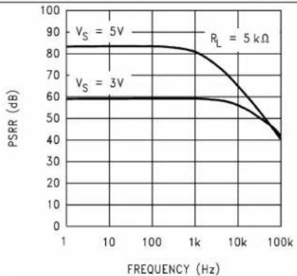
line
| FREQUENCY (Hz) | PSRR (dB) for V_S = 3V | PSRR (dB) for V_S = 5V | | -------------- | ---------------------- | ---------------------- | | 1 | 60 | 85 | | 10 | 60 | 85 | | 100 | 60 | 85 | | 1k | 60 | 80 | | 10k | 55 | 70 | | 100k | 45 | 40 |Figure15.CrosstalkRejectionvsFrequencyFigure16.PositivePSRRvsFrequency

line
| FREQUENCY (Hz) | PSRR (dB) for V_S = 3V | PSRR (dB) for V_S = 5V | | -------------- | ---------------------- | ---------------------- | | 1 | 80 | 82 | | 10 | 80 | 82 | | 100 | 80 | 82 | | 1k | 60 | 60 | | 10k | 40 | 40 | | 100k | 25 | 25 |
line
| FREQUENCY (Hz) | CMRR (dB) | | -------------- | --------- | | 10 | 95 | | 100 | 94 | | 1k | 92 | | 10k | 85 | | 100k | 75 |Figure17.NegativePSRRvsFrequencyFigure18.CMRRvsFrequency
TypicalCharacteristics(continued)
at V_S = 15V , singlesupply, and T _A = 25^ (unless otherwise specified)
line
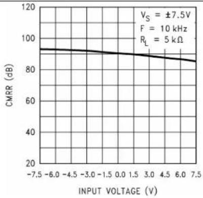
| INPUT VOLTAGE (V) | CMRR (dB) | | ----------------- | --------- | | -7.5 | 95 | | -6.0 | 94 | | -4.5 | 93 | | -3.0 | 92 | | -1.5 | 91 | | 0.0 | 90 | | 1.5 | 89 | | 3.0 | 88 | | 4.5 | 87 | | 6.0 | 86 | | 7.5 | 85 |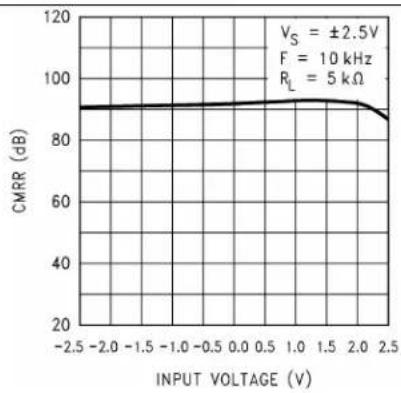
line
| INPUT VOLTAGE (V) | CMRR (dB) | | ----------------- | --------- | | -2.5 | 90 | | -2.0 | 90 | | -1.5 | 90 | | -1.0 | 90 | | -0.5 | 90 | | 0.0 | 90 | | 0.5 | 90 | | 1.0 | 90 | | 1.5 | 90 | | 2.0 | 85 | | 2.5 | 80 |Figure19.CMRRvsInputVoltageFigure20.CMRRvsInputVoltage
line
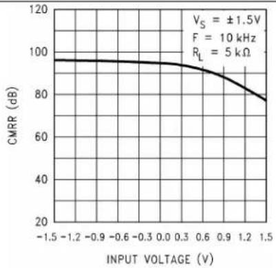
| INPUT VOLTAGE (V) | CMRR (dB) | | ----------------- | --------- | | -1.5 | 98 | | -1.2 | 97 | | -0.9 | 96 | | -0.6 | 95 | | -0.3 | 94 | | 0.0 | 93 | | 0.3 | 92 | | 0.6 | 90 | | 0.9 | 85 | | 1.2 | 78 | | 1.5 | 75 |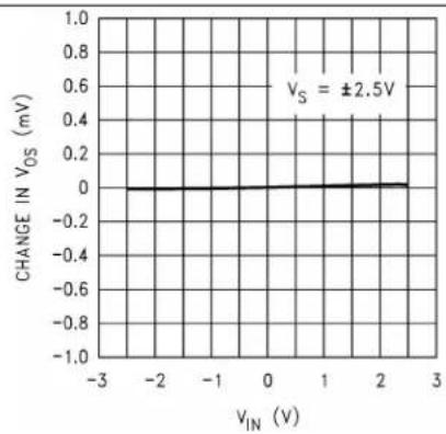
line
| VIN (V) | CHANGE IN VOS (mV) | | ------- | ------------------ | | -3 | 0 | | -2 | 0 | | -1 | 0 | | 0 | 0 | | 1 | 0 | | 2 | 0 | | 3 | 0 |Figure21.CMRRvsInputVoltage
line
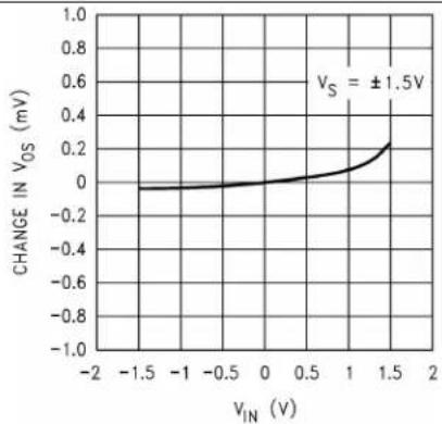
| VIN (V) | CHANGE IN VOS (mV) | | ------- | ------------------ | | -1.5 | 0.0 | | 0.0 | 0.0 | | 1.5 | 0.2 |Figure22.ΔV os vsCMR
line
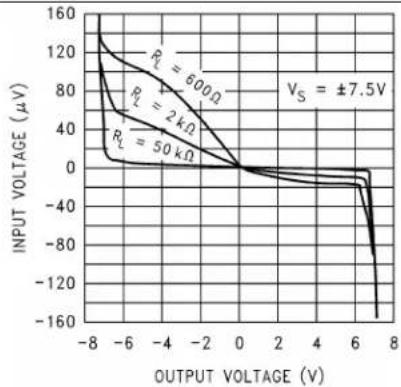
| OUTPUT VOLTAGE (V) | INPUT VOLTAGE (μV) for R_L = 50 kΩ | INPUT VOLTAGE (μV) for R_L = 2 kΩ | INPUT VOLTAGE (μV) for R_L = 600 Ω | | ------------------ | ---------------------------------- | ---------------------------------- | ---------------------------------- | | -8 | ~140 | ~140 | ~140 | | -6 | ~100 | ~100 | ~100 | | -4 | ~60 | ~60 | ~60 | | -2 | ~30 | ~30 | ~30 | | 0 | ~0 | ~0 | ~0 | | 2 | ~-30 | ~-30 | ~-30 | | 4 | ~-60 | ~-60 | ~-60 | | 6 | ~-90 | ~-90 | ~-90 | | 8 | ~-160 | ~-160 | ~-160 |Figure23.ΔV os vsCMR
Figure24.InputVoltagevsOutputVoltage
TypicalCharacteristics(continued)
at V_S = 15V , singlesupply, and T _A = 25^ (unless otherwise specified)

line
| OUTPUT VOLTAGE (V) | INPUT VOLTAGE (μV) for R_L = 50 kΩ | INPUT VOLTAGE (μV) for R_L = 2 kΩ | INPUT VOLTAGE (μV) for R_L = 600 Ω | | ------------------ | ---------------------------------- | ---------------------------------- | ---------------------------------- | | -3 | ~120 | ~100 | ~140 | | -2 | ~80 | ~60 | ~100 | | -1 | ~20 | ~10 | ~40 | | 0 | ~0 | ~0 | ~0 | | 1 | ~-20 | ~-20 | ~-20 | | 2 | ~-40 | ~-40 | ~-40 | | 3 | ~-160 | ~-160 | ~-160 |Figure25.InputVoltagevsOutputVoltage
line
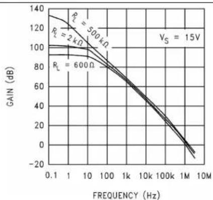
| FREQUENCY (Hz) | R_L = 2 kΩ | R_L = 500 kΩ | R_L = 600 Ω | | -------------- | ---------- | ------------ | ----------- | | 0.1 | ~135 | ~138 | ~140 | | 1 | ~125 | ~130 | ~135 | | 10 | ~110 | ~115 | ~120 | | 100 | ~95 | ~100 | ~105 | | 1k | ~80 | ~85 | ~90 | | 10k | ~60 | ~70 | ~75 | | 100k | ~30 | ~40 | ~45 | | 1M | ~0 | ~10 | ~15 | | 10M | ~-20 | ~-10 | ~-5 |Figure26.OpenLoopFrequencyResponse
line
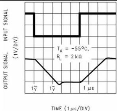
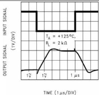
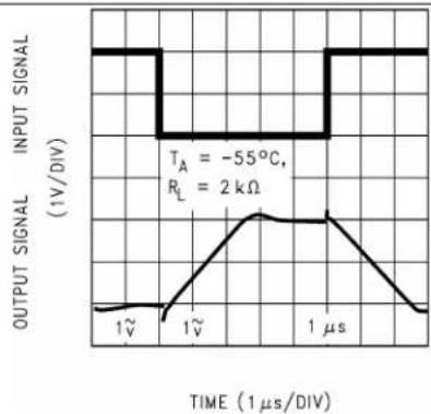
| TIME (1 µs/DIV) | INPUT SIGNAL (1V/DIV) | OUTPUT SIGNAL (1V/DIV) | | --------------- | --------------------- | ----------------------- | | 0 | 1 | 1 | | ~0.5 | 1 | ~0.5 | | ~1.0 | 1 | ~0.2 | | ~1.5 | 1 | ~0.3 | | ~2.0 | 1 | ~0.4 | | ~2.5 | 1 | ~0.6 | | ~3.0 | 1 | ~0.8 | | ~3.5 | 1 | ~0.9 | | ~4.0 | 1 | ~0.8 | | ~4.5 | 1 | ~0.7 | | ~5.0 | 1 | ~0.6 | | ~5.5 | 1 | ~0.5 | | ~6.0 | 1 | ~0.4 | | ~6.5 | 1 | ~0.3 | | ~7.0 | 1 | ~0.2 | | ~7.5 | 1 | ~0.1 | | ~8.0 | 1 | ~0.0 | | ~8.5 | 1 | ~0.1 | | ~9.0 | 1 | ~0.2 | | ~9.5 | 1 | ~0.3 | | ~10.0 | 1 | ~0.4 | | ~10.5 | 1 | ~0.5 | | ~11.0 | 1 | ~0.6 | | ~11.5 | 1 | ~0.7 | | ~12.0 | 1 | ~0.8 | | ~12.5 | 1 | ~0.9 | | ~13.0 | 1 | ~0.8 | | ~13.5 | 1 | ~0.7 | | ~14.0 | 1 | ~0.6 | | ~14.5 | 1 | ~0.5 | | ~15.0 | 1 | ~0.4 | | ~15.5 | 1 | ~0.3 | | ~16.0 | 1 | ~0.2 | | ~16.5 | 1 | ~0.1 | | ~17.0 | 1 | ~0.0 | | ~17.5 | 1 | ~0.1 | | ~18.0 | 1 | ~0.2 | | ~18.5 | 1 | ~0.3 | | ~19.0 | 1 | ~0.4 | | ~19.5 | 1 | ~0.5 | | ~20.0 | 1 | ~0.6 | | ~20.5 | 1 | ~0.7 | | ~21.0 | 1 | ~0.8 | | ~21.5 | 1 | ~0.9 | | ~22.0 | 1 | ~0.8 | | ~22.5 | 1 | ~0.7 | | ~23.0 | 1 | ~0.6 | | ~23.5 | 1 | ~0.5 | | ~24.0 | 1 | ~0.4 | | ~24.5 | 1 | ~0.3 | | ~25.0 | 1 | ~0.2 | | ~25.5 | 1 | ~0.1 | | ~26.0 | 1 | ~0.0 | | ~26.5 | 1 | ~0.1 | | ~27.0 | 1 | ~0.2 | | ~27.5 | 1 | ~0.3 | | ~28.0 | 1 | ~0.4 | | ~28.5 | 1 | ~0.5 | | ~29.0 | 1 | ~0.6 | | ~29.5 | 1 | ~0.7 | | ~30.0 | 1 | ~0.8 | | >30 | 1 | <0 | The chart displays two data series: one for input signal and one for output signal over time (in units of 1/μs/div). The input signal is labeled as 'T_A = +125°C' and the output signal is labeled as 'R_L = 2 kΩ'. The x-axis represents time in nanoseconds (from 0 to >30).
line
| TIME (1 μs/DIV) | INPUT SIGNAL (1V/DIV) | OUTPUT SIGNAL (1V/DIV) | | --------------- | --------------------- | ----------------------- | | 0 | 1 | 1 | | 1~v | 1 | 0.5 | | 1~u | 0.5 | 0.25 | | 1 μs | 1 | 0.75 |Figure27.NoninvertingLargeSignalPulseResponseFigure28.NoninvertingLargeSignalPulseResponse
line
| TIME (1 μs/DIV) | INPUT SIGNAL (1V/DIV) | OUTPUT SIGNAL (1V/DIV) | | --------------- | --------------------- | ----------------------- | | 0 | 1 | 1 | | 1 | 1 | 0.5 | | 2 | 1 | 0 | | 3 | 1 | 0.5 | | 4 | 1 | 1 | | 5 | 1 | 0.5 | | 6 | 1 | 1 | | 7 | 1 | 0.5 | | 8 | 1 | 0 | | 9 | 1 | 0.5 | | 10 | 1 | 1 | | 11 | 1 | 0.5 | | 12 | 1 | 0 | | 13 | 1 | 0.5 | | 14 | 1 | 1 | | 15 | 1 | 0.5 | | 16 | 1 | 0 | | 17 | 1 | 0.5 | | 18 | 1 | 1 | | 19 | 1 | 0.5 | | 20 | 1 | 0 | | 21 | 1 | 0.5 | | 22 | 1 | 1 | | 23 | 1 | 0.5 | | 24 | 1 | 0 | | 25 | 1 | 0.5 | | 26 | 1 | 1 | | 27 | 1 | 0.5 | | 28 | 1 | 0 | | 29 | 1 | 0.5 | | 30 | 1 | 1 | | | | |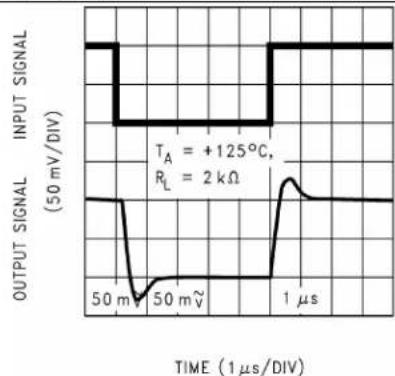
line
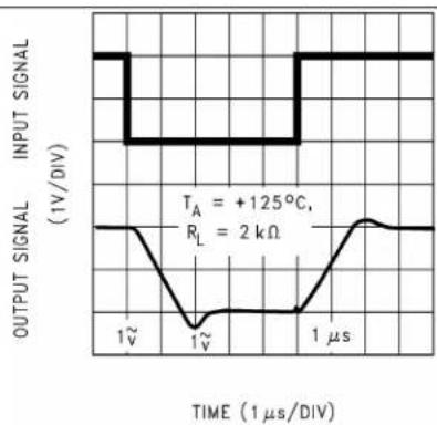
| TIME (1 µs/DIV) | INPUT SIGNAL (50 mV/DIV) | OUTPUT SIGNAL (50 mV/DIV) | | --------------- | ------------------------ | -------------------------- | | 0 | 125 | 50 | | 10 | 125 | 50 | | 20 | 125 | 50 | | 30 | 125 | 50 | | 40 | 125 | 50 | | 50 | 125 | 50 | | 60 | 125 | 50 | | 70 | 125 | 50 | | 80 | 125 | 50 | | 90 | 125 | 50 | | 100 | 125 | 50 | | 110 | 125 | 50 | | 120 | 125 | 50 | | 130 | 125 | 50 | | 140 | 125 | 50 | | 150 | 125 | 50 | | 160 | 125 | 50 | | 170 | 125 | 50 | | 180 | 125 | 50 | | 190 | 125 | 50 | | 200 | 125 | 50 | | 210 | 125 | 50 | | 220 | 125 | 50 | | 230 | 125 | 50 | | 240 | 125 | 50 | | 250 | 125 | 50 | | 260 | 125 | 50 | | 270 | 125 | 50 | | 280 | 125 | 50 | | 290 | 125 | 50 | | 300 | 125 | 50 | | 310 | 125 | 50 | | 320 | 125 | 50 | | 330 | 125 | 50 | | 340 | 125 | 50 | | 350 | 125 | 50 | | 360 | 125 | 50 | | 370 | 125 | 50 | | 380 | 125 | 50 | | 390 | 125 | 50 | | 400 | 125 | 50 | | 410 | 125 | 50 | | 420 | 125 | 50 | | 430 | 125 | 50 | | 440 | 125 | 50 | | 450 | 125 | 50 | | 460 | 125 | 50 | | 470 | 125 | 50 | | 480 | 125 | 50 | | 490 | 125 | 50 | | 50 | - | - | | Peak | - | - | | Final | - | - | | Current (T_A) | +125 | - | | Current (R_L) | +2 kΩ | - | | Time (μs) | - | - | | Time (μs) | - | - | | Time (μs) | - | - | | Time (μs) | - | - | | Time (μs) | - | - | | Time (μs) | - | - | | Time (μs) | - | - | | Time (μs) | - | ~+1.25 | | Time (μs) | - | ~+1.25 | | Time (μs) | - | ~+1.25 | | Time (μs) | - | ~+1.25 | | Time (μs) | - | ~+1.25 | | Time (μs) | - | ~+1.25 | | Time (µs) | - | ~+1.25 | | Time (µs) | - | ~+1.25 | | Time (µs) | - | ~+1.25 | | Time (µs) | - | ~+1.25 | | Time (µs) | - | ~+1.25 | | Time (µs) | ~+1.25 | ~+1.25 | | Time (µs) | ~+1.25 | ~+1.25 | | Time (µs) | ~+1.25 | ~+1.25 | | Time (µs) | ~+1.25 | ~+1.25 | | Time (µs) | ~+1.25 | ~+ | | Time (µs) | ~+1.25 | ~- | | Time (µs) | ~+1.25 | ~- | | Time (µs) | ~+1.25 | ~- | | Time (µs) | ~+1.25 | ~- | | Time (µs) | ~+ | ~- | | Time (µs) | ~- | ~- | | Time (µs) | ~- | ~- | | Time (µs) | ~- | ~- | | Time (µs) | ~- | ~- | | Time (µs) | ~- | ~- | | Time (µs) | ~- | ~- | | Time (µs) | ~- | ~ - | | Time (µs) | ~- | ~- | | Time (µs) | ~- | ~- | | Time (µs) | ~- | ~- | | Time (µs) | ~- | ~- | | Time (µs) | ~- | ~- | | Time (µs) | ~- | ~- | | T_A | +125 | - | | R_L | +2 kΩ | - | | Current (T_A)| - | - | | Current (R_L)| - | - | | Current (Time)| - | - | | Current (Time)| - | - | | Current (Time)| - | - | | Current (Time)| - | - | | Current (Time)| - | - | | Current (Time)| - | - | | Current (Time)| - | - | | Current (Time)| - | - | | Current (Time)| - | - | | Current (Time)| | Current (Time)| - | - | | Current (Time)| - | - | | Current (Time)| - | - | | Current (Time)| -Figure29.NoninvertingLargeSignalPulseResponseFigure30.NoninvertingSmallSignalPulseResponse
TypicalCharacteristics(continued)
at V_S = 15V , singlesupply, and T _A = 25^ (unless otherwise specified)

line
| TIME (1 µs/DIV) | OUTPUT SIGNAL (50 mV/DIV) | | --------------- | -------------------------- | | 0 | 50 | | 50 | -25 | | 100 | 25 | | 150 | -25 | | 200 | 25 | | 250 | -25 | | 300 | 25 | | 350 | -25 | | 400 | 25 | | 450 | -25 | | 500 | 25 | | 550 | -25 | | 600 | 25 | | 650 | -25 | | 700 | 25 | | 750 | -25 | | 800 | 25 | | 850 | -25 | | 900 | 25 | | 950 | -25 | | 1000 | 25 | | 1050 | -25 | | 1100 | 25 | | 1150 | -25 | | 1200 | 25 | | 1250 | -25 | | 1300 | 25 | | 1350 | -25 | | 1400 | 25 | | 1450 | -25 | | 1500 | 25 | | 1550 | -25 | | 1600 | 25 | | 1650 | -25 | | 1700 | 25 | | 1750 | -25 | | 1800 | 25 | | 1850 | -25 | | 1900 | 25 | | 1950 | -25 | | 2000 | 25 | | 2050 | -25 | | 2100 | 25 | | 2150 | -25 | | 2200 | 25 | | 2250 | -25 | | 2300 | 25 | | 2350 | -25 | | 2400 | 25 | | 2450 | -25 | | 2500 | 25 | | 2550 | -25 | | 2600 | 25 | | 2650 | -25 | | 2700 | 25 | | 2750 | -25 | | 2800 | 25 | | 2850 | -25 | | 2900 | 25 | | 2950 | -25 | | 3000 | 25 | | 3050 | -25 | | 3100 | 25 | | 3150 | -25 | | 3200 | 25 | | 3250 | -25 | | 3300 | 25 | | 3350 | -25 | | 3400 | 25 | | 3450 | -25 | | 3500 | 25 | | 3550 | -25 | | 3600 | 25 | | 3650 | -25 | | 3700 | 25 | | 3750 | -25 | | 3800 | 25 | | 3850 | -25 | | 3900 | 25 | | 3950 | -25 | | 4000 | 25 | | 4050 | -25 | | 4100 | 25 | | 4150 | -25 | | 4200 | 25 | | 4250 | -25 | | 4300 | 25 | | 4350 | -25 | | 4400 | 25 | | 4450 | -25 | | 4500 | 25 | | 4550 | -25 | | 4600 | 25 | | 4650 | -25 | | 4700 | 25 | | 4750 | -25 | | 4800 | 25 | | 4850 | -25 | | 4900 | 25 | | 4950 | -25 | | 500 | -3 |
line
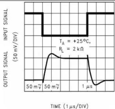
| TIME (1 µs/DIV) | OUTPUT SIGNAL (50 mV/DIV) | | --------------- | -------------------------- | | 0 | 50 | | ~0.5 | ~0 | | ~1.0 | ~0 | | ~1.5 | ~0 | | 1.0 | ~0 | | >1.0 | ~0 |Figure31.NoninvertingSmallSignalPulseResponseFigure32.NoninvertingSmallSignalPulseResponse
line
| TIME (1 μs/DIV) | OUTPUT SIGNAL (1V/DIV) | | --------------- | ------------------------ | | 0 | 0 | | 1 | 0 | | 2 | 0 | | 3 | 0 | | 4 | 0 | | 5 | 0 | | 6 | 0 | | 7 | 0 | | 8 | 0 | | 9 | 0 | | 10 | 0 | | 11 | 0 | | 12 | 0 | | 13 | 0 | | 14 | 0 | | 15 | 0 | | 16 | 0 | | 17 | 0 | | 18 | 0 | | 19 | 0 | | 20 | 0 | | 21 | 0 | | 22 | 0 | | 23 | 0 | | 24 | 0 | | 25 | 0 | | 26 | 0 | | 27 | 0 | | 28 | 0 | | 29 | 0 | | 30 | 0 | | 31 | 0 | | 32 | 0 | | 33 | 0 | | 34 | 0 | | 35 | 0 | | 36 | 0 | | 37 | 0 | | 38 | 0 | | 39 | 0 | | 40 | 0 | | 41 | 0 | | 42 | 0 | | 43 | 0 | | 44 | 0 | | 45 | 0 | | 46 | 0 | | 47 | 0 | | 48 | 0 | | 49 | 0 | | 50 | 0 | | 51 | 0 | | 52 | 0 | | 53 | 0 | | 54 | 0 | | 55 | 0 | | 56 | 0 | | 57 | 0 | | 58 | 0 | | 59 | 0 | | 60 | 0 | | 61 | 0 | | 62 | 0 | | 63 | 0 | | 64 | 0 | | 65 | 0 | | 66 | 0 | | 67 | 0 | | 68 | 0 | | 69 | 0 | | 70 | 0 | | 71 | 0 | | 72 | 0 | | 73 | 0 | | 74 | 0 | | 75 | 0 | | 76 | 0 | | 77 | 0 | | 78 | 0 | | 79 | 0 | | 80 | 0 | | 81 | 0 | | 82 | 0 | | 83 | 0 | | 84 | 0 | | 85 | 0 | | 86 | 0 | | 87 | 0 | | 88 | 0 | | 89 | 0 | | 90 | 0 | | 91 | 0 | | 92 | 0 | | 93 | 0 | | 94 | 0 | | 95 | 0 | | 96 | 0 | | 97 | 0 | | 98 | 0 | | 99 | 0 | | Note: The output signal values are not provided in the code. The input signal values are estimated based on the formula T_A = +125°C and R_L = -2 kΩ. There is no label for the data series. The output signal is calculated as the sum of the values from the input signal. There is only one data series in this case.
line
| TIME (1 µs/DIV) | INPUT SIGNAL (1V/DIV) | OUTPUT SIGNAL (1V/DIV) | | --------------- | --------------------- | ----------------------- | | 0 | 0 | 0 | | 1 | +25 | 0 | | 2 | +25 | Peak | | 3 | +25 | Peak | | 4 | +25 | Peak | | 5 | +25 | 0 | | 6 | +25 | 0 | | 7 | +25 | 0 | | 8 | +25 | 0 | | 9 | +25 | 0 | | 10 | +25 | 0 | | 11 | +25 | 0 | | 12 | +25 | 0 | | 13 | +25 | 0 | | 14 | +25 | 0 | | 15 | +25 | 0 | | 16 | +25 | 0 | | 17 | +25 | 0 | | 18 | +25 | 0 | | 19 | +25 | 0 | | 20 | +25 | 0 | | 21 | +25 | 0 | | 22 | +25 | 0 | | 23 | +25 | 0 | | 24 | +25 | 0 | | 25 | +25 | 0 | | 26 | +25 | 0 | | 27 | +25 | 0 | | 28 | +25 | 0 | | 29 | +25 | 0 | | 30 | +25 | 0 | | 31 | +25 | 0 | | 32 | +25 | 0 | | 33 | +25 | 0 | | 34 | +25 | 0 | | 35 | +25 | 0 | | 36 | +25 | 0 | | 37 | +25 | 0 | | 38 | +25 | 0 | | 39 | +25 | 0 | | 40 | +25 | 0 | | 41 | +25 | 0 | | 42 | +25 | 0 | | 43 | +25 | 0 | | 44 | +25 | 0 | | 45 | +25 | 0 | | 46 | +25 | 0 | | 47 | +25 | 0 | | 48 | +25 | 0 | | 49 | +25 | 0 | | 50 | +25 | 0 | | 51 | +25 | 0 | | 52 | +25 | 0 | | 53 | +25 | 0 | | 54 | +25 | 0 | | 55 | +25 | 0 | | 56 | +25 | 0 | | 57 | +25 | 0 | | 58 | +25 | 0 | | 59 | +25 | 0 | | 60 | +25 | 0 | | 61 | +25 | 0 | | 62 | +25 | 0 | | 63 | +25 | 0 | | 64 | +25 | 0 | | 65 | +25 | 0 | | 66 | +25 | 0 | | 67 | +25 | 0 | | 68 | +25 | 0 | | 69 | +25 | 0 | | 70 | +25 | 0 | | 71 | +25 | 0 | | 72 | +25 | 0 | | 73 | +25 | 0 | | 74 | +25 | 0 | | 75 | +25 | 0 | | 76 | +25 | 0 | | 77 | +25 | 0 | | 78 | +25 | 0 | | 79 | +25 | 0 | | 80 | +25 | 0 | | 81 | +25 | 0 | | 82 | +25 | 0 | | 83 | +25 | 0 | | 84 | +25 | 0 | | 85 | +25 | 0 | | 86 | +25 | 0 | | 87 | +25 | 0 | | 88 | +25 | 0 | | 89 | +25 | 0 | | 90 | +25 | 0 | | 91 | +25 | 0 | | 92 | +25 | 0 | | 93 | +25 | 0 | | 94 | +25 | 0 | | 95 | +25 | 0 | | 96 | +25 | 0 | | 97 | +25 | 0 | | 98 | +25 | 0 | | 99 | +25 | 0 | | Note: The output signal values are not provided in the code. The input signal values are labeled as '1V' and 'DIV'. The output signal values are labeled as '1̅V' and '1̅V'. There is no label for the output signal in the chart.Figure33.InvertingLargeSignalPulseResponseFigure34.InvertingLargeSignalPulseResponse
line
| TIME (1 μs/DIV) | OUTPUT SIGNAL (1V/DIV) | | --------------- | ------------------------ | | 0 | 0 | | ~0.5 | 0 | | ~1.0 | 0 | | ~1.5 | 0 | | ~2.0 | 0 | | ~2.5 | 0 | | ~3.0 | 0 | | ~3.5 | 0 | | ~4.0 | 0 | | ~4.5 | 0 | | ~5.0 | 0 | | ~5.5 | 0 | | ~6.0 | 0 | | ~6.5 | 0 | | ~7.0 | 0 | | ~7.5 | 0 | | ~8.0 | 0 | | ~8.5 | 0 | | ~9.0 | 0 | | ~9.5 | 0 | | 1.0 | 0 | | >1.0 | 0 |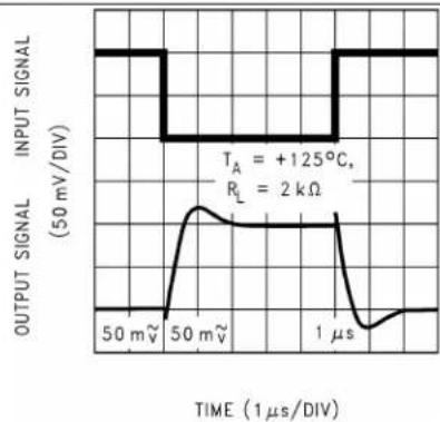
line
| TIME (1μs/DIV) | OUTPUT SIGNAL (50 mV/DIV) | | -------------- | -------------------------- | | 0 | 0 | | ~50 | ~0 | | ~100 | ~0 | | ~150 | ~0 | | ~200 | ~0 | | ~250 | ~0 | | ~300 | ~0 | | ~350 | ~0 | | ~400 | ~0 | | ~450 | ~0 | | ~500 | ~0 | | ~550 | ~0 | | ~600 | ~0 | | ~650 | ~0 | | ~700 | ~0 | | ~750 | ~0 | | ~800 | ~0 | | ~850 | ~0 | | ~900 | ~0 | | ~950 | ~0 | | 1μs | ~0 | | >1μs | ~0 |Figure35.InvertingLargeSignalPulseResponseFigure36.InvertingSmallSignalPulseResponse
TypicalCharacteristics(continued)
at V_S = 15V , singlesupply, and T _A = 25^ (unless otherwise specified)
line
| TIME (1 µs/DIV) | OUTPUT SIGNAL (50 mV/DIV) | | --------------- | -------------------------- | | 0 | 0 | | 50 | 0 | | 100 | 0 | | 150 | 0 | | 200 | 0 | | 250 | 0 | | 300 | 0 | | 350 | 0 | | 400 | 0 | | 450 | 0 | | 500 | 0 | | 550 | 0 | | 600 | 0 | | 650 | 0 | | 700 | 0 | | 750 | 0 | | 800 | 0 | | 850 | 0 | | 900 | 0 | | 950 | 0 | | 1000 | 0 | | 1050 | 0 | | 1100 | 0 | | 1150 | 0 | | 1200 | 0 | | 1250 | 0 | | 1300 | 0 | | 1350 | 0 | | 1400 | 0 | | 1450 | 0 | | 1500 | 0 | | 1550 | 0 | | 1600 | 0 | | 1650 | 0 | | 1700 | 0 | | 1750 | 0 | | 1800 | 0 | | 1850 | 0 | | 1900 | 0 | | 1950 | 0 | | 2000 | 0 | | 2050 | 0 | | 2100 | 0 | | 2150 | 0 | | 2200 | 0 | | 2250 | 0 | | 2300 | 0 | | 2350 | 0 | | 2400 | 0 | | 2450 | 0 | | 2500 | 0 | | 2550 | 0 | | 2600 | 0 | | 2650 | 0 | | 2700 | 0 | | 2750 | 0 | | 2800 | 0 | | 2850 | 0 | | 2900 | 0 | | 2950 | 0 | | 3000 | 0 | | 3050 | 0 | | 3100 | 0 | | 3150 | 0 | | 3200 | 0 | | 3250 | 0 | | 3300 | 0 | | 3350 | 0 | | 3400 | 0 | | 3450 | 0 | | 3500 | 0 | | 3550 | 0 | | 3600 | 0 | | 3650 | 0 | | 3700 | 0 | | 3750 | 0 | | 3800 | 0 | | 3850 | 0 | | 3900 | 0 | | 3950 | 0 | | 4000 | 0 | | Note: The output signal is scaled by -1 unit of voltage. The input signal is calculated as T_A = +25°C and R_L = -2 kΩ. There is no label for the output signal.
Figure37.InvertingSmallSignalPulseResponseFigure38.InvertingSmallSignalPulseResponse
line
| VOUT (V) | CAPACITIVE LOAD (pF) | | -------- | --------------------- | | -6 | ~100 | | -5 | ~100 | | -4 | ~100 | | -3 | ~100 | | -2 | ~100 | | -1 | ~100 | | 0 | ~100 | | 1 | ~100 | | 2 | ~100 | | 3 | ~100 | | 4 | ~100 | | 5 | ~100 | | 6 | ~100 |
line
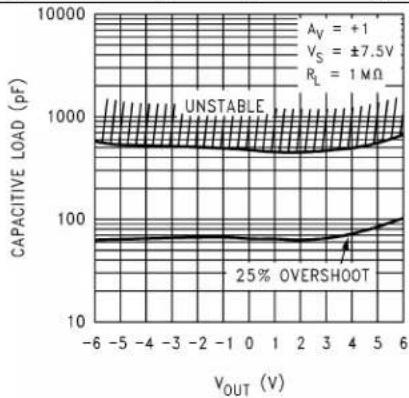
| VOUT (V) | CAPACITIVE LOAD (pF) | | -------- | --------------------- | | -6 | ~3000 | | -5 | ~2500 | | -4 | ~2000 | | -3 | ~1500 | | -2 | ~1000 | | -1 | ~800 | | 0 | ~50 | | 1 | ~70 | | 2 | ~100 | | 3 | ~150 | | 4 | ~200 | | 5 | ~250 | | 6 | ~300 |Figure39.StabilityvsCapacitiveLoadFigure40.StabilityvsCapacitiveLoad

line
| VOUT (V) | CAPACITIVE LOAD (pF) | | -------- | --------------------- | | -6 | ~10000 | | -5 | ~10000 | | -4 | ~10000 | | -3 | ~10000 | | -2 | ~10000 | | -1 | ~10000 | | 0 | ~100 | | 1 | ~10 | | 2 | ~10 | | 3 | ~10 | | 4 | ~10 | | 5 | ~10 | | 6 | ~10 |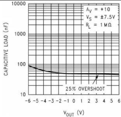
line
| VOUT (V) | CAPACITIVE LOAD (nF) | | -------- | --------------------- | | -6 | 100 | | -5 | ~80 | | -4 | ~60 | | -3 | ~50 | | -2 | ~40 | | -1 | ~35 | | 0 | ~30 | | 1 | ~28 | | 2 | ~25 | | 3 | ~22 | | 4 | ~20 | | 5 | ~18 | | 6 | ~15 |Figure41.StabilityvsCapacitiveLoadFigure42.StabilityvsCapacitiveLoad
TypicalCharacteristics(continued)
at V_S = 15V , singlesupply, and T _A = 25^ (unless otherwise specified)

line
| VOUT (V) | CAPACITIVE LOAD (nF) | | -------- | --------------------- | | -6 | 100 | | -5 | 100 | | -4 | 100 | | -3 | 100 | | -2 | 100 | | -1 | 100 | | 0 | 100 | | 1 | 100 | | 2 | 100 | | 3 | 100 | | 4 | 100 | | 5 | 100 | | 6 | 100 |
line
| VOUT (V) | CAPACITIVE LOAD (nF) | | -------- | --------------------- | | -6 | ~300 | | -5 | ~250 | | -4 | ~200 | | -3 | ~150 | | -2 | ~120 | | -1 | ~110 | | 0 | ~105 | | 1 | ~110 | | 2 | ~100 | | 3 | ~90 | | 4 | ~80 | | 5 | ~100 | | 6 | ~120 |Figure43.StabilityvsCapacitiveLoadFigure44.StabilityvsCapacitiveLoad
7DetailedDescription
7.1 Overview
TheLMC6484isaquadoperationalamplifierthatoffersalow-cost,low-poweramplifierforapplicationsrequiring multipleoperationalamplifierstagesandrail-to-railoperation. Thisdevicesupportsawidesupplyrange(3Vto 15V)andexcellentamplifier-to-amplifierisolation(150dBtypical). Thisdeviceisanexcellentchoiceforbattery-poweredsignalacquisitionsystemsrequiringhighlyintegratedsolutionstoachieveefficientlayout.
7.2 FunctionalBlockDiagram
text_image
14 13 12 11 10 9 8 4 V- 3 + 1 + - 2 V+ 5 6 7 1 2 3 4 5 6 77.3FeatureDescription
7.3.1 Amplifier Topology
TheLMC6484incorporatesspeciallydesigned,wide-complianceangecurrentmirrors,andthebodyeffectto extendinputcommon-moderangetoeachsupplyrail.Complementary,paralleled,differentialinputstages,like thetypeusedinotherCMOSandbipolarrail-to-railinputamplifiers,arenotusedbecauseoftheirinherent accuracyproblemsduetoCMRR,crossoverdistortion,andopen-loopgainvariation.
The input staged design of the LMC6484 is complemented by an output stage capable of rail-to-rail output swing even when driving a largeload. Rail-to-rail output swing is obtained by taking the output directly from the internal integrator instead of an output buffer stage.
7.3.2 InputCommon-ModeVoltageRange
UnlikeBi-FETamplifierdesigns,theLMC6484doesnotexhibitphaseinversionwhenaninputvoltageexceeds the negative supply voltage. Figure 46 shows an input voltage exceeding both supplies with no resulting phase inversionontheoutput.

line
| Time (μs) | Voltage (V) | | --------- | ----------- | | 500 | 0 | | 500 | 1.16 | | 500 | 3 |Figure45.AnInputVoltageSignalExceedstheLMC6484 PowerSupplyVoltagesWithNoOutputPhaseInversion
FeatureDescription(continued)
The absolutemaximuminputvoltageis300mVbeyondeithersupplyrailatroomtemperature.Voltagesgreatly exceeding this absolute maximum rating, as in Figure 46, can cause excessive current to flow in or out of the inputpinspossiblyaffectingreliability.
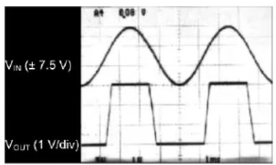
line
| Voltage Level | Description | | ------------- | ------------------- | | ±7.5 V | V_IN | | 1 V/div | V_OUT |Figure46.A±7.5VInputSignalGreatlyExceedsthe3-V SupplyinFigure47CausingNoPhaseInversionduetoR
Applicationsthatexceedthisratingmustexternallylimitthemaximuminputcurrentto±5mAwithaninput resistor,asshowninFigure47.
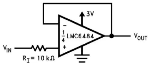
text_image
3V - ½ LMC6484 + VIN R1= 10 kΩ VOUTFigure47.R , InputCurrentProtectionforVoltagesExceedingtheSupplyVoltage
7.3.3 Rail-to-RailOutput
The approximated output resistance of the LMC6484 is 180- sourcing and 130- sinking at V_S=3V , and 110- sourcing and 83- sinking at V_S=5V . Using the calculated output resistance, the maximum output voltage swing can be estimated as a function of load.
7.4DeviceFunctionalModes
The LMC6482 may be used in applications where each amplifier channel is used independently, or in applications with cascaded channels. See the Typical Application section for more information.
8ApplicationandImplementation
NOTE
InformationinthefollowingapplicationssectionsisnotpartoftheTlcomponent specification,andTldoesnotwarrantitsaccuracyorcompleteness.TI'scustomersare responsiblefordeterminingsuitabilityofcomponentsfortheirpurposes.Customersshould validateandtesttheirdesignimplementationtoconfirmsystemfunctionality.
8.1 Application Information
8.1.1 Upgrading Applications
TheLMC6484quad-channeldevicesandLMC6482dual-channeldeviceshaveindustrystandardpinoutstorefitexistingapplications.SystemperformancecanbegreatlyincreasedbythefeaturesoftheLMC6484.ThekeybenefitofdesigningintheLMC6484isincreasedlinearsignalrange.Mostoperationalamplifiershavelimitedinputcommon-moderanges.Signalsthatexceedthisrangegenerateanonlinearoutputresponsethatpersistslongaftertheinputsignalreturnstothecommon-moderange.
Linearsignalrangeisvitalinapplicationssuchasfilters,wheresignalpeakingcanexceedinputcommon-mode ranges,andresultinoutputphaseinversionorseveredistortion.
8.1.2 Spice Macromodel
AspicemacromodelisavailablefortheLMC6484. Thismodelincludesaccuratesimulationofthefollowing:
• Inputcommon-modevoltagerange
• Frequency and transient response
• GBWdependenceonloadingconditions
• Quiescentanddynamicsupplycurrent
• Outputswingdependenceonloadingconditions
• Manymorecharacteristics,aslistedonthemacromodeldisk.
ContactyourlocalTexasInstrumentssalesofficetoobtainanoperationalamplifierspicemodellibrarydisk.
8.2 Typical Application

text_image
RF CF - + VIN RO VOUT CLFigure48. UnityGainBufferforHigh-CapacitiveLoads
TypicalApplication(continued)
8.2.1 DesignRequirements
- Forbestperformance, makesurethattheinputvoltageswingisbetweenV+andV-.
- Makesurethattheinputdoesnotexceedthecommon-modeinputrange.
- Toreducetheriskofde-stabilizingtheoutput,useresistiveisolationontheoutputwhendrivingcapacitive loads(seetheCapacitiveLoadCompensationsection).
- When large feedback resistors are used, compensate for parasitic capacitance on the input as needed (see the Compensating for Input Capacitances section).
8.2.2 Detailed Design Procedure
8.2.2.1 Capacitive Load Compensation
TheLMC6484typicallydirectlydrivesa100-pFloatwithV _S =15Vatunitygainwithoutoscillating.Theunity gainfolloweristhemostsensitiveconfiguration.Directcapacitiveloadingreducesthephasemarginof operationalamplifiers.Thecombinationoftheoutputimpedanceoftheoperationalamplifierandthecapacitive loadinducesphaselagthatresultsineitheranunder-dampedpulseresponseoroscillation.
Capacitive load compensation can be accomplished using resistive isolation, as shown in Figure 49. This simple technique is useful for isolating the capacitive input of multiplexers and analog-to-digital converters (ADCs).

text_image
- 1/4 LMC6484 + R = 300 Ω C_L = 330 pFFigure49.Resistivelsolationofa330-pFCapacitiveLoad
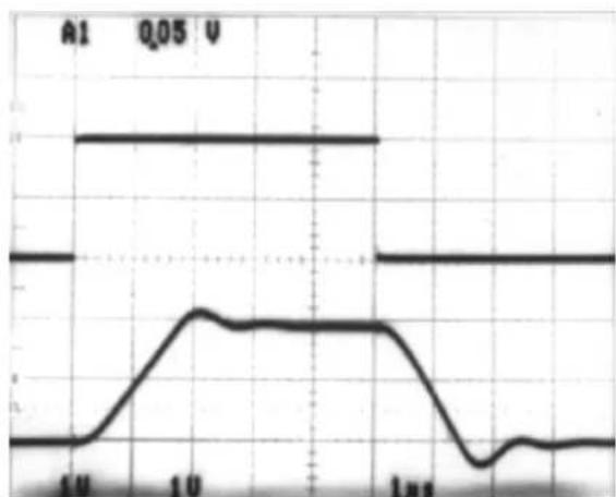
line
| Time | Value | |------|-------| | 10 | Low | | 10 | Peak | | 10 | High | | 1ns | Low |Figure50.PulseResponseoftheLMC6484CircuitinFigure49
TypicalApplication(continued)
Improved frequency response is achieved by indirectly driving capacitive loads as shown in Figure 51.

text_image
10 kΩ C₁ 100 pF - ½ LMC6484 + Vₐₙ R1 300Ω Vₒᵤₜ Cₗ = 330 pFFigure51.LMC6484NoninvertingAmplifierCompensatedtoHandlea330-pFCapacitiveLoad
R1 and C1 servetocounteractthelossofphasemarginbyfeedingforwardthehigh-frequencycomponentofthe outputsignalbacktotheinvertinginputoftheamplifier;thereby,preservingphasemarginintheoverallfeedback loop. ThevaluesofR1 and C1 areexperimentallydeterminedforthedesiredpulseresponse. Theresultingpulse responseisseeninFigure52.

line
| Time (μs) | Voltage (V) | | --------- | ----------- | | 0 | 0 | | 1 | ~500 | | 2 | ~450 | | 3 | ~400 | | 4 | ~350 | | 5 | ~300 | | 6 | ~250 | | 7 | ~200 | | 8 | ~150 | | 9 | ~100 | | 10 | ~50 | | 11 | ~25 | | 12 | ~10 | | 13 | ~5 | | 14 | ~2 | | 15 | ~1 | | 16 | ~0.5 | | 17 | ~0.2 | | 18 | ~0.1 | | 19 | ~0.05 | | 20 | ~0.02 | | 21 | ~0.01 | | 22 | ~0.005 | | 23 | ~0.002 | | 24 | ~0.001 | | 25 | ~0.0005 | | 26 | ~0.0002 | | 27 | ~0.0001 | | 28 | ~0.00005 | | 29 | ~0.00002 | | 30 | ~0.00001 | | 31 | ~0.000005 | | 32 | ~0.000002 | | 33 | ~0.000001 | | 34 | ~0.0000005 | | 35 | ~0.0000002 | | 36 | ~0.0000001 | | 37 | ~0.00000005 | | 38 | ~0.00000002 | | 39 | ~0.00000001 | | 40 | ~0.000000005| | 41 | ~0.000000002| | 42 | ~0.000000001| | 43 | ~0.0000000005| | 44 | ~0.0000000002| | 45 | ~0.0000000001| | 46 | ~0.00000000005| | 47 | ~5 | | 48 | ~2 | | 49 | ~1 | | 50 | ~0.5 | | 51 | ~-1 | | 52 | -2 | | 53 | -3 | | 54 | -4 | | 55 | -5 | | 56 | -6 | | 57 | -7 | | 58 | -8 | | 59 | -9 | | 60 | -10 | | 61 | -11 | | 62 | -12 | | 63 | -13 | | 64 | -14 | | 65 | -15 | | 66 | -16 | | 67 | -17 | | 68 | -18 | | 69 | -19 | | 70 | -20 | | 71 | -21 | | 72 | -22 | | 73 | -23 | | 74 | -24 | | 75 | -25 | | 76 | -26 | | 77 | -27 | | 78 | -28 | | 79 | -29 | | 80 | -30 | | 81 | -31 | | 82 | -32 | | 83 | -33 | | 84 | -34 | | 85 | -35 | | 86 | -36 | | 87 | -37 | | 88 | -38 | | 89 | -39 | | 90 | -40 | | 91 | -41 | | 92 | -42 | | 93 | -43 | | 94 | -44 | | 95 | -45 | | 96 | -46 | | 97 | -47 | | 98 | -48 | | 99 | -49 | | 100 | -5 |Figure52.PulseResponseofLMC6484CircuitinFigure51
Typical Application (continued)
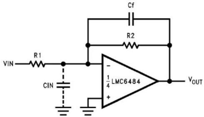
8.2.2.2 Compensating for Input Capacitance
Large values of feedback resistance are often used with amplifiers that have ultra-low input current, such as the LMC6484. Large feedback resistors can react with small values of input capacitance due to transducers, photodiodes, and circuit-board parasitics to reduce phase margins.
text_image
Vin R1 CIN Cf R2 - ½ LMC6484 + VOUTFigure 53. Canceling the Effect of Input Capacitance
To compensate for the effect of input capacitance, add a feedback capacitor. The feedback capacitor (as in Figure 53), Cf, is first estimated by Equation 1:
$$ \begin{array}{l} \frac {1}{2 \pi R C _ {1 N - 2} R ^ {\prime}} \geq \frac {1}{\pi} \ \text {or} \ R _ {1} C _ {1 N - 2} R ^ {\prime} G \end{array} \tag {1} $$
This equation typically provides significant overcompensation. Printed circuit board (PCB) stray capacitance may be larger or smaller than that of a breadboard, so the actual optimum value for C_f may be different. The values of Cf should be checked on the actual circuit. See the LMC660 Quad CMOS Amplifier data sheet for a more detailed discussion.
8.2.2.3 Offset Voltage Adjustment
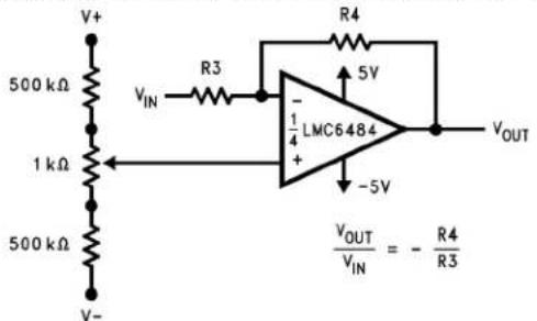
Offset voltage adjustment circuits are illustrated in Figure 54 and Figure 55. Large-value resistances and potentiometers are used to reduce power consumption while providing typically ±2.5 mV of adjustment range, referred to the input, for both configurations with V_S=±5 V.
text_image
V+ 500 kΩ 1 kΩ 500 kΩ V- R3 VIN R4 5V ½ LMC6484 + -5V VOUT VOUT/VIN = - R4/R3Figure 54. Inverting Configuration Offset Voltage Adjustment

text_image
V+ 500 kΩ R1 200 kΩ R3 R4 5V - ½ LMC6484 - VIN + -5V VOUT VIN = 1 + R4 / R3 ; R2 << R3Figure 55. Noninverting Configuration Offset Voltage Adjustment
TypicalApplication(continued)
8.2.3 ApplicationCurves

line
| FREQUENCY (Hz) | R_L = 500 kΩ | R_L = 2 kΩ | R_L = 600 Ω | | -------------- | ------------ | ---------- | ----------- | | 0.1 | ~100 | ~95 | ~60 | | 1 | ~98 | ~90 | ~55 | | 10 | ~95 | ~85 | ~50 | | 100 | ~90 | ~75 | ~45 | | 1k | ~80 | ~65 | ~40 | | 10k | ~60 | ~45 | ~25 | | 100k | ~30 | ~20 | ~10 | | 1M | ~0 | ~-5 | ~-15 | | 10M | ~-15 | ~-20 | ~-25 |Figure56.OpenLoopFrequencyResponse
line
| FREQUENCY (Hz) | GAIN (dB) | PHASE (°) | | -------------- | --------- | --------- | | 1k | 65 | 135 | | 10k | 40 | 90 | | 100k | 20 | 45 | | 1M | 0 | 0 | | 10M | -20 | -45 |Figure57.OpenLoopFrequencyResponsevs Temperature

line
| FREQUENCY (kHz) | OUTPUT SWING (V_PP) | | --------------- | ------------------- | | 0.1 | 14.5 | | 1 | 14.5 | | 10 | 14.5 | | 100 | 5.0 |Figure58.MaximumOutputSwingvsFrequency
line
| FREQUENCY (Hz) | GAIN (dB) | PHASE (°) | | -------------- | --------- | --------- | | 10k | 50 | 90 | | 100k | 30 | 85 | | 1M | 10 | 75 | | 10M | -50 | 60 |Figure59.GainandPhasevsCapacitiveLoad

line
| FREQUENCY (Hz) | GAIN (dB) | PHASE (°) | | -------------- | --------- | --------- | | 10k | 40 | 90 | | 100k | 20 | 45 | | 1M | 0 | 45 | | 10M | -50 | 90 |Figure60.GainandPhasevsCapacitiveLoadFigure61.OpenLoopOutputImpedancevsFrequency
line
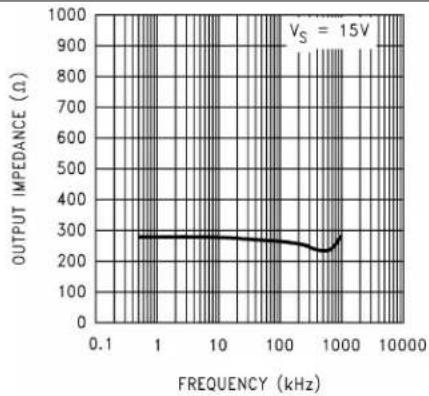
| FREQUENCY (kHz) | OUTPUT IMPEDANCE (Ω) | | --------------- | -------------------- | | 0.1 | 280 | | 1 | 280 | | 10 | 280 | | 100 | 260 | | 1000 | 240 | | 10000 | 280 |TypicalApplication(continued)

line
| FREQUENCY (kHz) | OUTPUT IMPEDANCE (Ω) | | --------------- | -------------------- | | 0.1 | 350 | | 1 | 350 | | 10 | 350 | | 100 | 300 | | 1000 | 280 | | 10000 | 350 |Figure62.OpenLoopOutputImpedancevsFrequency
line
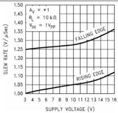
| SUPPLY VOLTAGE (V) | SLEW RATE (V/μSec) - RISING EDGE | SLEW RATE (V/μSec) - FALLING EDGE | | ------------------ | --------------------------------- | ---------------------------------- | | 3 | 1.00 | 1.25 | | 4 | 1.01 | 1.26 | | 5 | 1.02 | 1.27 | | 6 | 1.03 | 1.28 | | 7 | 1.04 | 1.29 | | 8 | 1.05 | 1.30 | | 9 | 1.06 | 1.31 | | 10 | 1.07 | 1.32 | | 11 | 1.08 | 1.33 | | 12 | 1.09 | 1.34 | | 13 | 1.10 | 1.35 | | 14 | 1.11 | 1.36 | | 15 | 1.12 | 1.37 | | 16 | 1.13 | 1.38 |Figure63.SlewRatevsSupplyVoltage
8.3SystemExamples
The circuit in Figure 64 uses a single supply to half-wave rectify a sinusoid centered about ground. R_1 limits current into the amplifier caused by the input voltage exceeding the supply voltage. Figure 65 shows the half-waverectifier waveform. Full-waverectification is provided by the circuit in Figure 66.

text_image
V+ = 3V 10 kΩ - ½ LMC6484 + VIN R1 VOUT 10 kΩFigure64. Half-WaveRectifierWithInputCurrentProtection(R)

line
| Time (ns) | Amplitude (A) | | --------- | ------------- | | 1 | 0 | | 10 | 0.9 | | 20 | 0 | | 200 | 0.9 | | 30 | 0 |Figure65.Half-WaveRectifierWaveform

text_image
V+ 10 kΩ R₁ - ½ LMC6484 + 10 kΩ 1N914Figure66.FullWaveRectifierWithInputCurrentProtection(R
SystemExamples(continued)
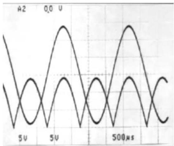
line
| Time (μs) | A2 (V) | 0.0 V | |-----------|--------|-------| | 5 | - | - | | 5 | + | - | | 50 | - | - | | 50 | + | - | | 500 | - | - | | 500 | + | - |Figure67.FullWaveRectifierWaveform

text_image
V+ R - ½ LMC6484 VIN IOUT = (V+ - VIN)/RFigure68. Large Compliance Range Current Source
text_image
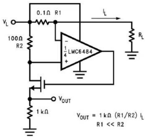
0.1Ω R1 100Ω R2 - 1/4 LMC6484 + VOUT 1 kΩ VOUT = 1 kΩ (R1/R2) IL R1 << R2 IL RLFigure69. PositiveSupplyCurrentSense
SystemExamples(continued)
In Figure 70, dielectric absorption and leakage is minimized by using a polystyrene or polyethylene hold capacitor. The droop rate is primarily determined by the value of CH and the diode leakage current. The ultra-low input current of the LMC6484 has a negligible effect on droop.
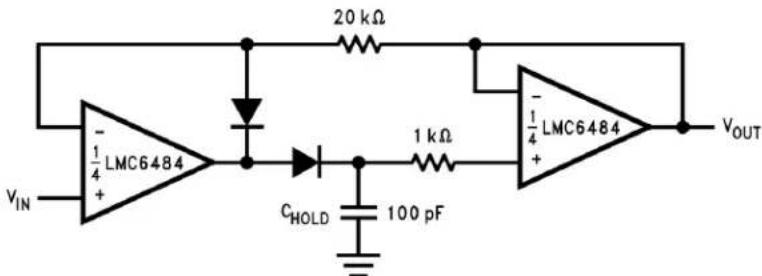
text_image
20 kΩ - 1/4 LMC6484 + - VIN C HOLD 100 pF 1 kΩ - 1/4 LMC6484 + VOUTFigure 70. Low Voltage Peak Detector With Rail-to-Rail Peak Capture Range
text_image
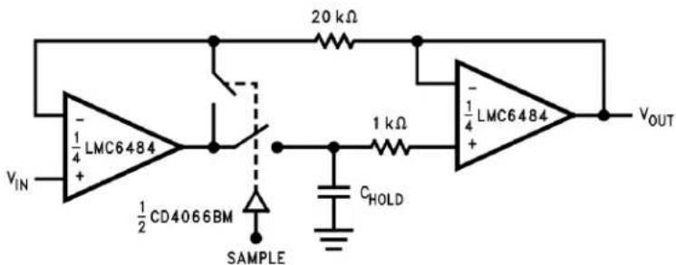
20 kΩ - 1/4 LMC6484 + 1 kΩ - 1/4 LMC6484 + VOUT VIN ½ CD4066BM SAMPLE CHOLDFigure 71. Rail-to-RailSample andHold
The high CMRR (85 dB) of the LMC6484 allows excellent accuracy throughout the rail-to-rail dynamic capture range of the circuit.
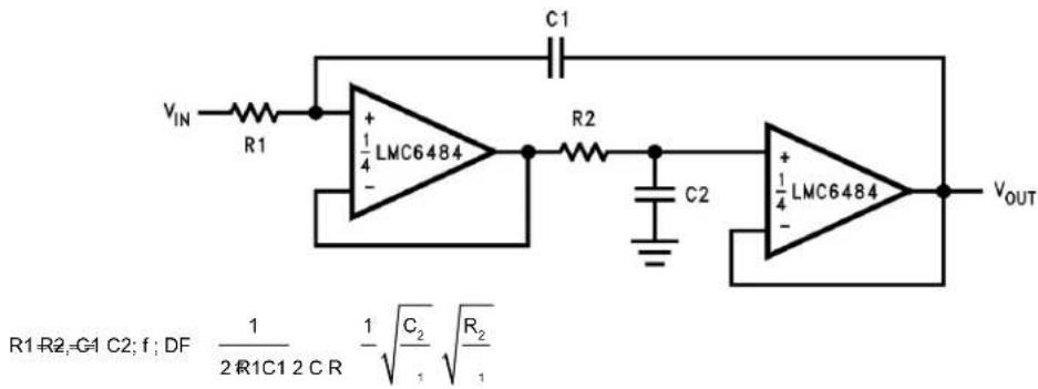
The low-pass filter circuit in Figure 72 can be used as an antialiasing filter with the same voltage supply as the ADC. Filter designs can also take advantage of the LMC6484 ultra-low input current. The ultra-low input current yields negligible offset error even when large value resistors are used, which allows the use of smaller-valued capacitors that take up less board space and cost less.
text_image
C1 VIN R1 + ¼ LMC6484 - R2 + ¼ LMC6484 - VOUT R1 R2 G1 C2; f ; DF 1/2 R1C1 2 CR 1√C2/3 √R2/3Figure 72. Rail-to-Rail, Single-Supply, Low-Pass Filter
SystemExamples(continued)
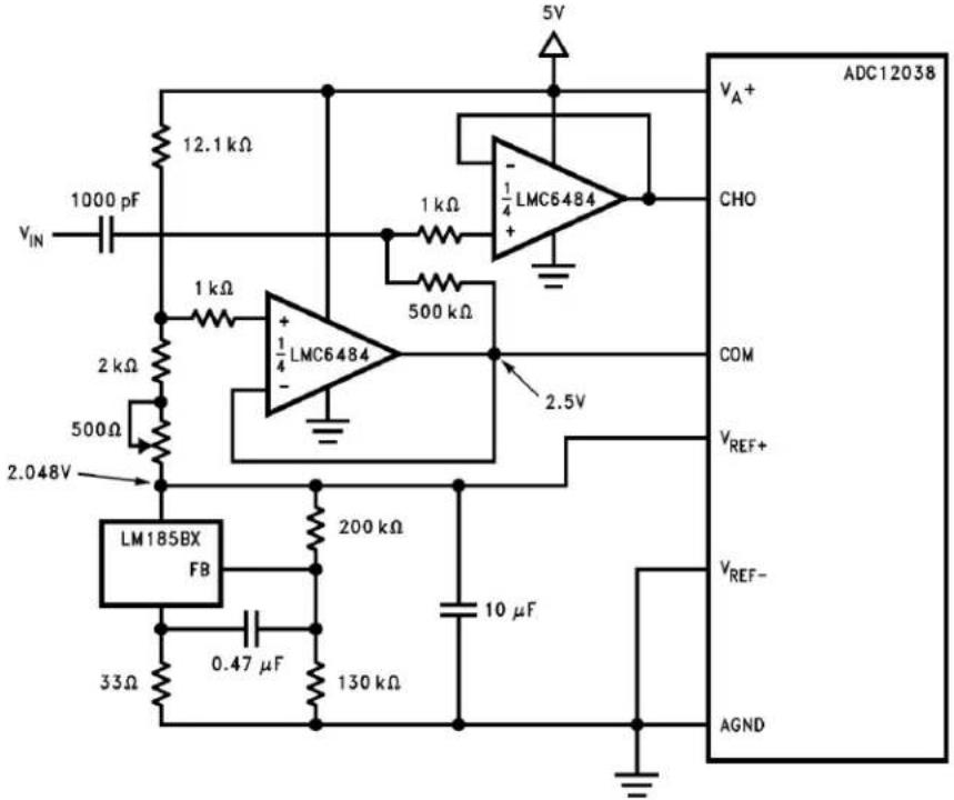
8.3.1 DataAcquisitionSystems
Low-power, single-supply, data acquisition system solutions are provided by buffering the ADC12038 with the LMC6484, as shown in Figure 73. Capable of using the full supply range, the LMC6484 does not require input signalstobescaleddowntomeetlimitedcommon-modevoltageranges.TheLMC6484CMRRof82dB maintainsintegrallinearityofa12-bitdataacquisitionsystemto±0.325LSB. Otherail-to-railinputamplifiers withonly50dBofCMRRdegradetheaccuracyofthedataacquisitionsystemtoonly8bits.
text_image
5V 12.1 kΩ 1 kΩ LMC6484 - ½ + VA+ ADC12038 CHO 1000 pF 1 kΩ 500 kΩ COM 2.5V 2 kΩ ½ LMC6484 2.048V 500Ω LM185BX FB 200 kΩ 33Ω 0.47 μF 130 kΩ 10 μF VREF+ VREF- AGNDFigure73. Operating From the Same Supply Voltage, the LMC6484 Buffer the ADC12038 Maintaining Excellent Accuracy
SystemExamples(continued)
8.3.2 Instrumentation Circuits
TheLMC6484hasthehighinputimpedance,largecommon-moderange,andhighCMRRrequiredfordesigning instrumentationcircuits.InstrumentationcircuitsdesignedwiththeLMC6484canrejectalargerrangeof common-modesignalsthanmostinstrumentationamps.Thus,instrumentationcircuitsdesignedwiththe LMC6484areanexcellentchoicefornoisyorindustrialenvironments.Otherapplicationsthatbenefitfromthese featuresincludeanalyticmedicalinstruments,magneticfielddetectors,gasdetectors,andsilicon-based transducers.
Asmall-valuedpotentiometerisusedinserieswithRgtosetthedifferentialgainofthethree-op-amp instrumentation circuit in Figure 74. This combination is used instead of one large valued potentiometer to increasegaintrimaccuracyandreduceerrorduetovibration.

text_image
10 kΩ R1 A1 ½ LMC6484 - 50 kΩ, 0.1% 0.1% 50 kΩ C2 RG C3 VIN R1 50 kΩ, 0.1% - A2 ½ LMC6484 + 50 kΩ 0.1% 50 kΩ C1 10 pF C4 3-20 pF AC CMR ADJUST 50 kΩ, 0.1% -A3 ½ LMC6484 + VOUT 48.7 kΩ DC CMR ADJUST R2 500Ω VREFERENCEFigure74.Low-Power,Three-Op-AmplInstrumentationAmplifier
A two-op-amp instrumentation amplifier designed for a gain of 100 is shown in Figure 75. Low sensitivity trimmingismadeforoffsetvoltage, CMRR, and gain. Low cost and low power consumption are the main advantages of this two-op-amp circuit.
Higher frequency and larger common-mode range applications are best facilitated by a three-op-amp instrumentationamplifier.

text_image
CMRR Trim 50Ω VCM + 1/2VD 9.95k 10k, 0.1% 191Ω 10Ω Gain Trim + A1 ½ LMC6484 - 10k, 0.1% 10k, 0.1% -VCM - 1/2VD - A2 ½ LMC6484 + VOUT = 100VDFigure75.Low-PowerTwo-Op-AmplInstrumentationAmplifier
9PowerSupplyRecommendations
TheLMC6482canbeoperatedoverasupplyrangeof3Vto15V.Toachievenoiseimmunityasappropriateto theapplication,makesuretousegoodPCBlayoutpracticesforpowersupplyrailsandplanes,aswellasusing bypasscapacitorsconnectedbetweenthepowersupplypinsandground.
10Layout
10.1 LayoutGuidelines
10.1.1 Printed-Circuit-BoardLayoutforHigh-ImpedanceWork
Anycircuitthatmustoperatewithlessthan1000pAofleakagecurrentrequiresspeciallayoutofthePCB. To takeadvantageoftheultra-lowinputcurrentoftheLMC6484(typically,lessthan20fA),makesuretohavean excellentlayout. Fortunately,thetechniquesforobtaininglowleakagesarequitesimple.First,donotignorethe surfaceleakageofthePCB,eventhoughthisleakagemaysometimesappearacceptablylow,becauseunder conditionsofhighhumidityordustorcontamination,thesurfaceleakagewillbeappreciable.
Tominimizetheeffectofanysurfaceleakage,layoutaringoffoilcompletelysurroundingtheLMC6484inputs andtheterminalsofcapacitors,diodes,conductors,resistors,relayterminals,ansoon,connectedtothe operational amplifier inputs, as in Figure 78. To have a significant effect, place guard rings in both the top and bottomofthePCB.ThisPCfoilmustthenbeconnectedtoavoltagethatisatthesamevoltageastheamplifier inputs,becauseonoleakagecurrentcanflowbetweenwopointsatthesamepotential.Forexample,aPCB trace-to-padresistanceof10 ^12 ,whichisnormallyconsideredaverylargeresistance,couldleak5pAifthe tracewerea5-Vbusadjacenttotherpadoftheinput.Thisleakagewouldcausea250timesdegradationfrom theactualperformanceoftheLMC6484.However,ifaguardringisheldwithin5mVoftheinputs,thenevena resistanceof10 ^11 would cause only 0.05 pA of leakage current. Figure 76 shows the typical connections of guardringsforstandardoperationalamplifierconfigurations.

text_image
INPUT - ½ LMC6484 + OUTPUTFigure76. TypicalConnectionsofGuardRings
BeawarethatwhenitisinappropriatetolayoutaPCBforthesakeofjustafewcircuits,anothertechniqueeven better than a guard ring on a PCB: do not insert the input pin of the amplifier into the PCB at all, but bend the inputpinupintheairanduseonlyairasaninsulator.Airisanexcellentinsulator.Inthiscase,youmayhaveto foregosomeoftheadadvantagesofPCBconstruction,buttheadvantagesaresometimeswellworththeeffortof usingpoint-to-point,up-in-the-airwiring,asshowninFigure77.
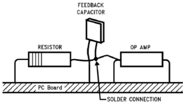
text_image
FEEDBACK CAPACITOR RESISTOR OP AMP PC Board SOLDER CONNECTIONNOTE: InputpinsareliftedoutofPCBandsoldereddirectlytocomponents. AllotherpinsconnectedtoPCB.
Figure77.AirWiring
10.2LayoutExample
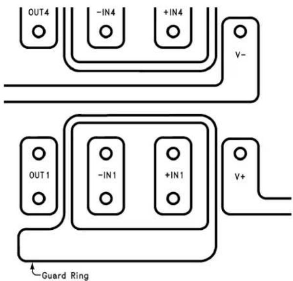
text_image
OUT4 -IN4 +IN4 V- OUT1 -IN1 +IN1 V+ Guard RingFigure78.ExampleofGuardRinginaPCBLayout
11DeviceandDocumentationSupport
11.1 DeviceSupport
FortheLMC6584PSpicemodel,seeSNOM165.
11.2 DocumentationSupport
11.2.1 Related Documentation
Forrelateddocumentation,seethefollowing:
• LMC6482 CMOS Dual Rail-To-Rail Input and Output Operational Amplifier data sheet
•LMC660CMOSQuadOperationalAmplifierdatasheet)
11.3SupportResources
TI E2E™ support forums are an engineer's go-to source for fast, verified answers and design help — straight fromtheexperts.Searchexistinganswersoraskyourownquestiontogetthequickdesignhelpyouneed.
Linked content is provided "AS IS" by the respective contributors. They do not constitute TI specifications and do not necessarily reflect TI's views; see TI's TermsofUse.
11.4 Trademarks
E2EisatrademarkofTexasInstruments.
Allothertrademarksarethepropertyoftheirrespectiveowners.
11.5ElectrostaticDischargeCaution

These devices have limited built-in ESD protection. The leads should be shorted together or the device placed in conductive foam during storage or handling to prevent electrostatic damage to the MOSgates.
11.6 Glossary
SLYZ022—TIGlossary.
This glossarylistsandexplainsterms,acronyms,anddefinitions.
12Mechanical, Packaging, and Orderable Information
The following pages include mechanical, packaging, and orderable information. This information is the most currentdataavailableforthedesignateddevices.Thisdataissubjecttochangewithoutnoticeandrevisionof thisdocument.Forbrowser-basedversionsofthisdatasheet,refertotheleft-handnavigation.
PACKAGING INFORMATION
| Orderable Device Status(1) | Package Type | Package Drawing | Pins | Package Qty | Eco Plan(2) | Lead finish/ Ball material(6) | MSL Peak Temp(3) | Op Temp (°C) | Device Marking(4-5) | Samples | |
| LMC6484AIM NRND SOIC D 14 55 Non-RoHS | Call TI Level-1-235C-UNLIM -40 to 85 LMC6484 | ||||||||||
| & Green | AIM | ||||||||||
| LMC6484AIM/NOPB ACTIVE SOIC D 14 55 RoHS & Green SN | Level-1-260C- UNLIM -40 to 85 LMC6484 | Samples | |||||||||
| AIM | |||||||||||
| LMC6484AIMX | NRND | SOIC | D | 14 | 2500 | Non-RoHS & Green | Call TI Level-1-235C-UNLIM -40 to 85 LMC6484 | ||||
| AIM | |||||||||||
| LMC6484AIMX/NOPB | ACTIVE | SOIC | D | 14 | 2500 | RoHS & Green | SN | Level-1-260C-UNLIM | -40 to 85 | LMC6484 AIM | Samples |
| LMC6484AIN/NOPB | ACTIVE | PDIP | N | 14 | 25 | RoHS & Green | Call TI | SN | Level-1-NA-UNLIM | -40 to 85 | LMC6484AIN | Samples |
| LMC6484IM | NRND SOIC D 14 55 Non-RoHS | Call TI Level-1-235C-UNLIM -40 to 85 LMC6484IM | |||||||||
| & Green | |||||||||||
| LMC6484IM/NOPB ACTIVE SOIC D 14 55 RoHS & Green SN Level-1-260C-UNLIM -40 to 85 LMC6484IM | Samples | ||||||||||
| LMC6484IMX NRND SOIC D 14 2500 Non-RoHS | Call TI Level-1-235C-UNLIM -40 to 85 LMC6484IM | ||||||||||
| & Green | |||||||||||
| LMC6484IMX/NOPB | ACTIVE | SOIC | D | 14 | 2500 | RoHS & Green | SN | Level-1-260C-UNLIM | -40 to 85 | LMC6484IM | Samples |
| LMC6484IN/NOPB | ACTIVE | PDIP | N | 14 | 25 | RoHS & Green | Call TI | SN | Level-1-NA-UNLIM | -40 to 85 | LMC6484IN | Samples |
(1) The marketing status values are defined as follows:
ACTIVE: Product device recommended for new designs.
LIFEBUY: TI has announced that the device will be discontinued, and a lifetime-buy period is in effect.
NRND: Not recommended for new designs. Device is in production to support existing customers, but TI does not recommend using this part in a new design.
PREVIEW: Device has been announced but is not in production. Samples may or may not be available.
OBSOLETE: TI has discontinued the production of the device.
(2) RoHS: TI defines "RoHS" to mean semiconductor products that are compliant with the current EU RoHS requirements for all 10 RoHS substances, Including the requirement that RoHS substance do not exceed 0.1% by weight in homogeneous materials. Where designed to be soldered at high temperatures, "RoHS" products are suitable for use in specified lead-free processes. TI may reference these types of products as "Pb-Free".
RoHS Exempt: TI defines "RoHS Exempt" to mean products that contain lead but are compliant with EU RoHS pursuant to a specific EU RoHS exemption.
Green: TI defines "Green" to mean the content of Chlorine (Cl) and Bromine (Br) based flame retardants meet JS709B low halogen requirements of <=1000ppm threshold. Antimony trioxide based flame retardants must also meet the <=1000ppm threshold requirement.
(3) MSL, Peak Temp. - The Moisture Sensitivity Level rating according to the JEDEC industry standard classifications, and peak solder temperature.
(4) There may be additional marking, which relates to the logo, the lot trace code information, or the environmental category on the device.
(5) Multiple Device Markings will be inside parentheses. Only one Device Marking contained in parentheses and separated by a "\~" will appear on a device. If a line is indented then it is a continuation of the previous line and the two combined represent the entire Device Marking for that device.
(6) Lead finish/Ball material - Orderable Devices may have multiple material finish options. Finish options are separated by a vertical ruled line. Lead finish/Ball material values may wrap to two lines if the finish value exceeds the maximum column width.
Important Information and Disclaimer: The information provided on this page represents TI's knowledge and belief as of the date that it is provided. TI bases its knowledge and belief on information provided by third parties, and makes no representation or warranty as to the accuracy of such information. Efforts are underway to better integrate information from third parties. TI has taken and continues to take reasonable steps to provide representative and accurate information but may not have conducted destructive testing or chemical analysis on incoming materials and chemicals. TI and TI suppliers consider certain information to be proprietary, and thus CAS numbers and other limited information may not be available for release.
In no event shall TI's liability arising out of such information exceed the total purchase price of the TI part(s) at issue in this document sold by TI to Customer on an annual basis.
TAPE AND REEL INFORMATION
*All dimensions are nominal
| Device Package | Type | Package Drawing | Pins | SPQ Reel | Diameter (mm) | Reel Width W1 (mm) | A0 (mm) | B0 (mm) | K0 (mm) | P1 (mm) | W (mm) | Pin1 Quadrant |
| LMC6484AIMX SOIC | D 14 2500 | 330.0 16 | 4 6.5 | 9.35 2.3 8.0 | 16.0 Q1 | |||||||
| LMC6484AIMX/NOPB SOIC | D 14 2500 | 330.0 16 | 16.4 | 6.5 9.35 2.3 | 8.0 16.0 | Q1 | ||||||
| LMC6484IMX SOIC | D 14 2500 | 330.0 16 | 4 6.5 | 9.35 2.3 8.0 | 16.0 | Q1 | ||||||
| LMC6484IMX/NOPB SOIC | D 14 2500 | 330.0 16 | 16.4 | 6.5 9.35 2.3 | 8.0 16.0 | Q1 |
text_image
TAPE AND REEL BOX DIMENSIONS W L*All dimensions are nominal
| Device | Package Type | Package Drawing | Pins | SPQ | Length (mm) | Width (mm) | Height (mm) |
| LMC6484AIMX SOIC | D 14 2500 367.0 367.0 35.0 | ||||||
| LMC6484AIMX/NOPB SOIC | D 14 2500 367.0 367.0 35.0 | ||||||
| LMC6484IMX SOIC | D 14 2500 367.0 367.0 35.0 | ||||||
| LMC6484IMX/NOPB SOIC | D 14 2500 367.0 367.0 35.0 |
TUBE
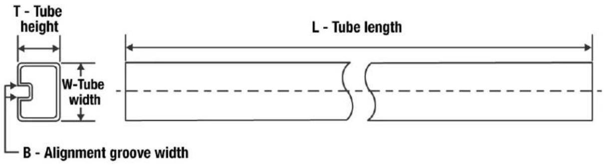
text_image
T - Tube height L - Tube length W-Tube width B - Alignment groove width*All dimensions are nominal
| Device | Package Name | Package Type | Pins | SPQ | L (mm) | W (mm) | T (μm) | B (mm) |
| LMC6484AIM D SOIC | 14 55 495 8 4064 | 3.05 | ||||||
| LMC6484AIM D SOIC | 14 55 495 8 4064 | 3.05 | ||||||
| LMC6484AIM/NOPB D | SOIC 14 55 495 8 4064 | 3.05 | ||||||
| LMC6484AIN/NOPB N | PDIP 14 25 502 14 | 11938 | 4.32 | |||||
| LMC6484IM | D SOIC 14 | 55 495 8 4064 | 3.05 | |||||
| LMC6484IM | D SOIC 14 | 55 495 8 4064 | 3.05 | |||||
| LMC6484IM/NOPB | D SOIC 14 | 55 495 8 4064 | 3.05 | |||||
| LMC6484IN/NOPB | N | PDIP | 14 | 25 | 502 | 14 | 11938 | 4.32 |
D (R-PDSO-G14)
PLASTIC SMALL OUTLINE

text_image
0.344 (8,75) 0.337 (8,55) 14 8 Pin 1 Index Area 1 0.050 (1,27) 7 0.244 (6,20) 0.228 (5,80) 0.157 (4,00) 0.150 (3,80) 0.020 (0,51) 0.012 (0,31) ⊕ 0.010 (0,25) M 0.069 (1,75) Max 0.010 (0,25) 0.004 (0,10) Gcuge Plane 0.010 (0,25) 0.005 (0,13) 0°-8° Seating Plane 0.010 (0,25) 0.050 (1,27) 0.016 (0,40) 4040047-5/M 06/11NOTES: A. All linear dimensions are in inches (millimeters).
B. This drawing is subject to change without notice.
Body length does not include mold flash, protrusions, or gate burrs. Mold flash, protrusions, or gate burrs shall not exceed 0.006 (0,15) each side.
Body width does not include interlead flash. Interlead flash shall not exceed 0.017 (0,43) each side.
E. Reference JEDEC MS-012 variation AB.
D (R-PDSO-G14)
4211283-3/E 08/12
NOTES: A. All linear dimensions are in millimeters.
B. This drawing is subject to change without notice.
C. Publication IPC-7351 is recommended for alternate designs.
D. Laser cutting apertures with trapezoidal walls and also rounding corners will offer better paste release. Customers should contact their board assembly site for stencil design recommendations. Refer to IPC-7525 for other stencil recommendations.
E. Customers should contact their board fabrication site for solder mask tolerances between and around signal pads.
N (R-PDIP-T\*\*)
16 PINS SHOWN
PLASTIC DUAL-IN-LINE PACKAGE
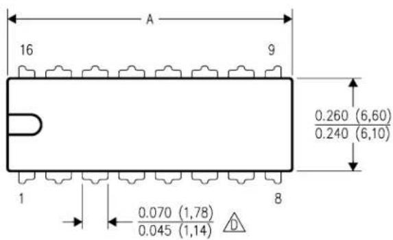
text_image
A 16 9 0.260 (6,60) 0.240 (6,10) 1 8 0.070 (1,78) 0.045 (1,14)C
| DIM\PINS ** | 14 | 16 | 18 | 20 |
| A MAX | 0.775(19,69) | 0.775(19,69) | 0.920(23,37) | 1.060(26,92) |
| A MIN | 0.745(18,92) | 0.745(18,92) | 0.850(21,59) | 0.940(23,88) |
| MS-001VARIATION | AA | BB | AC | AD |
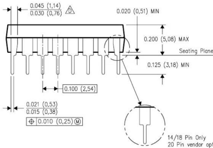
text_image
0.045 (1,14) 0.030 (0,76) D 0.020 (0,51) MIN 0.200 (5,08) MAX Seating Plane 0.125 (3,18) MIN 0.100 (2,54) 0.021 (0,53) 0.015 (0,38) ⊕ 0.010 (0,25) M 14/18 Pin Only 20 Pin vendor opt
text_image
0.325 (8,26) 0.300 (7,62) 0.015 (0,38) Gauge Plane 0.010 (0,25) NOM 0.430 (10,92) MAX4040049/E 12/2002
NOTES: A. All linear dimensions are in inches (millimeters).
B. This drawing is subject to change without notice.
C Falls within JEDEC MS-001, except 18 and 20 pin minimum body length (Dim A).
The 20 pin end lead shoulder width is a vendor option, either half or full width.
IMPORTANT NOTICE AND DISCLAIMER
TI PROVIDES TECHNICAL AND RELIABILITY DATA (INCLUDING DATA SHEETS), DESIGN RESOURCES (INCLUDING REFERENCE DESIGNS), APPLICATION OR OTHER DESIGN ADVICE, WEB TOOLS, SAFETY INFORMATION, AND OTHER RESOURCES "AS IS" AND WITH ALL FAULTS, AND DISCLAIMS ALL WARRANTIES, EXPRESS AND IMPLIED, INCLUDING WITHOUT LIMITATION ANY IMPLIED WARRANTIES OF MERCHANTABILITY, FITNESS FOR A PARTICULAR PURPOSE OR NON-INFRINGEMENT OF THIRD PARTY INTELLECTUAL PROPERTY RIGHTS.
These resources are intended for skilled developers designing with TI products. You are solely responsible for (1) selecting the appropriate TI products for your application, (2) designing, validating and testing your application, and (3) ensuring your application meets applicable standards, and any other safety, security, regulatory or other requirements.
These resources are subject to change without notice. TI grants you permission to use these resources only for development of an application that uses the TI products described in the resource. Other reproduction and display of these resources is prohibited. No license is granted to any other TI intellectual property right or to any third party intellectual property right. TI disclaims responsibility for, and you will fully indemnify TI and its representatives against, any claims, damages, costs, losses, and liabilities arising out of your use of these resources.
TI's products are provided subject to TI's Terms of Sale or other applicable terms available either on ti.com or provided in conjunction with such TI products. TI's provision of these resources does not expand or otherwise alter TI's applicable warranties or warranty disclaimers for TI products.
TI objects to and rejects any additional or different terms you may have proposed.
Mailing Address: Texas Instruments, Post Office Box 655303, Dallas, Texas 75265
Copyright © 2022, Texas Instruments Incorporated