SIM983 - Unspecified SRS - Free user manual and instructions
Find the device manual for free SIM983 SRS in PDF.

User questions about SIM983 SRS
0 question about this device. Answer the ones you know or ask your own.
Ask a new question about this device
Download the instructions for your Unspecified in PDF format for free! Find your manual SIM983 - SRS and take your electronic device back in hand. On this page are published all the documents necessary for the use of your device. SIM983 by SRS.
USER MANUAL SIM983 SRS
Revision2.3• January4,2016
Certification
StanfordResearchSystemscertifiesthatthisproductmetitspublishedspecificationsatthetime ofshipment.
Warranty
ThisStanfordResearchSystemsproductiswarrantedagainstdefectsinmaterialsandworkmanshipforaperiodofone(1)yearfromthedateofshipment.
Service
Forwarrantyserviceorrepair, thisproductmustbereturnedtoaStanfordResearchSystems authorizedservicefacility.ContactStanfordResearchSystemsoranauthorizedrepresentative beforereturningthisproductforrepair.
Informationinthisdocumentissubjecttochangewithoutnotice.
Copyright © StanfordResearchSystems, Inc., 2005–2016. All rights reserved.
StanfordResearchSystems, Inc.
1290-DReamwoodAvenue
Sunnyvale, CA94089USA
Phone:(408)744-9040• Fax:(408)744-9049
www.thinkSRS.com• e-mail:info@thinkSRS.com
PrintedinU.S.A.Documentnumber9-01598-903
Contents
GeneralInformationiii
SafetyandPreparationforUse......iii
Symbols......iv
Notation......v
Specifications......vi
1GettingStarted1-1
1.1 Introduction to the Instrument......1-2
1.2Front-PanelOperation....1-3
1.3Connections....1-5
1.4 Power-On 1-6
1.5RestoringtheDefaultConfiguration...... 1-6
1.6SIMInterface....1-7
2DescriptionofOperation
2.1 Signal Connections and Grounding ..... 2-2
2.2Autocalibration.... 2-2
2.3ACCharacteristics....2-3
2.4 Clock Stopping 2-4
3RemoteOperation
3.1IndexofCommonCommands.... 3-2
3.2 Alphabetic List of Commands 3-4
3.3 Introduction 3-6
3.4 Commands 3-7
3.5 Status Model 3-19
4PerformanceVerification
4.1 Verifying the DC Accuracy ..... 4-2
4.2 Verifying AC Performance.... 4-4
4.3 Noise Characteristics 4-6
4.4 Performance Test Record 4-8
5CircuitDescription
5.1 Circuit Discussion 5-2
5.2 Parts List 5-6
5.3 Schematic Diagrams 5-10
AIndexA-1
General Information
TheSIM983ScalingAmplifier, part of Stanford Research Systems' Small Instrumentation Modules family, perform the function
$$ V _ {\text { out }} = G \times (V _ {\mathrm{in}} + V _ {\mathrm{ofs}}) $$
where V_in and V_out are voltages (upto±10V) at the input and the output of the instrument, respectively, Gisauser-specified gain, and V_ofs is a user-specified offset voltage. The instrument is accurate within its resolution.
Safety and Preparation for Use
Thefront-panelinput, front-paneloutput, and therear-paneloutput coaxial(BNC) connectors in the SIM983 are referenced to the Earth, and their outercasings are grounded. Nodangerous voltages are generated by themodule.

CAUTION
Do not exceed ±15 volts to the Earth at the center terminal of each BNC connector. Donotinstallsubstitutepartsorperformunauthorized modificationstothisinstrument.
TheSIM983isasingle-widemodule designed to be used inside the SIM900Mainframe. Donotturnonthepower to themainframe or apply voltage input to the module until the module is completely inserted into themainframe and locked in place.
Symbols you may Find on SRS Products
| Symbol Description | |
 | Alternating current |
 | Caution - risk of electric shock |
 | Frame or chassis terminal |
 | Caution - refer to accompanying documents |
 | Earth (ground) terminal |
 | Battery |
 | Fuse |
| On (supply) | |
| Off (supply) | |
Notation

WARNING

CAUTION
The following notation will be used throughout this manual:
A warning mean that injury or death is possible if the instructions are not obeyed.
Acautionmeansthatdamagetotheinstrumentorotherequipment is possible.
Typesetting conventions used in this manual are:
- Front-panelbuttonsaresetas[gain]; [gain]isshorthandfor"[gain]&[gain]".
• Front-panelindicatorsaresetasOVLD.
• Signalnamesaresetas-STATUS.
• SignallevelsaresetasHIGH. - Remotecommandnamesaresetas*IDN?.
- Literaltextotherthancommandnamesissetas0FF.
• SpecialASCII charactersaresetas⟨CR⟩.
Remotecommandexampleswillallbesetinmonospacedfont. In these examples, datasentbythehostcomputertotheSIM983areset asstraightteletypefont, whileresponsesreceivedbythehost computerfromtheSIM983aresetasslantedteletypefont.
Specifications
Performance characteristics
| Input | Voltage [1] | MinTyp | MaxUnits | ||
| -10.0 | +10.0 | V | |||
| CouplingDC | |||||
| Resistance0 | 991.001.01 | MΩ | |||
| Capacitance2 | 6pF | ||||
| Biascurrent[2]40 | pA | ||||
| Voltagenoise[3,4],1kHz43nV/ | |||||
| 10kHz38nV/ | |||||
| Currentnoise,10kHz | 3 | fA/ | |||
| Terminals | GroundedBNC[5] | ||||
| Gain | Absolutevalue0.01 | 19.99 | |||
| Polarity | Inverting,non-inverting | ||||
| Resolution | 0.01 | ||||
| Accuracy[2]±0.01 | |||||
| Stability | ±10 | ppm/°C | |||
| Offset[3] | Voltage | -10.00 | +10.00 | V | |
| Resolution, |V_ofs| ≤ 1.999 V | 1 | mV | |||
| |V_ofs| ≥ 2.00 V10mV | |||||
| Accuracy [2,4,6] | ±1 ± 200 | mV + ppm | |||
| Stability [4] | ±20 ± 20 | ( V + ppm)/^ | |||
| Settlingtime[7] | 2 | s | |||
| AC performance | -3 dB bandwidth, |G| ≤ 1.00 | 2.0 | MHz | ||
| Gain-bandwidth product, |G| ≥ 1.00 | 3.0 | MHz | |||
| [8] |G| ≥ 2.40 | 5.0 | MHz | |||
| |G| ≥ 4.20 | 10.0 | MHz | |||
| |G| ≥ 9.60 | 17.0 | MHz | |||
| Slewrate70V/μs | |||||
| THD,1kHz | -90 | dB | |||
| Output | Voltage [1] | -10.0 | +10.0 | V | |
| Maximumcurrent | ±100 | mA | |||
| Shortcircuit duration | Indefinite | ||||
| Resistance50Ω | |||||
| Terminals | Grounded BNC, front [5] and rear [9] | ||||
| Operating | Temperature [10] | 0 | 40 | °C | |
| Power | +5, ±15 | V DC | |||
| Supply current, +5 V | 100 | mA | |||
| ±15V | 300 | mA | |||
Conditions:
[1] Anoverload will be detected and the instrument is not guaranteed to perform properly if these limits are exceeded, or if V_in + V_ofs exceeds the limits. Continuous application of an input voltage V_in in excess of ± 15V will damage the instrument.
[2]At23 °C.
[3]Referredtoinput.
[4]For|G| ≥ 2.
[5]Amphenol31-10-4052orsimilar.
[6]Followinganautocalibrationat(23±5) °Cwithin24hours;following a2-hourwarmup.
[7]Towithin0.1%ofthefinalvalue.
[8]Thegain-bandwidthproduct(GBP)determinesthe-3dBbandwidth: For gain G, the bandwidth is GBP/|G|.
[9]Tyco227169-4orsimilar.
[10]Non-condensing.
Generalcharacteristics
InterfaceSerial(RS-232)throughSIMinterface
ConnectorsBNC(2front[5],1rear[9]);DB-15(male)SIMinterface
Weight1.5lbs
Dimensions1.5 "W× 3.6 H× 7.0 D
1 Getting Started
Thischaptergivesyouthenecessaryinformationtogetstarted quicklywithyourSIM983ScalingAmplifier.
In This Chapter
1.1 Introduction to the Instrument......1-2
1.1.1 Frontandrearpanels......1–3
1.2Front-PanelOperation....1-3
1.2.1Polarity....1-3
1.2.2Gain....1-3
1.2.3Offset....1-4
1.2.4Overload....1-4
1.3Connections....1-5
1.4Power-On....1-6
1.5RestoringtheDefaultConfiguration .....1-6
1.6SIMInterface 1-7
1.6.1SIMinterfaceconnector......1-7
1.6.2 Directinterfacing......1–7
1.1 Introduction to the Instrument
TheSIM983ScalingAmplifierprovidesfineadjustablegainand offset control of an analog signal. The gain (0.01 ≤ |G| ≤ 19.99) , itspolarity(invertingornon-inverting), and the offset voltage (-10.00V ≤ V_ofs ≤ +10.00V) can be set from either the front panel or remotely. A remote computer can access the module through the SIM900Mainframe, using RS-232orGPIB.
ThedigitalcontrolcircuitryintheSIM983 is designed with aspecial clock-stopping architecture. Themicrocontrolleristurnedononly whenthepolarity, gain, or offset are being changed, during remote communications, or when an overload condition occurs. This guar- anteesthatnodigitalnoisecontaminateslow-levelanalogsignals.
DC accuracy A user-commanded autocalibration procedure allows one to control theinput-referredoffsettowithin±1mVofthedesiredvalue.
The amplifier's high slew rate allows it to output a ±10 V peak-peak sine wave at a frequency of 1 MHz. The gain stage of the amplifier is compensated in a flexible fashion to provide an sensible pulsere-sponse, so the bandwidth of the instrument is adjusted according to its gain. ^1 The ample output current in the SIM983 permit soneto drive a 50Ω load.
If the maximum input voltage is exceeded, or the gain or offset cause the output voltage to exceed its maximum, the appropriate overload LEDturnson. If armed, themodulealsogeneratesastatussignalto alert the user of the overload condition. The SIM983 can be operated outsidetheSIM900MainframebypoweringitwithitsrequiredDC voltages.
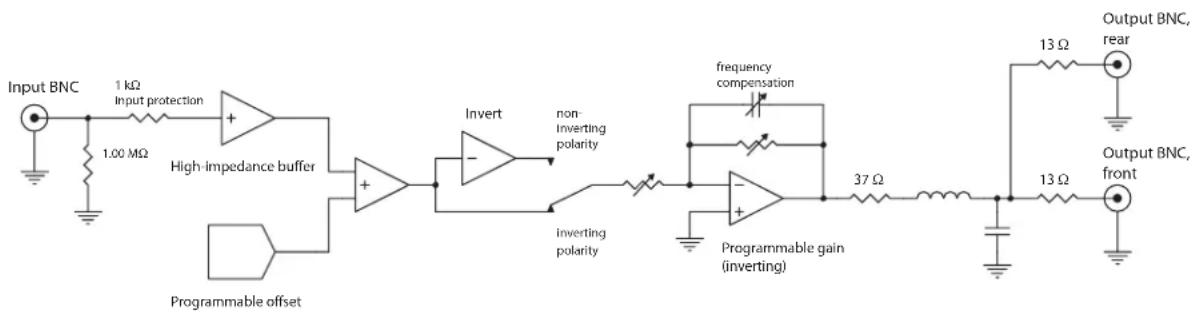
AblockdiagramoftheamplifierisshownbelowinFigure 1.1.
flowchart
graph TD
    A["Input BNC"] --> B["1.00 MΩ"]
    B --> C["High-impedance buffer"]
    C --> D["Programmable offset"]
    D --> E["Invert"]
    E --> F["non-inverting polarity"]
    F --> G["Programmable gain (inverting)"]
    G --> H["37 Ω"]
    H --> I["Output BNC, rear"]
    G --> J["13 Ω"]
    G --> K["13 Ω"]
    L["Programmable gain (inverting)"] --> M["frequency compensation"]
    M --> N["Inverting polarity"]
    N --> O["Inverting polarity"]
    O --> P["Inverting polarity"]
    P --> Q["Inverting polarity"]
    Q --> R["Inverting polarity"]
    R --> S["Inverting polarity"]
    S --> T["Inverting polarity"]
    T --> U["Inverting polarity"]
    U --> V["Output BNC, front"]
Figure 1.1:TheSIM983blockdiagram.
1.1.1 Front and rear panels

text_image
VSRS SIM983 Scaling Amplifier Gain 15.75 Input Offset -.090 polarity gain offset INPUT OVLD 1 MΩ OUTPUT OVLD ±10 V SIM983 SCALING AMP OUTPUT S/N VSRS MADE IN U.S.A.Figure1.2:TheSIM983frontandrearpanels.
1.2 Front-Panel Operation
1.2.1 Polarity
Thepolarityisthesignofthegain.Itisindicatedontheupperdisplay ofthefrontpanel.Tochangethepolarity,pressthe[polarity]button once.Holdingthisbuttonhasnoeffect.
Pressing[polarity]hasnoeffectontheinput-referredoffset.However,asimultaneous pressof[polarity]andoneof[gain]hasa specialmeaning.Thispressinitiatesautocalibration(Section2.2).
1.2.2 Gain
ThegainGcanbesettoanabsolutevaluebetween0.01and19.99.To raiseorlowertheabsolutevalueofthegain,pressthebutton[gain] orthebutton[gain]. Thedecimalpointpositionofthegaindisplayedonthefrontpanelisfixed,sotheresolutionofthegainis0.01. If [gain 1] is pressed when the gain G = ± 19.99 , the press has no effect. If [gain 7] is pressed when G = ± 0.01 , the press has no effect. Pressing either [gain] does not change the polarity.
Ifoneof[gain]ispressedandheld, thegainiscontinuouslyadjusted. Therateoftheadjustmentincreasesasthebuttonisheld. If theabsolutevalueofthegainisbeinglowered, therateoftheadjustment changes as |G| crosses 1.00, and possibly again as |G| crosses 0.10.
resetting gain
If both [gain ▲] and [gain ▼] buttons are pressed at the same time, the absolute value of the gain is reset to 1.00. This action does not change the polarity.
Pressingoneof[gain]and[polarity]atthesametimehasaspecial meaning. Thispressinitiatesautocalibration(Section2.2).
1.2.3 Offset
The input-referred voltage offset V_ofs can be set to a value between -10.00 V and +10.00 V. Its value, in volts, is shown on these second line of display on the front panel of the amplifier.
To increase or decrease the offset, press the button [offset ▲] or the button [offset ▼]. Unlike the gain, the “up” and “down” buttons adjust the offset, not its absolute value. Thus, for example, pressing [offset ▲] when V_ofs = -5.49V makes V_ofs = -5.48V . If [offset ▲] is pressed when V_ofs = +10.00V , the press has no effect. If [offset ▼] is pressed when V_ofs = -10.00V , the press has no effect.
Between the values -2.00V < V_ofs < +2.00V , the offset is selected with 0.001V resolution; the position of the decimal point on the front-panel display is shifted to the left. Although the resolution is 0.01V for |V_ofs| ≥ 2.00V , the accuracy of the offset is still ± 1mV ± 0.02% . Thus, for example, setting V_ofs = -5.48V produces V_ofs = (-5.480 ± 0.001 ± 0.001) = (-5.480 ± 0.002)V .
If one of [offset ▲] is pressed and held, the offset is continuously adjusted. Therateoftheadjustmentincreasesasthebuttonisheld. If the valuecrossesthethreshold V_ofs = ± 2.00 V , the rate changes appropriately.
resetting offset
If both [offset ▲] and [offset ▼] buttons are pressed at the same time, the offset is reset to 0.000 V.
1.2.4 Overload
There are two overload indicators, one OVLD LED in the INPUTblockandoneOVLD LEDintheOUTPUTblockofthefront panel. The overload signal can also be asserted on the STATUS pin. SeeSection3.5.
1.2.4.1 Input overload
AnoverloadconditionisrecognizedandtheinputOVLDLEDis activatediftheabsolutevalueofthevoltageappliedtotheinput overload limits exceeds certain limits. These limits are typically ±10.0 V, and are between
$$ - 1 0. 4 \mathrm{V} \leq V _ {\min} \leq - 9. 9 \mathrm{V}, 9. 9 \mathrm{V} \leq V _ {\max} \leq 1 0. 4 \mathrm{V}. $$
Theoverloadedstateisalsorecognized,andtheinputoverloadLED activated,ifthesumoftheinputvoltageandthecommandedoffset, |V_in+V_ofs| , exceeds these limits. To distinguish between the two input overloadpossibilities,usethecommandOVLD? .TheoverloadLED staysonforaminimumof50ms; afterthistimeitturnsoffithe overloadconditionhasceased.
1.2.4.2 Output overload
AnoverloadconditionisrecognizedandtheoutputOVLD LEDis activated if the absolute value |G × (V_in + V_ofs)| exceeds the limits in Section 1.2.4.1. The overload LED stays on for a minimum of 50 ms; afterthistimeitturnsoffiftheoverloadconditionhasceased.
1.3 Connections
For a discussion of the front and rear BNC connections, see Section2.1.TheSIMinterfaceconnectorisdiscussedinSection1.6.1.
1.4 Power-On
The instrument retains the values of the gain and the offset inn non-volatile memory. Upon power-on, those settings are restored to their values before the power was turned off.
The power-on configuration of theremote interface is detailed in Section 3.3.1.
1.5 Restoring the Default Configuration
The default configuration of the SIM983 is G = +1.00 , V_ofs = 0.000V , and bandwidth@(seeSection2.3.1). This configuration is reached from theremote interface by issuing the *RST command. To reset only the gain the offset to their default values, use button combinations described in Sections 1.2.2 or 1.2.3.
1.6 SIM Interface
The primary connection to the SIM983 Scaling Amplifier is therear-panel DB-15 SIM interface connector. Typically, the SIM983 is mated to a SIM900 Mainframe viathis connection, either throughout one of the internal mainframeslots or theremotecable interface.
ItisalsopossibletooperatetheSIM983directly, without using the SIM900Mainframe. Thissectionprovidesdetailsontheinterface.
1.6.1 SIM interface connector
TheDB-15SIMinterfaceconnectorcarriesallthepowerandcommunicationlinestotheinstrument.Theconnectorsignalsarespecified inTable1.1.
| Pin | SignalSrc | DestDescription | Direction | |
| 1 | S | IGNALGNDMF | SIM GroundReference1 | |
| 2 | -STATUS | SIM MF | Status/service request (GND = asserted, +5 V= idle) | |
| 3 | RTS | MF SIM | HW handshake (unused in SIM983) | |
| 4 | CTS | SIM MF | HW handshake (unused in SIM983) | |
| 5 | -REF_10MHZ | MF SIM | 10 MHz reference (no connection in SIM983) | |
| 6 | -5V | MF SIM | Power supply (no connection in SIM983) | |
| 7 | -15V | MF SIM | Power supply | |
| 8 | PSRTN | MF SIM GroundReference2 | ||
| 9 | CHASSISGND Chassisground | |||
| 10 | TXD | MF SIM | Async data (start bit = “0”= +5 V; “1”= GND) | |
| 11 | RXD | SIM MF | Async data (start bit = “0”= +5 V; “1”= GND) | |
| 12 | +REF_10MHZ | MF SIM | 10 MHz reference (no connection in SIM983) | |
| 13 | +5V | MF SIM | Power supply | |
| 14 | +15V | MF SIM | Power supply | |
| 15 | +24V | MF SIM | Power supply (no connection in SIM983) | |
Table1.1: SIMinterfaceconnectorpinassignments,DB-15.
1.6.2 Direct interfacing
TheSIM983isintendedforoperationintheSIM900Mainframe, but usersmaywishtodirectlyinterfacethemoduletotheirownsystems withouttheuseofadditionalhardware.
ThematingconnectorneededisastandardDB-15receptacle,such asTycopartnumber747909-2(orequivalent).Clean,well-regulated supply voltages of ± 15.0V DC, +5.0V DC must be provided, followingthepinoutspecified inTable1.1 andtheminimumcurrentsin thetableonPagevi.GroundmustbeprovidedonPins1and8,with chassis ground on Pin 9. The STATUS signal may be monitored

CAUTION
onPin2foralow-goingTTL-compatibleoutputindicatingastatus message.SeeSection3.5forthedescriptionofstatusmessages.
The SIM983 has nointernal protection against reverse polarity, missing supply, or overvoltage on the +5 V and the ±15 V power-supply pins. Supply voltages above 5.5 V on Pin 13, above +16 V on Pin 14, or below -16 V on Pin7 are likely todamagethe instrument. SRS recommends using the SIM983 together with the SIM900 Mainframe form most applications.
1.6.2.1 Direct interface cabling
If the user intend stodirectly wire the SIM983 independent of the SIM900 Mainframe, communication is usually possible by directly connecting the appropriate interfacelines from the SIM983 DB-15 plug to the RS-232 serial port of a personal computer. ^2 Connect RXD from the SIM983 directly to R Don the PC, TX D directly to TD, and similarly RTS→RT Sand CTS→CTS. In other words, anull-modem-styleable is not needed.
TointerfacedirectlytotheDB-9male(DTE)RS-232porttypically foundoncontemporarypersonalcomputers,acablemustbemade withafemaleDB-15sockettomatewiththeSIM983,andafemale DB-9sockettomatewiththePC'sserialport.Separateleadsfrom theDB-15needtogotothepowersupply,makingwhatissometimes knowasa"hydra"cable.ThepinconnectionsaregiveninTable1.2.
DB-15/FtoSIM983Name
| DB-9/F | ||
| 10←→ | 3 | TxD |
| 11←→ | 2 | RxD |
| 5 | ComputerGround | |
| toPowerSupply | ||
| 7←→ | -15VDC | |
| 13←→ | +5 V DC | |
| 14←→ | +15 V DC | |
| 1←→ | Ground 1 (separate wire to Ground) | |
| 8←→ | Ground 2 (separate wire to Ground) | |
| 9←→ | Chassis Ground (separate wire to Ground) | |
Table1.2:SIM983directinterfacecablepinassignments.
note about grounds The distinct Ground References 1 and 2, and the chassis ground, are not directly connected within the SIM983. Ground1carriesthereturn
currentsofdigitalcontrolsignalsandthepowersupplies,whereas theinputvoltageandtheoutputvoltagereferencetoGround2(Section2.1.2).WhenoperatingintheSIM900,thethreegroundsare tiedtogetherintheSIM900Mainframe.Grounds1and2areconnectedthroughback-to-backSchottkydiodes,sotheycannotbemore than ±0.35 V apart. The three ground lines should be separately wiredtoasingle,low-impedancegroundsourceatthepowersupply.
1.6.2.2 Serial settings
The initial serial port settings at power-on are: baud rate 9600, 8 bits, n parity, 1 stop bit, and no flow control. The baud rate of the SIM 983 cannot be changed. Flow control is not implemented in the SIM 983. The parity may be changed with the PARI command.
2 Description of Operation
Thischapterprovidesanumberofadditionaldetailsoftheoperation oftheSIM983.
In This Chapter
2.1SignalConnectionsandGrounding......2-2
2.1.1 Outputdrive....2-2
2.1.2 Grounds....2-2
2.2Autocalibration....2-2
2.3ACCharacteristics....2-3
2.3.1 Bandwidth....2-3
2.3.2Slewrate....2-3
2.4ClockStopping......2-4
2.1 Signal Connections and Grounding
2.1.1 Output drive
The output impedance of the SIM983 Scaling Amplifier is 50Ω. The amplifier and drivelo load impedances from ∞ to 50Ω for the full ±10V range of output voltage. When driving a 50Ω load, the gain will be half of that displayed on the front panel.
Therear-paneloutputconnectoriswiredinparallelwiththefrontpaneloutput, and share some of the output impedance (Figure 1.1). The output stage is not designed to drivetwo 50 loadssimultaneously.
2.1.2 Grounds
Both the input and the output of the SIM983 are referenced to ground. Tomaintain the DC accuracy of the instrument, there are two separate ground references. Ground1 (Pin1 of the SIM interface connector) provides a return path for digital control signals and the power supply currents, while Ground2 (Pin8 of the interface connector) serves as there reference point for analog voltages. The outercasings of the input and the output front-panel BNC connectors are tied to Ground2. The output current of the amplifier return to the power supply through Ground2.
The outercasing of therear-panel output BNC is connected to chassis ground, Pin9 of the DB-15 SIM interface connector. These separate power, analog, and chassis grounds are not directly connected within the amplifier. When operating in the SIM 900 Mainframe, the three grounds are tied together inside them mainframe, and through them in frameto the Earth. Grounds 1 and 2 are connected inside the SIM 983 through back-to-back Schottky diodes, so they cannot be more than ±0.35 V apart.
2.2 Autocalibration
ToensureDCoffsetaccuracy, theamplifiermustbeself-calibrated within the 24 hours preceding a measurement. A valid autocalibrationmusttakeplaceat(23±5) °C with themodulewarmedup for at least 2 hours at (23±5) °C. If the module is being used inside the SIM900Mainframe, theautocalibration must also be inside themainframe. Otherwise, perform theautocalibration with the same connection to an independent supply as you use for the operation. Theautocalibration is only accurate if the output has stabilized within ±15 mV of zero for at least 2 minutes immediately preceding the calibration. However, the gain and the offset need not be at
theirdefaultvalues;afterthecalibrationcompletes,thesevaluesare restored.
DisconnectallinputsandoutputstotheSIM983whileperformingtheautocalibration.Tocalibrate,issuethecommandACAL,orpressthebutton[polarity]andoneof[gain]atthesametime.Thecalibration completesandtheinstrumentisreadyforoperationwithin2seconds.Ifautocalibrationisunsuccessful,forexamplebecausean externalvoltage(whichcannotbenulled)isappliedtotheinput,the calibrationparametersreverttotheiroriginalvaluesandthecommandLDDE? willreturnCode1.
Autocalibrationdoesnotaffectgainaccuracy.
2.3 AC Characteristics
2.3.1 Bandwidth
Thegain-bandwidthproduct(GBP)oftheSIM983isameasureof its small-signal behavior, and depends on |G| . Four gain ranges correspondtofourvaluesofgain-bandwidthproduct, aspecified in the table on Page vi. For |G| ≥ 1 , the -3 dB small-signal bandwidth of the amplifier is f_-3dB = GBP / |G| . For |G| < 1 , f_-3dB(G) f_-3dB(G = 1.00) .
Thegain-bandwidthproductisdeterminedbyacompensationcapacitorinthefeedbackpathofthegain-stageamplifier.Itispossible tooverridethevalueofthiscapacitor,givingtheinstrumentmore bandwidth.Todothis,usethecommandBWTH.Ifthebandwidth isalteredinthisway,thenextfront-panelbuttonpresswillreturn the bandwidth to the value appropriate for the current gain. Cyclingthepowerorperforminganautocalibrationwillalsoreturnthe bandwidthtoitsdefaultvalueforthegain.
Ifthebandwidthissettoavalueotherthanitsdefault,theamplifiermayexhibitslowsettling,excessiveringing,oroscillations.
Thesmall-signalsettlingtimeoftheamplifierisacomplexfunction ofitsgainanditsbandwidth.
2.3.2 Slew rate
The slew rate of an amplifier is a measure of its large-signal behavior. It is the maximum rate of change of the output voltage, measured in V/s. The slew rate (SR) determines the maximum undistorted AC signal that can be output; forasine-wave output at a frequency f, the maximum peak-peak voltage is |V_-V_| = SR/( f) . The SIM983 is designed to be able to output a full-rangesinewave at 1 MHz.
If the outputor an intermediate stage of the amplifier is driven beyond the limits in the table on Pagevi, large-signal behavior is not guaranteed.
2.4 Clock Stopping
ThemicroprocessorclockoftheSIM983stopsifthemoduleisidle, "freezing"thedigitalcircuitry.Thefollowingactions"wakeup"the clock:
- Apower-on.
- Apressofafront-panelbutton.
3.Activity(sendorreceive)attheremoteinterface. - Anoverload.
Theclockrunsforaslongasisnecessarytocompleteagainoroffset adjustment,ortocommunicatetheoutputofaquerythroughthe remoteinterface.However,theclockwillremainactiveforaslong astheoverloadconditionexists.
This default behavior can be modified with the remote command AWAK. Setting AWAK ON will prevent the clock from stopping. The module returns to AWAK OFF upon power-on.
3 Remote Operation
ThischapterdescribesoperatingtheSIM983overtheserialinterface.
In This Chapter
3.1IndexofCommonCommands......3-2
3.2AlphabeticListofCommands......3-4
3.3Introduction....3-6
3.3.1 Power-onconfiguration......3-6
3.3.2Buffers....3-6
3.3.3DeviceClear....3-6
3.4Commands....3-7
3.4.1 Commandsyntax....3-7
3.4.2 Notation....3-8
3.4.3Examples....3-8
3.4.4 General commands....3-9
3.4.5Configurationcommands......3-10
3.4.6 Calibration commands....3-11
3.4.7Statuscommands....3-11
3.4.8Interfacecommands....3-14
3.4.9 Serialcommunicationcommands.....3-17
3.5 Status Model 3-19
3.5.1StatusByte(SB)....3-20
3.5.2ServiceRequestEnable(SRE)......3-20
3.5.3 StandardEventStatus(ESR)......3-20
3.5.4 StandardEventStatusEnable(ESE).....3-21
3.5.5CommunicationErrorStatus(CESR).....3-21
3.5.6CommunicationErrorStatusEnable(CESE)3-22
3.5.7OverloadStatus(OLSR)......3-22
3.5.8OverloadStatusEnable(OLSE)......3-23
3.1 Index of Common Commands
SymbolDefinition
fFloating-pointvalue
iBitnumber(0–7)
jUnsignedinteger(0-255)
mUnsignedinteger(0-3)
zLiteraltoken
(?) Requiredforqueries;illegalforsetcommands
varParameteralwaysrequired
{var} Requiredparameterforsetcommands;illegalforqueries
[var]Optionalparameterforbothsetandqueryforms
General
HELP(?) 3–9InstrumentHelp
AWAK(?) {z} 3 - 10 Keep Clock Awake
Configuration
GAIN(?) {f} 3-10 Gain
OFST(?) {f} 3-10 Offset
BWTH(?) [m] 3-11 Bandwidth
Calibration
ACAL 3–11 Autocalibration
Status
*CLS 3-11 ClearStatus
*STB? [i] 3-12 Status Byte
*SRE(?) [i,] {j} 3 - 12 Service Request Enable
*ESR? [i] 3 – 12 Standard Event Status
*ESE(?) [i,] {j} 3-12 Standard Event Status Enable
CESR? [i] 3-12 Communication Error Status
CESE(?) [i,] {j} 3-13 Communication Error Status Enable
OLSR? [i] 3-13 Overload Status
OLSE(?) [i,] {j} 3-13 Overload Status Enable
PSTA(?) {z} 3-13 Pulse STATUS Mode
LBTN? 3-13 LastButton
OVLD? 3-14 Overload
Interface
*RST 3-14 Reset
*IDN? 3–15 Identify
*TST? 3 – 15 Self Test
*OPC(?) 3-15OperationComplete
CONS(?) {z} 3-15 Console Mode
LEXE? 3-16ExecutionError
LCME? 3-16CommandError
LDDE? 3-17DeviceError
TOKN(?) {z} 3-17 Token Mode
TERM(?) {z} 3-17 Response Termination
Serial Communications
PARI(?) {z} 3-18 Parity
3.2 Alphabetic List of Commands
★
*CLS 3-11ClearStatus
*ESE(?) [i,] {j} 3-12 Standard Event Status Enable
*ESR? [i] 3–12StandardEventStatus
*IDN? 3–15Identify
*OPC(?) 3-15OperationComplete
*RST 3-14Reset
*SRE(?) [i,] {j} 3-12 Service Request Enable
*STB? [i] 3–12StatusByte
*TST? 3–15SelfTest
A
ACAL 3–11 Autocalibration
AWAK(?) {z} 3-10 Keep Clock Awake
B
BWTH(?) [m] 3-11 Bandwidth
C
CESE(?) [i,] {j} 3-13 Communication Error Status Enable
CESR? [i] 3-12 Communication Error Status
CONS(?) {z} 3-15 Console Mode
G
GAIN(?) {f} 3-10 Gain
H
HELP(?) 3–9 InstrumentHelp
L
LBTN? 3-13LastButton
LCME? 3-16CommandError
LDDE? 3-17DeviceError
LEXE? 3-16ExecutionError
0
OFST(?) {f} 3-10 Offset
OLSE(?) [i,] {j} 3-13 Overload Status Enable
OLSR? [i] 3-13 Overload Status
OVLD? 3-14Overload
P
| PARI(?) {z} | 3-18 Parity |
| PSTA(?) {z} | 3-13 Pulse ¬STATUS Mode |
T
| TERM(?) {z} | 3-17 Response Termination |
| TOKN(?) {z} | 3-17 Token Mode |
3.3 Introduction
RemoteoperationoftheSIM983istroughasimplecommandlanguagedocumentedinthischapter.Bothsetandqueryformsofmost commandsaresupported,allowingtheusercompletecontrolofthe amplifierfromaremotecomputer,eitherthroughtheSIM900MainframeordirectlyviaRS-232(seeSection1.6.2.1).
SeeTable1.1forthespecificationoftheDB-15SIMInterfaceConnector.
3.3.1 Power-on configuration
The initial settings for theremote interface are 9600 baud with no parity and no flow control, and with locale chodisabled (CONS OFF).
The values of the gain and the offsetarer retained in non-volatile memory. Upon power-on, those settingsarer restored to their values before the power wasturned off. The bandwidth this set to the value appropriate for the stored gain.
Whereappropriate, thedefaultorpower-onvalueforparametersis listedinboldfaceinthecommanddescriptions.
3.3.2 Buffers
TheSIM983storesincomingbytesfromthehostinterfaceina64-byteinputbuffer.Charactersaccumulateintheinputbufferuntil a command terminator (either CR or LF ) is received, at which pointthemessageis parsed and executed.Queryresponsesfrom theSIM983arebufferedina64-byteoutputqueue.
If the input buffer overflows, then all data in both the input buffer and the output queue are discarded, and an error is recorded in the CESRandESRstatus registers.
3.3.3 Device Clear
TheSIM983hostinterfacecanbeasynchronouslyresettoitspower-onconfigurationbysendinganRS-232-style
TheDeviceClearsignalwillalsoterminatetheoutputoftheHELP?commandfromtheSIM983.
3.4 Commands
Thissectionprovidessyntaxandoperationaldescriptionsforremote commands.
3.4.1 Command syntax
The four letter mnemonic (shown in CAPS) in each command sequence specifies the command. Therest of these sequence consists of parameters.
Commandsmaytakeeithersetorqueryform,dependingonwhether the“?”characterfollowsthemnemonic.Setonlycommandsare listed without the “?”, query only commands show the “?” after the mnemonic,andoptionallyquerycommandsaremarkedwitha“(?)”.
Parametersshownin{ } and[]arenotalwaysrequired.Parameters in{ } arerequiredtosetavalue,andshouldbeomittedforqueries.Parametersin[]areoptionalinbothsetandquerycommands.Parameterslistedwithoutsurroundingcharactersarealwaysrequired.
Donotsend()or{ } or[]aspartofthecommand.
Multipleparametersareseparatedbycommas.Multiplecommands maybesentononecommandlinebyseparatingthemwithsemicolons(;)solongastheinputbufferdoesnotoverflow.Commands are terminated by either CR or LF characters. Null commands andwhitespacesareignored.Executionofthecommanddoesnot beginuntilthecommandterminatorisreceived.
tokens Token parameters (generically shown as z in the command descriptions) can be specified either as a key word or an integer value. Command descriptions list the valid keyword options, with each keyword followed by its corresponding integer value. Forexample, to set the response termination sequence to CR + LF , the following two commands are equivalent:
TERM CRLF —or— TERM 3
Forqueriesthatreturntokenvalues,thereturnformat(keywordor integer)isspecifiedwiththeTOKN command.
3.4.2 Notation
The following tables summarize the notation used in the command descriptions:
SymbolDefinition
fFloating-pointvalue
iBitnumber(0–7)
jUnsignedinteger(0–255)
mUnsignedinteger(0-3)
zLiteraltoken
(?) Requiredforqueries;illegalforsetcommands
varParameteralwaysrequired
{var} Requiredparameterforsetcommands;illegalforqueries
[var]Optionalparameterforbothsetandqueryforms
3.4.3 Examples
Each command is provided with a simple example illustrating its usage. In these examples, all data sent by the host computer to the SIM983 are set as straight teletype font, while responses received by the host computer from the SIM983 are set as slanted teletype font.
The usage examples vary with respect to query, optional parameters, and token formats. These examples are not exhaustive, and are intended to provide a convenient starting point for user programming.
3.4.4 General commands
InstrumentHelpHELP(?)
OutputsacondensedversionofSection3.4totheremoteinterface.
HELP maybeusedwithorwithoutthequerysign,withthesame effects.
HELP?Example:
Notation:
fisafloating-pointnumber;
iisbitnumber(0..7);
jisan8-bitunsignedinteger(0..255);
misa2-bitunsignedinteger(0..3);
zisatoken
(?)questionrequiredforqueries,illegalforsetcommands;
[]=parameterisoptionalforbothsetandqueryforms;
{}=parameterisrequiredtoset,illegalforqueries;
parameterwithoutbracketsisalwaysrequired;
thebracketsthemselvesshouldnotbesent.
General commands:
HELP?-Sendthistext.
AWAK(?) {z}-Keepthemoduleclockawake.
Configurationcommands:
GAIN(?) {f}-Set/querygain.
OFST(?) {f}-Set/queryoffset.
BWTH(?) [m]-Outputbandwidth.
Calibrationcommands:
ACAL-One-timeautocalibration.
Statuscommands:
*CLS-ClearStatus.
*STB?[i]-QuerytheStatusByte.
*SRE(?) [i, ] {j} -ServiceRequestEnable.
*ESR?[i]-QueryStandardEventStatusregister.
*ESE(?) [i, ] {j} - StandardEventStatusEnable.
CESR?[i]-QuerytheCommunicationsErrorStatus.
CESE(?) [i, ] {j} - CommunicationsErrorStatusEnable.
OLSR?[i]-QueryOverloadStatusregister.
OLSE(?) [i, ] {j} -OverloadStatusEnable.
PSTA(?){z}-PulseStatusorchangeitslevel.
LBTN?-Whichbuttonlastpressed?
OVLD?-Inputoroutputcurrentlyoverloaded?
| Interfacecommands:*RST-Resettoknownstate.*IDN?-Identify.*TST?-Doesnothing.*OPC(?)-Operationcomplete.CONS(?){z}-ConsoleOFF/ON.LEXE?-LastExecutionError.LCME?-LastCommunicationsError.LDDE?-LastDevice-DependentError.TOKN(?){z}-TurntokenmodeOFF/ON.TERM(?){z}-Cmdlineend(NONE,CR,LF,CRLF,LFCR).Serialinterfacecommand(baudrateisalways9600):PARI(?){z}-Parity(NONE,EVEN,ODD,MARK,SPACE). | |
| AWAK(?) {z} | Keep Clock AwakeSet (query) the SIM983 keep-awake mode {to z = (OFF 0, ON 1)}.Ordinarily, the clock oscillator for the SIM983 microcontroller is held in a stopped state, and only enabled during processing of events (Section 2.4). Setting AWAK ON forces the clock to stay running, and isusefulonlyfordiagnosticpurposes. |
| Example: | AWAKON |
3.4.5 Configuration commands
| GAIN(?) {f} | Gain |
| Set (query) the amplifier gain {to f}. The module accepts signed floating-point values in the ranges -19.99 ≤ f ≤ -0.01, 0.01 ≤ f ≤ 19.99 . The reset value is f = +1.00 . | |
| AfteraGAIN setcommand,thebandwidthissettothevalueappropriateforthenewgain.Gainqueriesdonotalterthebandwidth. | |
| Example: | GAIN1.4232E1;GAIN?+14.23 |
| OFST(?) {f} | Offset |
| Set (query) the offset of the amplifier {to f volts}. The module accepts signed floating-point values in the range -10.000 ≤ f ≤ 10.000 . The reset value is f = 0.000 . | |
| Settingorqueryingtheoffsetdoesnotchangethebandwidth. |
OFST-7.032;OFST?Example: -07.030
BandwidthBWTH(?) [m]
Set(query)thegain-bandwidthproductoftheamplifier[tom].Allowedvaluesoftheoptionalparameterare0through3,withalarger valuecorrespondingtoagreatergain-bandwidth. Whenthegainis setfromthefrontpanelorfromtheremoteinterface,thebandwidth automaticallyrevertstothefollowing:
RangeBandwidthmGBP,MHzmin
| 0.01 ≤ |G| ≤ 2.39 | 0 | 3.0 (|G| ≥ 1.00) |
| 2.40 ≤ |G| ≤ 4.19 | 1 | 5.0 |
| 4.20 ≤ |G| ≤ 9.59 | 2 | 10.0 |
| 9.60 ≤ |G| ≤ 19.99 | 3 | 17.0 |
The bandwidth is also automatically selected from this table if the optionalparameterisomitted.
Example: GAIN17; BWTH1; BWTH?
1
GAIN17; BWTH?
3
3.4.6 Calibration commands
| ACAL | AutocalibrationPerform a self-calibration (Section 2.2). Make sure to disconnect all inputsandoutputstotheSIM983,andtosettheoutputtozero.Remote commands are not processed until ACAL is complete. |
| Example: ACALLDDE?0checksforsuccessofanautocalibration. |
3.4.7 Status commands
TheStatuscommandsqueryandconfigureregistersassociatedwith statusreportingoftheSIM983. SeeSection3.5forthestatusmodel.
*CLS ClearStatus *CLS immediatelyclearstheESR,CESR,andOLSRstatusregisters. Example: *CLS
| StatusByte*STB? [i]QuerytheStatusByteregister[Biti].Executionofthe*STB? query(withouttheoptionalBiti)always causes the ¬STATUS signal to be deasserted. Note that *STB? i will not clear ¬STATUS, even if Bit i is the only bit presently causing the ¬STATUSsignal.*STB?Example:16 | |
| *SRE(?) [i,] {j} | Service Request EnableSet (query) the Service Request Enable register [Bit i] {to j}.*SRE0, 1Example: |
| StandardEventStatus*ESR? [i]QuerytheStandardEventStatusRegister[Biti].Uponexecutionof*ESR?,thereturnedbit(s)oftheESRregisterare cleared.*ESR?Example:64 | |
| *ESE(?) [i,] {j} | Standard Event Status EnableSet (query) the Standard Event Status Enable register [Bit i] {to j}.*ESE6, 1Example:ESE?64 |
| CESR? [i] | Communication Error StatusQuerytheCommunicationErrorStatusRegister[Biti].UponexecutingaCESR? query,thereturnedbit(s)oftheCESRregisterarecleared.CESR?Example:0 |
| CESE(?) [i,] {j} | Communication Error Status EnableSet(query)theCommunicationErrorStatusEnableregister[Biti]{toj}.CESE?Example:2 |
| OverloadStatusOLSR? [i]QuerytheOverloadStatusRegister[Biti].UponexecutinganOLSR? query,thereturnedbit(s)oftheOLSRegisterarecleared.0LSR?Example:3 | |
| OLSE(?) [i,] {j} | Overload Status EnableSet (query) the Overload Status Enable register [Bit i] {to j}.0LSE4Example: |
| PSTA(?) {z} | Pulse ¬STATUS ModeSet (query) the Pulse ¬STATUS mode {to z = (OFF 0, ON 1)}.When PSTA ON is set, all new service requests will only pulse the ¬STATUS signal LOW (for a minimum of 1 μs). The default behavior istolatch¬STATUSLOWuntila*STB? queryisreceived.A reset does not alter PSTA. The value in boldface above is the power-on value.PSTA?Example:OFF |
| LBTN? | LastButtonQuerythenumberofthelastbuttonpressed. Theresponse is LBTN? Lastbutton1 [polarity]2 [gain]3 [gain]4 [offset]5 [offset]6 Both[gain]and[gain](reset gain)7 Both [offset] and [offset] (reset offset)8 One of [gain] and [polarity] (autocalibrate) |
Thevalue@isreturnedifnobuttonwaspressedsincethelastLBTN?.
AqueryofLBTN? alwaysclearsthebuttoncode,soasubsequentLBTN? willreturn0.
LBTN?Example: 5
OverloadOVLD?
Querythecurrentoverloadcondition.Theresponseis
OVLD? Overloaded
1Input
2Input+offset
4Output
Combinationoverloadsarereportedbysummingthevaluesoftheindividualoverloadflags.ThiscommandcomplementstheOLSRstatusregisterdescribedinSection3.5.7,andthethreeoverloadflags correspondone-to-onewithbitsinOLSR.However,oncecleared byOLSR? or*CLS,theoverloadstatusbitswillstayclearedeven though the overload condition may persist and remain reported byOVLD?.
OVLD?Example:
6
implies that the input is not overloaded; the intermediate stage (V_in + V_ofs) isoverloaded; and the output is overloaded.
3.4.8 Interface commands
TheInterfacecommandsprovidecontrolovertheinterfacebetween theSIM983andthehostcomputer.
*RST
Reset
ResettheSIM983toitsdefaultconfiguration.
*RST setsthefollowing:
- Clock oscillator to stop during idle time (AWAK 0FF).
- Gain to +1.00.
- Offset to 0.000 V.
- Bandwidthto0.
- ThetokenmodetoOFF.
*RST does not affect PSTA, CONS, TERM, and all service-enable registers (*SRE, *ESE, CESE, or OLSE).
3.4Commands3-15
| *RSTExample:CONS?1 | |
| Identify*IDN?Querythedeviceidentificationstring.Theidentificationstringisformattedas:StanfordResearchSystems, SIM983, s/n******, ver#. ####whereSIM983isthemodelnumber,*****isa6-digitserialnumber,and#.###isthefirmwarerevisionlevel.*IDN?Example:StanfordResearchSystems, SIM983, s/n004900, ver2.0 | |
| SelfTest*TST?Thereisnointernalself-testintheSIM983afterthepower-on,sothis queryalwaysreturns0.*TST?Example:0 | |
| OperationComplete*OPC(?)SetstheOPCflagintheESRregister.The query form *OPC? writes a 1 into the output queue when complete,butdoesnotaffecttheESRregister.*OPC?Example:1 | |
| CONS(?) {z} | Console ModeSet (query) the console mode {to z = (OFF 0, ON 1)}.CONS causeseachcharacterreceivedattheinputbuffertobecopied totheoutputqueue.A reset does not alter CONS. The value in boldface above is the power-on value. CONS is set to 0FF upon Device Clear.Example: CONS ON |
ExecutionErrorLEXE?
QuerytheLastExecutionErrorcode.AqueryofLEXE? always clearstheerrorcode,soasubsequentLEXE? willreturn0. Valid codesare:
ValueDefinition
0NoexecutionerrorsincelastLEXE?
1Illegalvalue
2Wrongtoken
3Invalidbit
*STB?12;LEXE?;LEXE?Example:
3
0
Theerror(3,"Invalidbit")isbecause*STB? onlyallowsbit-specific queriesof0-7.ThesecondreadofLEXE? returns0.
CommandErrorLCME?
QuerytheLastCommandErrorcode.AqueryofLCME? always clearstheerrorcode,soasubsequentLCME? willreturn0. Valid codesare:
Value | Definition
0NocommanderrorsincelastLCME?
1Illegalcommand
2Undefinedcommand
3Illegalquery
4Illegalset
5Missingparameter(s)
6Extraparameter(s)
7Nullparameter(s)
8Parameterbufferoverflow
9Badfloatingpoint
10Badinteger
11Badintegertoken
12Badtokenvalue
14Unknowntoken
Example: *IDN
LCME?
4
Theerror(4,"Illegalset")isduetothemissing"?"
| DeviceErrorLDDE?QuerytheLastDevice-DependentErrorCode.AqueryofLDDE?alwaysclearstheerrorcode,soasubsequentLDDE? willreturn0. Validcodesare:ValueDefinition | |
| 0NoexecutionerrorsincelastLEXE?1Unabletoautocalibrate | |
| ACALExample:LDDE?0indicatesasuccessfulautocalibration. | |
| TokenModeTOKN(?) {z}Set (query) the token query mode {to z = (OFF 0, ON 1)}.If TOKN ON is set, then queries to the SIM983 that return tokens will return a text keyword; otherwise they return a decimal integer value. Thus, the only possible responses to the TOKN? query are ON and 0. | |
| Example: | TOKNOFF |
| TERM(?) {z} | Response TerminationSet (query) the <term> sequence {to z = (NONE 0, CR 1, LF 2, CRLF 3, orLFCR4)}.The <term> sequence is appended to all query responses sent by the module, and is constructed of ASCII character(s) 13 (carriage return)and10(linefeed).Thetokenmnemonicgivesthesequence ofcharacters.A reset does not alter TERM. The value in boldface above is the power-onvalue. |
| Example: | TOKNON; TERM?CRLF |
3.4.9 Serial communication commands
NotethattheSIM983canonlysupportasinglebaudrateof9600, and does not support flow control. A reset does not change the serial interfacesettings;useDeviceClear.
ParityPARI(?) {z}
Set (query) the parity {to z = (NONE 0, ODD 1, EVEN 2, MARK 3, SPACE4)}. The value in bold face is the power-on-value.
TOKNON; PARI? Example: EVEN
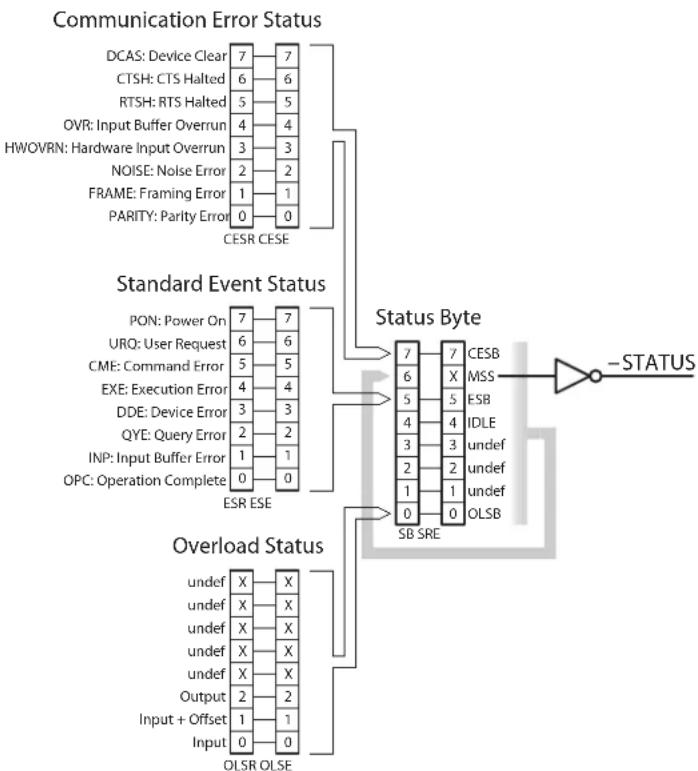
3.5 Status Model
TheSIM983statusregistersfollowthehierarchicalIEEE-488.2for-statusregisters mat.AblockdiagramofthestatusregisterarrayisgiveninFigure3.1.
flowchart
graph TD
    A["Communication Error Status"] --> B["DCAS: Device Clear 7"]
    A --> C["CTSH: CTS Halted 6"]
    A --> D["RTSH: RTS Halted 5"]
    A --> E["OVR: Input Buffer Overrun 4"]
    A --> F["HWOVRN: Hardware Input Overrun 3"]
    A --> G["NOISE: Noise Error 2"]
    A --> H["FRAME: Framing Error 1"]
    A --> I["PARITY: Parity Error 0"]
    A --> J["CESR CESE"]
    K["Standard Event Status"] --> L["PON: Power On 7"]
    K --> M["URQ: User Request 6"]
    K --> N["CME: Command Error 5"]
    K --> O["EXE: Execution Error 4"]
    K --> P["DDE: Device Error 3"]
    K --> Q["QYE: Query Error 2"]
    K --> R["INP: Input Buffer Error 1"]
    K --> S["OPC: Operation Complete 0"]
    K --> T["ESR ESE"]
    U["Overload Status"] --> V["undef X"]
    U --> W["undef X"]
    U --> X["undef X"]
    U --> Y["undef X"]
    U --> Z["undef X"]
    U --> AA["Output 2"]
    U --> AB["Input + Offset 1"]
    U --> AC["Input 0"]
    U --> AD["OLSR OLSE"]
    AE["Status Byte"] --> AF["7"]
    AE --> AG["X"]
    AE --> AH["X"]
    AE --> AI["X"]
    AE --> AJ["X"]
    AE --> AK["X"]
    AE --> AL["X"]
    AE --> AM["X"]
    AE --> AN["X"]
    AE --> AO["X"]
    AE --> AP["X"]
    AE --> AQ["X"]
    AE --> AR["X"]
    AE --> AS["X"]
    AE --> AT["X"]
    AE --> AU["X"]
    AE --> AV["X"]
    AE --> AW["X"]
    AE --> AX["X"]
    AE --> AY["X"]
    AE --> AZ["X"]
    AE --> BA["X"]
    AE --> BB["X"]
    AE --> BC["X"]
    AE --> BD["X"]
    AE --> BE["X"]
    AE --> BF["X"]
    AE --> BG["X"]
    AE --> BH["X"]
    AE --> BI["X"]
    AE --> BJ["X"]
    AE --> BK["X"]
    AE --> BL["X"]
    AE --> BM["X"]
    AE --> BN["X"]
    AE --> BO["X"]
    AE --> BP["X"]
    AE --> BQ["X"]
    AE --> BR["X"]
    AE --> BS["X"]
    AE --> BT["X"]
    AE --> BU["X"]
    AE --> BV["X"]
    AE --> BW["X"]
    AE --> BX["X"]
    AE --> BY["X"]
    AE --> BZ["X"]
Figure3.1: StatusregistermodelfortheSIM983ScalingAmplifier.
TherearetwocategoriesofregistersintheSIM983statusmodel:
EventRegisters: Theseread-only registers record the occurrence of defined events. If the event occurs, the corresponding bit is set to 1. Upon querying an event register, allset bits within it are cleared. These are sometimes known as "sticky bits," since once set, a bit can only be cleared by reading its value. Event registernamesend with SR.
Enable Registers: These read/write registers define a bitwise mask for their corresponding event register. If a bit position is set in an event register while the same bit position is also set in the enable register, then the corresponding summary bit message is set. EnableregisternamesendwithSE.
Atpower-on, all status registers are cleared.
IDLE:Indicates that the input buffer is empty and the command parser is idle. Can be used to help synchronize SIM983 query responses.
ESB:EventStatusBit.Indicateswhetheroneormoreoftheenabled eventsintheStandardEventStatusRegisteristrue.
MSS:MasterSummaryStatus.Indicateswhetheroneormoreofthe enabledstatusmessagesintheStatusByteregisteristrue.
CESB:CommunicationErrorSummaryBit.IndicateswhetheroneormoreoftheenabledflagsintheCommunicationErrorStatusRegisterhasbecometrue.
3.5.2 Service Request Enable (SRE)
EachbitintheSREcorrespondsone-to-onewithabitintheSBregister,andactsasabitwiseANDoftheSBflagstogenerateMSS.Bit6of theSREisundefined—settingithasnoeffect,andreadingitalways returns0.Thisregisterissetandqueriedwiththe*SRE(?) command.
Atpower-on, thisregisteriscleared.
3.5.3 Standard Event Status (ESR)
TheStandardEventStatusRegisterconsistsof8eventflags. These event flags are all "sticky bits" that are set by the corresponding events, and cleared only by reading or with the *CLS command. Reading a single bit (with the *ESR? i query) clears only Bit i.
WeightBitFlag
| 10 | OPC |
| 21 | INP |
| 42 | QYE |
| 83 | DDE |
| 164 | EXE |
| 325 | CME |
| 646 | URQ |
| 1287 | PON |
OPC:OperationComplete.Setbythe*OPC command.
INP:Inputbuffererror.Indicatesdatahasbeendiscardedfromthe inputbuffer.
QYE:QueryError.Indicatesdataintheoutputqueuehasbeenlost.
DDE:Device-DependentError.Indicates a failed autocalibration.
EXE:ExecutionError.Indicate the error in a command that was successfully parsed. Out-of-range parameters are an example.
CME:CommandError.Indicatesacommandparser-detectederror.
URQ:UserRequest.Indicatestatafront-panelbuttonwaspressed.
PON:PowerOn.Indicatesthatanoff-to-ontransitionhasoccurred.
3.5.4 Standard Event Status Enable (ESE)
TheESEactsasabitwiseANDwiththeESRregistertoproducethe single-bitESBmessageintheStatusByteRegister(SB).Theregister canbesetandqueriedwiththe*ESE(?) command.
Atpower-on, thisregisteriscleared.
3.5.5 Communication Error Status (CESR)
TheCommunicationErrorStatusRegisterconsistsof8eventflags; eachoftheflagsissetbythecorrespondingevent,andclearedonly byreadingtheregisterorwiththe*CLS command.Readingasing single bit (with the CESR? i query) clears only Bit i.
| WeightBitFlag |
| 10PARITY |
| 21FRAME |
| 42NOISE |
| 83HWOVRN |
| 164OVR |
| 325RTSH |
| 646CTSH |
| 1287DCAS |
PARITY:Parityerror.Setbyserialparitymismatchontheincomingdata byte.
FRAME:Framingerror.Setwhenanincomingserialdatabyteismissing theSTOPbit.
NOISE:Noiseerror.Setwhenanincomingserialdatabytedoesnot presentasteadylogiclevelduringeachasynchronousbit-periodwindow.
HWOVRN:HardwareOverrun.Setwhenanincomingserialdatabyteis lostduetointernalprocessorlatency.Causestheinputbuffer tobeflushed,andresetsthecommandparser.
OVR:InputbufferOverrun.Setwhentheinputbufferisoverrunby theincomingdata.Causestheinputbuffertobeflushed,and resetsthecommandparser.
RTSH:RTSHoldoffEvent.UnusedintheSIM983.
CTSH:CTSHoldoffEvent.UnusedintheSIM983.
DCAS:DeviceClear. Indicate that the SIM983 received the Device Clear signal (an RS-232
3.5.6 Communication Error Status Enable (CESE)
TheCESEactsasabitwiseANDwiththeCESRregistertoproduce the single-bit CESB message in the Status Byte Register (SB). The registercanbesetandqueriedwiththeCESE(?) command.
Atpower-on, thisregisteriscleared.
3.5.7 Overload Status (OLSR)
TheOverloadStatusRegisterconsistsof3eventflags; eachofthe flags is set by the corresponding overload, and cleared only by readingtheregisterorwiththe*CLS command. Readingasinglebit (with the OLSR? i query) clears only Bit i.
| Weight | Bit | Flag |
| 1 | 0 | Input |
| 2 | 1 | Input + Offset |
| 4 | 2 | Output |
| 8 | 3 | undef (0) |
| 16 | 4 | undef (0) |
| 32 | 5 | undef (0) |
| 64 | 6 | undef (0) |
| 128 | 7 | undef (0) |
Input: Inputoverload.Indicate that |V in| >10.0V(see also Section 1.2.4.1).
Input + Offset : Intermediate stage overload. Indicates that |V_in + V_ofs| > 10.0V .
Output: Outputoverload. Indicate that |V_out| >10.0V .
Reading this register (with the OLSR? query) clears all overload bits that a reset. If the overload condition persists, the bit will remain cleared until the overload condition ceases and re occurs. Use OVLD? to query the current state of the overload.
3.5.8 Overload Status Enable (OLSE)
TheOLSEactsasabitwiseANDwiththeOLSRegistertoproduce thesingle-bitOLSBmessageintheStatusByteRegister(SB).The registercanbesetandqueriedwiththeOLSE(?) command.
Atpower-on, thisregisteriscleared.
4 Performance Verification
This chapter describes the tests necessary to verify the SIM983 is operating correctly and with unspecified calibration.
In This Chapter
4.1 Verifying the DC Accuracy......4-2
4.1.1 Gettingready......4-2
4.1.2 Interpreting the accuracy specifications...4-2
4.1.3 Inputbiascurrent......4-4
4.2 VerifyingACPerformance......4-4
4.2.1 Transfercharacteristic......4-4
4.2.2Stepresponse....4-4
4.2.3Slewrate....4-6
4.2.4Totalharmonicdistortion......4-6
4.3NoiseCharacteristics......4-6
4.4PerformanceTestRecord .....4-8
4.4.1DCtest ....4-8
4.4.2Noisetest .....4-9
4.1 Verifying the DC Accuracy
ThegainandtheoffsetoftheSIM983ScalingAmplifierarecalibrated atthefactory.Besidesself-calibration,therearenouser-adjustable calibrationsettings.
4.1.1 Getting ready
ToverifytheDCperformanceoftheSIM983,oneneedsaDCsignal source(abletooutputeitherpolarity)and,asaminimum,avolt-meteraccurateto±500μVorbetter.Twovoltmeterswithmatched calibrationaremostconvenient,suchastwochannelsoftheStanford ResearchSystems'SIM970QuadDVM.TheSIM928IsolatedVoltage Sourceisrecommendedasthecalibrator;however,thewiperofa potentiometer connected to a power supply can be a simpler if less convenientsolution.TheDCsourcemustbequiet.Iftheverification isdonewithonlyonevoltmeter,cableshavetobeconnectedand disconnectedbetweenmeasurements,sothevoltagesourcemustbe stablewithinthevoltmeter'saccuracy.Nosuchstabilityisrequired iftwovoltmetersareused.
- WarmuptheSIM983foratleast2hours.
- If the voltmeter requires a warmup of a certain duration prior to establishing its accuracy specifications, or an autocalibration, becertaint o completethese.
- PerformanautocalibrationoftheSIM983asspecifiedinSection2.2.
Inordertoperformthemeasurements, connect the output of the voltagesourcetotheinput of the amplifier and to Voltmeter1. Connect the output of the SIM983 to Voltmeter2. If using only one voltage meter, use it to alternately measure the DC source voltage and the output voltage of the SIM983.
4.1.2 Interpreting the accuracy specifications
Gain and offset errors specified in the table on Page value contribute to the overall output error. The error in V_out = G × (V_in + V_ofs) is
$$ \delta V _ {\text { out }} = \delta G \times (V _ {\text { in }} + V _ {\text { ofs }}) + G \times \delta V _ {\text { ofs }}. $$
The gain error G and the offset error V_ofs both havetemperature-dependent contributions, mentioned in the specification table under “Stability”.
4.1.2.1 Error budget
Consider, for example, a measurement with G = +13.30 , V_in = 6.192V , and V_ofs = -5.480V , performed at a laboratory temperature of +28^ . The following are the worst-case contributions of the factor specified in the table on Pagevitothe output error:
SpecificationContributionToOverallError,V
| Gain accuracy, ±0.01Gainstability,(28°C- 23C)× (±10ppm/°C)=±50× 10-6Offset accuracy, ±1 mV ± 200 ppmOffsetstability,(28°C- 23C)× (±20μV/°C± 20ppm/°C)= ±100 μV ± 100 × 10-6 | ±0.01 × (6.192 - 5.480) = ±0.0071±50× 106 × (6.192 - 5.480) = ±0.000013.30 × (±0.001 ± 200 × 10-6 × (-5.480)) = ±0.027913.30 × (±0.0001 ± 100 × 10-6 × (-5.480)) = ±0.0086 |
| Total | =±0.0436 |
The output of the instrument is therefore
$$ V _ {\mathrm{out}} = 1 3. 3 0 \times (6. 1 9 2 \mathrm{V} - 5. 4 8 0 \mathrm{V}) \pm 0. 0 4 3 6 \mathrm{V} = (9. 4 7 \pm 0. 0 4) \mathrm{V} $$
iftheamplifierisperformingwithinitsspecifications.
Consider another example, with G = -0.19 , V_in = -3.954 V, and V_ofs = -5.480 V, performed at a laboratory temperature of +23 °C. For |G| < 1 , the specified offset error term is referenced to the output, according to Note4 on Page vii. The worst-case error budget is
SpecificationContributiontoOverallError,V
| Gain accuracy, | ±0.01 | ±0.01 × (-3.954 - 5.480) = ±0.0943 |
| Offset accuracy, | ±1 mV ± 200 ppm | ±0.001 ± 200 × 10-6× (-0.19) × (-3.954 - 5.480) = ±0.0014 |
| Total | =±0.0957 | |
Thestabilitytermsarezerobecausethetestistakenatthecalibration temperature. TheoutputoftheSIM983istherefore
$$ V _ {\text { out }} = - 0. 1 9 \times (- 3. 9 5 4 \mathrm{V} - 5. 4 8 0 \mathrm{V}) \pm 0. 0 9 5 7 \mathrm{V} = (1. 7 9 \pm 0. 1 0) \mathrm{V} $$
iftheunitisworkingaccordingtothespecifications.
When interpreting the result of a DC performance test of the SIM983, always account for the voltmeter accuracy specifications.
4.1.2.2 Recalibration
If the module fails its DC accuracy specifications, return it to Stanford ResearchSystemsforanewcalibration.
4.1.3 Input bias current
Asimpletestoftheinputcurrentcanbedonebyconnectingthe inputoftheSIM983totheinputofavoltmeterthathasamicrovolt range,suchastheSIM970.Thecurrentwillflowthroughaparallel combinationofthe1MΩinputresistanceoftheSIM983andtheinput resistanceofthevoltmeter,whichistypically10MΩintheSIM970 andisthatorgreaterinothervoltmeters.Dividethevoltmeter readingbytheresistance(e.g.0.9MΩ)toobtainthecurrent.Acurrent thatexceedsthespecificationinthetableonPageviindicatesa damagedfrontend.ThemoduleshouldthenbereturnedtoStanford ResearchSystemsforrepair.
4.2 Verifying AC Performance
MostinformationabouttheACbehavioroftheSIM983ScalingAmplifiercanbededucedbyobservingtheresponseoftheinstrument toasquarewaveattheinput.Theequipmentrequiredforthetestis afunctiongeneratorwithatmost25nssquare-waverisetime,such astheStanfordResearchSystems'DS345,andanoscilloscopewith atleast100MHzbandwidth. AnFFTspectrumanalyzer,suchas theStanfordResearchSystems'SR785,isneededtomeasuretotal harmonicdistortionandnoise.
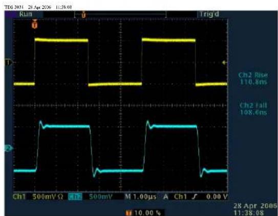
4.2.1 Transfer characteristic
Itispossibletomeasurethesmall-signalbandwidthoftheamplifier byapplyinga100mVpeak-peaksinewavetoitsinput,andincreasingthefrequencyoftheappliedsignaluntiltheoutputamplitude reducesto-3dB,i.e. 1 / 2 ,ofitslow-frequencyvalue.However,the small-signalbandwidthcanalsobemeasuredfromtherisetime oftheinstrument'sresponsetoasmall-inputstep.Forexample, inFigure4.1measuretherisetimeoftheoutputfrom 10% to 90% , i.e.-400mVto+400mV:
$$ t _ {\mathrm{rise}} = 1 1 1 \mathrm{ns}, $$
sothesmall-signalbandwidth
$$ f _ {- 3 \mathrm{dB}} (G = 1) = \frac {0 . 3 5}{t _ {\text { rise }}} = 3. 1 \mathrm{Mhz}, $$
which is consistent with the bandwidth expected from GBP=3.0MHzinthespecificationtableonPagevi.
4.2.2 Step response
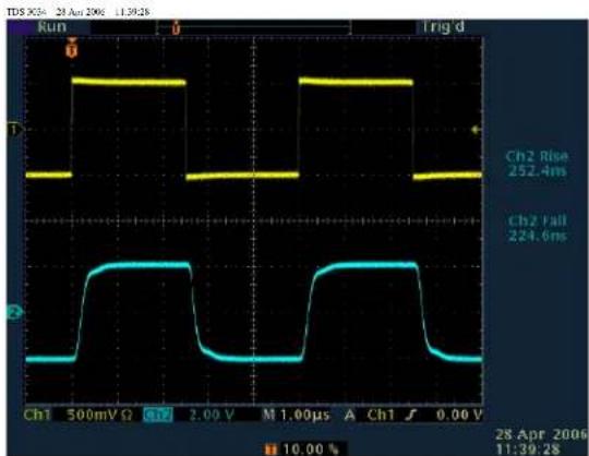
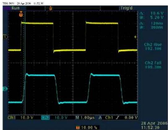
Figures4.1-4.6 illustrate the typical responses of SIM983 to steps in the input voltage. Figure 4.2 is for G = 4.00 , a value near the
top end of the range for BWTH = 1. According to the discussion in Section5.1.2.5, the amplifier is relatively overcompensated, resulting in an increased settling time. Compare with Figure 4.3, with G = 10.00 at the low end of the range for BWTH = 3. The amplifier is relatively undercompensated, and the smaller phase margin results in some overshoot and ringing.
line
| Time (ms) | Voltage (mV) | |-----------|--------------| | 0 | 500 | | 500 | 500 | | 1000 | 500 | | 1500 | 500 | | 2000 | 500 | | 2500 | 500 | | 3000 | 500 | | 3500 | 500 | | 4000 | 500 | | 4500 | 500 | | 5000 | 500 | | 5500 | 500 | | 6000 | 500 | | 6500 | 500 | | 7000 | 500 | | 7500 | 500 | | 8000 | 500 | | 8500 | 500 | | 9000 | 500 | | 9500 | 500 | | 10000 | 500 | | 10500 | 500 | | 11000 | 500 | | 11500 | 500 | | 12000 | 500 | | 12500 | 500 | | 13000 | 500 | | 13500 | 500 | | 14000 | 500 | | 14500 | 500 | | 15000 | 500 | | 15500 | 500 | | 16000 | 500 | | 16500 | 500 | | 17000 | 500 | | 17500 | 500 | | 18000 | 500 | | 18500 | 500 | | 19000 | 500 | | 19500 | 500 | | 20000 | 500 | | 26 Apr 26 | - | | - | - | | - | - | | - | - | | - | - | | - | - | | - | - | | - | - | | - | - | | - | - | | - | - | | - | - | | - | - | | - | - | | - | - | | - | ~118.8ms | | - | ~118.8ms | | - | ~118.8ms | | - | ~118.8ms | | - | ~118.8ms | | - | ~118.8ms | | - | ~118.8ms | | - | ~118.8ms | | - | ~117.8ms | | - | ~117.8ms | | - | ~117.8ms | | - | ~117.8ms | | - | ~117.8ms | | - | ~117.8ms | | - | ~117.8ms | | - | ~117.8ms | | - = - | ~- | | - = - | ~- | | - = - | ~- | | - = - | ~- | | - = - | ~- | | - = - | ~- | | - = - | ~- | | - = - | ~- | | - = - | ~- | | - = - | ~- |Figure4.1: ResponseoftheSIM983toa1.0V peak-peak step, G = +1.00 , V_ofs = 0.000V .
line
| Signal | Value | | ----------- | --------- | | Ch2 Rise | 252.4ms | | Ch2 Fall | 224.6ms |Figure4.2: ResponseoftheSIM983toa1.0V peak-peak step, G = +4.00, V_ofs =0.000V.

line
| Time (μs) | Run (mA) | Trig'd (ns) | |-----------|----------|-------------| | 0 | 0 | 176.4 | | 5 | 0 | 170.7 | | 10 | 0 | 176.4 | | 15 | 0 | 170.7 | | 20 | 0 | 176.4 | | 25 | 0 | 170.7 | | 30 | 0 | 176.4 | | 35 | 0 | 170.7 | | 40 | 0 | 176.4 | | 45 | 0 | 170.7 | | 50 | 0 | 176.4 | | 55 | 0 | 170.7 | | 60 | 0 | 176.4 | | 65 | 0 | 170.7 | | 70 | 0 | 176.4 | | 75 | 0 | 170.7 | | 80 | 0 | 176.4 | | 85 | 0 | 170.7 | | 90 | 0 | 176.4 | | 95 | 0 | 170.7 | | 100 | 0 | 176.4 | | 105 | 0 | 170.7 | | 110 | 0 | 176.4 | | 115 | 0 | 170.7 | | 120 | 0 | 176.4 | | 125 | 0 | 170.7 | | 130 | 0 | 176.4 | | 135 | 0 | 170.7 | | 140 | 0 | 176.4 | | 145 | 0 | 170.7 | | 150 | 0 | 176.4 | | 155 | 0 | 170.7 | | 160 | 0 | 176.4 | | 165 | 0 | 170.7 | | 170 | 0 | 176.4 | | 175 | 0 | 170.7 | | 180 | 0 | 176.4 | | 185 | 0 | 170.7 | | 190 | 0 | 176.4 | | 195 | 0 | 170.7 | | 200 | 0 | 176.4 | | 205 | 0 | 170.7 | | 210 | 0 | 176.4 | | 215 | 0 | 170.7 | | 220 | 0 | 176.4 | | 225 | 0 | 170.7 | | 230 | 0 | 176.4 | | 235 | 0 | 170.7 | | 240 | 0 | 176.4 | | 245 | 0 | 170.7 | | 250 | 0 | 176.4 | | 255 | 0 | 170.7 | | 260 | 0 | 176.4 | | 265 | 0 | 170.7 | | 270 | 0 | 176.4 | | 275 | 0 | 170.7 | | 280 | 0 | 176.4 | | | | | | | Ch1 | | | | | | | | | | | | | | | | | | | | | | | | | | | | | | | | | | | | | | | | | | | | | | | | | | | | | | | | | | | | | | | | | | | | | | | | | | | | | | | | | | | | | | | | | | | | | | | | | | | | | | | | | | | | | | | | | | | | | | | | | | | | | | | | | | | | | | | | | | | | | | | | | | | | | | | | | | | | | | | | | | | | | | | | | | | | | | | | | Ch1 | | | | | | | | | | | | | | | | | | | | | | | | | | | | | | | | | | | | | | | | | | | | | | | | | | | | | | | | | | | | | | | | Ch1 | | | | | | | | | | | | | | | | | | | | | | | | | | | | | | | | | | | | | | | | | | | | | | | | | | | | | | | | Ch1 | | | | | | | | | | | | | | | | | | | | | | | | | | | | | | | | | | | | | | | | | | | | | | | | Ch1 } , \ , \ , \ , \ , \ , \ , \ , \ , \ , \ , \ , \ , \ , \ , \ , \ , \ , \ , \ , \ , \ , \ , \ , \ , \ , \ .Figure4.3: Response of the SIM983 to a 1.0V peak-peak step, G = +10.00 , V_ofs = 0.000V .

line
| Time (s) | Ch2 Rise (ms) | Ch2 Fall (ms) | |----------|---------------|---------------| | 0 | 282.3 | 273.1 |Figure4.4: Response of the SIM983 to a 1.0V peak-peak step, G = +19.99 , V_ofs = 0.000V .
Theasymmetricalpositive-goingandnegative-goingresponses in Figures 4.5 and 4.6 are ultimate artifacts of the single-ended, as opposed to differential, topology of the input voltage buffer (Section5.1.2.1).
line
| Time (ns) | Amplitude (V) | |-----------|---------------| | 0 | 10.6 | | 300 | 5.20 | | 300 | 120 | | 300 | 300 | | 300 | 192.1 | | 300 | 198.3 |Figure4.5: ResponseoftheSIM983toa20V peak-peak step, G = +1.00, V_ofs =0.000V.
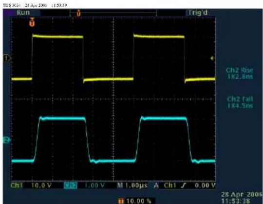
Figure4.6: Response of the SIM983 to a 20V peak-peak step, G = +0.10 , V_ofs = 0.000V .
4.2.3 Slew rate
Slewrateinformationiscontainedwithinthelarge-input,large-outputstepresponse(Figure4.5). ^2 Afteraninitialdelay,theoutput rises from -5.4 V to +5.2 V in 120 ns. The slew rate
$$ \mathrm{SR} = \frac {5 . 2 - (- 5 . 4)}{1 2 0 \times 1 0 ^ {9}} = 8 8 \mathrm{V} / \mu \mathrm{s}. $$
4.2.4 Total harmonic distortion
Figure4.7 showsadistortionmeasurementmadeontheSR785 FFTSpectrumAnalyzer.
4.3 Noise Characteristics
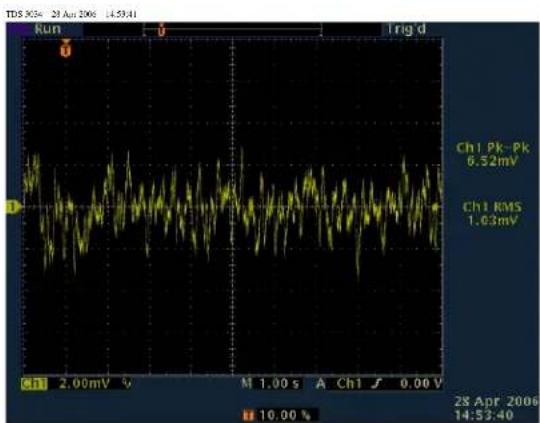
Figure4.8 shows noise plot of the SIM983 up to f = 100kHz , measured with an SR785. Not the quite weak dependence of the input-referenced noise on the gain for |G| ≥ 1 . Figure 4.9 shows the time dependence of the output voltage of the SIM983. The 0.17Hz single-pole high-pass, and 10Hz eighth-order low-pass filtering was provided by the SIM965 Analog Filter.

line
| Frequency (Hz) | Voltage Response (V rms) | | -------------- | ------------------------ | | 0 | 10^-6 | | 2000 | 10^0 | | 4000 | 10^-3 | | 6000 | 10^-5 | | 8000 | 10^-5 | | 10000 | 10^-5 | | 12000 | 10^-5 |Figure4.7: Responsespectrum of theSIM983atG=+1.00toa1.0kHz, 1.0Vrmssinewave, showingharmonic artifactsat<1× 10 ^-5 oftheprincipal. The total THD for 10 harmonics is -96dB, as measured by an SR785. The THD does not degrade with highergain, or larger input signal, up to the overload limits of theSIM983.

line
| Frequency (Hz) | Voltage Noise (nV/√Hz) for G = +1, 00 | Voltage Noise (nV/√Hz) for G = +19, 99, 87 | Voltage Noise (nV/√Hz) for G = +0, 13 = 70 | | -------------- | ------------------------------------- | ------------------------------------------ | ----------------------------------------- | | 1 | ~1000 | ~800 | ~600 | | 10 | ~200 | ~150 | ~100 | | 100 | ~50 | ~40 | ~30 | | 1000 | ~30 | ~25 | ~20 | | 10000 | ~25 | ~20 | ~15 | | 100000 | ~25 | ~20 | ~15 |Figure 4.8: Noise of the SIM983, referenced to the input for |G| ≥ 1 .
line
| Time (s) | Voltage (mV) | |----------|--------------| | 2.00 | 6.52 | | 0.00 | 1.03 |Figure 4.9: 0.1 Hz to 10 Hz noise of the SIM983, G = +19.99, additional gain of 50.
4.4 Performance Test Record
4.4.1 DC test
Serialnumber
Labtemperature(°C)=
| G | V_in (V)(V) | V_ofs (V) | V_out (V) | G × _in + V_ofs (V) | Error(V) | Gain accuracy error (V) | Gain stability error (V) | Offset accuracy error (V) | Offset stability error (V) | Cal within spec? |
| 12 | ||||||||||
4.4.2 Noise test
Serialnumber
Inputbiascurrent(pA)=
Noisevolage, nV/ √Hz:
| G = -0.10 | G = +0.10 | G = -1.00 | G = +1.00 | G = -19.99 | G = +19.99 | |
| f=1kHz | ||||||
| f=10kHz |
5 Circuit Description
ThischapterpresentsabriefdescriptionoftheSIM983circuitdesign. Acompletepartslistandcircuitschematicsareincluded.
In This Chapter
5.1 CircuitDiscussion....5-2
5.1.1 Microcontrollerinterface......5-2
5.1.2Theamplifier....5-2
5.1.3Frontpanel....5-6
5.2PartsList....5-6
5.3SchematicDiagrams....5-10
5.1 Circuit Discussion
The following sections correspond to schematic pages at the end of the manual.
5.1.1 Microcontroller interface
TheSIM983iscontrolledbymicrocontrollerU107.
5.1.1.1 Digital control and clock stopping
Acriticalaspectofthedesignistheclock-stopcircuitryimplemented byU102andU105.AsimpleRCoscillatorisenabledordisabledat Pin1ofU105.Thispinisdrivenbysynchronizingflip-flopU102Bto ensurethatno"runt"clockpulsesareproducedthatwouldviolate theminimunclockperiodofU107.Fourseparateclockstarting signalsarecombinedbyU103andU104,asdiscussedinSection2.4.
ThefaststarttimeoftheRCoscillatorensuresthatincomingserialdatawillbecorrectly decodedbythemicrocontroller'sUART, evenwhentheclockisstartedbytheserialstartbitoftheincoming data.Whenthemicrocontrollerhascompletedallpendingactivity, itdrivestheSTOPsignalHIGH(Pin71ofU107), effectivelyhalting its own processor clock. In this way, the SIM983 guarantees that no digitalclockartifactscanbegeneratedduringquiescentoperation.
5.1.1.2 Power and grounds
Aseparateclean+5 VsourceisprovidedbyvoltageregulatorU109 topowertheanalogcircuitryoftheamplifier. Eachpointinthe circuitthatconnectstoGround2(Section2.1.2)isseparatelyrouted toPin8ofinterfaceconnectorJ101,formingastargroundonLayer3 ofthecircuitboard.
5.1.2 The amplifier
The signal path in the SIM983 Scaling Amplifier consists of five stages: the high-impedance input voltage buffer, the summing amplifier, the voltage inverter, the programmable gain stage, and the passive LRC filter. Other part of the amplifier circuit are the precision voltage reference, the offset voltage generator, and the output microvoltmeter, used for autocalibration.
5.1.2.1 Input voltage buffer
The input buffer is a high-impedance (40pA max bias current), high-slew-rate (1200 V/ s typ.), high-speed (105 MHz typ. small-signal
bandwidth)compositeoperationalamplifier,runningatgain1.Cas-codedradiofrequencyFETQ201providestheslewrateandthebandwidth,whereasU201,aprecisionJFEToperationalamplifier(op-amp),disciplinesQ201toamaximumof900μVofoffsetvoltage, 12μV/°Cmaximumoffsetdrift,and8.5nV/√Hztypicalnoise. ^1 The outputofthevoltagebufferismonitoredforoverloadbycomparatorU213,whichtripsatthevoltagelimitsspecifiedinSection1.2.4.1.
5.1.2.2 Offset voltage generator
TheoffsetvoltageisprovidedbyU204,a16-bitdigital-to-analogconverter(DAC).BecauseoftheultralowdriftoftheDACandprecision resistornetworkR215,thetemperaturestabilityofthegenerated offsetislargelydeterminedbythe5ppm/ °Ctypicalperformance of scaling resistor R217. The integral nonlinearity of U204 puts a200ppmlimitontheoverallaccuracyoftheinstrument'soffset. Asecond,12-bitDACU206allowsforfinetuningofthegenerated offset,cancellingthecontributionoftheinputoffsetvoltageofU201 andoffsetsinsubsequentstagesinordertoachievethespecifiedaccuracy. The offset voltage is filtered by the 6.3 kΩ output resistance ofU204incombinationwithC206,withf -3dB =11Hz.
5.1.2.3 Summing amplifier
The voltagesattheoutputsoftheinputbufferandthetwooffset-generating DACs are combined by a summing amplifier built aroundU208A. Thislow-noise, high-speedop-ampisdisciplined byonehalfofprecisionop-ampU207, soitsinputoffsetcontributes negligibly to the overall offset error and the offset drift. However, the inputbiascurrentoftheop-ampdoescontributetotheerror, and thiscontributionispartiallycancelledbyaconstantcurrentinjected intothesummingnodethroughR219. Theremainingcontribution iscalibratedoutviaU204andU206.
At this stage, three major contributions to the overall noise of theSIM983comeintoplay;thesecontributionsarecomparablein magnitude,andaddinquadrature.The1.5nV/ noise(at10kHz) ofU208facesanoisegainof6fromR216andR217. Theinput buffercontributesanother9.5nV/ . Finally,theJohnsonnoise ofthe2.5kΩresistorsofR216andthe604ΩR217,timesthenoise gain,yields16.5nV/ ,referencedtotheinput. Therefore,the totalnoiseattheoutputofthisstageistypically21nV/ . The inputbiascurrentofU208,passingthroughthefeedbackportion
ofR216,onlygeneratesacontributionof3nV/whenaddedinquadrature.
,insignificant
ScalingresistornetworkR216ishighlystable, and does not contribute appreciably to the drift of the regain.
5.1.2.4 Voltage inverter
Theinverson, ifrequired, is performed by the other half of dual op-ampU208. Precision resistornetwork R222 is connected in such a way that thenoise gain of the op-ampis always 2, ensuring stability from oscillation. The Johnson noise of thenetwork contributes the overall noise of the SIM983, resulting in 22nV/ (typ., at 10kHz) atthestage's output.
Because the inverting stage is not disciplined, its offset contributes to the overall error; this offset typically drifts by 10 V/^ , and, combined with the drift of the input voltage buffer, this error determines the offset stability of the instrument. The error produced by the input bias current of the op-ampiscalibrated out.
The output of the summing amplifier is monitored for overload by comparator U214, triggered at the voltage limits discussed in Section1.2.4.1.
5.1.2.5 Gain stage
The variable-gainelement is one half of high-speedop-ampU211, connected in the inverting configuration. Two matched converters of dual multiplying DAC(MDAC)U210 serve as variable input and feedback resistors for this inverting amplifier:
$$ | G | \quad \frac {R (\mathrm{U} 2 1 0 \mathrm{B})}{\overline {{R}} (\mathrm{U} 2 1 0 \mathrm{A})}. $$
When |G| ≤ 1 , U210B is set to or near its minimum resistance value of 10k , and U210A, to an equal or greater resistance. Thesituation is reversed for |G| > 1 . The 12-bit resolution of the MDACs places limitations on the values of achievable gains. ThetwoMDACstrackto within 10ppm / ^ , and thistermisthedominant one for the stability of the instrument's gain.
Similarly to the summing portion of U208, the gain amplifier (U211A) is disciplined by U207 Binorderto achieve an negligible contribution to the overall offset, offset drift, and noise. However, the error from the input bias current of U211A (which is multiplied by the resistance R (U210B)) is not negligible. ^2 A first-order cancellation of the
biasisachieved by mirroring the input current of these second half, U211B, and injecting it into the input node of U211A. Theremaining input current produces a drift term that is roughly the same as, or smaller than, the other dominant contribution to the offset stability of the instrument.
This cancellationschemeincreases thecontribution of the gain stagetothe overall noise. Thenoise current of U211 is multiplied by R(U210B) and by 2 . As R(U210B) increases linearly with the gain for |G| ≥ 1 , this terms yields 21 nV/ , referenced to the input.
The remaining noise contribution is from R(U210A) and R(U210B) . Their Johnsonnoise at the output of the staged dependence on the gain as
$$ e _ {n} \propto \sqrt {| G | (1 + | G |)}, $$
andforlargegainsisjustthenoiseofthe10kΩresistorR(U210A), referencedtotheinput.This13.5nV/ √Hztermaddsinquadrature withthe22nV/ √Hzcontributionoftheearlierthreestages,andwith thebias-currentcontribution,toyield34nV/ √Hz(f≥10kHz).At most frequencies f ≥ 100 Hz, and for |G| ≥ 1, the input-referenced noiseoftheSIM983isindependentofthegaintowithin2nV/ √Hz.
The capacitances of the analog switches ^3 that configure the variable-resistance MDAC add together at the output of the MDAC. This capacitance becomes the input capacitance of the inverting amplifier, and its value places the ultimate limit on the small signal bandwidth achievable in the gain stage and with it, in the whole instrument. The capacitancetogether with R(U210A) forms an input pole, so if the gain of the amplifier is not rolled off with a capacitor in the feedback path, the amplifier will oscillate. The amount of compensation feedback capacitanced desired for stability from oscillation increases with decreasing |G|. The compensation network consists of PFETs Q205–Q208, functioning as switches and chosen for ultralow OFF capacitance, and capacitors C208–C210. One, both, or none of C209 and C210 are inserted into the feedback path for four ranges of the gain, resulting in four possible values of the gain-bandwidth product of the stage (Pagevi). With the feedback capacitor selected, the phase margin of the amplifier improves with increasing |G|, and with the overshoot and ringing in the step response decrease.
Output voltage buffer U212 enables the instrument to drive 50 Ω loads. Comparator U215 indicates an overload at the specified output voltagelimits(Section1.2.4.2).
5.1.2.6 Output filter
The performance of the passive filter, composed of L201, R226, R227, and C211, is described on Schematic Page 2. The filter eliminates the broad-spectrum noise of high-band width amplifiers Q201, U208, and U211 beyond a few megahertz, while adding an negligible amount of overshoot in the step response.
5.1.2.7 Output microvoltmeter
The analog-to-digital converter(ADC) used for autocalibration is a part of microcontroller U107. The output signal is amplified by precision op-amp U217, then shifted by +2.5V by shunt reference D201 and fed into the ADC.
5.1.3 Front panel
Brightred7-segmentLEDdisplaysU302,U304,U306,U307,U309,U311,U313,andU314,andoverloadLEDsD301andD302aredriven byshiftregistersU301,U303,U305,U308,U310,U312,andU315.
5.2 Parts List
| STANFORD RESEARCH SYSTEMS, INC. | ||||||
| SIM983 Scaling Amplifier Circuit Board (1 of 1) Revision D | ||||||
| BILL OF MATERIALS | May 5, 2006 | |||||
| Item | Qty. | Reference | Part | SRS P/N | Manufacturer | Manf. P/N |
| 1 | 2 | C101,C102 | 22μ T | 5-00327-030 | VISHAY | 199D226X9035E6B1 |
| 2 | 10 | C103,C110,C111,C205,C221,C222,C223,C224,C225,C226 | 10μ T | 5-00098-030 | VISHAY | 199D106X9035D2B1 |
| 3 | 1 | C104 | 330p | 5-00381-100 | KEMET | C1206C331J5GACTM |
| 4 | 1 | C105 | 9.0--50p | 5-00106-090 | XICON | 24AA024 |
| 5 | 3 | C106,C107,C108 | 1000p | 5-00387-100 | KEMET | C1206C102J1GACTM |
| 6 | 5 | C109,C217,C218,C219,C220 | 1.0μ T | 5-00099-030 | VISHAY | 199D105X9035A2B1 |
| 7 | 1 | C201 | 2.7p NP0 ±0.25p | 5-00630-100 | KEMET | C1206C279C5GACTM |
| 8 | 2 | C202,C210 | 3.3p NP0 ±0.25p | 5-00357-100 | KEMET | C1206C339C5GACTM |
| 9 | 3 | C203,C204,C209 | 1.5p NP0 ±0.25p | 5-00353-100 | KEMET | C1206C159C5GACTM |
| 10 | 2 | C206,C216 | 2.2μ MPE 5% | 5-00584-050 | PANASONIC | ECQ-E1225JFB |
| 11 | 2 | C207,C213 | 4.7μ MPE 5% | 5-00073-050 | XICON | 146-250V4.7K |
| 12 | 1 | C208 | 0.5p NP0 ±0.25p | 5-00592-100 | AVX | 12065A0R5C |
| 13 | 1 | C211 | 1500p NP0 5% | 5-00389-100 | KEMET | C1206C152J5GACTM |
| 14 | 2 | C212,C214 | 1.0μ MPE 5% | 5-00245-050 | WIMA | MKS4/1/63/5RM10 |
| 15 | 1 | C215 | 10μ MPE 10% | 5-00072-050 | PANASONIC | ECQ-E1106KF |
5.2PartsList5-7
| Item | Qty. | Reference Part SRS P/N Manufacturer Manf. P/N | ||||
| 16 43 | X101 | ,X102,X103,X104,X105, 0.1μ 5-00 | 299-100 KEMET C1206C104 | K5RACTM | ||
| X106,X107,X108,X109,X110, | ||||||
| X111,X112,X113,X114,X115, | ||||||
| X201,X202,X203,X204,X205, | ||||||
| X206,X207,X208,X209,X210, | ||||||
| X211,X212,X213,X214,X215, | ||||||
| X216,X217,X218,X219,X220, | ||||||
| X221,X301,X302,X303,X304, | ||||||
| X305,X306,X307 | ||||||
| 17 | 2 | D101,D102 | BAT54S | 3-00945-143 | DIODES INC | BAT54S-7 |
| 18 | 1 | D201 | TL431CDBV | 3-01133-123 | PHILIPS | TL431CD5 |
| 19 | 1 | D202 | BAV99 | 3-00896-145 | ON SEMI | BAV99LT1 |
| 20 2 | D301 | D302 Red 3-00425-060 LITEON | LTL-709E | |||
| 21 | 1 | J101 | 15 Pin D | 1-00367-040 | CINCH | DAKL-15PATI-E |
| 22 0 | J102 | Header 0.100" 4×1 no part | ||||
| 23 | 1 | J103 | Socket 0.100" 3×2 | 1-00302-010 | SAMTEC | CES-103-01-G-D |
| 24 | 1 | J104 | Header 0.050" 7×2/Mixed | 1-01063-109 | SAMTEC | FTSH-107-04-L-M-T |
| 25 0 | J201 | J202,J203 Flying | Leads no part | |||
| 26 | 1 | J301 | Socket 0.050" 7×2/SM | 1-01064-119 | SAMTEC | FLE-107-01-G-DV-A |
| 27 | 3 | L101,L102,L103 | FR43 bead | 6-00174-051 | FAIR-RITE | 2643666611 |
| 28 | 1 | L201 | 1.2μ 5% 500mA | 6-00676-100 | API DELEVAN | 1210-122J |
| 29 0 | MH101 | MH102,MH103,MH104 Mouning Hole no part | ||||
| 30 | 2 | Q201,Q202,Q203 | MMBF4416 | 3-01324-152 | VISHAY | SST4416 |
| 31 | 1 | Q204 | MMBT2907A | 3-00927-150 | ON SEMI | MMBT2907ALT1 |
| 32 | 4 | Q205,Q206,Q207,Q208 | MMBF5460 | 3-01305-152 | FSC | MMBF5460 |
| 33 | 5 | R101,R111,R112,R115,R117 | 100k 5% | 4-01527-100 | VENKEL | CR1206-8W-104JT |
| 34 | 1 | R102 | 1.0k | 4-01479-100 | VENKEL | CR1206-8W-102JT |
| 35 | 1 | R103 | 210 | 4-01052-110 | VENKEL | TRN55CF-2100TR |
| 36 | 1 | R104 | 3.9k | 4-01493-100 | VENKEL | CR1206-8W-392JT |
| 37 | 1 | R105 | 3.9k×4 D | 4-00917-120 | BI | BCN164A-392-J7 |
| 38 | 3 | R106,R261,R314 | 4.7k | 4-01495-100 | VENKEL | CR1206-8W-472JT |
| 39 | 1 | R107 | 22k | 4-01511-100 | VENKEL | CR1206-8W-223JT |
| 40 | 1 | R108 | 10 | 4-01431-100 | VENKEL | CR1206-8W-100JT |
| 41 | 3 | R109,R118,R119 | 270 | 4-01465-100 | VENKEL | CR1206-8W-271JT |
| 42 | 5 | R110,R120,R121,R227,R262 | 100 5% | 4-01455-100 | VENKEL | CR1206-8W-101JT |
| 43 | 3 | R113,R114,R260 | 10k | 4-01503-100 | VENKEL | CR1206-8W-103JT |
| 44 | 1 | R116 | 100k×4 D 5% | 4-01704-120 | CTS | 742C083104J |
| 45 | 1 | R122 | 150 5% | 4-01459-110 | VISHAY | CRCW1206151JRT1 |
| 46 | 1 | R123 | 121 | 4-01029-110 | VENKEL | TRN55CF-1210TR |
| 47 | 1 | R124 | 365 | 4-01075-110 | VENKEL | TRN55CF-3650TR |
5-8 CircuitDescription
| Item | Qty. | Reference Part SRS P/N Manufacturer | Manf. P/N | |||
| 48 8 | R201 | R219,R223,R224,R233, 1.00M 4-01405-110 VENKEL TRN55CF-1004TR | ||||
| R234,R242,R249 | ||||||
| 49 | 2 | R202,R203 | 1.00k 1.0W flameproof | 4-00542-000 | VISHAY | CPF11K0000FKB14 |
| 50 2 | R204 | R205 200 1% | 4-01050-110 VENKEL TRN55CF-2000TR | |||
| 51 | 1 | R206 | 510 | 4-01472-100 | VENKEL | CR1206-8W-511JT |
| 52 | 8 | R207,R210,R211,R212,R239, R246,R253,R258 | 1.00k | 4-01117-110 | VENKEL | TRN55CF-1001TR |
| R208 | 280 | 4-01064-110 | VENKEL | TRN55CF-2800TR | ||
| 53 | 1 | R209 | 4.02k | 4-01175-110 VENKEL TRN55CF-4021TR | ||
| 54 1 | R209 | 4.02k | 4-01175-110 VENKEL TRN55CF-4021TR | |||
| 55 | 1 | R213 | 909 | 4-01113-110 | VENKEL | TRN55CF-9090TR |
| 56 1 | R214 | 14.0k | 4-01227-110 VENKEL TRN55CF-1402TR | |||
| 57 2 | R215 | R222 1.000k×2 1ppm/K 0.1%rat 4-01738-122 VISHAY MPM2001AT | ||||
| 58 1 | R216 | 2.500k×2 1ppm/K 0.1%rat 4-01721-122 VISHAY MPM5001AW | ||||
| 59 | 1 | R217 | 604.0 5ppm/K | 4-01733-000 | VISHAY | PTF56604R00BZBF |
| 60 | 1 | R218 | 523k | 4-01378-110 | VENKEL | TRN55CF-5233TR |
| 61 1 | R220 | 49.9k | 4-01230-110 VENKEL TRN55CF-4992TR | |||
| 62 | 1 | R221 | 10.0 | 4-00925-110 | VENKEL | TRN55CF-10R0TR |
| 63 1 | R225 | 10.0k | 4-01213-110 VENKEL TRN55CF-1002TR | |||
| 64 1 | R226 | 2.00k | 4-01146-110 VENKEL TRN55CF-2001TR | |||
| 65 | 1 | R228 | 35.7 2W flameproof | 4-01735-000 | VISHAY | CPF235R700FKB14 |
| 66 1 | R229 | 5.1 | 4-01424-100 VENKEL CR1206-8W-5R1JT | |||
| 67 | 2 | R230,R231 | 13.3 2W flameproof | 4-01736-000 | VISHAY | CPF213R300FKB14 |
| 68 3 | R232 | R241,R248 365k | 4-01363-110 VENKEL TRN55CF-3653TR | |||
| 69 | 1 | R235 | 649k | 4-01387-110 | VENKEL | TRN55CF-6493TR |
| 70 3 | R236 | R243,R250 221k | 4-01342-110 VENKEL TRN55CF-2213TR | |||
| 71 | 6 | R237,R238,R244,R245,R251, R252 | 2.4M | 4-01560-100 | VISHAY | CRCW1206245JRT1 |
| R240,R247,R254 | 3.01k | 4-01163-110 | VENKEL | TRN55CF-3011TR | ||
| 72 | 3 | R255 | 392 | 4-01078-110 | VENKEL | TRN55CF-3920TR |
| 73 | 1 | R256 | 732 | 4-01104-110 | VENKEL | TRN55CF-7320TR |
| 74 | 1 | R257 | 249 | 4-01059-110 | VENKEL | TRN55CF-2490TR |
| 75 | 1 | R259 | 150k 1% | 4-01326-110 | VENKEL | TRN55CF-1503TR |
| 76 | 13 | R301,R302,R303,R304,R305, R306,R307,R308,R309,R310, R311,R312,R313 | 4.7k×4 D | 4-00911-120 | BI | BCN164A-472-J7 |
| 77 | 13 | R301,R302,R303,R304,R305, R306,R307,R308,R309,R310, R311,R312,R313 | ||||
| 78 2 | R315 | R316 2.2k | 4-01487-100 VENKEL CR1206-8W-222JT | |||
| 79 | 5 | S301,S302,S303,S304,S305 | B3F-1052 | 2-00053-000 | OMRON | B3F-1052 |
| 80 0 | TP101 | Test Point no part | ||||
5.2PartsList5-9
| Item | Qty. | Reference Part SRS P/N Manufacturer | Manf. P/N | |||
| 81 2 | U101 | U108 74HC14 3-00662-103 PHILIPS 74HC14D | ||||
| 82 1 | U102 | 74HC74 3-00742-103 TI SN74HC74D | ||||
| 83 2 | U103 | U104 74HC21 3-01502-103 PHILIPS 74HC21D | ||||
| 84 1 | U105 | 74AC00 | 3-01405-100 FSC | 74AC00SC | ||
| 85 1 | U106 | MAX6348 4.4V | 3-00903-124 MAXIM | MAX6348UR44-T | ||
| 86 1 | U107 | 68HC912B32 | 3-01379-114 FREESCALE | MC68HC912B32CFU8 | ||
| 87 1 | U109 | LM317L | 3-00096-030 ON SEMI | LM317LZ | ||
| 88 1 | U201 | AD8510A | 3-01318-120 ANALOG | AD8510AR | ||
| 89 2 | U202 | U203 LM7121 | 3-01306-120 NSC | LM7121IM | ||
| 90 1 | U204 | MAX5541C | 3-01217-171 MAXIM | MAX5541CSA | ||
| 91 2 | U205 | U207 OPA2227A | 3-01471-120 TI OPA2227UA | |||
| 92 1 | U206 | LTC1452C | 3-00652-171 LTC | LTC1452CS8 | ||
| 93 1 | U208 | THS4032 | 3-01219-120 TI THS4032CDGN | |||
| 94 1 | U209 | DG419 | 3-01367-122 VISHAY | DG419DY | ||
| 95 1 | U210 | AD5415 | 3-01171-171 ANALOG | AD5415YRU | ||
| 96 1 | U211 | EL2244 | 3-01300-120 INTERSIL | EL2244CS | ||
| 97 1 | U212 | BUF634P | 3-01221-120 TI BUF634P | |||
| 98 3 | U213 | U214,U215 | LM393 | 3-00728-121 TI LM393D | ||
| 99 1 | U216 | MAX6225BC | 3-00970-123 MAXIM | MAX6225BCSA | ||
| 100 | 1 U217 | OPA277A | 3-01370-120 TI OPA277UA | |||
| 101 | 7 | U301,U303,U305,U308,U310, | 74HC595A | 3-00672-103 | ON SEMI | MC74HC595ADT |
| U312,U315 | ||||||
| 102 | 2 | U302,U309 | HDSP-A107 | 3-01424-061 | AVAGO | HDSP-A107 |
| 103 | 6 | U304,U306,U307,U311,U313, | HDSP-A101 | 3-00290-061 | AVAGO | HDSP-A101 |
| U314 | ||||||
| 104 | 5 | no designator | Button Cap | 0-00996-999 | OMRON | B32-1000 |
| 105 | 4 | no designator | 4-40x1/4 Pan Phil | 0-00187-999 | ACF | PPM-04C04-0-Z |
| 106 | 4 | no designator | #4 Split Washer | 0-00096-999 | J&M | 4NLOCLZ |
| 107 | 2 | no designator | 4-40x3/8 Flat Phil | 0-00835-999 | ACF | PUM-04C06-0-Z |
| 108 | 4 | no designator | 4-40x1/8 Pan Slot | 0-00148-999 | ACF | SPM-04C02-0-Z |
| 109 | 4 | no designator | 4-40x1/8 Pan Phil | 0-00515-999 | ACF | PPM-04C02-0-Z |
| 110 | 8 | no designator | 4-40x1/8 Black Flat Phil | 0-00371-999 | ACF | PUM-04C03-0-B |
| 111 | 6 | no designator | 1.5" 24AWG Uninsulated | 0-00772-999 | > | > |
| 112 | 1 | no designator | 6.5" 22AWG White | 0-00436-999 | > | > |
| 113 | 1 | no designator | 6.5" 22AWG Black | 0-00268-999 | > | > |
| 114 | 1 | no designator | 7.5" 22AWG Red | 0-00154-999 | > | > |
| 115 | 1 | no designator | 7.5" 22AWG Black | 0-00161-999 | > | > |
| 116 | 1 | no designator | 3.0" 22AWG Red | 0-00006-999 | > | > |
| 117 | 2 | no designator | BNC Insulated | 1-00073-256 | AMPHENOL | 31-10-4052 |
| 118 | 1 | no designator | BNC | 1-00003-256 | TYCO | 227169-4 |
| 119 | 1 | no designator | Circuit Board | 7-01639-999 | FAB | SIM983 Circuit Board Rev. D |
| 120 | 1 | no designator | Front Panel | 7-01603-999 | FAB | SIM983 Front Panel Rev. B |
| 121 | 1 | no designator | Lexan Overlay | 7-01605-999 | FAB | SIM983 Front Lexan Rev. B |
| 122 | 1 | no designator | Rear Panel | 7-01604-999 | FAB | SIM983 Rear Panel Rev. A |
| 123 | 2 | no designator | Top/Bottom Bracket | 7-00933-999 | FAB | SIM Sglw. Bracket Rev. D |
| 124 | 2 | no designator | Module Cover | 7-00932-999 | FAB | SIM Module Cover Rev. C2 |
| 125 | 4 | no designator | Rubber Foot | 0-00188-999 | MOUSER | 5167-202 |
| 126 | 1 | no designator | Serial Number Label | 9-01545-999 | FAB | SIM SN Label Rev. A |
5.3 Schematic Diagrams
Circuitschematicdiagramsfollowthispage.
text_image
Electrical schematic diagram with labeled components, ICs, and wiring connections
text_image
Electrical schematic diagram with labeled components including transistors, capacitors, inductors, and control circuits.
text_image
Electrical schematic diagram of a 7-segment display driver circuit with labeled components and connectionsAppendix A Index
STATUSsignal,1-2,1-7,3-12,13,3-20
Accuracy,iii,4-2
gain,seeGain,accuracy
offset,seeOffset,accuracy
verifyingatDC,4-2,4-8
Autocalibration,vii,1-2,2-2,3,3-11,3-13,3-17,3-21,4-2,5-2,5-6
Bandwidth,vi,1-2,2-3,3-6,3-10,11,4-4,5,5-2,5-5
default,1–6,3–11,3–14
Baudrate,1–9,3–6
Biascurrent,vi,4-3,5-2
Blockdiagram,1-2
BNC,iii,vi,vii,2-2
Buffer
input,3-6,3-20-22
overflow,3–6,3–22
voltage,seeInput,voltagebuffer
output,seeOutputqueue
voltage,seeOutput,voltagebuffer
Button,3-11,3-13,3-21
[gain],1-3,2-3,3-13
[offset],1-4,3-13
[polarity],1-3,4,2-3,3-13
Calibration,seeFactorycalibration
Circuitschematics,seeSchematicdiagrams
Clockstopping,1-2,2-4,3-10,3-14,5-2
Command
error,3–16,3–21
parameters,3–7,3–16
separator,3–7
terminator,3–6,7,3–14,3–17
Compensation,2-3,4-4,5-5
Consolemode,3–6,3–14,15
DB-15,1-7,8,2-2
DB-9
female,1–8
male,1–8
Defaultconfiguration,seeReset
DeviceClear,3-6,3-15,3-17,3-22
Deviceerror,3–16,3–21
Dimensions, vii
Distortion,see Totalharmonicdistortion
DS345,4-4
Error
budget,4-2
command,seeCommand,error
Executionerror,3-15,3-21
Factorycalibration,4–2,3
Firmwareerevision,3–15
Flowcontrol,1–9,3–6,3–17
Frontpanel,1-2,3,2-3,4,3-11
operation,1–3
Fullduplex,seeConsolemode
Gain,iii,vi,1-2,3,1-6,2-2,3,3-6,3-10, 11,5-4
accuracy,vi,2-3,4-3
button,seeButton,[gain]
default,1-4,1-6,3-10,3-14
polarity,seePolarity
resetting,1-4,3-13
resolution,vi,1-3,5-4
stability,vi,4-3,5-4
Gain-bandwidthproduct,vi,vii,1-2,2-3, 3-11,4-4,5-5
Gainstage,2–3,5–2,5–4
Generalinformation,iii
Ground,1-7,8,2-2,5-2
analog,1-8,2-2,5-2
chassis,1–7,8,2–2
Earth,2–2
power,1–8,2–2
star,5-2
Help,3-9
Input
capacitance,vi
connector,vi,2-2
coupling,vi
overload,seeOverload,input
resistance,vi,4–3
voltage,iii,1-8
limits,vi,vii,1-5,5-2,5-4
voltagebuffer,4–5,5–2
Interface
direct,1–7
cable,1-8
remote,seeRemoteinterface
SIM,seeSIMinterface
Inverter,5-2,5-4
Mainframe,seeSIM900
Microcontroller,5-2
Noise,vi,4-6,5-3-5
dependenceongain,4–6,5–5
verifying,4-6,4-8
Non-volatilesettings,1–6,3–6
Notation,v,3-6,3-8
Nullmodem,1–8
Offset,iii,vi,1-2-4,1-6,3-6,3-10,5-3
accuracy,vi,1-2,1-4,2-2,4-3,5-3
button,seeButton,[offset]
default,1-4,1-6,3-10,3-14
resetting,1–4,3–13
resolution,vi,1-4
settlingtime,vi,5-3
stability,vi,4-3,5-2-4
voltagelimits,vi,1–4
Offsetgenerator,5-2,3
Output
connector
front,vi,2-2
rear,vi,2-2
current,vi,1-2,2-2
filter,5-2,5-5
maximumload,1-2,2-2,5-5
overload,seeOverload,output
resistance,vi,2–2
voltage,iii,1-8
limits,vi,1-5,2-3,5-5
maximumundistortedsinewave,1-2, 2-3
voltagebuffer,5–5
Outputqueue,3–6,3–15,3–21,22
Overload,1-2,1-4,2-4,3-14,4-2
input,vii,1-2,1-5,3-14,3-22,5-2
OVLDindicator,1-2,1-5,5-6
inputplusoffset,vii,1–5,3–14,3–23,5–4
output,vii,1-2,1-5,3-14,3-23,5-5
OVLDindicator,1-2,1-5,5-6
Overshoot,4-4,5-5
Parity,1–9,3–6,3–17,3–21
Parts,5–6
Polarity,vi,1-2-4
button,seeButton,[polarity]
Power
analog,5–2
ground,seeGround,power
requirements,vi,1–7,8
Power-on,1-6,2-4,3-6,3-13,3-15,3-
17,3-20-23
Preparationforuse,iii
Querycommand,3-7,3-16,3-20
Rearpanel,1–2,3
Registers,seeStatus,registers
Remoteinterface,vii,1-2,1-6,2-4,3-1, 3-6,3-9,3-14
dataformat,3–10,11
Reset,1-6,2-3,3-13-15,3-17
Risetime,4–4
RS-232,1-2,1-8,3-6,3-17,3-21,22,5- 2
settings,1–9,3–17
Safety,iii
Schematicdiagrams,5–9
Self-test,3–15
Serialinterface,seeRS-232
Serialnumber,3–15
Service,iii,4-3
Setcommand,3-7,3-16
Settlingtime,seeBandwidth
offset,seeOffset,settlingtime
SIM900,iii,1-2,1-7,8,2-2,3-6
SIM928,4-2
SIM965,4-6
SIM970,4-2,3
SIMinterface,vii,1-7,3-20 connector,1-7,2-2,5-2
Slewrate,vi,2-3,4-5,5-2
Specifications,vi
SR785,4-4,4-6
Stability gain,seeGain,stability offset,seeOffset,stability
Status,3–11,3–19 registers,3–11,3–19 CESE,3–12,3–22 CESR,3–6,3–12,3–20–22 ESE,3–12,3–14,3–21 ESR,3–6,3–12,3–15,3–20 OLSB,3–20 OLSE,3–13,14,3–23 OLSR,3–13,14,3–22,23 SB,3–12,3–20–23 SRE,3–12,3–14,3–20
Stepresponse,4–4,5,5–5
Stickybits,3–19,20
Summingamplifier,5–2,3
Temperature, vi, 2–2, 4–2
Token,3–7,3–15,16 mode,3–14,3–17
Totalharmonicdistortion(THD),vi,4–6
Warmup,vii,2-2,4-2
Weight,vii