DDR3L VLP ECC U-DIMM - Memory Card ADATA - Free user manual and instructions
Find the device manual for free DDR3L VLP ECC U-DIMM ADATA in PDF.

User questions about DDR3L VLP ECC U-DIMM ADATA
0 question about this device. Answer the ones you know or ask your own.
Ask a new question about this device
Download the instructions for your Memory Card in PDF format for free! Find your manual DDR3L VLP ECC U-DIMM - ADATA and take your electronic device back in hand. On this page are published all the documents necessary for the use of your device. DDR3L VLP ECC U-DIMM by ADATA.
USER MANUAL DDR3L VLP ECC U-DIMM ADATA
ADATA Technology Corp.
Memory Module Data Sheet
DDR3L-1600(CL11) 240-Pin
VLP ECC U-DIMM 8GB
(1024M x 72-bit)
Version 0.1
Document Number : R11-0874
Revision History
| Version | Changes | ||
| 0.1 - Initial release | - 2012/06/13 |
Page
Table of Contents
- General Description....4
- Features .... 4
- Pin Assignment....5\~6
- Pin Description 7\~8
- Block Diagram....9
- Absolute Maximum Ratings.... 10
- DC Operating Condition....10
- Input DC & AC Logic Level for single-ended signals....11
- Input AC Logic Level for single-ended signals....11
- IDD Specification....12
- Speed Bins and CL, tRCD, tRP, tRC and tRAS for Corresponding Bin ..... 12
- Timing Parameters ....13
- Package Dimensions....14
- Ordering Information......15
General Description :
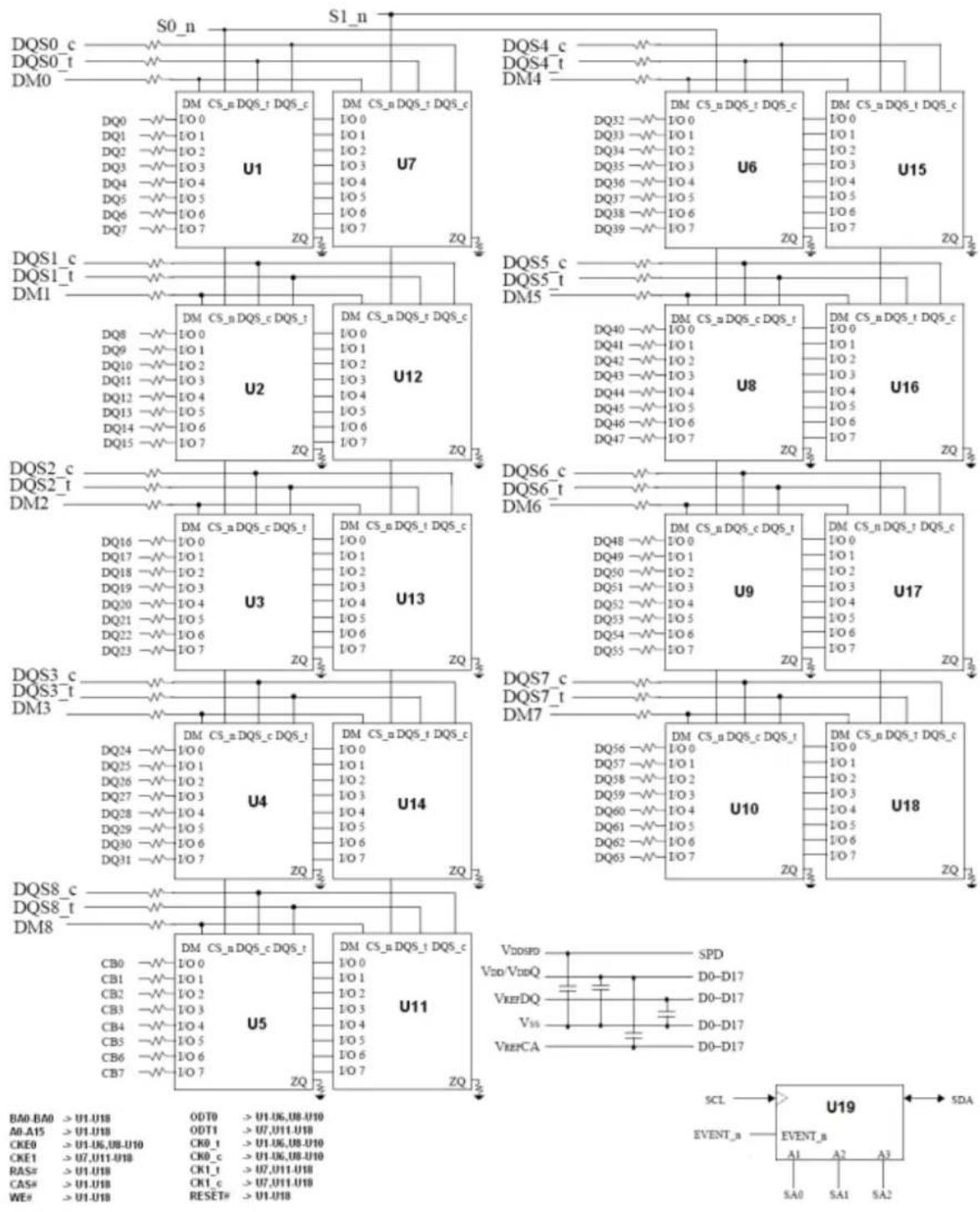
The ADATA's module is a 1024Mx72 bits 8GB(8192MB) DDR3L-1600(CL11)-11-11-28 SDRAM memory module. The SPD is programmed to JEDEC standard latency 1600Mbps timing of 11-11-11-28 at 1.35V. The module is composed of eighteen 512Mx8 bits CMOS DDR3 SDRAMs in FBGA package and one 2Kbit EEPROM in 8pin TDFN package on a 240pin glass—epoxy printed circuit board.
The module is a Dual In-line Memory Module and intended for mounting onto 240 pins edge connector sockets. Synchronous design allows precise cycle control with the use of system clock. Data I/O transactions are possible on both edges of DQS. Range of operating frequencies, programmable latencies and burst lengths allow the same device to be useful for a variety of high bandwidth, high performance memory system applications.
Features :
• Power supply (Normal): VDD & VDDQ = 1.35V ± 0.0675V
• MRS Cycle with address key programs
- CAS Latency (5,6,7,8,9,10,11)
- Burst Length (BL):8 and 4 with Burst Chop(BC)
• Bi-directional, differential data strobe (DQS and /DQS)
- Differential clock input (CK, /CK) operation
- DLL aligns DQ and DQS transition with CK transition
- Double-data-rate architecture; two data transfers per clock cycle
• 8 independent internal bank
- Internal (self) calibration: Internal self calibration through ZQ pin (RZQ:240 ohm±1%)
• Auto refresh and self refresh
• Average Refresh Period 7.8us at lower then TCASE 85°C, 3.9us at 85°C < TCASE ≤ 95°C
- 8-bit pre-fetch.
• Supports ECC error correction and detection.
- On Die Termination using ODT pin.
- On-board I2C temperature sensor with integrated serial presence-detect (SPD) EEPROM.
- Lead-free products are RoHS Compliant
Pin Assignment :
| PIN NAME FUNCTION | ||
| CK0,/CK0CK1,/CK1 | System Clock Active on the positive and negative edge to sample all inputs. | |
| CKE0~CKE1 | Clock Enable least on cycle prior new command. Disable input buffers for power down in standby | |
| /S0-/S1 | Chip | Disables or Enables device operation by masking or enabling all input except CK, CKE and Select L(U)DQM |
| A0~A15 | Address | Row / Column address are multiplexed on the same pins.(Row Address: A0~A14 , Column Address: A0~A9 , Auto precharge: A10/AP) |
| BA0~BA2 | Banks | Selects bank to be activated during row address latch time.Select Selects bank for read / write during column address latch time. |
| CB0~CB7 ECC | Check ECC Check bit | |
| DQ0~DQ63 | Data Data bit inputs / outputs are multiplexed on the same pins. | |
| DQS0~DQS8,/DQS0~/DQS8 | Data Strobe Bi-directional Data Strobe | |
| DM0~DM8 Data | Mask Mask input data when DM is high. | |
| /RAS Row Address Strobe Latches row addresses on the positive edge of the CK with /RAS low | ||
| /CAS | Column Address Strobe | Latches Column addresses on the positive edge of the CK with /CAS low |
| /WE | Write Enable | Enables write operation and row recharge. |
| VDD / VSS | Power Supply/Ground | Power and Ground for the input buffers and the core logic. |
| VREFDQ | Power Supply reference | Power Supply for reference.DQ,DM.VDD/2 |
| VREFCA | Power Supply reference | Power Supply for reference. Command , address, & control.VDD/2 |
| VDDQ | Power Supply | Power supply for the DDR3 SDRAM output buffers to provide improved noise immunity. |
| SDA Serial data I/O EEPROM serial data I/O | ||
| SCL Serial clock EEPROM clock input | ||
| SA0~SA2 Address in EEPROM EEPROM address input | ||
| VDDSPD Power Supply Power supply for SPD EEPROM | ||
| ODT0~ODT1 | On Die | When high, termination resistance is enabled for all DQ, /DQ and DM pins, assuming the Termination function is enabled in the Extended Mode Register Set. |
| /RESET | Reset | /RESET is an active LOW CMOS input referenced to VSS. The RESET# input receiver is a CMOS input defined as a rail-to-rail signal with DC HIGH ≥ 0.8 × VDD and DC LOW ≤ 0.2 × VDD. RESET# assertion and deassertion are asynchronous. |
| /EVENT | Thermal | This signal indicates that a thermal event has been detected in the thermal sensing device. The system should guarantee the electrical level requirement is met for the EVENT pin on TS/SPD part. |
| NC No Connection This pin is recommended to be left No Connection on the device. | ||
Block Diagram :
flowchart
graph TD
    subgraph U1
        U1_1["DM CS_n DQS_t DQS_c"]
        U1_2["DM CS_n DQS_t DQS_c"]
    end
    subgraph U2
        U2_1["DM CS_n DQS_c DQS_t"]
        U2_2["DM CS_n DQS_t DQS_c"]
    end
    subgraph U3
        U3_1["DM CS_n DQS_c DQS_t"]
        U3_2["DM CS_n DQS_t DQS_c"]
    end
    subgraph U4
        U4_1["DM CS_n DQS_c DQS_t"]
        U4_2["DM CS_n DQS_t DQS_c"]
    end
    subgraph U5
        U5_1["DM CS_n DQS_c DQS_t"]
        U5_2["DM CS_n DQS_t DQS_c"]
    end
    subgraph U6
        U6_1["DM CS_n DQS_t DQS_c"]
        U6_2["DM CS_n DQS_t DQS_c"]
    end
    subgraph U7
        U7_1["DM CS_n DQS_t DQS_c"]
        U7_2["DM CS_n DQS_t DQS_c"]
    end
    subgraph U8
        U8_1["DM CS_n DQS_c DQS_t"]
        U8_2["DM CS_n DQS_t DQS_c"]
    end
    subgraph U9
        U9_1["DM CS_n DQS_c DQS_t"]
        U9_2["DM CS_n DQS_t DQS_c"]
    end
    subgraph U10
        U10_1["DM CS_n DQS_c DQS_t"]
        U10_2["DM CS_n DQS_t DQS_c"]
    end
    subgraph U11
        U11_1["DM CS_n DQS_t DQS_c"]
        U11_2["DM CS_n DQS_t DQS_c"]
    end
    subgraph U19
        U19_1["VDDSPD"]
        U19_2["VDDVDDQ"]
        U19_3["VREFDQ"]
        U19_4["VSS"]
        U19_5["VREFCA"]
    end

    A["S0_n"] --> B["S1_n"]
    C["DQSO c"] --> A
    D["DQSO t"] --> A
    E["DM0"] --> A
    F["DQ0"] --> A
    G["DQ1"] --> A
    H["DQ2"] --> A
    I["DQ3"] --> A
    J["DQ4"] --> A
    K["DQ5"] --> A
    L["DQ6"] --> A
    M["DQ7"] --> A
    N["DQ8"] --> A
    O["DQ9"] --> A
    P["DQ10"] --> A
    Q["DQ11"] --> A
    R["DQ12"] --> A
    S["DQ13"] --> A
    T["DQ14"] --> A
    U["DQ15"] --> A
    V["DQ23"] --> A
    W["DQ31"] --> A
    X["DQ30"] --> A
    Y["DQ39"] --> A
    Z["SCL"] --> AA["U19"]
    AB["SCL"] --> AC["U19"]
    AD["SCL"] --> AE["U19"]

    style U1 fill:#f9f,stroke:#333,stroke-width:2px
    style U2 fill:#f9f,stroke:#333,stroke-width:2px
    style U3 fill:#f9f,stroke:#333,stroke-width:2px
    style U4 fill:#f9f,stroke:#333,stroke-width:2px
    style U5 fill:#f9f,stroke:#333,stroke-width:2px
    style U6 fill:#f9f,stroke:#333,stroke-width:2px
    style U7 fill:#f9f,stroke:#333,stroke-width:2px
    style U8 fill:#f9f,stroke:#333,stroke-width:2px
    style U9 fill:#f9f,stroke:#333,stroke-width:2px
    style U10 fill:#f9f,stroke:#333,stroke-width:2px
    style U11 fill:#f9f,stroke:#333,stroke-width:2px

    note right of A,B,C,D,E,F,G,H,I,J,K,L,M,N,P,Q,R,S,T,U,V,W,X,Y,Z,Z,Z,Z,Z,Z,Z,Z,Z,Z,Z,Z,Z,Z,Z,Z,Z,Z,Z,Z,Z,Z,Z,Z,Z,Z,Z,Z,Z,Z,Z,Z,Z,Z,Z,Z,Z,Z,Z,Z,Z,Z,Z,Z,Z,Z,Z,Z,Z,Z,Z,Z,Z,Z,Z,Z,Z,Z,Z,Z,Z,Z,Z,Z,Z,Z,Z,Z,Z,Z,Z,Z,Z,Z,Z,Z,Z,Z,Z,Z,Z,Z,Z,Z,Z,Z,Z,Z,Z,Z,Z,Z,Z,Z,Z,Z,Z,Z,Z,Z,z,A,B,C,D,E,F,G,H,I,J,K,L,M,N,P,Q,R,S,T,U,V,W,X,Y,Z,X,Y,z,X,Y,z,X,Y,z,X,Y,z,X,Y,z,X,Y,z,X,Y,z,X,Y,z,X,Y,z,X,Y,z,X,Y,z,X,Y,z,X,Y,z,X,Y,z,X,Y,z,X,Y,z,X,Y,z,X,Y,z,X,Y,z,X,Y,z,X,Y,z,X,Y,z,X,Y,z,X,Y,z,X,Y,z,X,Y,z,X,Y,z,X,Y,z,X,Y,z,X,Y,z,X,Y,z,X,Y,z,X,Y,z,X,Y,z,x,y,z,y,z,y,z,y,z,y,z,y,z,y,z,y,z,y,z,y,z,y,z,y,z,y,z,y,z,y,z,y,z,y,z,y,z,y,z,y,z,y,z,y,z,y,z,y,z,y,z,y,z,y,z,y,z,y,z,y,z,y,z,y,z,y,z,y,z,y,z,y,z,y,z,y,z,y,z,y,z,y,z,y,z,y,z,y,z,y,z,y,z,y,z,y,z,y,z,y,z,y-z,a,b,c,d,e,f,g,h,i,j,k,l,m,n,o,r,s,t,u,v,w,v,w,x,v,w,v,w,v,w,v,w,v,w,v,w,v,w,v,w,v,w,v,w,v,w,v,w,v,w,v,w,v,w,v,w,v,w,v,w,v,w,v,w,v,w,v,w,v,w,v,w,v,w,v,w,v,w,v,w,v,w,v,w,v,w,v,w,v,w,v,w,v,w,v,w,v,w,v,w,v,w,v,w,v,w,v,w,v,w,v,w,v,w,v,w,v,w,v,w,v,w,v,w,v,m,n,n,n,n,n,n,n,n,n,n,n,n,n,n,n,n,n,n,n,n,n,n,n,n,n,n,n,n,n,n,n,n,n,n,n,n,n,n,n,n,n,n,n,n,n,n,n,n,n,n,n,n,n,n,n,n,n,n,n,n,n,n,n,n,n,n,n,n,n,n,n,n,n,n,n,n,n,n,n,n,n,n,n,n,n,n,n,n,n,n,n,n,n,n,n,n,n,n,n,n,,n,,n,,n,,n,,n,,n,,n,,n,,n,,n,,n,,n,,n,,n,,n,,n,,n,,n,,n,,n,,n,,n,,n,,n,,n,,n,,n,,n,,n,,n,,n,,n,,n,,n,,n,,n,,n,,n,,n,,n,,n,,n,,n,,n,,n,,n,,n,,n,,n,,n,,N,B,C,D,E,F,G,H,I,J,K,l,m,m,n,o,r,s,t,u,v,w,x,x,x,x,x,x,x,x,x,x,x,x,x,x,x,x,x,x,x,x,x,x,x,x,x,x,x,x,x,x,x,x,x,x,x,x,x,x,x,x,x,x,x,x,x,x,x,x,x,x,x,x,x,x,x,x,x,x,x,x,x,x,x,x,x,x,x,x,x,x,x,x,x,x,x,x,x,x,x,x,x,x,x,x,x,x,x,x,x,x,x,x,x,x,x,x,x,x,x,x,t,N,B,C,D,E,F,G,H,I,J,K,l,m,m,m,m,m,m,m,m,m,m,m,m,m,m,m,m,m,m,m,m,m,m,m,m,m,m,m,m,m,m,m,m,m,m,m,m,m,m,m,m,m,m,m,m,m,m,m,m,m,m,m,m,m,m,m,m,m,m,m,m,m,m,m,m,m,m,m,m,m,m,m,m,m,m,m,m,m,m,m,m,m,m,m,m,m,m,m,m,m,m,m,m,m,m,m,m,m,m,m,mm,k,l,k,l,k,l,k,l,k,l,k,l,k,l,k,l,k,l,k,l,k,l,k,l,k,l,k,l,k,l,k,l,k,l,k,l,k,l,k,l,k,l,k,l,k,l,k,l,k,l,k,l,k,l,k,l,k,l,k,l,k,l,k,l,k,l,k,l,k,l,k,l,k,l,k,l,k,l,k,l,k,l,k,l,k,l,k,l,k,l,k,l,k,l,k,l,k,l,k,l,kl,k,l,k,l,k,l,k,l,k,l,k,l,k,l,k,l,k,l,k,l,k,l,k,l,k,l,k,l,k,l,k,l,k,l,k,l,k,l,k,l,k,l,k,l,k,l,k,l,k,l,k,l,k,l,k,l,k,l,k,l,k,l,k,l,k,l,k,l,k,l,k,l,k,l,k,l,k,l,k,l,k,l,k,l,k,l,k,l,k,l,k,l,k,l,k,l,k,l,k{l},
Absolute Maximum Ratings :
| Parameter Symbol Value | Unit | ||
| Voltage on VDD supply relative to Vss VDD | -0.4 ~ 1.975 V | ||
| Voltage on VDDQ pin relative to Vss VDDQ | -0.4 ~1.975 V | ||
| Voltage on any pin relative to Vss VIN, Vout | -0.4 ~ 1.975 V | ||
| Storage temperature TStg -55 ~ +100 | °C |
Note: DDR3 SDRAM component specification.
Operation Temperature Condition
| Parameter | Symbol | Value | Unit | Note |
| Normal Operating Temperature Range | TC | 0~+85 | °C | 1 |
| Extended Temperature Range (Optional) | TC | +85~+95 | °C | 1 |
Note: (1) If the DRAM case temperature is above 85 °C, the Auto-Refresh command interval has to be reduced to tREFI=3.9us.
DC Operating Condition :
Voltage referenced to Vss = 0V, VDD&VDDQ=1.35V±0.0675V, Tc = 0 to 85 °C
| Parameter | Symbol | Min | Max | Unit | Note |
| Supply Voltage | VDD | 1.283 | 1.45 | V | 1,2 |
| VDDSPD | 3 | 3.6 | V | ||
| Supply Voltage for Output | VDDQ | 1.283 | 1.45 | V | 1,2 |
| I/O Reference Voltage(CMD/ADD) | VREFCA, (DC) | 0.49 x VDDQ | 0.51 x VDDQ | V | 3,4 |
| I/O Reference Voltage(DQ) | VREFDQ, (DC) | 0.49 x VDDQ | 0.51 x VDDQ | V | 3,4 |
| Termination Voltage | VTT | VDDQ/2 - TBD | VDDQ/2 +TBD | V |
Note: (1) Under all conditions VDDQ must be less than or equal to VDD.
(2) VDDQ tracks with VDD. AC parameters are measured with VDD and VDDQ tied together.
(3) The AC peak noise on VREF may not allow VREF to deviate from VREF(DC) by more than ±1% VDD
(for reference: approx. ±13.5mV)
(4) For reference: approx. VDD/2 ±13.5mV
Input DC & AC Logic Level for single-ended signals :
| Parameter | Symbol | Min | Max | Unit | Note |
| DC Input logic high voltage | VIH (DC) | VREF+90 | VDD | mV | 1 |
| DC Input logic low voltage VIL (DC) VSS VREF-90 mV 1 | |||||
| AC input logic high | VIH(AC) | VREF + 160 | - | mV | 1,2 |
| AC input logic low | VIL(AC) | - | VREF - 160 | mV | 1,2 |
Note: 1. For DQ and DM, VREF = VREFDQ. For input only pins except RESET, or VREF = VREFCA.
2. See "Overshoot and Undershoot specifications" on component datasheet
Definition of differential ac-swing and "time above ac level tDVAC
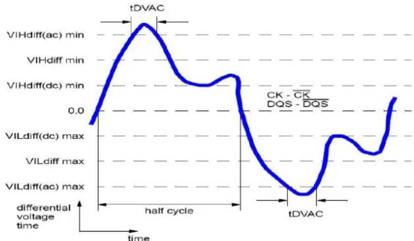
line
| Time Segment | Voltage (arcsec) | |----------------------|------------------| | Half cycle | 1.5 | | tDVAC | 0.0 | | tDVAC (CK - CK / DQS - DQS) | -0.5 |Input AC Logic Level for single-ended signals :
| Parameter | Symbol | Min | Max | Unit | Note |
| Differential input high | VIHdiff | +0.18 | Note 3 | V | 1 |
| Differential input low | VILdiff | Note 3 | -0.18 | V | 1 |
| Differential input high AC | VIHdiff(AC) | 2 (VIH(ac)-Vref) | Note 3 | V | 2 |
| Differential input low AC | VILdiff (AC) | Note 3 | 2 x (VIL(ac) - Vref) | V | 2 |
Notes: 1. Used to define a differential signal slew-rate.
-
For CK - CK use VIH/VIL(ac) of ADD/CMD and VREFCA; for DQS - DQS, DQSL - DQSL, DQSU - DQSU use VIH/VIL(ac) of DQs and VREFDQ; if a reduced ac-high or ac-low level is used for a signal group, then the reduced level applies also here.
-
These values are not defined, however they single-ended signals CK, /CK, DQS, /DQS, DQSL, /DQSL, DQSU, /DQSU need to be within the respective limits (VIH(dc) max, VIL(dc)min) for single-ended signals as well as the limitations for overshoot and undershoot on Component Datasheet.
IDD Specification :
| Symbol | Condition | ||
| IDD0 Operating One Bank Active-Precharge Current 639 mA | |||
| IDD1 Operating One Bank Active-Read-Precharge Current 738 mA | |||
| IDD2P0 Precharge Power-Down Current Slow Exit 288 mA | |||
| IDD2P1 Precharge Power-Down Current Fast Exit 576 mA | |||
| IDD2Q Precharge Quiet Standby Current 486 mA | |||
| IDD2N | Precharge Standby Current 504 mA | ||
| IDD3P | Active Power-Down Current | 684 | mA |
| IDD3N | Active Standby Current | 684 | |
| IDD4W | Operating Burst Write Current | 1269 | mA |
| IDD4R | Operating Burst Read Current | 1557 | mA |
| IDD5B | Burst Refresh Current | 1539 | mA |
| IDD6 Self Refresh Current: Normal Temperature Range | 360 mA | ||
| IDD7 | Operating Bank Interleave Read Current | 2124 | mA |
| IDD8 | Reset Current | 324 | mA |
Speed Bins and CL,tRCD,tRP,tRC and tRAS for Corresponding Bin :
| Speed | DDR3L-1600 | Units |
| Bin(CL-tRCD-tRP) | 11-11-11 | |
| Parameter | min | |
| CL | 11 | tCK |
| tRCD | 13.125 | ns |
| tRC | 48.125 | ns |
| tRRD | 6 | ns |
| tCK | 1.25 | ns |
| tRAS | 35 | ns |
| tRP | 13.125 | ns |
| tRFC | 160 | ns |
Timing Parameters: