
E3-1220L - Processor INTEL - Free user manual and instructions
Find the device manual for free E3-1220L INTEL in PDF.


| Product Type | Processor (CPU) |
| Brand | Intel |
| Model | Xeon E3-1220L |
| Family | Intel Xeon E3-1200 Family |
| Socket | LGA1155 |
| Core Count | 2 |
| Thread Count | 4 (via Hyper-Threading) |
| Base Frequency | 2.2 GHz |
| Cache | 3 MB Intel Smart Cache |
| Thermal Design Power (TDP) | 20 W |
| Manufacturing Technology | 32 nm |
| Memory Support | DDR3-1333, ECC capable |
| Integrated Graphics | No |
| Virtualization | Intel VT-x, VT-d |
| Security Features | Intel TXT, Execute Disable Bit |
| Max Memory Size | 32 GB |
| Operating Temperature Range | 0°C to 69°C (typical) |
| Cooling Requirements | Active heatsink recommended for server environments |
| Dimensions (typical) | 37.5 mm x 37.5 mm |
| Weight (typical) | ~10 g |
Frequently Asked Questions - E3-1220L INTEL
User questions about E3-1220L INTEL
0 question about this device. Answer the ones you know or ask your own.
Ask a new question about this device
Download the instructions for your Processor in PDF format for free! Find your manual E3-1220L - INTEL and take your electronic device back in hand. On this page are published all the documents necessary for the use of your device. E3-1220L by INTEL.
USER MANUAL E3-1220L INTEL
Intel® Xeon® Processor E3-1200 Family
Datasheet, Volume 2
This is Volume 2 of 2
June 2011
INFORMATION IN THIS DOCUMENT IS PROVIDED IN CONNECTION WITH INTEL® PRODUCTS. NO LICENSE, EXPRESS OR IMPLIED, BY ESTOPPEL OR OTHERWISE, TO ANY INTELLECTUAL PROPERTY RIGHTS IS GRANTED BY THIS DOCUMENT. EXCEPT AS PROVIDED IN INTEL'S TERMS AND CONDITIONS OF SALE FOR SUCH PRODUCTS, INTEL ASSUMES NO LIABILITY WHATSOEVER, AND INTEL DISCLAIMS ANY EXPRESS OR IMPLIED WARRANTY, RELATING TO SALE AND/OR USE OF INTEL PRODUCTS INCLUDING LIABILITY OR WARRANTIES RELATING TO FITNESS FOR A PARTICULAR PURPOSE, MERCHANTABILITY, OR INFRINGEMENT OF ANY PATENT, COPYRIGHT OR OTHER INTELLECTUAL PROPERTY RIGHT. Intel products are not intended for use in medical, life saving, life sustaining, critical control or safety systems, or in nuclear facility applications.
Intel may make changes to specifications and product descriptions at any time, without notice.
Designers must not rely on the absence or characteristics of any features or instructions marked "reserved" or "undefined." Intel reserves these for future definition and shall have no responsibility whatsoever for conflicts or incompatibilities arising from future changes to them.
The products described in this document may contain design defects or errors known as errata which may cause the product to deviate from published specifications. Current characterized errata are available on request.
Intel processor numbers are not a measure of performance. Processor numbers differentiate features within each processor family, not across different processor families. See http://www.intel.com/products/processor_number for details. Over time processor numbers will increment based on changes in clock, speed, cache, FSB, or other features, and increments are not intended to represent proportional or quantitative increases in any particular feature. Current roadmap processor number progression is not necessarily representative of future roadmaps. See www.intel.com/products/processor_number for details.
No computer system can provide absolute security under all conditions. Intel ^® Trusted Execution Technology (Intel ^® TXT) requires a computer system with Intel ^® Virtualization Technology, an Intel TXT-enabled processor, chipset, BIOS, Authenticated Code Modules and an Intel TXT-compatible measured launched environment (MLE). The MLE could consist of a virtual machine monitor, an OS or an application. In addition, Intel TXT requires the system to contain a TPM v1.2, as defined by the Trusted Computing Group and specific software for some uses. For more information, see http://www.intel.com/technology/security/.
Intel® Virtualization Technology requires a computer system with an enabled Intel® processor, BIOS, virtual machine monitor (VMM) and, for some uses, certain platform software enabled for it. Functionality, performance or other benefits will vary depending on hardware and software configurations and may require a BIOS update. Software applications may not be compatible with all operating systems. Please check with your application vendor.
Intel® Active Management Technology (Intel® AMT) requires the computer system to have an Intel® AMT-enabled chipset, network hardware and software, as well as connection with a power source and a corporate network connection. Setup requires configuration by the purchaser and may require scripting with the management console or further integration into existing security frameworks to enable certain functionality. It may also require modifications of implementation of new business processes. With regard to notebooks, Intel AMT may not be available or certain capabilities may be limited over a host OS-based VPN or when connecting wirelessly, on battery power, sleeping, hibernating or powered off. For more information, see http://www.intel.com/technology/platform-technology/intel-amt/
Enabling Execute Disable Bit functionality requires a PC with a processor with Execute Disable Bit capability and a supporting operating system. Check with your PC manufacturer on whether your system delivers Execute Disable Bit functionality.
Contact your local Intel sales office or your distributor to obtain the latest specifications and before placing your product order.
Copies of documents which have an order number and are referenced in this document, or other Intel literature may be obtained by calling 1-800-548-4725 or by visiting Intel's website at http://www.intel.com.
Intel, Intel Core, Intel Xeon, and the Intel logo are trademarks of Intel Corporation in the U. S. and other countries.
* Other names and brands may be claimed as the property of others.
Copyright © 2011 Intel Corporation. All Rights Reserved.
Contents
1 Introduction....11
2 Processor Configuration Registers....13
2.1 Register Terminology 13
2.2 PCI Devices and Functions on Processor 14
2.3 System Address Map 15
2.3.1 Legacy Address Range 18
2.3.1.1 DOS Range (0h-9_FFFFh).... 18
2.3.1.2 Legacy Video Area (A_0000h-B_FFFFh) 19
2.3.1.3 PAM (C 0000h-F FFFFh) 20
2.3.2 Main Memory Address Range (1 MB - TOLUD) 20
2.3.2.1 ISA Hole (15 MB-16 MB) 21
2.3.2.2 TSEG 21
2.3.2.3 Protected Memory Range (PMR) - (programmable) 21
2.3.2.4 DRAM Protected Range (DPR) 22
2.3.2.5 Pre-allocated Memory 22
2.3.2.6 GFX Stolen Spaces.... 23
2.3.2.7 ME UMA 23
2.3.3 PCI Memory Address Range (TOLUD - 4 GB).... 23
2.3.3.1 APIC Configuration Space (FEC0_0000h-FECF_FFFFh) 25
2.3.3.2 HSEG (FEDA_0000h-FEDB_FFFFh) 25
2.3.3.3 MSI Interrupt Memory Space (FEE0_0000h-FEEF_FFFFh).... 25
2.3.3.4 High BIOS Area 25
2.3.4 Main Memory Address Space (4 GB to TOUUD) 26
2.3.4.1 Memory Re-claim Background 27
2.3.4.2 Indirect Accesses to MCHBAR Registers.... 27
2.3.4.3 Memory Remapping 28
2.3.4.4 Hardware Remap Algorithm.... 28
2.3.4.5 Programming Model 28
2.3.5 PCI Express* Configuration Address Space 32
2.3.6 PCI Express* Graphics Attach (PEG) 33
2.3.7 Graphics Memory Address Ranges 34
2.3.7.1 IOBAR Mapped Access to Device 2 MMIO Space 34
2.3.7.2 Trusted Graphics Ranges 34
2.3.8 System Management Mode (SMM) 35
2.3.9 SMM and VGA Access through GTT TLB 35
2.3.10 ME Stolen Memory Accesses 35
2.3.11 I/O Address Space 36
2.3.11.1 PCI Express* I/O Address Mapping.... 36
2.3.12 MCTP and KVM Flows 37
2.3.13 Decode Rules and Cross-Bridge Address Mapping 37
2.3.13.1 DMI Interface Decode Rules 37
2.3.13.2 PCI Express* Interface Decode Rules.... 40
2.3.13.3 Legacy VGA and I/O Range Decode Rules.... 41
2.4 Processor Register Introduction.... 45
2.4.1 I/O Mapped Registers 46
2.5 PCI Device 0, Function 0 Configuration Registers 46
2.5.1 VID—Vendor Identification Register 48
2.5.2 DID—Device Identification Register 48
2.5.3 PCICMD—PCI Command Register 49
2.5.4 PCISTS—PCI Status Register 50
2.5.5 RID—Revision Identification Register 52
2.5.6 CC—Class Code Register 53
2.5.7 HDR—Header Type Register.... 53
2.5.8 SVID—Subsystem Vendor Identification Register 54
2.5.9 SID—Subsystem Identification Register 54
2.5.10 PXPEPBAR—PCI Express Egress Port Base Address Register....55
2.5.11 MCHBAR—Host Memory Mapped Register Range Base Register .....56
2.5.12 GGC—GMCH Graphics Control Register Register....57
2.5.13 DEVEN—Device Enable Register....59
2.5.14 PCIEXBAR—PCI Express Register Range Base Address Register....60
2.5.15 DMIBAR—Root Complex Register Range Base Address Register....62
2.5.16 PAM0—Programmable Attribute Map 0 Register 63
2.5.17 PAM1—Programmable Attribute Map 1 Register 64
2.5.18 PAM2—Programmable Attribute Map 2 Register 65
2.5.19 PAM3—Programmable Attribute Map 3 Register 66
2.5.20 PAM4—Programmable Attribute Map 4 Register 67
2.5.21 PAM5—Programmable Attribute Map 5 Register 68
2.5.22 PAM6—Programmable Attribute Map 6 Register 69
2.5.23 LAC—Legacy Access Control Register....70
2.5.24 REMAPBASE—Remap Base Address Register....74
2.5.25 REMAPLIMIT—Remap Limit Address Register 74
2.5.26 TOM—Top of Memory Register....75
2.5.27 TOUUD—Top of Upper Usable DRAM Register 76
2.5.28 BDSM—Base Data of Stolen Memory Register 77
2.5.29 BGSM—Base of GTT stolen Memory Register 77
2.5.30 G Memory Base Register....78
2.5.31 TOLUD—Top of Low Usable DRAM Register....78
2.5.32 ERRSTS—Error Status Register....80
2.5.33 ERRCMD—Error Command Register....81
2.5.34 SMI Command Register 81
2.5.35 SCICMD—SCI Command Register 82
2.5.36 SKPD—Scratchpad Data Register 82
2.5.37 CAPID0_A—Capabilities A Register....83
2.6 PCI Device 1, Function 0-2 Configuration Registers 85
2.6.1 VID1—Vendor Identification Register....87
2.6.2 DID1—Device Identification Register 87
2.6.3 PCICMD1—PCI Command Register 88
2.6.4 PCISTS1—PCI Status Register 90
2.6.5 RID1—Revision Identification Register 92
2.6.6 CC1—Class Code Register 92
2.6.7 CL1—Cache Line Size Register....93
2.6.8 HDR1—Header Type Register 93
2.6.9 PBUSN1—Primary Bus Number Register....93
2.6.10 SBUSN1—Secondary Bus Number Register....94
2.6.11 SUBUSN1—Subordinate Bus Number Register 94
2.6.12 IOBASE1—I/O Base Address Register 95
2.6.13 IOLIMIT1—I/O Limit Address Register 95
2.6.14 SSTS1—Secondary Status Register 96
2.6.15 MBASE1—Memory Base Address Register....97
2.6.16 MLIMIT1—Memory Limit Address Register....98
2.6.17 PMBASE1—Prefetchable Memory Base Address Register 99
2.6.18 PMLIMIT1—Prefetchable Memory Limit Address Register 100
2.6.19 PMBASEU1—Prefetchable Memory Base Address Upper Register 101
2.6.20 PMLIMITU1—Prefetchable Memory Limit Address Upper Register 102
2.6.21 CAPPTR1—Capabilities Pointer Register....102
2.6.22 INTRLINE1—Interrupt Line Register 103
2.6.23 INTRPIN1—Interrupt Pin Register.... 103
2.6.24 BCTRL1—Bridge Control Register 104
2.6.25 PM_CAPID1—Power Management Capabilities Register 106
2.6.26 PM CS1—Power Management Control/Status Register.... 107
2.6.27 SS_CAPID—Subsystem ID and Vendor ID Capabilities Register.... 108
2.6.28 SS—Subsystem ID and Subsystem Vendor ID Register.... 109
2.6.29 MSI_CAPID—Message Signaled Interrupts Capability ID Register 109
2.6.30 MC—Message Control Register 110
2.6.31 MA—Message Address Register 111
2.6.32 MD—Message Data Register 111
2.6.33 PEG_CAPL—PCI Express-G Capability List Register.... 111
2.6.34 PEG_CAP—PCI Express-G Capabilities Register.... 112
2.6.35 DCAP—Device Capabilities Register.... 112
2.6.36 DCTL—Device Control Register 113
2.6.37 DSTS—Device Status Register 114
2.6.38 LCTL—Link Control Register.... 115
2.6.39 LSTS—Link Status Register.... 117
2.6.40 SLOTCAP—Slot Capabilities Register 118
2.6.41 SLOTCTL—Slot Control Register 120
2.6.42 SLOTSTS—Slot Status Register 122
2.6.43 RCTL—Root Control Register.... 124
2.6.44 LCTL2—Link Control 2 Register 125
2.7 PCI Device 1, Function 0-2 Extended Configuration Registers.... 127
2.7.1 PVCCAP1—Port VC Capability Register 1 127
2.7.2 PVCCAP2—Port VC Capability Register 2 128
2.7.3 PVCCTL—Port VC Control Register 128
2.7.4 VC0RCAP—VC0 Resource Capability Register.... 129
2.7.5 VC0RCTL—VC0 Resource Control Register.... 130
2.7.6 VC0RSTS—VC0 Resource Status Register 131
2.7.7 PEG_TC—PCI Express Completion Time-out Register.... 131
2.8 PCI Device 2 Configuration Registers 132
2.8.1 VID2—Vendor Identification Register 133
2.8.2 DID2—Device Identification Register.... 133
2.8.3 PCICMD2—PCI Command Register.... 134
2.8.4 PCISTS2—PCI Status Register.... 135
2.8.5 RID2—Revision Identification Register.... 136
2.8.6 CC—Class Code Register 136
2.8.7 CLS—Cache Line Size Register 137
2.8.8 MTXT2—Master Latency Timer Register 137
2.8.9 HDR2—Header Type Register.... 137
2.8.10 GTTMMADR—Graphics Translation Table, Memory Mapped Range Address Register.... 138
2.8.11 GMADR—Graphics Memory Range Address Register 139
2.8.12 IOBAR—I/O Base Address Register 140
2.8.13 SVID2—Subsystem Vendor Identification Register 140
2.8.14 SID2—Subsystem Identification Register 141
2.8.15 ROMADR—Video BIOS ROM Base Address Register 141
2.8.16 INTRPIN—Interrupt Pin Register.... 141
2.8.17 MINGNT—Minimum Grant Register 142
2.8.18 MAXLAT—Maximum Latency Register 142
2.8.19 MSAC—Multi Size Aperture Control Register.... 143
2.9 Device 2 I/O Registers 144
2.9.1 INDEX—MMIO Address Register 144
2.9.2 DATA—MMIO Data Register 144
2.10 PCI Device 6 Configuration Registers 145
2.10.1 VID6—Vendor Identification Register 146
2.10.2 DID6—Device Identification Register.... 147
2.10.3 PCICMD6—PCI Command Register.... 147
2.10.4 PCISTS6—PCI Status Register 149
2.10.5 RID6—Revision Identification Register 151
2.10.6 CC6—Class Code Register 151
2.10.7 CL6—Cache Line Size Register....152
2.10.8 HDR6—Header Type Register 152
2.10.9 PBUSN6—Primary Bus Number Register....152
2.10.10 SBUSN6—Secondary Bus Number Register....153
2.10.11 SUBUSN6—Subordinate Bus Number Register 153
2.10.12 IOBASE6—I/O Base Address Register 154
2.10.13 IOLIMIT6—I/O Limit Address Register 154
2.10.14 SSTS6—Secondary Status Register 155
2.10.15 MBASE6—Memory Base Address Register....156
2.10.16 MLIMIT6—Memory Limit Address Register 157
2.10.17 PMBASE6—Prefetchable Memory Base Address Register 158
2.10.18 PMLIMIT6—Prefetchable Memory Limit Address Register 159
2.10.19 PMBASEU6—Prefetchable Memory Base Address Upper Register....160
2.10.20 PMLIMITU6—Prefetchable Memory Limit Address Upper Register .....161
2.10.21 CAPPTR6—Capabilities Pointer Register.... 161
2.10.22 INTRLINE6—Interrupt Line Register 162
2.10.23 INTRPIN6—Interrupt Pin Register....162
2.10.24 BCTRL6—Bridge Control Register 163
2.10.25 PM_CAPID6—Power Management Capabilities Register 165
2.10.26 PM_CS6—Power Management Control/Status Register 166
2.10.27 SS_CAPID—Subsystem ID and Vendor ID Capabilities Register .....167
2.10.28 SS—Subsystem ID and Subsystem Vendor ID Register 168
2.10.29 MSI_CAPID—Message Signaled Interrupts Capability ID Register .....168
2.10.30 MC—Message Control Register.... 169
2.10.31 MA—Message Address Register....170
2.10.32 MD—Message Data Register 170
2.10.33 PEG_CAPL—PCI Express-G Capability List Register 170
2.10.34 PEG_CAP—PCI Express-G Capabilities Register 171
2.10.35 DCAP—Device Capabilities Register 171
2.10.36 DCTL—Device Control Register 172
2.10.37 DSTS—Device Status Register 173
2.10.38 LCTL—Link Control Register 174
2.10.39 LSTS—Link Status Register 176
2.10.40 SLOTCAP—Slot Capabilities Register....177
2.10.41 SLOTCTL—Slot Control Register.... 179
2.10.42 SLOTSTS—Slot Status Register....181
2.10.43 RCTL—Root Control Register 182
2.11 PCI Device 6 Extended Configuration Registers 183
2.11.1 PVCCAP1—Port VC Capability Register 1 183
2.11.2 PVCCAP2—Port VC Capability Register 2 ....184
2.11.3 PVCCTL—Port VC Control Register....184
2.11.4 VC0RCAP—VC0 Resource Capability Register 185
2.11.5 VC0RCTL—VC0 Resource Control Register 186
2.11.6 VC0RSTS—VC0 Resource Status Register....187
2.12 DMIBAR Registers.... 188
2.12.1 DMIVCECH—DMI Virtual Channel Enhanced Capability Register....189
2.12.2 DMIPVCCAP1—DMI Port VC Capability Register 1 ....190
2.12.3 DMIPVCCAP2—DMI Port VC Capability Register 2 190
2.12.4 DMIPVCCTL—DMI Port VC Control Register....191
2.12.5 DMI VC0RCAP—DMI VC0 Resource Capability Register....191
2.12.6 DMI VC0RCTL—DMI VC0 Resource Control Register....192
2.12.7 DMIVC0RSTS—DMI VC0 Resource Status Register....193
2.12.8 DMI VC1 RCAP—DMI VC1 Resource Capability Register....193
2.12.9 DMIVC1RCTL—DMI VC1 Resource Control Register 194
2.12.10 DMI VC1RSTS—DMI VC1 Resource Status Register 195
2.12.11 DMI VCPRCAP—DMI VCP Resource Capability Register.... 195
2.12.12 DMI VCPRCTL—DMI VCp Resource Control Register 196
2.12.13 DMI VCPRSTS—DMI VCP Resource Status Register 197
2.12.14 DMI ESD—DMI Element Self Description Register 198
2.12.15 DMILE1D—DMI Link Entry 1 Description Register.... 199
2.12.16 DMILE1A—DMI Link Entry 1 Address Register.... 199
2.12.17 DMILE2D—DMI Link Entry 2 Description Register.... 200
2.12.18 DMILE2A—DMI Link Entry 2 Address Register.... 200
2.12.19 LCAP—Link Capabilities Register.... 201
2.12.20 LCTL—Link Control Register 202
2.12.21 LSTS—DMI Link Status Register 203
2.12.22 LCTL2—Link Control 2 Register 204
2.12.23 LSTS2—Link Status 2 Register 206
2.12.24 AFE_BMUFO—AFE BMU Configuration Function 0 Register 206
2.12.25 AFE_BMUTO—AFE BMU Configuration Test 0 Register 206
2.13 MCHBAR Registers in Memory Controller – Channel 0 207
2.13.1 TC_DBP_C0—Timing of DDR Bin Parameters Register.... 207
2.13.2 TC_RAP_C0—Timing of DDR Regular Access Parameters Register 208
2.13.3 SC_IO_LATENCY_C0—IO Latency Configuration Register 208
2.13.4 TC_SRFTP_C0—Self-Refresh Timing Parameters Register.... 209
2.13.5 PM_PDWN_config_C0—Power-down Configuration Register 209
2.13.6 ECCERRLOG0_C0—ECC Error Log 0 Register 210
2.13.7 ECCERRLOG1_C0—ECC Error Log 1 Register 210
2.13.8 TC_RFP_C0—Refresh Parameters Register 211
2.13.9 TC_RFTP_C0—Refresh Timing Parameters Register 211
2.14 MCHBAR Registers in Memory Controller - Channel 1 212
2.14.1 TC_DBP_C1—Timing of DDR Bin Parameters Register.... 212
2.14.2 TC_RAP_C1—Timing of DDR Regular Access Parameters Register 213
2.14.3 SC_IO_LATENCY_C1—IO Latency Configuration Register 213
2.14.4 TC_SRFTP_C1—Self-Refresh Timing Parameters Register.... 214
2.14.5 PM_PDWN_Config_C1—Power-down Configuration Register.... 214
2.14.6 ECCERRLOG0_C1—ECC Error Log 0 Register 215
2.14.7 ECCERRLOG1_C1—ECC Error Log 1 Register 215
2.14.8 TC_RFP_C1—Refresh Parameters Register 216
2.14.9 TC_RFTP_C1—Refresh Timing Parameters Register 216
2.15 MCHBAR Registers in Memory Controller – Integrated Memory Peripheral Hub (IMPH) 217
2.15.1 CRDTCTL3—Credit Control 3 Register.... 217
2.16 MCHBAR Registers in Memory Controller – Common.... 218
2.16.1 MAD_CHNL—Address Decoder Channel Configuration Register.... 218
2.16.2 MAD_DIMM_ch0—Address Decode Channel 0 Register.... 219
2.16.3 MAD_DIMM_ch1—Address Decode Channel 1 Register.... 220
2.16.4 PM_SREF_config—Self Refresh Configuration Register 221
2.17 Memory Controller MMIO Registers Broadcast Group 222
2.17.1 PM_PDWN_Config—Power-down Configuration Register.... 222
2.17.2 ECCERRLOG0—ECC Error Log 0 Register 223
2.17.3 ECCERRLOG1—ECC Error Log 1 Register 223
2.17.4 PM_CMD_PWR—Power Management Command Power Register.... 224
2.17.5 PM_BW_LIMIT_config—BW Limit Configuration Register 224
2.18 Integrated Graphics VT-d Remapping Engine Registers.... 225
2.18.1 VER_REG—Version Register.... 226
2.18.2 CAP_REG—Capability Register.... 227
2.18.3 ECAP_REG—Extended Capability Register 230
2.18.4 GCMD_REG—Global Command Register 232
2.18.5 GSTS_REG—Global Status Register 235
2.18.6 RTADDR_REG—Root-Entry Table Address Register 236
2.18.7 CCMD_REG—Context Command Register 237
2.18.8 FSTS_REG—Fault Status Register 239
2.18.9 FECTL_REG—Fault Event Control Register 241
2.18.10 FEDATA_REG—Fault Event Data Register 242
2.18.11 FEADDR_REG—Fault Event Address Register 242
2.18.12 FEUADDR_REG—Fault Event Upper Address Register 242
2.18.13 AFLOG_REG—Advanced Fault Log Register....243
2.18.14 PMEN_REG—Protected Memory Enable Register 244
2.18.15 PLMBASE_REG—Protected Low-Memory Base Register....245
2.18.16 PLMLIMIT_REG—Protected Low-Memory Limit Register 246
2.18.17 PHMBASE_REG—Protected High-Memory Base Register 247
2.18.18 PHMLIMIT_REG—Protected High-Memory Limit Register....248
2.18.19 IQH_REG—Invalidation Queue Head Register....249
2.18.20 IQT_REG—Invalidation Queue Tail Register 249
2.18.21 IQA_REG—Invalidation Queue Address Register....250
2.18.22 ICS_REG—Invalidation Completion Status Register 250
2.18.23 IECTL_REG—Invalidation Event Control Register 251
2.18.24 IEDATA_REG—Invalidation Event Data Register 252
2.18.25 IEUADDR_REG—Invalidation Event Upper Address Register 252
2.18.26 IRTA_REG—Interrupt Remapping Table Address Register 253
2.18.27 IVA_REG—Invalidate Address Register....254
2.18.28 IOTLB_REG—IOTLB Invalidate Register....255
2.18.29 FRCDL_REG—Fault Recording Low Register 257
2.18.30 FRCDH_REG—Fault Recording High Register....258
2.18.31 VTPOLICY—DMA Remap Engine Policy Control Register 259
2.19 PCU MCHBAR Registers 260
2.19.1 MEM_TRML_ESTIMATION_CONFIG—Memory Thermal Estimation Configuration Register 261
2.19.2 MEM_TRML_THRESHOLDS_CONFIG—Memory Thermal Thresholds Configuration Register....262
2.19.3 MEM_TRML_STATUS_REPORT—Memory Thermal Status Report Register ...263
2.19.4 MEM_TRML_TEMPERATURE_REPORT—Memory Thermal Temperature Report Register 264
2.19.5 MEM_TRML_INTERRUPT—Memory Thermal Interrupt Register....264
2.19.6 GT_PERF_STATUS—GT Performance Status Register 265
2.19.7 RP_STATE_CAP—RP State Capability Register....265
2.19.8 SSKPD—Sticky Scratchpad Data Register 266
2.20 PXPEPBAR Registers....268
2.20.1 EPVC0RCTL—EP VC 0 Resource Control Register 268
2.21 Default PEG/DMI VT-d Remapping Engine Registers....269
2.21.1 VER_REG—Version Register 270
2.21.2 CAP_REG—Capability Register 271
2.21.3 ECAP_REG—Extended Capability Register 274
2.21.4 GCMD_REG—Global Command Register....275
2.21.5 GSTS_REG—Global Status Register 279
2.21.6 RTADDR_REG—Root-Entry Table Address Register 280
2.21.7 CCMD_REG—Context Command Register 281
2.21.8 FSTS_REG—Fault Status Register 283
2.21.9 FECTL_REG—Fault Event Control Register 285
2.21.10 FEDATA_REG—Fault Event Data Register 286
2.21.11 FEADDR_REG—Fault Event Address Register 286
2.21.12 FEUADDR_REG—Fault Event Upper Address Register 286
2.21.13 AFLOG_REG—Advanced Fault Log Register....287
2.21.14 PMEN_REG—Protected Memory Enable Register 288
2.21.15 PLMBASE_REG—Protected Low-Memory Base Register....289
2.21.16 PLMLIMIT_REG—Protected Low-Memory Limit Register.... 290
2.21.17 PHMBASE_REG—Protected High-Memory Base Register 291
2.21.18 PHMLIMIT_REG—Protected High-Memory Limit Register 292
2.21.19 IQH_REG—Invalidation Queue Head Register 293
2.21.20 EG—Invalidation Queue Tail Register 293
2.21.21 IQA_REG—Invalidation Queue Address Register 294
2.21.22 ICS_REG—Invalidation Completion Status Register 294
2.21.23 IECTL_REG—Invalidation Event Control Register.... 295
2.21.24 IEDATA_REG—Invalidation Event Data Register.... 296
2.21.25 IEADDR_REG—Invalidation Event Address Register.... 296
2.21.26 IEUADDR_REG—Invalidation Event Upper Address Register.... 297
2.21.27 IRTA_REG—Interrupt Remapping Table Address Register.... 297
2.21.28 IVA_REG—Invalidate Address Register 298
2.21.29 IOTLB_REG—IOTLB Invalidate Register 299
Figures
2-1 System Address Range Example 17
2-2 DOS Legacy Address Range 18
2-3 Main Memory Address Range 20
2-4 PCI Memory Address Range 24
2-5 Case 1 – Less than 4 GB of Physical Memory (no remap) ...... 29
2-6 Case 2 - Greater than 4 GB of Physical Memory 30
2-7 Example - DMI Upstream VC0 Memory Map.... 39
2-8 PEG Upstream VC0 Memory Map 41
Tables
2-1 Register Attributes and Terminology 13
2-2 Register Attribute Modifiers 14
2-3 SMM regions 35
2-4 IGD Frame Buffer Accesses.... 42
2-5 IGD VGA I/O Mapping 42
2-6 VGA and MDA I/O Transaction Mapping 43
2-7 PCI Device 0, Function 0 Register Address Map 46
2-8 PCI Device 1, Function 0-2 Configuration Register Address Map 85
2-9 PCI Device 1, Function 0-2 Extended Configuration Register Address Map.... 127
2-10 PCI Device 2 Configuration Register Address Map 132
2-11 Device 2 I/O Register Address Map 144
2-12 PCI Device 6 Register Address Map.... 145
2-13 PCI Device 6 Extended Configuration Register Address Map 183
2-14 DMIBAR Register Address Map 188
2-15 MCHBAR Registers in Memory Controller – Channel 0 Register Address Map ...... 207
2-16 MCHBAR Registers in Memory Controller – Channel 1 Register Address Map ...... 212
2-17 MCHBAR Registers in Memory Controller – Integrated Memory Peripheral Hub...... 217
2-18 MCHBAR Registers in Memory Controller – Common Register Address Map...... 218
2-19 Memory Controller MMIO Registers Broadcast Group Register Address Map 222
2-20 Integrated Graphics VT-d Remapping Engine Register Address Map.... 225
2-21 PCU MCHBAR Register Address Map.... 260
2-22 PXPEPBAR Register Address Map 268
2-23 Default PEG/DMI VT-d Remapping Engine Register Address Map 269
| Revision Number | Description | Revision Date |
| 001 Initial | release April 2011 | |
| 002 | Updated DSTS-Device Status Register (B/D/F/Type: 0/1/0/PCI)Added four registers to Section 2.13, MCHBAR Registers in Memory Controller – Channel 0.Added four registers to Section 2.14, MCHBAR Registers in Memory Controller – Channel 1 | June 2011 |
1 Introduction
This is Volume 2 of the Datasheet for the following products:
- Intel ^® Xeon ^® processor E3-1200 family
The processor contains one or more PCI devices within a single physical component. The configuration registers for these devices are mapped as devices residing on the PCI Bus assigned for the processor socket. This document describes these configuration space registers or device-specific control and status registers (CSRs) only. This document does NOT include Model Specific Registers (MSRs).
Note: Throughout this document, the Intel referred to as "processor".
^® Xeon ^® processor E3-1200 family may be
Note: Throughout this document, the Intel may also be referred to as "PCH".
® C200 Series Chipset Platform Controller Hub
Note: The term "SRV" refers to server platforms. The term "WS" refers to workstation platforms.
2 Processor Configuration Registers
This chapter contains the following:
- Register terminology
- PCI Devices and Functions on processor
- System address map
- Processor register introduction
• Detailed register bit descriptions
2.1 Register Terminology
Table 2-1 shows the register-related terminology and register attributes that are used in this document. Attribute modifiers are listed in Table 2-2.
Table 2-1. Register Attributes and Terminology
| Item Description | |
| RO | Read Only: These bits can only be read by software, writes have no effect. The value of the bits is determined by the hardware only. |
| RW Read | / Write: These bits can be read and written by software. |
| RW1C | Read / Write 1 to Clear: These bits can be read and cleared by software. Writing a '1' to a bit will clear it, while writing a '0' to a bit has no effect. Hardware sets these bits. |
| RW0C | Read / Write 0 to Clear: These bits can be read and cleared by software. Writing a '0' to a bit will clear it, while writing a '1' to a bit has no effect. Hardware sets these bits. |
| RW1S | Read / Write 1 to Set: These bits can be read and set by software. Writing a '1' to a bit will set it, while writing a '0' to a bit has no effect. Hardware clears these bits. |
| RsvdP | Reserved and Preserved: These bits are reserved for future RW implementations and their value must not be modified by software. When writing to these bits, software must preserve the value read. When SW updates a register that has RsvdP fields, it must read the register value first so that the appropriate merge between the RsvdP and updated fields will occur. |
| RsvdZ | Reserved and Zero: These bits are reserved for future RW1C implementations. SW must use 0 for writes. |
| WO | Write Only: These bits can only be written by software, reads return zero.Note: Use of this attribute type is deprecated and can only be used to describe bits without persistent state. |
| RC | Read Clear: These bits can only be read by software, but a read causes the bits to be cleared. Hardware sets these bits.Note: Use of this attribute type is only allowed on legacy functions, as side-effects on reads are not desirable. |
| RSW1C | Read Set / Write 1 to Clear: These bits can be read and cleared by software. Reading a bit will set the bit to '1'. Writing a '1' to a bit will clear it, while writing a '0' to a bit has no effect. |
| RCW | Read Clear / Write: These bits can be read and written by software, but a read causes the bits to be cleared.Note: Use of this attribute type is only allowed on legacy functions, as side-effects on reads are not desirable. |
Table 2-2. Register Attribute Modifiers
| Attribute Modifier | Applicable Attribute | Description |
| S | RO (w/ -V) | Sticky: These bits are only re-initialized to their default value by a "Power Good Reset".Note: Does not apply to RO (constant) bits. |
| RW | ||
| RW1C | ||
| RW1S | ||
| -K RW | Key: These bits control the ability to write other bits (identified with a 'Lock' modifier) | |
| -L | RW Lock: | Hardware can make these bits "Read Only" via a separate configuration bit or other logic.Note: Mutually exclusive with 'Once' modifier. |
| WO | ||
| -O | RW Once: | After reset, these bits can only be written by software once, after which they become "Read Only".Note: Mutually exclusive with 'Lock' modifier and does not make sense with 'Variant' modifier. |
| WO | ||
| -FW RO | Firmware Write: The value of these bits can be updated by firmware (PCU, TAP, etc.). | |
| -V | RO Variant: The value of these bits can be updated by hardware.Note: RW1C and RC bits are variant by definition and therefore do not need to be modified. | |
| RW | ||
2.2 PCI Devices and Functions on Processor
| Description DID Device Function | |||
| DRAM Controller | 0108h | 0 | 0 |
| PCI Express Controller | 0101h | 1 | 0 |
| PCI Express Controller | 0105h | 1 | 1 |
| PCI Express Controller | 0109h | 1 | 2 |
| Integrated Graphics Device^2 | 010Ah | 2 | 0 |
| PCI Express Controller | 010Dh | 6 | 0 |
Note:
-
Not all devices are enabled in all configurations.
-
See Section 2.8.2, "DID2—Device Identification Register" for additional information on graphics DID values.
2.3 System Address Map
The processor supports 512 GB (39 bit) of addressable memory space and 64 KB+3 of addressable I/O space.
This section focuses on how the memory space is partitioned and what the separate memory regions are used for. I/O address space has simpler mapping and is explained near the end of this section.
The processor supports PEG port upper prefetchable base/limit registers. This allows the PEG unit to claim I/O accesses above 32 bit. Addressing of greater than 4 GB is allowed on either the DMI Interface or PCI Express interface. The processor supports a maximum of 32 GB of DRAM. No DRAM memory will be accessible above 32 GB. DRAM capacity is limited by the number of address pins available. There is no hardware lock to stop someone from inserting more memory than is addressable.
When running in internal graphics mode, processor initiated TileX/Tiley/linear reads/writes to GMADR range are supported. Write accesses to GMADR linear regions are supported from both DMI and PEG. GMADR write accesses to tileX and tileY regions (defined using fence registers) are not supported from DMI or the PEG port. GMADR read accesses are not supported from either DMI or PEG.
In the following sections, it is assumed that all of the compatibility memory ranges reside on the DMI Interface. The exception to this rule is VGA ranges, which may be mapped to PCI Express*, DMI, or to the internal graphics device (IGD). In the absence of more specific references, cycle descriptions referencing PCI should be interpreted as the DMI Interface/PCI, while cycle descriptions referencing PCI Express or IGD are related to the PCI Express bus or the internal graphics device respectively. The processor does not remap APIC or any other memory spaces above TOLUD (Top of Low Usable DRAM). The TOLUD register is set to the appropriate value by BIOS. The remapbase/remaplimit registers remap logical accesses bound for addresses above 4 GB onto physical addresses that fall within DRAM.
The Address Map includes a number of programmable ranges:
- Device 0
— PXPEPBAR – PxP egress port registers. (4 KB window)
— MCHBAR – Memory mapped range for internal MCH registers. (32 KB window)
— DMI BAR – This window is used to access registers associated with the processor/PCH Serial Interconnect (DMI) register memory range. (4 KB window)
— GGC.GMS – Graphics Mode Select. Used to select the amount of main memory that is pre-allocated to support the internal graphics device in VGA (non-linear) and Native (linear) modes. (0–512 MB options).
— GGC.GGMS – GTT Graphics Memory Size. Used to select the amount of main memory that is pre-allocated to support the Internal Graphics Translation Table. (0–2 MB options).
For each of the following four device functions
• Device 1, Function 0
• Device 1, Function 1
• Device 1, Function 2
• Device 6, Function 0
— MBASE/MLIMIT – PCI Express port non-prefetchable memory access window.
— PMBASE/PMLIMIT – PCI Express port prefetchable memory access window.
— PMUBASE/PMULIMIT – PCI Express port upper prefetchable memory access window
— IOBASE/IOLIMIT - PCI Express port I/O access window.
• Device 2, Function 0
— IOBAR - I/O access window for internal graphics. Through this window address/data register pair, using I/O semantics, the IGD and internal graphics instruction port registers can be accessed. Note, this allows accessing the same registers as GTTMMADR. The IOBAR can be used to issue writes to the GTTMMADR or the GTT table.
— GMADR – Internal graphics translation window (128 MB, 256 MB, 512 MB window).
— GTTMMADR – This register requests a 4 MB allocation for combined Graphics Translation Table Modification Range and Memory Mapped Range. GTTADR will be at GTTMMADR + 2 MB while the MMIO base address will be the same as GTTMMADR.
The rules for the above programmable ranges are:
- For security reasons, the processor will now positively decode (FFE0_0000h to FFFF_FFFFh) to DMI. This ensures the boot vector and BIOS execute off PCH.
- ALL of these ranges MUST be unique and NON-OVERLAPPING. It is the BIOS or system designers' responsibility to limit memory population so that adequate PCI, PCI Express, High BIOS, PCI Express Memory Mapped space, and APIC memory space can be allocated.
- In the case of overlapping ranges with memory, the memory decode will be given priority. This is a Intel TXT requirement. It is necessary to get Intel TXT protection checks, avoiding potential attacks.
- There are NO Hardware Interlocks to prevent problems in the case of overlapping ranges.
- Accesses to overlapped ranges may produce indeterminate results.
- Software must not access B0/D0/F0 32-bit memory-mapped registers with requests that cross a DW boundary.
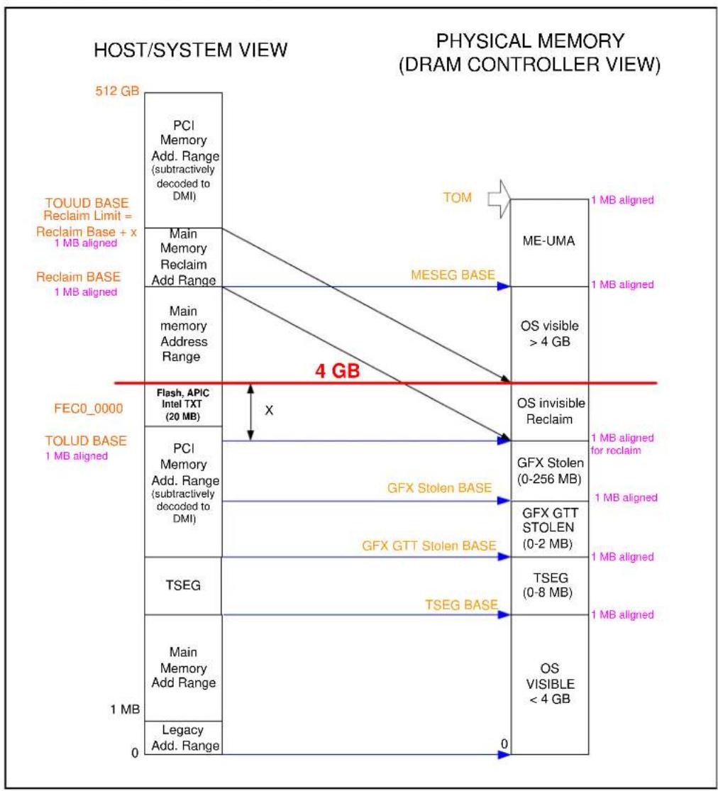
Figure 2-1 represents system memory address map in a simplified form.
Figure 2-1. System Address Range Example
flowchart
graph TD
    A["TOUD BASE Reclaim Limit = Reclaim Base + x 1 MB aligned"] --> B["PCI Memory Add. Range (subtractively decoded to DMI)"]
    C["Reclaim BASE 1 MB aligned"] --> D["Main Memory Reclaim Add Range"]
    E["FEC0_0000"] --> F["Flash, APIC Intel TXT (20 MB)"]
    F --> G["PCI Memory Add. Range (subtractively decoded to DMI)"]
    G --> H["GFX Stolen BASE"]
    H --> I["GFX GTT Stolen BASE"]
    I --> J["TSEG"]
    J --> K["TSEG BASE"]
    K --> L["OS VISIBLE < 4 GB"]
    M["TOUID BASE"] --> N["Main memory Address Range"]
    N --> O["ME-UMA"]
    O --> P["OS visible > 4 GB"]
    Q["TOUID BASE"] --> R["Main memory Add Range"]
    R --> S["OS invisible Reclaim"]
    T["TOUID BASE"] --> U["Main memory Add Range"]
    U --> V["GFX Stolen (0-256 MB)"]
    V --> W["GFX GTT STOLEN (0-2 MB)"]
    W --> X["TSEG (0-8 MB)"]
    X --> Y["OS VISIBLE < 4 GB"]
    Z["TOUID BASE"] --> AA["Main memory Add Range"]
    AA --> AB["Legacy Add. Range"]
    AC["TOUID BASE"] --> AD["Main memory Address Range"]
    AD --> AE["OS visible > 4 GB"]
    AF["TOUID BASE"] --> AG["Main memory Add Range"]
    AG --> AH["GFX Stolen BASE"]
    AH --> AI["GFX GTT STOLEN (0-2 MB)"]
    AI --> AJ["TSEG (0-8 MB)"]
    AJ --> AK["OS VISIBLE < 4 GB"]
    AL["TOUID BASE"] --> AM["Main memory Add Range"]
    AM --> AN["GFX Stolen BASE"]
    AN --> AO["GFX GTT STOLEN (0-2 MB)"]
    AO --> AP["TSEG (0-8 MB)"]
    AP --> AQ["OS VISIBLE < 4 GB"]
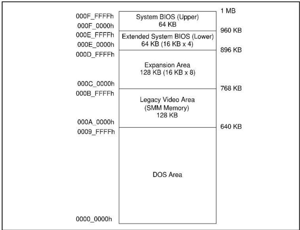
2.3.1 Legacy Address Range
This area is divided into the following address regions:
• 0–640 KB – DOS Area
• 640-768 KB - Legacy Video Buffer Area
- 768–896 KB in 16 KB sections (total of 8 sections) – Expansion Area
- 896–960 KB in 16 KB sections (total of 4 sections) – Extended System BIOS Area
• 960 KB-1 MB Memory – System BIOS Area
Figure 2-2. DOS Legacy Address Range
bar_stacked
| Category | Memory Type | Value (MB) | | :--- | :--- | :--- | | 000F_FFFFh | System BIOS (Upper) | 1 | | 000F_0000h | 64 KB | 960 KB | | 000E_FFFFh | Extended System BIOS (Lower) | 896 KB | | 000E_0000h | 64 KB (16 KB x 4) | 896 KB | | 000D_FFFFh | Expansion Area | 768 KB | | 000C_0000h | 128 KB (16 KB x 8) | 768 KB | | 000B_FFFFh | Legacy Video Area (SMM Memory) | 640 KB | | 000A_0000h | 128 KB | 640 KB | | 0009_FFFFh | DOS Area | 640 KB | | 0000_0000h | | | The chart displays a single bar representing the total memory usage of the system. The values are labeled on each bar. The first bar is labeled '1 MB', and the second bar is labeled '960 KB'.2.3.1.1 DOS Range (0h-9\_FFFFh)
The DOS area is 640 KB (0000_0000h-0009_FFFFh) in size and is always mapped to the main memory controlled by the MCH.
2.3.1.2 Legacy Video Area (A\_0000h-B\_FFFFh)
The legacy 128 KB VGA memory range, frame buffer, (000A_0000h-000B_FFFFh) can be mapped to IGD (Device 2), to PCI Express (Device 1 or Device 6), and/or to the DMI Interface. The appropriate mapping depends on which devices are enabled and the programming of the VGA steering bits. Based on the VGA steering bits, priority for VGA mapping is constant. The processor always decodes internally mapped devices first.
Non-SMM-mode processor accesses to this range are considered to be to the Video Buffer Area as described above.
The processor always positively decodes internally mapped devices, namely the IGD and PCI-Express. Subsequent decoding of regions mapped to PCI Express or the DMI Interface depends on the Legacy VGA configuration bits (VGA Enable and MDAP). This region is also the default for SMM space.
Compatible SMRAM Address Range (A\_0000h-B\_FFFFh)
When compatible SMM space is enabled, SMM-mode processor accesses to this range route to physical system DRAM at 000A_0000h-000B_FFFFh.
PCI Express and DMI originated cycles to enable SMM space are not allowed and are considered to be to the Video Buffer Area, if IGD is not enabled as the VGA device. DMI initiated write cycles are attempted as peer write cycles to a VGA enabled PCIe port.
Monochrome Adapter (MDA) Range (B\_0000h-B\_7FFFh)
Legacy support requires the ability to have a second graphics controller (monochrome) in the system. Accesses in the standard VGA range are forwarded to IGD, PCI-Express, or the DMI Interface (depending on configuration bits). Since the monochrome adapter may be mapped to any of these devices, the processor must decode cycles in the MDA range (000B_0000h-000B_7FFFh) and forward either to IGD, PCI-Express, or the DMI Interface. This capability is controlled by the VGA steering bits and the legacy configuration bit (MDAP bit). In addition to the memory range B0000h to B7FFFh, the processor decodes I/O cycles at 3B4h, 3B5h, 3B8h, 3B9h, 3BAh, and 3BFh and forwards them to either IGD, PCI-Express, and/or the DMI Interface.
PEG 16-bit VGA Decode
In the PCI to PCI Bridge Architecture Specification, Revision 1.2 it is required that 16-bit VGA decode be a feature.
When 16-bit VGA decode is disabled, the decode of VGA I/O addresses is performed on 10 lower bits only, essentially mapping also the aliases of the defined I/O addresses.
2.3.1.3 PAM (C\_0000h-F\_FFFFh)
The 13 sections from 768 KB to 1 MB comprise what is also known as the PAM Memory Area. Each section has Read enable and Write enable attributes.
The PAM registers are mapped in Device 0 configuration space.
• ISA Expansion Area (C_0000h-D_FFFFh)
- Extended System BIOS Area (E_0000h-E_FFFFh)
- System BIOS Area (F_0000h-F_FFFFh)
The processor decodes the Core request, then routes to the appropriate destination (DRAM or DMI).
Snooped accesses from PCI Express or DMI to this region are snooped on processor caches.
Non-snooped accesses from PCI Express or DMI to this region are always sent to DRAM.
Graphics translated requests to this region are not allowed. If such a mapping error occurs, the request will be routed to C_0000h. Writes will have the byte enables de-asserted.
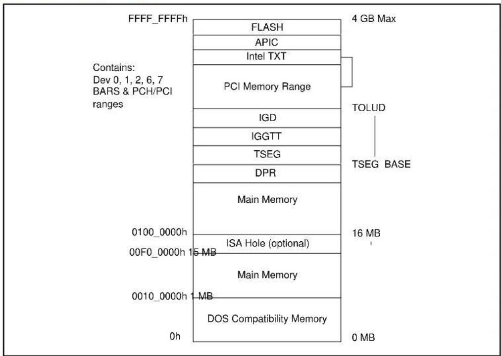
2.3.2 Main Memory Address Range (1 MB - TOLUD)
This address range extends from 1 MB to the top of Low Usable physical memory that is permitted to be accessible by the processor (as programmed in the TOLUD register). The processor will route all addresses within this range to the DRAM unless it falls into the optional TSEG, or optional ISA Hole, or optional IGD stolen VGA memory.
Figure 2-3. Main Memory Address Range
The ISA Hole is enabled in the Legacy Access Control Register in Device 0 configuration space. If no hole is created, the processor will route the request to DRAM. If a hole is created, the processor will route the request to DMI, since the request does not target DRAM.
Graphics translated requests to the range will always route to DRAM.
2.3.2.2 TSEG
For processor initiated transactions, the processor rely on correct programming of SMM Range Registers (SMRR) to enforce TSEG protection.
TSEG is below IGD stolen memory, which is at the Top of Low Usable physical memory (TOLUD). BIOS will calculate and program the TSEG BASE in Device 0 (TSEGMB), used protect this region from DMA access. The calculation is:
$$ \text { TSEGMB } = \text { TOLUD } - \text { DSM SIZE } - \text { GSM SIZE } - \text { TSEG SIZE } $$
SMM-mode processor accesses to enabled TSEG access the physical DRAM at the same address.
When the extended SMRAM space is enabled, processor accesses to the TSEG range without SMM attribute or without WB attribute are handled by the processor as invalid accesses.
Non-processor originated accesses are not allowed to SMM space. PCI-Express, DMI, and Internal Graphics originated cycle to enabled SMM space are handled as invalid cycle type with reads and writes to location C_0000h and byte enables turned off for writes.
2.3.2.3 Protected Memory Range (PMR) – (programmable)
For robust and secure launch of the MVMM, the MVMM code and private data needs to be loaded to a memory region protected from bus master accesses. Support for protected memory region is required for DMA-remapping hardware implementations on platforms supporting Intel TXT, and is optional for non-Intel TXT platforms. Since the protected memory region needs to be enabled before the MVMM is launched, hardware must support enabling of the protected memory region independently from enabling the DMA-remapping hardware.
As part of the secure launch process, the SINIT-AC module verifies the protected memory regions are properly configured and enabled. Once launched, the MVMM can setup the initial DMA-remapping structures in protected memory (to ensure they are protected while being setup) before enabling the DMA-remapping hardware units.
To optimally support platform configurations supporting varying amounts of main memory, the protected memory region is defined as two non-overlapping regions:
- Protected Low-memory Region – This is defined as the protected memory region below 4 GB to hold the MVMM code/private data, and the initial DMA-remapping structures that control DMA to host physical addresses below 4 GB. DMA-remapping hardware implementations on platforms supporting Intel TXT are required to support protected low-memory region 5.
- Protected High-memory Region – This is defined as a variable sized protected memory region above 4 GB, enough to hold the initial DMA-remapping structures
for managing DMA accesses to addresses above 4 GB. DMA-remapping hardware implementations on platforms supporting Intel TXT are required to support protected high-memory region6, if the platform supports main memory above 4 GB.
Once the protected low/high memory region registers are configured, bus master protection to these regions is enabled through the Protected Memory Enable register. For platforms with multiple DMA-remapping hardware units, each of the DMA-remapping hardware units must be configured with the same protected memory regions and enabled.
2.3.2.4 DRAM Protected Range (DPR)
This protection range only applies to DMA accesses and GMADR translations. It serves a purpose of providing a memory range that is only accessible to processor streams.
The DPR range works independent of any other range, including the PMRC checks in VT-d. It occurs post any VT-d translation. Therefore, incoming cycles are checked against this range after the VT-d translation and faulted if they hit this protected range, even if they passed the VT-d translation.
The system will set up:
- 0 to (TSEG_BASE - DPR size - 1) for DMA traffic
- TSEG_BASE to (TSEG_BASE - DPR size) as no DMA.
After some time, software could request more space for not allowing DMA. It will get some more pages and make sure there are no DMA cycles to the new region. DPR size is changed to the new value. When it does this, there should not be any DMA cycles going to DRAM to the new region.
If there were cycles from a rogue device to the new region, then those could use the previous decode until the new decode can guarantee PV. No flushing of cycles is required. On a clock by clock basis proper decode with the previous or new decode needs to be ensured.
All upstream cycles from 0 to (TSEG_BASE - 1 - DPR size), and not in the legacy holes (VGA), are decoded to DRAM.
Because Bus Master cycles can occur when the DPR size is changed, the DPR size needs to be treated dynamically.
2.3.2.5 Pre-allocated Memory
Voids of physical addresses that are not accessible as general system memory and reside within system memory address range (< TOLUD) are created for SMM-mode, legacy VGA graphics compatibility, and GFX GTT stolen memory. It is the responsibility of BIOS to properly initialize these regions.
2.3.2.6 GFX Stolen Spaces
2.3.2.6.1 GTT Stolen Space (GSM)
GSM is allocated to store the GFX translation table entries.
GSM always exists regardless of VT-d as long as internal GFX is enabled. This space is allocated to store accesses as page table entries are getting updated through virtual GTTMMADR range. Hardware is responsible to map PTEs into this physical space.
Direct accesses to GSM are not allowed, only hardware translations and fetches can be directed to GSM.
2.3.2.7 ME UMA
ME (the iAMT Manageability Engine) can be allocated UMA memory. ME memory is "stolen" from the top of the Host address map. The ME stolen memory base is calculated by subtracting the amount of memory stolen by the Manageability Engine from TOM.
Only ME can access this space; it is not accessible by or coherent with any processor side accesses.
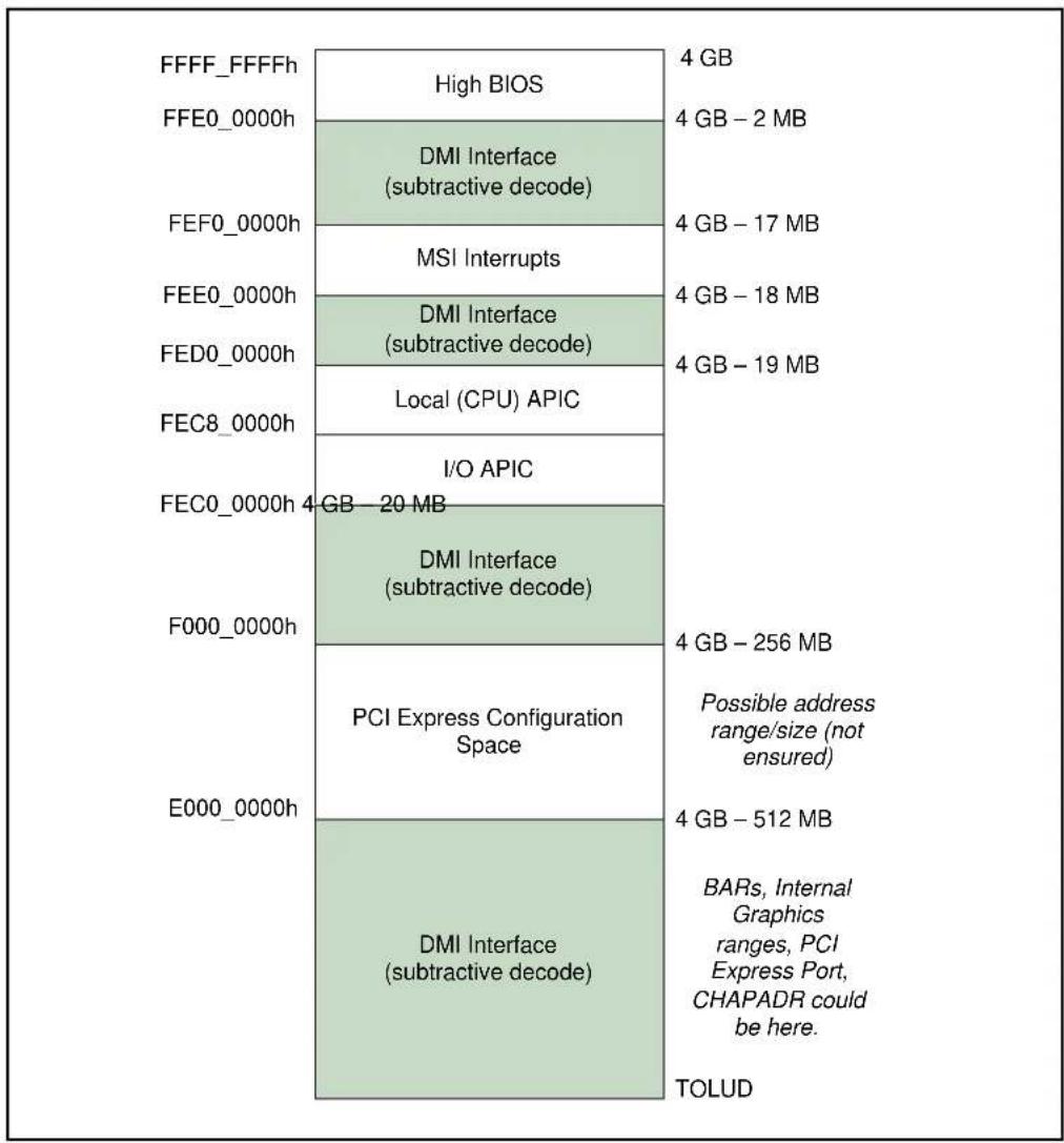
2.3.3 PCI Memory Address Range (TOLUD - 4 GB)
This address range, from the top of low usable DRAM (TOLUD) to 4 GB is normally mapped to the DMI Interface.
Device 0 exceptions are:
- Addresses decoded to the egress port registers (PXPEPBAR)
- Addresses decoded to the memory mapped range for internal MCH registers (MCHBAR)
- Addresses decoded to the registers associated with the MCH/ICH Serial Interconnect (DMI) register memory range. (DMIBAR)
For each PCI Express port, there are two exceptions to this rule:
- Addresses decoded to the PCI Express Memory Window defined by the MBASE, MLIMIT, registers are mapped to PCI Express.
- Addresses decoded to the PCI Express prefetchable Memory Window defined by the PMBASE, PMLIMIT, registers are mapped to PCI Express.
In integrated graphics configurations, there are exceptions to this rule:
- Addresses decode to the internal graphics translation window (GMADR)
- Addresses decode to the Internal graphics translation table or IGD registers. (GTTMMADR)
In a VT enable configuration, there are exceptions to this rule:
- Addresses decoded to the memory mapped window to PEG/DMI VC0 VT remap engine registers (VTDPVC0BAR)
- Addresses decoded to the memory mapped window to Graphics VT remap engine registers (GFXVTBAR)
- TCm accesses (to ME stolen memory) from PCH do not go through VT remap engines.
Some of the MMIO Bars may be mapped to this range or to the range above TOUUD.
There are sub-ranges within the PCI Memory address range defined as APIC Configuration Space, MSI Interrupt Space, and High BIOS Address Range. The exceptions listed above for internal graphics and the PCI Express ports MUST NOT overlap with these ranges.
Figure 2-4. PCI Memory Address Range
bar_stacked
| Category | Component | Value | | :--- | :--- | :--- | | FFFF_FFFFh | High BIOS | 4 GB | | FFE0_0000h | DMI Interface (subtractive decode) | 4 GB - 2 MB | | FEF0_0000h | MSI Interrupts | 4 GB - 17 MB | | FEE0_0000h | DMI Interface (subtractive decode) | 4 GB - 18 MB | | FED0_0000h | Local (CPU) APIC | 4 GB - 19 MB | | FEC8_0000h | I/O APIC | | | FEC0_0000h 4GB - 20 MB | DMI Interface (subtractive decode) | | | F000_0000h | PCI Express Configuration Space | 4 GB - 256 MB Possible address range/size (not ensured) | | E000_0000h | DMI Interface (subtractive decode) | 4 GB - 512 MB BARs, Internal Graphics ranges, PCI Express Port, CHAPADR could be here. TOLUD |2.3.3.1 APIC Configuration Space (FEC0\_0000h-FECF\_FFFFh)
This range is reserved for APIC configuration space. The I/O APIC(s) usually reside in the PCH portion of the chip-set, but may also exist as stand-alone components like PXH.
The IOAPIC spaces are used to communicate with IOAPIC interrupt controllers that may be populated in the system. Since it is difficult to relocate an interrupt controller using plug-and-play software, fixed address decode regions have been allocated for them. Processor accesses to the default IOAPIC region (FEC0_0000h to FEC7_FFFFh) are always forwarded to DMI.
The processor optionally supports additional I/O APICs behind the PCI Express "Graphics" port. When enabled using the APIC_BASE and APIC_LIMIT registers (mapped PCI Express Configuration space offset 240h and 244h), the PCI Express port(s) will positively decode a subset of the APIC configuration space.
Memory requests to this range would then be forwarded to the PCI Express port. This mode is intended for the entry Workstation/Server SKUs of the processor, and would be disabled in typical Desktop systems. When disabled, any access within entire APIC Configuration space (FEC0_0000h to FECF_FFFFh) is forwarded to DMI.
2.3.3.2 HSEG (FEDA\_0000h-FEDB\_FFFFh)
This decode range is not supported on the Intel ^® Xeon ^® processor E3-1200 family platform.
2.3.3.3 MSI Interrupt Memory Space (FEE0\_0000h-FEEF\_FFFFh)
Any PCI Express or DMI device may issue a Memory Write to 0FEEx_xxxxh. This Memory Write cycle does not go to DRAM. The system agent will forward this Memory Write along with the data to the processor as an Interrupt Message Transaction.
2.3.3.4 High BIOS Area
For security reasons, the processor will positively decode this range to DMI. This positive decode will ensure any overlapping ranges will be ignored.
The top 2 MB (FFE0_0000h-FFFF_FFFFh) of the PCI Memory Address Range is reserved for System BIOS (High BIOS), extended BIOS for PCI devices, and the A20 alias of the system BIOS. The processor begins execution from the High BIOS after reset. This region is positively decoded to DMI. The actual address space required for the BIOS is less than 2 MB but the minimum processor MTRR range for this region is 2 MB so that full 2 MB must be considered.
2.3.4 Main Memory Address Space (4 GB to TOUUD)
The processor supports 39-bit addressing.
The maximum main memory size supported is 32 GB total DRAM memory. A hole between TOLUD and 4 GB occurs when main memory size approaches 4 GB or larger. As a result, TOM, and TOUUD registers and REMAPBASE/REMAPLIMIT registers become relevant.
The remap configuration registers exist to remap lost main memory space. The greater than 32-bit remap handling will be handled similar to other MCHs.
Upstream read and write accesses above 39-bit addressing are treated as invalid cycles by PEG and DMI.
Top of Memory (TOM)
The "Top of Memory" (TOM) register reflects the total amount of populated physical memory. This is NOT necessarily the highest main memory address (holes may exist in main memory address map due to addresses allocated for memory mapped IO above TOM).
On FSB chipsets, the TOM was used to allocate the Manageability Engine's stolen memory. The Manageability Engine's (ME) stolen size register reflects the total amount of physical memory stolen by the Manageability Engine. The ME stolen memory is located at the top of physical memory. The ME stolen memory base is calculated by subtracting the amount of memory stolen by the Manageability Engine from TOM.
Top of Upper Usable DRAM (TOUUD)
The Top of Upper Usable Dram (TOUUD) register reflects the total amount of addressable DRAM. If remap is disabled, TOUUD will reflect TOM minus Manageability Engine's stolen size. If remap is enabled, then it will reflect the remap limit. Note, when there is more than 4 GB of DRAM and reclaim is enabled, the reclaim base will be the same as TOM minus ME stolen memory size to the nearest 1 MB alignment (shown in case 2 below).
Top of Low Usable DRAM (TOLUD)
TOLUD register is restricted to 4 GB memory (A[31:20]), but the processor can support up to 32 GB, limited by DRAM pins. For physical memory greater than 4 GB, the TOUUD register helps identify the address range between the 4 GB boundary and the top of physical memory. This identifies memory that can be directly accessed (including remap address calculation), which is useful for memory access indication and early path indication. TOLUD can be 1 MB aligned.
TSEG\_BASE
The "TSEG_BASE" register reflects the total amount of low addressable DRAM, below TOLUD. BIOS will calculate and program this register, so the system agent has knowledge of where (TOLUD)-(Gfx stolen)-(Gfx GTT stolen)-(TSEG) is located. I/O blocks use this minus DPR for upstream DRAM decode.
2.3.4.1 Memory Re-claim Background
The following are examples of Memory Mapped IO devices that are typically located below 4 GB:
- High BIOS
• TSEG - GFX stolen
- GTT stolen
• XAPIC - Local APIC
- MSI Interrupts
- Mbase/Mlimit
- Pmbase/PMlimit
- Memory Mapped IO space that supports only 32B addressing
The processor provides the capability to re-claim the physical memory overlapped by the Memory Mapped IO logical address space. The processor re-maps physical memory from the Top of Low Memory (TOLUD) boundary up to the 4 GB boundary to an equivalent sized logical address range located just below the Manageability Engine's stolen memory.
2.3.4.2 Indirect Accesses to MCHBAR Registers
This access is similar to prior chipsets. MCHBAR registers can be indirectly accessed using:
- Direct MCHBAR access decode
- Cycle to memory from processor
- Hits MCHBAR base, AND
- MCHBAR is enabled, AND
- Within MMIO space (above and below 4 GB)
- GTTMMADR (10000h-13FFFh) range -> MCHBAR decode
- Cycle to memory from processor, AND
- Device 2 (IGD) is enabled, AND
- Memory accesses for device 2 is enabled, AND
- Targets GFX MMIO Function 0, AND
- MCHBAR is enabled or cycle is a read. If MCHBAR is disabled, only read access is allowed.
- MCHTMBAR -> MCHBAR (Thermal Monitor)
-
Cycle to memory from processor, AND
-
AND Targets MCHTMBAR base
- IOBAR -> GTTMMADR -> MCHBAR. Follows IOBAR rules. See GTTMMADR information above as well.
2.3.4.3 Memory Remapping
An incoming address (referred to as a logical address) is checked to see if it falls in the memory re-map window. The bottom of the re-map window is defined by the value in the REMAPBASE register. The top of the re-map window is defined by the value in the REMAPLIMIT register. An address that falls within this window is remapped to the physical memory starting at the address defined by the TOLUD register. The TOLUD register must be 1 MB aligned.
2.3.4.4 Hardware Remap Algorithm
The following pseudo-code defines the algorithm used to calculate the DRAM address to be used for a logical address above the top of physical memory made available using re-claiming.
IF (ADDRESS_IN[38:20] REMAP_BASE[35:20]) AND
(ADDRESS_IN[38:20] REMAP_LIMIT[35:20]) THEN
ADDRESS_OUT[38:20] = (ADDRESS_IN[38:20] - REMAP_BASE[35:20]) + 0000000b and TOLUD[31:20]
ADDRESS_OUT[19:0] = ADDRESS_IN[19:0]
2.3.4.5 Programming Model
The memory boundaries of interest are:
- Bottom of Logical Address Remap Window defined by the REMAPBASE register, which is calculated and loaded by BIOS.
- Top of Logical Address Remap Window defined by the REMAPLIMIT register, which is calculated and loaded by BIOS.
- Bottom of Physical Remap Memory defined by the existing TOLUD register.
- Top of Physical Remap Memory, which is implicitly defined by either 4 GB or TOM minus Manageability Engine stolen size.
Mapping steps:
- Determine TOM
- Determine TOM minus ME stolen size
- Determine MMIO allocation
- Determine TOLUD
- Determine GFX stolen base
- Determine GFX GTT stolen base
- Determine TSEG base
- Determine remap base/limit
- Determine TOUUD
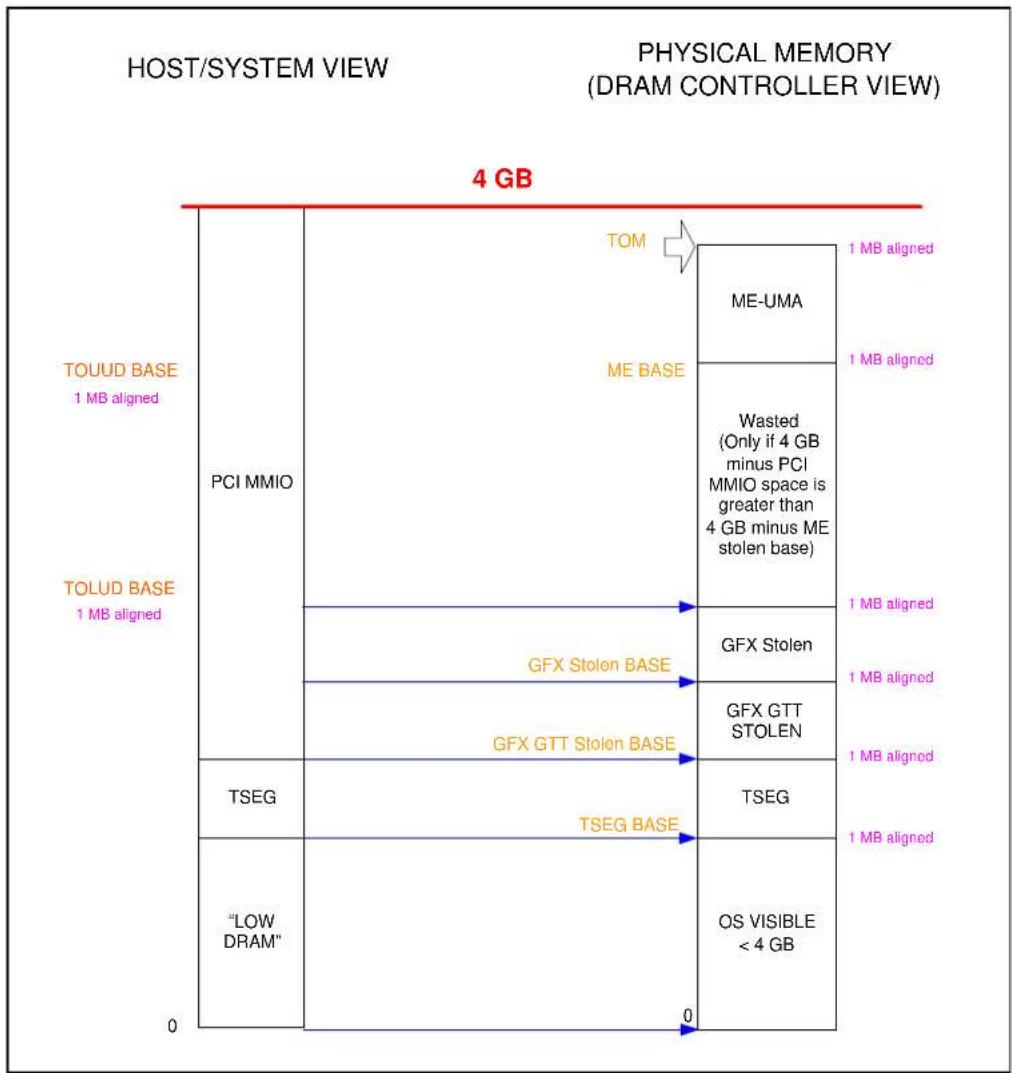
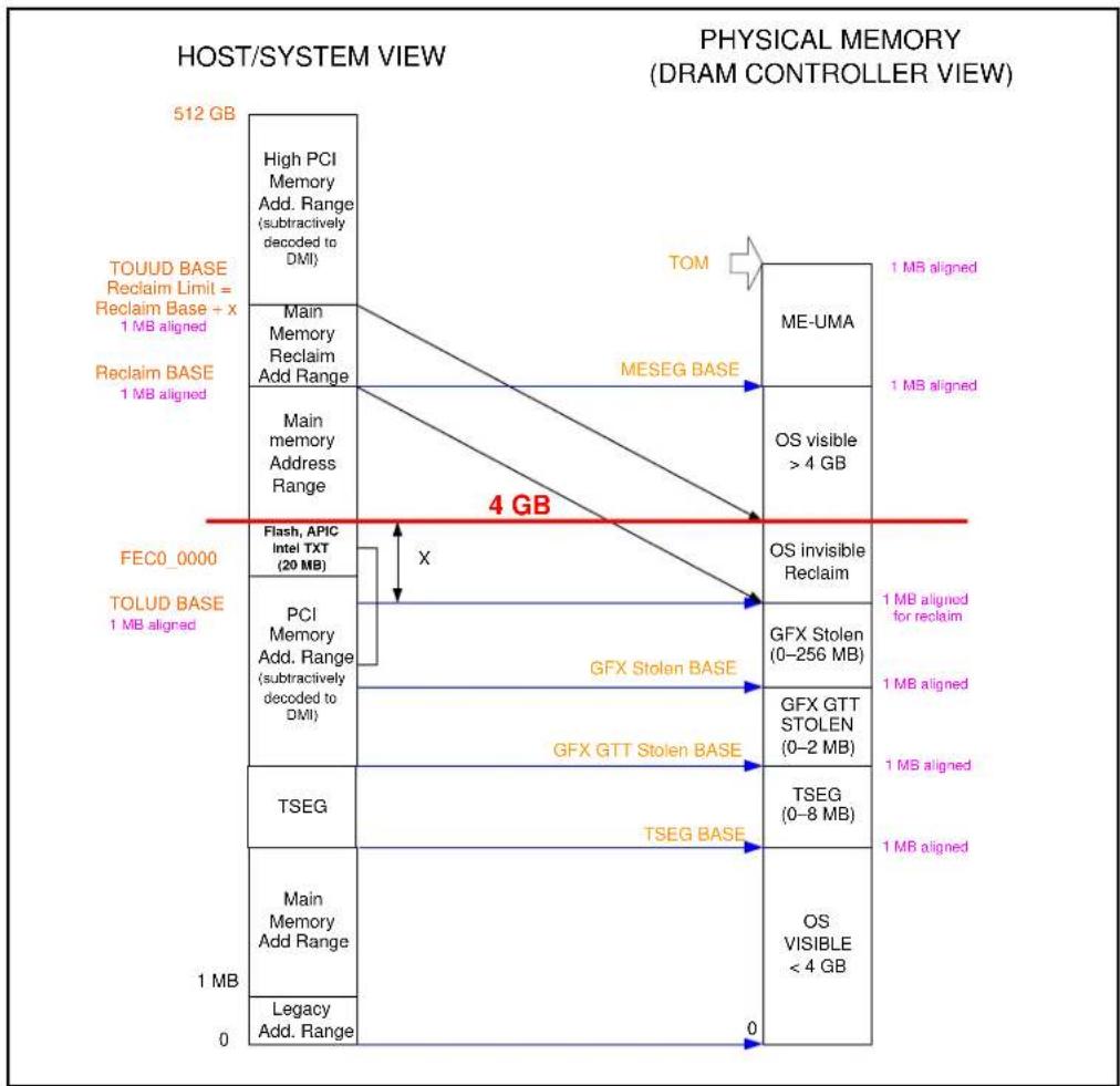
Figure 2-5 and Figure 2-6 show the two possible general cases of remapping.
Case 1 – Less than 4 GB of Physical Memory (no remap)
Figure 2-5. Case 1 – Less than 4 GB of Physical Memory (no remap)
bar_stacked
| Memory Type | Component | Value | | ----------------- | ----------------- | --------- | | TOUUD BASE | PCI MMIO | 1 MB aligned | | TOUUD BASE | ME BASE | 1 MB aligned | | TOUUD BASE | Wasted (Only if 4 GB minus PCI MMIO space is greater than 4 GB minus ME stolen base) | 1 MB aligned | | TOUUD BASE | GFX Stolen BASE | 1 MB aligned | | TOUUD BASE | GFX GTT Stolen BASE| 1 MB aligned | | TOUUD BASE | TSEG | 1 MB aligned | | TOUUD BASE | TSEG BASE | 1 MB aligned | | TOLUD BASE | "LOW DRAM" | 0 | | TOLUD BASE | OS VISIBLE < 4 GB | 0 |- Populated Physical Memory = 2 GB
- Address Space allocated to memory mapped IO = 1 GB
- Remapped Physical Memory = 0 GB
• TOM - 00_7FF0_0000h (2 GB)
- ME base - 00_7FF0_0000h (1 MB)
• ME Mask - 00_7FF0_0000h
- TOUUD - 00_0000_0000h (Disable - Avoid access above 4 GB)
• TOLUD - 00_7FE0_0000h (2 GB minus 1 MB)
- REMAPBASE - 7F_FFFF_0000h (default)
- REMAPLIMIT - 00_0000_0000h (0 GB boundary, default)
Case 2 - Greater than 4 GB of Physical Memory
Figure 2-6. Case 2 – Greater than 4 GB of Physical Memory
flowchart
graph TD
    A["512 GB"] --> B["High PCI Memory Add. Range (subtractively decoded to DMI)"]
    B --> C["Main Memory Reclaim Add Range"]
    C --> D["Main memory Address Range"]
    D --> E["TOM"]
    E --> F["ME-UMA"]
    F --> G["OS visible > 4 GB"]
    G --> H["OS invisible Reclaim"]
    H --> I["GFX Stolen (0–256 MB)"]
    I --> J["GFX GTT STOLEN (0–2 MB)"]
    J --> K["TSEG (0–8 MB)"]
    K --> L["OS VISIBLE < 4 GB"]
    L --> M["Legacy Add. Range"]
    M --> N["1 MB"]
    style A fill:#f9f,stroke:#333
    style B fill:#ccf,stroke:#333
    style C fill:#cfc,stroke:#333
    style D fill:#fcc,stroke:#333
    style E fill:#ffc,stroke:#333
    style F fill:#cff,stroke:#333
    style G fill:#ffc,stroke:#333
    style H fill:#ffc,stroke:#333
    style I fill:#ffc,stroke:#333
    style J fill:#ffc,stroke:#333
    style K fill:#ffc,stroke:#333
    style L fill:#ffc,stroke:#333
    style M fill:#ffc,stroke:#333
    style N fill:#ffc,stroke:#333
In this case the amount of memory remapped is the range between TOLUD and 4 GB. This physical memory will be mapped to the logical address range defined between the REMAPBASE and the REMAPLIMIT registers.
Example: 5 GB of Physical Memory, with 1 GB allocated to Memory Mapped IO:
- Populated Physical Memory = 5 GB
- Address Space allocated to memory mapped IO (including Flash, APIC, and Intel TXT) = 1 GB
- Remapped Physical Memory = 1 GB
• TOM - 01_4000_0000h (5 GB)
• ME stolen size - 00000b (0 MB)
• TOUUD - 01_8000_0000h (6 GB) (1 MB aligned)
• TOLUD - 00_C000_000h (3 GB) - REMAPBASE - 01_4000_0000h (5 GB)
- REMAPLIMIT - 01_7FF0_0000h (6 GB-1)
The Remap window is inclusive of the Base and Limit addresses. In the decoder A[19:0] of the Remap Base Address are assumed to be 0s. Similarly, A[19:0] of the Remap Limit Address are assumed to be Fhs. Thus, the bottom of the defined memory range will be aligned to a megabyte boundary and the top of the defined range will be one less than a MB boundary.
Setting the Remap Base register to a value greater than that programmed into the Remap Limit register disables the remap function.
Software Responsibility and Restrictions
- BIOS is responsible for programming the REMAPBASE and REMAPLIMIT registers based on the values in the TOLUD, TOM, and ME stolen size registers.
- The amount of remapped memory defined by the REMAPBASE and REMAPLIMIT registers must be equal to the amount of physical memory between the TOLUD and the lower of either 4 GB or TOM minus the ME stolen size.
- Addresses of MMIO region must not overlap with any part of the Logical Address Memory Remap range.
- When TOM is equal to TOLUD, remap is not needed and must be disabled by programming REMAPBASE to a value greater than the value in the REMAPLIMIT register.
Interaction with other Overlapping Address Space
The following Memory Mapped IO address spaces are all logically addressed below 4 GB where they do not overlap the logical address of the re-mapped memory region:
GFXGTTstolen At (TOLUD - GFXstolensize) to TOLUD
GFXstolen At ((TOLUD - GFXstolensize) - GFXGTTstolensize) to (TOLUD - GFXstolensize)
TSEG At ((TOLUD - GFXstolensize - GFXGTTstolensize) - TSEGSIZE) to (TOLUD - GFXGTTstolensize - GFXstolensize)
High BIOS Reset vector just under 4GB boundary (Positive decode to DMI occurs)
XAPIC At fixed address below 4 GB
Local APIC At fixed address below 4 GB
MSI Interrupts At fixed address below 4 GB
GMADR 64 bit BARs
GTTMMADR 64 bit BARs MBASE/MLIMIT
PXPEPBAR 39 bit BAR
DMIBAR 39 bit BAR
MCHBAR 39 bit BAR
TMBAR 64 bit BAR
PMBASE/PMLIMIT 64 bit BAR (using Upper PMBASE/PMLIMIT)
CHAPADR 64 bit BAR
GFXVTBAR 39 bit BARs
VTDPVC0BAR 39 bit BARs
Implementation Notes
- Remap applies to transactions from all interfaces. All upstream PEG/DMI transactions that are snooped get remapped.
- Upstream PEG/DMI transactions that are not snooped ("Snoop not required" attribute set) get remapped.
- Upstream reads and writes above TOUUD are treated as invalid cycles.
- Remapped addresses remap starting at TOLUD. They do not remap starting at TSEG_BASE. DMI and PEG need to be careful with this for both snoop and non-snoop accesses. In other words, for upstream accesses, the range between (TOLUD – GfxStolensize-GFXGTTstolensize – TSEGSIZE-DPR) to TOLUD) will never map directly to memory.
Note: Accesses from PEG/DMI should be decoded as to the type of access before they are remapped. For instance a DMI write to FEEx_xxxx is an interrupt transaction, but there is a DMI address that will be re-mapped to the DRAM address of FEEx_xxxx. In all cases, the remapping of the address is done only after all other decodes have taken place.
Unmapped Addresses between TOLUD and 4 GB
Accesses that do not hit DRAM or PCI space are subtractive decoded to DMI. Because the TOLUD register is used to mark the upper limit of DRAM space below the 4 GB boundary, no address between TOLUD and 4 GB ever decodes directly to main memory. Thus, even if remap is disabled, any address in this range has a non-memory destination.
The top of DRAM address space is either:
• TOLUD if there is less then 4 GB of DRAM or 32-bit addressing or
• TOUUD if there is more than 4 GB of DRAM and 36-bit addressing.
Note: The system address space includes the remapped range. For instance, if there is 8 GB of DRAM and 1 GB of PCI space, the system has a 9 GB address space, where DRAM lies from 0-3 GB and 4-9 GB. BIOS will report an address space of 9 GB to the OS.
2.3.5 PCI Express\* Configuration Address Space
Unlike previous platforms, PCIEXBAR is located in device 0 configuration space as in FSB platforms. The processor detects memory accesses targeting PCIEXBAR. BIOS must assign this address range such that it will not conflict with any other address ranges.
See the configuration portion of this document for more details.
2.3.6 PCI Express\* Graphics Attach (PEG)
The processor can be programmed to direct memory accesses to a PCI Express interface. When addresses are within either of two ranges specified using registers in each PEG(s) configuration space.
- The first range is controlled using the Memory Base Register (MBASE) and Memory Limit Register (MLIMIT) registers.
- The second range is controlled using the Pre-fetchable Memory Base (PMBASE) and Pre-fetchable Memory Limit (PMLIMIT) registers.
Conceptually, address decoding for each range follows the same basic concept. The top 12 bits of the respective Memory Base and Memory Limit registers correspond to address bits A[31:20] of a memory address. For the purpose of address decoding, the processor assumes that address bits A[19:0] of the memory base are zero and that address bits A[19:0] of the memory limit address are F_FFFFh. This forces each memory address range to be aligned to 1 MB boundary and to have a size granularity of 1 MB.
The processor positively decodes memory accesses to PCI Express memory address space as defined by the following equations:
Memory_Base_Address Address Memory_Limit_Address
Prefetchable_Memory_Base_Address Address ≤ Prefetchable_Memory_Limit_Address
The window size is programmed by the plug-and-play configuration software. The window size depends on the size of memory claimed by the PCI Express device. Normally these ranges will reside above the Top-of-Low Usable-DRAM and below High BIOS and APIC address ranges. They MUST reside above the top of low memory (TOLUD) if they reside below 4 GB and MUST reside above top of upper memory (TOUUD) if they reside above 4 GB or they will steal physical DRAM memory space.
It is essential to support a separate Pre-fetchable range in order to apply USWC attribute (from the processor point of view) to that range. The USWC attribute is used by the processor for write combining.
Note that the processor memory range registers described above are used to allocate memory address space for any PCI Express devices sitting on PCI Express that require such a window.
The PCICMD register can override the routing of memory accesses to PCI Express. In other words, the memory access enable bit must be set to enable the memory base/limit and pre-fetchable base/limit windows.
The upper PMUBASE/PMULIMIT registers are implemented for PCI Express Specification compliance. The processor locates MMIO space above 4 GB using these registers.
2.3.7 Graphics Memory Address Ranges
The MCH can be programmed to direct memory accesses to IGD when addresses are within any of five ranges specified using registers in the processor Device 2 configuration space.
- The Graphics Memory Aperture Base Register (GMADR) is used to access graphics memory allocated using the graphics translation table.
- The Graphics Translation Table Base Register (GTTADR) is used to access the translation table and graphics control registers. This is part of GTTMMADR register.
These ranges can reside above the Top-of-Low-DRAM and below High BIOS and APIC address ranges. They MUST reside above the top of memory (TOLUD) and below 4 GB so they do not steal any physical DRAM memory space.
Alternatively, these ranges can reside above 4 GB, similar to other BARs which are larger than 32 bits in size.
GMADR is a Prefetchable range in order to apply USWC attribute (from the processor point of view) to that range. The USWC attribute is used by the processor for write combining.
2.3.7.1 IOBAR Mapped Access to Device 2 MMIO Space
Device 2, integrated graphics device, contains an IOBAR register. If Device 2 is enabled, then IGD registers or the GTT table can be accessed using this IOBAR. The IOBAR is composed of an index register and a data register.
MMIO_Index - MMIO_INDEX is a 32-bit register. A 32-bit (all bytes enabled) I/O write to this port loads the offset of the MMIO register or offset into the GTT that needs to be accessed. An I/O Read returns the current value of this register. An I/O read/write accesses less than 32 bits in size (all bytes enabled) will not target this register.
MMIO_Data - MMIO_DATA is a 32-bit register. A 32-bit (all bytes enabled) I/O write to this port is re-directed to the MMIO register pointed to by the MMIO-index register. An I/O read to this port is re-directed to the MMIO register pointed to by the MMIO-index register. An I/O read/write accesses less than 32 bits in size (all bytes enabled) will not target this register.
The result of accesses through IOBAR can be:
- Accesses directed to the GTT table. (that is, route to DRAM)
- Accesses to internal graphics registers with the device.
- Accesses to internal graphics display registers now located within the PCH. (that is, route to DMI).
Note that GTT table space writes (GTTADR) are supported through this mapping mechanism.
This mechanism to access internal graphics MMIO registers must not be used to access VGA IO registers which are mapped through the MMIO space. VGA registers must be accessed directly through the dedicated VGA I/O ports.
2.3.7.2 Trusted Graphics Ranges
No trusted graphics ranges are supported.
2.3.8 System Management Mode (SMM)
Unlike FSB platforms, the Core handles all SMM mode transaction routing. Also, the platform no longer supports HSEG. The processor will never allow I/O devices access to CSEG/TSEG/HSEG ranges.
DMI Interface and PCI Express masters are not allowed to access the SMM space.
Table 2-3. SMM regions
| SMM Space Enabled Transaction Address Space DRAM Space (DRAM) | |
| Compatible (C) 000A_0000h to 000B_FFFFh 000A_0000h to 000B_FFFFh | |
| TSEG (T) (TOLUD-STOLEN-TSEG) to TOLUD-STOLEN | (TOLUD-STOLEN-TSEG) to TOLUD-STOLEN |
2.3.9 SMM and VGA Access through GTT TLB
Accesses through the Graphics Translation Table (GTT) Translation Lookaside Buffer (TLB) address translation SMM DRAM space are not allowed. Writes will be routed to Memory address 000C_0000h with byte enables de-asserted and reads will be routed to Memory address 000C_0000h. If a GTT TLB translated address hits SMM DRAM space, an error is recorded in the PGTBL_ER register.
PCI Express and DMI Interface originated accesses are never allowed to access SMM space directly or through the GTT TLB address translation. If a GTT TLB translated address hits enabled SMM DRAM space, an error is recorded in the PGTBL_ER register.
PCI Express* and DMI Interface write accesses through GMADR range will not be snooped. Only PCI Express* and DMI assesses to GMADR linear range (defined using fence registers) are supported. PCI Express and DMI Interface tileY and tileX writes to GMADR are not supported. If, when translated, the resulting physical address is to enable SMM DRAM space, the request will be remapped to address 000C_0000h with de-asserted byte enables.
PCI Express and DMI Interface read accesses to the GMADR range are not supported, therefore will have no address translation concerns. PCI Express and DMI Interface reads to GMADR will be remapped to address 000C_0000h. The read will complete with UR (unsupported request) completion status.
GTT fetches are always decoded (at fetch time) to ensure not in SMM (actually, anything above base of TSEG or 640K-1M). Thus, they will be invalid and go to address 000C_0000h, but that is not specific to PCI Express or DMI; it applies to processor or internal graphics engines.
2.3.10 ME Stolen Memory Accesses
There are only 2 ways to legally access ME stolen memory.
- PCH accesses mapped to VCm will be decoded to ensure only ME stolen memory is targeted. These VCm accesses will route non-snooped directly to DRAM. This is the means by which the ME engine (located within the PCH) is able to access the ME stolen range.
- The Display engine is allowed to access MEstolen memory as part of KVM flows. Specifically, Display initiated HHP reads (for displaying a KVM frame) and display initiated LP non-snoop writes (for display writing a KVM captured frame) to ME stolen memory are allowed.
2.3.11 I/O Address Space
The system agent generates either DMI Interface or PCI Express* bus cycles for all processor I/O accesses that it does not claim. Configuration Address Register (CONFIG_ADDRESS) and the Configuration Data Register (CONFIG_DATA) are used to generate PCI configuration space access.
The processor allows 64 KB+3 bytes to be addressed within the I/O space. Note that the upper 3 locations can be accessed only during I/O address wrap-around when address bit 16 is asserted. Address bit 16 is asserted on the processor bus whenever an I/O access is made to 4 bytes from address 0FFFDh, 0FFFEh, or 0FFFFh. Address bit 16 is also asserted when an I/O access is made to 2 bytes from address 0FFFFh.
A set of I/O accesses are consumed by the internal graphics device if it is enabled. The mechanisms for internal graphics I/O decode and the associated control is explained later.
The I/O accesses are forwarded normally to the DMI Interface bus unless they fall within the PCI Express I/O address range as defined by the mechanisms explained below. I/O writes are NOT posted. Memory writes to PCH or PCI Express are posted. The PCI Express devices have a register that can disable the routing of I/O cycles to the PCI Express device.
The processor responds to I/O cycles initiated on PCI Express or DMI with an UR status. Upstream I/O cycles and configuration cycles should never occur. If one does occur, the transaction will complete with an UR completion status.
Similar to FSB processors, I/O reads that lie within 8-byte boundaries but cross 4-byte boundaries are issued from the processor as 1 transaction. It will be broke into 2 separate transactions. I/O writes that lie within 8-byte boundaries but cross 4-byte boundaries will be split into 2 transactions by the processor.
2.3.11.1 PCI Express\* I/O Address Mapping
The processor can be programmed to direct non-memory (I/O) accesses to the PCI Express bus interface when processor initiated I/O cycle addresses are within the PCI Express I/O address range. This range is controlled using the I/O Base Address (IOBASE) and I/O Limit Address (IOLIMIT) registers in Device 1 functions 0, 1, 2 or Device 6 configuration space.
Address decoding for this range is based on the following concept. The top 4 bits of the respective I/O Base and I/O Limit registers correspond to address bits A[15:12] of an I/O address. For the purpose of address decoding, the device assumes that lower 12 address bits A[11:0] of the I/O base are zero and that address bits A[11:0] of the I/O limit address are FFFh. This forces the I/O address range alignment to 4 KB boundary and produces a size granularity of 4 KB.
The processor positively decodes I/O accesses to PCI Express I/O address space as defined by the following equation:
I/O_Base_Address <processor I/O Cycle Address 1/O_Limit_Address
The effective size of the range is programmed by the plug-and-play configuration software and it depends on the size of I/O space claimed by the PCI Express device.
The processor also forwards accesses to the Legacy VGA I/O ranges according to the settings in the PEG configuration registers BCTRL (VGA Enable) and PCICMD (IOAE), unless a second adapter (monochrome) is present on the DMI Interface/PCI (or ISA). The presence of a second graphics adapter is determined by the MDAP configuration bit. When MDAP is set, the processor will decode legacy monochrome I/O ranges and forward them to the DMI Interface. The I/O ranges decoded for the monochrome adapter are 3B4h, 3B5h, 3B8h, 3B9h, 3BAh, and 3BFh.
Note that the PEG I/O address range registers defined above are used for all I/O space allocation for any devices requiring such a window on PCI-Express.
The PCICMD register can disable the routing of I/O cycles to PCI-Express.
2.3.12 MCTP and KVM Flows
Refer to the DMI2 specification for details.
MCTP cycles are not processed within the processor. MCTP cycles are merely passed from input port to destination port based on routing ID.
2.3.13 Decode Rules and Cross-Bridge Address Mapping
2.3.13.1 DMI Interface Decode Rules
All "SNOOP semantic" PCI Express* transactions are kept coherent with processor caches.
All "Snoop not required semantic" cycles must reference the main DRAM address range. PCI Express non-snoop initiated cycles are not snooped.
The processor accepts accesses from DMI Interface to the following address ranges:
- All snoop memory read and write accesses to Main DRAM including PAM region (except stolen memory ranges, TSEG, A0000h-BFFFFh space)
- Write accesses to enabled VGA range, MBASE/MLIMIT, and PMBASE/PMLIMIT will be routed as peer cycles to the PCI Express interface.
- Write accesses above the top of usable DRAM and below 4 GB (not decoding to PCI Express or GMADR space) will be treated as master aborts.
- Read accesses above the top of usable DRAM and below 4 GB (not decoding to PCI Express) will be treated as unsupported requests.
- Reads and accesses above the TOUUD will be treated as unsupported requests on VC0/VCp.
DMI Interface memory read accesses that fall between TOLUD and 4 GB are considered invalid and will master abort. These invalid read accesses will be reassigned to address 000C_0000h and dispatch to DRAM. Reads will return unsupported request completion. Writes targeting PCI Express space will be treated as peer-to-peer cycles.
There is a known usage model for peer writes from DMI to PEG. A video capture card can be plugged into the PCH PCI bus. The video capture card can send video capture data (writes) directly into the frame buffer on an external graphics card (writes to the PEG port). As a result, peer writes from DMI to PEG must be supported.
I/O cycles and configuration cycles are not supported in the upstream direction. The result will be an unsupported request completion status.
DMI Interface Accesses to the Processor that Cross Device Boundaries
The processor does not support transactions that cross device boundaries. This should never occur because PCI Express transactions are not allowed to cross a 4 KB boundary.
For reads, the processor will provide separate completion status for each naturally-aligned 64 byte block or, if chaining is enabled, each 128 byte block. If the starting address of a transaction hits a valid address the portion of a request that hits that target device (PCI Express or DRAM) will complete normally.
If the starting transaction address hits an invalid address, the entire transaction will be remapped to address 000C_0000h and dispatched to DRAM. A single unsupported request completion will result.
2.3.13.1.1 TC/ VC Mapping Details
• VC0 (enabled by default)
— Snoop port and Non-snoop Asynchronous transactions are supported.
— Internal Graphics GMADR writes can occur. Unlike FSB chipsets, these will NOT be snooped regardless of the snoop not required (SNR) bit.
— Internal Graphics GMADR reads (unsupported).
— Peer writes can occur. The SNR bit is ignored.
— MSI can occur. These will route and be sent to the cores as Intlogical/IntPhysical interrupts regardless of the SNR bit.
— VLW messages can occur. These will route and be sent to the cores as VLW messages regardless of the SNR bit.
— MCTP messages can occur. These are routed in a peer fashion.
• VCp (Optionally enabled)
— Supports priority snoop traffic only. This VC is given higher priority at the snoop VC arbiter. Routed as an independent virtual channel and treated independently within the Cache module. VCP snoops are indicated as "high priority" in the snoop priority field. USB classic and USB2 traffic are expected to use this channel. Note, on prior chipsets, this was termed "snoop isochronous" traffic. "Snoop isochronous" is now termed "priority snoop" traffic.
— SNR bit is ignored.
— MSI on VCP is supported.
— Peer read and write requests are not supported. Writes will route to address 000C_0000h with byte enables deasserted, while reads will route to address 000C_0000h and an unsupported request completion.
— Internal Graphics GMADR writes are NOT supported. These will route to address 000C_0000h with byte enables de-asserted.
— Internal Graphics GMADR reads are not supported.
— See DMI2 TC mapping for expected TC to VCp mapping. This has changed from DMI to DMI2.
• VC1 (Optionally enabled)
— Supports non-snoop transactions only. (Used for isochronous traffic). Note that the PCI Express Egress port (PXPEPBAR) must also be programmed appropriately.
— The snoop not required (SNR) bit must be set. Any transaction with the SNR bit not set will be treated as an unsupported request.
— MSI and peer transactions will be treated as unsupported requests.
— No "pacer" arbitration or TWRR arbitration will occur. Never remaps to different port. (PCH takes care of Egress port remapping). The PCH will meter TCm ME accesses and Azalia TC1 access bandwidth.
— Internal Graphics GMADR writes and GMADR reads are not supported.
- VCm accesses
— See the DMI2 specification for TC mapping to VCm. VCm access only map to ME stolen DRAM. These transactions carry the direct physical DRAM address (no redirection or remapping of any kind will occur). This is how the PCH Manageability engine accesses its dedicated DRAM stolen space.
— DMI block will decode these transactions to ensure only ME stolen memory is targeted, and abort otherwise.
— VCm transactions will only route non-snoop.
— VCm transactions will not go through VT-d remap tables.
— The remapbase/remaplimit registers to not apply to VCm transactions.
Figure 2-7. Example - DMI Upstream VC0 Memory Map
Upstream Initiated VC0 Cycle Memory Map
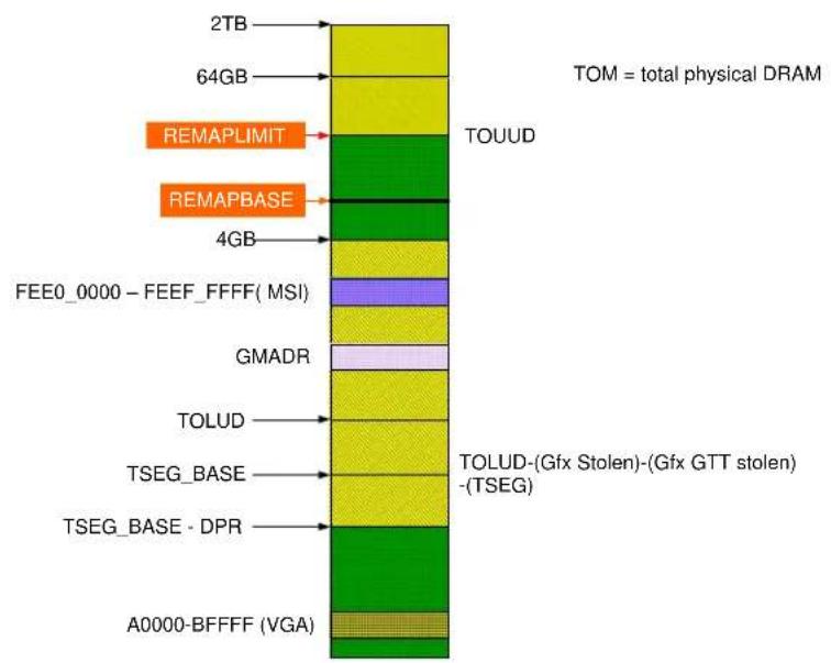
bar_stacked
| Memory Type | Value | | ------------------------ | ----- | | 2TB | | | 64GB | | | REMAPLIMIT | | | REMAPBASE | | | 4GB | | | FEE0_0000 - FEEF_FFFF(MSI) | | | GMADR | | | TOLUD | | | TSEG_BASE | | | TSEG_BASE - DPR | | | A0000-BFFFF (VGA) | |mem writes peer write (if matching PEG range else invalid)
mem reads invalid transaction
mem writes -Route based on SNR bit. mem reads -Route based on SNR bit.
mem writes -GPU (IntLogical/IntPhysical)
mem reads -Invalid transaction
mem writes -non-snoop mem write
mem reads -invalid transaction
mem writes peer write (based on Dev1 VGA en) else invalid mem reads invalid transaction
2.3.13.2 PCI Express\* Interface Decode Rules
All "SNOOP semantic" PCI Express transactions are kept coherent with processor caches.
All "Snoop not required semantic" cycles must reference the direct DRAM address range. PCI-Express non-snoop initiated cycles are not snooped.
If a "Snoop not required semantic" cycle is outside of the address range mapped to system memory, then it will proceed as follows:
- Reads: Sent to DRAM address 000C_0000h (non-snooped) and will return "unsuccessful completion".
- Writes: Sent to DRAM address 000C_0000h (non-snooped) with byte enables all disabled Peer writes from PEG to DMI are not supported.
If PEG bus master enable is not set, all reads and writes are treated as unsupported requests.
2.3.13.2.1 TC/ VC Mapping Details
• VC0 (enabled by default)
— Snoop port and Non-snoop Asynchronous transactions are supported.
— Internal Graphics GMADR writes can occur. Unlike FSB chipsets, these will NOT be snooped regardless of the snoop not required (SNR) bit.
— Internal Graphics GMADR reads (unsupported).
— Peer writes are only supported between PEG ports. PEG to DMI peer write accesses are NOT supported.
— MSI can occur. These will route to the cores (IntLogical/IntPhysical) regardless of the SNR bit.
- VC1 is not supported.
- VCm is not supported.
Figure 2-8. PEG Upstream VC0 Memory Map
Upstream Initiated VC0 Cycle Memory Map
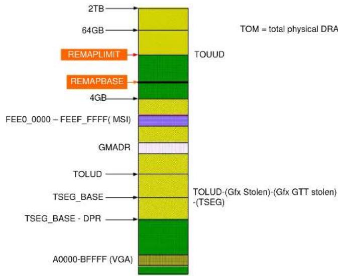
☐ mem writes peer write (if matching PEG range else invalid) mem reads invalid transaction
mem writes Route based on SNR bit. mem reads Route based on SNR bit.
mem writes -CPU (IntLogical/IntPhysical) mem reads -Invalid transaction
mem writes non-snoop mem write mem reads invalid transaction
mem writes invalid transaction mem reads invalid transaction
2.3.13.3 Legacy VGA and I/O Range Decode Rules
The legacy 128 KB VGA memory range 000A_0000h-000B_FFFFh can be mapped to IGD (Device 2), PCI Express (Device 1 functions or Device 6), and/or to the DMI Interface depending on the programming of the VGA steering bits. Priority for VGA mapping is constant in that the processor always decodes internally mapped devices first. Internal to the processor, decode precedence is always given to IGD. The processor always positively decodes internally mapped devices, namely the IGD. Subsequent decoding of regions mapped to either PCI Express port or the DMI Interface depends on the Legacy VGA configurations bits (VGA Enable and MDAP).
For the remainder of this section, PCI Express can refer to either the device 1 port functions or the device 6 port.
VGA range accesses will always be mapped as UC type memory.
Accesses to the VGA memory range are directed to IGD depend on the configuration. The configuration is specified by:
- Internal Graphics Controller in Device 2 is enabled (DEVEN.D2EN bit 4)
- Internal Graphics VGA in Device 0, function 0 is enabled through register GGC bit 1.
- IGD memory accesses (PCICMD2 04 - 05h, MAE bit 1) in Device 2 configuration space are enabled.
- VGA Compatibility Memory accesses (VGA Miscellaneous output Register - MSR Register, bit 1) are enabled.
- Software sets the proper value for VGA Memory Map Mode Register (VGA GR06 Register, bits 3-2). See Table 2-4 for translations.
Table 2-4. IGD Frame Buffer Accesses
| Mem Access→GR06(3:2) | A0000h-AFFFFh | B0000h-B7FFFhMDA | B8000h-BFFFFh |
| 00 IGD IGD | IGD | ||
| 01 IGD | PCI Express Bridge or DMI Interface | PCI Express Bridge or DMI Interface | |
| 10 | PCI Express Bridge or DMI Interface | IGD | PCI Express Bridge or DMI Interface |
| 11 | PCI Express Bridge or DMI Interface | PCI Express Bridge or DMI Interface | IGD |
Note: Additional qualification within IGD comprehends internal MDA support. The VGA and MDA enabling bits detailed below control segments not mapped to IGD.
VGA I/O range is defined as addresses where A[15:0] are in the ranges 03B0h to 03BBh, and 03C0h to 03DFh. VGA I/O accesses are directed to IGD depends on the following configuration.
- Internal Graphics Controller in Device 2 is enabled through register DEVEN.D2EN bit 4.
- Internal Graphics VGA in Device 0 function 0 is enabled through register GGC bit 1.
- IGD I/O accesses (PCICMD2 04 - 05h, IOAE bit 0) in Device 2 are enabled.
- VGA I/O decodes for IGD uses 16 address bits (15:0) there is no aliasing. Note that this is different when compared to a bridge device (Device 1) that used only 10 address bits (A 9:0) for VGA I/O decode.
- VGA I/O input/output address select (VGA Miscellaneous output Register - MSR Register, bit 0) used to select mapping of I/O access as defined in Table 2-5.
Table 2-5. IGD VGA I/ O Mapping
| I/O Access → MSRb0 | 3CX 3DX 3B0-3BB 3BC-3BF | |||
| 0 | IGD | PCI Express Bridge or DMI Interface | IGD | PCI Express Bridge or DMI Interface |
| 1 | IGD | IGD | PCI Express Bridge or DMI Interface | PCI Express Bridge or DMI Interface |
Note: Additional qualification within IGD comprehends internal MDA support. The VGA and MDA enabling bits detailed below control ranges not mapped to IGD.
For regions mapped outside of the IGD (or if IGD is disabled), the legacy VGA memory range A0000h-BFFFFh is mapped either to the DMI Interface or PCI Express depending on the programming of the VGA Enable bit in the BCTRL configuration register in the PEG configuration space, and the MDAPxx bits in the Legacy Access Control (LAC) register in Device 0 configuration space. The same register controls mapping VGA I/O address ranges. VGA I/O range is defined as addresses where A[9:0] are in the ranges 3B0h to 3BBh and 3C0h to 3DFh (inclusive of ISA address aliases – A[15:10] are not decoded). The function and interaction of these two bits is described below:
VGA Enable: Controls the routing of processor initiated transactions targeting VGA compatible I/O and memory address ranges. When this bit is set, the following processor accesses will be forwarded to the PCI-Express:
- memory accesses in the range 0A0000h to 0BFFFFh
- I/O addresses where A[9:0] are in the ranges 3B0h to 3BBh and 3C0h to 3DFh (including ISA address aliases - A[15:10] are not decoded)
When this bit is set to a 1:
Forwarding of these accesses issued by the processor is independent of the I/O address and memory address ranges defined by the previously defined base and limit registers.
Forwarding of these accesses is also independent of the settings of the ISA Enable settings if this bit is "1".
Accesses to I/O address range x3BCh-x3BFh are forwarded to DMI Interface.
When this bit is set to a 0:
Accesses to I/O address range x3BCh-x3BFh are treated just like any other I/O accesses. That is, the cycles are forwarded to PCI Express if the address is within IOBASE and IOLIMIT and ISA enable bit is not set; otherwise, they are forwarded to the DMI Interface.
VGA compatible memory and I/O range accesses are not forwarded to PCI Express but rather they are mapped to DMI Interface unless they are mapped to PCI Express using I/O and memory range registers defined above (IOBASE, IOLIMIT).
Table 2-6 shows the behavior for all combinations of MDA and VGA.
Table 2-6. VGA and MDA I/O Transaction Mapping
| VGA_en | MDAP Range | Destination | Ion Exceptions/ Notes |
| 0 0 VGA, MDA | DMI Interface | ||
| 0 1 Invalid Undefined behavior results | |||
| 1 0 VGA | PCI Express | ||
| 1 1 VGA | PCI Express | ||
| 1 | 1 | MDA | DMI Interface Note: x3BCh-x3BEh will also go to DMI Interface |
The same registers control mapping of VGA I/O address ranges. VGA I/O range is defined as addresses where A[9:0] are in the ranges 3B0h to 3BBh and 3C0h to 3DFh (inclusive of ISA address aliases – A[15:10] are not decoded). The function and interaction of these two bits is described below:
MDA Present (MDAP): This bit works with the VGA Enable bit in the BCTRL register of device 1 to control the routing of processor initiated transactions targeting MDA compatible I/O and memory address ranges. This bit should not be set when the VGA
Enable bit is not set. If the VGA enable bit is set, then accesses to I/O address range x3BCh-x3BFh are forwarded to DMI Interface. If the VGA enable bit is not set, then accesses to I/O address range x3BCh-x3BFh are treated just like any other I/O accesses. That is, the cycles are forwarded to PCI Express if the address is within IOBASE and IOLIMIT and ISA enable bit is not set; otherwise, they are forwarded to DMI Interface. MDA resources are defined as the following:
Memory: 0B0000h-0B7FFFh
I/O: 3B4h, 3B5h, 3B8h, 3B9h, 3BAh, 3BFh, (Including ISA address aliases, A[15:10] are not used in decode)
Any I/O reference that includes the I/O locations listed above, or their aliases, will be forwarded to the DMI Interface even if the reference includes I/O locations not listed above.
For I/O reads, which are split into multiple DWord accesses, this decode applies to each DWord independently. For example, a read to x3B3 and x3B4 (quadword read to x3B0 with BE# = E7h) will result in a DWord read from PEG at 3B0 (BE# = Eh), and a DWord read from DMI at 3B4 (BE=7h). Since the processor will not issue I/O writes crossing the DWord boundary, this special case does not exist for writes.
Summary of decode priority:
A) Internal Graphics VGA, if enabled, gets: 03C0h-03CFh: always 03B0h-03BBh: if MSR[0]=0 (MSR is I/O register 03C2h) 03D0h-03DFh: if MSR[0]=1 Note: 03BCh-03BFh never decodes to IGD; 3BCh-3BEh are parallel port I/Os, and 3BFh is only used by true MDA devices, apparently.
B) Else, If MDA Present (if VGA on PEG is enabled), DMI gets: x3B4,5,8,9,A,F (any access with any of these bytes enabled, regardless of the other BEs)
C) Else, If VGA on PEG is enabled, PEG gets: x3B0h-x3BBh x3C0h-x3CFh x3D0h-x3DFh
D) Else, if ISA Enable=1, DMI gets: upper 768 bytes of each 1K block
E) Else, IOBASE/IOLIMIT apply
2.4 Processor Register Introduction
The processor contains two sets of software accessible registers, accessed using the Host processor I/O address space – Control registers and internal configuration registers.
- Control registers are I/O mapped into the processor I/O space, which control access to PCI and PCI Express configuration space (see Section 2.4.1).
- Internal configuration registers residing within the processor are partitioned into three logical device register sets ("logical" since they reside within a single physical device). The first register set is dedicated to Host Bridge functionality (that is, DRAM configuration, other chipset operating parameters and optional features). The second register block is dedicated to Host-PCI Express Bridge functions (controls PCI Express interface configurations and operating parameters). The third register block is for the internal graphics functions.
The processor internal registers (I/O Mapped, Configuration and PCI Express Extended Configuration registers) are accessible by the Host processor. The registers that reside within the lower 256 bytes of each device can be accessed as Byte, Word (16 bit), or DWord (32 bit) quantities, with the exception of CONFIG_ADDRESS, which can only be accessed as a DWord. All multi-byte numeric fields use "little-endian" ordering (that is, lower addresses contain the least significant parts of the field). Registers that reside in bytes 256 through 4095 of each device may only be accessed using memory mapped transactions in DWord (32 bit) quantities.
Some of the processor registers described in this section contain reserved bits. These bits are labeled "Reserved". Software must deal correctly with fields that are reserved. On reads, software must use appropriate masks to extract the defined bits and not rely on reserved bits being any particular value. On writes, software must ensure that the values of reserved bit positions are preserved. That is, the values of reserved bit positions must first be read, merged with the new values for other bit positions and then written back. Note the software does not need to perform read, merge, and write operation for the Configuration Address Register.
In addition to reserved bits within a register, the processor contains address locations in the configuration space of the Host Bridge entity that are marked either "Reserved" or "Intel Reserved". The processor responds to accesses to Reserved address locations by completing the host cycle. When a Reserved register location is read, a zero value is returned. (Reserved registers can be 8-, 16-, or 32 bits in size). Writes to Reserved registers have no effect on the processor. Registers that are marked as Intel Reserved must not be modified by system software. Writes to Intel Reserved registers may cause system failure. Reads from Intel Reserved registers may return a non-zero value.
Upon a Full Reset, the processor sets its entire set of internal configuration registers to predetermined default states. Some register values at reset are determined by external strapping options. The default state represents the minimum functionality feature set required to successfully bringing up the system. Hence, it does not represent the optimal system configuration. It is the responsibility of the system initialization software (usually BIOS) to properly determine the DRAM configurations, operating parameters and optional system features that are applicable, and to program the processor registers accordingly.
2.4.1 I/O Mapped Registers
The processor contains two registers that reside in the processor I/O address space—the Configuration Address (CONFIG_ADDRESS) Register and the Configuration Data (CONFIG_DATA) Register. The Configuration Address Register enables/disables the configuration space and determines what portion of configuration space is visible through the Configuration Data window.
2.5 PCI Device 0, Function 0 Configuration Registers
Table 2-7 lists the registers arranged by address offset. Register bit descriptions are in the sections following the table.
Table 2-7. PCI Device 0, Function 0 Register Address Map (Sheet 1 of 2)
| Address Offset | Register Symbol | Register Name Reset Value Access | ||
| 0-1h VID | Vendor Identification 8086h RO | |||
| 2-3h DID | Device Identification 0100h RO-FW, RO-V | |||
| 4-5h PCI | CMD PCI Command 0006h RO RW | |||
| 6-7h | PCI/STS PCI Status 0090h RO, RW1C | |||
| 8h | RID | Revision Identification | 00h | RO-FW |
| 9-Bh | CC | Class Code | 06_0000h | RO |
| C-Dh | RSVD | Reserved | 0h | RO |
| Eh HDR | Header Type 00h RO | |||
| F-2Bh | RSVD | Reserved | 0h | RO |
| 2C-2Dh | SVID | Subsystem Vendor Identification | 0000h | RW-O |
| 2E-2Fh | SID | Subsystem Identification | 0000h | RW-O |
| 30-33h | RSVD | Reserved | 0h | RO |
| 34h | RSVD | Reserved | E0h | RO |
| 35-3Fh RSVD Reserved 0h RO | ||||
| 40-47h PX | PEPBAR | PCI Express Egress Port Base Address | 0000_0000_0000_0000h | RW |
| 48-4Fh | MCHBAR | Host Memory Mapped Register Range Base | 0000_0000_0000_0000h | RW |
| 50-51h | GGC | GMCH Graphics Control Register | 0028h | RW-KL, RW-L |
| 52-53h | RSVD | Reserved | 0h | RO |
| 54-57h | DEVEN | Device Enable | 0000_209Fh | RW-L, RO, RW |
| 58-5Bh | PAVPC | Protected Audio Video Path Control | 0000_0000h | RW-L, RW-KL |
| 5C-5Fh | DPR | DMA Protected Range | 0000_0000h | RW-L, RO-V,RW-KL |
| 60-67h | PCIEXBAR | PCI Express Register Range Base Address | 0000_0000_0000_0000h | RW, RW-V |
| 68-6Fh | DMIBAR | Root Complex Register Range Base Address | 0000_0000_0000_0000h | RW |
| 70-77h | RSVD | Reserved | 0000_007F_FFF0_0000h | RW-L |
| 78-7Fh RSVD | Reserved | 0000_0000_0000_0000h | RW-L, RW-KL | |
| 80h | PAMO | Programmable Attribute Map 0 | 00h | RW |
Table 2-7. PCI Device 0, Function 0 Register Address Map (Sheet 2 of 2)
| Address Offset | Register Symbol | Register Name | Reset Value | Access |
| 81h PAM1 | Programmable | Attribute Map 1 00h RW | ||
| 82h PAM2 | Programmable | Attribute Map 2 00h RW | ||
| 83h PAM3 | Programmable | Attribute Map 3 00h RW | ||
| 84h PAM4 | Programmable | Attribute Map 4 00h RW | ||
| 85h PAM5 | Programmable | Attribute Map 5 00h RW | ||
| 86h PAM6 | Programmable | Attribute Map 6 00h RW | ||
| 87h LAC | Legacy Access Control 00h RW | |||
| 88h RSVD | Reserved | 02h | RW-L, RW-KL,RW-LV, RO | |
| 89-8Fh RSVD Reserved 0h RO | ||||
| 90-97h REMAPBASE | Remap Base Address Register | 0000_000F_FFF0_0000h | RW-KL, RW-L | |
| 98-9Fh | REMAPLIMIT | Remap Limit Address Register | 0000_0000_0000_0000h | RW-KL, RW-L |
| A0-A7h | TOM | Top of Memory | 0000_007F_FFF0_0000h | RW-KL, RW-L |
| A8-AFh | TOUUD | Top of Upper Usable DRAM | 0000_0000_0000_0000h | RW-KL, RW-L |
| B0-B3h | BDSM | Base Data of Stolen Memory | 0000_0000h | RW-KL, RW-L |
| B4-B7h | BGSM | Base of GTT stolen Memory | 0010_0000h | RW-KL, RW-L |
| B8-BBh | TSEGMB | TSEG Memory Base | 0000_0000h | RW-KL, RW-L |
| BC-BFh | TOLUD | Top of Low Usable DRAM | 0010_0000h | RW-KL, RW-L |
| C0- | RSVD | Reserved 0h RO | ||
| C8-C9h | ERRSTS | Error Status | 0000h | RW1CS |
| CA-CBh | ERRCMD | Error Command | 0000h | RW |
| CC-CDh | SMICMD | SMI Command | 0000h | RW |
| CE-CFh SCICMD SCI Command | 0000h | RW | ||
| D0-DBh | RSVD | Reserved 0h RO | ||
| DC-DFh | SKPD | Scratchpad Data | 0000_0000h | RW |
| E0-E3h RSVD Reserved 0h RO | ||||
| E4-E7h | CAPID0_A | Capabilities A | 0000_0000h | RO-FW, RO-KFW |
| E8-EBh | RSVD | Reserved | 0000_0000h | RO-FW |
2.5.1 VID—Vendor Identification Register
This register, combined with the Device Identification register, uniquely identifies any PCI device.
| B/ D/ F/ Type: 0/ 0/ 0/ PCIAddress Offset: 0-1hReset Value: 8086hAccess: ROSize: 16 bits | ||||
| Bit Attr | ResetValue | RST/PWR | Description | |
| 15:0 RO 8086h Uncore | Vendor Identification Number (VID)PCI standard identification for Intel. | |||
2.5.2 DID—Device Identification Register
This register, combined with the Vendor Identification register, uniquely identifies any PCI device.
| B/ D/ F/ Type: 0/ 0/ 0/ PCIAddress Offset: 2-3hReset Value: 0100hAccess: RO-FW, RO-VSize: 16 bits | ||||
| Bit Attr | ResetValue | RST/PWR | Description | |
| 15:4 RO-FW | 010h | Uncore | Device Identification Number MSB (DID_MSB)This is the upper part of device identification assigned to the processor. | |
| 3:2 | RO-V | 00b | Uncore | Device Identification Number SKU (DID_SKU)This is the middle part of device identification assigned to the processor. |
| 1:0 | RO-FW | 00b | Uncore | Device Identification Number LSB (DID_LSB)This is the lower part of device identification assigned to the processor. |
2.5.3 PCI CMD—PCI Command Register
Since Device 0 does not physically reside on PCI_A, many of the bits are not implemented.
| B/ D/ F/ Type: 0/ 0/ 0/ PCIAddress Offset: 4-5hReset Value: 0006hAccess: RO, RWSize: 16 bitsBIOS Optimal Default 00h | ||||
| Bit Attr | Reset Value | RST/PWR | Description | |
| 15:10 RO 0h Reserved | ||||
| 9 RO 0b Uncore | Fast Back-to-Back Enable (FB2B)This bit controls whether or not the master can do fast back-to-back write. Since device 0 is strictly a target this bit is not implemented and is hardwired to 0. Writes to this bit position have no effect. | |||
| 8 RW 0b Uncore | SERR Enable (SERRE)This bit is a global enable bit for Device 0 SERR messaging. The processor communicates the SERR condition by sending an SERR message over DMI to the PCH.1 = The processor is enabled to generate SERR messages over DMI for specific Device 0 error conditions that are individually enabled in the ERRCMD and DMIUEMSK registers. The error status is reported in the ERRSTS, PCISTS, and DMIUEST registers.0 = The SERR message is not generated by the Host for Device 0. This bit only controls SERR messaging for Device 0. Other integrated devices have their own SERRE bits to control error reporting for error conditions occurring in each device. The control bits are used in a logical OR manner to enable the SERR DMI message mechanism.0 = Device 0 SERR disabled1 = Device 0 SERR enabled | |||
| 7 RO 0b Uncore | Address/ Data Stepping Enable (ADSTEP)Address/data stepping is not implemented in the processor, and this bit is hardwired to 0. Writes to this bit position have no effect. | |||
| 6 RW 0b Uncore | Parity Error Enable (PERRE)This bit controls whether or not the Master Data Parity Error bit in the PCI Status register can bet set.0 = Disable. Master Data Parity Error bit in PCI Status register can NOT be set.1 = Enable. Master Data Parity Error bit in PCI Status register CAN be set. | |||
| 5 RO 0b Uncore | VGA Palette Snoop Enable (VGASNOOP)The processor does not implement this bit and it is hardwired to a 0. Writes to this bit position have no effect. | |||
| 4 RO 0b Uncore | Memory Write and Invalidate Enable (MWIE)The processor will never issue memory write and invalidate commands. This bit is therefore hardwired to 0. Writes to this bit position will have no effect. | |||
| 3 RO 0h Reserved | ||||
| Bit Attr | Reset Value | RST/PWR | Description | |
| 2 RO 1b Uncore | Bus Master Enable (BME)The processor is always enabled as a master on the backbone. This bit is hardwired to a 1. Writes to this bit position have no effect. | |||
| 1 RO 1b Uncore | Memory Access Enable (MAE)The processor always allows access to main memory, except when such access would violate security principles. Such exceptions are outside the scope of PCI control. This bit is not implemented and is hardwired to 1. Writes to this bit position have no effect. | |||
| 0 RO 0b Uncore | I/ O Access Enable (IOAE)This bit is not implemented in the processor and is hardwired to a 0. Writes to this bit position have no effect. | |||
2.5.4 PCI STS—PCI Status Register
This status register reports the occurrence of error events on Device 0's PCI interface. Since Device 0 does not physically reside on PCI_A, many of the bits are not implemented.
| B/ D/ F/ Type: 0/ 0/ 0/ PCIAddress Offset: 6-7hReset Value: 0090hAccess: RO, RW1CSize: 16 bitsBIOS Optimal Default 00h | ||||
| Bit Attr | Reset Value | RST/PWR | Description | |
| 15 RW1C | 0b | Uncore | Detected Parity Error (DPE)This bit is set when this Device receives a Poisoned TLP. | |
| 14 RW1C | 0b | Uncore | Signaled System Error (SSE)This bit is set to 1 when Device 0 generates an SERR message over DMI for any enabled Device 0 error condition. Device 0 error conditions are enabled in the PCICMD, ERRCMD, and DMIUEMSK registers. Device 0 error flags are read/reset from the PCISTS, ERRSTS, or DMIUEST registers. Software clears this bit by writing a 1 to it. | |
| 13 RW1C | 0b | Uncore | Received Master Abort Status (RMAS)This bit is set when the processor generates a DMI request that receives an Unsupported Request completion packet. Software clears this bit by writing a 1 to it. | |
| 12 RW1C | 0b | Uncore | Received Target Abort Status (RTAS)This bit is set when the processor generates a DMI request that receives a Completer Abort completion packet. Software clears this bit by writing a 1 to it. | |
| 11 | RO 0b | Uncore | Signaled Target Abort Status (STAS)The processor will not generate a Target Abort DMI completion packet or Special Cycle. This bit is not implemented and is hardwired to a 0. Writes to this bit position have no effect. | |
| Bit | Attr | Reset Value | RST/PWR | Description |
| 10:9 RO 00b Uncore | DEVSEL Timing (DEVT)These bits are hardwired to "00". Writes to these bit positions have no effect. Device 0 does not physically connect to PCI_A. These bits are set to "00" (fast decode) so that optimum DEVSEL timing for PCI_A is not limited by the Host. | |||
| 8 RW1C 0b Uncore | Master Data Parity Error Detected (DPD)This bit is set when DMI received a Poisoned completion from PCH.This bit can only be set when the Parity Error Enable bit in the PCI Command register is set. | |||
| 7 RO 1b Uncore | Fast Back-to-Back (FB2B)This bit is hardwired to 1. Writes to these bit positions have no effect. Device 0 does not physically connect to PCI_A. This bit is set to 1 (indicating fast back-to-back capability) so that the optimum setting for PCI_A is not limited by the Host. | |||
| 6 RO 0h Reserved | ||||
| 5 RO 0b Uncore | 66 MHz Capable (MC66)Does not apply to PCI Express. Must be hardwired to 0. | |||
| 4 RO 1b Uncore | Capability List (CLI ST)This bit is hardwired to 1 to indicate to the configuration software that this device/function implements a list of new capabilities. A list of new capabilities is accessed using register CAPPTR at configuration address offset 34h. Register CAPPTR contains an offset pointing to the start address within configuration space of this device where the Capability Identification register resides. | |||
| 3:0 RO 0h Reserved | ||||
2.5.5 RID—Revision Identification Register
This register contains the revision number of Device 0. These bits are read only and writes to this register have no effect.
This register contains the revision number of the processor. The Revision ID (RID) is a traditional 8-bit Read Only (RO) register located at offset 08h in the standard PCI header of every PCI/PCI Express compatible device and function. Following reset, the SRID is returned when the RID is read at offset 08h. The SRID value reflects the actual product stepping. To select the CRID value, BIOS/configuration software writes a key value of 69h to Bus 0, Device 0, Function 0 (DMI device) of the processor RID register at offset 08h. This causes the CRID to be returned when the RID is read at offset 08h.
Stepping Revision ID (SRID)
This register contains the revision number of the processor. The SRID is a 8-bit hardwired value assigned by Intel, based on product stepping. The SRID is not a directly addressable PCI register. The SRID value is reflected through the RID register when appropriately addressed.
Compatible Revision ID (CRID)
The CRID is an 8-bit hardwired value assigned by Intel during manufacturing process. Normally, the value assigned as the CRID will be identical to the SRID value of a previous stepping of the product with which the new product is deemed "compatible". The CRID is not a directly addressable PCI register. The CRID value is reflected through the RID register when appropriately addressed.
| B/ D/ F/ Type: 0/ 0/ 0/ PCIAddress Offset: 8hReset Value: 00hAccess: RO-FWSize: 8 bits | ||||
| Bit Attr | ResetValue | RST/PWR | Description | |
| 7:0 RO-FW 00h | Uncore | Revision Identification Number (RID)This is an 8-bit value that indicates the revision identification number for the Processor Device 0. Refer to the Intel® Xeon® Processor E3-1200 Family Specification Update for the value of the RID register. | ||
2.5.6 CC—Class Code Register
This register identifies the basic function of the device, a more specific sub-class, and a register-specific programming interface.
| B/ D/ F/ Type: 0/ 0/ 0/ PCIAddress Offset: 9-BhReset Value: 06_0000hAccess: ROSize: 24 bits | ||||
| Bit Attr | ResetValue | RST/PWR | Description | |
| 23:16 RO 06h Uncore | Base Class Code (BCC)This is an 8-bit value that indicates the base class code for the Host Bridge device. This code has the value 06h, indicating a Bridge device. | |||
| 15:8 RO 00h Uncore | Sub-Class Code (SUBCC)This is an 8-bit value that indicates the category of Bridge into which the Host Bridge device falls. The code is 00h indicating a Host Bridge. | |||
| 7:0 RO 00h Uncore | Programming Interface (PI)This is an 8-bit value that indicates the programming interface of this device. This value does not specify a particular register set layout and provides no practical use for this device. | |||
2.5.7 HDR—Header Type Register
This register identifies the header layout of the configuration space. No physical register exists at this location.
| B/ D/ F/ Type: 0/ 0/ 0/ PCIAddress Offset: EhReset Value: 00hAccess: ROSize: 8 bits | ||||
| Bit Attr | ResetValue | RST/PWR | Description | |
| 7:0 RO 00h Uncore | PCI Header (HDR)This field always returns 0 to indicate that the Host Bridge is a single function device with standard header layout. Reads and writes to this location have no effect. | |||
2.5.8 SVID—Subsystem Vendor Identification Register
This value is used to identify the vendor of the subsystem.
| B/ D/ F/ Type: 0/ 0/ 0/ PCIAddress Offset: 2C-2DhReset Value: 0000hAccess: RW-OSize: 16 bits | ||||
| Bit Attr | ResetValue | RST/PWR | Description | |
| 15:0 RW-O 0000h | Uncore | Subsystem Vendor ID (SUBVID)This field should be programmed during boot-up to indicate the vendor of the system board. After it has been written once, it becomes read only. | ||
2.5.9 SID—Subsystem Identification Register
This value is used to identify a particular subsystem.
| B/ D/ F/ Type: 0/ 0/ 0/ PCIAddress Offset: 2E-2FhReset Value: 0000hAccess: RW-OSize: 16 bits | ||||
| Bit Attr | ResetValue | RST/PWR | Description | |
| 15:0 RW-O 0000h | Uncore | Subsystem ID (SUBID)This field should be programmed during BIOS initialization. After it has been written once, it becomes read only. | ||
2.5.10 PXPEPBAR—PCI Express Egress Port Base Address Register
This is the base address for the PCI Express Egress Port MMIO Configuration space. There is no physical memory within this 4 KB window that can be addressed. The 4 KB reserved by this register does not alias to any PCI 2.3 compliant memory mapped space. On reset, the EGRESS port MMIO configuration space is disabled and must be enabled by writing a 1 to PXPEPBAREN [Device 0, offset 40h, bit 0].
All the bits in this register are locked in Intel TXT mode.
| B/ D/ F/ Type: 0/ 0/ 0/ PCIAddress Offset: 40-47hReset Value: 0000_0000_0000_0000hAccess: RWSize: 64 bitsBIOS Optimal Default 0_0000_0000h | ||||
| Bit Attr | ResetValue | RST/PWR | Description | |
| 63:39 RO 0h Reserved | ||||
| 38:12 RW 0000000h Uncore | PCI Express Egress Port MMIO Base Address (PXPEPBAR)This field corresponds to bits 38:12 of the base address PCIExpress Egress Port MMIO configuration space. BIOS will program this register resulting in a base address for a 4 KB block of contiguous memory address space. This register ensures that a naturally aligned 4 KB space is allocated within the first 512 GB of addressable memory space. System Software uses this base address to program the PCI Express Egress Port MMIO register set. All the bits in this register are locked in Intel TXT mode. | |||
| 11:1 RO 0h Reserved | ||||
| 0 | RW | 0b | Uncore | PXPEPBAR Enable (PXPEPBAREN)0 = Disabled. PXPEPBAR is disabled and does not claim any memory1 = Enabled. PXPEPBAR memory mapped accesses are claimed and decoded appropriatelyThis register is locked by Intel TXT. |
2.5.11 MCHBAR—Host Memory Mapped Register Range Base Register
This is the base address for the Host Memory Mapped Configuration space. There is no physical memory within this 32 KB window that can be addressed. The 32 KB reserved by this register does not alias to any PCI 2.3 compliant memory mapped space. On reset, the Host MMIO Memory Mapped Configuration space is disabled and must be enabled by writing a 1 to MCHBAREN [Device 0, offset 48h, bit 0].
All the bits in this register are locked in Intel TXT mode.
The register space contains memory control, initialization, timing, and buffer strength registers; clocking registers; and power and thermal management registers.
| B/ D/ F/ Type: 0/ 0/ 0/ PCIAddress Offset: 48-4FhReset Value: 0000_0000_0000_0000hAccess: RWSize: 64 bitsBI OS Optimal Default 00_0000_0000h | |||||||
| Bit Attr | ResetValue | RST/PWR | Description | ||||
| 63:39 RO 0h Reserved | |||||||
| 38:15 RW 000000h Uncore | Host Memory Mapped Base Address (MCHBAR)This field corresponds to bits 38:15 of the base address HostMemory Mapped configuration space. BIOS will program thisregister resulting in a base address for a 32 KB block of contiguousmemory address space. This register ensures that a naturallyaligned 32 KB space is allocated within the first 512 GB ofaddressable memory space. System Software uses this baseaddress to program the Host Memory Mapped register set. All thebits in this register are locked in Intel TXT mode. | ||||||
| 14:1 RO 0h | Reserved | ||||||
| 0 | RW | 0b | Uncore | MCHBAR Enable (MCHBAREN)0 = Disabled. MCHBAR is disabled and does not claim any memory1 = Enabled. MCHBAR memory mapped accesses are claimed and decoded appropriatelyThis register is locked by Intel TXT. | |||
2.5.12 GGC—GMCH Graphics Control Register Register
All the bits in this register are Intel TXT lockable.
| B/ D/ F/ Type: 0/ 0/ 0/ PCIAddress Offset: 50-51hReset Value: 0028hAccess: RW-KL, RW-LSize: 16 bitsBIOS Optimal Default 00h | ||||
| Bit Attr | Reset Value | RST/PWR | Description | |
| 15 RO 0h Reserved | ||||
| 14 RW-L 0b Uncore Reserved | ||||
| 13:10 RO 0h Reserved | ||||
| 9:8 | RW-L 0h Uncore | GTT Graphics Memory Size (GGMS)This field is used to select the amount of Main Memory that is pre-allocated to support the Internal Graphics Translation Table. The BIOS ensures that memory is pre-allocated only when Internal graphics is enabled.GSM is assumed to be a contiguous physical DRAM space with DSM, and BIOS needs to allocate a contiguous memory chunk.Hardware will derive the base of GSM from DSM only using the GSM size programmed in the register.Hardware functionality in case of programming this value to Reserved is not ensured.Encoding:1h = 1 MB of pre-allocated memory2h = 2 MB of pre-allocated memory3h = Reserved0h = No pre-allocated memory | ||
| 7:3 | RW-L 05h Uncore | Graphics Mode Select (GMS)This field is used to select the amount of main memory that is pre-allocated to support the Internal Graphics device in VGA (non-linear) and Native (linear) modes. BIOS ensures that memory is pre-allocated only when internal graphics is enabled.This register is also Intel TXT lockable.Hardware does not clear or set any of these bits automatically based on IGD being disabled/enabled.BIOS Requirement: BIOS must not set this field to 0h if IVD (bit 1 of this register) is 0.0h = 0 MB1h = 32 MB2h = 64 MB3h = 96 MB4h = 128 MB5h = 160 MB6h = 192 MB7h = 224 MB8h = 256 MB9h = 288 MBAh = 320 MBBh = 352 MBCh = 384 MBDh = 416 MBEh = 448MBFh = 480 MB10h = 512 MBOther = Reserved | ||
| B/ D/ F/ Type: 0/ 0/ 0/ PCIAddress Offset: 50–51hReset Value: 0028hAccess: RW-KL, RW-LSize: 16 bitsBIOS Optimal Default 00h | ||||
| Bit | Attr | ResetValue | RST/PWR | Description |
| 2 RO | 0h Reserved | |||
| 1 RW-L | 0b Uncore | IGD VGA Disable (IVD)0 = Enable. Device 2 (IGD) claims VGA memory and I/O cycles,the Sub-Class Code within Device 2 Class Code register is 00.1 = Disable. Device 2 (IGD) does not claim VGA cycles (Memoryand I/O), and the Sub- Class Code field within Device 2function 0 Class Code register is 80h.BIOS Requirement: BIOS must not set this bit to 0 if the GMSfield (bits 7:3 of this register) pre-allocates no memory.This bit MUST be set to 1 if Device 2 is disabled using a register (DEVEN[3] = 0).This register is locked by Intel TXT lock. | ||
| 0 RW- | KL 0b Uncore | GGC Lock (GGCLCK)When set to 1b, this bit will lock all bits in this register. | ||
2.5.13 DEVEN—Device Enable Register
This register allows for enabling/disabling of PCI devices and functions that are within the processor package. In the following table the bit definitions describe the behavior of all combinations of transactions to devices controlled by this register.
All the bits in this register are Intel TXT Lockable.
| B/ D/ F/ Type: 0/ 0/ 0/ PCIAddress Offset: 54-57hReset Value: 0000_209FhAccess: RW-L, RO, RWSize: 32 bitsBIOS Optimal Default 00_0000h | ||||
| Bit Attr | Reset Value | RST/PWR | Description | |
| 31:15 RO 0h Reserved | ||||
| 14 RO 0h Reserved | ||||
| 13 RW-L 1b Uncore | PEG60 Enable (D6F0EN)0 = Disabled. Bus 0 Device 6 Function 0 is disabled and hidden.1 = Enabled. Bus 0 Device 6 Function 0 is enabled and visible.This bit will be set to 0b and remain 0b if PEG60 capability is disabled. | |||
| 12:8 RO 0h Reserved | ||||
| 7 | RO 0h Reserved | |||
| 6:5 | RO 0h Reserved | |||
| 4 | RW-L 1b | Uncore | Internal Graphics Engine (D2EN)0 = Disabled. Bus 0 Device 2 is disabled and hidden1 = Enabled. Bus 0 Device 2 is enabled and visibleThis bit will be set to 0b and remain 0b if Device 2 capability is disabled. | |
| 3 | RW-L 1b | Uncore | PEG10 Enable (D1F0EN)0 = Disabled. Bus 0 Device 1 Function 0 is disabled and hidden.1 = Enabled. Bus 0 Device 1 Function 0 is enabled and visible.This bit will be set to 0b and remain 0b if PEG10 capability is disabled. | |
| 2 | RW-L 1b | Uncore | PEG11 Enable (D1F1EN)0 = Disabled. Bus 0 Device 1 Function 1 is disabled and hidden.1 = Enabled. Bus 0 Device 1 Function 1 is enabled and visible.This bit will be set to 0b and remain 0b if:PEG11 is disabled by strap (PEG0CFGSEL) | |
| 1 | RW-L 1b | Uncore | PEG12 Enable (D1F2EN)0 = Disabled. Bus 0 Device 1 Function 2 is disabled and hidden.1 = Enabled. Bus 0 Device 1 Function 2 is enabled and visible.This bit will be set to 0b and remain 0b if:PEG12 is disabled by strap (PEG0CFGSEL) | |
| 0 | RO 1b | Uncore | Host Bridge (D0EN)Bus 0 Device 0 Function 0 may not be disabled and is therefore hardwired to 1. | |
2.5.14 PCI EXBAR—PCI Express Register Range Base Address Register
This is the base address for the PCI Express configuration space. This window of addresses contains the 4 KB of configuration space for each PCI Express device that can potentially be part of the PCI Express Hierarchy associated with the Uncore. There is no actual physical memory within this window of up to 256 MB that can be addressed. The actual size of this range is determined by a field in this register.
Each PCI Express Hierarchy requires a PCI Express Base register. The Uncore supports one PCI Express Hierarchy. The region reserved by this register does not alias to any PCI2.3 compliant memory mapped space. For example, the range reserved for MCHBAR is outside of PCIEXBAR space.
On reset, this register is disabled and must be enabled by writing a 1 to the enable field in this register. This base address shall be assigned on a boundary consistent with the number of buses (defined by the length field in this register), above TOLUD and still within 39-bit addressable memory space.
The PCI Express Base Address cannot be less than the maximum address written to the Top of physical memory register (TOLUD). Software must ensure that these ranges do not overlap with known ranges located above TOLUD.
Software must ensure that the sum of the length of the enhanced configuration region + TOLUD + any other known ranges reserved above TOLUD is not greater than the 39-bit addressable limit of 512 GB. In general, system implementation and the number of PCI/PCI Express/PCI-X buses supported in the hierarchy will dictate the length of the region.
All the bits in this register are locked in Intel TXT mode.
| B/ D/ F/ Type: 0/ 0/ 0/ PCIAddress Offset: 60-67hReset Value: 0000_0000_0000_0000hAccess: RW, RW-VSize: 64 bitsBIOS Optimal Default 0000_0000_0000h | ||||
| Bit Attr | ResetValue | RST/PWR | Description | |
| 63:39 RO 0h Reserved | ||||
| 38:28 RW 000h Uncore | PCI Express Base Address (PCI EXBAR)This field corresponds to bits 38:28 of the base address for PCIExpress enhanced configuration space. BIOS will program thisregister resulting in a base address for a contiguous memoryaddress space. The size of the range is defined by bits 2:1 of thisregister.This base address shall be assigned on a boundary consistent withthe number of buses (defined by the Length field in this register)above TOLUD and still within the 39-bit addressable memoryspace. The address bits decoded depend on the length of theregion defined by this register.This register is locked by Intel TXT.The address used to access the PCI Express configuration space fora specific device can be determined as follows:PCI Express Base Address + Bus Number * 1MB + DeviceNumber * 32KB + Function Number * 4KBThis address is the beginning of the 4 KB space that contains boththe PCI compatible configuration space and the PCI Expressextended configuration space. | |||
| 27 RW-V | 0b Uncore | 128MB Base Address Mask (ADMSK128)This bit is either part of the PCI Express Base Address (RW) or partof the Address Mask (RO, read 0b), depending on the value of bits[2:1] in this register. | ||
| 26 RW-V | 0b Uncore | 64MB Base Address Mask (ADMSK64)This bit is either part of the PCI Express Base Address (RW) or partof the Address Mask (RO, read 0b), depending on the value of bits[2:1] in this register. | ||
| 25:3 | RO 0h Reserved | |||
| 2:1 | RW | 00b | Uncore | Length (LENGTH)This field describes the length of this region.00 = 256 MB (buses 0-255). Bits 38:28 are decoded in the PCIExpress Base Address field.01 = 128 MB (buses 0-127). Bits 38:27 are decoded in the PCIExpress Base Address field.10 = 64 MB (buses 0-63). Bits 38:26 are decoded in the PCIExpress Base Address field.11 = Reserved.This register is locked by Intel TXT. |
| 0 | RW | 0b | Uncore | PCI EXBAR Enable (PCI EXBAREN)0 = The PCIEXBAR register is disabled. Memory read and writetransactions proceed as if there were no PCIEXBAR register.PCIEXBAR bits 38:26 are RW with no functionality behindthem.1 = The PCIEXBAR register is enabled. Memory read and writetransactions whose address bits 38:26 match PCIEXBAR willbe translated to configuration reads and writes within theUncore. These translated cycles are routed as shown in theabove table.This register is locked by Intel TXT. |
2.5.15 DMI BAR—Root Complex Register Range Base Address Register
This is the base address for the Root Complex configuration space. This window of addresses contains the Root Complex Register set for the PCI Express Hierarchy associated with the Host Bridge. There is no physical memory within this 4 KB window that can be addressed. The 4 KB reserved by this register does not alias to any PCI 2.3 compliant memory mapped space. On reset, the Root Complex configuration space is disabled and must be enabled by writing a 1 to DMIBAREN [Device 0, offset 68h, bit 0].
All the bits in this register are locked in Intel TXT mode.
| B/ D/ F/ Type: 0/ 0/ 0/ PCIAddress Offset: 68-6FhReset Value: 0000_0000_0000_0000hAccess: RWSize: 64 bitsBIOS Optimal Default 0_0000_0000h | ||||
| Bit Attr | Reset Value | RST/PWR | Description | |
| 63:39 RO 0h Reserved | ||||
| 38:12 RW 0000000h Uncore | DMI Base Address (DMI BAR)This field corresponds to bits 38:12 of the base address DMI configuration space. BIOS will program this register resulting in a base address for a 4 KB block of contiguous memory address space. This register ensures that a naturally aligned 4 KB space is allocated within the first 512 GB of addressable memory space. System Software uses this base address to program the DMI register set. All the Bits in this register are locked in Intel TXT mode. | |||
| 11:1 RO 0h | Reserved | |||
| 0 | RW | 0b | Uncore | DMI BAR Enable (DMI BAREN)0 = Disabled. DMIBAR is disabled and does not claim any memory1 = Enabled. DMIBAR memory mapped accesses are claimed and decoded appropriatelyThis register is locked by Intel TXT. |
2.5.16 PAM0—Programmable Attribute Map 0 Register
This register controls the read, write and shadowing attributes of the BIOS range from F_0000h to F_FFFFh. The Uncore allows programmable memory attributes on 13 legacy memory segments of various sizes in the 768 KB to 1 MB address range. Seven Programmable Attribute Map (PAM) registers are used to support these features. Cacheability of these areas is controlled using the MTRR register in the core.
Two bits are used to specify memory attributes for each memory segment. These bits apply to host accesses to the PAM areas. These attributes are:
- RE – Read Enable. When RE=1, the host read accesses to the corresponding memory segment are claimed by the Uncore and directed to main memory. Conversely, when RE=0, the host read accesses are directed to DMI.
- WE – Write Enable. When WE=1, the host write accesses to the corresponding memory segment are claimed by the Uncore and directed to main memory. Conversely, when WE=0, the host read accesses are directed to DMI.
The RE and WE attributes permit a memory segment to be Read Only, Write Only, Read/Write or Disabled. For example, if a memory segment has RE=1 and WE=0, the segment is Read Only.
| B/ D/ F/ Type: 0/ 0/ 0/ PCIAddress Offset: 80hReset Value: 00hAccess: RWSize: 8 bitsBIOS Optimal Default 00h | ||||
| Bit Attr | ResetValue | RST/PWR | Description | |
| 7:6 RO | 0h Reserved | |||
| 5:4 | RW | 00b Uncore | 0F0000-0FFFF Attribute (HI ENABLE)This field controls the steering of read and write cycles thataddress the BIOS area from 0F_0000h to 0F_FFFFh.00 = DRAM Disabled. All accesses are directed to DMI.01 = Read Only. All reads are sent to DRAM, all writes areforwarded to DMI.10 = Write Only. All writes are sent to DRAM, all reads are servicedby DMI.11 = Normal DRAM Operation. All reads and writes are serviced byDRAM.This register is locked by Intel TXT. | |
| 3:0 RO | 0h Reserved | |||
2.5.17 PAM1—Programmable Attribute Map 1 Register
This register controls the read, write and shadowing attributes of the BIOS range from C_0000h to C_7FFFh. The Uncore allows programmable memory attributes on 13 legacy memory segments of various sizes in the 768 KB to 1 MB address range. Seven Programmable Attribute Map (PAM) registers are used to support these features. Cacheability of these areas is controlled using the MTRR register in the core.
Two bits are used to specify memory attributes for each memory segment. These bits apply to host accesses to the PAM areas. These attributes are:
- RE – Read Enable. When RE=1, the host read accesses to the corresponding memory segment are claimed by the Uncore and directed to main memory. Conversely, when RE=0, the host read accesses are directed to DMI.
- WE – Write Enable. When WE=1, the host write accesses to the corresponding memory segment are claimed by the Uncore and directed to main memory. Conversely, when WE=0, the host read accesses are directed to DMI.
The RE and WE attributes permit a memory segment to be Read Only, Write Only, Read/Write or Disabled. For example, if a memory segment has RE=1 and WE=0, the segment is Read Only.
| B/ D/ F/ Type: 0/ 0/ 0/ PCIAddress Offset: 81hReset Value: 00hAccess: RWSize: 8 bitsBI OS Optimal Default 0h | ||||
| Bit Attr | Reset Value | RST/PWR | Description | |
| 7:6 RO 0h Reserved | ||||
| 5:4 RW 00b Uncore | 0C4000-0C7FFF Attribute (HI ENABLE)This field controls the steering of read and write cycles that address the BIOS area from 0C_4000h to 0C_7FFFh.00 = DRAM Disabled. All accesses are directed to DMI.01 = Read Only. All reads are sent to DRAM, all writes are forwarded to DMI.10 = Write Only. All writes are sent to DRAM, all reads are serviced by DMI.11 = Normal DRAM Operation. All reads and writes are serviced by DRAM.This register is locked by Intel TXT. | |||
| 3:2 RO 0h Reserved | ||||
| 1:0 RW 00b Uncore | 0C0000-0C3FFF Attribute (LOENABLE)This field controls the steering of read and write cycles that address the BIOS area from 0C0000h to 0C3FFFh.00 = DRAM Disabled. All accesses are directed to DMI.01 = Read Only. All reads are sent to DRAM. All writes are forwarded to DMI.10 = Write Only. All writes are sent to DRAM. All reads are serviced by DMI.11 = Normal DRAM Operation. All reads and writes are serviced by DRAM.This register is locked by Intel TXT. | |||
2.5.18 PAM2—Programmable Attribute Map 2 Register
This register controls the read, write and shadowing attributes of the BIOS range from C_8000h to C_FFFFh. The Uncore allows programmable memory attributes on 13 legacy memory segments of various sizes in the 768 KB to 1 MB address range. Seven Programmable Attribute Map (PAM) registers are used to support these features. Cacheability of these areas is controlled using the MTRR register in the core.
Two bits are used to specify memory attributes for each memory segment. These bits apply to host accesses to the PAM areas. These attributes are:
- RE – Read Enable. When RE=1, the host read accesses to the corresponding memory segment are claimed by the Uncore and directed to main memory. Conversely, when RE=0, the host read accesses are directed to DMI.
- WE – Write Enable. When WE=1, the host write accesses to the corresponding memory segment are claimed by the Uncore and directed to main memory. Conversely, when WE=0, the host read accesses are directed to DMI.
The RE and WE attributes permit a memory segment to be Read Only, Write Only, Read/Write or Disabled. For example, if a memory segment has RE=1 and WE=0, the segment is Read Only.
| B/ D/ F/ Type: 0/ 0/ 0/ PCIAddress Offset: 82hReset Value: 00hAccess: RWSize: 8 bitsBIOS Optimal Default 0h | ||||
| Bit Attr | ResetValue | RST/PWR | Description | |
| 7:6 RO 0h Reserved | ||||
| 5:4 RW 00b Uncore | 0CC000-0CFFFF Attribute (HI ENABLE)This field controls the steering of read and write cycles that address the BIOS area from 0CC000h to 0CFFFFh.00 = DRAM Disabled. All accesses are directed to DMI.01 = Read Only. All reads are sent to DRAM, all writes are forwarded to DMI.10 = Write Only. All writes are sent to DRAM, all reads are serviced by DMI.11 = Normal DRAM Operation. All reads and writes are serviced by DRAM.This register is locked by Intel TXT. | |||
| 3:2 RO 0h Reserved | ||||
| 1:0 RW 00b Uncore | 0C8000-0CBFFF Attribute (LOENABLE)This field controls the steering of read and write cycles that address the BIOS area from 0C8000h to 0CBFFFh.00 = DRAM Disabled. All accesses are directed to DMI.01 = Read Only. All reads are sent to DRAM. All writes are forwarded to DMI.10 = Write Only. All writes are sent to DRAM. All reads are serviced by DMI.11 = Normal DRAM Operation. All reads and writes are serviced by DRAM.This register is locked by Intel TXT. | |||
2.5.19 PAM3—Programmable Attribute Map 3 Register
This register controls the read, write and shadowing attributes of the BIOS range from D0000h to D7FFFh. The Uncore allows programmable memory attributes on 13 legacy memory segments of various sizes in the 768 KB to 1 MB address range. Seven Programmable Attribute Map (PAM) registers are used to support these features. Cacheability of these areas is controlled using the MTRR register in the core.
Two bits are used to specify memory attributes for each memory segment. These bits apply to host accesses to the PAM areas. These attributes are:
- RE – Read Enable. When RE=1, the host read accesses to the corresponding memory segment are claimed by the Uncore and directed to main memory. Conversely, when RE=0, the host read accesses are directed to DMI.
- WE – Write Enable. When WE=1, the host write accesses to the corresponding memory segment are claimed by the Uncore and directed to main memory. Conversely, when WE=0, the host read accesses are directed to DMI.
The RE and WE attributes permit a memory segment to be Read Only, Write Only, Read/Write or Disabled. For example, if a memory segment has RE=1 and WE=0, the segment is Read Only.
| B/ D/ F/ Type: 0/ 0/ 0/ PCIAddress Offset: 83hReset Value: 00hAccess: RWSize: 8 bitsBI OS Optimal Default 0h | ||||
| Bit Attr | ResetValue | RST/PWR | Description | |
| 7:6 RO 0h Reserved | ||||
| 5:4 RW 00b Uncore | 0D4000-0D7FFF Attribute (HI ENABLE)This field controls the steering of read and write cycles that address the BIOS area from 0D4000h to 0D7FFFh.00 = DRAM Disabled. All accesses are directed to DMI.01 = Read Only. All reads are sent to DRAM, all writes are forwarded to DMI.10 = Write Only. All writes are sent to DRAM, all reads are serviced by DMI.11 = Normal DRAM Operation. All reads and writes are serviced by DRAM.This register is locked by Intel TXT. | |||
| 3:2 RO 0h Reserved | ||||
| 1:0 RW 00b Uncore | 0D0000-0D3FFF Attribute (LOENABLE)This field controls the steering of read and write cycles that address the BIOS area from 0D0000h to 0D3FFFh.00 = DRAM Disabled. All accesses are directed to DMI.01 = Read Only. All reads are sent to DRAM. All writes are forwarded to DMI.10 = Write Only. All writes are sent to DRAM. All reads are serviced by DMI.11 = Normal DRAM Operation. All reads and writes are serviced by DRAM.This register is locked by Intel TXT. | |||
2.5.20 PAM4—Programmable Attribute Map 4 Register
This register controls the read, write and shadowing attributes of the BIOS range from D8000h to DFFFFh. The Uncore allows programmable memory attributes on 13 legacy memory segments of various sizes in the 768 KB to 1 MB address range. Seven Programmable Attribute Map (PAM) registers are used to support these features. Cacheability of these areas is controlled using the MTRR register in the core.
Two bits are used to specify memory attributes for each memory segment. These bits apply to host accesses to the PAM areas. These attributes are:
- RE – Read Enable. When RE=1, the host read accesses to the corresponding memory segment are claimed by the Uncore and directed to main memory. Conversely, when RE=0, the host read accesses are directed to DMI.
- WE – Write Enable. When WE=1, the host write accesses to the corresponding memory segment are claimed by the Uncore and directed to main memory. Conversely, when WE=0, the host read accesses are directed to DMI.
The RE and WE attributes permit a memory segment to be Read Only, Write Only, Read/Write or Disabled. For example, if a memory segment has RE=1 and WE=0, the segment is Read Only.
| B/ D/ F/ Type: 0/ 0/ 0/ PCIAddress Offset: 84hReset Value: 00hAccess: RWSize: 8 bitsBIOS Optimal Default 0h | ||||
| Bit Attr | ResetValue | RST/PWR | Description | |
| 7:6 RO 0h Reserved | ||||
| 5:4 RW 00b Uncore | 0DC000-0DFFFF Attribute (HI ENABLE)This field controls the steering of read and write cycles that address the BIOS area from 0DC000h to 0DFFFFh.00 = DRAM Disabled. All accesses are directed to DMI.01 = Read Only. All reads are sent to DRAM, all writes are forwarded to DMI.10 = Write Only. All writes are sent to DRAM, all reads are serviced by DMI.11 = Normal DRAM Operation. All reads and writes are serviced by DRAM.This register is locked by Intel TXT. | |||
| 3:2 RO 0h Reserved | ||||
| 1:0 RW 00b Uncore | 0D8000-0DBFFF Attribute (LOENABLE)This field controls the steering of read and write cycles that address the BIOS area from 0D8000h to 0DBFFFh.00 = DRAM Disabled. All accesses are directed to DMI.01 = Read Only. All reads are sent to DRAM. All writes are forwarded to DMI.10 = Write Only. All writes are sent to DRAM. All reads are serviced by DMI.11 = Normal DRAM Operation. All reads and writes are serviced by DRAM.This register is locked by Intel TXT. | |||
2.5.21 PAM5—Programmable Attribute Map 5 Register
This register controls the read, write and shadowing attributes of the BIOS range from E_0000h to E_7FFFh. The Uncore allows programmable memory attributes on 13 legacy memory segments of various sizes in the 768 KB to 1 MB address range. Seven Programmable Attribute Map (PAM) registers are used to support these features. Cacheability of these areas is controlled using the MTRR register in the core.
Two bits are used to specify memory attributes for each memory segment. These bits apply to host accesses to the PAM areas. These attributes are:
- RE – Read Enable. When RE=1, the host read accesses to the corresponding memory segment are claimed by the Uncore and directed to main memory. Conversely, when RE=0, the host read accesses are directed to DMI.
- WE – Write Enable. When WE=1, the host write accesses to the corresponding memory segment are claimed by the Uncore and directed to main memory. Conversely, when WE=0, the host read accesses are directed to DMI.
The RE and WE attributes permit a memory segment to be Read Only, Write Only, Read/Write or Disabled. For example, if a memory segment has RE=1 and WE=0, the segment is Read Only.
| B/ D/ F/ Type: 0/ 0/ 0/ PCIAddress Offset: 85hReset Value: 00hAccess: RWSize: 8 bitsBI OS Optimal Default 0h | ||||
| Bit Attr | ResetValue | RST/PWR | Description | |
| 7:6 RO 0h Reserved | ||||
| 5:4 RW 00b Uncore | 0E4000-0E7FFF Attribute (HI ENABLE)This field controls the steering of read and write cycles that address the BIOS area from 0E4000h to 0E7FFFh.00 = DRAM Disabled. All accesses are directed to DMI.01 = Read Only. All reads are sent to DRAM, all writes are forwarded to DMI.10 = Write Only. All writes are sent to DRAM, all reads are serviced by DMI.11 = Normal DRAM Operation. All reads and writes are serviced by DRAM.This register is locked by Intel TXT. | |||
| 3:2 RO 0h Reserved | ||||
| 1:0 RW 00b Uncore | 0E0000-0E3FFF Attribute (LOENABLE)This field controls the steering of read and write cycles that address the BIOS area from 0E0000h to 0E3FFFh.00 = DRAM Disabled. All accesses are directed to DMI.01 = Read Only. All reads are sent to DRAM. All writes are forwarded to DMI.10 = Write Only. All writes are sent to DRAM. All reads are serviced by DMI.11 = Normal DRAM Operation. All reads and writes are serviced by DRAM.This register is locked by Intel TXT. | |||
2.5.22 PAM6—Programmable Attribute Map 6 Register
This register controls the read, write and shadowing attributes of the BIOS range from E_8000h to E_FFFFh. The Uncore allows programmable memory attributes on 13 legacy memory segments of various sizes in the 768 KB to 1 MB address range. Seven Programmable Attribute Map (PAM) registers are used to support these features. Cacheability of these areas is controlled using the MTRR register in the core.
Two bits are used to specify memory attributes for each memory segment. These bits apply to host accesses to the PAM areas. These attributes are:
- RE – Read Enable. When RE=1, the host read accesses to the corresponding memory segment are claimed by the Uncore and directed to main memory. Conversely, when RE=0, the host read accesses are directed to DMI.
- WE – Write Enable. When WE=1, the host write accesses to the corresponding memory segment are claimed by the Uncore and directed to main memory. Conversely, when WE=0, the host read accesses are directed to DMI.
The RE and WE attributes permit a memory segment to be Read Only, Write Only, Read/Write or Disabled. For example, if a memory segment has RE=1 and WE=0, the segment is Read Only.
| B/ D/ F/ Type: 0/ 0/ 0/ PCIAddress Offset: 86hReset Value: 00hAccess: RWSize: 8 bitsBIOS Optimal Default 0h | ||||
| Bit Attr | ResetValue | RST/PWR | Description | |
| 7:6 RO 0h Reserved | ||||
| 5:4 RW 00b Uncore | 0EC000-0EFFFF Attribute (HI ENABLE)This field controls the steering of read and write cycles that address the BIOS area from 0EC000h to 0EFFFFh.00 = DRAM Disabled. All accesses are directed to DMI.01 = Read Only. All reads are sent to DRAM, all writes are forwarded to DMI.10 = Write Only. All writes are sent to DRAM, all reads are serviced by DMI.11 = Normal DRAM Operation. All reads and writes are serviced by DRAM.This register is locked by Intel TXT. | |||
| 3:2 RO 0h Reserved | ||||
| 1:0 RW 00b Uncore | 0E8000-0EBFFF Attribute (LO ENABLE)This field controls the steering of read and write cycles that address the BIOS area from 0E8000h to 0EBFFFh.00 = DRAM Disabled. All accesses are directed to DMI.01 = Read Only. All reads are sent to DRAM. All writes are forwarded to DMI.10 = Write Only. All writes are sent to DRAM. All reads are serviced by DMI.11 = Normal DRAM Operation. All reads and writes are serviced by DRAM.This register is locked by Intel TXT. | |||
2.5.23 LAC—Legacy Access Control Register
This 8-bit register controls steering of MDA cycles and a fixed DRAM hole from 15-16 MB.
There can only be at most one MDA device in the system.
| B/ D/ F/ Type: 0/ 0/ 0/ PCIAddress Offset: 87hReset Value: 00hAccess: RWSize: 8 bitsBIOS Optimal Default 0h | ||||
| Bit Attr | Reset Value | RST/PWR | Description | |
| 7 RW | 0b Uncore | Hole Enable (HEN)This field enables a memory hole in DRAM space. The DRAM that lies "behind" this space is not remapped.0 = No memory hole.1 = Memory hole from 15 MB to 16 MB.This bit is Intel TXT lockable. | ||
| 6:4 RO | 0h Reserved | |||
| 3 RW | 0b Uncore | PEG60 MDA Present (MDAP60)This bit works with the VGA Enable bits in the BCTRL register of Device 6 Function 0 to control the routing of processor initiated transactions targeting MDA compatible I/O and memory address ranges. This bit should not be set if the device 6 VGA Enable bit is not set.If Device 6 Function 0 VGA enable bit is not set, then accesses to I/O address range x3BCh-x3BFh remain on the backbone.If the VGA enable bit is set and MDA is not present, then accesses to I/O address range x3BCh-x3BFh are forwarded to PCI Express through Device 6 Function 0, if the address is within the corresponding IOBASE and IOLIMIT; otherwise, they remain on the backbone.MDA resources are defined as the following:Memory:0B0000h-0B7FFFhI/O: 3B4h, 3B5h, 3B8h, 3B9h, 3BAh, 3BFh,(including ISA address aliases, A[15:10] are not used in decode)Any I/O reference that includes the I/O locations listed above, or their aliases, will remain on the backbone even if the reference also includes I/O locations not listed above.The following table shows the behavior for all combinations of MDA and VGA:VGAEN MDAP Description0 0 All References to MDA and VGA space are not claimed by Device 6 Function 0.0 1 Illegal combination1 0 All VGA and MDA references are routed to PCI Express Graphics Attach Device 6 Function 0.1 1 All VGA references are routed to PCI Express Graphics Attach Device 6 Function 0. MDA references are not claimed by Device 6 Function 0.VGA and MDA memory cycles can only be routed across PEG60 when MAE (PCICMD60[1]) is set. VGA and MDA I/O cycles can only be routed across PEG60 if IOAE (PCICMD60[0]) is set.Encoding:0 = No MDA1 = MDA Present | ||
| Bit Attr | Reset Value | RST/PWR | Description | |
| 2 RW | 0b Uncore | PEG12 MDA Present (MDAP12)This bit works with the VGA Enable bits in the BCTRL register of Device 1 Function 2 to control the routing of processor initiated transactions targeting MDA compatible I/O and memory address ranges. This bit should not be set if Device 1 Function 2 VGA Enable bit is not set.If Device 1 Function 2 VGA enable bit is not set, then accesses to I/O address range x3BCh-x3BFh remain on the backbone.If the VGA enable bit is set and MDA is not present, then accesses to I/O address range x3BCh-x3BFh are forwarded to PCI Express through Device 1 Function 2, if the address is within the corresponding IOBASE and IOLIMIT; otherwise, they remain on the backbone.MDA resources are defined as the following:Memory: 0B0000h-0B7FFFhI/O: 3B4h, 3B5h, 3B8h, 3B9h, 3BAh, 3BFh,(including ISA address aliases, A[15:10] are not used in decode)Any I/O reference that includes the I/O locations listed above, or their aliases, will remain on the backbone even if the reference also includes I/O locations not listed above.The following table shows the behavior for all combinations of MDA and VGA:VGAEN MDAP Description0 0 All References to MDA and VGA space are not claimed by Device 1 Function 2.0 1 Illegal combination1 0 All VGA and MDA references are routed to PCIExpress Graphics Attach Device 1 Function 2.1 1 All VGA references are routed to PCI Express Graphics Attach Device 1 Function 2. MDA references are not claimed by Device 1 Function 2.VGA and MDA memory cycles can only be routed across PEG12 when MAE (PCICMD12[1]) is set. VGA and MDA I/O cycles can only be routed across PEG12 if IOAE (PCICMD12[0]) is set. | ||
| Bit | Attr | Reset Value | RST/PWR | Description |
| 1 RW | 0b Uncore | PEG11 MDA Present (MDAP11)This bit works with the VGA Enable bits in the BCTRL register of Device 1 Function 1 to control the routing of processor initiated transactions targeting MDA compatible I/O and memory address ranges. This bit should not be set if Device 1 Function 1 VGA Enable bit is not set.If Device 1 Function 1 VGA enable bit is not set, then accesses to I/O address range x3BCh-x3BFh remain on the backbone.If the VGA enable bit is set and MDA is not present, then accesses to I/O address range x3BCh-x3BFh are forwarded to PCI Express through Device 1 Function 1, if the address is within the corresponding IOBASE and IOLIMIT; otherwise, they remain on the backbone.MDA resources are defined as the following:Memory: 0B0000h-0B7FFFhI/O: 3B4h, 3B5h, 3B8h, 3B9h, 3BAh, 3BFh,(including ISA address aliases, A[15:10] are not used in decode)Any I/O reference that includes the I/O locations listed above, or their aliases, will remain on the backbone even if the reference also includes I/O locations not listed above.The following table shows the behavior for all combinations of MDA and VGA:VGAEN MDAP Description0 0 All References to MDA and VGA space are not claimed by Device 1 Function 1.0 1 Illegal combination1 0 All VGA and MDA references are routed to PCI Express Graphics Attach Device 1 Function 1.1 1 All VGA references are routed to PCI Express Graphics Attach Device 1 Function 1. MDA references are not claimed by Device 1 Function 1.VGA and MDA memory cycles can only be routed across PEG11 when MAE (PCICMD11[1]) is set. VGA and MDA I/O cycles can only be routed across PEG11 if IOAE (PCICMD11[0]) is set. | ||
| Bit Attr | Reset Value | RST/PWR | Description | |
| 0 RW | 0b Uncore | PEG10 MDA Present (MDAP10)This bit works with the VGA Enable bits in the BCTRL register of Device 1 Function 0 to control the routing of processor initiated transactions targeting MDA compatible I/O and memory address ranges. This bit should not be set if Device 1 Function 0 VGA Enable bit is not set.If Device 1 Function 0 VGA enable bit is not set, then accesses to I/O address range x3BCh-x3BFh remain on the backbone.If the VGA enable bit is set and MDA is not present, then accesses to I/O address range x3BCh-x3BFh are forwarded to PCI Express through Device 1 Function 0 if the address is within the corresponding IOBASE and IOLIMIT; otherwise, they remain on the backbone.MDA resources are defined as the following:Memory: 0B0000h-0B7FFFhI/O: 3B4h, 3B5h, 3B8h, 3B9h, 3BAh, 3BFh,(including ISA address aliases, A[15:10] are not used in decode)Any I/O reference that includes the I/O locations listed above, or their aliases, will remain on the backbone even if the reference also includes I/O locations not listed above.The following table shows the behavior for all combinations of MDA and VGA:VGAEN MDAP Description0 0 All References to MDA and VGA space are not claimed by Device 1 Function 0.0 1 Illegal combination1 0 All VGA and MDA references are routed to PCIExpress Graphics Attach Device 1 Function 0.1 1 All VGA references are routed to PCI Express Graphics Attach Device 1 Function 0. MDA references are not claimed by Device 1 Function 0.VGA and MDA memory cycles can only be routed across PEG10 when MAE (PCICMD10[1]) is set. VGA and MDA I/O cycles can only be routed across PEG10 if IOAE (PCICMD10[0]) is set. | ||
2.5.24 REMAPBASE—Remap Base Address Register
| B/ D/ F/ Type: 0/ 0/ 0/ PCIAddress Offset: 90-97hReset Value: 0000_000F_FFF0_0000hAccess: RW-KL, RW-LSize: 64 bitsBIOS Optimal Default 0000_0000_0000h | ||||
| Bit Attr | ResetValue | RST/PWR | Description | |
| 63:36 RO 0h Reserved | ||||
| 35:20 RW-L FFFFh | Uncore | Remap Base Address (REMAPBASE)The value in this register defines the lower boundary of the Remap window. The Remap window is inclusive of this address. In the decoder A[19:0] of the Remap Base Address are assumed to be 0s. Thus, the bottom of the defined memory range will be aligned to a 1 MB boundary.When the value in this register is greater than the value programmed into the Remap Limit register, the Remap window is disabled.These bits are Intel TXT lockable. | ||
| 19:1 RO 0h | Reserved | |||
| 0 | RW-KL | 0b | Uncore | Lock (LOCK)This bit will lock all writeable settings in this register, including itself. |
2.5.25 REMAPLIMIT—Remap Limit Address Register
| B/ D/ F/ Type: 0/ 0/ 0/ PCIAddress Offset: 98-9FhReset Value: 0000_0000_0000_0000hAccess: RW-KL, RW-LSize: 64 bitsBI OS Optimal Default 0000_0000_0000h | ||||
| Bit Attr | Reset Value | RST/PWR | Description | |
| 63:36 RO 0h Reserved | ||||
| 35:20 RW-L | 0000h | Uncore | Remap Limit Address (REMAPLMT)The value in this register defines the upper boundary of the Remap window. The Remap window is inclusive of this address. In the decoder A[19:0] of the remap limit address are assumed to be Fs. Thus, the top of the defined range will be one byte less than a 1 MB boundary.When the value in this register is less than the value programmed into the Remap Base register, the Remap window is disabled.These Bits are Intel TXT lockable. | |
| 19:1 RO 0h | Reserved | |||
| 0 | RW-KL | 0b | Uncore | Lock (LOCK)This bit will lock all writeable settings in this register, including itself. |
2.5.26 TOM—Top of Memory Register
This register contains the size of physical memory. BIOS determines the memory size reported to the OS using this register.
| B/ D/ F/ Type: 0/ 0/ 0/ PCIAddress Offset: A0-A7hReset Value: 0000_007F_FFF0_0000hAccess: RW-KL, RW-LSize: 64 bitsBIOS Optimal Default 000_0000_0000h | ||||
| Bit Attr | Reset Value | RST/PWR | Description | |
| 63:39 RO 0h Reserved | ||||
| 38:20 RW-L 7FFFFh Uncore | Top of Memory (TOM)This register reflects the total amount of populated physical memory. This is NOT necessarily the highest main memory address (holes may exist in main memory address map due to addresses allocated for memory mapped IO). These bits correspond to address bits 38:20 (1 MB granularity). Bits 19:0 are assumed to be 0. All the bits in this register are locked in Intel TXT mode. | |||
| 19:1 RO 0h Reserved | ||||
| 0 | RW-KL | 0b | Uncore | Lock (LOCK)This bit will lock all writeable settings in this register, including itself. |
2.5.27 TOUUD—Top of Upper Usable DRAM Register
This 64-bit register defines the Top of Upper Usable DRAM.
Configuration software must set this value to TOM minus all ME stolen memory if reclaim is disabled. If reclaim is enabled, this value must be set to reclaim limit + 1 byte, 1 MB aligned, since reclaim limit is 1 MB aligned. Address bits 19:0 are assumed to be 000_0000h for the purposes of address comparison. The Host interface positively decodes an address towards DRAM if the incoming address is less than the value programmed in this register and greater than or equal to 4 GB.
BI OS Restriction: Minimum value for TOUUD is 4 GB.
These bits are Intel TXT lockable.
| B/ D/ F/ Type: 0/ 0/ 0/ PCIAddress Offset: A8-AFhReset Value: 0000_0000_0000_0000hAccess: RW-KL, RW-LSize: 64 bitsBIOS Optimal Default 000_0000_0000h | ||||
| Bit Attr | Reset Value | RST/PWR | Description | |
| 63:39 RO 0h Reserved | ||||
| 38:20 RW-L 00000h | Uncore | TOUUD (TOUUD)This register contains bits 38:20 of an address one byte above the maximum DRAM memory above 4 GB that is usable by the operating system. Configuration software must set this value to TOM minus all ME stolen memory if reclaim is disabled. If reclaim is enabled, this value must be set to reclaim limit 1 MB aligned since reclaim limit + 1 byte is 1 MB aligned. Address bits 19:0 are assumed to be 000_0000h for the purposes of address comparison. The Host interface positively decodes an address towards DRAM if the incoming address is less than the value programmed in this register and greater than 4 GB.All the bits in this register are locked in Intel TXT mode. | ||
| 19:1 RO 0h | Reserved | |||
| 0 | RW-KL | 0b | Uncore | Lock (LOCK)This bit will lock all writeable settings in this register, including itself. |
2.5.28 BDSM—Base Data of Stolen Memory Register
This register contains the base address of graphics data stolen DRAM memory. BIOS determines the base of graphics data stolen memory by subtracting the graphics data stolen memory size (PCI Device 0 offset 52 bits 7:4) from TOLUD (PCI Device 0, offset BCh, bits 31:20).
| B/ D/ F/ Type: 0/ 0/ 0/ PCIAddress Offset: B0-B3hReset Value: 0000_0000hAccess: RW-KL, RW-LSize: 32 bitsBIOS Optimal Default 00000h | ||||
| Bit Attr | ResetValue | RST/PWR | Description | |
| 31:20 RW-L 000h | Uncore | Graphics Base of Stolen Memory (BDSM)This register contains bits 31:20 of the base address of stolen DRAM memory. BIOS determines the base of graphics stolen memory by subtracting the graphics stolen memory size (PCI Device 0, offset 52h, bits 6:4) from TOLUD (PCI Device 0, offset BCh, bits 31:20). | ||
| 19:1 RO 0h Reserved | ||||
| 0 RW-KL | Ob | Uncore | Lock (LOCK)This bit will lock all writeable settings in this register, including itself. | |
2.5.29 BGSM—Base of GTT stolen Memory Register
This register contains the base address of stolen DRAM memory for the GTT. BIOS determines the base of GTT stolen memory by subtracting the GTT graphics stolen memory size (PCI Device 0, offset 52h, bits 9:8) from the Graphics Base of Data Stolen Memory (PCI Device 0, offset B0h, bits 31:20).
| B/ D/ F/ Type: 0/ 0/ 0/ PCIAddress Offset: B4-B7hReset Value: 0010_0000hAccess: RW-KL, RW-LSize: 32 bitsBIOS Optimal Default 00000h | ||||
| Bit Attr | ResetValue | RST/PWR | Description | |
| 31:20 RW-L 001h | Uncore | Graphics Base of GTT Stolen Memory (BGSM)This register contains the base address of stolen DRAM memory for the GTT. BIOS determines the base of GTT stolen memory by subtracting the GTT graphics stolen memory size (PCI Device 0, offset 52h, bits 11:8) from the Graphics Base of Data Stolen Memory (PCI Device 0, offset B0h, bits 31:20). | ||
| 19:1 RO 0h Reserved | ||||
| 0 RW-KL | Ob | Uncore | Lock (LOCK)This bit will lock all writeable settings in this register, including itself. | |
2.5.30 G Memory Base Register
This register contains the base address of TSEG DRAM memory. BIOS determines the base of TSEG memory which must be at or below Graphics Base of GTT Stolen Memory (PCI Device 0, Offset B4h, bits 31:20).
Note: BIOS must program TSEGMB to a 8 MB naturally aligned boundary.
| B/ D/ F/ Type: 0/ 0/ 0/ PCIAddress Offset: B8-BBhReset Value: 0000_0000hAccess: RW-KL, RW-LSize: 32 bitsBIOS Optimal Default 00000h | ||||
| Bit Attr | ResetValue | RST/PWR | Description | |
| 31:20 RW-L 000h | Uncore | TESG Memory base (TSEGMB)This register contains the base address of TSEG DRAM memory.BIOS determines the base of TSEG memory which must be at or below Graphics Base of GTT Stolen Memory (PCI Device 0, Offset B4h, bits 31:20). | ||
| 19:1 RO 0h | Reserved | |||
| 0 | RW-KL | 0b | Uncore | Lock (LOCK)This bit will lock all writeable settings in this register, including itself. |
2.5.31 TOLUD—Top of Low Usable DRAM Register
This 32 bit register defines the Top of Low Usable DRAM. TSEG, GTT Graphics memory and Graphics Stolen Memory are within the DRAM space defined. From the top, the Host optionally claims 1 to 64 MBs of DRAM for internal graphics if enabled, 1 or 2 MB of DRAM for GTT Graphics Stolen Memory (if enabled) and 1, 2, or 8 MB of DRAM for TSEG if enabled.
Programming Example:
• C1DRB3 is set to 4 GB.
• TSEG is enabled and TSEG size is set to 1 MB.
- Internal Graphics is enabled, and Graphics Mode Select is set to 32 MB.
• GTT Graphics Stolen Memory Size set to 2 MB.
- BIOS knows the OS requires 1G of PCI space.
- BIOS also knows the range from 0_FEC0_0000h to 0_FFFF_FFFFh is not usable by the system. This 20 MB range at the very top of addressable memory space is lost to APIC and Intel TXT.
- According to the above equation, TOLUD is originally calculated to: 4 GB = 1_0000_0000h.
- The system memory requirements are: 4 GB (max addressable space) - 1 GB (pci space) = 0_C000_0000h. Since 0_C000_0000h (PCI and other system requirements) is less than 1_0000_0000h, TOLUD should be programmed to C00h.
These bits are Intel TXT lockable.
| B/ D/ F/ Type: 0/ 0/ 0/ PCIAddress Offset: BC-BFhReset Value: 0010_0000hAccess: RW-KL, RW-LSize: 32 bitsBIOS Optimal Default 00000h | ||||
| Bit Attr | Reset Value | RST/PWR | Description | |
| 31:20 RW-L 001h | Uncore | Top of Low Usable DRAM (TOLUD)This register contains bits 31:20 of an address one byte above the maximum DRAM memory below 4 GB that is usable by the operating system. Address bits 31:20 programmed to 01h implies a minimum memory size of 1 MB. Configuration software must set this value to the smaller of the following 2 choices: maximum amount memory in the system minus ME stolen memory plus one byte or the minimum address allocated for PCI memory. Address bits 19:0 are assumed to be 0_0000h for the purposes of address comparison. The Host interface positively decodes an address towards DRAM if the incoming address is less than the value programmed in this register.The Top of Low Usable DRAM is the lowest address above both Graphics Stolen memory and TSEG. BIOS determines the base of Graphics Stolen Memory by subtracting the Graphics Stolen Memory Size from TOLUD and further decrements by TSEG size to determine base of TSEG. All the Bits in this register are locked in Intel TXT mode.This register must be 1MB aligned when reclaim is enabled. | ||
| 19:1 RO 0h Reserved | ||||
| 0 RW-KL | 0b | Uncore | Lock (LOCK)This bit will lock all writeable settings in this register, including itself. | |
2.5.32 ERRSTS—Error Status Register
This register is used to report various error conditions using the SERR DMI messaging mechanism. An SERR DMI message is generated on a zero to one transition of any of these flags (if enabled by the ERRCMD and PCICMD registers).
These bits are set regardless of whether or not the SERR is enabled and generated. After the error processing is complete, the error logging mechanism can be unlocked by clearing the appropriate status bit by software writing a '1' to it.
| B/ D/ F/ Type: 0/ 0/ 0/ PCIAddress Offset: C8-C9hReset Value: 0000hAccess: RW1CSSize: 16 bitsBI OS Optimal Default 0000h | ||||
| Bit Attr | Reset Value | RST/PWR | Description | |
| 15:2 RO 0h Reserved | ||||
| 1 RW1 CS 0b | Powergood | Multiple-bit DRAM ECC Error Flag (DMERR)If this bit is set to 1, a memory read data transfer had an uncorrectable multiple-bit error. When this bit is set, the column, row, bank, and rank that caused the error, and the error syndrome, are logged in the ECC Error Log register in the channel where the error occurred. Once this bit is set, the ECCERRLOGx fields are locked until the processor clears this bit by writing a 1. Software uses bits 1:0 to detect whether the logged error address is for a Single-bit or a Multiple-bit error.This bit is reset on PWROK. | ||
| 0 RW1 CS 0b | Powergood | Single-bit DRAM ECC Error Flag (DSERR)If this bit is set to 1, a memory read data transfer had a single-bit correctable error and the corrected data was returned to the requesting agent. When this bit is set the column, row, bank, and rank where the error occurred and the syndrome of the error are logged in the ECC Error Log register in the channel where the error occurred. Once this bit is set the ECCERRLOGx fields are locked to further single-bit error updates until the processor clears this bit by writing a 1. A multiple bit error that occurs after this bit is set will overwrite the ECCERRLOGx fields with the multiple-bit error signature and the DMERR bit will also be set. A single bit error that occurs after a multi-bit error will set this bit but will not overwrite the other fields.This bit is reset on PWROK. | ||
2.5.33 ERRCMD—Error Command Register
This register controls the Host Bridge responses to various system errors. Since the Host Bridge does not have an SERRB signal, SERR messages are passed from the processor to the PCH over DMI.
When a bit in this register is set, a SERR message will be generated on DMI whenever the corresponding flag is set in the ERRSTS register. The actual generation of the SERR message is globally enabled for Device 0 using the PCI Command register.
| B/ D/ F/ Type: 0/ 0/ 0/ PCIAddress Offset: CA-CBhReset Value: 0000hAccess: RWSize: 16 bitsBI OS Optimal Default 0000h | ||||
| Bit Attr | ResetValue | RST/PWR | Description | |
| 15:2 RO 0h Reserved | ||||
| 1 RW 0b Uncore | SERR Multiple-Bit DRAM ECC Error (DMERR)1 = The Host Bridge generates an SERR message over DMI when it detects a multiple-bit error reported by the DRAM controller.0 = Reporting of this condition using SERR messaging is disabled.For systems not supporting ECC, this bit must be disabled. | |||
| 0 RW 0b Uncore | SERR on Single-bit ECC Error (DSERR)1 = The Host Bridge generates an SERR special cycle over DMI when the DRAM controller detects a single bit error.0 = Reporting of this condition using SERR messaging is disabled.For systems that do not support ECC, this bit must be disabled. | |||
2.5.34 SMI Command Register
This register enables various errors to generate an SMI DMI special cycle. When an error flag is set in the ERRSTS register, it can generate an SERR, SMI, or SCI DMI special cycle when enabled in the ERRCMD, SMICMD, or SCICMD registers, respectively. Note that one and only one message type can be enabled.
| B/ D/ F/ Type: 0/ 0/ 0/ PCIAddress Offset: CC-CDhReset Value: 0000hAccess: RWSize: 16 bitsBI OS Optimal Default 0000h | ||||
| Bit Attr | ResetValue | RST/PWR | Description | |
| 15:2 RO 0h Reserved | ||||
| 1 RW 0b Uncore | SMI on Multiple-Bit DRAM ECC Error (DMESMI)1 = The Host generates an SMI DMI message when it detects a multiple-bit error reported by the DRAM controller.0 = Reporting of this condition using SMI messaging is disabled.For systems not supporting ECC, this bit must be disabled. | |||
| 0 RW 0b Uncore | SMI on Single-bit ECC Error (DSESMI)1 = The Host generates an SMI DMI special cycle when the DRAM controller detects a single bit error.0 = Reporting of this condition using SMI messaging is disabled.For systems that do not support ECC, this bit must be disabled. | |||
2.5.35 SCI CMD—SCI Command Register
This register enables various errors to generate an SMI DMI special cycle. When an error flag is set in the ERRSTS register, it can generate an SERR, SMI, or SCI DMI special cycle when enabled in the ERRCMD, SMICMD, or SCICMD registers, respectively. Note that one and only one message type can be enabled.
| B/ D/ F/ Type: 0/ 0/ 0/ PCIAddress Offset: CE-CFhReset Value: 0000hAccess: RWSize: 16 bitsBI OS Optimal Default 0000h | ||||
| Bit Attr | ResetValue | RST/PWR | Description | |
| 15:2 RO 0h Reserved | ||||
| 1 RW 0b Uncore | SCI on Multiple-Bit DRAM ECC Error (DMESCI)1 = The Host generates an SCI DMI message when it detects a multiple-bit error reported by the DRAM controller.0 = Reporting of this condition using SCI messaging is disabled.For systems not supporting ECC, this bit must be disabled. | |||
| 0 RW 0b Uncore | SCI on Single-bit ECC Error (DSESCI)1 = The Host generates an SCI DMI special cycle when the DRAM controller detects a single bit error.0 = Reporting of this condition using SCI messaging is disabled.For systems that do not support ECC, this bit must be disabled. | |||
2.5.36 SKPD—Scratchpad Data Register
This register holds 32 writable bits with no functionality behind them. It is for the convenience of BIOS and graphics drivers.
| B/ D/ F/ Type: 0/ 0/ 0/ PCIAddress Offset: DC–DFhReset Value: 0000_0000hAccess: RWSize: 32 bits | ||||
| Bit | Attr | ResetValue | RST/PWR | Description |
| 31:0 | RW | 0000_0000h | Uncore | Scratchpad Data (SKPD)1 DWORD of data storage. |
2.5.37 CAPI D0\_A—Capabilities A Register
This register control of bits in this register are only required for customer visible SKU differentiation.
| B/ D/ F/ Type: 0/ 0/ 0/ PCIAddress Offset: E4-E7hDefault Value: 0000_0000hAccess: RO-FW, RO-KFWSize: 32 bitsBIOS Optimal Default: 000000h | ||||
| Bit Atts | ResetValue | RST/PWR | Description | |
| 31 RO-KFW 0b Reserved | ||||
| 30 RO-KFW 0b Reserved | ||||
| 29 RO-KFW 0b Reserved | ||||
| 28 RO-KFW 0b Reserved | ||||
| 27 RO-FW 0b Reserved | ||||
| 26 RO-FW 0b Reserved | ||||
| 25 RO-FW 0b Uncore | ECC Disable (ECCDIS)0 = ECC capable1 = Not ECC capable | |||
| 24 RO-FW 0b Reserved | ||||
| 23 RO-KFW 0b Uncore | VT-d Disable (VTDD)0 = Enable VT-d1 = Disable VT-d | |||
| 22 RO-FW 0b Reserved | ||||
| 21 RO-FW 0b Reserved | ||||
| 20:19 | RO-FW 00b | Reserved | ||
| 18 RO-FW 0b Reserved | ||||
| 17 RO-FW 0b Reserved | ||||
| 16 RO-FW 0b Reserved | ||||
| 15 RO-KFW 0b Reserved | ||||
| 14 RO-FW 0b Uncore | 2 DIMMS per Channel Disable (DDPCD)Allows Dual Channel operation but only supports 1 DIMM per channel.0 = 2 DIMMs per channel enabled1 = 2 DIMMs per channel disabled. This setting hardwires bits 2 and 3 of the rank population field for each channel to zero. (MCHBAR offset 260h, bits 22-23 for channel 0 and MCHBAR offset 660h, bits 22-23 for channel 1) | |||
| 13 RO-FW 0b Reserved | ||||
| 12 RO-FW 0b Reserved | ||||
| 11 RO-KFW 0b Reserved | ||||
| 10 RO-FW 0b Reserved | ||||
| 9:8 | RO-FW 00b | Reserved | ||
| Bit | Attr | ResetValue | RST/PWR | Description |
| 7:4 RO- | FW 0h Reserved | |||
| 3:3 RO | 0h Reserved | |||
| 2:0 RO- | FW 000b Uncore | DDR3 Maximum Frequency Capability (DMFC)This field controls which values may be written to the MemoryFrequency Select field 6:4 of the Clocking Configuration registers (MCHBAR Offset C00h). Any attempt to write an unsupported value will be ignored.000 = MC capable of "All" memory frequencies101 = Reserved110 = MC capable of up to DDR3 1333111 = MC capable of up to DDR3 1067 | ||
2.6 PCI Device 1, Function 0-2 Configuration Registers
Table 2-8 lists the registers arranged by address offset. Register bit descriptions are in the sections following the table.
Table 2-8. PCI Device 1, Function 0-2 Configuration Register Address Map (Sheet 1 of 2)
| Address Offset | Register Symbol | Register Name | Reset Value | Access |
| 0-1h VID1 | Vendor Identification 8086h RO | |||
| 2-3h DID1 | Device Identification See | Section 2.2 | RO-FW | |
| 4-5h PC | CMD1 PCI Command 0000h RW, RO | |||
| 6-7h PC | STS1 | PCI Status | 0010h | RW1C, RO, RO-V |
| 8h RID1 | Revision Identification 00h RO-FW | |||
| 9-Bh | CC1 | Class Code | 06_0400h | RO |
| Ch | CL1 | Cache Line Size | 00h | RW |
| Dh | RSVD | Reserved | 0h | RO |
| Eh | HDR1 | Header Type | 81h RO | |
| F-17h | RSVD | Reserved | 0h | RO |
| 18h | PBUSN1 | Primary Bus Number | 00h RO | |
| 19h | SBUSN1 | Secondary Bus Number | 00h | RW |
| 1Ah | SUBUSN1 | Subordinate Bus Number | 00h | RW |
| 1Bh | RSVD | Reserved | 0h | RO |
| 1Ch | IOBASE1 | I/O Base Address | F0h | RW |
| 1Dh | IOLIMIT1 | I/O Limit Address | 00h | RW |
| 1E-1Fh | SSTS1 | Secondary Status | 0000h | RW1C, RO |
| 20-21h | MBASE1 Memory Base Address | FFF0h RW | ||
| 22-23h | MLIMIT1 | Memory Limit Address | 0000h | RW |
| 24-25h | PMBASE1 | Prefetchable Memory Base Address | FFF1h | RW, RO |
| 26-27h | PMLIMIT1 | Prefetchable Memory Limit Address | 0001h | RW, RO |
| 28-2Bh | PMBASEU1 | Prefetchable Memory Base Address Upper | 0000_0000h | RW |
| 2C-2Fh | PMLIMITU1 | Prefetchable Memory Limit Address Upper | 0000_0000h | RW |
| 30-33h | RSVD | Reserved | 0h | RO |
| 34h | CAPPTR1 Capabilities Pointer | 88h RO | ||
| 35-3Bh | RSVD | Reserved | 0h | RO |
| 3Ch | INTRLINE1 | Interrupt Line | 00h | RW |
| 3Dh INTRPIN1 | Interrupt Pin | 01h RW-O, RO | ||
| 3E-3Fh | BCTRL1 | Bridge Control | 0000h | RW, RO |
| 40-7Fh | RSVD | Reserved | 0h | RO |
| 80-83h | PM_CAPID1 | Power Management Capabilities | C803_9001h | RO, RO-V |
| 84-87h | PM_CS1 | Power Management Control/Status | 0000_0008h | RO, RW |
| 88-8Bh | SS_CAPID | Subsystem ID and Vendor ID Capabilities | 0000_800Dh | RO |
| 8C-8Fh | SS | Subsystem ID and Subsystem Vendor ID | 0000_8086h | RW-O |
Table 2-8. PCI Device 1, Function 0-2 Configuration Register Address Map (Sheet 2 of 2)
| Address Offset | Register Symbol | Register Name | Reset Value | Access |
| 90-91h MSI_CAPID Message Signaled Interrupts Capability ID A005h RO | ||||
| 92-93h MC Message Control 0000h RO, RW | ||||
| 94-97h MA Message Address 0000_0000h RW, RO | ||||
| 98-99h MD Message Data 0000h RW | ||||
| 9A-9Fh | RSVD | Reserved | 0h | RO |
| A0-A1h | PEG_CAPL | PCI Express-G Capability List | 0010h | RO |
| A2-A3h | PEG_CAP | PCI Express-G Capabilities | 0142h | RO, RW-O |
| A4-A7h | DCAP | Device Capabilities | 0000_8000h | RO, RW-O |
| A8-A9h | DCTL | Device Control | 0000h RO, RW | |
| AA-ABh | DSTS | Device Status | 0000h | RW1C, RO |
| AC-AFh | RSVD | Reserved | 0h | RO |
| B0-B1h LCTL | Link Control | 0000h | RW, RO,RW-V | |
| B2-B3h | LSTS | Link Status | 1001h | RO-V,RW1C, RO |
| B4-B7h | SLOTCAP | Slot Capabilities | 0004_0000h | RW-O, RO |
| B8-B9h | SLOTCTL | Slot Control | 0000h RO | |
| BA-BBh | SLOTSTS | Slot Status | 0000h | RO, RO-V,RW1C |
| BC-BDh | RCTL | Root Control | 0000h RO, RW | |
| BE-C3h | RSVD | Reserved | 0h | RO |
| C4-C7h | RSVD | Reserved | 0000_0800h | RO, RW-O |
| C8-C9h | RSVD | Reserved | 0000h RW | V, RW |
| CA-CFh | RSVD | Reserved | 0h | RO |
| D0-D1h | LCTL2 | Link Control 2 | 0002h | RWS,RWS-V |
| D2-D3h | RSVD | Reserved | 0000h | RO-V |
2.6.1 VID1—Vendor Identification Register
This register combined with the Device Identification register uniquely identify any PCI device.
| B/ D/ F/ Type: 0/1/0-2/ PCIAddress Offset: 0-1hReset Value: 8086hAccess: ROSize: 16 bits | ||||
| Bit Attr | ResetValue | RST/PWR | Description | |
| 15:0 RO 8086h Uncore | Vendor Identification (VID)PCI standard identification for Intel. | |||
2.6.2 DID1—Device Identification Register
This register combined with the Vendor Identification register uniquely identifies any PCI device.
| B/ D/ F/ Type: 0/1/0-2/ PCIAddress Offset: 2-3hReset Value: See Section 2.2Access: RO-FWSize: 16 bits | ||||
| Bit Attr | ResetValue | RST/PWR | Description | |
| 15:0 RO-FW | SeeSection 2.2 | Uncore | Device Identification Number MSB (DID_MSB)Identifier assigned to the processor root port (virtual PCI-to-PCI bridge, PCI Express Graphics port). | |
2.6.3 PCI CMD1—PCI Command Register
| B/ D/ F/ Type: 0/ 1/ 0-2/ PCIAddress Offset: 4-5hReset Value: 0000hAccess: RW, ROSize: 16 bitsBIOS Optimal Default 00h | ||||
| Bit Attr | Reset Value | RST/PWR | Description | |
| 15:11 RO 0h Reserved | ||||
| 10 RW 0b Uncore | INTA Assertion Disable (INTAAD)0 = This device is permitted to generate INTA interrupt messages.1 = This device is prevented from generating interrupt messages.Any INTA emulation interrupts already asserted must be de-asserted when this bit is set.Only affects interrupts generated by the device (PCI INTA from a PME or Hot Plug event) controlled by this command register. It does not affect upstream MSIs, upstream PCI INTA-INTD assert and deassert messages. | |||
| 9 | RO 0b | Uncore | Fast Back-to-Back Enable (FB2B)Not Applicable or Implemented. Hardwired to 0. | |
| 8 | RW 0b | Uncore | SERR# Message Enable (SERRE)This bit controls the root port SERR# messaging. The processor communicates the SERR# condition by sending an SERR message to the PCH. This bit, when set, enables reporting of non-fatal and fatal errors detected by the device to the Root Complex. Note that errors are reported if enabled either through this bit or through the PCI-Express specific bits in the Device Control Register.In addition, for Type 1 configuration space header devices, this bit, when set, enables transmission by the primary interface of ERR_NONFATAL and ERR_FATAL error messages forwarded from the secondary interface. This bit does not affect the transmission of forwarded ERR_COR messages.0 = The SERR message is generated by the root port only under conditions enabled individually through the Device Control Register.1 = The root port is enabled to generate SERR messages that will be sent to the PCH for specific root port error conditions generated/detected or received on the secondary side of the virtual PCI to PCI bridge. The status of SERRs generated is reported in the PCISTS register. | |
| 7 | RO 0h | Reserved | ||
| 6 | RW 0b | Uncore | Parity Error Response Enable (PERRE)This bit controls whether or not the Master Data Parity Error bit in the PCI Status register can bet set.0 = Master Data Parity Error bit in PCI Status register can NOT be set.1 = Master Data Parity Error bit in PCI Status register CAN be set. | |
| 5 | RO 0b | Uncore | VGA Palette Snoop (VGAPS)Not Applicable or Implemented. Hardwired to 0. | |
| 4 | RO 0b | Uncore | Memory Write and Invalidate Enable (MWIE)Not Applicable or Implemented. Hardwired to 0. | |
| 3 | RO 0b | Uncore | Special Cycle Enable (SCE)Not Applicable or Implemented. Hardwired to 0. | |
| 2 RW | 0b Uncore | Bus Master Enable (BME)This bit controls the ability of the PEG port to forward Memory Read/Write Requests in the upstream direction.0 = This device is prevented from making memory requests to its primary bus. Note that according to PCI Specification, as MSI interrupt messages are in-band memory writes, disabling the bus master enable bit prevents this device from generating MSI interrupt messages or passing them from its secondary bus to its primary bus. Upstream memory writes/reads, peer writes/reads, and MSIs will all be treated as illegal cycles. Writes are aborted. Reads are aborted and will return Unsupported Request status (or Master abort) in its completion packet.1 = This device is allowed to issue requests to its primary bus. Completions for previously issued memory read requests on the primary bus will be issued when the data is available. This bit does not affect forwarding of Completions from the primary interface to the secondary interface. | ||
| 1 RW | 0b Uncore | Memory Access Enable (MAE)0 = Disable. All of device's memory space is disabled.1 = Enable the Memory and Pre-fetchable memory address ranges defined in the MBASE, MLIMIT, PMBASE, and PMLIMIT registers. | ||
| 0 RW | 0b Uncore | I/ O Access Enable (IOAE)0 = Disable. All of the device I/O space is disabled.1 = Enable the I/O address range defined in the IOBASE, and IOLIMIT registers. | ||
2.6.4 PCI STS1—PCI Status Register
This register reports the occurrence of error conditions associated with primary side of the "virtual" Host-PCI Express bridge embedded within the Root port.
| B/ D/ F/ Type: 0/ 1/ 0-2/ PCIAddress Offset: 6-7hReset Value: 0010hAccess: RW1C, RO, RO-VSize: 16 bitsBI OS Optimal Default 0h | ||||
| Bit Attr | Reset Value | RST/PWR | Description | |
| 15 RW1C 0b Uncore | Detected Parity Error (DPE)This bit is Set by a Function whenever it receives a Poisoned TLP, regardless of the state the Parity Error Response bit in the Command register. On a Function with a Type 1 Configuration header, the bit is set when the Poisoned TLP is received by its Primary Side.This bit will be set only for completions of requests encountering ECC error in DRAM.Poisoned Peer-to-peer posted forwarded will not set this bit. They are reported at the receiving port. | |||
| 14 RW1C 0b Uncore | Signaled System Error (SSE)This bit is set when this Device sends an SERR due to detecting an ERR_FATAL or ERR_NONFATAL condition and the SERR Enable bit in the Command register is 1. Both received (if enabled by BCTRL1[1]) and internally detected error messages do not affect this field. | |||
| 13 RO 0b Uncore | Received Master Abort Status (RMAS)This bit is Set when a Requester receives a Completion with Unsupported Request Completion Status. On a Function with a Type 1 Configuration header, the bit is Set when the Unsupported Request is received by its Primary Side.Not applicable. UR is not on primary interface. | |||
| 12 RO 0b Uncore | Received Target Abort Status (RTAS)This bit is Set when a Requester receives a Completion with Completer Abort Completion Status. On a Function with a Type 1 Configuration header, the bit is Set when the Completer Abort is received by its Primary Side.Not Applicable or Implemented. Hardwired to 0. The concept of a Completer abort does not exist on primary side of this device. | |||
| 11 RO 0b Uncore | Signaled Target Abort Status (STAS)This bit is Set when a Function completes a Posted or Non-Posted Request as a Completer Abort error. This applies to a Function with a Type 1 Configuration header when the Completer Abort was generated by its Primary Side.Not Applicable or Implemented. Hardwired to 0. The concept of a target abort does not exist on primary side of this device. | |||
| 10:9 | RO | 00b | Uncore | DEVSELB Timing (DEVT)This device is not the subtractive decoded device on bus 0. This bit field is therefore hardwired to 00 to indicate that the device uses the fastest possible decode.Does not apply to PCI Express and must be hardwired to 00b. |
| Bit | Attr | Reset Value | RST/PWR | Description |
| 8 RW1C 0b Uncore | Master Data Parity Error (PMDPE)This bit is Set by a Requester (Primary Side for Type 1Configuration Space header Function) if the Parity Error Responsebit in the Command register is 1b and either of the following twoconditions occurs:Requester receives a Completion marked poisonedRequester poisons a write RequestIf the Parity Error Response bit is 0b, this bit is never Set.This bit will be set only for completions of requests encounteringECC error in DRAM.Poisoned Peer-to-peer posted forwarded will not set this bit. Theyare reported at the receiving port. | |||
| 7 RO 0b Uncore | Fast Back-to-Back (FB2B)Not Applicable or Implemented. Hardwired to 0. | |||
| 6 RO 0h Reserved | ||||
| 5 RO 0b Uncore | 66/ 60 MHz capability (CAP66)Not Applicable or Implemented. Hardwired to 0. | |||
| 4 RO 1b Uncore | Capabilities List (CAPL)Indicates that a capabilities list is present. Hardwired to 1. | |||
| 3 RO-V 0b Uncore | INTx Status (INTAS)Indicates that an interrupt message is pending internally to thedevice. Only PME and Hot Plug sources feed into this status bit (notPCI INTA-INTD assert and deassert messages). The INTA AssertionDisable bit, PCICMD1[10], has no effect on this bit.Note that INTA emulation interrupts received across the link arenot reflected in this bit. | |||
| 2:0 RC 0h Reserved | ||||
2.6.5 RID1—Revision Identification Register
This register contains the revision number of the processor root port. These bits are read only and writes to this register have no effect.
| B/ D/ F/ Type: 0/ 1/ 0-2/ PCIAddress Offset: 8hReset Value: 00hAccess: RO-FWSize: 8 bits | ||||
| Bit Attr | ResetValue | RST/PWR | Description | |
| 7:4 RO-FW 0h Uncore | Revision Identification Number MSB (RID_MSB)This is an 8-bit value that indicates the revision identification number for the root port. Refer to the Intel® Xeon® Processor E3-1200 Family Specification Update for the value of the RID register. | |||
| 3:0 RO-FW 0h Uncore | Revision Identification Number (RID)This is an 8-bit value that indicates the revision identification number for the root port. Refer to the Intel® Xeon® Processor E3-1200 Family Specification Update for the value of the RID register. | |||
2.6.6 CC1—Class Code Register
This register identifies the basic function of the device, a more specific sub-class, and a register-specific programming interface.
| B/ D/ F/ Type: 0/ 1/ 0-2/ PCIAddress Offset: 9-BhReset Value: 060400hAccess: ROSize: 24 bits | ||||
| Bit Attr | ResetValue | RST/PWR | Description | |
| 23:16 RO 06h | Uncore | Base Class Code (BCC)This field indicates the base class code for this device. This code has the value 06h, indicating a Bridge device. | ||
| 15:8 | RO 04h | Uncore | Sub-Class Code (SUBCC)This field indicates the sub-class code for this device. The code is 04h indicating a PCI to PCI Bridge. | |
| 7:0 | RO 00h | Uncore | Programming Interface (PI)This field indicates the programming interface of this device. This value does not specify a particular register set layout and provides no practical use for this device. | |
2.6.7 CL1—Cache Line Size Register
| B/ D/ F/ Type: 0/1/0-2/ PCIAddress Offset: ChReset Value: 00hAccess: RWSize: 8 bits | ||||
| Bit Attr | ResetValue | RST/PWR | Description | |
| 7:0 RW 00h Uncore | Cache Line Size (CLS)Implemented by PCI Express devices as a read-write field for legacy compatibility purposes but has no impact on any PCI Express device functionality. | |||
2.6.8 HDR1—Header Type Register
This register identifies the header layout of the configuration space. No physical register exists at this location.
| B/ D/ F/ Type: 0/1/0-2/PCIAddress Offset: EhReset Value: 81hAccess: ROSize: 8 bits | ||||
| Bit Attr | ResetValue | RST/PWR | Description | |
| 7:0 RO 81h Uncore | Header Type Register (HDR)Device 1 returns 81h to indicate that this is a multi function device with bridge header layout.Device 6 returns 01h to indicate that this is a single function device with bridge header layout. | |||
2.6.9 PBUSN1—Primary Bus Number Register
This register identifies that this "virtual" Host-PCI Express bridge is connected to PCI bus 0.
| B/ D/ F/ Type: 0/1/0-2/PCIAddress Offset: 18hReset Value: 00hAccess: ROSize: 8 bits | ||||
| Bit Attr | Reset Value | RST/PWR | Description | |
| 7:0 RO 00h Uncore | Primary Bus Number (BUSN)Configuration software typically programs this field with the number of the bus on the primary side of the bridge. Since the processor root port is an internal device and its primary bus is always 0, these bits are read only and are hardwired to 0. | |||
2.6.10 SBUSN1—Secondary Bus Number Register
This register identifies the bus number assigned to the second bus side of the "virtual" bridge (that is, to PCI Express-G). This number is programmed by the PCI configuration software to allow mapping of configuration cycles to PCI Express-G.
| B/ D/ F/ Type: 0/ 1/ 0-2/ PCIAddress Offset: 19hReset Value: 00hAccess: RWSize: 8 bits | ||||
| Bit Attr | ResetValue | RST/PWR | Description | |
| 7:0 RW 00h Uncore | Secondary Bus Number (BUSN)This field is programmed by configuration software with the bus number assigned to PCI Express-G. | |||
2.6.11 SUBUSN1—Subordinate Bus Number Register
This register identifies the subordinate bus (if any) that resides at the level below PCI Express-G. This number is programmed by the PCI configuration software to allow mapping of configuration cycles to PCI Express-G.
| B/ D/ F/ Type: 0/ 1/ 0-2/ PCIAddress Offset: 1AhReset Value: 00hAccess: RWSize: 8 bits | ||||
| Bit Attr | ResetValue | RST/PWR | Description | |
| 7:0 RW 00h Uncore | Subordinate Bus Number (BUSN)This register is programmed by configuration software with the number of the highest subordinate bus that lies behind the processor root port bridge. When only a single PCI device resides on the PCI Express-G segment, this register will contain the same value as the SBUSN1 register. | |||
2.6.12 IOBASE1—I/O Base Address Register
This register controls the processor to PCI Express-G I/O access routing based on the following formula:
IO_BASE address IO_LIMIT
Only the upper 4 bits are programmable. For the purpose of address decode, address bits A[11:0] are treated as 0. Thus, the bottom of the defined I/O address range will be aligned to a 4 KB boundary.
| B/ D/ F/ Type: 0/ 1/ 0-2/ PCIAddress Offset: 1ChReset Value: F0hAccess: RWSize: 8 bitsBI OS Optimal Default 0h | ||||
| Bit Attr | Reset Value | RST/PWR | Description | |
| 7:4 RW | Rh | Uncore | I/ O Address Base (IOBASE)This field corresponds to A[15:12] of the I/O addresses passed by the root port to PCI Express-G. | |
| 3:0 | RO 0h | Reserved | ||
2.6.13 IOLIMIT1—I/O Limit Address Register
This register controls the processor to PCI Express-G I/O access routing based on the following formula:
IO_BASE address IO_LIMIT
Only upper 4 bits are programmable. For the purpose of address decode, address bits A[11:0] are assumed to be FFFh. Thus, the top of the defined I/O address range will be at the top of a 4 KB aligned address block.
| B/ D/ F/ Type: 0/ 1/ 0-2/ PCIAddress Offset: 1DhReset Value: 00hAccess: RWSize: 8 bitsBIOS Optimal Default 0h | ||||
| Bit Attr | ResetValue | RST/PWR | Description | |
| 7:4 RW | 0h | Uncore | I/ O Address Limit (IOLIMIT)This field corresponds to A[15:12] of the I/O address limit of the root port. Devices between this upper limit and IOBASE1 will be passed to the PCI Express hierarchy associated with this device. | |
| 3:0 | RO 0h | Reserved | ||
2.6.14 SSTS1—Secondary Status Register
SSTS is a 16-bit status register that reports the occurrence of error conditions associated with secondary side (that is, PCI Express-G side) of the "virtual" PCI-PCI bridge embedded within the processor.
| B/ D/ F/ Type: 0/ 1/ 0-2/ PCIAddress Offset: 1E-1FhReset Value: 0000hAccess: RW1C, ROSize: 16 bitsBIOS Optimal Default 00h | ||||
| Bit Attr | Reset Value | RST/PWR | Description | |
| 15 RW1C 0b Uncore | Detected Parity Error (DPE)This bit is set by the Secondary Side for a Type 1 Configuration Space header device whenever it receives a Poisoned TLP,regardless of the state of the Parity Error Response Enable bit in the Bridge Control Register. | |||
| 14 RW1C 0b Uncore | Received System Error (RSE)This bit is set when the Secondary Side for a Type 1 configuration space header device receives an ERR_FATAL or ERR_NONFATAL. | |||
| 13 RW1C 0b Uncore | Received Master Abort (RMA)This bit is set when the Secondary Side for Type 1 Configuration Space Header Device (for requests initiated by the Type 1 Header Device itself) receives a Completion with Unsupported Request Completion Status. | |||
| 12 RW1C 0b Uncore | Received Target Abort (RTA)This bit is set when the Secondary Side for Type 1 Configuration Space Header Device (for requests initiated by the Type 1 Header Device itself) receives a Completion with Completer Abort Completion Status. | |||
| 11 | RO 0b Uncore | Signaled Target Abort (STA)Not Applicable or Implemented. Hardwired to 0. The processor does not generate Target Aborts (The root port will never complete a request using the Completer Abort Completion status).UR detected inside the processor (such as in /MC will be reported in primary side status) | ||
| 10:9 RO | 00b Uncore | DEVSELB Timing (DEVT)Not Applicable or Implemented. Hardwired to 0. | ||
| 8 | RW1C 0b Uncore | Master Data Parity Error (SMDPE)When set, this bit indicates that the processor received across the link (upstream) a Read Data Completion Poisoned TLP (EP=1). This bit can only be set when the Parity Error Enable bit in the Bridge Control register is set. | ||
| 7 | RO 0b Uncore | Fast Back-to-Back (FB2B)Not Applicable or Implemented. Hardwired to 0. | ||
| 6 | RO 0h | Reserved | ||
| 5 | RO 0b Uncore | 66/ 60 MHz capability (CAP66)Not Applicable or Implemented. Hardwired to 0. | ||
| 4:0 RO 0h | Reserved | |||
2.6.15 MBASE1—Memory Base Address Register
This register controls the processor to PCI Express-G non-prefetchable memory access routing based on the following formula:
MEMORY_BASE <address <MEMORY_LIMIT
The upper 12 bits of the register are read/write and correspond to the upper 12 address bits A[31:20] of the 32-bit address. The bottom 4 bits of this register are read-only and return zeroes when read. This register must be initialized by the configuration software. For the purpose of address decode, address bits A[19:0] are assumed to be 0. Thus, the bottom of the defined memory address range will be aligned to a 1 MB boundary.
| B/ D/ F/ Type: 0/ 1/ 0-2/ PCIAddress Offset: 20-21hReset Value: FFF0hAccess: RWSize: 16 bitsBI OS Optimal Default 0h | ||||
| Bit Attr | ResetValue | RST/PWR | Description | |
| 15:4 RW FFFh Uncore | Memory Address Base (MBASE)This field corresponds to A[31:20] of the lower limit of the memory range that will be passed to PCI Express-G. | |||
| 3:0 RC 0h | Reserved | |||
2.6.16 MLIMIT1—Memory Limit Address Register
This register controls the processor to PCI Express-G non-prefetchable memory access routing based on the following formula:
MEMORY_BASE ≤address ≤MEMORY_LIMIT
The upper 12 bits of the register are read/write and correspond to the upper 12 address bits A[31:20] of the 32-bit address. The bottom 4 bits of this register are read-only and return zeroes when read. This register must be initialized by the configuration software. For the purpose of address decode, address bits A[19:0] are assumed to be FFFFFh. Thus, the top of the defined memory address range will be at the top of a 1 MB aligned memory block.
Note: Memory range covered by MBASE and MLIMIT registers are used to map non-prefetchable PCI Express-G address ranges (typically where control/status memory-mapped I/O data structures of the graphics controller will reside) and PMBASE and PMLIMIT are used to map prefetchable address ranges (typically graphics local memory). This segregation allows application of USWC space attribute to be performed in a true plug-and-play manner to the prefetchable address range for improved processor-PCI Express memory access performance.
Note: Configuration software is responsible for programming all address range registers (prefetchable, non-prefetchable) with the values that provide exclusive address ranges (that is, prevent overlap with each other and/or with the ranges covered with the main memory). There is no provision in the processor hardware to enforce prevention of overlap and operations of the system in the case of overlap are not ensured.
| B/ D/ F/ Type: 0/ 1/ 0-2/ PCIAddress Offset: 22-23hReset Value: 0000hAccess: RWSize: 16 bitsBI OS Optimal Default 0h | ||||
| Bit Attr | ResetValue | RST/PWR | Description | |
| 15:4 RW 000h | Uncore | Memory Address Limit (MLI MIT)This field corresponds to A[31:20] of the upper limit of the address range passed to PCI Express-G. | ||
| 3:0 | RO 0h | Reserved | ||
2.6.17 PMBASE1—Prefetchable Memory Base Address Register
This register in conjunction with the corresponding Upper Base Address register controls the processor to PCI Express-G prefetchable memory access routing based on the following formula:
PREFETCHABLE_MEMORY_BASE address PREFETCHABLE_MEMORY_LIMIT
The upper 12 bits of this register are read/write and correspond to address bits A[31:20] of the 40-bit address. The lower 8 bits of the Upper Base Address register are read/write and correspond to address bits A[39:32] of the 40-bit address. This register must be initialized by the configuration software. For the purpose of address decode, address bits A[19:0] are assumed to be 0. Thus, the bottom of the defined memory address range will be aligned to a 1 MB boundary.
| B/ D/ F/ Type: 0/ 1/ 0-2/ PCIAddress Offset: 24-25hReset Value: FFF1hAccess: RW, ROSize: 16 bits | ||||
| Bit Attr | ResetValue | RST/PWR | Description | |
| 15:4 RW FFFh Uncore | Prefetchable Memory Base Address (PMBASE)This field corresponds to A[31:20] of the lower limit of the memory range that will be passed to PCI Express-G. | |||
| 3:0 RO 1h Uncore | 64-bit Address Support (AS64)This field indicates that the upper 32 bits of the prefetchable memory region base address are contained in the Prefetchable Memory base Upper Address register at 28h. | |||
2.6.18 PMLIMIT1—Prefetchable Memory Limit Address Register
This register in conjunction with the corresponding Upper Limit Address register controls the processor to PCI Express-G prefetchable memory access routing based on the following formula:
PREFETCHABLE_MEMORY_BASE address PREFETCHABLE_MEMORY_LIMIT
The upper 12 bits of this register are read/write and correspond to address bits A[31:20] of the 40-bit address. The lower 8 bits of the Upper Limit Address register are read/write and correspond to address bits A[39:32] of the 40-bit address. This register must be initialized by the configuration software. For the purpose of address decode, address bits A[19:0] are assumed to be FFFFFh. Thus, the top of the defined memory address range will be at the top of a 1 MB aligned memory block.
Note: Prefetchable memory range is supported to allow segregation by the configuration software between the memory ranges that must be defined as UC and the ones that can be designated as a USWC (that is, prefetchable) from the processor perspective.
| B/ D/ F/ Type: 0/ 1/ 0-2/ PCIAddress Offset: 26-27hReset Value: 0001hAccess: RW, ROSize: 16 bits | ||||
| Bit Attr | ResetValue | RST/PWR | Description | |
| 15:4 RW 000h Uncore | Prefetchable Memory Address Limit (PMLIMIT)This field corresponds to A[31:20] of the upper limit of the address range passed to PCI Express-G. | |||
| 3:0 RO | 1h | Uncore | 64-bit Address Support (AS64B)This field indicates that the upper 32 bits of the prefetchable memory region limit address are contained in the Prefetchable Memory Base Limit Address register at 2Ch. | |
2.6.19 PMBASEU1—Prefetchable Memory Base Address Upper Register
The functionality associated with this register is present in the PEG design implementation. This register in conjunction with the corresponding Upper Base Address register controls the processor to PCI Express-G prefetchable memory access routing based on the following formula:
PREFETCHABLE_MEMORY_BASE address PREFETCHABLE_MEMORY_LIMIT
The upper 12 bits of this register are read/write and correspond to address bits A[31:20] of the 39-bit address. The lower 7 bits of the Upper Base Address register are read/write and correspond to address bits A[38:32] of the 39-bit address. This register must be initialized by the configuration software. For the purpose of address decode, address bits A[19:0] are assumed to be 0. Thus, the bottom of the defined memory address range will be aligned to a 1 MB boundary.
| B/ D/ F/ Type: 0/1/0-2/ PCIAddress Offset: 28-2BhReset Value: 0000_0000hAccess: RWSize: 32 bits | ||||
| Bit Attr | ResetValue | RST/PWR | Description | |
| 31:0 RW | 0000_0000h | Uncore | Prefetchable Memory Base Address (PMBASEU)This field corresponds to A[63:32] of the lower limit of theprefetchable memory range that will be passed to PCI Express-G. | |
2.6.20 PMLIMITU1—Prefetchable Memory Limit Address Upper Register
The functionality associated with this register is present in the PEG design implementation.
This register in conjunction with the corresponding Upper Limit Address register controls the processor to PCI Express-G prefetchable memory access routing based on the following formula:
PREFETCHABLE_MEMORY_BASE_address *PREFETCHABLE_MEMORY_LIMIT
The upper 12 bits of this register are read/write and correspond to address bits A[31:20] of the 39-bit address. The lower 7 bits of the Upper Limit Address register are read/write and correspond to address bits A[38:32] of the 39-bit address. This register must be initialized by the configuration software. For the purpose of address decode, address bits A[19:0] are assumed to be FFFFFh. Thus, the top of the defined memory address range will be at the top of a 1 MB aligned memory block.
Note: Prefetchable memory range is supported to allow segregation by the configuration software between the memory ranges that must be defined as UC and the ones that can be designated as a USWC (that is, prefetchable) from the processor perspective.
| B/ D/ F/ Type: 0/ 1/ 0-2/ PCIAddress Offset: 2C-2FhReset Value: 0000_0000hAccess: RWSize: 32 bits | ||||
| Bit Atfr Reset | Value | RST/PWR | Description | |
| 31:0 RW | 0000_0000h Undore | Prefetchable Memory Address Limit (PMLIMITU)This field corresponds to A[63:32] of the upper limit of theprefetchable Memory range that will be passed to PCI Express-G. | ||
2.6.21 CAPPTR1—Capabilities Pointer Register
The capabilities pointer provides the address offset to the location of the first entry in this device's linked list of capabilities.
| B/ D/ F/ Type: 0/ 1/ 0-2/ PCIAddress Offset: 34hReset Value: 88hAccess: ROSize: 8 bits | ||||
| Bit Attr | ResetValue | RST/PWR | Description | |
| 7:0 | RO | 88h | Uncore | First Capability (CAPPTR1)The first capability in the list is the Subsystem ID and SubsystemVendor ID Capability. |
2.6.22 INTRLINE1—Interrupt Line Register
This register contains interrupt line routing information. The device itself does not use this value, rather it is used by device drivers and operating systems to determine priority and vector information.
| B/ D/ F/ Type: 0/ 1/ 0-2/ PCIAddress Offset: 3ChReset Value: 00hAccess: RWSize: 8 bits | ||||
| Bit Attr | ResetValue | RST/PWR | Description | |
| 7:0 RW | 00h Uncore | Interrupt Connection (INTCON)Used to communicate interrupt line routing information.BIOS Requirement:POST software writes the routing information into this register as it initializes and configures the system. The value indicates to which input of the system interrupt controller this device's interrupt pin is connected. | ||
2.6.23 INTRPIN1—Interrupt Pin Register
This register specifies which interrupt pin this device uses.
| B/ D/ F/ Type: 0/1/0-2/ PCIAddress Offset: 3DhReset Value: 01hAccess: RW-O, ROSize: 8 bits | ||||
| Bit Attr | Reset Value | RST/PWR | Description | |
| 7:3 RO | 00h Uncore | Interrupt Pin High (INTPINH) | ||
| 2:0 | RW-O | 1h Uncore | Interrupt Pin (INTPIN)As a multifunction device, the PCI Express device may specify any INTx (x=A, B, C, D) as its interrupt pin.The Interrupt Pin register tells which interrupt pin the device (or device function) uses.1h = Corresponds to INTA# (Default)2h = Corresponds to INTB#3h = Corresponds to INTC#4h = Corresponds to INTD#05h-FFh = Reserved.Devices (or device functions) that do not use an interrupt pin must put a 0 in this register.This register is write once. BIOS must set this register to select the INTx to be used by this root port. | |
2.6.24 BCTRL1—Bridge Control Register
This register provides extensions to the PCICMD register that are specific to PCI-to-PCI bridges. BCTRL1 provides additional control for the secondary interface (that is, PCI Express-G) as well as some bits that affect the overall behavior of the "virtual" Host-PCI Express bridge embedded within the processor (such as, VGA compatible address ranges mapping).
| B/ D/ F/ Type: 0/ 1/ 0-2/ PCIAddress Offset: 3E-3FhReset Value: 0000hAccess: RW, ROSize: 16 bitsBI OS Optimal Default 0h | ||||
| Bit Attr | Reset Value | RST/PWR | Description | |
| 15:12 RO 0h Reserved | ||||
| 11 RO 0b Uncore | Discard Timer SERR# Enable (DTSERRE)Not Applicable or Implemented. Hardwired to 0. | |||
| 10 RO 0b Uncore | Discard Timer Status (DTSTS)Not Applicable or Implemented. Hardwired to 0. | |||
| 9 RO 0b Uncore | Secondary Discard Timer (SDT)Not Applicable or Implemented. Hardwired to 0. | |||
| 8 RO 0b Uncore | Primary Discard Timer (PDT)Not Applicable or Implemented. Hardwired to 0. | |||
| 7 RO 0b Uncore | Fast Back-to-Back Enable (FB2BEN)Not Applicable or Implemented. Hardwired to 0. | |||
| 6 RW | 0b Uncore | Secondary Bus Reset (SRESET)Setting this bit triggers a hot reset on the corresponding PCIExpress Port. This will force the TXTSSM to transition to the HotReset state (using Recovery) from L0, L0s, or L1 states. | ||
| 5 RO 0b Uncore | Master Abort Mode (MAMODE)Does not apply to PCI Express. Hardwired to 0. | |||
| 4 RW | 0b Uncore | VGA 16-bit Decode (VGA16D)This bit enables the PCI-to-PCI bridge to provide 16-bit decoding of VGA I/O address precluding the decoding of alias addresses every 1 KB. This bit only has meaning if bit 3 (VGA Enable) of this register is also set to 1, enabling VGA I/O decoding and forwarding by the bridge.0 = Execute 10-bit address decodes on VGA I/O accesses.1 = Execute 16-bit address decodes on VGA I/O accesses. | ||
| 3 RW | 0b Uncore | VGA Enable (VGAEN)This bit controls the routing of processor-initiated transactions targeting VGA compatible I/O and memory address ranges. See the VGAEN/MDAP table in Device 0, offset 97h[0]. | ||
| 2 RW | 0b Uncore | ISA Enable (ISAEN)Needed to exclude legacy resource decode to route ISA resources to legacy decode path. Modifies the response by the root port to an I/O access issued by the processor that target ISA I/O addresses.This applies only to I/O addresses that are enabled by the IOBASE and IOLIMIT registers.0 = All addresses defined by the IOBASE and IOLIMIT forprocessor I/O transactions will be mapped to PCI Express-G.1 = The root port will not forward to PCI Express-G any I/O transactions addressing the last 768 bytes in each 1KB block even if the addresses are within the range defined by the IOBASE and IOLIMIT registers. | ||
| 1 RW | 0b Uncore | SERR Enable (SERREN)0 = No forwarding of error messages from secondary side toprimary side that could result in an SERR.1 = ERR_COR, ERR_NONFATAL, and ERR_FATAL messages resultin SERR message when individually enabled by the RootControl register. | ||
| 0 RW | 0b Uncore | Parity Error Response Enable (PEREN)This bit controls whether or not the Master Data Parity Error bit inthe Secondary Status register is set when the root port receivesacross the link (upstream) a Read Data Completion Poisoned TLP0 = Master Data Parity Error bit in Secondary Status register canNOT be set.1 = Master Data Parity Error bit in Secondary Status register CANbe set. | ||
2.6.25 PM\_CAPID1—Power Management Capabilities Register
| B/ D/ F/ Type: 0/ 1/ 0-2/ PCIAddress Offset: 80-83hReset Value: C803_9001hAccess: RO, RO-VSize: 32 bits | ||||
| Bit Attr | Reset Value | RST/PWR | Description | |
| 31:27 RO 19h Uncore | PME Support (PMES)This field indicates the power states in which this device may indicate PME wake using PCI Express messaging. D0, D3hot & D3cold. This device is not required to do anything to support D3hot & D3cold; it simply must report that those states are supported.Refer to the PCI Power Management 1.1 Specification for encoding explanation and other power management details. | |||
| 26 RO 0b Uncore | D2 Power State Support (D2PSS)Hardwired to 0 to indicate that the D2 power management state is NOT supported. | |||
| 25 RO 0b Uncore | D1 Power State Support (D1PSS)Hardwired to 0 to indicate that the D1 power management state is NOT supported. | |||
| 24:22 RO 000b | Uncore | Auxiliary Current (AUXC)Hardwired to 0 to indicate that there are no 3.3Vaux auxiliary current requirements. | ||
| 21 RO 0b Uncore | Device Specific Initialization (DSI)Hardwired to 0 to indicate that special initialization of this device is NOT required before generic class device driver is to use it. | |||
| 20 RO 0b Uncore | Auxiliary Power Source (APS)Hardwired to 0. | |||
| 19 RO 0b Uncore | PME Clock (PMECLK)Hardwired to 0 to indicate this device does NOT support PME# generation. | |||
| 18:16 RO 011b | Uncore | PCI PM CAP Version (PCI PMCV)Version - A value of 011b indicates that this function complies with revision 1.2 of the PCI Power Management Interface Specification. | ||
| 15:8 | RO-V 90h Uncore | Pointer to Next Capability (PNC)This contains a pointer to the next item in the capabilities list. If MSICH (CAPL[0] @ 7Fh) is 0, then the next item in the capabilities list is the Message Signaled Interrupts (MSI) capability at 90h. If MSICH (CAPL[0] @ 7Fh) is 1, then the next item in the capabilities list is the PCI Express capability at A0h. | ||
| 7:0 RO 01h | Uncore | Capability ID (CID)Value of 01h identifies this linked list item (capability structure) as being for PCI Power Management registers. | ||
2.6.26 PM\_CS1—Power Management Control/ Status Register
| B/ D/ F/ Type: 0/ 1/ 0-2/ PCIAddress Offset: 84-87hReset Value: 0000_0008hAccess: RO, RWSize: 32 bitsBIOS Optimal Default 000000h | ||||
| Bit Attr | Reset Value | RST/PWR | Description | |
| 31:16 RO 0h Reserved | ||||
| 15 RO 0b Uncore | PME Status (PMESTS)This bit indicates that this device does not support PME# generation from D3cold. | |||
| 14:13 RO 00b Uncore | Data Scale (DSCALE)This field indicates that this device does not support the power management data register. | |||
| 12:9 RO 0h Uncore | Data Select (DSEL)This field indicates that this device does not support the power management data register. | |||
| 8 | RW | 0b Uncore | PME Enable (PMEE)This bit indicates that this device does not generate PME# assertion from any D-state.0 = PME# generation not possible from any D State1 = PME# generation enabled from any D StateThe setting of this bit has no effect on hardware.See PM_CAP[15:11] | |
| 7:4 | RO 0h | Reserved | ||
| 3 | RO 1b | Uncore | No Soft Reset (NSR)1 = Device is transitioning from D3hot to D0 because the power state commands do not perform an internal reset.Configuration context is preserved. Upon transition, no additional operating system intervention is required to preserve configuration context beyond writing the power state bits.0 = Devices do not perform an internal reset upon transitioning from D3hot to D0 using software control of the power state bits.Regardless of this bit, the devices that transition from a D3hot to D0 by a system or bus segment reset will return to the device state D0 uninitialized with only PME context preserved if PME is supported and enabled. | |
| 2 | RO 0h | Reserved | ||
| Bit Attr | ResetValue | RST/PWR | Description | |
| 1:0 RW 00b Uncore | Power State (PS)This field indicates the current power state of this device and can be used to set the device into a new power state. If software attempts to write an unsupported state to this field, the write operation must complete normally on the bus, but the data is discarded and no state change occurs.00 = D001 = D1 (Not supported in this device.)10 = D2 (Not supported in this device.)11 = D3Support of D3cold does not require any special action.While in the D3hot state, this device can only act as the target of PCI configuration transactions (for power management control). This device also cannot generate interrupts or respond to MMR cycles in the D3 state. The device must return to the D0 state in order to be fully-functional.When the Power State is other than D0, the bridge will Master Abort (that is, not claim) any downstream cycles (with the exception of type 0 configuration cycles). Consequently, these unclaimed cycles will go down DMI and come back up as Unsupported Requests, which the processor logs as Master Aborts in Device 0 PCISTS[13].There is no additional hardware functionality required to support these Power States. | |||
2.6.27 SS\_CAPID—Subsystem ID and Vendor ID Capabilities Register
This capability is used to uniquely identify the subsystem where the PCI device resides. Because this device is an integrated part of the system and not an add-in device, it is anticipated that this capability will never be used. However, it is necessary because Microsoft will test for its presence.
| B/ D/ F/ Type: 0/ 1/ 0-2/ PCIAddress Offset: 88-8BhReset Value: 0000_800DhAccess: ROSize: 32 bitsBI OS Optimal Default 0000h | ||||
| Bit Attr | ResetValue | RST/PWR | Description | |
| 31:16 RO 0h Reserved | ||||
| 15:8 RO | 80h Uncore | Pointer to Next Capability (PNC)This contains a pointer to the next item in the capabilities list that is the PCI Power Management capability. | ||
| 7:0 | RO 0Dh | Uncore | Capability ID (CID)Value of 0Dh identifies this linked list item (capability structure) as being for SSID/SSVID registers in a PCI-to-PCI Bridge. | |
2.6.28 SS—Subsystem ID and Subsystem Vendor ID Register
System BIOS can be used as the mechanism for loading the SSID/SVID values. These values must be preserved through power management transitions and a hardware reset.
| B/ D/ F/ Type: 0/1/0-2/ PCIAddress Offset: 8C-8FhReset Value: 0000_8086hAccess: RW-OSize: 32 bits | ||||
| Bit Attr | ResetValue | RST/PWR | Description | |
| 31:16 RW-O 0000h | Uncore | Subsystem ID (SSID)Identifies the particular subsystem and is assigned by the vendor. | ||
| 15:0 RW-O 8086h | Uncore | Subsystem Vendor ID (SSVID)Identifies the manufacturer of the subsystem and is the same asthe vendor ID which is assigned by the PCI Special Interest Group. | ||
2.6.29 MSI\_CAPID—Message Signaled Interrupts Capability ID Register
When a device supports MSI, it can generate an interrupt request to the processor by writing a predefined data item (a message) to a predefined memory address.
The reporting of the existence of this capability can be disabled by setting MSICH (CAPL[0] @ 7Fh). In that case walking this linked list will skip this capability and instead go directly from the PCI PM capability to the PCI Express capability.
| B/ D/ F/ Type: 0/1/0-2/ PCIAddress Offset: 90-91hReset Value: A005hAccess: ROSize: 16 bits | ||||
| Bit Attr | Reset Value | RST/PWR | Description | |
| 15:8 RO A0h Uncore | Pointer to Next Capability (PNC)This contains a pointer to the next item in the capabilities list which is the PCI Express capability. | |||
| 7:0 RO | 05h Uncore | Capability ID (CID)Value of 05h identifies this linked list item (capability structure) as being for MSI registers. | ||
2.6.30 MC—Message Control Register
System software can modify bits in this register, but the device is prohibited from doing so.
If the device writes the same message multiple times, only one of those messages is ensured to be serviced. If all of them must be serviced, the device must not generate the same message again until the driver services the earlier one.
| B/ D/ F/ Type: 0/ 1/ 0-2/ PCIAddress Offset: 92-93hReset Value: 0000hAccess: RO, RWSize: 16 bitsBIOS Optimal Default 00h | ||||
| Bit Attr | Reset Value | RST/PWR | Description | |
| 15:8 RO 0h Reserved | ||||
| 7 RO 0b Uncore | 64-bit Address Capable (B64AC)Hardwired to 0 to indicate that the function does not implement the upper 32 bits of the Message Address register and is incapable of generating a 64-bit memory address.This may need to change in future implementations when addressable system memory exceeds the 32b/4GB limit. | |||
| 6:4 RW 000b | Uncore | Multiple Message Enable (MME)System software programs this field to indicate the actual number of messages allocated to this device. This number will be equal to or less than the number actually requested.The encoding is the same as for the MMC field below. | ||
| 3:1 RO 000b | Uncore | Multiple Message Capable (MMC)System software reads this field to determine the number of messages being requested by this device. The encoding for the number of messages requested is:000 = 1All of the following are reserved in this implementation:001 = 2010 = 4011 = 8100 = 16101 = 32110 = Reserved111 = Reserved | ||
| 0 | RW | 0b Uncore | MSI Enable (MSIEN)Controls the ability of this device to generate MSIs.0 = MSI will not be generated.1 = MSI will be generated when we receive PME messages. INTA will not be generated and INTA Status (PCISTS1[3]) will not be set. | |
2.6.31 MA—Message Address Register
| B/ D/ F/ Type: 0/1/0-2/PCIAddress Offset: 94-97hReset Value: 0000_0000hAccess: RW, ROSize: 32 bits | ||||
| Bit Attr | Reset Value | RST/PWR | Description | |
| 31:2 RW | 0000_0000h | Uncore | Message Address (MA)Used by system software to assign an MSI address to the device.The device handles an MSI by writing the padded contents of the MD register to this address. | |
| 1:0 RO 00b Uncore | Force DWord Align (FDWA)Hardwired to 0 so that addresses assigned by system software are always aligned on a dword address boundary. | |||
2.6.32 MD—Message Data Register
| B/ D/ F/ Type: 0/1/0-2/PCIAddress Offset: 98-99hReset Value: 0000hAccess: RWSize: 16 bits | ||||
| Bit Attr | ResetValue | RST/PWR | Description | |
| 15:0 RW 0000h Uncore | Message Data (MD)Base message data pattern assigned by system software and used to handle an MSI from the device.When the device must generate an interrupt request, it writes a 32-bit value to the memory address specified in the MA register.The upper 16 bits are always set to 0. The lower 16 bits are supplied by this register. | |||
2.6.33 PEG\_CAPL—PCI Express-G Capability List Register
Enumerates the PCI Express capability structure.
| B/ D/ F/ Type: 0/1/0-2/ PCIAddress Offset: A0-A1hReset Value: 0010hAccess: ROSize: 16 bits | ||||
| Bit Attr | Reset Value | RST/PWR | Description | |
| 15:8 RO 00h | Uncore | Pointer to Next Capability (PNC)This value terminates the capabilities list. The Virtual Channel capability and any other PCI Express specific capabilities that are reported using this mechanism are in a separate capabilities list located entirely within PCI Express Extended Configuration Space. | ||
| 7:0 RO 10h | Uncore | Capability ID (CID)Identifies this linked list item (capability structure) as being for PCI Express registers. | ||
2.6.34 PEG\_CAP—PCI Express-G Capabilities Register
This register indicates PCI Express device capabilities.
| B/ D/ F/ Type: 0/ 1/ 0-2/ PCIAddress Offset: A2-A3hReset Value: 0142hAccess: RO, RW-OSize: 16 bitsBI OS Optimal Default 0h | ||||
| Bit Attr | ResetValue | RST/PWR | Description | |
| 15:14 RO 0h Reserved | ||||
| 13:9 RO 00h Uncore | Interrupt Message Number (IMN)Not Applicable or Implemented. Hardwired to 0. | |||
| 8 RW-O 1b | Uncore | Slot Implemented (SI)0 = The PCI Express Link associated with this port is connected toan integrated component or is disabled.1 = The PCI Express Link associated with this port is connected toa slot.BIOS Requirement: This field must be initialized appropriately ifa slot connection is not implemented. | ||
| 7:4 | RO 4h | Uncore | Device/ Port Type (DPT)Hardwired to 4h to indicate root port of PCI Express Root Complex. | |
| 3:0 | RO 2h | Uncore | PCI Express Capability Version (PCI ECV)Hardwired to 2h to indicate compliance to the PCI ExpressCapabilities Register Expansion ECN. | |
2.6.35 DCAP—Device Capabilities Register
This register indicates PCI Express device capabilities.
| B/ D/ F/ Type: 0/ 1/ 0-2/ PCIAddress Offset: A4-A7hReset Value: 0000_8000hAccess: RO RW-OSize: 32 bitsBI OS Optimal Default 0000000h | ||||
| Bit Attr | ResetValue | RST/PWR | Description | |
| 31:16 RO 0h Reserved | ||||
| 15 RO 1b | Uncore | Role Based Error Reporting (RBER)Indicates that this device implements the functionality defined inthe Error Reporting ECN as required by the PCI Express 1.1specification. | ||
| 14:6 RO 0h Reserved | ||||
| 5 | RO 0b | Uncore | Extended Tag Field Supported (ETFS)Hardwired to indicate support for 5-bit Tags as a Requestor. | |
| 4:3 | RO 00b | Uncore | Phantom Functions Supported (PFS)Not Applicable or Implemented. Hardwired to 0. | |
| 2:0 | RW-O | 000b | Uncore | Max Payload Size (MPS)Default indicates 128B maximum supported payload forTransaction Layer Packets (TLP). |
2.6.36 DCTL—Device Control Register
This register provides control for PCI Express device specific capabilities.
The error reporting enable bits are in reference to errors detected by this device, not error messages received across the link. The reporting of error messages (ERR_CORR, ERR_NONFATAL, ERR_FATAL) received by Root Port is controlled exclusively by Root Port Command Register.
| B/ D/ F/ Type: 0/1/0-2/PCIAddress Offset: A8-A9hReset Value: 0000hAccess: RO RWSize: 16 bitsBIOS Optimal Default 0h | ||||
| Bit Attr | Reset Value | RST/PWR | Description | |
| 15 RO | 0h Reserved | |||
| 14:12 | RO | 000b | Uncore | Reserved for Max Read Request Size (MRRS) |
| 11 RO | 0b Uncore | Reserved for Enable No Snoop (NSE) | ||
| 10:8 RO | 0h Reserved | |||
| 7:5 | RW | 000b | Uncore | Max Payload Size (MPS)000 = 128B maximum payload for Transaction Layer Packets (TLP)All other encodings are reserved.As a receiver, the device must handle TLPs as larger as the value set in this field. As a transmitter, the device must not generate TLPs exceeding the value set in this field. |
| 4 | RO | 0b | Uncore | Reserved for Enable Relaxed Ordering (ROE) |
| 3 | RW | 0b | Uncore | Unsupported Request Reporting Enable (URRE)When set, allows signaling ERR_NONFATAL, ERR_FATAL, orERR_CORR to the Root Control register when detecting an unmasked Unsupported Request (UR). An ERR_CORR is signaled when an unmasked Advisory Non-Fatal UR is received. AnERR_FATAL or ERR_NONFATAL is sent to the Root Control register when an uncorrectable non-Advisory UR is received with the severity bit set in the Uncorrectable Error Severity register. |
| 2 | RW | 0b | Uncore | Fatal Error Reporting Enable (FERE)When set, enables signaling of ERR_FATAL to the Root Control register due to internally detected errors or error messages received across the link. Other bits also control the full scope of related error reporting. |
| 1 | RW | 0b | Uncore | Non-Fatal Error Reporting Enable (NERE)When set, enables signaling of ERR_NONFATAL to the Rool Control register due to internally detected errors or error messages received across the link. Other bits also control the full scope of related error reporting. |
| 0 | RW | 0b | Uncore | Correctable Error Reporting Enable (CERE)When set, enables signaling of ERR_CORR to the Root Control register due to internally detected errors or error messages received across the link. Other bits also control the full scope of related error reporting. |
2.6.37 DSTS—Device Status Register
Reflects status corresponding to controls in the Device Control register. The error reporting bits are in reference to errors detected by this device, not errors messages received across the link.
| B/ D/ F/ Type: 0/ 1/ 0-2/ PCIAddress Offset: AA-ABhReset Value: 0000hAccess: RW1C, ROSize: 16 bitsBI OS Optimal Default 000h | ||||
| Bit Attr | Reset Value | RST/PWR | Description | |
| 15:6 RO 0h Reserved | ||||
| 5 RO 0b Uncore | Transactions Pending (TP)0 = All pending transactions (including completions for any outstanding non-posted requests on any used virtual channel) have been completed.1 = Indicates that the device has transaction(s) pending (including completions for any outstanding non-posted requests for all used Traffic Classes).Not Applicable or Implemented. Hardwired to 0. | |||
| 4 RO 0h Reserved | ||||
| 3 | RW1C | 0b Uncore | Unsupported Request Detected (URD)This bit indicates that the Function received an Unsupported Request. Errors are logged in this register regardless of whether error reporting is enabled or not in the Device Control register. For a multi-Function device, each Function indicates status of errors as perceived by the respective Function.Not Applicable or Implemented. Hardwired to 0. | |
| 2 | RW1C | 0b Uncore | Fatal Error Detected (FED)This bit indicates status of Fatal errors detected. Errors are logged in this register regardless of whether error reporting is enabled or not in the Device Control register. For a multi-Function device, each Function indicates status of errors as perceived by the respective Function.Not Applicable or Implemented. Hardwired to 0. | |
| 1 | RW1C | 0b Uncore | Non-Fatal Error Detected (NFED)This bit indicates status of Nonfatal errors detected. Errors are logged in this register regardless of whether error reporting is enabled or not in the Device Control register. For a multi-Function device, each Function indicates status of errors as perceived by the respective Function.Not Applicable or Implemented. Hardwired to 0. | |
| 0 | RW1C | 0b Uncore | Correctable Error Detected (CED)This bit indicates status of correctable errors detected. Errors are logged in this register regardless of whether error reporting is enabled or not in the Device Control register. For a multi-Function device, each Function indicates status of errors as perceived by the respective Function.Not Applicable or Implemented. Hardwired to 0. | |
2.6.38 LCTL—Link Control Register
This register allows control of PCI Express link.
| B/ D/ F/ Type: 0/ 1/ 0-2/ PCIAddress Offset: B0-B1hReset Value: 0000hAccess: RW, RO, RW-VSize: 16 bitsBI OS Optimal Default 00h | ||||
| Bit Attr | Reset Value | RST/PWR | Description | |
| 15:12 RO 0h Reserved | ||||
| 11 RW | 0b Uncore | Link Autonomous Bandwidth Interrupt Enable (LABIE)When Set, this bit enables the generation of an interrupt to indicate that the Link Autonomous Bandwidth Status bit has been Set.This bit is not applicable and is reserved for Endpoint devices, PCI Express to PCI/PCI-X bridges, and Upstream Ports of Switches.Devices that do not implement the Link Bandwidth Notification capability must hardwire this bit to 0b. | ||
| 10 RW | 0b Uncore | Link Bandwidth Management Interrupt Enable (LBMIE)When Set, this bit enables the generation of an interrupt to indicate that the Link Bandwidth Management Status bit has been Set.This bit is not applicable and is reserved for Endpoint devices, PCI Express to PCI/PCI-X bridges, and Upstream Ports of Switches. | ||
| 9 RW | 0b Uncore | Hardware Autonomous Width Disable (HAWD)When Set, this bit disables hardware from changing the Link width for reasons other than attempting to correct unreliable Link operation by reducing Link width.Devices that do not implement the ability autonomously to change Link width are permitted to hardwire this bit to 0b. | ||
| 8 | RO 0b | Uncore | Enable Clock Power Management (ECPM)Applicable only for form factors that support a "Clock Request" (CLKREQ#) mechanism, this enable functions as follows:0 = Clock power management is disabled and device must hold CLKREQ# signal low1 = When this bit is set to 1 the device is permitted to use CLKREQ# signal to power manage link clock according to protocol defined in the appropriate form factor specification.Components that do not support Clock Power Management (as indicated by a 0b value in the Clock Power Management bit of the Link Capabilities Register) must hardwire this bit to 0b. | |
| 7 RW | 0b Uncore | Extended Synch (ES)0 = Standard Fast Training Sequence (FTS).1 = Forces the transmission of additional ordered sets when exiting the L0s state and when in the Recovery state.This mode provides external devices (such as, logic analyzers) monitoring the Link time to achieve bit and symbol lock before the link enters L0 and resumes communication.This is a test mode only and may cause other undesired side effects such as buffer overflows or underruns. | ||
| Bit | Attr | Reset Value | RST/PWR | Description |
| 6 RW | 0b Uncore | Common Clock Configuration (CCC)0 = Indicates that this component and the component at the opposite end of this Link are operating with asynchronous reference clock.1 = Indicates that this component and the component at the opposite end of this Link are operating with a distributed common reference clock.The state of this bit affects the L0s Exit Latency reported in LCAP[14:12] and the N_FTS value advertised during link training.See L0SLAT at offset 22Ch. | ||
| 5 RW-V | 0b Uncore | Retrain Link (RL)0 = Normal operation.1 = Full Link retraining is initiated by directing the Physical Layer TXTSSM from L0, L0s, or L1 states to the Recovery state.This bit always returns 0 when read. This bit is cleared automatically (no need to write a 0). | ||
| 4 RW | 0b Uncore | Link Disable (LD)0 = Normal operation1 = Link is disabled. Forces the TXTSSM to transition to the Disabled state (using Recovery) from L0, L0s, or L1 states.Link retraining happens automatically on 0 to 1 transition, just like when coming out of reset.Writes to this bit are immediately reflected in the value read from the bit, regardless of actual Link state. | ||
| 3 RO | 0b Uncore | Read Completion Boundary (RCB)Hardwired to 0 to indicate 64 byte. | ||
| 2 RO | 0h Reserved | |||
| 1:0 RW | 00b Uncore | Active State PM (ASPM)This field controls the level of ASPM (Active State Power Management) supported on the given PCI Express Link.00 = Disabled01 = L0s Entry Supported10 = Reserved11 = L0s and L1 Entry Supported | ||
2.6.39 LSTS—Link Status Register
This register indicates PCI Express link status.
| B/ D/ F/ Type: 0/ 1/ 0-2/ PCIAddress Offset: B2-B3hReset Value: 1001hAccess: RO-V, RW1C, ROSize: 16 bitsBIOS Optimal Default 0h | ||||
| Bit Attr | Reset Value | RST/PWR | Description | |
| 15 RW1C 0b Uncore | Link Autonomous Bandwidth Status (LABWS)This bit is set to 1 by hardware to indicate that hardware has autonomously changed link speed or width, without the port transitioning through DL_Down status, for reasons other than to attempt to correct unreliable link operation.This bit must be set if the Physical Layer reports a speed or width change was initiated by the downstream component that was indicated as an autonomous change. | |||
| 14 RW1C 0b Uncore | Link Bandwidth Management Status (LBWMS)This bit is set to 1 by hardware to indicate that either of the following has occurred without the port transitioning through DL_Down status:A link retraining initiated by a write of 1b to the Retrain Link bit has completed.Note that this bit is set following any write of 1b to the Retrain Link bit, including when the Link is in the process of retraining for some other reason.Hardware has autonomously changed link speed or width to attempt to correct unreliable link operation, either through an TXTSSM time-out or a higher level process.This bit must be set if the Physical Layer reports a speed or width change was initiated by the downstream component that was not indicated as an autonomous change. | |||
| 13 RO-V 0b Uncore | Data Link Layer Link Active (Optional) (DLLLA)This bit indicates the status of the Data Link Control and Management State Machine. It returns a 1b to indicate the DL_Active state, 0b otherwise.This bit must be implemented if the corresponding Data Link Layer Active Capability bit is implemented. Otherwise, this bit must be hardwired to 0b. | |||
| 12 RO 1b Uncore | Slot Clock Configuration (SCC)0 = The device uses an independent clock irrespective of the presence of a reference on the connector.1 = The device uses the same physical reference clock that the platform provides on the connector. | |||
| 11 RO-V 0b Uncore | Link Training (TXTRN)This bit indicates that the Physical Layer TXTSSM is in the Configuration or Recovery state, or that 1b was written to the Retrain Link bit but Link training has not yet begun. Hardware clears this bit when the TXTSSM exits the Configuration/Recovery state once Link training is complete. | |||
| 10 RO 0h | Reserved | |||
| Bit Attr | Reset Value | RST/PWR | Description | |
| 9:4 RO-V 00h Uncore | Negotiated Link Width (NLW)This field indicates negotiated link width. This field is valid only when the link is in the L0, L0s, or L1 states (after link width negotiation is successfully completed).00h = Reserved01h = X102h = X204h = X408h = X810h = X16All other encodings are reserved. | |||
| 3:0 RO-V 1h Uncore | Current Link Speed (CLS)This field indicates the negotiated Link speed of the given PCI Express Link.0001b = 2.5 GT/s PCI Express Link0010b = 5.0 GT/s PCI Express LinkAll other encodings are reserved.The value in this field is undefined when the Link is not up. | |||
2.6.40 SLOTCAP—Slot Capabilities Register
Note: Hot Plug is not supported on Intel
^® Xeon ^® processor E3-1200 family platforms.
| B/ D/ F/ Type: 0/ 1/ 0-2/ PCIAddress Offset: B4-B7hReset Value: 0004_0000hAccess: RW-O, ROSize: 32 bits | ||||
| Bit Attr | ResetValue | RST/PWR | Description | |
| 31:19 RW-O | 0000h | Uncore | Physical Slot Number (PSN)This field indicates the physical slot number attached to this Port.BIOS Requirement: This field must be initialized by BIOS to a value that assigns a slot number that is globally unique within the chassis. | |
| 18 | RO | 1b Uncore | No Command Completed Support (NCCS)When set to 1, this bit indicates that this slot does not generate software notification when an issued command is completed by the Hot-Plug Controller. This bit is only permitted to be set to 1b if the hotplug capable port is able to accept writes to all fields of the Slot Control register without delay between successive writes. | |
| 17 | RO | 0b Uncore | Reserved for Electromechanical Interlock Present (EIP)When set to 1, this bit indicates that an Electromechanical Interlock is implemented on the chassis for this slot. | |
| Bit | Attr | Reset Value | RST/PWR | Description |
| 16:15 RW-O 00b | Uncore | Slot Power Limit Scale (SPLS)This field specifies the scale used for the Slot Power Limit Value.00 = 1.0x01 = 0.1x10 = 0.01x11 = 0.001xIf this field is written, the link sends a Set_Slot_Power_Limit message. | ||
| 14:7 RW-O 00h | Uncore | Slot Power Limit Value (SPLV)In combination with the Slot Power Limit Scale value, specifies the upper limit on power supplied by slot. Power limit (in Watts) is calculated by multiplying the value in this field by the value in the Slot Power Limit Scale field.If this field is written, the link sends a Set_Slot_Power_Limit message. | ||
| 6 RO | Uncore | Reserved for Hot-plug Capable (HPC)When set to 1, this bit indicates that this slot is capable of supporting hot-plug operations. | ||
| 5 RO | Uncore | Reserved for Hot-plug Surprise (HPS)When set to 1, this bit indicates that an adapter present in this slot might be removed from the system without any prior notification. This is a form factor specific capability. This bit is an indication to the operating system to allow for such removal without impacting continued software operation. | ||
| 4 RO | Uncore | Reserved for Power Indicator Present (PIP)When set to 1, this bit indicates that a Power Indicator is electrically controlled by the chassis for this slot. | ||
| 3 RO | Uncore | Reserved for Attention Indicator Present (AIP)When set to 1b, this bit indicates that an Attention Indicator is electrically controlled by the chassis. | ||
| 2 RO | Uncore | Reserved for MRL Sensor Present (MSP)When set to 1, this bit indicates that an MRL Sensor is implemented on the chassis for this slot. | ||
| 1 RO | Uncore | Reserved for Power Controller Present (PCP)When set to 1, this bit indicates that a software programmable Power Controller is implemented for this slot/adapter (depending on form factor). | ||
| 0 RO | Uncore | Reserved for Attention Button Present (ABP)When set to 1, this bit indicates that an Attention Button for this slot is electrically controlled by the chassis. | ||
2.6.41 SLOTCTL—Slot Control Register
Note: Hot Plug is not supported on Intel
^® Xeon ^® processor E3-1200 family platforms.
| B/ D/ F/ Type: 0/ 1/ 0-2/ PCIAddress Offset: B8-B9hReset Value: 0000hAccess: ROSize: 16 bitsBIOS Optimal Default 0h | ||||
| Bit Attr | ResetValue | RST/PWR | Description | |
| 15:13 RO 0h Reserved | ||||
| 12 RO 0b Uncore | Reserved for Data Link Layer State Changed Enable (DLLSCE)Reserved for Data Link Layer State Changed Enable (DLLSCE):If the Data Link Layer Link Active capability is implemented, when set to 1b, this field enables software notification when Data Link Layer Link Active field is changed.If the Data Link Layer Link Active capability is not implemented, this bit is permitted to be read-only with a value of 0b. | |||
| 11 RO 0b Uncore | Reserved for Electromechanical Interlock Control (EIC)If an Electromechanical Interlock is implemented, a write of 1b to this field causes the state of the interlock to toggle. A write of 0b to this field has no effect. A read to this register always returns a 0. | |||
| 10 RO 0b Uncore | Reserved for Power Controller Control (PCC)If a Power Controller is implemented, this field when written sets the power state of the slot per the defined encodings. Reads of this field must reflect the value from the latest write, even if the corresponding hotplug command is not complete, unless software issues a write without waiting for the previous command to complete in which case the read value is undefined.Depending on the form factor, the power is turned on/off either to the slot or within the adapter. Note that in some cases the power controller may autonomously remove slot power or not respond to a power-up request based on a detected fault condition, independent of the Power Controller Control setting.The defined encodings are:0 = Power On1= Power OffIf the Power Controller Implemented field in the Slot Capabilities register is set to 0b, then writes to this field have no effect and the read value of this field is undefined. | |||
| 9:8 RO 00b Uncore | Reserved Power Indicator Control (PIC)If a Power Indicator is implemented, writes to this field set the Power Indicator to the written state. Reads of this field must reflect the value from the latest write, even if the corresponding hot-plug command is not complete, unless software issues a write without waiting for the previous command to complete in which case the read value is undefined.00 = Reserved01 = On10 = Blink11 = OffIf the Power Indicator Present bit in the Slot Capabilities register is 0b, this field is permitted to be read-only with a value of 00b. | |||
| Bit Attr | ResetValue | RST/PWR | Description | |
| 7:6 RO | 00b Uncore | Reserved for Attention Indicator Control (AIC)If an Attention Indicator is implemented, writes to this field set the Attention Indicator to the written state. Reads of this field must reflect the value from the latest write, even if the corresponding hot-plug command is not complete, unless software issues a write without waiting for the previous command to complete in which case the read value is undefined. If the indicator is electrically controlled by chassis, the indicator is controlled directly by the downstream port through implementation specific mechanisms.00 = Reserved01 = On10 = Blink11 = OffIf the Attention Indicator Present bit in the Slot Capabilities register is 0b, this field is permitted to be read only with a value of 00b. | ||
| 5 RO | 0b Uncore | Reserved for Hot-plug Interrupt Enable (HPIE)When set to 1, this bit enables generation of an interrupt on enabled hot-plug events. If the Hot Plug Capable field in the Slot Capabilities register is set to 0, this bit is permitted to be read only with a value of 0. | ||
| 4 RO | 0b Uncore | Reserved for Command Completed Interrupt Enable (CCI)If Command Completed notification is supported (as indicated by No Command Completed Support field of Slot Capabilities Register), when set to 1b, this bit enables software notification when a hot-plug command is completed by the Hot-Plug Controller. Reset Value of this field is 0.If Command Completed notification is not supported, this bit must be hardwired to 0. | ||
| 3 RO | 0b Uncore | Presence Detect Changed Enable (PDCE)When set to 1b, this bit enables software notification on a presence detect changed event. | ||
| 2 RO | 0b Uncore | Reserved for MRL Sensor Changed Enable (MSCE)When set to 1b, this bit enables software notification on a MRL sensor changed event.Reset Value of this field is 0b. If the MRL Sensor Present field in the Slot Capabilities register is set to 0b, this bit is permitted to be read-only with a value of 0b. | ||
| 1 RO | 0b Uncore | Reserved for Power Fault Detected Enable (PFDE)When set to 1b, this bit enables software notification on a power fault event.Reset Value of this field is 0b. If Power Fault detection is not supported, this bit is permitted to be read-only with a value of 0b | ||
| 0 RO | 0b Uncore | Reserved for Attention Button Pressed Enable (ABPE)When set to 1b, this bit enables software notification on an attention button pressed event. | ||
2.6.42 SLOTSTS—Slot Status Register
This is for PCI Express Slot related registers.
Note: Hot Plug is not supported on Intel
^® Xeon ^® processor E3-1200 family platforms.
| B/ D/ F/ Type: 0/ 1/ 0-2/ PCIAddress Offset: BA-BBhReset Value: 0000hAccess: RO, RO-V, RW1CSize: 16 bitsBIOS Optimal Default 00h | ||||
| Bit Attr | Reset Value | RST/PWR | Description | |
| 15:9 RO 0h Reserved | ||||
| 8 RO 0b Uncore | Reserved for Data Link Layer State Changed (DLLSC)This bit is set when the value reported in the Data Link Layer Link Active field of the Link Status register is changed. In response to a Data Link Layer State Changed event, software must read the Data Link Layer Link Active field of the Link Status register to determine if the link is active before initiating configuration cycles to the hot plugged device. | |||
| 7 RO 0b Uncore | Reserved for Electromechanical Interlock Status (EIS)If an Electromechanical Interlock is implemented, this bit indicates the current status of the Electromechanical Interlock.0 = Electromechanical Interlock Disengaged1 = Electromechanical Interlock Engaged | |||
| 6 RO-V 0b Uncore | Presence Detect State (PDS)In band presence detect state:0 = Slot Empty1 = Card present in slotThis bit indicates the presence of an adapter in the slot, reflected by the logical "OR" of the Physical Layer in-band presence detect mechanism and, if present, any out-of-band presence detect mechanism defined for the slot's corresponding form factor. Note that the in-band presence detect mechanism requires that power be applied to an adapter for its presence to be detected.Consequently, form factors that require a power controller for hot-plug must implement a physical pin presence detect mechanism.0 = Slot Empty1 = Card Present in slotThis register must be implemented on all Downstream Ports that implement slots. For Downstream Ports not connected to slots (where the Slot Implemented bit of the PCI Express Capabilities Register is 0b), this bit must return 1b. | |||
| 5 RO 0b Uncore | Reserved for MRL Sensor State (MSS)This register reports the status of the MRL sensor if it is implemented.0 = MRL Closed1 = MRL Open | |||
| 4 RO 0b Uncore | Reserved for Command Completed (CC)If Command Completed notification is supported (as indicated by No Command Completed Support field of Slot Capabilities Register), this bit is set when a hot-plug command has completed and the Hot-Plug Controller is ready to accept a subsequent command. The Command Completed status bit is set as an indication to host software that the Hot-Plug Controller has processed the previous command and is ready to receive the next command; it provides no guarantee that the action corresponding to the command is complete.If Command Completed notification is not supported, this bit must be hardwired to 0b. | |||
| Bit Attr | Reset Value | RST/PWR | Description | |
| 3 RW1C 0b Uncore | Presence Detect Changed (PDC)A pulse indication that the inband presence detect state has changedThis bit is set when the value reported in Presence Detect State is changed. | |||
| 2 RO 0b Uncore | Reserved for MRL Sensor Changed (MSC)If an MRL sensor is implemented, this bit is set when a MRL Sensor state change is detected. If an MRL sensor is not implemented, this bit must not be set. | |||
| 1 RO 0b Uncore | Reserved for Power Fault Detected (PFD)If a Power Controller that supports power fault detection is implemented, this bit is set when the Power Controller detects a power fault at this slot. Note that, depending on hardware capability, it is possible that a power fault can be detected at any time, independent of the Power Controller Control setting or the occupancy of the slot. If power fault detection is not supported, this bit must not be set. | |||
| 0 RO 0b Uncore | Reserved for Attention Button Pressed (ABP)If an Attention Button is implemented, this bit is set when the attention button is pressed. If an Attention Button is not supported, this bit must not be set. | |||
2.6.43 RCTL—Root Control Register
This register allows control of PCI Express Root Complex specific parameters. The system error control bits in this register determine if corresponding SERRs are generated when our device detects an error (reported in this device's Device Status register) or when an error message is received across the link. Reporting of SERR as controlled by these bits takes precedence over the SERR Enable in the PCI Command Register.
| B/ D/ F/ Type: 0/ 1/ 0-2/ PCIAddress Offset: BC-BDhReset Value: 0000hAccess: RO, RWSize: 16 bitsBIOS Optimal Default 000h | ||||
| Bit Attr | Reset Value | RST/PWR | Description | |
| 15:4 RO 0h Reserved | ||||
| 3 RW | 0b Uncore | PME Interrupt Enable (PMEIE)0 = Disable. No interrupts are generated as a result of receiving PME messages.1 = Enable interrupt generation upon receipt of a PME message as reflected in the PME Status bit of the Root Status Register. A PME interrupt is also generated if the PME Status bit of the Root Status Register is set when this bit is set from a cleared state.If the bit changes from 1 to 0 and an interrupt is pending, the interrupt is de-asserted. | ||
| 2 RW | 0b Uncore | System Error on Fatal Error Enable (SEFEE)Controls the Root Complex's response to fatal errors.0 = Disable. No SERR generated on receipt of fatal error.1 = Enable. SERR should be generated if a fatal error is reported by any of the devices in the hierarchy associated with this Root Port, or by the Root Port itself. | ||
| 1 RW | 0b Uncore | System Error on Non-Fatal Uncorrectable Error Enable (SENFUEE)Controls the Root Complex's response to non-fatal errors.0 = Disable. No SERR generated on receipt of non-fatal error.1 = Enable. SERR should be generated if a non-fatal error is reported by any of the devices in the hierarchy associated with this Root Port, or by the Root Port itself. | ||
| 0 RW | 0b Uncore | System Error on Correctable Error Enable (SECEE)Controls the Root Complex's response to correctable errors.0 = Disable. No SERR generated on receipt of correctable error.1 = Enable. SERR should be generated if a correctable error is reported by any of the devices in the hierarchy associated with this Root Port, or by the Root Port itself. | ||
2.6.44 LCTL2—Link Control 2 Register
| B/ D/ F/ Type: 0/ 1/ 0-2/ PCIAddress Offset: D0-D1hReset Value: 0002hAccess: RWS, RWS-VSize: 16 bitsBIOS Optimal Default 0h | ||||
| Bit Attr | Reset Value | RST/PWR | Description | |
| 15:13 RO 0h Reserved | ||||
| 12 RWS 0b | Powergood | Compliance De-emphasis (ComplianceDeemphasis)This bit sets the de-emphasis level in Polling.Compliance state if the entry occurred due to the Enter Compliance bit being 1b.1 = -3.5 dB0 = -6 dBWhen the Link is operating at 2.5 GT/s, the setting of this bit has no effect. Components that support only 2.5 GT/s speed are permitted to hardwire this bit to 0b.For a Multi-Function device associated with an Upstream Port, the bit in Function 0 is of type RWS, and only Function 0 controls the component's Link behavior. In all other Functions of that device, this bit is of type RsvdP..This bit is intended for debug, compliance testing purposes. System firmware and software is allowed to modify this bit only during debug or compliance testing. | ||
| 11 RWS 0b | Powergood | Compliance SOS (compsos)When set to 1b, the TXTSSM is required to send SKP Ordered Sets periodically in between the (modified) compliance patterns. For a Multi-Function device associated with an Upstream Port, the bit in Function 0 is of type RWS, and only Function 0 controls the component's Link behavior. In all other Functions of that device, this bit is of type RsvdP. The Reset Value of this bit is 0b.Components that support only the 2.5 GT/s speed are permitted to hardwire this field to 0b. | ||
| 10 RWS 0b | Powergood | Enter Modified Compliance (entermodcompliance)When this bit is set to 1b, the device transmits modified compliance pattern if the TXTSSM enters Polling.Compliance state.Components that support only the 2.5GT/s speed are permitted to hardwire this bit to 0b. | ||
| 9:7 | RWS-V | 000b | Powergood | Transmit Margin (txmargin)This field controls the value of the non-deemphasized voltage level at the Transmitter pins. This field is reset to 000b on entry to the LTSSM Polling.Configuration substate.Encodings:000b Normal operating range001b-111b As defined in the "Transmitter Margining" section of the PCI Express Base Specification 3.0, not all encodings are required to be implemented.For a Multi-Function device associated with an upstream port, the field in Function 0 is of type RWS, and only Function 0 controls the component's Link behavior. In all other Functions of that device, this field is of type RsvdP.Components that support only the 2.5 GT/s speed are permitted to hardwire this bit to 000b.This register is intended for debug, compliance testing purposes only. System firmware and software is allowed to modify this register only during debug or compliance testing. In all other cases, the system must ensure that this register is set to the default value. |
| Bit | Attr | Reset Value | RST/PWR | Description |
| 6 RW0b | Powergood | Selectable De-emphasis (selectabledeemphasis)When the Link is operating at 5GT/s speed, selects the level of de-emphasis. Encodings:1 = -3.5 dB0 = -6 dBReset Value is implementation specific, unless a specific value is required for a selected form factor or platform.When the Link is operating at 2.5 GT/s speed, the setting of this bit has no effect. Components that support only the 2.5 GT/s speed are permitted to hardwire this bit to 0b. | ||
| 5 RO 0h Reserved | ||||
| 4 RW 0b | Powergood | Enter Compliance (EC)Software is permitted to force a link to enter Compliance mode at the speed indicated in the Target Link Speed field by setting this bit to 1b in both components on a link and then initiating a hot reset on the link. | ||
| 3:0 RWS 2h | Powergood | Target Link Speed (TLS)For Downstream ports, this field sets an upper limit on link operational speed by restricting the values advertised by the upstream component in its training sequences.Defined encodings are:0001 = 2.5 Gb/s Target Link Speed0010 = 5Gb/s Target Link SpeedAll other encodings are reserved.If a value is written to this field that does not correspond to a speed included in the Supported Link Speeds field, the result is undefined.The Reset Value of this field is the highest link speed supported by the component (as reported in the Supported Link Speeds field of the Link Capabilities Register) unless the corresponding platform / form factor requires a different Reset Value.For both Upstream and Downstream ports, this field is used to set the target compliance mode speed when software is using the Enter Compliance bit to force a link into compliance mode. | ||
2.7 PCI Device 1, Function 0-2 Extended Configuration Registers
Table 2-9 lists the registers arranged by address offset. Register bit descriptions are in the sections following the table.
Table 2-9. PCI Device 1, Function 0-2 Extended Configuration Register Address Map
| Address Offset | Register Symbol | Register Name Reset Value Access | ||
| 0-FFh RS | VD Reserved 0h | RO | ||
| 100-103h | RSVD Reserved 1 | 401_0002h RO-V, RO | ||
| 104-107h | PVCCAP1 | Port VC Capability Register 1 | 0000_0000h | RO |
| 108-10Bh | PVCCAP2 | Port VC Capability Register 2 | 0000_0000h | RO |
| 10C-10Dh | PVCCTL | Port VC Control | 0000h | RW, RO |
| 10E-10Fh | RSVD Reserved 0h RO | |||
| 110-113h | VCORCAP | VC0 Resource Capability | 0000_0001h | RO |
| 114-117h | VCORCTL | VC0 Resource Control | 8000_00FFh | RO, RW |
| 118-119h | RSVD Reserved 0h RO | |||
| 11A-11Bh | VCORSTS | VC0 Resource Status | 0002h | RO-V |
| 11C-207h | RSVD Reserved | — | — | |
| 208-20Bh | PEG_TC | PCI Express Completion Time-out | 0000_7000h | RW |
| 20C-D37h | RSVD Reserved | — | — | |
2.7.1 PVCCAP1—Port VC Capability Register 1
This register describes the configuration of PCI Express Virtual Channels associated with this port.
| B/ D/ F/ Type: 0/1/0-2/ MMRAddress Offset: 104-107hReset Value: 0000_0000hAccess: ROSize: 32 bitsBIOS Optimal Default 0000000h | ||||
| Bit | Attr | Reset Value | RST/PWR | Description |
| 31:7 | RO 0h | Reserved | ||
| 6:4 | RO | 000b | Uncore | Low Priority Extended VC Count (LPEVCC)This field indicates the number of (extended) Virtual Channels in addition to the default VC belonging to the low-priority VC (LPVC) group that has the lowest priority with respect to other VC resources in a strict-priority VC Arbitration. The value of 0 in this field implies strict VC arbitration. |
| 3:3 | RO 0h | Reserved | ||
| 2:0 | RO | 000b | Uncore | Extended VC Count (EVCC)This field indicates the number of (extended) Virtual Channels in addition to the default VC supported by the device. |
2.7.2 PVCCAP2—Port VC Capability Register 2
This register describes the configuration of PCI Express Virtual Channels associated with this port.
| B/ D/ F/ Type: 0/ 1/ 0-2/ MMRAddress Offset: 108-10BhReset Value: 0000_0000hAccess: ROSize: 32 bitsBIOS Optimal Default 0000h | ||||
| Bit Attr | ResetValue | RST/PWR | Description | |
| 31:24 RO 00h Uncore | VC Arbitration Table Offset (VCATO)Indicates the location of the VC Arbitration Table. This field contains the zero-based offset of the table in DQWORDS (16 bytes) from the base address of the Virtual Channel Capability Structure. A value of 0 indicates that the table is not present (due to fixed VC priority). | |||
| 23:8 RO 0h | Reserved | |||
| 7:0 | RO | 00h | Uncore | Reserved for VC Arbitration Capability (VCAC) |
2.7.3 PVCCTL—Port VC Control Register
| B/ D/ F/ Type: 0/1/0-2/ MMRAddress Offset: 10C-10DhReset Value: 0000hAccess: RW, ROSize: 16 bitsBI OS Optimal Default 000h | ||||
| Bit Attr | ResetValue | RST/PWR | Description | |
| 15:4 RO 0h | Reserved | |||
| 3:1 | RW | 000b | Uncore | VC Arbitration Select (VCAS)This field will be programmed by software to the only possible value as indicated in the VC Arbitration Capability field. Since there is no other VC supported than the default, this field is reserved. |
| 0 RO 0b | Uncore | Reserved for Load VC Arbitration Table (VCARB)Used for software to update the VC Arbitration Table when VC arbitration uses the VC Arbitration Table. As a VC Arbitration Table is never used by this component this field will never be used. | ||
2.7.4 VC0RCAP—VC0 Resource Capability Register
| B/ D/ F/ Type: 0/ 1/ 0-2/ MMRAddress Offset: 110-113hReset Value: 0000_0001hAccess: ROSize: 32 bitsBIOS Optimal Default 00h | ||||
| Bit Attr | Reset Value | RST/PWR | Description | |
| 31:24 RO 00h Uncore Reserved | d for Port | Arbitration Table Offset (PATO) | ||
| 23 RO 0h Reserved | ||||
| 22:16 RO 00h Uncore Reserved | d for Max | imum Time Slots (MTS) | ||
| 15 RO 0b Uncore | Reject Snoop Transactions (RSNPT)0 = Transactions with or without the No Snoop bit set within the TLP header are allowed on this VC.1 = Any transaction for which the No Snoop attribute is applicable but is not Set within the TLP Header will be rejected as an Unsupported Request | |||
| 14:8 RO 0h Reserved | ||||
| 7:0 RO 01h Uncore | Port Arbitration Capability (PAC)This field indicates types of Port Arbitration Supported by the VC resource. This field is valid for all Switch Ports, Root Ports that support peer-to-peer traffic, and RCRBs, but not for PCI Express Endpoint devices or Root Ports that do not support peer to peer traffic.Each bit location within this field corresponds to a Port Arbitration Capability defined below. When more than one bit in this field is set, it indicates that the VC resource can be configured to provide different arbitration services.Software selects among these capabilities by writing to the Port Arbitration Select field (see below).Defined bit positions are:Bit 0 Non-configurable hardware-fixed arbitration scheme,such as, Round Robin (RR)Bit 1 Weighted Round Robin (WRR) arbitration with 32 phasesBit 2 WRR arbitration with 64 phasesBit 3 WRR arbitration with 128 phasesBit 4 Time-based WRR with 128 phasesBit 5 WRR arbitration with 256 phasesBits 6-7 ReservedProcessor only supported arbitration indicates "Non-configurable hardware-fixed arbitration scheme". | |||
2.7.5 VC0RCTL—VC0 Resource Control Register
This register controls the resources associated with PCI Express Virtual Channel 0.
| B/ D/ F/ Type: 0/ 1/ 0-2/ MMRAddress Offset: 114-117hReset Value: 8000_00FFhAccess: RO, RWSize: 32 bitsBIOS Optimal Default 000h | ||||
| Bit Attr | Reset Value | RST/PWR | Description | |
| 31 RO | 1b Uncore | VC0 Enable (VC0E)For VC0, this is hardwired to 1 and read only as VC0 can never be disabled. | ||
| 30:27 RO | 0h Reserved | |||
| 26:24 RO | 000b Uncore | VC0 ID (VC0ID)Assigns a VC ID to the VC resource. For VC0, this is hardwired to 0 and read only. | ||
| 23:20 RO | 0h Reserved | |||
| 19:17 RW | 000b Uncore | Port Arbitration Select (PAS)This field configures the VC resource to provide a particular Port Arbitration service. This field is valid for RCRBs, Root Ports that support peer-to-peer traffic, and Switch Ports, but not for PCI Express Endpoint devices or Root Ports that do not support peer-to-peer traffic.The permissible value of this field is a number corresponding to one of the asserted bits in the Port Arbitration Capability field of the VC resource.This field does not affect the root port behavior. | ||
| 16 RO | 0h Reserved | |||
| 15:8 | RW | 00h | Uncore | TC High VC0 Map (TCHVCOM)Allow usage of high order TCs.BIOS should keep this field zeroed to allow usage of the reserved TC[3] for other purposes. |
| 7:1 | RW | 7Fh | Uncore | TC/ VC0 Map (TCVCOM)Indicates the TCs (Traffic Classes) that are mapped to the VC resource. Bit locations within this field correspond to TC values. For example, when bit 7 is set in this field, TC7 is mapped to this VC resource. When more than one bit in this field is set, it indicates that multiple TCs are mapped to the VC resource. To remove one or more TCs from the TC/VC Map of an enabled VC, software must ensure that no new or outstanding transactions with the TC labels are targeted at the given Link. |
| 0 | RO 1b | Uncore | TC0/ VC0 Map (TC0VCOM)Traffic Class 0 is always routed to VC0. | |
2.7.6 VC0RSTS—VC0 Resource Status Register
This register reports the Virtual Channel specific status.
| B/ D/ F/ Type: 0/ 1/ 0-2/ MMRAddress Offset: 11A-11BhReset Value: 0002hAccess: RO-VSize: 16 bitsBI OS Optimal Default 0000h | |||||||
| Bit Attr | ResetValue | RST/PWR | Description | ||||
| 15:2 RO 0h Reserved | |||||||
| 1 RO-V 1b Uncore | VC0 Negotiation Pending (VC0NP)0 = The VC negotiation is complete.1 = The VC resource is still in the process of negotiation(initialization or disabling).This bit indicates the status of the process of Flow Controlinitialization. It is set by default on Reset, as well as whenever thecorresponding Virtual Channel is Disabled or the Link is in theDL_Down state. It is cleared when the link successfully exits theFC_INIT2 state.Before using a Virtual Channel, software must check whether theVC Negotiation Pending fields for that Virtual Channel are clearedin both Components on a Link. | ||||||
| 0 RO 0h Reserved | |||||||
2.7.7 PEG\_TC—PCI Express Completion Time-out Register
This register reports PCI Express configuration control of PCI Express Completion Time-out related parameters that are not required by the PCI Express specification.
| B/ D/ F/ Type: 0/1/0-2/ MMRAddress Offset: 208-20BhhAccess: RW | ||||
| Bit Attr | Reset Value | RST/PWR | Description | |
| 31:15 | RO | 00000000000000000000b | Reserved | |
| 14:12 | RW | 111b | PCI Express Completion Time-out (PEG_TC)This register determines the number of milliseconds the Transaction Layer will wait to receive an expected completion. To avoid hang conditions, the Transaction Layer will generate a dummy completion to the requestor if it does not receive the completion within this time period.000 = Disable001 = Reserved010 = Reserved100 = Reserved101 = Reserved110 = Reservedx11 = 48 ms - for normal operation | |
| 11:0 RO | 000000000000b | Reserved | ||
2.8 PCI Device 2 Configuration Registers
Table 2-10 lists the registers arranged by address offset. Register bit descriptions are in the sections following the table.
Table 2-10. PCI Device 2 Configuration Register Address Map
| Address Offset | Register Symbol | Register Name | Reset Value | Access |
| 0-1h VID2 Vendor Identification 8086h RO | ||||
| 2-3h DID2 Device Identification 0102h RO-V, RO-FW | ||||
| 4-5h PCI CMD2 PCI Command 0000h RW, RO | ||||
| 6-7h | PCI STS2 | PCI Status | 0090h | RO, RO-V |
| 8h | RID2 Revision | Identification 00h RO-FW | ||
| 9-Bh | CC | Class Code | 03_0000h | RO-V, RO |
| Ch | CLS | Cache Line Size | 00h | RO |
| Dh | MTXT2 | Master Latency Timer 00h RO | ||
| Eh | HDR2 | Header Type | 00h | RO |
| Fh | RSVD | Reserved | 0h | RO |
| 10-17h | GTTMMADR | Graphics Translation Table, Memory Mapped Range Address | 0000_0000_0000_0004h | RW, RO |
| 18-1Fh GMADR | Graphics Memory Range Address | 0000_0000_0000_000Ch | RO, RW-L, RW | |
| 20-23h | IOBAR | I/O Base Address | 0000_0001h | RW, RO |
| 24-2Bh | RSVD | Reserved | 0h | RO |
| 2C-2Dh SVID2 Subsystem Vendor Identification 0000h RW-O | ||||
| 2E-2Fh | SID2 | Subsystem Identification | 0000h | RW-O |
| 30-33h | ROMADR | Video BIOS ROM Base Address | 0000_0000h | RO |
| 34h | RSVD | Reserved | 90h | RO-V |
| 35-3Bh | RSVD | Reserved | 0h | RO |
| 3Ch | RSVD | Reserved | 00h | RW |
| 3Dh | INTRPIN | Interrupt Pin | 01h | RO |
| 3Eh | MINGNT | Minimum Grant | 00h | RO |
| 3Fh | MAXLAT | Maximum Latency | 00h | RO |
| 40-61h | RSVD | Reserved | — | — |
| 62-62h | MSAC | Multi Size Aperture Control | 02h | RW, RW-K |
| 63-FFh | RSVD | Reserved | — | — |
2.8.1 VID2—Vendor Identification Register
This register, combined with the Device Identification register, uniquely identifies any PCI device.
| B/ D/ F/ Type: 0/ 2/ 0/ PCIAddress Offset: 0-1hReset Value: 8086hAccess: ROSize: 16 bits | ||||
| Bit Attr | ResetValue | RST/PWR | Description | |
| 15:0 RO | 8086h | Uncore | Vendor Identification Number (VID)PCI standard identification for Intel. | |
2.8.2 DID2—Device Identification Register
This register, combined with the Vendor Identification register, uniquely identifies any PCI device. This is a 16-bit value assigned to processor graphics device.
The DID values assigned for the processor are:
SKU 5:4 3:2 DID
Server 00 10 010Ah
| B/ D/ F/ Type: 0/ 2/ 0/ PCIAddress Offset: 2-3hReset Value: 0102hAccess: RO-V, RO-FWSize: 16 bits | ||||
| Bit Attr | ResetValue | RST/PWR | Description | |
| 15:4 | RO-FW | 010h | Uncore | Device Identification Number MSB (DID_MSB)This is the upper part of a 16-bit value assigned to the Graphics device. |
| 3:2 | RO-V | 00b | Uncore | Device Identification Number - SKU (DID_SKU)These are bits 3:2 of the 16-bit value assigned to processor graphics device. |
| 1:0 | RO-V | 10b | Uncore | Device Identification Number LSB (DID_LSB)This is the lower part of a 16-bit value assigned to the processor graphics device. |
2.8.3 PCI CMD2—PCI Command Register
This 16-bit register provides basic control over the IGD's ability to respond to PCI cycles. The PCICMD Register in the IGD disables the IGD PCI compliant master accesses to main memory.
| B/ D/ F/ Type: 0/ 2/ 0/ PCIAddress Offset: 4-5hReset Value: 0000hAccess: RW, ROSize: 16 bitsBIOS Optimal Default 00h | ||||
| Bit Attr | Reset Value | RST/PWR | Description | |
| 15:11 RO 0h Reserved | ||||
| 10 RW 0b | FLR,Uncore | Interrupt Disable (INTDIS)This bit disables the device from asserting INTx#.0 = Enable the assertion of this device's INTx# signal.1 = Disable the assertion of this device's INTx# signal. DO_INTx messages will not be sent to DMI. | ||
| 9 | RO 0b | Uncore | Fast Back-to-Back (FB2B)Not Implemented. Hardwired to 0. | |
| 8 | RO 0b | Uncore | SERR Enable (SERRE)Not Implemented. Hardwired to 0. | |
| 7 | RO 0b | Uncore | Address/ Data Stepping Enable (ADSTEP)Not Implemented. Hardwired to 0. | |
| 6 | RO 0b | Uncore | Parity Error Enable (PERRE)Not Implemented. Hardwired to 0. Since the IGD belongs to the category of devices that does not corrupt programs or data in system memory or hard drives, the IGD ignores any parity error that it detects and continues with normal operation. | |
| 5 | RO 0b | Uncore | Video Palette Snooping (VPS)This bit is hardwired to 0 to disable snooping. | |
| 4 | RO 0b | Uncore | Memory Write and Invalidate Enable (MWIE)Hardwired to 0. The IGD does not support memory write and invalidate commands. | |
| 3 | RO 0b | Uncore | Special Cycle Enable (SCE)This bit is hardwired to 0. The IGD ignores Special cycles. | |
| 2 | RW 0b | FLR,Uncore | Bus Master Enable (BME)0 = Disable IGD bus mastering.1 = Enable the IGD to function as a PCI compliant master. | |
| 1 | RW 0b | FLR,Uncore | Memory Access Enable (MAE)This bit controls the IGD's response to memory space accesses.0 = Disable.1 = Enable. | |
| 0 | RW 0b | FLR,Uncore | I/ O Access Enable (IOAE)This bit controls the IGD's response to I/O space accesses.0 = Disable.1 = Enable. | |
2.8.4 PCI STS2—PCI Status Register
PCISTS is a 16-bit status register that reports the occurrence of a PCI compliant master abort and PCI compliant target abort. PCISTS also indicates the DEVSEL# timing that has been set by the IGD.
| B/ D/ F/ Type: 0/ 2/ 0/ PCIAddress Offset: 6-7hReset Value: 0090hAccess: RO, RO-VSize: 16 bitsBIOS Optimal Default 0h | ||||
| Bit Attr | Reset Value | RST/PWR | Description | |
| 15 RO | 0b Uncore | Detected Parity Error (DPE)Since the IGD does not detect parity, this bit is always hardwired to 0. | ||
| 14 RO | 0b Uncore | Signaled System Error (SSE)The IGD never asserts SERR#; therefore, this bit is hardwired to 0. | ||
| 13 RO | 0b Uncore | Received Master Abort Status (RMAS)The IGD never gets a Master Abort; therefore, this bit is hardwired to 0. | ||
| 12 RO | 0b Uncore | Received Target Abort Status (RTAS)The IGD never gets a Target Abort; therefore, this bit is hardwired to 0. | ||
| 11 RO | 0b Uncore | Signaled Target Abort Status (STAS)Hardwired to 0. The IGD does not use target abort semantics. | ||
| 10:9 RO | 00b Uncore | DEVSEL Timing (DEVT)Not applicable. These bits are hardwired to "00". | ||
| 8 | RO 0b | Uncore | Master Data Parity Error Detected (DPD)Since Parity Error Response is hardwired to disabled (and the IGD does not do any parity detection), this bit is hardwired to 0. | |
| 7 | RO 1b | Uncore | Fast Back-to-Back (FB2B)Hardwired to 1. The IGD accepts fast back-to-back when the transactions are not to the same agent. | |
| 6 | RO 0b | Uncore | User Defined Format (UDF)Hardwired to 0. | |
| 5 | RO 0b | Uncore | 66 MHz PCI Capable (C66)Not applicable. Hardwired to 0. | |
| 4 | RO 1b | Uncore | Capability List (CLI ST)This bit is set to 1 to indicate that the register at 34h provides an offset into the function's PCI Configuration Space containing a pointer to the location of the first item in the list. | |
| 3 RO-V | 0b | Uncore | Interrupt Status (INTSTS)This bit reflects the state of the interrupt in the device. Only when the Interrupt Disable bit in the Command register is a 0 and this Interrupt Status bit is a 1, will the devices INTx# signal be asserted. | |
| 2:0 RO | 0h | Reserved | ||
2.8.5 RID2—Revision Identification Register
This register contains the revision number for Device 2 Functions 0. These bits are read only and writes to this register have no effect.
| B/ D/ F/ Type: 0/ 2/ 0/ PCIAddress Offset: 8hReset Value: 00hAccess: RO-FWSize: 8 bits | ||||
| Bit Attr | ResetValue | RST/PWR | Description | |
| 7:4 RO-FW 0h Uncore | Revision Identification Number MSB (RID_MSB)Four MSB of RID. Refer to the Intel® Xeon® Processor E3-1200Family Specification Update for the value of the RID register. | |||
| 3:0 RO-FW 0h Uncore | Revision Identification Number (RID)Four LSB of RID. Refer to the Intel® Xeon® Processor E3-1200Family Specification Update for the value of the RID register. | |||
2.8.6 CC—Class Code Register
This register contains the device programming interface information related to the Sub-Class Code and Base Class Code definition for the IGD. This register also contains the Base Class Code and the function sub-class in relation to the Base Class Code.
| B/ D/ F/ Type: 0/ 2/ 0/ PCIAddress Offset: 9-BhReset Value: 03_0000hAccess: RO-V, ROSize: 24 bits | ||||
| Bit Attr | ResetValue | RST/PWR | Description | |
| 23:16 RO-V | 03h | Uncore | Base Class Code (BCC)This is an 8-bit value that indicates the base class code.03h indicates a Display Controller. | |
| 15:8 | RO-V | 00h | Uncore | Sub-Class Code (SUBCC)00h = VGA compatible |
| 7:0 | RO | 00h | Uncore | Programming Interface (PI)00h indicates a Display Controller.. |
2.8.7 CLS—Cache Line Size Register
The IGD does not support this register as a PCI slave.
| B/ D/ F/ Type: 0/ 2/ 0/ PCIAddress Offset: ChReset Value: 00hAccess: ROSize: 8 bits | ||||
| Bit Attr | ResetValue | RST/PWR | Description | |
| 7:0 RO 00h Uncore | Cache Line Size (CLS)This field is hardwired to 0s. The IGD as a PCI compliant master does not use the Memory Write and Invalidate command and, in general, does not perform operations based on cache line size. | |||
2.8.8 MTXT2—Master Latency Timer Register
The IGD does not support the programmability of the master latency timer because it does not perform bursts.
| B/ D/ F/ Type: 0/ 2/ 0/ PCIAddress Offset: DhReset Value: 00hAccess: ROSize: 8 bits | ||||
| Bit Attr | ResetValue | RST/PWR | Description | |
| 7:0 RO 00h Uncore | Master Latency Timer Count Value (MTXTCV)Hardwired to 0s. | |||
2.8.9 HDR2—Header Type Register
This register contains the Header Type of the IGD.
| B/ D/ F/ Type: 0/ 2/ 0/ PCIAddress Offset: EhReset Value: 00hAccess: ROSize: 8 bits | ||||
| Bit Attr | Reset Value | RST/PWR | Description | |
| 7 RO 0b Uncore | Multi Function Status (MFUNC)This bit indicates if the device is a Multi-Function Device. The Value of this register is hardwired to 0; the processor graphics is a single function. | |||
| 6:0 RO 00h Uncore | Header Code (H)This is a 7-bit value that indicates the Header Code for the IGD.This code has the value 00h, indicating a type 0 configuration space format. | |||
2.8.10 GTTMMADR—Graphics Translation Table, Memory Mapped Range Address Register
This register requests allocation for the combined Graphics Translation Table Modification Range and Memory Mapped Range. The range requires 4 MB combined for MMIO and Global GTT aperture, with 2MB of that used by MMIO and 2 MB used by GTT. GTTADR will begin at (GTTMMADR + 2 MB) while the MMIO base address will be the same as GTTMMADR.
For the Global GTT, this range is defined as a memory BAR in graphics device configuration space. It is an alias into which software is required to write Page Table Entry values (PTEs). Software may read PTE values from the global Graphics Translation Table (GTT). PTEs cannot be written directly into the global GTT memory area.
The device snoops writes to this region in order to invalidate any cached translations within the various TLBs implemented on-chip.
The allocation is for 4 MB and the base address is defined by bits 38:22.
| B/ D/ F/ Type: 0/2/0/PCIAddress Offset: 10-17hReset Value: 0000_0000_0000_0004hAccess: RW, ROSize: 64 bits | ||||
| Bit Attr | Reset Value | RST/PWR | Description | |
| 63:39 RW | 0000000h | FLR,Uncore | Reserved for Memory Base Address (RSVDRW)Must be set to 0 since addressing above 512 GB is not supported. | |
| 38:22 RW | 00000h | FLR,Uncore | Memory Base Address (MBA)Set by the OS, these bits correspond to address signals [38:22].4 MB combined for MMIO and Global GTT table aperture (2 MB forMMIO and 2 MB for GTT). | |
| 21:4 RO | 00000h | Uncore | Address Mask (ADM)Hardwired to 0s to indicate at least 4 MB address range. | |
| 3 | RO | 0b | Uncore | Prefetchable Memory (PREFMEM)Hardwired to 0 to prevent prefetching. |
| 2:1 | RO | 10b | Uncore | Memory Type (MEMTYP)00 = To indicate 32 bit base address01 = Reserved10 = To indicate 64 bit base address11 = Reserved |
| 0 | RO | 0b | Uncore | Memory/ IO Space (MIOS)Hardwired to 0 to indicate memory space. |
2.8.11 GMADR—Graphics Memory Range Address Register
GMADR is the PCI aperture used by software to access tiled GFX surfaces in a linear fashion.
| B/ D/ F/ Type: 0/ 2/ 0/ PCIAddress Offset: 18-1FhReset Value: 0000_0000_0000_000ChAccess: RO, RW-L, RWSize: 64 bits | ||||
| Bit Attr | Reset Value | RST/PWR | Description | |
| 63:39 RW | 0000000h | FLR,Uncore | Reserved for Memory Base Address (RSVDRW)Must be set to 0 since addressing above 512 GB is not supported. | |
| 38:29 RW | 000000000b | FLR,Uncore | Memory Base Address (MBA)Memory Base Address (MBA): Set by the OS, these bits correspond to address signals [38:29]. | |
| 28 RW-L 0b | FLR,Uncore | 512 MB Address Mask (ADMSK512)This Bit is either part of the Memory Base Address (RW) or part of the Address Mask (RO), depending on the value of MSAC[2:1].See MSAC (Device 2 Function 0, offset 62h) for details. | ||
| 27 RW-L 0b | FLR,Uncore | 256 MB Address Mask (ADMSK256)This bit is either part of the Memory Base Address (R/W) or part of the Address Mask (RO), depending on the value of MSAC[2:1]. See MSAC (Device 2 Function 0, offset 62h) for details. | ||
| 26:4 RO | 000000h | Uncore | Address Mask (ADM)Hardwired to 0s to indicate at least 128 MB address range. | |
| 3 | RO | 1b | Uncore | Prefetchable Memory (PREFMEM)Hardwired to 1 to enable prefetching. |
| 2:1 | RO | 10b Uncore | Memory Type (MEMTYP)00 = 32-bit address.10 = 64-bit address | |
| 0 | RO | 0b | Uncore | Memory/ IO Space (MIOS)Hardwired to 0 to indicate memory space. |
2.8.12 IOBAR—I/O Base Address Register
This register provides the Base offset of the I/O registers within Device 2. Bits 15:6 are programmable allowing the I/O Base to be located anywhere in 16-bit I/O Address Space. Bits 2:1 are fixed and return zero; bit 0 is hardwired to a one indicating that 8 bytes of I/O space are decoded. Access to the 8Bs of I/O space is allowed in PM state D0 when I/O Enable (PCICMD bit 0) is set. Access is disallowed in PM states D1-D3 or if I/O Enable is clear or if Device 2 is turned off.
Note that access to this I/O BAR is independent of VGA functionality within Device 2.
If accesses to this I/O bar is allowed, then all 8, 16, or 32 bit I/O cycles from IA cores that falls within the 8B are claimed.
| B/ D/ F/ Type: 0/ 2/ 0/ PCIAddress Offset: 20-23hReset Value: 0000_0001hAccess: RW, ROSize: 32 bitsBI OS Optimal Default 00000h | ||||
| Bit Attr | Reset Value | RST/PWR | Description | |
| 31:16 RO 0h Reserved | ||||
| 15:6 RW 000h | FLR,Uncore | I/ O Base Address (IOBASE)Set by the OS, these bits correspond to address signals [15:6]. | ||
| 5:3 RO 0h Reserved | ||||
| 2:1 RO 00b | Uncore | Memory Type (MEMTYPE)Hardwired to 0s to indicate 32-bit address. | ||
| 0 | RO 1b | Uncore | Memory/ IO Space (MIOS)Hardwired to 1 to indicate IO space. | |
2.8.13 SVID2—Subsystem Vendor Identification Register
This register is used to uniquely identify the subsystem where the PCI device resides.
| B/ D/ F/ Type: 0/ 2/ 0/ PCIAddress Offset: 2C-2DhReset Value: 0000hAccess: RW-OSize: 16 bits | ||||
| Bit Attr | ResetValue | RST/PWR | Description | |
| 15:0 | RW-O | 0000h | Uncore | Subsystem Vendor ID (SUBVID)This value is used to identify the vendor of the subsystem. This register should be programmed by BIOS during boot-up. Once written, this register becomes Read Only. This register can only be cleared by a Reset. |
2.8.14 SID2—Subsystem Identification Register
This register is used to uniquely identify the subsystem where the PCI device resides.
| B/ D/ F/ Type: 0/ 2/ 0/ PCIAddress Offset: 2E-2FhReset Value: 0000hAccess: RW-OSize: 16 bits | ||||
| Bit Attr | ResetValue | RST/PWR | Description | |
| 15:0 RW-O 0000h | Uncore | Subsystem Identification (SUBID)This value is used to identify a particular subsystem. This field should be programmed by BIOS during boot-up. Once written, this register becomes Read Only. This register can only be cleared by a Reset. | ||
2.8.15 ROMADR—Video BIOS ROM Base Address Register
The IGD does not use a separate BIOS ROM; therefore, this register is hardwired to 0s.
| B/ D/ F/ Type: 0/ 2/ 0/ PCIAddress Offset: 30–33hReset Value: 0000_0000hAccess: ROSize: 32 bitsBIOS Optimal Default 000h | ||||
| Bit Attr | ResetValue | RST/PWR | Description | |
| 31:18 RO 0000h | Uncore | ROM Base Address (RBA)Hardwired to 0s. | ||
| 17:11 RO | 00h | Uncore | Address Mask (ADMSK)Hardwired to 0s to indicate 256 KB address range. | |
| 10:1 | RO 0h | Reserved | ||
| 0 | RO 0b | Uncore | ROM BIOS Enable (RBE)0 = ROM not accessible. | |
2.8.16 INTRPIN—Interrupt Pin Register
This register indicates which interrupt pin the device uses. The Integrated Graphics Device uses INTA#.
| B/ D/ F/ Type: 0/2/0/ PCIAddress Offset: 3DhReset Value: 01hAccess: ROSize: 8 bits | ||||
| Bit Attr | ResetValue | RST/PWR | Description | |
| 7:0 RO | 01h | Uncore | Interrupt Pin (INTPIN)As a single function device, the IGD specifies INTA# as its interrupt pin.01h = INTA#. | |
2.8.17 MINGNT—Minimum Grant Register
The Integrated Graphics Device has no requirement for the settings of Latency Timers.
| B/ D/ F/ Type: 0/ 2/ 0/ PCIAddress Offset: 3EhReset Value: 00hAccess: ROSize: 8 bits | ||||
| Bit Attr | ResetValue | RST/PWR | Description | |
| 7:0 RO | 00h Uncore | Minimum Grant Value (MGV)The IGD does not burst as a PCI compliant master. | ||
2.8.18 MAXLAT—Maximum Latency Register
The Integrated Graphics Device has no requirement for the settings of Latency Timers.
| B/ D/ F/ Type: 0/ 2/ 0/ PCIAddress Offset: 3FhReset Value: 00hAccess: ROSize: 8 bits | ||||
| Bit Attr | ResetValue | RST/PWR | Description | |
| 7:0 RO | 00h Uncore | Maximum Latency Value (MLV)The IGD has no specific requirements for how often it needs to access the PCI bus. | ||
2.8.19 MSAC—Multi Size Aperture Control Register
This register determines the size of the graphics memory aperture in function 0 and in the trusted space. Only the system BIOS will write this register based on pre-boot address allocation efforts; however, the graphics may read this register to determine the correct aperture size. System BIOS needs to save this value on boot so that it can reset it correctly during S3 resume.
Note: This register is Intel TXT locked and becomes read only when the trusted environment is launched.
| B/ D/ F/ Type: 0/ 2/ 0/ PCIAddress Offset: 62hReset Value: 02hAccess: RW, RW-KSize: 8 bitsBIOS Optimal Default 0h | ||||
| Bit Attr | Reset Value | RST/PWR | Description | |
| 7:3 RO 0h Reserved | ||||
| 2 RW- K 0b Uncore | Untrusted Aperture Size High (LHSASH)This field is used in conjunction with LHSASL. The description below is for both fields (LHSASH and LHSASL).11b = Bits [28:27] of GMADR are RO, allowing 512 MB of GMADR10b = Illegal Programming01b = Bit [28] of GMADR is RW but bit [27] of GMADR is RO,allowing 256 MB of GMADR00b = Bits [28:27] of GMADR are RW, allowing 128 MB of GMADR | |||
| 1 RW- K 1b Uncore | Untrusted Aperture Size Low (LHSASL)This field is used in conjunction with LHSASH. The description below is for both fields (LHSASH and LHSASL).11b = Bits [28:27] of GMADR are RO, allowing 512 MB of GMADR10b = Illegal Programming01b = Bit [28] of GMADR is RW but bit [27] of GMADR is RO,allowing 256 MB of GMADR00b = Bits [28:27]of GMADR are RW, allowing 128 MB of GMADR | |||
| 0 | RO 0h Reserved | |||
2.9 Device 2 I/O Registers
Table 2-11. Device 2 I/O Register Address Map
| Address Offset | Register Symbol | Register Name Reset Value Access | ||
| 0-3h Index MMIO Address Register 0000_0000h RW | ||||
| 4-7h Data MMIO Data Register 0000_0000h RW | ||||
2.9.1 INDEX—MMIO Address Register
A 32-bit I/O write to this port loads the offset of the MMIO register or offset into the GTT that needs to be accessed. An I/O Read returns the current value of this register.
This mechanism to access internal graphics MMIO registers must not be used to access VGA IO registers which are mapped through the MMIO space. VGA registers must be accessed directly through the dedicated VGA IO ports.
| B/ D/ F/ Type: 0/2/0/PCI IOAddress Offset: 0-3hReset Value: 0000_0000hAccess: RWSize: 32 bitsBIOS Optimal Default 0000_0000h | ||||
| Bit | Attr | Reset Value | RST/PWR | Description |
| 31:21 | RO | 0h | Reserved | |
| 20:2 | RW | 00000h | FLR,Uncore | Register/ GTT Offset ( REGGTTO)This field selects any one of the DWORD registers within the MMIO register space of Device 2 if the target is MMIO Registers.This field selects a GTT offset if the target is the GTT. |
| 1:0 | RW | 00b | FLR,Uncore | Target (TARG)00 = MMIO Registers01 = GTT1X = Reserved |
2.9.2 DATA—MMIO Data Register
A 32-bit I/O write to this port is re-directed to the MMIO register/GTT location pointed to by the INDEX register. A 32 bit IO read to this port is re-directed to the MMIO register/GTT location pointed to by the INDEX register.
| B/ D/ F/ Type:Address Offset:Reset Value:Access:Size: | 0/2/0/PCI IO4-7h0000_0000hRW32 bits | |||
| Bit | Attr | Reset Value | RST/PWR | Description |
| 31:0 | RW | 0000_0000h | FLR,Uncore | MMIO Data Window (DATA)This field is the data field associated with the IO2MMIO access. |
2.10 PCI Device 6 Configuration Registers
Table 2-12 lists the registers arranged by address offset. Register bit descriptions are in the sections following the table.
Table 2-12. PCI Device 6 Register Address Map (Sheet 1 of 2)
| Address Offset | Register Symbol | Register Name Reset Value Access | ||
| 0-1h VI | D6 Vendor Identification 8086h RO | |||
| 2-3h DI | D6 Device Identification 010Dh RO-FW | |||
| 4-5h PCI | CMD6 PCI Command 0000h RW, RO | |||
| 6-7h | PCISTS6 | PCI Status | 0010h | RW1C, RO, RO-V |
| 8h | RID6 | Revision Identification | 00h | RO-FW |
| 9-Bh | CC6 | Class Code | 06_0400h | RO |
| Ch | CL6 | Cache Line Size | 00h | RW |
| Dh | RSVD | Reserved | 0h | RO |
| Eh | HDR6 | Header Type | 01h | RO |
| F-17h | RSVD | Reserved | 0h | RO |
| 18h | PBUSN6 | Primary Bus Number | 00h | RO |
| 19h | SBUSN6 | Secondary Bus Number | 00h | RW |
| 1Ah | SUBUSN6 | Subordinate Bus Number | 00h | RW |
| 1Bh | RSVD | Reserved | 0h | RO |
| 1Ch | IOBASE6 | I/O Base Address | F0h | RW |
| 1Dh | IOLIMIT6 | I/O Limit Address | 00h | RW |
| 1E-1Fh | SSTS6 | Secondary Status | 0000h | RW1C, RO |
| 20-21h | MBASE6 | Memory Base Address | FFF0h | RW |
| 22-23h | MLIMIT6 | Memory Limit Address | 0000h | RW |
| 24-25h | PMBASE6 | Prefetchable Memory Base Address | FFF1h | RW, RO |
| 26-27h | PMLIMIT6 | Prefetchable Memory Limit Address | 0001h | RW, RO |
| 28-2Bh | PMBASEU6 | Prefetchable Memory Base Address Upper | 0000_0000h | RW |
| 2C-2Fh | PMLIMITU6 | Prefetchable Memory Limit Address Upper | 0000_0000h | RW |
| 30-33h | RSVD | Reserved | 0h | RO |
| 34h | CAPPTR6 | Capabilities Pointer | 88h | RO |
| 35-3Bh | RSVD | Reserved | 0h | RO |
| 3Ch | INTRLINE6 | Interrupt Line | 00h | RW |
| 3Dh | INTRPIN6 | Interrupt Pin | 01h RW-O, RO | |
| 3E-3Fh | BCTRL6 Bridge Control | 0000h RO, RW | ||
| 40-7Fh | RSVD | Reserved | 0h | RO |
| 80-83h | PM_CAPID6 | Power Management Capabilities | C803_9001h | RO, RO-V |
| 84-87h | PM_CS6 | Power Management Control/Status | 0000_0008h | RO, RW |
| 88-8Bh | SS_CAPID | Subsystem ID and Vendor ID Capabilities | 0000_800Dh | RO |
| 8C-8Fh | SS | Subsystem ID and Subsystem Vendor ID | 0000_8086h | RW-O |
| 90-91h | MSI_CAPID | Message Signaled Interrupts Capability ID | A005h | RO |
Table 2-12. PCI Device 6 Register Address Map (Sheet 2 of 2)
| Address Offset | Register Symbol | Register Name | Reset Value | Access |
| 92-93h M | C Message Control 0000h RO, RW | |||
| 94-97h M | A Message Address 0000_0000h RW, RO | |||
| 98-99h M | D Message Data 0000h RW | |||
| 9A-9Fh R | SVD Reserved | 0h | RO | |
| A0-A1h | PEG_CAPL | PCI Express-G Capability List | 0010h | RO |
| A2-A3h | PEG_CAP | PCI Express-G Capabilities | 0142h | RO, RW-O |
| A4-A7h D | CAP Device Capabilities | 0000_8000h | RO, RW-O | |
| A8-A9h D | CTL Device Control | 0000h RO, RW | ||
| AA-ABh | DSTS Device Status | 0000h RO, RW1G | ||
| AC-AFh P | SVD Reserved | 0h | RO | |
| B0-B1h L | CTL | Link Control | 0000h | RO, RW, RW-V |
| B2-B3h L | STS | Link Status | 1001h | RW1C, RO-V, RO |
| B4-B7h | SLOTCAP | Slot Capabilities | 0004_0000h | RW-O, RO |
| B8-B9h S | SLOTCTL Slot | Control | 0000h | RO |
| BA-BBh | SLOTSTS | Slot Status | 0000h | RO, RO-V, RW1C |
| BC-BDh R | CTL Root | Control | 0000h | RW, RO |
| BE-D3h | RSVD Reserved | — | — | |
2.10.1 VID6—Vendor Identification Register
This register, combined with the Device Identification register, uniquely identify any PCI device.
| B/ D/ F/ Type: 0/6/0/PCIAddress Offset: 0-1hReset Value: 8086hAccess: ROSize: 16 bits | ||||
| Bit Attr | Reset Value | RST/PWR | Description | |
| 15:0 RO | 8086h Uncore | Vendor Identification (VID)PCI standard identification for Intel. | ||
2.10.2 DID6—Device Identification Register
This register, combined with the Vendor Identification register, uniquely identifies any PCI device.
| B/ D/ F/ Type: 0/ 6/ 0/ PCIAddress Offset: 2–3hReset Value: 010DhAccess: RO-FWSize: 16 bits | ||||
| Bit Attr | ResetValue | RST/PWR | Description | |
| 15:0 RO-FW 010Dh | Uncore | Device Identification Number MSB (DID_MSB)Identifier assigned to the processor root port (virtual PCI-to-PCI bridge, PCI Express Graphics port). | ||
2.10.3 PCI CMD6—PCI Command Register
| B/ D/ F/ Type: 0/ 6/ 0/ PCIAddress Offset: 4-5hReset Value: 0000hAccess: RW, ROSize: 16 bitsBIOS Optimal Default 00h | ||||
| Bit Attr | Reset Value | RST/PWR | Description | |
| 15:11 RO 0h | Reserved | |||
| 10 | RW | 0b | Uncore | INTA Assertion Disable (INTAAD)0 = This device is permitted to generate INTA interrupt messages.1 = This device is prevented from generating interrupt messages.Any INTA emulation interrupts already asserted must be de-asserted when this bit is set.This bit only affects interrupts generated by the device (PCI INTA from a PME or Hot Plug event) controlled by this command register.It does not affect upstream MSIs, upstream PCI INTA-INTD assert and deassert messages. |
| 9 | RO 0b | Uncore | Fast Back-to-Back Enable (FB2B)Not Applicable or Implemented. Hardwired to 0. | |
| 8 | RW | 0b | Uncore | SERR# Message Enable (SERRE)Controls the root port SERR# messaging. The processor communicates the SERR# condition by sending an SERR message to the PCH. This bit, when set, enables reporting of non-fatal and fatal errors detected by the device to the Root Complex. Note that errors are reported if enabled either through this bit or through the PCI-Express specific bits in the Device Control register.In addition, for Type 1 configuration space header devices, this bit, when set, enables transmission by the primary interface of ERR_NONFATAL and ERR_FATAL error messages forwarded from the secondary interface. This bit does not affect the transmission of forwarded ERR_COR messages.0 = The SERR message is generated by the root port only under conditions enabled individually through the Device Control register.1 = The root port is enabled to generate SERR messages that will be sent to the PCH for specific root port error conditions generated/detected or received on the secondary side of the virtual PCI-to-PCI bridge. The status of SERRs generated is reported in the PCISTS register. |
| 7 | RO 0h | Reserved | ||
| Bit | Attr | Reset Value | RST/PWR | Description |
| 6 RW | 0b Uncore | Parity Error Response Enable (PERRE)Controls whether or not the Master Data Parity Error bit in the PCI Status register can bet set.0 = Master Data Parity Error bit in PCI Status register can NOT be set.1 = Master Data Parity Error bit in PCI Status register CAN be set. | ||
| 5 RO | 0b Uncore | VGA Palette Snoop (VGAPS)Not Applicable or Implemented. Hardwired to 0. | ||
| 4 RO | 0b Uncore | Memory Write and Invalidate Enable (MWIE)Not Applicable or Implemented. Hardwired to 0. | ||
| 3 RO | 0b Uncore | Special Cycle Enable (SCE)Not Applicable or Implemented. Hardwired to 0. | ||
| 2 RW | 0b Uncore | Bus Master Enable (BME)Controls the ability of the PEG port to forward Memory Read/Write Requests in the upstream direction.0 = This device is prevented from making memory requests to its primary bus. Note that according to PCI Specification, as MSI interrupt messages are in-band memory writes, disabling the bus master enable bit prevents this device from generating MSI interrupt messages or passing them from its secondary bus to its primary bus. Upstream memory writes/reads, peer writes/reads, and MSIs will all be treated as illegal cycles. Writes are aborted. Reads are aborted and will return Unsupported Request status (or Master abort) in its completion packet.1 = This device is allowed to issue requests to its primary bus. Completions for previously issued memory read requests on the primary bus will be issued when the data is available. This bit does not affect forwarding of Completions from the primary interface to the secondary interface. | ||
| 1 RW | 0b Uncore | Memory Access Enable (MAE)0 = All of device memory space is disabled.1 = Enable the Memory and Pre-fetchable memory address ranges defined in the MBASE, MLIMIT, PMBASE, and PMLIMIT registers. | ||
| 0 RW | 0b Uncore | IO Access Enable (IOAE)0 = All of device I/O space is disabled.1 = Enable the I/O address range defined in the IOBASE, and IOLIMIT registers. | ||
2.10.4 PCI STS6—PCI Status Register
This register reports the occurrence of error conditions associated with primary side of the "virtual" Host-PCI Express bridge embedded within the Root port.
| B/ D/ F/ Type: 0/ 6/ 0/ PCIAddress Offset: 6-7hReset Value: 0010hAccess: RW1C, RO, RO-VSize: 16 bitsBIOS Optimal Default 0h | ||||
| Bit Attr | Reset Value | RST/PWR | Description | |
| 15 RW1C 0b Uncore | Detected Parity Error (DPE)This bit is set by a Function when it receives a Poisoned TLP, regardless of the state the Parity Error Response bit in the Command register. On a Function with a Type 1 Configuration header, the bit is set when the Poisoned TLP is received by its Primary Side.This bit will be set only for completions of requests encountering ECC error in DRAM.Poisoned Peer-to-peer posted forwarded will not set this bit. They are reported at the receiving port. | |||
| 14 RW1C 0b Uncore | Signaled System Error (SSE)This bit is set when this Device sends an SERR due to detecting an ERR_FATAL or ERR_NONFATAL condition and the SERR Enable bit in the Command register is 1. Both received (if enabled by BCTRL1[1]) and internally detected error messages do not affect this field. | |||
| 13 RO 0b Uncore | Received Master Abort Status (RMAS)This bit is set when a Requester receives a Completion with Unsupported Request Completion Status. On a Function with a Type 1 Configuration header, the bit is set when the Unsupported Request is received by its Primary Side.Not applicable. There is not a UR on the primary interface | |||
| 12 RO 0b Uncore | Received Target Abort Status (RTAS)This bit is set when a Requester receives a Completion with Completer Abort Completion Status. On a Function with a Type 1 Configuration header, the bit is set when the Completer Abort is received by its Primary Side.Not Applicable or Implemented. Hardwired to 0. The concept of a Completer abort does not exist on primary side of this device. | |||
| 11 RO 0b Uncore | Signaled Target Abort Status (STAS)This bit is set when a Function completes a Posted or Non-Posted Request as a Completer Abort error. This applies to a Function with a Type 1 Configuration header when the Completer Abort was generated by its Primary Side.Not Applicable or Implemented. Hardwired to 0. The concept of a target abort does not exist on primary side of this device. | |||
| 10:9 RO 00b Uncore | DEVSELB Timing (DEVT)This device is not the subtractive decoded device on bus 0. This bit field is therefore hardwired to 00 to indicate that the device uses the fastest possible decode.Does not apply to PCI Express and must be hardwired to 00b. | |||
| Bit | Attr | Reset Value | RST/PWR | Description |
| 8 RW1C 0b Uncore | Master Data Parity Error (PMDPE)This bit is set by a Requester (Primary Side for Type 1Configuration Space header Function) if the Parity Error Responsebit in the Command register is 1b and either of the following twoconditions occurs:Requester receives a Completion marked poisonedRequester poisons a write RequestIf the Parity Error Response bit is 0b, this bit is never set.This bit will be set only for completions of requests encounteringECC error in DRAM.Poisoned Peer-to-peer posted forwarded will not set this bit. Theyare reported at the receiving port. | |||
| 7 RO 0b Uncore | Fast Back-to-Back (FB2B)Not Applicable or Implemented. Hardwired to 0. | |||
| 6 RO 0h Reserved | ||||
| 5 RO 0b Uncore | 66/ 60 MHz capability (CAP66)Not Applicable or Implemented. Hardwired to 0. | |||
| 4 RO 1b Uncore | Capabilities List (CAPL)Indicates that a capabilities list is present. Hardwired to 1. | |||
| 3 RO-V 0b Uncore | INTx Status (INTAS)Indicates that an interrupt message is pending internally to thedevice. Only PME and Hot Plug sources feed into this status bit (notPCI INTA-INTD assert and deassert messages). The INTA AssertionDisable bit, PCICMD1[10], has no effect on this bit.Note that INTA emulation interrupts received across the link arenot reflected in this bit. | |||
| 2:0 RO 0h Reserved | ||||
2.10.5 RID6—Revision Identification Register
This register contains the revision number of the processor root port. These bits are read only and writes to this register have no effect.
| B/ D/ F/ Type: 0/ 6/ 0/ PCIAddress Offset: 8hReset Value: 00hAccess: RO-FWSize: 8 bits | ||||
| Bit Attr | Reset Value | RST/PWR | Description | |
| 7:4 RO-FW 0h Uncore | Revision Identification Number MSB (RID_MSB)This is an 8-bit value that indicates the revision identification number for the root port. Refer to the Intel® Xeon® Processor E3-1200 Family Specification Update for the value of the RID register. | |||
| 3:0 RO-FW 0h Uncore | Revision Identification Number (RID)This is an 8-bit value that indicates the revision identification number for the root port. Refer to the Intel® Xeon® Processor E3-1200 Family Specification Update for the value of the RID register. | |||
2.10.6 CC6—Class Code Register
This register identifies the basic function of the device, a more specific sub-class, and a register-specific programming interface.
| B/ D/ F/ Type: 0/ 6/ 0/ PCIAddress Offset: 9-BhReset Value: 060400hAccess: ROSize: 24 bits | ||||
| Bit Attr | ResetValue | RST/PWR | Description | |
| 23:16 RO 06h Uncore | Base Class Code (BCC)Indicates the base class code for this device. This code has the value 06h, indicating a Bridge device. | |||
| 15:8 RO 04h Uncore | Sub-Class Code (SUBCC)Indicates the sub-class code for this device. The code is 04h indicating a PCI to PCI Bridge. | |||
| 7:0 RO 00h Uncore | Programming Interface (PI)Indicates the programming interface of this device. This value does not specify a particular register set layout and provides no practical use for this device. | |||
2.10.7 CL6—Cache Line Size Register
| B/ D/ F/ Type: 0/ 6/ 0/ PCIAddress Offset: ChReset Value: 00hAccess: RWSize: 8 bits | ||||
| Bit Attr | ResetValue | RST/PWR | Description | |
| 7:0 RW 00h Uncore | Cache Line Size (CLS)Implemented by PCI Express devices as a read-write field for legacy compatibility purposes but has no impact on any PCI Express device functionality. | |||
2.10.8 HDR6—Header Type Register
This register identifies the header layout of the configuration space. No physical register exists at this location.
| B/ D/ F/ Type: 0/ 6/ 0/ PCIAddress Offset: EhReset Value: 01hAccess: ROSize: 8 bits | ||||
| Bit Attr | ResetValue | RST/PWR | Description | |
| 7:0 RO 01h Unccre | Header Type Register (HDR)Device 1 returns 81h to indicate that this is a multi function device with bridge header layout.Device 6 returns 01h to indicate that this is a single function device with bridge header layout. | |||
2.10.9 PBUSN6—Primary Bus Number Register
This register identifies that this "virtual" Host-PCI Express bridge is connected to PCI bus 0.
| B/ D/ F/ Type: 0/ 6/ 0/ PCIAddress Offset: 18hReset Value: 00hAccess: ROSize: 8 bits | ||||
| Bit Attr | ResetValue | RST/PWR | Description | |
| 7:0 RO | 00h Uncore | Primary Bus Number (BUSN)Configuration software typically programs this field with the number of the bus on the primary side of the bridge. Since the processor root port is an internal device and its primary bus is always 0, these bits are read only and are hardwired to 0. | ||
2.10.10 SBUSN6—Secondary Bus Number Register
This register identifies the bus number assigned to the second bus side of the "virtual" bridge (that is, to PCI Express-G). This number is programmed by the PCI configuration software to allow mapping of configuration cycles to PCI Express-G.
| B/ D/ F/ Type: 0/ 6/ 0/ PCIAddress Offset: 19hReset Value: 00hAccess: RWSize: 8 bits | ||||
| Bit Attr | ResetValue | RST/PWR | Description | |
| 7:0 RW 00h Uncore | Secondary Bus Number (BUSN)This field is programmed by configuration software with the bus number assigned to PCI Express-G. | |||
2.10.11 SUBUSN6—Subordinate Bus Number Register
This register identifies the subordinate bus (if any) that resides at the level below PCI Express-G. This number is programmed by the PCI configuration software to allow mapping of configuration cycles to PCI Express-G.
| B/ D/ F/ Type: 0/ 6/ 0/ PCIAddress Offset: 1AhReset Value: 00hAccess: RWSize: 8 bits | ||||
| Bit Attr | ResetValue | RST/PWR | Description | |
| 7:0 RW | 00h Uncore | Subordinate Bus Number (BUSN)This register is programmed by configuration software with the number of the highest subordinate bus that lies behind the processor root port bridge. When only a single PCI device resides on the PCI Express-G segment, this register will contain the same value as the SBUSN1 register. | ||
2.10.12 IOBASE6—I / O Base Address Register
This register controls the processor to PCI Express-G I/O access routing based on the following formula:
IO_BASE ≤address ≤IO_LIMIT
Only the upper 4 bits are programmable. For the purpose of address decode, address bits A[11:0] are treated as 0. Thus, the bottom of the defined I/O address range will be aligned to a 4 KB boundary.
| B/ D/ F/ Type: 0/ 6/ 0/ PCIAddress Offset: 1ChReset Value: F0hAccess: RWSize: 8 bitsBI OS Optimal Default 0h | ||||
| Bit Attr | ResetValue | RST/PWR | Description | |
| 7:4 RW Fh Uncore | I/ O Address Base (IOBASE)This field corresponds to A[15:12] of the I/O addresses passed bythe root port to PCI Express-G. | |||
| 3:0 RO 0h | Reserved | |||
2.10.13 IOLIMIT6—I / O Limit Address Register
This register controls the processor to PCI Express-G I/O access routing based on the following formula:
IO_BASE ≤address ≤O_LIMIT
Only the upper 4 bits are programmable. For the purpose of address decode, address bits A[11:0] are assumed to be FFFh. Thus, the top of the defined I/O address range will be at the top of a 4 KB aligned address block.
| B/ D/ F/ Type: 0/6/0/ PCIAddress Offset: 1DhReset Value: 00hAccess: RWSize: 8 bitsBI OS Optimal Default 0h | ||||
| Bit Attr | ResetValue | RST/PWR | Description | |
| 7:4 RW 0h Uncore | I/ O Address Limit (IOLIMIT)This field corresponds to A[15:12] of the I/O address limit of theroot port. Devices between this upper limit and IOBASE1 will bepassed to the PCI Express hierarchy associated with this device. | |||
| 3:0 RO 0h | Reserved | |||
2.10.14 SSTS6—Secondary Status Register
SSTS is a 16-bit status register that reports the occurrence of error conditions associated with secondary side (that is, PCI Express-G side) of the "virtual" PCI-PCI bridge embedded within the processor.
| B/ D/ F/ Type: 0/ 6/ 0/ PCIAddress Offset: 1E-1FhReset Value: 0000hAccess: RW1C, ROSize: 16 bitsBIOS Optimal Default 00h | ||||
| Bit Attr | Reset Value | RST/PWR | Description | |
| 15 RW1C 0b Uncore | Detected Parity Error (DPE)This bit is set by the Secondary Side for a Type 1 Configuration Space header device when it receives a Poisoned TLP, regardless of the state of the Parity Error Response Enable bit in the Bridge Control Register. | |||
| 14 RW1C 0b Uncore | Received System Error (RSE)This bit is set when the Secondary Side for a Type 1 configuration space header device receives an ERR_FATAL or ERR_NONFATAL. | |||
| 13 RW1C 0b Uncore | Received Master Abort (RMA)This bit is set when the Secondary Side for Type 1 Configuration Space Header Device (for requests initiated by the Type 1 Header Device itself) receives a Completion with Unsupported Request Completion Status. | |||
| 12 RW1C 0b Uncore | Received Target Abort (RTA)This bit is set when the Secondary Side for Type 1 Configuration Space Header Device (for requests initiated by the Type 1 Header Device itself) receives a Completion with Completer Abort Completion Status. | |||
| 11 | RO 0b | Uncore | Signaled Target Abort (STA)Not Applicable or Implemented. Hardwired to 0. The processor does not generate Target Aborts (The root port will never complete a request using the Completer Abort Completion status).UR detected inside the processor (such as in iMPH/MC will be reported in primary side status) | |
| 10:9 | RO | 00b | Uncore | DEVSELB Timing (DEVT)Not Applicable or Implemented. Hardwired to 0. |
| 8 | RW1C 0b | Uncore | Master Data Parity Error (SMDPE)When set indicates that the processor received across the link (upstream) a Read Data Completion Poisoned TLP (EP=1). This bit can only be set when the Parity Error Enable bit in the Bridge Control register is set. | |
| 7 | RO 0b | Uncore | Fast Back-to-Back (FB2B)Not Applicable or Implemented. Hardwired to 0. | |
| 6 | RO 0h | Reserved | ||
| 5 | RO 0b | Uncore | 66/ 60 MHz capability (CAP66)Not Applicable or Implemented. Hardwired to 0. | |
| 4:0 RO 0h | Reserved | |||
2.10.15 MBASE6—Memory Base Address Register
This register controls the processor to PCI Express-G non-prefetchable memory access routing based on the following formula:
MEMORY_BASE <address <MEMORY_LIMIT
The upper 12 bits of the register are read/write and correspond to the upper 12 address bits A[31:20] of the 32 bit address. The bottom 4 bits of this register are read-only and return zeroes when read. This register must be initialized by the configuration software. For the purpose of address decode address bits A[19:0] are assumed to be 0. Thus, the bottom of the defined memory address range will be aligned to a 1 MB boundary.
| B/ D/ F/ Type: 0/6/0/ PCIAddress Offset: 20-21hReset Value: FFF0hAccess: RWSize: 16 bitsBI OS Optimal Default 0h | ||||
| Bit Attr | ResetValue | RST/PWR | Description | |
| 15:4 RW FFFh Uncore | Memory Address Base (MBASE)This field corresponds to A[31:20] of the lower limit of the memory range that will be passed to PCI Express-G. | |||
| 3:0 RO 0h | Reserved | |||
2.10.16 MLIMIT6—Memory Limit Address Register
This register controls the processor to PCI Express-G non-prefetchable memory access routing based on the following formula:
MEMORY_BASE <address <MEMORY_LIMIT
The upper 12 bits of the register are read/write and correspond to the upper 12 address bits A[31:20] of the 32-bit address. The bottom 4 bits of this register are read-only and return zeroes when read. This register must be initialized by the configuration software. For the purpose of address decode, address bits A[19:0] are assumed to be FFFFFh. Thus, the top of the defined memory address range will be at the top of a 1 MB aligned memory block.
Note: Memory range covered by MBASE and MLIMIT registers are used to map non-prefetchable PCI Express-G address ranges (typically, where control/status memory-mapped I/O data structures of the graphics controller will reside) and PMBASE and PMLIMIT are used to map prefetchable address ranges (typically, graphics local memory). This segregation allows application of USWC space attribute to be performed in a true plug-and-play manner to the prefetchable address range for improved processor-PCI Express memory access performance.
Note: Configuration software is responsible for programming all address range registers (prefetchable, non-prefetchable) with the values that provide exclusive address ranges (that is, prevent overlap with each other and/or with the ranges covered with the main memory). There is no provision in the processor hardware to enforce prevention of overlap and operations of the system in the case of overlap are not ensured.
| B/ D/ F/ Type: 0/ 6/ 0/ PCIAddress Offset: 22-23hReset Value: 0000hAccess: RWSize: 16 bitsBI OS Optimal Default 0h | ||||
| Bit Attr | ResetValue | RST/PWR | Description | |
| 15:4 RW | 000h | Uncore | Memory Address Limit (MLIMIT)This field corresponds to A[31:20] of the upper limit of the address range passed to PCI Express-G. | |
| 3:0 | RO 0h | Reserved | ||
2.10.17 PMBASE6—Prefetchable Memory Base Address Register
This register, in conjunction with the corresponding Upper Base Address register, controls the processor to PCI Express-G prefetchable memory access routing based on the following formula:
PREFETCHABLE_MEMORY_BASE address PREFETCHABLE_MEMORY_LIMIT
The upper 12 bits of this register are read/write and correspond to address bits A[31:20] of the 40-bit address. The lower 8 bits of the Upper Base Address register are read/write and correspond to address bits A[39:32] of the 40-bit address. This register must be initialized by the configuration software. For the purpose of address decode, address bits A[19:0] are assumed to be 0. Thus, the bottom of the defined memory address range will be aligned to a 1 MB boundary.
| B/ D/ F/ Type: 0/ 6/ 0/ PCIAddress Offset: 24-25hReset Value: FFF1hAccess: RW, ROSize: 16 bits | ||||
| Bit Attr | ResetValue | RST/PWR | Description | |
| 15:4 RW FFFh Uncore | Prefetchable Memory Base Address (PMBASE)This field corresponds to A[31:20] of the lower limit of the memory range that will be passed to PCI Express-G. | |||
| 3:0 RO | 1h | Uncore | 64-bit Address Support (AS64)This field indicates that the upper 32 bits of the prefetchable memory region base address are contained in the Prefetchable Memory base Upper Address register at 28h. | |
2.10.18 PMLIMIT6—Prefetchable Memory Limit Address Register
This register, in conjunction with the corresponding Upper Limit Address register, controls the processor to PCI Express-G prefetchable memory access routing based on the following formula:
PREFETCHABLE_MEMORY_BASE address PREFETCHABLE_MEMORY_LIMIT
The upper 12 bits of this register are read/write and correspond to address bits A[31:20] of the 40-bit address. The lower 8 bits of the Upper Limit Address register are read/write and correspond to address bits A[39:32] of the 40-bit address. This register must be initialized by the configuration software. For the purpose of address decode, address bits A[19:0] are assumed to be FFFFFh. Thus, the top of the defined memory address range will be at the top of a 1 MB aligned memory block. Note that prefetchable memory range is supported to allow segregation by the configuration software between the memory ranges that must be defined as UC and the ones that can be designated as a USWC (that is, prefetchable) from the processor perspective.
| B/ D/ F/ Type: 0/ 6/ 0/ PCIAddress Offset: 26-27hReset Value: 0001hAccess: RW, ROSize: 16 bits | ||||
| Bit Attr | ResetValue | RST/PWR | Description | |
| 15:4 RW 000h Uncore | Prefetchable Memory Address Limit (PMLIMIT)This field corresponds to A[31:20] of the upper limit of the address range passed to PCI Express-G. | |||
| 3:0 | RO | 1h | Uncore | 64-bit Address Support (AS64B)This field indicates that the upper 32 bits of the prefetchable memory region limit address are contained in the Prefetchable Memory Base Limit Address register at 2Ch. |
2.10.19 PMBASEU6—Prefetchable Memory Base Address Upper Register
The functionality associated with this register is present in the PEG design implementation. This register in conjunction with the corresponding Upper Base Address register controls the processor to PCI Express-G prefetchable memory access routing based on the following formula:
PREFETCHABLE_MEMORY_BASE address PREFETCHABLE_MEMORY_LIMIT
The upper 12 bits of this register are read/write and correspond to address bits A[31:20] of the 39-bit address. The lower 7 bits of the Upper Base Address register are read/write and correspond to address bits A[38:32] of the 39-bit address. This register must be initialized by the configuration software. For the purpose of address decode, address bits A[19:0] are assumed to be 0. Thus, the bottom of the defined memory address range will be aligned to a 1 MB boundary.
| B/ D/ F/ Type: 0/6/0/ PCIAddress Offset: 28-2BhReset Value: 0000_0000hAccess: RWSize: 32 bits | ||||
| Bit Attr | ResetValue | RST/PWR | Description | |
| 31:0 RW | 0000_0000h | Uncore | Prefetchable Memory Base Address (PMBASEU)This field corresponds to A[63:32] of the lower limit of theprefetchable memory range that will be passed to PCI Express-G. | |
2.10.20 PMLIMITU6—Prefetchable Memory Limit Address Upper Register
The functionality associated with this register is present in the PEG design implementation.
This register in conjunction with the corresponding Upper Limit Address register controls the processor to PCI Express-G prefetchable memory access routing based on the following formula:
PREFETCHABLE_MEMORY_BASE address PREFETCHABLE_MEMORY_LIMIT
The upper 12 bits of this register are read/write and correspond to address bits A[31:20] of the 39-bit address. The lower 7 bits of the Upper Limit Address register are read/write and correspond to address bits A[38:32] of the 39-bit address. This register must be initialized by the configuration software. For the purpose of address decode, address bits A[19:0] are assumed to be FFFFFh. Thus, the top of the defined memory address range will be at the top of a 1 MB aligned memory block.
Note that prefetchable memory range is supported to allow segregation by the configuration software between the memory ranges that must be defined as UC and the ones that can be designated as a USWC (that is, prefetchable) from the processor perspective.
| B/ D/ F/ Type: 0/ 6/ 0/ PCIAddress Offset: 2C-2FhReset Value: 0000_0000hAccess: RWSize: 32 bits | ||||
| Bit Attr | ResetValue | RST/PWR | Description | |
| 31:0 RW | 0000_0000h | Uncore | Prefetchable Memory Address Limit (PMLIMITU)This field corresponds to A[63:32] of the upper limit of theprefetchable Memory range that will be passed to PCI Express-G. | |
2.10.21 CAPPTR6—Capabilities Pointer Register
The capabilities pointer provides the address offset to the location of the first entry in this device's linked list of capabilities.
| B/ D/ F/ Type: 0/ 6/ 0/ PCIAddress Offset: 34hReset Value: 88hAccess: ROSize: 8 bits | ||||
| Bit Attr | Reset Value | RST/PWR | Description | |
| 7:0 RO 88h | Uncore | First Capability (CAPPTR1)The first capability in the list is the Subsystem ID and Subsystem Vendor ID Capability. | ||
2.10.22 INTRLINE6—Interrupt Line Register
This register contains interrupt line routing information. The device itself does not use this value, rather it is used by device drivers and operating systems to determine priority and vector information.
| B/ D/ F/ Type: 0/ 6/ 0/ PCIAddress Offset: 3ChReset Value: 00hAccess: RWSize: 8 bits | ||||
| Bit Attr | ResetValue | RST/PWR | Description | |
| 7:0 RW 00h Uncore | Interrupt Connection (INTCON)This field is used to communicate interrupt line routing information.BIOS Requirement:POST software writes the routing information into this register as it initializes and configures the system. The value indicates to which input of the system interrupt controller this device's interrupt pin is connected. | |||
2.10.23 INTRPIN6—Interrupt Pin Register
This register specifies which interrupt pin this device uses.
| B/ D/ F/ Type: 0/ 6/ 0/ PCIAddress Offset: 3DhReset Value: 01hAccess: RW-O, ROSize: 8 bits | ||||
| Bit Attr | ResetValue | RST/PWR | Description | |
| 7:3 RO | 00h Uncore | Interrupt Pin High (INTPINH) | ||
| 2:0 | RW-O | 1h | Uncore | Interrupt Pin (INTPIN)As a multifunction device, the PCI Express device may specify any INTx (x=A,B,C,D) as its interrupt pin.The Interrupt Pin register indicates which interrupt pin the device (or device function) uses.1h = Corresponds to INTA# (Default)2h = Corresponds to INTB#3h = Corresponds to INTC#4h = Corresponds to INTD#Devices (or device functions) that do not use an interrupt pin must put a 0 in this register.The values 05h through FFh are reserved.This register is write once. BIOS must set this register to select the INTx to be used by this root port. |
2.10.24 BCTRL6—Bridge Control Register
This register provides extensions to the PCICMD register that are specific to PCI-to-PCI bridges. The BCTRL provides additional control for the secondary interface (that is, PCI Express-G) as well as some bits that affect the overall behavior of the "virtual" Host-PCI Express bridge embedded within the processor (such as, VGA compatible address ranges mapping).
| B/ D/ F/ Type: 0/ 6/ 0/ PCIAddress Offset: 3E-3FhReset Value: 0000hAccess: RO, RWSize: 16 bitsBIOS Optimal Default 0h | ||||
| Bit Attr | Reset Value | RST/PWR | Description | |
| 15:12 RO 0h Reserved | ||||
| 11 RO 0b Uncore | Discard Timer SERR# Enable (DTSERRE)Not Applicable or Implemented. Hardwired to 0. | |||
| 10 RO 0b Uncore | Discard Timer Status (DTSTS)Not Applicable or Implemented. Hardwired to 0. | |||
| 9 RO 0b Uncore | Secondary Discard Timer (SDT)Not Applicable or Implemented. Hardwired to 0. | |||
| 8 RO 0b Uncore | Primary Discard Timer (PDT)Not Applicable or Implemented. Hardwired to 0. | |||
| 7 RO 0b Uncore | Fast Back-to-Back Enable (FB2BEN):Not Applicable or Implemented. Hardwired to 0. | |||
| 6 | RW | 0b Uncore | Secondary Bus Reset (SRESET)Setting this bit triggers a hot reset on the corresponding PCI Express Port. This will force the TXTSSM to transition to the Hot Reset state (using Recovery) from L0, L0s, or L1 states. | |
| 5 RO 0b Uncore | Master Abort Mode (MAMODE)Does not apply to PCI Express. Hardwired to 0. | |||
| 4 | RW | 0b Uncore | VGA 16-bit Decode (VGA16D)This bit enables the PCI-to-PCI bridge to provide 16-bit decoding of VGA I/O address precluding the decoding of alias addresses every 1 KB. This bit only has meaning if bit 3 (VGA Enable) of this register is also set to 1, enabling VGA I/O decoding and forwarding by the bridge.0 = Execute 10-bit address decodes on VGA I/O accesses.1 = Execute 16-bit address decodes on VGA I/O accesses. | |
| 3 | RW | 0b Uncore | VGA Enable (VGAEN)This bit controls the routing of processor-initiated transactions targeting VGA compatible I/O and memory address ranges. See the VGAEN/MDAP table in Device 0, offset 97h[0]. | |
| 2 | RW | 0b Uncore | ISA Enable (ISAEN)Needed to exclude legacy resource decode to route ISA resources to legacy decode path. Modifies the response by the root port to an I/O access issued by the processor that target ISA I/O addresses. This applies only to I/O addresses that are enabled by the IOBASE and IOLIMIT registers.0 = All addresses defined by the IOBASE and IOLIMIT for processor I/O transactions will be mapped to PCI Express-G.1 = The root port will not forward to PCI Express-G any I/O transactions addressing the last 768 bytes in each 1KB block even if the addresses are within the range defined by the IOBASE and IOLIMIT registers. | |
| Bit Attr | Reset Value | RST/PWR | Description | |
| 1 RW | 0b Uncore | SERR Enable (SERREN)0 = No forwarding of error messages from secondary side to primary side that could result in an SERR.1 = ERR_COR, ERR_NONFATAL, and ERR_FATAL messages result in SERR message when individually enabled by the Root Control register. | ||
| 0 RW | 0b Uncore | Parity Error Response Enable (PEREN)This bit controls whether or not the Master Data Parity Error bit in the Secondary Status register is set when the root port receives across the link (upstream) a Read Data Completion Poisoned TLP.0 = Master Data Parity Error bit in Secondary Status register can NOT be set.1 = Master Data Parity Error bit in Secondary Status register CAN be set. | ||
2.10.25 PM\_CAPID6—Power Management Capabilities Register
| B/ D/ F/ Type: 0/ 6/ 0/ PCIAddress Offset: 80-83hReset Value: C803_9001hAccess: RO, RO-VSize: 32 bits | ||||
| Bit Attr | ResetValue | RST/PWR | Description | |
| 31:27 RO 19h Uncore | PME Support (PMES)This field indicates the power states in which this device may indicate PME wake using PCI Express messaging. D0, D3hot, and D3cold. This device is not required to do anything to support D3hot and D3cold, it simply must report that those states are supported.Refer to the PCI Power Management 1.1 Specification for encoding explanation and other power management details. | |||
| 26 RO 0b Uncore | D2 Power State Support (D2PSS)Hardwired to 0 to indicate that the D2 power management state is NOT supported. | |||
| 25 RO 0b Uncore | D1 Power State Support (D1PSS)Hardwired to 0 to indicate that the D1 power management state is NOT supported. | |||
| 24:22 RO 000b Uncore | Auxiliary Current (AUXC)Hardwired to 0 to indicate that there are no 3.3Vaux auxiliary current requirements. | |||
| 21 RO 0b Uncore | Device Specific Initialization (DSI)Hardwired to 0 to indicate that special initialization of this device is NOT required before generic class device driver is to use it. | |||
| 20 RO 0b Uncore | Auxiliary Power Source (APS)Hardwired to 0. | |||
| 19 RO 0b Uncore | PME Clock (PMECLK)Hardwired to 0 to indicate this device does NOT support PME# generation. | |||
| 18:16 RO 011b Uncore | PCI PM CAP Version (PCI PMCV)Version - A value of 011b indicates that this function complies with revision 1.2 of the PCI Power Management Interface Specification. | |||
| 15:8 RO-V 90h Uncore | Pointer to Next Capability (PNC)This contains a pointer to the next item in the capabilities list. If MSICH (CAPL[0] @ 7Fh) is 0, the next item in the capabilities list is the Message Signaled Interrupts (MSI) capability at 90h. If MSICH (CAPL[0] @ 7Fh) is 1, the next item in the capabilities list is the PCI Express capability at A0h. | |||
| 7:0 RO 01h Uncore | Capability ID (CID)Value of 01h identifies this linked list item (capability structure) as being for PCI Power Management registers. | |||
2.10.26 PM_CS6—Power Management Control/ Status Register
| B/ D/ F/ Type: 0/ 6/ 0/ PCIAddress Offset: 84-87hReset Value: 0000_0008hAccess: RO, RWSize: 32 bitsBI OS Optimal Default 000000h | ||||
| Bit Attr | Reset Value | RST/PWR | Description | |
| 31:16 RO 0h Reserved | ||||
| 15 RO 0b Uncore | PME Status (PMESTS)This bit indicates that this device does not support PME# generation from D3cold. | |||
| 14:13 RO 00b Uncore | Data Scale (DSCALE)This field indicates that this device does not support the power management data register. | |||
| 12:9 RO 0h Uncore | Data Select (DSEL)This field indicates that this device does not support the power management data register. | |||
| 8 RW | 0b Uncore | PME Enable (PMEE)This bit indicates that this device does not generate PME# assertion from any D-state.0 = Disable. PME# generation not possible from any D State1 = Enable. PME# generation enabled from any D StateThe setting of this bit has no effect on hardware.See PM_CAP[15:11] | ||
| 7:4 RO 0h Reserved | ||||
| 3 RO 1b Uncore | No Soft Reset (NSR)1 = Device is transitioning from D3hot to D0 because the power state commands do not perform an internal reset.Configuration context is preserved. Upon transition, no additional operating system intervention is required to preserve configuration context beyond writing the power state bits.0 = Devices do not perform an internal reset upon transitioning from D3hot to D0 using software control of the power state bits.Regardless of this bit, the devices that transition from a D3hot to D0 by a system or bus segment reset will return to the device state D0 uninitialized with only PME context preserved if PME is supported and enabled. | |||
| 2 RO 0h Reserved | ||||
| Bit Attr | ResetValue | RST/PWR | Description | |
| 1:0 RW 00b Uncore | Power State (PS)This field indicates the current power state of this device and can be used to set the device into a new power state. If software attempts to write an unsupported state to this field, write operation must complete normally on the bus, but the data is discarded and no state change occurs.00 = D001 = D1 (Not supported in this device.)10 = D2 (Not supported in this device.)11 = D3Support of D3cold does not require any special action.While in the D3hot state, this device can only act as the target of PCI configuration transactions (for power management control). This device also cannot generate interrupts or respond to MMR cycles in the D3 state. The device must return to the D0 state in order to be fully-functional.When the Power State is other than D0, the bridge will Master Abort (that is, not claim) any downstream cycles (with exception of type 0 configuration cycles). Consequently, these unclaimed cycles will go down DMI and come back up as Unsupported Requests, which the processor logs as Master Aborts in Device 0 PCISTS[13].There is no additional hardware functionality required to support these Power States. | |||
2.10.27 SS\_CAPID—Subsystem ID and Vendor ID Capabilities Register
This capability is used to uniquely identify the subsystem where the PCI device resides. Because this device is an integrated part of the system and not an add-in device, it is anticipated that this capability will never be used. However, it is necessary because Microsoft will test for its presence.
| B/ D/ F/ Type: 0/ 6/ 0/ PCIAddress Offset: 88-8BhReset Value: 0000_800DhAccess: ROSize: 32 bitsBI OS Optimal Default 0000h | ||||
| Bit Attr | ResetValue | RST/PWR | Description | |
| 31:16 | RO 0h | Reserved | ||
| 15:8 RO | 80h Uncore | Pointer to Next Capability (PNC)This contains a pointer to the next item in the capabilities list that is the PCI Power Management capability. | ||
| 7:0 | RO 0Dh | Uncore | Capability ID (Cl D)Value of 0Dh identifies this linked list item (capability structure) as being for SSID/SSVID registers in a PCI-to-PCI Bridge. | |
2.10.28 SS—Subsystem ID and Subsystem Vendor ID Register
System BIOS can be used as the mechanism for loading the SSID/SVID values. These values must be preserved through power management transitions and a hardware reset.
| B/ D/ F/ Type: 0/ 6/ 0/ PCIAddress Offset: 8C-8FhReset Value: 0000_8086hAccess: RW-OSize: 32 bits | ||||
| Bit Attr | ResetValue | RST/PWR | Description | |
| 31:16 RW-O 0000h | Uncore | Subsystem ID (SSID)Identifies the particular subsystem and is assigned by the vendor. | ||
| 15:0 RW-O 8086h | Uncore | Subsystem Vendor ID (SSVID)Identifies the manufacturer of the subsystem and is the same asthe vendor ID which is assigned by the PCI Special Interest Group. | ||
2.10.29 MSI\_CAPID—Message Signaled Interrupts Capability ID Register
When a device supports MSI it can generate an interrupt request to the processor by writing a predefined data item (a message) to a predefined memory address.
The reporting of the existence of this capability can be disabled by setting MSICH (CAPL[0] @ 7Fh). In that case walking this linked list will skip this capability and instead go directly from the PCI PM capability to the PCI Express capability.
| B/ D/ F/ Type: 0/6/0/ PCIAddress Offset: 90-91hReset Value: A005hAccess: ROSize: 16 bits | ||||
| Bit Attr | ResetValue | RST/PWR | Description | |
| 15:8 RO A0h | Uncore | Pointer to Next Capability (PNC)This field contains a pointer to the next item in the capabilities list that is the PCI Express capability. | ||
| 7:0 | RO 05h | Uncore | Capability ID (CID)The value of 05h identifies this linked list item (capability structure) as being for MSI registers. | |
2.10.30 MC—Message Control Register
System software can modify bits in this register, but the device is prohibited from doing so.
If the device writes the same message multiple times, only one of those messages is assured to be serviced. If all of them must be serviced, the device must not generate the same message again until the driver services the earlier one.
| B/ D/ F/ Type: 0/ 6/ 0/ PCIAddress Offset: 92-93hReset Value: 0000hAccess: RO, RWSize: 16 bitsBIOS Optimal Default 00h | ||||
| Bit Attr | Reset Value | RST/PWR | Description | |
| 15:8 RO 0h Reserved | ||||
| 7 RO 0b Uncore | 64-bit Address Capable (B64AC)Hardwired to 0 to indicate that the function does not implement the upper 32 bits of the Message Address register and is incapable of generating a 64-bit memory address.This may need to change in future implementations when addressable system memory exceeds the 32b/4 GB limit. | |||
| 6:4 | RW | 000b | Uncore | Multiple Message Enable (MME)System software programs this field to indicate the actual number of messages allocated to this device. This number will be equal to or less than the number actually requested.The encoding is the same as for the MMC field below. |
| 3:1 | RO | 000b | Uncore | Multiple Message Capable (MMC)System software reads this field to determine the number of messages being requested by this device. Encodings for the number of messages requested are:000 = 1All of the following are reserved in this implementation:001 = 2010 = 4011 = 8100 = 16101 = 32110 = Reserved111 = Reserved |
| 0 | RW | 0b Uncore | MSI Enable (MSI EN)Controls the ability of this device to generate MSIs.0 = MSI will not be generated.1 = MSI will be generated when we receive PME messages. INTA will not be generated and INTA Status (PCISTS1[3]) will not be set. | |
2.10.31 MA—Message Address Register
| B/ D/ F/ Type: 0/6/0/ PCIAddress Offset: 94-97hReset Value: 0000_0000hAccess: RW, ROSize: 32 bits | ||||
| Bit Attr | ResetValue | RST/PWR | Description | |
| 31:2 RW | 0000_0000ħ | Uncore | Message Address (MA)This field is used by system software to assign an MSI address to the device. The device handles an MSI by writing the padded contents of the MD register to this address. | |
| 1:0 RO 00b Uncore | Force DWord Align (FDWA)Hardwired to 00 so that addresses assigned by system software are always aligned on a dword address boundary. | |||
2.10.32 MD—Message Data Register
| B/ D/ F/ Type: 0/6/0/ PCIAddress Offset: 98-99hReset Value: 0000hAccess: RWSize: 16 bits | ||||
| Bit Attr | ResetValue | RST/PWR | Description | |
| 15:0 RW | 0000h | Uncore | Message Data (MD)Base message data pattern assigned by system software and used to handle an MSI from the device.When the device must generate an interrupt request, it writes a 32-bit value to the memory address specified in the MA register.The upper 16 bits are always set to 0. The lower 16 bits are supplied by this register. | |
2.10.33 PEG\_CAPL—PCI Express-G Capability List Register
This register enumerates the PCI Express capability structure.
| B/ D/ F/ Type: 0/6/0/ PCIAddress Offset: A0-A1hReset Value: 0010hAccess: ROSize: 16 bits | ||||
| Bit Attr | Reset Value | RST/PWR | Description | |
| 15:8 RO 00h Uncore | Pointer to Next Capability (PNC)This value terminates the capabilities list. The Virtual Channel capability and any other PCI Express specific capabilities that are reported using this mechanism are in a separate capabilities list located entirely within PCI Express Extended Configuration Space. | |||
| 7:0 | RO 10h | Uncore | Capability I D (CID)This field identifies this linked list item (capability structure) as being for PCI Express registers. | |
2.10.34 PEG\_CAP—PCI Express-G Capabilities Register
This register indicates PCI Express device capabilities.
| B/ D/ F/ Type: 0/ 6/ 0/ PCIAddress Offset: A2-A3hReset Value: 0142hAccess: RO, RW-OSize: 16 bitsBI OS Optimal Default 0h | ||||
| Bit Attr | ResetValue | RST/PWR | Description | |
| 15:14 RO 0h Reserved | ||||
| 13:9 RO 00h Uncore | Interrupt Message Number (IMN)Not Applicable or Implemented. Hardwired to 0. | |||
| 8 RW-O 1b | Uncore | Slot Implemented (SI)0 = The PCI Express Link associated with this port is connected to an integrated component or is disabled.1 = The PCI Express Link associated with this port is connected to a slot.BIOS Requirement: This field must be initialized appropriately if a slot connection is not implemented. | ||
| 7:4 | RO 4h | Uncore | Device/ Port Type (DPT)Hardwired to 4h to indicate root port of PCI Express Root Complex. | |
| 3:0 | RO 2h | Uncore | PCI Express Capability Version (PCI ECV)Hardwired to 2h to indicate compliance to the PCI Express Capabilities Register Expansion ECN. | |
2.10.35 DCAP—Device Capabilities Register
This register indicates PCI Express device capabilities.
| B/ D/ F/ Type: 0/ 6/ 0/ PCIAddress Offset: A4-A7hReset Value: 0000_8000hAccess: RO, RW-OSize: 32 bitsBI OS Optimal Default 0000000h | ||||
| Bit Attr | ResetValue | RST/PWR | Description | |
| 31:16 RO 0h Reserved | ||||
| 15 RO 1b | Uncore | Role Based Error Reporting (RBER)Indicates that this device implements the functionality defined inthe Error Reporting ECN as required by the PCI Express 1.1specification. | ||
| 14:6 RO 0h Reserved | ||||
| 5 | RO 0b | Uncore | Extended Tag Field Supported (ETFS)Hardwired to indicate support for 5-bit Tags as a Requestor. | |
| 4:3 | RO 00b | Uncore | Phantom Functions Supported (PFS)Not Applicable or Implemented. Hardwired to 0. | |
| 2:0 | RW-O | 000b Uncore | Max Payload Size (MPS)Default indicates 128B maximum supported payload forTransaction Layer Packets (TLP). | |
2.10.36 DCTL—Device Control Register
This register provides control for PCI Express device specific capabilities.
The error reporting enable bits are in reference to errors detected by this device, not error messages received across the link. The reporting of error messages (ERR_CORR, ERR_NONFATAL, ERR_FATAL) received by Root Port is controlled exclusively by Root Port Command Register.
| B/ D/ F/ Type: 0/ 6/ 0/ PCIAddress Offset: A8-A9hReset Value: 0000hAccess: RO, RWSize: 16 bitsBIOS Optimal Default 0h | ||||
| Bit Attr | Reset Value | RST/PWR | Description | |
| 15 RO | 0h Reserved | |||
| 14:12 | RO | 000b | Uncore | Reserved for Max Read Request Size (MRRS) |
| 11 | RO | 0b | Uncore | Reserved for Enable No Snoop (NSE) |
| 10:8 | RO 0h | Reserved | ||
| 7:5 | RW | 000b | Uncore | Max Payload Size (MPS)000 = 128B maximum payload for Transaction Layer Packets (TLP)All other encodings are reserved.As a receiver, the device must handle TLPs as larger as the value set in this field. As a transmitter, the device must not generate TLPs exceeding the value set in this field. |
| 4 | RO | 0b | Uncore | Reserved for Enable Relaxed Ordering (ROE) |
| 3 | RW | 0b | Uncore | Unsupported Request Reporting Enable (URRE)When set, this bit allows signaling ERR_NONFATAL, ERR_FATAL, or ERR_CORR to the Root Control register when detecting an unmasked Unsupported Request (UR). An ERR_CORR is signaled when an unmasked Advisory Non-Fatal UR is received. An ERR_FATAL or ERR_NONFATAL is sent to the Root Control register when an uncorrectable non-Advisory UR is received with the severity bit set in the Uncorrectable Error Severity register. |
| 2 | RW | 0b | Uncore | Fatal Error Reporting Enable (FERE)When set, this bit enables signaling of ERR_FATAL to the Root Control register due to internally detected errors or error messages received across the link. Other bits also control the full scope of related error reporting. |
| 1 | RW | 0b | Uncore | Non-Fatal Error Reporting Enable (NERE)When set, this bit enables signaling of ERR_NONFATAL to the Root Control register due to internally detected errors or error messages received across the link. Other bits also control the full scope of related error reporting. |
| 0 | RW | 0b | Uncore | Correctable Error Reporting Enable (CERE)When set, this bit enables signaling of ERR_CORR to the Root Control register due to internally detected errors or error messages received across the link. Other bits also control the full scope of related error reporting. |
2.10.37 DSTS—Device Status Register
This register reflects status corresponding to controls in the Device Control register. The error reporting bits are in reference to errors detected by this device, not errors messages received across the link.
| B/ D/ F/ Type: 0/ 6/ 0/ PCIAddress Offset: AA-ABhReset Value: 0000hAccess: RO, RW1CSize: 16 bitsBIOS Optimal Default 000h | ||||
| Bit Attr | Reset Value | RST/PWR | Description | |
| 15:6 RO 0h Reserved | ||||
| 5 RO 0b Uncore | Transactions Pending (TP)0 = All pending transactions (including completions for any outstanding non-posted requests on any used virtual channel) have been completed.1 = Indicates that the device has transaction(s) pending (including completions for any outstanding non-posted requests for all used Traffic Classes).Not Applicable or Implemented. Hardwired to 0. | |||
| 4 RO 0h Reserved | ||||
| 3 | RW1C | 0b Uncore | Unsupported Request Detected (URD)When set, this bit indicates that the Device received an Unsupported Request. Errors are logged in this register regardless of whether error reporting is enabled or not in the Device Control Register.Additionally, the Non-Fatal Error Detected bit or the Fatal Error Detected bit is set according to the setting of the Unsupported Request Error Severity bit. In production systems setting the Fatal Error Detected bit is not an option as support for AER will not be reported. | |
| 2 | RW1C | 0b Uncore | Fatal Error Detected (FED)When set, this bit indicates that fatal error(s) were detected. Errors are logged in this register regardless of whether error reporting is enabled or not in the Device Control register.When Advanced Error Handling is enabled, errors are logged in this register regardless of the settings of the uncorrectable error mask register. | |
| 1 | RW1C | 0b Uncore | Non-Fatal Error Detected (NFED)When set, this bit indicates that non-fatal error(s) were detected. Errors are logged in this register regardless of whether error reporting is enabled or not in the Device Control register.When Advanced Error Handling is enabled, errors are logged in this register regardless of the settings of the uncorrectable error mask register. | |
| 0 | RW1C | 0b Uncore | Correctable Error Detected (CED)When set, this bit indicates that correctable error(s) were detected. Errors are logged in this register regardless of whether error reporting is enabled or not in the Device Control register.When Advanced Error Handling is enabled, errors are logged in this register regardless of the settings of the correctable error mask register. | |
2.10.38 LCTL—Link Control Register
This register allows control of PCI Express link.
| B/ D/ F/ Type: 0/6/0/ PCIAddress Offset: B0-B1hReset Value: 0000hAccess: RO, RW, RW-VSize: 16 bitsBI OS Optimal Default 00h | ||||
| Bit Attr | Reset Value | RST/PWR | Description | |
| 15:12 RO 0h Reserved | ||||
| 11 RW | 0b Uncore | Link Autonomous Bandwidth Interrupt Enable (LABIE)When Set, this bit enables the generation of an interrupt to indicate that the Link Autonomous Bandwidth Status bit has been Set.This bit is not applicable and is reserved for Endpoint devices, PCI Express to PCI/PCI-X bridges, and Upstream Ports of Switches.Devices that do not implement the Link Bandwidth Notification capability must hardwire this bit to 0b. | ||
| 10 RW | 0b Uncore | Link Bandwidth Management Interrupt Enable (LBMIE)When Set, this bit enables the generation of an interrupt to indicate that the Link Bandwidth Management Status bit has been Set.This bit is not applicable and is reserved for Endpoint devices, PCI Express to PCI/PCI-X bridges, and Upstream Ports of Switches. | ||
| 9 | RW 0b | Uncore | Hardware Autonomous Width Disable (HAWD)When Set, this bit disables hardware from changing the Link width for reasons other than attempting to correct unreliable Link operation by reducing Link width.Devices that do not implement the ability autonomously to change Link width are permitted to hardwire this bit to 0b. | |
| 8 | RO 0b | Uncore | Enable Clock Power Management (ECPM)Applicable only for form factors that support a "Clock Request" (CLKREQ#) mechanism, this enable functions as follows:0 = Clock power management is disabled and device must hold CLKREQ# signal low1 = Device is permitted to use CLKREQ# signal to power manage link clock according to protocol defined in appropriate form factor specification.Components that do not support Clock Power Management (as indicated by a 0b value in the Clock Power Management bit of the Link Capabilities Register) must hardwire this bit to 0b. | |
| 7 | RW 0b | Uncore | Extended Synch (ES)0 = Standard Fast Training Sequence (FTS).1 = Forces the transmission of additional ordered sets when exiting the L0s state and when in the Recovery state.This mode provides external devices (such as logic analyzers) monitoring the Link time to achieve bit and symbol lock before the link enters L0 and resumes communication.This is a test mode only and may cause other undesired side effects such as buffer overflows or underruns. | |
| Bit | Attr | Reset Value | RST/PWR | Description |
| 6 RW | 0b Uncore | Common Clock Configuration (CCC)0 = Indicates that this component and the component at the opposite end of this Link are operating with asynchronous reference clock.1 = Indicates that this component and the component at the opposite end of this Link are operating with a distributed common reference clock.The state of this bit affects the L0s Exit Latency reported in LCAP[14:12] and the N_FTS value advertised during link training.See L0SLAT at offset 22Ch. | ||
| 5 RW- | V 0b Uncore | Retrain Link (RL)0 = Normal operation.1 = Full Link retraining is initiated by directing the Physical Layer TXTSSM from L0, L0s, or L1 states to the Recovery state.This bit always returns 0 when read. This bit is cleared automatically (no need to write a 0). | ||
| 4 RW | 0b Uncore | Link Disable (LD)0 = Normal operation1 = Link is disabled. Forces the TXTSSM to transition to the Disabled state (using Recovery) from L0, L0s, or L1 states.Link retraining happens automatically on 0 to 1 transition, just like when coming out of reset.Writes to this bit are immediately reflected in the value read from the bit, regardless of actual Link state. | ||
| 3 RO | 0b Uncore | Read Completion Boundary (RCB)Hardwired to 0 to indicate 64 byte. | ||
| 2 RO | 0h Reserved | |||
| 1:0 RW | 00b Uncore | Active State PM (ASPM)This field controls the level of ASPM (Active State Power Management) supported on the given PCI Express Link.00 = Disabled01 = L0s Entry Supported10 = Reserved11 = L0s and L1 Entry Supported | ||
2.10.39 LSTS—Link Status Register
This register indicates PCI Express link status.
| B/ D/ F/ Type: 0/6/0/ PCIAddress Offset: B2-B3hReset Value: 1001hAccess: RW1C, RO-V, ROSize: 16 bitsBIOS Optimal Default 0h | ||||
| Bit Attr | Reset Value | RST/PWR | Description | |
| 15 RW1C 0b Uncore | Link Autonomous Bandwidth Status (LABWS)This bit is set to 1b by hardware to indicate that hardware has autonomously changed link speed or width, without the port transitioning through DL_Down status, for reasons other than to attempt to correct unreliable link operation.This bit must be set if the Physical Layer reports a speed or width change was initiated by the downstream component that was indicated as an autonomous change. | |||
| 14 RW1C 0b Uncore | Link Bandwidth Management Status (LBWMS)This bit is set to 1b by hardware to indicate that either of the following has occurred without the port transitioning through DL_Down status:A link retraining initiated by a write of 1b to the Retrain Link bit has completed.Note: This bit is Set following any write of 1b to the Retrain Link bit, including when the Link is in the process of retraining for some other reason.Hardware has autonomously changed link speed or width to attempt to correct unreliable link operation, either through an TXTSSM time-out or a higher level process.This bit must be set if the Physical Layer reports a speed or width change was initiated by the downstream component that was not indicated as an autonomous change. | |||
| 13 RO-V 0b Uncore | Data Link Layer Link Active (Optional) (DLLLA)This bit indicates the status of the Data Link Control and Management State Machine. It returns a 1b to indicate the DL_Active state, 0b otherwise.This bit must be implemented if the corresponding Data Link Layer Active Capability bit is implemented. Otherwise, this bit must be hardwired to 0b. | |||
| 12 | RO 1b Uncore | Slot Clock Configuration (SCC)0 = The device uses an independent clock irrespective of the presence of a reference on the connector.1 = The device uses the same physical reference clock that the platform provides on the connector. | ||
| 11 RO-V 0b Uncore | Link Training (TXTRN)This bit indicates that the Physical Layer TXTSSM is in the Configuration or Recovery state, or that 1b was written to the Retrain Link bit but Link training has not yet begun. Hardware clears this bit when the TXTSSM exits the Configuration/Recovery state once Link training is complete. | |||
| 10 | RO 0h | Reserved | ||
| Bit Attr | ResetValue | RST/PWR | Description | |
| 9:4 RC-V 00h Uncore | Negotiated Link Width (NLW)This field indicates negotiated link width. This field is valid only when the link is in the L0, L0s, or L1 states (after link width negotiation is successfully completed).00h = Reserved01h = X102h = X204h = X408h = X810h = X16All other encodings are reserved. | |||
| 3:0 RC-V 1h Uncore | Current Link Speed (CLS)This field indicates the negotiated Link speed of the given PCI Express Link.0001b = 2.5 GT/s PCI Express Link0010b = 5.0 GT/s PCI Express LinkAll other encodings are reserved.The value in this field is undefined when the Link is not up. | |||
2.10.40 SLOTCAP—Slot Capabilities Register
Note: Hot Plug is not supported on Intel
^® Xeon ^® processor E3-1200 family platforms.
| B/ D/ F/ Type: 0/ 6/ 0/ PCIAddress Offset: B4-B7hReset Value: 0004_0000hAccess: RW-O, ROSize: 32 bits | ||||
| Bit Attr | ResetValue | RST/PWR | Description | |
| 31:19 RW-O | 0000h | Uncore | Physical Slot Number (PSN)This field indicates the physical slot number attached to this Port.BIOS Requirement: This field must be initialized by BIOS to a value that assigns a slot number that is globally unique within the chassis. | |
| 18 | RO | 1b Uncore | No Command Completed Support (NCCS)When set to 1b, this bit indicates that this slot does not generate software notification when an issued command is completed by the Hot-Plug Controller. This bit is only permitted to be set to 1b if the hotplug capable port is able to accept writes to all fields of the Slot Control register without delay between successive writes. | |
| 17 | RO | 0b Uncore | Reserved for Electromechanical Interlock Present (EIP)When set to 1b, this bit indicates that an Electromechanical Interlock is implemented on the chassis for this slot. | |
| Bit | Attr | Reset Value | RST/PWR | Description |
| 16:15 RW-O 00b | Uncore | Slot Power Limit Scale (SPLS)This field specifies the scale used for the Slot Power Limit Value.00 = 1.0x01 = 0.1x10 = 0.01x11 = 0.001xIf this field is written, the link sends a Set_Slot_Power_Limit message. | ||
| 14:7 RW-O 00h | Uncore | Slot Power Limit Value (SPLV)In combination with the Slot Power Limit Scale value, this field specifies the upper limit on power supplied by slot. Power limit (in Watts) is calculated by multiplying the value in this field by the value in the Slot Power Limit Scale field.If this field is written, the link sends a Set_Slot_Power_Limit message. | ||
| 6 RO 0b | Uncore | Reserved for Hot-plug Capable (HPC)When set to 1b, this bit indicates that this slot is capable of supporting hot-plug operations. | ||
| 5 RO 0b | Uncore | Reserved for Hot-plug Surprise (HPS)When set to 1b, this bit indicates that an adapter present in this slot might be removed from the system without any prior notification. This is a form factor specific capability. This bit is an indication to the operating system to allow for such removal without impacting continued software operation. | ||
| 4 RO 0b | Uncore | Reserved for Power Indicator Present (PIP)When set to 1b, this bit indicates that a Power Indicator is electrically controlled by the chassis for this slot. | ||
| 3 RO 0b | Uncore | Reserved for Attention Indicator Present (AIP)When set to 1b, this bit indicates that an Attention Indicator is electrically controlled by the chassis. | ||
| 2 RO 0b | Uncore | Reserved for MRL Sensor Present (MSP)When set to 1b, this bit indicates that an MRL Sensor is implemented on the chassis for this slot. | ||
| 1 RO 0b | Uncore | Reserved for Power Controller Present (PCP)When set to 1b, this bit indicates that a software programmable Power Controller is implemented for this slot/adapter (depending on form factor). | ||
| 0 RO 0b | Uncore | Reserved for Attention Button Present (ABP)When set to 1b, this bit indicates that an Attention Button for this slot is electrically controlled by the chassis. | ||
2.10.41 SLOTCTL—Slot Control Register
Note: Hot Plug is not supported on Intel
^® Xeon ^® processor E3-1200 family platforms.
| B/ D/ F/ Type: 0/ 6/ 0/ PCIAddress Offset: B8-B9hReset Value: 0000hAccess: RO,Size: 16 bitsBIOS Optimal Default 0h | ||||
| Bit Attr | ResetValue | RST/PWR | Description | |
| 15:13 RO 0h Reserved | ||||
| 12 RO 0b Uncore | Reserved for Data Link Layer State Changed Enable (DLLSCE)If the Data Link Layer Link Active capability is implemented, when set to 1b, this field enables software notification when Data Link Layer Link Active field is changed.If the Data Link Layer Link Active capability is not implemented, this bit is permitted to be read-only with a value of 0b. | |||
| 11 RO 0b Uncore | Reserved for Electromechanical Interlock Control (EI C)If an Electromechanical Interlock is implemented, a write of 1b to this field causes the state of the interlock to toggle. A write of 0b to this field has no effect. A read to this register always returns a 0. | |||
| 10 RO 0b Uncore | Reserved for Power Controller Control (PCC)If a Power Controller is implemented, this field when written sets the power state of the slot per the defined encodings. Reads of this field must reflect the value from the latest write, even if the corresponding hotplug command is not complete, unless software issues a write without waiting for the previous command to complete in which case the read value is undefined.Depending on the form factor, the power is turned on/off either to the slot or within the adapter. Note that in some cases the power controller may autonomously remove slot power or not respond to a power-up request based on a detected fault condition, independent of the Power Controller Control setting.0 = Power On1 = Power OffIf the Power Controller Implemented field in the Slot Capabilities register is set to 0b, writes to this field have no effect and the read value of this field is undefined. | |||
| 9:8 | RO | 00b | Uncore | Reserved Power Indicator Control (PI C)If a Power Indicator is implemented, writes to this field set the Power Indicator to the written state. Reads of this field must reflect the value from the latest write, even if the corresponding hot-plug command is not complete, unless software issues a write without waiting for the previous command to complete in which case the read value is undefined.00 = Reserved01 = On10 = Blink11 = OffIf the Power Indicator Present bit in the Slot Capabilities register is 0b, this field is permitted to be read only with a value of 00b. |
| 7:6 RO 00b Uncore | Reserved for Attention Indicator Control (AIC)If an Attention Indicator is implemented, writes to this field set the Attention Indicator to the written state. Reads of this field must reflect the value from the latest write, even if the corresponding hot-plug command is not complete, unless software issues a write without waiting for the previous command to complete in which case the read value is undefined. If the indicator is electrically controlled by chassis, the indicator is controlled directly by the downstream port through implementation specific mechanisms.00 = Reserved01 = On10 = Blink11 = OffIf the Attention Indicator Present bit in the Slot Capabilities register is 0b, this field is permitted to be read only with a value of 00b. | |||
| 5 RO 0b Uncore | Reserved for Hot-plug Interrupt Enable (HPIE)When set to 1b, this bit enables generation of an interrupt on enabled hot-plug events. The Reset Value of this field is 0b. If the Hot Plug Capable field in the Slot Capabilities register is set to 0b, this bit is permitted to be read only with a value of 0b. | |||
| 4 RO 0b Uncore | Reserved for Command Completed Interrupt Enable (CCI)If Command Completed notification is supported (as indicated by No Command Completed Support field of Slot Capabilities Register), when set to 1b, this bit enables software notification when a hot-plug command is completed by the Hot-Plug Controller.If Command Completed notification is not supported, this bit must be hardwired to 0b. | |||
| 3 RO 0b Uncore | Presence Detect Changed Enable (PDCE)When set to 1b, this bit enables software notification on a presence detect changed event. | |||
| 2 RO 0b Uncore | Reserved for MRL Sensor Changed Enable (MSCE)When set to 1b, this bit enables software notification on a MRL sensor changed event.If the MRL Sensor Present field in the Slot Capabilities register is set to 0b, this bit is permitted to be read only with a value of 0b. | |||
| 1 RO 0b Uncore | Reserved for Power Fault Detected Enable (PFDE)When set to 1b, this bit enables software notification on a power fault event.If Power Fault detection is not supported, this bit is permitted to be read only with a value of 0b. | |||
| 0 RO 0b Uncore | Reserved for Attention Button Pressed Enable (ABPE)When set to 1b, this bit enables software notification on an attention button pressed event. | |||
2.10.42 SLOTSTS—Slot Status Register
This is for PCI Express Slot related registers.
Note: Hot Plug is not supported on Intel
^® Xeon ^® processor E3-1200 family platforms.
| B/ D/ F/ Type: 0/ 6/ 0/ PCIAddress Offset: BA-BBhReset Value: 0000hAccess: RO, RO-V, RW1CSize: 16 bitsBIOS Optimal Default 00h | ||||
| Bit Attr | Reset Value | RST/PWR | Description | |
| 15:9 RO 0h Reserved | ||||
| 8 RO 0b Uncore | Reserved for Data Link Layer State Changed (DLLSC)This bit is set when the value reported in the Data Link Layer Link Active field of the Link Status register is changed. In response to a Data Link Layer State Changed event, software must read the Data Link Layer Link Active field of the Link Status register to determine if the link is active before initiating configuration cycles to the hot plugged device. | |||
| 7 RO 0b Uncore | Reserved for Electromechanical Interlock Status (EIS)If an Electromechanical Interlock is implemented, this bit indicates the current status of the Electromechanical Interlock.0 = Electromechanical Interlock Disengaged1 = Electromechanical Interlock Engaged | |||
| 6 RO-V 0b Uncore | Presence Detect State (PDS)In band presence detect state:0 = Slot Empty1 = Card present in slotThis bit indicates the presence of an adapter in the slot, reflected by the logical "OR" of the Physical Layer in-band presence detect mechanism and, if present, any out-of-band presence detect mechanism defined for the slot's corresponding form factor. Note that the in-band presence detect mechanism requires that power be applied to an adapter for its presence to be detected.Consequently, form factors that require a power controller for hot-plug must implement a physical pin presence detect mechanism.0 = Slot Empty1 = Card Present in slotThis register must be implemented on all Downstream Ports that implement slots. For Downstream Ports not connected to slots (where the Slot Implemented bit of the PCI Express Capabilities Register is 0b), this bit must return 1b. | |||
| 5 RO 0b Uncore | Reserved for MRL Sensor State (MSS)This register reports the status of the MRL sensor if it is implemented.0 = MRL Closed1 = MRL Open | |||
| 4 RO 0b Uncore | Reserved for Command Completed (CC)If Command Completed notification is supported (as indicated by No Command Completed Support field of Slot Capabilities Register), this bit is set when a hot-plug command has completed and the Hot-Plug Controller is ready to accept a subsequent command. The Command Completed status bit is set as an indication to host software that the Hot-Plug Controller has processed the previous command and is ready to receive the next command; it provides no guarantee that the action corresponding to the command is complete.If Command Completed notification is not supported, this bit must be hardwired to 0b. | |||
| Bit | Attr | ResetValue | RST/PWR | Description |
| 3 RW1C 0b Uncore | Presence Detect Changed (PDC)A pulse indication that the inband presence detect state has changed.This bit is set when the value reported in Presence Detect State is changed. | |||
| 2 RO 0b Uncore | Reserved for MRL Sensor Changed (MSC)If an MRL sensor is implemented, this bit is set when a MRL Sensor state change is detected. If an MRL sensor is not implemented, this bit must not be set. | |||
| 1 RO 0b Uncore | Reserved for Power Fault Detected (PFD)If a Power Controller that supports power fault detection is implemented, this bit is set when the Power Controller detects a power fault at this slot. Note that, depending on hardware capability, it is possible that a power fault can be detected at any time, independent of the Power Controller Control setting or the occupancy of the slot. If power fault detection is not supported, this bit must not be set. | |||
| 0 RO 0b Uncore | Reserved for Attention Button Pressed (ABP)If an Attention Button is implemented, this bit is set when the attention button is pressed. If an Attention Button is not supported, this bit must not be set. | |||
2.10.43 RCTL—Root Control Register
This register allows control of PCI Express Root Complex specific parameters. The system error control bits in this register determine if corresponding SERRs are generated when our device detects an error (reported in this device's Device Status register) or when an error message is received across the link. Reporting of SERR as controlled by these bits takes precedence over the SERR Enable in the PCI Command Register.
| B/ D/ F/ Type: 0/6/0/ PCIAddress Offset: BC-BDhReset Value: 0000hAccess: RW, ROSize: 16 bitsBIOS Optimal Default 000h | ||||
| Bit | Attr | Reset Value | RST/PWR | Description |
| 15:3 | RO 0h | Reserved | ||
| 2 | RW | 0b Uncore | System Error on Fatal Error Enable (SEFEE)Controls the Root Complex's response to fatal errors.0 = No SERR generated on receipt of fatal error.1 = Indicates that an SERR should be generated if a fatal error is reported by any of the devices in the hierarchy associated with this Root Port, or by the Root Port itself. | |
| 1:0 RO | 0h | Reserved | ||
2.11 PCI Device 6 Extended Configuration Registers
Table 2-13 lists the registers arranged by address offset. Register bit descriptions are in the sections following the table.
Table 2-13. PCI Device 6 Extended Configuration Register Address Map
| Address Offset | Register Symbol | Register Name Reset Value Access | ||
| 0-FFh RSVD Reserved 0h RO | ||||
| 100-103h RSVD Reserved 1401_0002h RO-V, RO | ||||
| 104-107h | PVCCAP1 | Port VC Capability Register 1 | 0000_0000h | RO |
| 108-10Bh | PVCCAP2 | Port VC Capability Register 2 | 0000_0000h | RO |
| 10C-10Dh | PVCCTL | Port VC Control | 0000h | RW, RO |
| 10E-10Fh RSVD Reserved 0h RO | ||||
| 110-113h | VC0RCAP | VC0 Resource Capability | 0000_0001h | RO |
| 114-117h | VC0RCTL | VC0 Resource Control | 8000_00FFh | RO, RW |
| 118-119h RSVD Reserved | 0h RO | |||
| 11A-11Bh | VC0RSTS | VC0 Resource Status | 0002h | RO-V |
| 11C-D37h | RSVD Reserved | — | — | |
2.11.1 PVCCAP1—Port VC Capability Register 1
This register describes the configuration of PCI Express Virtual Channels associated with this port.
| B/ D/ F/ Type: 0/6/0/ MMRAddress Offset: 104-107hReset Value: 0000_0000hAccess: ROSize: 32 bitsBIOS Optimal Default 0000000h | ||||
| Bit Attr | Reset Value | RST/PWR | Description | |
| 31:7 RO 0h | Reserved | |||
| 6:4 | RO | 000b | Uncore | Low Priority Extended VC Count (LPEVCC)This field indicates the number of (extended) Virtual Channels in addition to the default VC belonging to the low-priority VC (LPVC) group that has the lowest priority with respect to other VC resources in a strict-priority VC Arbitration. The value of 0 in this field implies strict VC arbitration. |
| 3 | RO | 0h | Reserved | |
| 2:0 | RO | 000b | Uncore | Extended VC Count (EVCC)This field indicates the number of (extended) Virtual Channels in addition to the default VC supported by the device. |
2.11.2 PVCCAP2—Port VC Capability Register 2
This register describes the configuration of PCI Express Virtual Channels associated with this port.
| B/ D/ F/ Type: 0/6/0/ MMRAddress Offset: 108-10BhReset Value: 0000_0000hAccess: ROSize: 32 bitsBIOS Optimal Default 0000h | ||||
| Bit Attr | ResetValue | RST/PWR | Description | |
| 31:24 RO 00h Uncore | VC Arbitration Table Offset (VCATO)This field indicates the location of the VC Arbitration Table. Thisfield contains the zero-based offset of the table in DQWORDS (16bytes) from the base address of the Virtual Channel CapabilityStructure. A value of 0 indicates that the table is not present (dueto fixed VC priority). | |||
| 23:8 RO 0h Reserved | ||||
| 7:0 RO 00h Uncore Reserved for VC | Arbitration Capability (VCAC) | |||
2.11.3 PVCCTL—Port VC Control Register
| B/ D/ F/ Type: 0/6/0/ MMRAddress Offset: 10C-10DhReset Value: 0000hAccess: RW, ROSize: 16 bitsBIOS Optimal Default 000h | ||||
| Bit Attr | ResetValue | RST/PWR | Description | |
| 15:4 RO 0h Reserved | ||||
| 3:1 | RW | 000b | Uncore | VC Arbitration Select (VCAS)This field will be programmed by software to the only possible value as indicated in the VC Arbitration Capability field. Since there is no other VC supported than the default, this field is reserved. |
| 0 RO 0b | Uncore | Reserved for Load VC Arbitration Table (VCARB)Used for software to update the VC Arbitration Table when VC arbitration uses the VC Arbitration Table. As a VC Arbitration Table is never used by this component this field will never be used. | ||
2.11.4 VC0RCAP—VC0 Resource Capability Register
| B/ D/ F/ Type: 0/ 6/ 0/ MMRAddress Offset: 110-113hReset Value: 0000_0001hAccess: ROSize: 32 bitsBIOS Optimal Default 00h | ||||
| Bit Attr | Reset Value | RST/PWR | Description | |
| 31:24 RO 00h Uncore Reserved | d for Port | Arbitration Table Offset (PATO) | ||
| 23 RO 0h Reserved | ||||
| 22:16 RO 00h Uncore Reserved | d for Max | imum Time Slots (MTS) | ||
| 15 RO 0b Uncore | Reject Snoop Transactions (RSNPT)0 = Transactions with or without the No Snoop bit set within the TLP header are allowed on this VC.1 = Any transaction for which the No Snoop attribute is applicable but is not Set within the TLP Header will be rejected as an Unsupported Request | |||
| 14:8 RO 0h Reserved | ||||
| 7:0 | RO 01h Uncore | Port Arbitration Capability (PAC)Indicates types of Port Arbitration supported by the VC resource.This field is valid for all Switch Ports, Root Ports that support peer-to-peer traffic, and RCRBs, but not for PCI Express Endpoint devices or Root Ports that do not support peer-to-peer traffic.Each bit location within this field corresponds to a Port Arbitration Capability defined below. When more than one bit in this field is set, it indicates that the VC resource can be configured to provide different arbitration services.Software selects among these capabilities by writing to the Port Arbitration Select field (see below).Defined bit positions are:Bit 0 Non-configurable hardware-fixed arbitration scheme,such as, Round Robin (RR)Bit 1 Weighted Round Robin (WRR) arbitration with 32 phasesBit 2 WRR arbitration with 64 phasesBit 3 WRR arbitration with 128 phasesBit 4 Time-based WRR with 128 phasesBit 5 WRR arbitration with 256 phasesBits 6-7 ReservedProcessor only supported arbitration indicates "Non-configurable hardware-fixed arbitration scheme". | ||
2.11.5 VC0 RCTL—VC0 Resource Control Register
This register controls the resources associated with PCI Express Virtual Channel 0.
| B/ D/ F/ Type: 0/6/0/ MMRAddress Offset: 114-117hReset Value: 8000_00FFhAccess: RO, RWSize: 32 bitsBIOS Optimal Default 000h | ||||
| Bit Attr | Reset Value | RST/PWR | Description | |
| 31 RO | 1b Uncore | VC0 Enable (VC0E)For VC0, this is hardwired to 1 and read only as VC0 can never be disabled. | ||
| 30:27 RO | 0h Reserved | |||
| 26:24 RO | 000b Uncore | VC0 ID (VC0ID)Assigns a VC ID to the VC resource. For VC0 this is hardwired to 0 and read only. | ||
| 23:20 RO | 0h Reserved | |||
| 19:17 RW | 000b Uncore | Port Arbitration Select (PAS)This field configures the VC resource to provide a particular Port Arbitration service. This field is valid for RCRBs, Root Ports that support peer to peer traffic, and Switch Ports, but not for PCI Express Endpoint devices or Root Ports that do not support peer to peer traffic.The permissible value of this field is a number corresponding to one of the asserted bits in the Port Arbitration Capability field of the VC resource.This field does not affect the root port behavior. | ||
| 16 RO | 0h Reserved | |||
| 15:8 | RW | 00h | Uncore | TC High VC0 Map (TCHVCOM)Allow usage of high order TCs.BIOS should keep this field zeroed to allow usage of the reserved TC[3] for other purposes |
| 7:1 | RW | 7Fh | Uncore | TC/ VC0 Map (TCVCOM)Indicates the TCs (Traffic Classes) that are mapped to the VC resource. Bit locations within this field correspond to TC values. For example, when bit 7 is set in this field, TC7 is mapped to this VC resource. When more than one bit in this field is set, it indicates that multiple TCs are mapped to the VC resource. To remove one or more TCs from the TC/VC Map of an enabled VC, software must ensure that no new or outstanding transactions with the TC labels are targeted at the given Link. |
| 0 | RO 1b | Uncore | TC0/ VC0 Map (TC0VCOM)Traffic Class 0 is always routed to VC0. | |
2.11.6 VC0RSTS—VC0 Resource Status Register
This register reports the Virtual Channel specific status.
| B/ D/ F/ Type: 0/ 6/ 0/ MMRAddress Offset: 11A-11BhReset Value: 0002hAccess: RO-VSize: 16 bitsBI OS Optimal Default 0000h | ||||
| Bit Attr | ResetValue | RST/PWR | Description | |
| 15:2 RO 0h Reserved | ||||
| 1 RO-V 1b Uncore | VC0 Negotiation Pending (VC0NP)0 = The VC negotiation is complete.1 = The VC resource is still in the process of negotiation(initialization or disabling).This bit indicates the status of the process of Flow Controlinitialization. It is set by default on Reset, as well as whenever thecorresponding Virtual Channel is Disabled or the Link is in theDL_Down state. It is cleared when the link successfully exits theFC_INIT2 state.Before using a Virtual Channel, software must check whether theVC Negotiation Pending fields for that Virtual Channel are clearedin both Components on a Link. | |||
| 0 RO 0h Reserved | ||||
2.12 DMIBAR Registers
Table 2-14 lists the registers arranged by address offset. Register bit descriptions are in the sections following the table.
Table 2-14. DMI BAR Register Address Map (Sheet 1 of 2)
| Address Offset | Register Symbol | Register Name Reset Value Access | ||
| 0-3h DMI | VCECH DMI Virtual Channel Enhanced Capability 0401_0002h RO | |||
| 4-7h DMI | PVCCAP1 DMI Port VC Capability Register 1 0000_0000h RO, RW-O | |||
| 8-Bh | DMIPVCCAP2 DMI Port VC Capability Register 2 0000_0000h RO | |||
| C-Dh | DMIPVCCTL | DMI Port VC Control | 0000h | RW, RO |
| E-Fh | RSVD | Reserved | 0h | RO |
| 10-13h | DMIVC0RCAP DMI VC0 Resource Capability | 0000_0001h RO | ||
| 14-17h | DMIVC0RCTL | DMI VC0 Resource Control | 8000_007Fh | RO, RW |
| 18-19h | RSVD | Reserved | 0h | RO |
| 1A-1Bh | DMIVC0RSTS | DMI VC0 Resource Status | 0002h | RO-V |
| 1C-1Fh | DMIVC1RCAP | DMI VC1 Resource Capability | 0000_8001h | RO |
| 20-23h | DMIVC1RCTL | DMI VC1 Resource Control | 0100_0000h | RO, RW |
| 24-25h | RSVD | Reserved | 0h | RO |
| 26-27h | DMIVC1RSTS | DMI VC1 Resource Status | 0002h | RO-V |
| 28-2Bh | DMIVCPRCAP | DMI VCp Resource Capability | 0000_0001h | RO |
| 2C-2Fh | DMIVCPRCTL | DMI VCp Resource Control | 0200_0000h | RO, RW |
| 30-31h | RSVD | Reserved | 0h | RO |
| 32-33h | DMIVCPRSTS | DMI VCp Resource Status | 0002h | RO-V |
| 34-37h | DMIVCMRCAP | DMI VCm Resource Capability | 0000_8000h | RO |
| 38-3Bh | DMIVCMRCTL | DMI VCm Resource Control | 0700_0080h | RW, RO |
| 3C-3Dh | RSVD | Reserved | 0h | RO |
| 3E-3Fh | DMIVCMRSTS | DMI VCm Resource Status | 0002h | RO-V |
| 40-43h | RSVD | Reserved | 0801_0005h | RO |
| 44-47h | DMIESD | DMI Element Self Description | 0100_0202h | RO, RW-O |
| 48-4Fh | RSVD | Reserved | 0h | RO |
| 50-53h | DMILE1D | DMI Link Entry 1 Description | 0000_0000h | RW-O, RO |
| 54-57h | RSVD | Reserved | 0h | RO |
| 58-5Bh | DMILE1A | DMI Link Entry 1 Address | 0000_0000h | RW-O |
| 5C-5Fh | DMILUE1A | DMI Link Upper Entry 1 Address | 0000_0000h | RW-O |
| 60-63h | DMILE2D | DMI Link Entry 2 Description | 0000_0000h | RO, RW-O |
| 64-67h | RSVD | Reserved | 0h | RO |
| 68-6Bh | DMILE2A | DMI Link Entry 2 Address | 0000_0000h | RW-O |
| 6C-6Fh | RSVD | Reserved | 0000_0000h | RW-O |
| 70-7Fh | RSVD | Reserved | 0h | RO |
| 80-83h | RSVD | Reserved | 0001_0006h | RO |
| 84-87h | LCAP | Link Capabilities | 0001_2C41h | RW-O, RO, RW-OV |
Table 2-14. DMI BAR Register Address Map (Sheet 2 of 2)
| Address Offset | Register Symbol | Register Name | Reset Value | Access |
| 88-89h LCTL Link Control 0000h RW, RW-V | ||||
| 8A-8Bh LSTS DMI Link Status 0001h RO-V | ||||
| 8C-97h RSVD Reserved 0h RO | ||||
| 98-99h LCTL2 | Link Control 2 | 0002h | RWS,RWS-V | |
| 9A-9Bh | LSTS2 | Link Status 2 | 0000h RO-V | |
| 9C-BBFh | RSVD Reserved 0h RO | |||
| BC0-BC3h | AFE_BMUFO | AFE BMU Configuration Function 0 | E978_873Ch | RO, RW |
| BC4-BCBh | RSVD Reserved 0h RO | |||
| BCC-BCFh | AFE_BMUTO | AFE BMU Configuration Test 0 | 1000_0000h | RO, RW |
| BD0-D37h | RSVD | Reserved | 0000_005Fh | RW, RW1CS |
2.12.1 DMI VCECH—DMI Virtual Channel Enhanced Capability Register
This register indicates DMI Virtual Channel capabilities.
| B/ D/ F/ Type: 0/ 0/ 0/ DMI BARAddress Offset: 0-3hReset Value: 0401_0002hAccess: ROSize: 32 bits | ||||
| Bit Attr | Reset Value | RST/PWR | Description | |
| 31:20 | RO 040h | Uncore | Pointer to Next Capability (PNC)This field contains the offset to the next PCI Express capability structure in the linked list of capabilities (Link Declaration Capability). | |
| 19:16 | RO | 1h | Uncore | PCI Express Virtual Channel Capability Version (PCI EVCCV)Hardwired to 1 to indicate compliances with the 1.1 version of the PCI Express specification.Note: This version does not change for 2.0 compliance. |
| 15:0 RO | 0002h | Uncore | Extended Capability I D (ECID)The value of 0002h identifies this linked list item (capability structure) as being for PCI Express Virtual Channel registers. | |
2.12.2 DMI PVCCAP1—DMI Port VC Capability Register 1
This register describes the configuration of PCI Express Virtual Channels associated with this port.
| B/ D/ F/ Type: 0/ 0/ 0/ DMI BARAddress Offset: 4-7hReset Value: 0000_0000hAccess: RO, RW-OSize: 32 bitsBI OS Optimal Default 0000000h | ||||
| Bit Attr | ResetValue | RST/PWR | Description | |
| 31:7 RO 0h Reserved | ||||
| 6:4 RO 000b Uncore | Low Priority Extended VC Count (LPEVCC)This field indicates the number of (extended) Virtual Channels in addition to the default VC belonging to the low-priority VC (LPVC) group that has the lowest priority with respect to other VC resources in a strict-priority VC Arbitration.The value of 0 in this field implies strict VC arbitration. | |||
| 3 RO 0h Reserved | ||||
| 2:0 RW-O 000b Uncore | Extended VC Count (EVCC)This field indicates the number of (extended) Virtual Channels in addition to the default VC supported by the device. | |||
2.12.3 DMI PVCCAP2—DMI Port VC Capability Register 2
This register describes the configuration of PCI Express Virtual Channels associated with this port.
| B/ D/ F/ Type: 0/ 0/ 0/ DMI BARAddress Offset: 8-BhReset Value: 0000_0000hAccess: ROSize: 32 bitsBIOS Optimal Default 0000h | ||||
| Bit Attr | ResetValue | RST/PWR | Description | |
| 31:24 | RO | 00h | Uncore | Reserved for VC Arbitration Table Offset (VCATO) |
| 23:8 RO 0h Reserved | ||||
| 7:0 | RO | 00h | Uncore | Reserved for VC Arbitration Capability (VCAC) |
2.12.4 DMI PVCCTL—DMI Port VC Control Register
| B/ D/ F/ Type: 0/ 0/ 0/ DMI BARAddress Offset: C-DhReset Value: 0000hAccess: RW, ROSize: 16 bitsBIOS Optimal Default 000h | ||||
| Bit Attr | ResetValue | RST/PWR | Description | |
| 15:4 RO 0h Reserved | ||||
| 3:1 RW 000b Uncore | VC Arbitration Select (VCAS)This field will be programmed by software to the only possible value as indicated in the VC Arbitration Capability field.The value 000b when written to this field will indicate the VC arbitration scheme is hardware fixed (in the root complex). This field cannot be modified when more than one VC in the LPVC group is enabled.000 = Hardware fixed arbitration scheme (such as, Round Robin)Others = ReservedSee the PCI express specification for more details. | |||
| 0 RO 0b Uncore | Reserved | for Load | VC Arbitration Table (LVCAT) | |
2.12.5 DMI VC0RCAP—DMI VC0 Resource Capability Register
| B/ D/ F/ Type: 0/ 0/ 0/ DMI BARAddress Offset: 10-13hReset Value: 0000_0001hAccess: ROSize: 32 bitsBIOS Optimal Default 00h | ||||
| Bit Attr | ResetValue | RST/PWR | Description | |
| 31:24 | RO | 00h | Uncore | Reserved for Port Arbitration Table Offset (PATO) |
| 23 | RO 0h | Reserved | ||
| 22:16 | RO | 00h | Uncore | Reserved for Maximum Time Slots (MTS) |
| 15 | RO 0b | Uncore | Reject Snoop Transactions (REJSNPT)0 = Transactions with or without the No Snoop bit set within the TLP header are allowed on this VC.1 = Any transaction for which the No Snoop attribute is applicable but is not set within the TLP Header will be rejected as an Unsupported Request. | |
| 14:8 | RO 0h | Reserved | ||
| 7:0 | RO | 01h | Uncore | Port Arbitration Capability (PAC)Having only bit 0 set indicates that the only supported arbitration scheme for this VC is non-configurable hardware-fixed. |
2.12.6 DMI VC0RCTL—DMI VC0 Resource Control Register
This register controls the resources associated with PCI Express Virtual Channel 0.
| B/ D/ F/ Type: 0/ 0/ 0/ DMI BARAddress Offset: 14-17hReset Value: 8000_007FhAccess: RO, RWSize: 32 bitsBI OS Optimal Default 00000h | ||||
| Bit Attr | Reset Value | RST/PWR | Description | |
| 31 RO | 1b Uncore | Virtual Channel 0 Enable (VC0E)For VC0, this is hardwired to 1 and read only as VC0 can never be disabled. | ||
| 30:27 RO | 0h Reserved | |||
| 26:24 RO | 000b Uncore | Virtual Channel 0 ID (VC0ID)Assigns a VC ID to the VC resource. For VC0, this is hardwired to 0 and read only. | ||
| 23:20 RO | 0h Reserved | |||
| 19:17 RW | 000b Uncore | Port Arbitration Select (PAS)Configures the VC resource to provide a particular Port Arbitration service. Valid value for this field is a number corresponding to one of the asserted bits in the Port Arbitration Capability field of the VC resource. Because only bit 0 of that field is asserted.This field will always be programmed to 1. | ||
| 16:8 RO | 0h Reserved | |||
| 7 | RO | 0b | Uncore | Traffic Class m / Virtual Channel 0 Map (TCMVC0M) |
| 6:1 | RW | 3Fh Uncore | Traffic Class / Virtual Channel 0 Map (TCVCOM)Indicates the TCs (Traffic Classes) that are mapped to the VC resource. Bit locations within this field correspond to TC values.For example, when bit 7 is set in this field, TC7 is mapped to this VC resource. When more than one bit in this field is set, it indicates that multiple TCs are mapped to the VC resource. To remove one or more TCs from the TC/VC Map of an enabled VC, software must ensure that no new or outstanding transactions with the TC labels are targeted at the given Link. | |
| 0 | RO 1b | Uncore | Traffic Class 0 / Virtual Channel 0 Map (TCOVC0M)Traffic Class 0 is always routed to VC0. | |
2.12.7 DMI VC0RSTS—DMI VC0 Resource Status Register
This register reports the Virtual Channel specific status.
| B/ D/ F/ Type: 0/ 0/ 0/ DMI BARAddress Offset: 1A-1BhReset Value: 0002hAccess: RO-VSize: 16 bitsBIOS Optimal Default 0000h | ||||
| Bit Attr | ResetValue | RST/PWR | Description | |
| 15:2 RO 0h Reserved | ||||
| 1 RO-V 1b Uncore | Virtual Channel 0 Negotiation Pending (VCONP)0 = The VC negotiation is complete.1 = The VC resource is still in the process of negotiation(initialization or disabling).This bit indicates the status of the process of Flow Controlinitialization. It is set by default on Reset, as well as when thecorresponding Virtual Channel is Disabled or the Link is in theDL_Down state.It is cleared when the link successfully exits the FC_INIT2 state.BIOS Requirement: Before using a Virtual Channel, softwaremust check whether the VC Negotiation Pending fields for thatVirtual Channel are cleared in both Components on a Link. | |||
| 0 RO 0h Reserved | ||||
2.12.8 DMI VC1RCAP—DMI VC1 Resource Capability Register
| B/ D/ F/ Type: 0/ 0/ 0/ DMI BARAddress Offset: 1C-1FhReset Value: 0000_8001hAccess: ROSize: 32 bitsBIOS Optimal Default 00h | ||||
| Bit Attr | ResetValue | RST/PWR | Description | |
| 31:24 | RO | 00h | Uncore | Reserved for Port Arbitration Table Offset (PATO) |
| 23 | RO 0h | Reserved | ||
| 22:16 | RO | 00h | Uncore | Reserved for Maximum Time Slots (MTS) |
| 15 | RO 1b | Uncore | Reject Snoop Transactions (REJSNPT)0 = Transactions with or without the No Snoop bit set within the TLP header are allowed on this VC.1 = When set, any transaction for which the No Snoop attribute is applicable but is not Set within the TLP Header will be rejected as an Unsupported Request. | |
| 14:8 | RO 0h | Reserved | ||
| 7:0 RO | 01h | Uncore | Port Arbitration Capability (PAC)Having only bit 0 set indicates that the only supported arbitration scheme for this VC is non-configurable hardware-fixed. | |
2.12.9 DMI VC1 RCTL—DMI VC1 Resource Control Register
This register controls the resources associated with PCI Express Virtual Channel 1.
| B/ D/ F/ Type: 0/ 0/ 0/ DMI BARAddress Offset: 20-23hReset Value: 0100_0000hAccess: RO, RWSize: 32 bitsBI OS Optimal Default 00000h | ||||
| Bit Attr | Reset Value | RST/PWR | Description | |
| 31 RW | 0b Uncore | Virtual Channel 1 Enable (VC1E)0 = Disabled.1 = Enabled. See exceptions below.Software must use the VC Negotiation Pending bit to check whether the VC negotiation is complete. When VC Negotiation Pending bit is cleared, a 1 read from this VC Enable bit indicates that the VC is enabled (Flow Control Initialization is completed for the PCI Express port). A 0 read from this bit indicates that the Virtual Channel is currently disabled.BIOS Requirement:1. To enable a Virtual Channel, the VC Enable bits for that Virtual Channel must be set in both Components on a Link.2. To disable a Virtual Channel, the VC Enable bits for that Virtual Channel must be cleared in both Components on a Link.3. Software must ensure that no traffic is using a Virtual Channel at the time it is disabled.4. Software must fully disable a Virtual Channel in both Components on a Link before re-enabling the Virtual Channel. | ||
| 30:27 | RO 0h | Reserved | ||
| 26:24 | RW | 001b | Uncore | Virtual Channel 1 ID (VC1ID)Assigns a VC ID to the VC resource. Assigned value must be non-zero. This field can not be modified when the VC is already enabled. |
| 23:20 | RO 0h | Reserved | ||
| 19:17 | RW | 000b | Uncore | Port Arbitration Select (PAS)Configures the VC resource to provide a particular Port Arbitration service. Valid value for this field is a number corresponding to one of the asserted bits in the Port Arbitration Capability field of the VC resource. |
| 16:8 RO 0h | Reserved | |||
| 7 | RO | 0b | Uncore | Traffic Class m / Virtual Channel 1 (TCMVC1M) |
| 6:1 | RW | 00h | Uncore | Traffic Class / Virtual Channel 1 Map (TCVC1M)This field indicates the TCs (Traffic Classes) that are mapped to the VC resource. Bit locations within this field correspond to TC values. For example, when bit 6 is set in this field, TC6 is mapped to this VC resource. When more than one bit in this field is set, it indicates that multiple TCs are mapped to the VC resource. To remove one or more TCs from the TC/VC Map of an enabled VC, software must ensure that no new or outstanding transactions with the TC labels are targeted at the given Link.BIOS Requirement: Program this field with the value 010001b, which maps TC1 and TC5 to VC1. |
| 0 | RO 0b | Uncore | Traffic Class 0 / Virtual Channel 1 Map (TC0VC1M)Traffic Class 0 is always routed to VC0. | |
2.12.10 DMI VC1 RSTS—DMI VC1 Resource Status Register
This register reports the Virtual Channel specific status.
| B/ D/ F/ Type: 0/ 0/ 0/ DMI BARAddress Offset: 26-27hReset Value: 0002hAccess: RO-VSize: 16 bitsBI OS Optimal Default 0000h | ||||
| Bit Attr | ResetValue | RST/PWR | Description | |
| 15:2 RO 0h Reserved | ||||
| 1 RO-V 1b Uncore | Virtual Channel 1 Negotiation Pending (VC1NP)0 = The VC negotiation is complete.1 = The VC resource is still in the process of negotiation(initialization or disabling).Software may use this bit when enabling or disabling the VC. This bit indicates the status of the process of Flow Control initialization.It is set by default on Reset, as well as when the corresponding Virtual Channel is Disabled or the Link is in the DL_Down state. It is cleared when the link successfully exits the FC_INIT2 state.Before using a Virtual Channel, software must check whether the VC Negotiation Pending fields for that Virtual Channel are cleared in both Components on a Link. | |||
| 0 | RO 0h | Reserved | ||
2.12.11 DMI VCPRCAP—DMI VCp Resource Capability Register
| B/ D/ F/ Type: 0/ 0/ 0/ DMI BARAddress Offset: 28-2BhReset Value: 0000_0001hAccess: ROSize: 32 bitsBI OS Optimal Default 00h | ||||
| Bit Attr | Reset Value | RST/PWR | Description | |
| 31:24 | RO | 00h | Uncore | Reserved for Port Arbitration Table Offset (PATO) |
| 23 | RO 0h | Reserved | ||
| 22:16 | RO | 00h | Uncore | Reserved for Maximum Time Slots (MTS) |
| 15 | RO 0b | Uncore | Reject Snoop Transactions (REJSNPT)0 = Transactions with or without the No Snoop bit set within the TLP header are allowed on this VC.1 = Any transaction for which the No Snoop attribute is applicable but is not set within the TLP Header will be rejected as an Unsupported Request. | |
| 14:8 RO | 0h Reserved | |||
| 7:0 | RO | 01h | Uncore | Reserved for Port Arbitration Capability (PAC) |
2.12.12 DMI VCPRCTL—DMI VCp Resource Control Register
This register controls the resources associated with the DMI Private Channel (VCp).
| B/ D/ F/ Type: 0/ 0/ 0/ DMI BARAddress Offset: 2C-2FhReset Value: 0200_0000hAccess: RO, RWSize: 32 bitsBI OS Optimal Default 00000h | ||||
| Bit Attr | ResetValue | RST/PWR | Description | |
| 31 RW | 0b Uncore | Virtual Channel private Enable (VCPE)0 = Virtual Channel is disabled.1 = Virtual Channel is enabled. See exceptions below.Software must use the VC Negotiation Pending bit to check whether the VC negotiation is complete. When VC Negotiation Pending bit is cleared, a 1 read from this VC Enable bit indicates that the VC is enabled (Flow Control Initialization is completed for the PCI Express port). A 0 read from this bit indicates that the Virtual Channel is currently disabled.BIOS Requirement:1. To enable a Virtual Channel, the VC Enable bits for that Virtual Channel must be set in both Components on a Link.2. To disable a Virtual Channel, the VC Enable bits for that Virtual Channel must be cleared in both Components on a Link.3. Software must ensure that no traffic is using a Virtual Channel at the time it is disabled.4. Software must fully disable a Virtual Channel in both Components on a Link before re-enabling the Virtual Channel. | ||
| 30:27 | RO 0h | Reserved | ||
| 26:24 | RW | 010b | Uncore | Virtual Channel private ID (VCPI D)Assigns a VC ID to the VC resource. This field can not be modified when the VC is already enabled. |
| 23:8 | RO 0h | Reserved | ||
| 7 | RO | 0b | Uncore | Traffic Class m / Virtual Channel private Map (TCMVCPM) |
| 6:1 | RW | 00h | Uncore | Traffic Class / Virtual Channel private Map (TCVCPM)It is recommended that private TC6 (01000000b) is the only value that should be programmed into this field for VCP traffic that will be translated by a virtualization engine, and TC2 (00000010b) is the only value that should be programmed into this field for VCP traffic that will not be translated by a virtualization engine. This strategy can simplify debug and limit validation permutations.BIOS Requirement: Program this field with the value 100010b, which maps TC2 and TC6 to VCP. |
| 0 | RO 0b | Uncore Tc0 | VCp Map (TCOVCPM) | |
2.12.13 DMI VCPRSTS—DMI VCp Resource Status Register
This register reports the Virtual Channel specific status.
| B/ D/ F/ Type: 0/ 0/ 0/ DMI BARAddress Offset: 32-33hReset Value: 0002hAccess: RO-VSize: 16 bitsBI OS Optimal Default 0000h | ||||
| Bit Attr | ResetValue | RST/PWR | Description | |
| 15:2 RO 0h Reserved | ||||
| 1 RO-V 1b Uncore | Virtual Channel private Negotiation Pending (VCPNP)0 = The VC negotiation is complete.1 = The VC resource is still in the process of negotiation(initialization or disabling).Software may use this bit when enabling or disabling the VC. This bit indicates the status of the process of Flow Control initialization.It is set by default on Reset, as well as when the corresponding Virtual Channel is Disabled or the Link is in the DL_Down state. It is cleared when the link successfully exits the FC_INIT2 state.Before using a Virtual Channel, software must check whether the VC Negotiation Pending fields for that Virtual Channel are cleared in both Components on a Link. | |||
| 0 | RO 0h | Reserved | ||
2.12.14 DMI ESD—DMI Element Self Description Register
This register provides information about the root complex element containing this Link Declaration Capability.
| B/ D/ F/ Type: 0/ 0/ 0/ DMI BARAddress Offset: 44-47hReset Value: 0100_0202hAccess: RO, RW-OSize: 32 bitsBIOS Optimal Default 0h | ||||
| Bit Attr | ResetValue | RST/PWR | Description | |
| 31:24 RO 01h Uncore | Port Number (PORTNUM)This field specifies the port number associated with this element with respect to the component that contains this element. This port number value is utilized by the egress port of the component to provide arbitration to this Root Complex Element. | |||
| 23:16 RW-O | 00h Uncore | Component ID (CID)This field identifies the physical component that contains this Root Complex Element.BIOS Requirement: Must be initialized according to guidelines in the PCI Express* Isochronous/Virtual Channel Support Hardware Programming Specification (HPS). | ||
| 15:8 RO 02h Uncore | Number of Link Entries (NLE)This field indicates the number of link entries following the Element Self Description. This field reports 2 (one for MCH egress port to main memory and one to egress port belonging to ICH on other side of internal link). | |||
| 7:4 RO 0h | Reserved | |||
| 3:0 RO 2h | Uncore | Element Type (ETYP)This field indicates the type of the Root Complex Element.A value of 2h represents an Internal Root Complex Link (DMI). | ||
2.12.15 DMILE1D—DMI Link Entry 1 Description Register
This register provides the first part of a Link Entry that declares an internal link to another Root Complex Element.
| B/ D/ F/ Type: 0/ 0/ 0/ DMI BARAddress Offset: 50-53hReset Value: 0000_0000hAccess: RW-O, ROSize: 32 bitsBIOS Optimal Default 0000h | ||||
| Bit Attr | Reset Value | RST/PWR | Description | |
| 31:24 RW-O 00h | Uncore | Target Port Number (TPN)This field specifies the port number associated with the element targeted by this link entry (egress port of PCH). The target port number is with respect to the component that contains this element as specified by the target component ID.This can be programmed by BIOS, but the Reset Value will likely be correct because the DMI RCRB in the PCH will likely be associated with the default egress port for the PCH meaning it will be assigned port number 0. | ||
| 23:16 RW-O 00h | Uncore | Target Component ID (TCID)This field identifies the physical component that is targeted by this link entry.BIOS Requirement: Must be initialized according to guidelines in the PCI Express* Isochronous/Virtual Channel Support Hardware Programming Specification (HPS). | ||
| 15:2 RO 0h | Reserved | |||
| 1 | RO 0b | Uncore | Link Type (TXTYP)This bit indicates that the link points to memory-mapped space (for RCRB).The link address specifies the 64-bit base address of the target RCRB. | |
| 0 RW-O | 0b | Uncore | Link Valid (LV)0 = Link Entry is not valid and will be ignored.1 = Link Entry specifies a valid link. | |
2.12.16 DMILE1A—DMI Link Entry 1 Address Register
This register provides the second part of a Link Entry that declares an internal link to another Root Complex Element.
| B/ D/ F/ Type: 0/ 0/ 0/ DMI BARAddress Offset: 58-5BhReset Value: 0000_0000hAccess: RW-OSize: 32 bitsBI OS Optimal Default 000h | ||||
| Bit Attr | ResetValue | RST/PWR | Description | |
| 31:12 PW-O | 00000h | Uncore | Link Address (LA)Memory mapped base address of the RCRB that is the target element (egress port of PCH) for this link entry. | |
| 11:0 RO 0h Reserved | ||||
2.12.17 DMILE2D—DMI Link Entry 2 Description Register
This register provides the first part of a Link Entry that declares an internal link to another Root Complex Element.
| B/ D/ F/ Type: 0/ 0/ 0/ DMI BARAddress Offset: 60-63hReset Value: 0000_0000hAccess: RO, RW-OSize: 32 bitsBIOS Optimal Default 0000h | ||||
| Bit Attr | ResetValue | RST/PWR | Description | |
| 31:24 RO 00h Uncore | Target Port Number (TPN)This field specifies the port number associated with the elementtargeted by this link entry (Egress Port). The target port number iswith respect to the component that contains this element asspecified by the target component ID. | |||
| 23:16 RW-O 00h Uncore | Target Component ID (TCID)This field identifies the physical or logical component that istargeted by this link entry.BIOS Requirement: Must be initialized according to guidelines inthe PCI Express* Isochronous/Virtual Channel Support HardwareProgramming Specification (HPS). | |||
| 15:2 RO 0h | Reserved | |||
| 1 RO 0b | Uncore | Link Type (TXTYP)This bit indicates that the link points to memory-mapped space (forRCRB).The link address specifies the 64-bit base address of the targetRCRB. | ||
| 0 RW-O | 0b | Uncore | Link Valid (LV)0 = Link Entry is not valid and will be ignored.1 = Link Entry specifies a valid link. | |
2.12.18 DMILE2A—DMI Link Entry 2 Address Register
This register provides the second part of a Link Entry that declares an internal link to another Root Complex Element.
| B/ D/ F/ Type: 0/ 0/ 0/ DMI BARAddress Offset: 68-6BhReset Value: 0000_0000hAccess: RW-OSize: 32 bitsBI OS Optimal Default 000h | ||||
| Bit Attr | ResetValue | RST/PWR | Description | |
| 31:12 RW-O | 00000h | Uncore | Link Address (LA)Memory mapped base address of the RCRB that is the target element (Egress Port) for this link entry. | |
| 11:0 RO 0h | Reserved | |||
2.12.19 LCAP—Link Capabilities Register
This register indicates DMI specific capabilities.
| B/ D/ F/ Type: 0/ 0/ 0/ DMI BARAddress Offset: 84-87hReset Value: 0001_2C41hAccess: RW-O, RO, RW-OVSize: 32 bitsBIOS Optimal Default 00002h | ||||
| Bit Attr | Reset Value | RST/PWR | Description | |
| 31:18 RO 0h Reserved | ||||
| 17:15 RW-O 010b | Uncore | L1 Exit Latency (L1SELAT)This field indicates the length of time this Port requires to complete the transition from L1 to L0. The value 010b indicates the range of 2 us to less than 4 us.000 = Less than 1μs001 = 1 μs to less than 2 μs010 = 2 μs to less than 4 μs011 = 4 μs to less than 8 μs100 = 8 μs to less than 16 μs101 = 16 μs to less than 32 μs110 = 32 μs-64 μs111 = More than 64 μsBoth bytes of this register that contain a portion of this field must be written simultaneously in order to prevent an intermediate (and undesired) value from ever existing. | ||
| 14:12 RW-O 010b | Uncore | L0s Exit Latency (L0SELAT)This field indicates the length of time this Port requires to complete the transition from L0s to L0.000 = Less than 64 ns001 = 64 ns to less than 128 ns010 = 128 ns to less than 256 ns011 = 256 ns to less than 512 ns100 = 512 ns to less than 1 μs101 = 1 μs to less than 2 μs110 = 2 μs-4 μs111 = More than 4 μs | ||
| 11:10 RO 11b | Uncore | Active State Link PM Support (ASLPMS)L0s & L1 entry supported. | ||
| 9:4 | RO 04h | Uncore | Max Link Width (MLW)This field indicates the maximum number of lanes supported for this link. | |
| 3:0 | RW-OV | 0001b | Uncore | Max Link Speed (MLS)This Reset Value reflects gen1.0001 = 2.5 GT/s Link speed supported0010 = 5.0 GT/s and 2.5 GT/s Link speeds supportedAll other combinations are reserved. |
2.12.20 LCTL—Link Control Register
This register allows control of PCI Express link.
| B/ D/ F/ Type: 0/ 0/ 0/ DMI BARAddress Offset: 88-89hReset Value: 0000hAccess: RW, RW-VSize: 16 bitsBIOS Optimal Default 000h | ||||
| Bit Attr | Reset Value | RST/PWR | Description | |
| 15:10 RO 0h Reserved | ||||
| 9 RW 0b Uncore | Hardware Autonomous Width Disable (HAWD)When set, this bit disables hardware from changing the Link width for reasons other than attempting to correct unreliable Link operation by reducing Link width.Devices that do not implement the ability autonomously to change Link width are permitted to hardwire this bit to 0b. | |||
| 8 | RO 0h | Reserved | ||
| 7 RW 0b Uncore | Extended Synch (ES)0 = Standard Fast Training Sequence (FTS).1 = Forces the transmission of additional ordered sets when exiting the L0s state and when in the Recovery state.This mode provides external devices (such as, logic analyzers) monitoring the Link time to achieve bit and symbol lock before the link enters L0 and resumes communication.This is a test mode only and may cause other undesired side effects such as buffer overflows or underruns. | |||
| 6 | RO 0h | Reserved | ||
| 5 | RW-V | 0b Uncore | Retrain Link (RL)0 = Normal operation.1 = Full Link retraining is initiated by directing the Physical Layer TXTSSM from L0, L0s, or L1 states to the Recovery state.This bit always returns 0 when read. This bit is cleared automatically (no need to write a 0). | |
| 4:2 RO 0h Reserved | ||||
| 1:0 | RW | 00b | Uncore | Active State PM (ASPM):This field controls the level of active state power management supported on the given link.00 = Disabled01 = L0s Entry Supported10 = Reserved11 = L0s and L1 Entry Supported |
2.12.21 LSTS—DMI Link Status Register
This register indicates DMI status.
| B/ D/ F/ Type: 0/ 0/ 0/ DMI BARAddress Offset: 8A-8BhReset Value: 0001hAccess: RO-VSize: 16 bitsBIOS Optimal Default 00h | ||||
| Bit Attr | Reset Value | RST/PWR | Description | |
| 15:12 RO 0h Reserved | ||||
| 11 RO-V 0b Uncore | Link Training (TXTRN)When set, this bit indicates that the Physical Layer TXTSSM is in the Configuration or Recovery state, or that 1b was written to the Retrain Link bit but Link training has not yet begun.Hardware clears this bit when the TXTSSM exits theConfiguration/Recovery state once Link training is complete. | |||
| 10 | RO 0h Reserved | |||
| 9:4 | RO-V 00h Uncore | Negotiated Width (NWID)This field indicates negotiated link width. This field is valid only when the link is in the L0, L0s, or L1 states (after link width negotiation is successfully completed).00h = Reserved01h = X102h = X204h = X4All other encodings are reserved. | ||
| 3:0 | RO-V | 1h Uncore | Negotiated Speed (NSPD)This field indicates negotiated link speed.1h = 2.5 Gb/s2h = 5.0 Gb/sAll other encodings are reserved.The value in this field is undefined when the Link is not up. | |
2.12.22 LCTL2—Link Control 2 Register
| B/ D/ F/ Type: 0/ 0/ 0/ DMI BARAddress Offset: 98-99hReset Value: 0002hAccess: RWS, RWS-VSize: 16 bitsBI OS Optimal Default 0h | ||||
| Bit Attr | Reset Value | RST/PWR | Description | |
| 15:13 RO 0h Reserved | ||||
| 12 RWS 0b | Powergood | Compliance De-emphasis (ComplianceDeemphasis)This bit sets the de-emphasis level in Polling. Compliance state if the entry occurred due to the Enter Compliance bit being 1b.1 = -3.5 dB0 = -6 dBWhen the Link is operating at 2.5 GT/s, the setting of this bit has no effect. Components that support only 2.5 GT/s speed are permitted to hardwire this bit to 0b.For a Multi-Function device associated with an Upstream Port, the bit in Function 0 is of type RWS, and only Function 0 controls the component's Link behavior. In all other Functions of that device, this bit is RsvdP.This bit is intended for debug, compliance testing purposes. System firmware and software is allowed to modify this bit only during debug or compliance testing. | ||
| 11 RWS 0b | Powergood | Compliance SOS (compsos)When set to 1, the TXTSSM is required to send SKP Ordered Sets periodically in between the (modified) compliance patterns. For a Multi-Function device associated with an Upstream Port, the bit in Function 0 is of type RWS, and only Function 0 controls the component's Link behavior. In all other Functions of that device, this bit is RsvdP. Components that support only the 2.5 GT/s speed are permitted to hardwire this field to 0b. | ||
| 10 RWS 0b | Powergood | Enter Modified Compliance (entermodcompliance)When this bit is set to 1, the device transmits modified compliance pattern if the TXTSSM enters Polling. Compliance state.Components that support only the 2.5GT/s speed are permitted to hardwire this bit to 0b. | ||
| 9:7 | RWS-V | 000b | Powergood | Transmit Margin (txmargin)This field controls the value of the non-deemphasized voltage level at the Transmitter pins. This field is reset to 000b on entry to the LTSSM Polling.Configuration substate.Encodings:000b Normal operating range001b-111b As defined in the "Transmitter Margining" section of the PCI Express Base Specification 3.0, not all encodings are required to be implemented.For a Multi-Function device associated with an upstream port, the field in Function 0 is of type RWS, and only Function 0 controls the component's Link behavior. In all other Functions of that device, this field is of type RsvdP.Components that support only the 2.5 GT/s speed are permitted to hardwire this bit to 000b.This register is intended for debug, compliance testing purposes only. System firmware and software is allowed to modify this register only during debug or compliance testing. In all other cases, the system must ensure that this register is set to the default value. |
| 6 RWS 0b | Powergood | Selectable De-emphasis (selectabledeemphasis)When the Link is operating at 5 GT/s speed, this bit selects the level of de-emphasis. Encodings:1 = -3.5 dB0 = -6 dBWhen the Link is operating at 2.5 GT/s speed, the setting of this bit has no effect. Components that support only the 2.5 GT/s speed are permitted to hardwire this bit to 0b.NOTE: For DMI, this bit has no effect in functional mode as DMI is half-swing and will use -3.5 dB when de-emphasis is enabled. | ||
| 5 RWS 0b | Powergood | Hardware Autonomous Speed Disable (HASD)1 = Disables hardware from changing the link speed for reasons other than attempting to correct unreliable link operation by reducing link speed.0 = Enable | ||
| 4 RWS 0b | Powergood | Enter Compliance (EC)Software is permitted to force a link to enter Compliance mode at the speed indicated in the Target Link Speed field by setting this bit to 1 in both components on a link and then initiating a hot reset on the link. | ||
| 3:0 RWS 2h | Powergood | Target Link Speed (TLS)For Downstream ports, this field sets an upper limit on link operational speed by restricting the values advertised by the upstream component in its training sequences.0001b = 2.5 Gb/s Target Link Speed0010b = 5 Gb/s Target Link SpeedAll other encodings are reserved.If a value is written to this field that does not correspond to a speed included in the Supported Link Speeds field, the result is undefined.The Reset Value of this field is the highest link speed supported by the component (as reported in the Supported Link Speeds field of the Link Capabilities Register) unless the corresponding platform / form factor requires a different Reset Value.For both Upstream and Downstream ports, this field is used to set the target compliance mode speed when software is using the Enter Compliance bit to force a link into compliance mode. | ||
2.12.23 LSTS2—Link Status 2 Register
| B/ D/ F/ Type: 0/ 0/ 0/ DMI BARAddress Offset: 9A-9BhReset Value: 0000hAccess: RO-VSize: 16 bitsBI OS Optimal Default 0000h | ||||
| Bit Attr | ResetValue | RST/PWR | Description | |
| 15:1 RO 0h Reserved | ||||
| 0 RO-V 0b Uncore | Current De-emphasis Level (CURDELVL)When the Link is operating at 5 GT/s speed, this reflects the level of de-emphasis.1 = -3.5 dB0 = -6 dBWhen the Link is operating at 2.5 GT/s speed, this bit is 0b. | |||
2.12.24 AFE\_BMUFO—AFE BMU Configuration Function 0 Register
| B/ D/ F/ Type: 0/ 0/ 0/ DMI BARAddress Offset: BC0-BC3hReset Value: E978873ChAccess: RO, RWSize: 32 bits | ||||
| Bit Attr | Reset Value | RST/PWR | Description | |
| 31:14 RO | 1 11010010111100 010b | Uncore | Reserved: Must be 1 110100 101111 00 010b when writing this register. | |
| 13 | RW | 0b Uncore | PEG Half-Swing Enable (DETPNSEL)This bit is for PEG half-swing de-emphasis enable.0 = No De-emphasis at Half-Swing for 16 PEG lanes1 = De-emphasis -3.5 db at Half-Swing 16 PEG lanes | |
| 12:0 RO | 0011101011100b | Uncore | Reserved: Must be 0011101011100b when writing this register. | |
2.12.25 AFE\_BMUTO—AFE BMU Configuration Test 0 Register
| B/ D/ F/ Type: 0/ 0/ 0/ DMI BARAddress Offset: BCC-BCGhReset Value: 1000_000hAccess: RO, RWSize: 32 bits | ||||
| Bit Attr | Reset Value | RST/PWR | Description | |
| 31:25 | RO | 0h | Uncore | Reserved: Must be 0 when writing this register. |
| 24 | RO | 1b | Uncore | Reserved: Must be 1 when writing this register. |
| 23:5 | RO | 0h | Uncore | Reserved: Must be 0 when writing this register. |
| 4 | RW | 0b Uncore | Transmit at Half Rail PEG (TXHALFRP)This bit enables the transmitter to drive out a half rail to rail swing on TXP/TXN when in PEG mode.0 = Full swing for 16 PEG lanes1 = Half swing for 16 PEG lanes | |
| 3:0 | RO | 0h | Uncore | Reserved: Must be 0 when writing this register. |
2.13 MCHBAR Registers in Memory Controller – Channel 0
Table 2-15 lists the registers arranged by address offset. Register bit descriptions are in the sections following the table.
Table 2-15. MCHBAR Registers in Memory Controller – Channel 0 Register Address Map
| Address Offset | Register Symbol Reg | Register Name Reset Value Access | ||
| 0-3FFFh RSVD Reserved — — | ||||
| 4000-4003h | TC_DBP_C0 | Timing of DDR Bin Parameters | 0000_0666h | RW-L |
| 4004-4007h TC_RAP_C0 | Timing of DDR Regular Access Parameters | 0010_4044h | RW-L | |
| 4028-402Bh | SC_IO_LATENCY_C0 | IO Latency Configuration | 0000_0000h | RW-L |
| 42A4-42A7h | TC_SRFTP_C0 | Self-Refresh Timing Parameters | 0000_B000h | RW-L |
| 40B0-40B3h | PM_PDWN_config_C0 | Power-down Configuration | 0000_0000h | RW-L |
| 40B4-40C7h | RSVD Reserved — — | |||
| 40C8-40CBh | ECCERRLOG0_C0 | ECC Error Log 0 | 0000_0000h | ROS-V |
| 40CC-40CFh | ECCERRLOG1_C0 | ECC Error Log 1 | 0000_0000h | ROS-V |
| 40D0-438Fh | RSVD Reserved — — | |||
| 4294-4297h | TC_RFP_C0 | Refresh Parameters | 46B4_1004h | RW-L |
| 4298-429Bh | TC_RFTP_C0 | Refresh Timing Parameters | 0000_980Fh | RW-L |
| 429C-438Fh | RSVD Reserved — — | |||
2.13.1 TC\_DBP\_C0—Timing of DDR Bin Parameters Register
This register defines the BIN timing parameters for safe logic - tRCD, tRP, and tCL.
| B/ D/ F/ TypeAddress Offset:Reset Value:Access:Size: | 0/ 0/ 0/ MCHBAR_MCMAIN4000-4003h0000_0666hRW-L32 bits | |||
| Bit Attr | ResetValue | RST/PWR | Description | |
| 31:12 | RO | 0h | Reserved | |
| 11:8 | RW-L | 6h | CAS Command Delay to Data Out of DDR Pins (tCL)This field provides the delay from CAS command to data out of DDR pins.Range is 5 - 12.Notes:1. This does not define the sample point in the I/O. This is defined by training in round-trip register and other registers, because this is also affected by board delays. | |
| 7:4 | RW-L | 6h | PRE to ACT Same Bank Delay (tRP)Range is 4 - 15 DCLK cycles. | |
| 3:0 | RW-L | 6h | ACT to CAS (RD or WR) Same Bank Delay (tRCD)Range is 4 - 15. | |
2.13.2 TC\_RAP\_C0—Timing of DDR Regular Access Parameters Register
This register provides the regular timing parameters in DCLK cycles.
| B/ D/ F/ Type 0/ 0/ 0/ MCHBAR MC0Address Offset: 4004-4007hReset Value: 0010_4044hAccess: RW-LSize: 32 bits | ||||
| Bit Attr | Reset Value | RST/PWR | Description | |
| 31:24 RO 0h Reserved | ||||
| 23:16 RW-L 10h | Four-Activate WindowThis field provides the timeframe in which maximum of 4 ACT commands to the same rank are allowed. The minimum value is 4*1RRD; the maximum value is 63 DCLK cycles. | |||
| 15:12 RW-L 4h | Delay Internal WR to RD TransactionThis field provides the delay from internal WR transaction to internal RD transaction. The minimum delay is 4 DCLK cycles, whereas the maximum delay is 8 DCLK cycles. | |||
| 11:8 RO 0h Reserved | ||||
| 7:4 RW-L 4h | Minimum Delay From CAS-RD to PREThe minimum delay is 4 DCLK cycles; the maximum delay is 8 DCLK cycles. | |||
| 3:0 RW-L 4h | Delay Between Two Act CommandstRRD is the minimum delay between two ACT commands targeted to different banks in the same rank. The minimum delay is 4 DCLK cycles; the maximum delay is 7 cycles. | |||
2.13.3 SC\_IO\_LATENCY\_C0—IO Latency Configuration Register
This register identifies the I/O latency per rank, and I/O compensation (global).
| B/ D/ F/ Type 0/ 0/ 0/ MCHBAR MC0Address Offset: 4028-402BhReset Value: 0000_0000hAccess: RW-LSize: 32 bits | ||||
| Bit Attr | ResetValue | RST/PWR | Description | |
| 31:16 RO 0h Reserved | ||||
| 15:12 RW-L 0h IO latency Rank 1 DIMM 1 | ||||
| 11:8 RW-L 0h IO latency Rank 0 DIMM 1 | ||||
| 7:4 RW-L 0h IO latency Rank 1 DIMM 0 | ||||
| 3:0 RW-L 0h IO latency Rank 0 DIMM 0 | ||||
2.13.4 TC\_SRFTP\_C0—Self-Refresh Timing Parameters Register
This register provides Self-refresh timing parameters.
| B/ D/ F/ Type 0/ 0/ 0/ MCHBAR MC0Address Offset: 42A4-42A7hReset Value: 0000_B000hAccess: RW-LSize: 32 bits | ||||
| Bit Attr | ResetValue | RST/PWR | Description | |
| 31:16 RO 0h Reserved | ||||
| 15:12 RW-L Bh | Delay From SR Exit to First DDR CommandtXS = tRFC+10ns. Setup of tXS_offset is # of cycles for 10 ns.Range is between 3 and 11 DCLK cycles | |||
| 11:0 RO 0h Reserved | ||||
2.13.5 PM\_PDWN\_config\_C0—Power-down Configuration Register
This register defines the power-down (CKE-off) operation - power-down mode, idle timer, and global / per rank decision.
| B/ D/ F/ Type: 0/ 0/ 0/ MCHBAR MC0Address Offset: 40B0-40B3hReset Value: 0000_0000hAccess: RW-LSize: 32 bitsBI OS Optimal Default: 00000h | ||||
| Bit Attr | ResetValue | RST/PWR | Description | |
| 31:13 RO 0h Reserved | ||||
| 12 | RW-L 0b | Uncore | Global power-down (GLPDN)1 = Power-down decision is global for channel.0 = A separate decision is taken for each rank. | |
| 11:0 RO 0h Reserved | ||||
2.13.6 ECCERRLOG0\_C0—ECC Error Log 0 Register
| B/ D/ F/ Type: 0/ 0/ 0/ MCHBAR MC0Address Offset: 40C8-40CBhReset Value: 0000_0000hAccess: ROS-VSize: 32 bitsBI OS Optimal Default 0000h | ||||
| Bit Attr | Reset Value | RST/PWR | Description | |
| 31:29 ROS-V 000b | Powergood | Error Bank (ERRBANK)This field holds the Bank Address of the read transaction that had the ECC error. | ||
| 28:27 ROS-V 00b | Powergood | Error Rank (ERRRANK)This field holds the Rank ID of the read transaction that had the ECC error. | ||
| 26:24 ROS-V 000b | Powergood | Error Chunk (ERRCHUNK)Holds the chunk number of the error stored in the register. | ||
| 23:16 ROS-V 00h | Powergood | Error Syndrome (ERRSYND)This field contains the error syndrome. A value of FFh indicates that the error is due to poisoning. | ||
| 15:2 RO 0h Reserved | ||||
| 1 ROS-V | 0b | Powergood | Uncorrectable Error Status (MERRSTS)This bit is set when an uncorrectable multiple-bit error occurs on a memory read data transfer. When this bit is set, the address that caused the error and the error syndrome are also logged and they are locked until this bit is cleared.This bit is cleared when the corresponding bit in 0.0.0.PCI.ERRSTS is cleared. | |
| 0 ROS-V | 0b | Powergood | Correctable Error Status (CERRSTS)This bit is set when a correctable single-bit error occurs on a memory read data transfer. When this bit is set, the address that caused the error and the error syndrome are also logged and they are locked to further single bit errors, until this bit is cleared.A multiple bit error that occurs after this bit is set will override the address/error syndrome information.This bit is cleared when the corresponding bit in 0.0.0.PCI.ERRSTS is cleared. | |
2.13.7 ECCERRLOG1\_C0—ECC Error Log 1 Register
| B/ D/ F/ Type: 0/ 0/ 0/ MCHBAR MC0Address Offset: 40CC-40CFhReset Value: 0000_0000hAccess: ROS-VSize: 32 bits | ||||
| Bit Attr | ResetValue | RST/PWR | Description | |
| 31:16 ROS-V | 0000h | Powergood | Error Column (ERRCOL)This field holds the DRAM column address of the read transaction that had the ECC error. | |
| 15:0 | ROS-V | 0000h | Powergood | Error Row (ERRROW)This field holds the DRAM row (page) address of the read transaction that had the ECC error. |
2.13.8 TC\_RFP\_C0—Refresh Parameters Register
| B/ D/ F/ Type: 0/ 0/ 0/ MCHBAR MC0Address Offset: 4294-4297hDefault Value: 0000_980FhAccess: RW-LSize: 32 bitsBIOS Optimal Default: 0000h | ||||
| Bit Attr | ResetValue | RST/PWR | Description | |
| 31:18 RO 0h Reserved | ||||
| 17:16 RW-L 00b Uncore | Double Refresh Control (DOUBLE_REFRESH_CONTROL)This field will allow the double self refresh enable/disable.00b = Double refresh rate when DRAM is WARM/HOT.01b = Force double self refresh regardless of temperature.10b = Disable double self refresh regardless of temperature.11b = Reserved | |||
| 15:12 RW-L 9h Uncore | Refresh panic WM (Refresh_panic_wm)tREFI count level in which the refresh priority is panic (default is 9)It is recommended to set the panic WM at least to 9, in order to use the maximum no-refresh period possible. | |||
| 11:8 | RW-L 8h Uncore | Refresh high priority WM (Refresh_HP_WM)tREFI count level that turns the refresh priority to high (default is 8) | ||
| 7:0 | RW-L 0Fh Uncore | Rank idle timer for opportunistic refresh (OREF_RI)Rank idle period that defines an opportunity for refresh, in DCLK cycles. | ||
2.13.9 TC\_RFTP\_C0—Refresh Timing Parameters Register
| B/ D/ F/ Type: 0/ 0/ 0/ MCHBAR MC0Address Offset: 4298-429BhDefault Value: 46B4_1004hAccess: RW-LSize: 32 bits | ||||
| Bit Attr | ResetValue | RST/PWR | Description | |
| 31:25 RW-L 23h | Uncore | 9 * tREFI (tREFI x9)Period of minimum between 9*tREFI and tRAS maximum (normally70 us) in 1024 * DCLK cycles (default is 35) – need to reduce 100DCLK cycles – uncertainty on timing of panic refresh. | ||
| 24:16 RW-L | 0B4h | Uncore | Refresh execution time (tRFC)Time of refresh – from beginning of refresh until next ACT orrefresh is allowed (in DCLK cycles; default is 180). | |
| 15:0 | RW-L | 1004h | Uncore | tREFI period in DCLK cycles (tREFI)Defines the average period between refreshes, and the rate thattREFI counter is incremented (in DCLK cycles; default is 4100). |
2.14 MCHBAR Registers in Memory Controller – Channel 1
Table 2-16 lists the registers arranged by address offset. Register bit descriptions are in the sections following the table.
Table 2-16. MCHBAR Registers in Memory Controller – Channel 1 Register Address Map
| Address Offset | Register Symbol Reg | gister Name | Reset Value | Access |
| 0-43FFh RSV | D Reserved — — | |||
| 4400-4403h TC_DBP_C1 Timing of DDR Bin Parameters 0000_0666h | RW-L | |||
| 4404-4407h | TC_RAP_C1 | Timing of DDR Regular Access Parameters | 0010_4044h | RW-L |
| 4428-442Bh | SC_IO_LATENCY_C1 | IO Latency configuration | 0000_0000h | RW-L |
| 46A4-46A7h | TC_SRFTP_C1 | Self-Refresh Timing Parameters | 0000_B000h | RW-L |
| 44B0-44B3h | PM_PDWN_Config_C1 | Power-down Configuration | 0000_0000h | RW-L |
| 0-44C7h | RSVD Reserved — — | |||
| 44C8-44CBh | ECCERRLOG0_C1 | ECC Error Log 0 | 0000_0000h | ROS-V |
| 44CC-44CFh | ECCERRLOG1_C1 | ECC Error Log 1 | 0000_0000h | ROS-V |
| 44D0-4693h | RSVD Reserved — — | |||
| 4694-4697h | TC_RFP_C1 | Refresh Parameters | 0000_980Fh | RW-L |
| 4698-469Bh | TC_RFTP_C1 | Refresh Timing Parameters | 46B4_1004h | RW-L |
| 469C-438Fh | RSVD Reserved — — | |||
2.14.1 TC\_DBP\_C1—Timing of DDR Bin Parameters Register
This register defines the BIN timing parameters for safe logic - tRCD, tRP, and tCL.
| B/ D/ F/ TypeAddress Offset:Reset Value:Access:Size: | 0/ 0/ 0/ MCHBAR MC14400-4403h0000_0666hRW-L32 bits | |||
| Bit Attr | ResetValue | RST/PWR | Description | |
| 31:12 | RO 0h | Reserved | ||
| 11:8 | RW-L 6h | CAS Command Delay to Data Out of DDR Pins (tCL)This field provides the delay from CAS command to data out of DDR pins.Range is 5 - 15.Note:1. This does not define the sample point in the I/O. This is defined by training in round-trip register and other registers, because this is also affected by board delays. | ||
| 7:4 | RW-L | 6h | PRE to ACT Same Bank Delay (tRP)Range is 4 - 15 DCLK cycles. | |
| 3:0 | RW-L | 6h | ACT to CAS (RD or WR) Same Bank Delay (tRCD)Range is 4 - 15. | |
2.14.2 TC\_RAP\_C1—Timing of DDR Regular Access Parameters Register
This register provides the regular timing parameters in DCLK cycles.
| B/ D/ F/ Type 0/ 0/ 0/ MCHBAR MC1Address Offset: 4404-4407hReset Value: 0010_4044hAccess: RW-LSize: 32 bits | ||||
| Bit Attr | ResetValue | RST/PWR | Description | |
| 31:24 RO 0h Reserved | ||||
| 23:16 RW-L 10h | Four-Activate WindowThis field provides the timeframe in which maximum of 4 ACT commands to the same rank are allowed. The minimum value is 4*tRRD; the maximum value is 63 DCLK cycles. | |||
| 15:12 RW-L 4h | Delay Internal WR to RD TransactionThis field provides the delay from internal WR transaction to internal RD transaction. The minimum delay is 4 DCLK cycles, whereas the maximum delay is 8 DCLK cycles. | |||
| 11:8 0h Reserved | ||||
| 7:4 RW-L 4h | Minimum Delay From CAS-RD to PREThe minimum delay is 4 DCLK cycles; the maximum delay is 8 DCLK cycles. | |||
| 3:0 RW-L 4h | Delay Between Two Act Commands (tRRD)tRRD is the minimum delay between two ACT commands targeted to different banks in the same rank. The minimum delay is 4 DCLK cycles; the maximum delay is 7 cycles. | |||
2.14.3 SC\_IO\_LATENCY\_C1—IO Latency Configuration Register
This register identifies the I/O latency per rank, and I/O compensation (global).
| B/ D/ F/ Type 0/ 0/ 0/ MCHBAR MC1Address Offset: 4428-442BhReset Value: 0000_0000hAccess: RW-LSize: 32 bits | ||||
| Bit Attr | ResetValue | RST/PWR | Description | |
| 31:16 RO 0h Reserved | ||||
| 15:12 RW-L 0h IO latency Rank 1 DIMM 1 | ||||
| 11:8 RW-L 0h IO latency Rank 0 DIMM 1 | ||||
| 7:4 RW-L 0h IO latency Rank 1 DIMM 0 | ||||
| 3:0 RW-L 0h IO latency Rank 0 DIMM 0 | ||||
2.14.4 TC\_SRFTP\_C1—Self-Refresh Timing Parameters Register
This register provides Self-refresh timing parameters.
| B/ D/ F/ Type 0/ 0/ 0/ MCHBAR MC1Address Offset: 46A4-46A7hReset Value: 0000_B000hAccess: RW-LSize: 32 bits | ||||
| Bit Attr | ResetValue | RST/PWR | Description | |
| 31:16 RO 0 Reserved | ||||
| 15:12 RW-L Bh | Delay From SR Exit to First DDR CommandtXS = tRFC+10ns. Setup of tXS_offset is # of cycles for 10 ns.Range is between 3 and 11 DCLK cycles | |||
| 11:0 RO 0 Reserved | ||||
2.14.5 PM\_PDWN\_Config\_C1—Power-down Configuration Register
This register defines the power-down (CKE-off) operation - power-down mode, idle timer, and global / per rank decision.
| B/ D/ F/ Type: 0/ 0/ 0/ MCHBAR MC1Address Offset: 44B0-44B3hDefault Value: 0000_0000hAccess: RW-LSize: 32 bitsBI OS Optimal Default: 00000h | ||||
| Bit Attr | Reset Value | RST/PWR | Description | |
| 31:13 RO | 0h | Reserved | ||
| 12 | RW-L 0b | Uncore | Global power-down (GLPDN)1 = Power-down decision is global for channel.0 = A separate decision is taken for each rank. | |
| 11:8 | RW-L 0h | Uncore | Power-down mode (PDWN_mode)Selects the mode of power-down. All encodings not in table are reserved.Note: When selecting DLL-off or APD-DLL off, DIMM MR0 register bit 12 (PPD) must equal 0.Note: When selecting APD, PPD or APD-PPD, DIMM MR0 register bit 12 (PPD) must equal 1.The value 0h (no power-down) is a don't care.0h = No Power Down1h = APD2h = PPD3h = APD - PPD6h = DLL Off7h = APD-DLL Off | |
| 7:0 RW-L | 00h | Uncore | Power-down idle timer (PDWN_idle_counter)This defines the rank idle period in DCLK cycles that causes power-down entrance. | |
2.14.6 ECCERRLOG0\_C1—ECC Error Log 0 Register
| B/ D/ F/ Type: 0/ 0/ 0/ MCHBAR MC1Address Offset: 44C8-44CBhReset Value: 0000_0000hAccess: ROS-VSize: 32 bitsBI OS Optimal Default 0000h | ||||
| Bit Attr | Reset Value | RST/PWR | Description | |
| 31:29 ROS-V 000b | Powergood | Error Bank (ERRBANK)This field holds the Bank Address of the read transaction that had the ECC error. | ||
| 28:27 ROS-V 00b | Powergood | Error Rank (ERRRANK)This field holds the Rank ID of the read transaction that had the ECC error. | ||
| 26:24 ROS-V 000b | Powergood | Error Chunk (ERRCHUNK)Holds the chunk number of the error stored in the register. | ||
| 23:16 ROS-V 00h | Powergood | Error Syndrome (ERRSYND)This field contains the error syndrome. A value of FFh indicates that the error is due to poisoning. | ||
| 15:2 RO 0h Reserved | ||||
| 1 ROS-V 0b | Powergood | Uncorrectable Error Status (MERRSTS)This bit is set when an uncorrectable multiple-bit error occurs on a memory read data transfer. When this bit is set, the address that caused the error and the error syndrome are also logged and they are locked until this bit is cleared.This bit is cleared when the corresponding bit in 0.0.0.PCI.ERRSTS is cleared. | ||
| 0 ROS-V 0b | Powergood | Correctable Error Status (CERRSTS)This bit is set when a correctable single-bit error occurs on a memory read data transfer. When this bit is set, the address that caused the error and the error syndrome are also logged and they are locked to further single bit errors, until this bit is cleared.A multiple bit error that occurs after this bit is set will override the address/error syndrome information.This bit is cleared when the corresponding bit in 0.0.0.PCI.ERRSTS is cleared. | ||
2.14.7 ECCERRLOG1\_C1—ECC Error Log 1 Register
| B/ D/ F/ Type: 0/ 0/ 0/ MCHBAR MC1Address Offset: 44CC-44CFhReset Value: 0000_0000hAccess: ROS-VSize: 32 bits | ||||
| Bit Attr | ResetValue | RST/PWR | Description | |
| 31:16 ROS-V | 0000h | Powergood | Error Column (ERRCOL)This field holds the DRAM column address of the read transaction that had the ECC error. | |
| 15:0 | ROS-V | 0000h | Powergood | Error Row (ERRROW)This field holds the DRAM row (page) address of the read transaction that had the ECC error. |
2.14.8 TC\_RFP\_C1—Refresh Parameters Register
| B/ D/ F/ Type: 0/ 0/ 0/ MCHBAR MC1Address Offset: 4694-4697hDefault Value: 0000_980FhAccess: RW-LSize: 32 bitsBI OS Optimal Default: 0000h | ||||
| Bit Attr | ResetValue | RST/PWR | Description | |
| 31:18 RO 0h Reserved | ||||
| 17:16 RW-L 00b Uncore | Double Refresh Control (DOUBLE_REFRESH_CONTROL)This field will allow the double self refresh enable/disable.00b = Double refresh rate when DRAM is WARM/HOT.01b = Force double self refresh regardless of temperature.10b = Disable double self refresh regardless of temperature.11b = Reserved | |||
| 15:12 RW-L | 9h Uncore | Refresh panic WM (Refresh_panic_wm)tREFI count level in which the refresh priority is panic (default is 9)It is recommended to set the panic WM at least to 9, in order to use the maximum no-refresh period possible. | ||
| 11:8 RW-L | 8h Uncore | Refresh high priority WM (Refresh_HP_WM)tREFI count level that turns the refresh priority to high (default is 8). | ||
| 7:0 RW-L 0Fh | Uncore | Rank idle timer for opportunistic refresh (OREF_RI)Rank idle period that defines an opportunity for refresh, in DCLK cycles. | ||
2.14.9 TC\_RFTP\_C1—Refresh Timing Parameters Register
| B/ D/ F/ Type: 0/ 0/ 0/ MCHBAR MC1Address Offset: 4698-469BhDefault Value: 46B4_1004hAccess: RW-LSize: 32 bits | ||||
| Bit Attr | ResetValue | RST/PWR | Description | |
| 31:25 RW-L 23h | Uncore | 9 * tREFI (tREFIx9)Period of minimum between 9*tREFI and tRAS maximum (normally70 us) in 1024 * DCLK cycles (default is 35) – need to reduce100 DCLK cycles – uncertainty on timing of panic refresh. | ||
| 24:16 RW-L | 0B4h | Uncore | Refresh execution time (tRFC)Time of refresh from beginning of refresh until next ACT or refreshis allowed (in DCLK cycles, default is 180). | |
| 15:0 | RW-L | 1004h | Uncore | tREFI period in DCLK cycles (tREFI)This field defines the average period between refreshes, and therate that tREFI counter is incremented (in DCLK cycles, default is4100). |
2.15 MCHBAR Registers in Memory Controller – Integrated Memory Peripheral Hub (IMPH)
Table 2-17 lists the registers arranged by address offset. Register bit descriptions are in the sections following the table.
Table 2-17. MCHBAR Registers in Memory Controller – Integrated Memory Peripheral Hub
| Address Offset | Register Symbol Register Name | Reset Value | Access | ||
| 0-740Bh RSVD Reserved — — | |||||
| 740C-740Fh CRDTCTL3 Credit Control 3 B124_F851h RW-L | |||||
| 7410h | RSVD Reserved — — | ||||
2.15.1 CRDTCTL3—Credit Control 3 Register
This register will have the minimum Read Return Tracker credits for each of the PEG/DMI/GSA streams.
| B/ D/ F/ Type: 0/ 0/ 0/ MCHBAR IMPHAddress Offset: 740C-740FhReset Value: B124_F851hAccess: RW-LSize: 32 bits | ||||
| Bit | Access | Default Value | RST/PWR | Description |
| 31:27 | RW-L | 16h | Uncore | GSA VC1 Minimum Completion Credits (GSAVC1)Minimum number of credits for GSA VC1 completions |
| 26:24 | RW-L | 1h | Uncore | GSA VC0 Minimum Completion Credits (GSAVC0)Minimum number of credits for GSA VC0 completions |
| 23:21 | RW-L | 1h | Uncore | PEG60 VC0 Minimum Completion Credits (PEG60VC0)Minimum number of credits for PEG60 VC0 completions |
| 20:18 | RW-L | 1h | Uncore | PEG12 VC0 Minimum Completion Credits (PEG12VC0)Minimum number of credits for PEG12 VC0 completions |
| 17:15 | RW-L | 1h | Uncore | PEG11 VC0 Minimum Completion Credits (PEG11VC0)Minimum number of credits for PEG11 VC0 completions |
| 14:12 | RW-L | 7h | Uncore | PEG10 VC0 Minimum Completion Credits (PEG10VC0)Minimum number of credits for PEG10 VC0 completions |
| 11:9 | RW-L | 4h | Uncore | DMI VC1 Minimum Completion Credits (DMI VC1)Minimum number of credits for DMI VC1 completions |
| 8:6 | RW-L | 1h | Uncore | DMI VCm Minimum Completion Credits (DMI VCM)Minimum number of credits for DMI VCm completions |
| 5:3 | RW-L | 2h | Uncore | DMI VCp Minimum Completion Credits (DMI VCP)Minimum number of credits for DMI VCp completions |
| 2:0 | RW-L | 1h | Uncore | DMI VC0 Minimum Completion Credits (DMI VC0)Minimum number of credits for DMI VC0 completions |
2.16 MCHBAR Registers in Memory Controller – Common
Table 2-18 lists the registers arranged by address offset. Register bit descriptions are in the sections following the table.
Table 2-18. MCHBAR Registers in Memory Controller – Common Register Address Map
| Address Offset | Register Symbol | Register Name | Reset Value | Access |
| 0-4FFFh RSVD Reserved 0h RO | ||||
| 5000-5003h | MAD_CHNL | Address decoder Channel Configuration | 0000_0024h | RW-L |
| 5004-5007h | MAD_DIMM_ch0 | Address Decode Channel 0 | 0060_0000h | RW-L |
| 5008-500Bh | MAD_DIMM_ch1 | Address Decode Channel 1 | 0060_0000h | RW-L |
| 500C-505Fh | RSVD | Reserved | — | — |
| 5060-5063h | PM_SREF_config | Self Refresh Configuration | 0001_00FFh | RW-L |
| 5064-50FFh | RSVD Reserved | — | — | |
2.16.1 MAD\_CHNL—Address Decoder Channel Configuration Register
This register defines which channel is assigned to be channel A, channel B, and channel C according to the rule:
size(A) size(B) size(C)
Since the processor implements only two channels, channel C is always channel 2, and its size is always 0.
| B/ D/ F/ Type: 0/ 0/ 0/ MCHBAR_MCMAINAddress Offset: 5000-5003hReset Value: 0000_0024hAccess: RW-LSize: 32 bitsBI OS Optimal Default 0000000h | ||||
| Bit Attr | Reset Value | RST/PWR | Description | |
| 31:6 RO 0h | Reserved | |||
| 5:4 | RW-L | 10b | Reserved | |
| 3:2 | RW-L | 01b | Uncore | Channel B assignment (CH_B)CH_B defines the mid-size channel:00 = Channel 001 = Channel 110 = Channel 2 |
| 1:0 | RW-L | 00b | Uncore | Channel A assignment (CH_A)CH_A defines the largest channel:00 = Channel 001 = Channel 110 = Channel 2 |
2.16.2 MAD\_DIMM\_ch0—Address Decode Channel 0 Register
This register defines channel characteristics—number of DIMMs, number of ranks, size, ECC, interleave options, and ECC options.
| B/ D/ F/ Type: 0/ 0/ 0/ MCHBAR_MCMAINAddress Offset: 5004-5007hReset Value: 0060_0000hAccess: RW-LSize: 32 bitsBIOS Optimal Default 00h | ||||
| Bit Attr | Reset Value | RST/PWR | Description | |
| 31:26 RO | 0h Reserved | |||
| 25:24 | RW-L 00b Uncore | ECC is active in the channel (ECC)00 = No ECC active in the channel01 = ECC is active in I/O; ECC logic is not active In this case, on write accesses the data driven on ECC byte is copied from DQ 7:0 (to be used in training or IOSAV)10 = ECC is disabled in I/O, but ECC logic is enabled (to be used in ECC4ANA mode)11 = ECC active in both I/O and ECC logic | ||
| 23 RO 0h Reserved | ||||
| 22 | RW-L | 1b Uncore | Enhanced Interleave mode (Enh_Interleave)0 = Off1 = On | |
| 21 | RW-L | 1b Uncore | Rank Interleave (RI)0 = Off1 = On | |
| 20 | RW-L | 0b Uncore | DIMM B DDR Width (DBW)DIMM B width of DDR chips0 = X8 chips1 = X16 chips | |
| 19 | RW-L | 0b Uncore | DIMM A DDR Width (DAW)DIMM A width of DDR chips0 = X8 chips1 = X16 chips | |
| 18 | RW-L | 0b Uncore | DIMM B number of Ranks (DBNOR)0 = Single rank1 = Dual rank | |
| 17 | RW-L | 0b Uncore | DIMM A number of Ranks (DANOR)0 = Single rank1 = Dual rank | |
| 16 | RW-L | 0b Uncore | DIMM A select (DAS)Selects which of the DIMMs is DIMM A - should be the largerDIMM:0 = DIMM 01 = DIMM 1 | |
| 15:8 | RW-L 00h Uncore | Size of DIMM B (DIMM_B_Size)Size of DIMM B in 256 MB multiples | ||
| 7:0 RW-L 00h Uncore | Size of DIMM A (DIMM_A_Size)Size of DIMM A in 256 MB multiples | |||
2.16.3 MAD\_DIMM\_ch1—Address Decode Channel 1 Register
This register defines channel characteristics—number of DIMMs, number of ranks, size, ECC, interleave options, and ECC options.
| B/ D/ F/ Type: 0/ 0/ 0/ MCHBAR_MCMAINAddress Offset: 5008-500BhReset Value: 0060_0000hAccess: RW-LSize: 32 bitsBI OS Optimal Default 00h | ||||
| Bit Attr | Reset Value | RST/PWR | Description | |
| 31:26 RO | 0h Reserved | |||
| 25:24 RW-L 00b | Uncore | ECC is active in the channel (ECC)00 = No ECC active in the channel01 = ECC is active in I/O; ECC logic is not active. In this case, on write accesses the data driven on ECC byte is copied from DQ 7:0 (to be used in training or IOSAV)10 = ECC is disabled in I/O, but ECC logic is enabled (to be used in ECC4ANA mode)11 = ECC active in both I/O and ECC logic | ||
| 23 | RO 0h | Reserved | ||
| 22 | RW-L | 1b Uncore | Enhanced Interleave mode (Enh_Interleave)0 = Off1 = On | |
| 21 | RW-L | 1b Uncore | Rank Interleave (RI)0 = Off1 = On | |
| 20 | RW-L | 0b Uncore | DIMM B DDR width (DBW)DIMM B width of DDR chips0 = X8 chips1 = X16 chips | |
| 19 | RW-L | 0b Uncore | DIMM A DDR width (DAW)DIMM A width of DDR chips0 = X8 chips1 = X16 chips | |
| 18 | RW-L | 0b Uncore | DIMM B number of ranks (DBNOR)0 = Single rank1 = Dual rank | |
| 17 | RW-L | 0b Uncore | DIMM A number of ranks (DANOR)0 = Single rank1 = Dual rank | |
| 16 | RW-L | 0b Uncore | DIMM A select (DAS)Selects which of the DIMMs is DIMM A - should be the largerDIMM:0 = DIMM 01 = DIMM 1 | |
| 15:8 | RW-L 00h | Uncore | Size of DIMM B (DIMM_B_Size)Size of DIMM B in 256 MB multiples | |
| 7:0 RW-L 00h | Uncore | Size of DIMM A (DIMM_A_Size)Size of DIMM A in 256 MB multiples | ||
2.16.4 PM\_SREF\_config—Self Refresh Configuration Register
This self refresh mode control register defines if and when DDR can go into SR.
| B/ D/ F/ Type: 0/ 0/ 0/ MCHBAR_MCMAINAddress Offset: 5060-5063hReset Value: 0001_00FFhAccess: RW-LSize: 32 bitsBIOS Optimal Default 0000h | ||||
| Bit Attr | ResetValue | RST/PWR | Description | |
| 31:15 RO 0h Reserved | ||||
| 16 RW-L 1 Uncore | Self-refresh EnableThis control bit is an INTEL RESERVED register. It is for test and debug purposes only. This bit enables or disables self-refresh mechanism. | |||
| 15:0 | RW-L 00FFh | Uncore | Idle timer init value (Idle_timer)This value is used when the "SREF_enable" field is set. It defines the # of cycles, that there should not be any transaction to enter self-refresh. It is programmable 1 to 64K-1. In DCLK=800 it determines time of up to 82 us. | |
2.17 Memory Controller MMIO Registers Broadcast Group
Table 2-19 lists the registers arranged by address offset. Register bit descriptions are in the sections following the table.
Table 2-19. Memory Controller MMIO Registers Broadcast Group Register Address Map
| Address Offset | Register Symbol Register Name | Reset Value | Access | ||
| 0-4CAFh RSVD Reserved — — | |||||
| 4CB0-4CB3h PM_PDWN_config Power-down Configuration 0000_0000h RW-L | |||||
| 4CB4-4CC7h RSVD Reserved — — | |||||
| 4CC8-4CCBh ECCERRLOG0 | ECCERRLOG0 | ECC Error Log 0 | 0000_0000h | ROS-V | |
| 4CCC-4CCFh ECCERRLOG1 | ECCERRLOG1 | ECC Error Log 1 | 0000_0000h | ROS-V | |
| 4CD0-4F83h RSVD Reserved — — | |||||
| 4F84-4F87h PM_CMD_PWR | Power Management Command Power | 0000_0000h | RW-LV | ||
| 4F88-4F8Bh PM_BW_LIMIT_config | BW Limit Configuration | FFFF_03FFh | RW-L | ||
| 4F8C-4F8Fh RSVD Reserved | FF1D_1519h RW-L | ||||
2.17.1 PM\_PDWN\_Config—Power-down Configuration Register
This register defines the power-down (CKE-off) operation – power-down mode, idle timer, and global / per rank decision.
| B/ D/ F/ Type:Address Offset:Default Value:Access:Size:BI OS Optimal Default: | 0/ 0/ 0/ MCHBAR_MCBCAST4CB0-4CB3h0000_0000hRW-L32 bits00000h | |||
| Bit Attr | ResetValue | RST/PWR | Description | |
| 31:13 | RO 0h | Reserved | ||
| 12 | RW-L | 0b | Uncore | Global power-down (GLPDN)1 = Power-down decision is global for channel.0 = A separate decision is taken for each rank. |
| 11:8 | RW-L | 0h | Uncore | Power-down mode (PDWN_mode)Selects the mode of power-down. All encodings not in table are reserved.Note: When selecting DLL-off or APD-DLL off, DIMM MR0 register bit 12 (PPD) must equal 0.Note: When selecting APD, PPD or APD-PPD, DIMM MR0 register bit 12 (PPD) must equal 1.The value 0h (no power-down) is a don't care.0h = No Power Down1h = APD2h = PPD3h = APD-PPD6h = DLL Off7h = APD-DLL Off |
| 7:0 | RW-L | 00h | Uncore | Power-down idle timer (PDWN_idle_counter)This defines the rank idle period in DCLK cycles that causes power-down entrance. |
2.17.2 ECCERRLOG0—ECC Error Log 0 Register
| B/ D/ F/ Type: 0/ 0/ 0/ MCHBAR_MCBCASTAddress Offset: 4CC8-4CCBhReset Value: 0000_0000hAccess: ROS-VSize: 32 bitsBIOS Optimal Default 0000h | ||||
| Bit Attr | Reset Value | RST/PWR | Description | |
| 31:29 ROS-V 000b | Powergood | Error Bank (ERRBANK)This field holds the Bank Address of the read transaction that had the ECC error. | ||
| 28:27 ROS-V 00b | Powergood | Error Rank (ERRRANK)This field holds the Rank ID of the read transaction that had the ECC error. | ||
| 26:24 ROS-V 000b | Powergood | Error Chunk (ERRCHUNK)Holds the chunk number of the error stored in the register. | ||
| 23:16 ROS-V 00h | Powergood | Error Syndrome (ERRSYND)This field contains the error syndrome. A value of FFh indicates that the error is due to poisoning. | ||
| 15:2 RO 0h Reserved | ||||
| 1 ROS-V 0b | Powergood | Uncorrectable Error Status (MERRSTS)This bit is set when an uncorrectable multiple-bit error occurs on a memory read data transfer. When this bit is set, the address that caused the error and the error syndrome are also logged and they are locked until this bit is cleared.This bit is cleared when the corresponding bit in 0.0.0.PCI.ERRSTS is cleared. | ||
| 0 ROS-V 0b | Powergood | Correctable Error Status (CERRSTS)This bit is set when a correctable single-bit error occurs on a memory read data transfer. When this bit is set, the address that caused the error and the error syndrome are also logged and they are locked to further single bit errors, until this bit is cleared.A multiple bit error that occurs after this bit is set will override the address/error syndrome information.This bit is cleared when the corresponding bit in 0.0.0.PCI.ERRSTS is cleared. | ||
2.17.3 ECCERRLOG1—ECC Error Log 1 Register
| B/ D/ F/ Type: 0/ 0/ 0/ MCHBAR_MCBCASTAddress Offset: 4CCC-4CCFhReset Value: 0000_0000hAccess: ROS-VSize: 32 bits | ||||
| Bit Attr | Reset Value | RST/PWR | Description | |
| 31:16 ROS-V | 0000h | Powergood | Error Column (ERRCOL)This field holds the DRAM column address of the read transaction that had the ECC error. | |
| 15:0 | ROS-V | 0000h | Powergood | Error Row (ERRROW)This field holds the DRAM row (page) address of the read transaction that had the ECC error. |
2.17.4 PM\_CMD\_PWR—Power Management Command Power Register
This register defines the power contribution of each command - ACT+PRE, CAS-read and CAS write. Assumption is that the ACT is always followed by a PRE (although not immediately), and REF commands are issued in a fixed rate and there is no need to count them. The register has three 8-bit fields.
| B/ D/ F/ Type: 0/ 0/ 0/ MCHBAR_MCBCASTAddress Offset: 4F84-4F87hReset Value: 0000_0000hAccess: RW-LVSize: 32 bitsBIOS Optimal Default 00h | ||||
| Bit Attr | ResetValue | RST/PWR | Description | |
| 31:24 RO 0h Reserved | ||||
| 23:16 RW-LV 00h | Uncore Power contribution of CAS Write command (PWR_CAS_W) | |||
| 15:8 RW-LV 00h | Uncore Power contribution of CAS Read command (PWR_CAS_R) | |||
| 7:0 | RW-LV 00h Uncore | Power contribution of RAS command and PRE command(PWR_RAS_PRE)Power contribution of RAS command and PRE command. The value should be the sum of the two commands, assuming that each RAS command for a given page is followed by a PRE command to the same page in the near future. | ||
2.17.5 PM\_BW\_LIMIT\_config—BW Limit Configuration Register
This register defines the BW throttling at temperature.
Note that the field "BW_limit_tf may not be changed in run-time. Other fields may be changed in run-time.
| B/ D/ F/ Type: 0/ 0/ 0/ MCHBAR_MCBCASTAddress Offset: 4F88-4F8BhReset Value: FFFF_03FFhAccess: RW-LSize: 32 bitsBIOS Optimal Default 00h | ||||
| Bit Attr | Reset Value | RST/PWR | Description | |
| 31:24 RW-L | FFh Uncore | BW limit when rank is hot (BW_limit_hot)The number of transactions allowed per rank when status of rank is hot.Range = 0-255h | ||
| 23:16 RW-L | FFh Uncore | BW limit when rank is warm (BW_limit_warm)The number of transactions allowed per rank when status of rank is warm.Range = 0-255h | ||
| 15:10 RO 0h Reserved | ||||
| 9:0 RW-L 3FFh | Uncore | BW limit time frame (BW_limit_tf)Time frame in which the BW limit is enforced, in DCLK cycles.Range = 1-1023hNote that the field "BW_limit_tf may not be changed in run-time. | ||
2.18 Integrated Graphics VT-d Remapping Engine Registers
Table 2-20 lists the registers arranged by address offset. Register bit descriptions are in the sections following the table.
Table 2-20. Integrated Graphics VT-d Remapping Engine Register Address Map (Sheet 1 of 2)
| Address Offset | Register Symbol | Register Name Reset Value Access | ||
| 0-3h VEF_REG Version Register 0000_0010h RO | ||||
| 4-7h RSVD Reserved 0h | RO | |||
| 8-Fh CAP_REG | Capability Register | 00C0_0000_20E6_0262h | RO | |
| 10-17h | ECAP_REG | Extended Capability Register | 0000_0000_00F0_101Ah | RO, RO-V |
| 18-1Bh | GCMD_REG | Global Command Register | 0000_0000h | RO, WO |
| 1C-1Fh | GSTS_REG | Global Status Register | 0000_0000h | RO, RO-V |
| 20-27h | RTADDR_REG | Root-Entry Table Address Register | 0000_0000_0000_0000h | RW |
| 28-2Fh | CCMD_REG | Context Command Register | 0800_0000_0000_0000h | RW, RW-V, RO-V |
| 30-33h | RSVD Reserved 0h RO | |||
| 34-37h | FSTS_REG | Fault Status Register | 0000_0000h | RO, ROS-V, RW1CS |
| 38-3Bh | FECTL_REG | Fault Event Control Register | 8000_0000h | RW, RO-V |
| 3C-3Fh | FEDATA_REG | Fault Event Data Register | 0000_0000h | RW |
| 40-43h | FEADDR_REG | Fault Event Address Register | 0000_0000h | RW |
| 44-47h | FEUADDR_REG | Fault Event Upper Address Register | 0000_0000h | RW |
| 48-57h | RSVD Reserved 0h RO | |||
| 58-5Fh | AFLOG_REG | Advanced Fault Log Register | 0000_0000_0000_0000h | RO |
| 60-63h | RSVD Reserved 0h RO | |||
| 64-67h | PMEN_REG | Protected Memory Enable Register | 0000_0000h | RW, RO-V |
| 68-6Bh | PLMBASE_REG | Protected Low-Memory Base Register | 0000_0000h | RW |
| 6C-6Fh | PLMLIMIT_REG | Protected Low-Memory Limit Register | 0000_0000h | RW |
| 70-77h | PHMBASE_REG | Protected High-Memory Base Register | 0000_0000_0000_0000h | RW |
| 78-7Fh | PHMLIMIT_REG | Protected High-Memory Limit Register | 0000_0000_0000_0000h | RW |
| 80-87h | IQH_REG | Invalidation Queue Head Register | 0000_0000_0000_0000h | RO-V |
| 88-8Fh | IQT_REG | Invalidation Queue Tail Register | 0000_0000_0000_0000h | RW-L |
| 90-97h | IQA_REG | Invalidation Queue Address Register | 0000_0000_0000_0000h | RW-L |
| 98-9Bh | RSVD Reserved 0h RO | |||
| 9C-9Fh | ICS_REG | Invalidation Completion Status Register | 0000_0000h | RW1CS |
| A0-A3h | IECTL_REG | Invalidation Event Control Register | 8000_0000h | RW-L, RO-V |
| A4-A7h | IEDATA_REG | Invalidation Event Data Register | 0000_0000h | RW-L |
Table 2-20. Integrated Graphics VT-d Remapping Engine Register Address Map (Sheet 2 of 2)
| Address Offset | Register Symbol | Register Name | Reset Value | Access |
| A8-ABhh IE | ADDR_REG Invalidation Event Address Register 0000_0000h RW- | |||
| AC-AFh IE | UADDR_REG Invalidation Event Upper Address Register 0000_0000h RW-L | |||
| B0-B7h RSVD Reserved 0h RO | ||||
| B8-BFh IRTA_REG | Interrupt Remapping Table Address Register 0000_0000_0000_0000h | 00_0000_0000_0000h | RW-L | |
| C0-FFh RSVD Reserved 0h | RO | |||
| 100-107h | IVA_REG | Invalidate Address Register | 0000_0000_0000_0000h | RW |
| 108-10Fh | IOTLB_REG | IOTLB Invalidate Register | 0200_0000_0000_0000h | RW-V, RW, RO-V |
| 110-1FFh | RSVD Reserved 0h RO | |||
| 200-207h FRCDL_REG | Fault Recording Low Register | 0000_0000_0000_0000h | ROS-V | |
| 208-20Fh FRCDH_REG | Fault Recording High Register | 0000_0000_0000_0000h | RO, RW1CS, ROS-V | |
| 210-FEFh | RSVD Reserved 0h RO | |||
| FF0-FF3h | VTPOLICY | DMA Remap Engine Policy Control | 0000_0000h | RO, RO-KFW, RW-KL, RW-L |
2.18.1 VER\_REG—Version Register
This register reports the architecture version supported. Backward compatibility for the architecture is maintained with new revision numbers, allowing software to load remapping hardware drivers written for prior architecture versions.
| B/ D/ F/ Type: 0/0/0/ GFXVTBARAddress Offset: 0-3hReset Value: 0000_0010hAccess: ROSize: 32 bitsBIOS Optimal Default 000000h | ||||
| Bit Attr | Reset Value | RST/PWR | Description | |
| 31:8 RO | Ch | Reserved | ||
| 7:4 RO | 0001b | Uncore | Major Version number (MAX)This field indicates supported architecture version. | |
| 3:0 RO | 0000b | Uncore | Minor Version number (MIN)This field indicates supported architecture minor version. | |
2.18.2 CAP\_REG—Capability Register
This register reports general remapping hardware capabilities.
| B/ D/ F/ Type: 0/ 0/ 0/ GFXVTBARAddress Offset: 8-FhReset Value: 00C0_0000_20E6_0262hAccess: ROSize: 64 bitsBI OS Optimal Default 000h | ||||
| Bit Attr | ResetValue | RST/PWR | Description | |
| 63:56 RO 0h Reserved | ||||
| 55 RO 1b Uncore | DMA Read Draining (DRD)0 = Hardware does not support draining of DMA read requests.1 = Hardware supports draining of DMA read requests. | |||
| 54 RO 1b Uncore | DMA Write Draining (DWD)0 = Hardware does not support draining of DMA write requests.1 = Hardware supports draining of DMA write requests. | |||
| 53:48 RO 000000b | Uncore | Maximum Address Mask Value (MAMV)The value in this field indicates the maximum supported value for the Address Mask (AM) field in the Invalidation Address register (IVA_REG) and IOTLB Invalidation Descriptor (iotlb_inv_dsc).This field is valid only when the PSI field in Capability register is reported as set. | ||
| 47:40 RO | 00000000b | Uncore | Number of Fault-recording Registers (NFR)Number of fault recording registers is computed as N+1, where N is the value reported in this field.Implementations must support at least one fault recording register (NFR = 0) for each remapping hardware unit in the platform.The maximum number of fault recording registers per remapping hardware unit is 256. | |
| 39 RO 0b Uncore | Page Selective Invalidation (PSI)0 = Hardware supports only domain and global invalidates for IOTLB1 = Hardware supports page selective, domain and global invalidates for IOTLB.Hardware implementations reporting this field as set are recommended to support a Maximum Address Mask Value (MAMV) value of at least 9. | |||
| 38:38 RO 0h Reserved | ||||
| 37:34 RO 0000b | Uncore | Super-Page Support (SPS)This field indicates the super page sizes supported by hardware.A value of 1 in any of these bits indicates the corresponding super-page size is supported. The super-page sizes corresponding to various bit positions within this field are:0 = 21-bit offset to page frame (2 MB)1 = 30-bit offset to page frame (1 GB)2 = 39-bit offset to page frame (512 GB)3 = 48-bit offset to page frame (1 TB)Hardware implementations supporting a specific super-page size must support all smaller super-page sizes (that is, only valid values for this field are 0001b, 0011b, 0111b, 1111b). | ||
| 33:24 RO 020h Uncore | Fault-recording Register offset (FRO)This field specifies the location to the first fault recording register relative to the register base address of this remapping hardware unit.If the register base address is X, and the value reported in this field is Y, the address for the first fault recording register is calculated as X+(16^) . | |||
| Bit | Attr | Reset Value | RST/PWR | Description |
| 23 RO | 1b Uncore | Isochrony (ISOCH)0 = Remapping hardware unit has no critical isochronous requesters in its scope.1 = Remapping hardware unit has one or more critical isochronous requesters in its scope. To ensure isochronous performance, software must ensure invalidation operations do not impact active DMA streams from such requesters. This implies, when DMA is active, software performs page-selective invalidations (and not coarser invalidations). | ||
| 22 RO | 1b Uncore | Zero Length Read (ZLR)0 = Remapping hardware unit blocks (and treats as fault) zero length DMA read requests to write-only pages.1 = Remapping hardware unit supports zero length DMA read requests to write-only pages.DMA remapping hardware implementations are recommended to report ZLR field as set. | ||
| 21:16 RO | 100110b | Uncore | Maximum Guest Address Width (MGAW)This field indicates the maximum DMA virtual addressability supported by remapping hardware. The Maximum Guest Address Width (MGAW) is computed as (N+1), where N is the value reported in this field. For example, a hardware implementation supporting 48-bit MGAW reports a value of 47 (101111b) in this field.If the value in this field is X, untranslated and translated DMA requests to addresses above 2^(x+1)-1 are always blocked by hardware. Translations requests to address above 2^(x+1)-1 from allowed devices return a null Translation Completion Data Entry with R=W=0.Guest addressability for a given DMA request is limited to the minimum of the value reported through this field and the adjusted guest address width of the corresponding page-table structure. (Adjusted guest address widths supported by hardware are reported through the SAGAW field).Implementations are recommended to support MGAW at least equal to the physical addressability (host address width) of the platform. | |
| 15:13 RO | 0h Reserved | |||
| 12:8 RO | 00010b | Uncore | Supported Adjusted Guest Address Widths (SAGAW)This 5-bit field indicates the supported adjusted guest address widths (which in turn represents the levels of page-table walks for the 4 KB base page size) supported by the hardware implementation.A value of 1 in any of these bits indicates the corresponding adjusted guest address width is supported. The adjusted guest address widths corresponding to various bit positions within this field are:0 = 30-bit AGAW (2-level page table)1 = 39-bit AGAW (3-level page table)2 = 48-bit AGAW (4-level page table)3 = 57-bit AGAW (5-level page table)4 = 64-bit AGAW (6-level page table)Software must ensure that the adjusted guest address width used to setup the page tables is one of the supported guest address widths reported in this field. | |
| Bit Attr | ResetValue | RST/PWR | Description | |
| 7 RO | b Uncore | Caching Mode (CM)0 = Not-present and erroneous entries are not cached in any of the remapping caches. Invalidations are not required for modifications to individual not present or invalid entries.However, any modifications that result in decreasing the effective permissions or partial permission increases require invalidations for them to be effective.1 = Not-present and erroneous mappings may be cached in the remapping caches. Any software updates to the remapping structures (including updates to "not-present" or erroneous entries) require explicit invalidation.Hardware implementations of this architecture must support a value of 0 in this field. | ||
| 6 RO | b Uncore | Protected High-Memory Region (PHMR)0 = Protected high-memory region is Not supported.1 = Protected high-memory region is supported. | ||
| 5 RO | b Uncore | Protected Low-Memory Region (PLMR)0 = Protected low-memory region is Not supported.1 = Protected low-memory region is supported. | ||
| 4 RO | b Uncore | Required Write-Buffer Flushing (RWBF)0 = No write-buffer flushing is needed to ensure changes to memory-resident structures are visible to hardware.1 = Software must explicitly flush the write buffers to ensure updates made to memory-resident remapping structures are visible to hardware. | ||
| 3 RO | b Uncore | Advanced Fault Logging (AFL)0 = Advanced fault logging is not supported. Only primary fault logging is supported.1 = Advanced fault logging is supported. | ||
| 2:0 RC | 010b Uncore | Number of domains supported (ND)000 = Hardware supports 4-bit domain-ids with support for up to 16 domains.001 = Hardware supports 6-bit domain-ids with support for up to 64 domains.010 = Hardware supports 8-bit domain-ids with support for up to 256 domains.011 = Hardware supports 10-bit domain-ids with support for up to 1024 domains.100 = Hardware supports 12-bit domain-ids with support for up to 4K domains.100 = Hardware supports 14-bit domain-ids with support for up to 16K domains.110 = Hardware supports 16-bit domain-ids with support for up to 64K domains.111 = Reserved. | ||
2.18.3 ECAP\_REG—Extended Capability Register
This register reports remapping hardware extended capabilities.
| B/ D/ F/ Type: 0/ 0/ 0/ GFXVTBARAddress Offset: 10-17hReset Value: 0000_0000_00F0_101AhAccess: RO, RO-VSize: 64 bitsBI OS Optimal Default 00000000000h | ||||
| Bit Attr | Reset Value | RST/PWR | Description | |
| 63:24 RO 0h Reserved | ||||
| 23:20 RO 1111b Uncore | Maximum Handle Mask Value (MHMV)The value in this field indicates the maximum supported value for the Handle Mask (HM) field in the interrupt entry cache invalidation descriptor (iec_inv_dsc).This field is valid only when the IR field in Extended Capability register is reported as set. | |||
| 19:18 RO 0h Reserved | ||||
| 17:8 RO 010h | Uncore | IOTLB Register Offset (IRO)This field specifies the offset to the IOTLB registers relative to the register base address of this remapping hardware unit.If the register base address is X, and the value reported in this field is Y, the address for the first IOTLB invalidation register is calculated as X+(16^*Y) . | ||
| 7 | RO 0b Uncore | Snoop Control (SC)0 = Hardware does not support 1-setting of the SNP field in the page-table entries.1 = Hardware supports the 1-setting of the SNP field in the page-table entries. | ||
| 6 | RO 0b Uncore | Pass Through (PT)0 = Hardware does Not support pass-through translation type in context entries.1 = Hardware supports pass-through translation type in context entries. | ||
| 5 | RO 0b Uncore | Caching Hints (CH)0 = Hardware does Not support IOTLB caching hints (ALH and EH fields in context-entries are treated as reserved).1 = Hardware supports IOTXTB caching hints through the ALH and EH fields in context entries. | ||
| 4 | RO-V 1b | Uncore | Extended Interrupt Mode (EIM)0 = On Intel 64 platforms, hardware supports only 8-bit APIC-IDs (xAPIC mode).1 = On Intel 64 platforms, hardware supports 32-bit APIC-IDs (x2APIC mode).This field is valid only on Intel 64 platforms reporting Interrupt Remapping support (IR field Set). | |
| 3 | RO-V 1b | Uncore | Interrupt Remapping Support (IR)0 = Hardware does Not support interrupt remapping.1 = Hardware supports interrupt remapping.Implementations reporting this field as set must also support Queued Invalidation (QI). | |
| 2 | RO 0b Uncore | Device IOTLB Support (DI)0 = Hardware does not support device-IOTLBs.1 = Hardware supports Device-IOTLBs.Implementations reporting this field as set must also support Queued Invalidation (QI). | ||
| Bit Attr | ResetValue | RST/PWR | Description | |
| 1 RO-V 1b Uncore | Queued Invalidation Support (QI)0 = Hardware does Not support queued invalidations.1 = Hardware supports queued invalidations. | |||
| 0 RO 0b Uncore | Coherency (C)This field indicates if hardware access to the root, context, page-table and interrupt-remap structures are coherent (snooped) or not.0 = Hardware accesses to remapping structures are non-coherent.1 = Hardware accesses to remapping structures are coherent.Hardware access to advanced fault log and invalidation queue are always coherent. | |||
2.18.4 GCMD\_REG—Global Command Register
This register controls remapping hardware. If multiple control fields in this register need to be modified, software must serialize the modifications through multiple writes to this register.
| B/ D/ F/ Type: 0/ 0/ 0/ GFXVTBARAddress Offset: 18-1BhReset Value: 0000_0000hAccess: RO, WOSize: 32 bitsBI OS Optimal Default 000000h | ||||
| Bit Attr | Reset Value | RST/PWR | Description | |
| 31 WO 0b Uncore | Translation Enable (TE)Software writes to this field to request hardware to enable/disable DMA-remapping:0 = Disable DMA remapping1 = Enable DMA remappingHardware reports the status of the translation enable operation through the TES field in the Global Status register.There may be active DMA requests in the platform when software updates this field. Hardware must enable or disable remapping logic only at deterministic transaction boundaries, so that any inflight transaction is either subject to remapping or not at all.Hardware implementations supporting DMA draining must drain any in-flight DMA read/write requests queued within the Root-Complex before completing the translation enable command and reflecting the status of the command through the TES field in the Global Status register.The value returned on a read of this field is undefined. | |||
| 30 WO 0b Uncore | Set Root Table Pointer (SRTP)Software sets this field to set/update the root-entry table pointer used by hardware. The root-entry table pointer is specified through the Root-entry Table Address (RTA_REG) register.Hardware reports the status of the "Set Root Table Pointer" operation through the RTPS field in the Global Status register.The "Set Root Table Pointer" operation must be performed before enabling or re-enabling (after disabling) DMA remapping through the TE field.After a "Set Root Table Pointer" operation, software must globally invalidate the context cache and then globally invalidate of IOTLB. This is required to ensure hardware uses only the remapping structures referenced by the new root table pointer, and not stale cached entries.While DMA remapping hardware is active, software may update the root table pointer through this field. However, to ensure valid inflight DMA requests are deterministically remapped, software must ensure that the structures referenced by the new root table pointer are programmed to provide the same remapping results as the structures referenced by the previous root-table pointer.Clearing this bit has no effect. The value returned on read of this field is undefined. | |||
| 29 RO | 0b Uncore | Set Fault Log (SFL)This field is valid only for implementations supporting advanced fault logging.Software sets this field to request hardware to set/update the fault-log pointer used by hardware. The fault-log pointer is specified through Advanced Fault Log register.Hardware reports the status of the 'Set Fault Log' operation through the FLS field in the Global Status register.The fault log pointer must be set before enabling advanced fault logging (through EAFL field). Once advanced fault logging is enabled, the fault log pointer may be updated through this field while DMA remapping is active.Clearing this bit has no effect. The value returned on read of this field is undefined. | ||
| 28 RO | 0b Uncore | Enable Advanced Fault Logging (EAFL)This field is valid only for implementations supporting advanced fault logging.Software writes to this field to request hardware to enable or disable advanced fault logging:0 = Disable advanced fault logging. In this case, translation faults are reported through the Fault Recording registers.1 = Enable use of memory-resident fault log. When enabled, translation faults are recorded in the memory-resident log. The fault log pointer must be set in hardware (through the SFL field) before enabling advanced fault logging. Hardware reports the status of the advanced fault logging enable operation through the AFLS field in the Global Status register.The value returned on a read of this field is undefined. | ||
| 27 RO | 0b Uncore | Write Buffer Flush (WBF)This bit is valid only for implementations requiring write buffer flushing.Software sets this field to request that hardware flush the Root-Complex internal write buffers. This is done to ensure any updates to the memory-resident remapping structures are not held in any internal write posting buffers.Hardware reports the status of the write buffer flushing operation through the WBFS field in the Global Status register.Clearing this bit has no effect. The value returned on a read of this field is undefined. | ||
| 26 WO | 0b Uncore | Queued Invalidation Enable (QIE)This field is valid only for implementations supporting queued invalidations.Software writes to this field to enable or disable queued invalidations.0 = Disable queued invalidations.1 = Enable use of queued invalidations.Hardware reports the status of queued invalidation enable operation through QIES field in the Global Status register.The value returned on a read of this field is undefined. | ||
| Bit | Attr | Reset Value | RST/PWR | Description |
| 25 WO | 0b Uncore | Interrupt Remapping Enable (IRE)This field is valid only for implementations supporting interrupt remapping.0 = Disable interrupt-remapping hardware1 = Enable interrupt-remapping hardwareHardware reports the status of the interrupt remapping enable operation through the IRES field in the Global Status register.There may be active interrupt requests in the platform when software updates this field. Hardware must enable or disable interrupt-remapping logic only at deterministic transaction boundaries, so that any in-flight interrupts are either subject to remapping or not at all.Hardware implementations must drain any in-flight interrupt requests queued in the Root-Complex before completing the interrupt-remapping enable command and reflecting the status of the command through the IRES field in the Global Status register.The value returned on a read of this field is undefined. | ||
| 24 WO | 0b Uncore | Set Interrupt Remap Table Pointer (SI RTP)This field is valid only for implementations supporting interrupt-remapping.Software sets this field to set/update the interrupt remapping table pointer used by hardware. The interrupt remapping table pointer is specified through the Interrupt Remapping Table Address (IRTA_REG) register.Hardware reports the status of the 'Set Interrupt Remap Table Pointer' operation through the IRTPS field in the Global Status register.The 'Set Interrupt Remap Table Pointer' operation must be performed before enabling or re-enabling (after disabling) interrupt-remapping hardware through the IRE field.After a 'Set Interrupt Remap Table Pointer' operation, software must globally invalidate the interrupt entry cache. This is required to ensure hardware uses only the interrupt-remapping entries referenced by the new interrupt remap table pointer, and not any stale cached entries.While interrupt remapping is active, software may update the interrupt remapping table pointer through this field. However, to ensure valid in-flight interrupt requests are deterministically remapped, software must ensure that the structures referenced by the new interrupt remap table pointer are programmed to provide the same remapping results as the structures referenced by the previous interrupt remap table pointer.Clearing this bit has no effect. The value returned on a read of this field is undefined. | ||
| 23 WO | 0b Uncore | Compatibility Format Interrupt (CFI)This field is valid only for Intel 64 implementations supporting interrupt-remapping.Software writes to this field to enable or disable Compatibility Format interrupts on Intel 64 platforms. The value in this field is effective only when interrupt-remapping is enabled and Extended Interrupt Mode (x2APIC mode) is not enabled.0 = Block Compatibility format interrupts.1 = Process Compatibility format interrupts as pass-through (bypass interrupt remapping).Hardware reports the status of updating this field through the CFIS field in the Global Status register.The value returned on a read of this field is undefined. | ||
| 22:0 RO 0h Reserved | ||||
2.18.5 GSTS\_REG—Global Status Register
This register reports general remapping hardware status.
| B/ D/ F/ Type: 0/ 0/ 0/ GFXVTBARAddress Offset: 1C-1FhReset Value: 0000_0000hAccess: RO, RO-VSize: 32 bitsBIOS Optimal Default 000000h | ||||
| Bit Attr | Reset Value | RST/PWR | Description | |
| 31 RO- V 0b Uncore | Translation Enable Status (TES)This field indicates the status of DMA-remapping hardware.0 = DMA-remapping hardware is Not enabled1 = DMA-remapping hardware is enabled | |||
| 30 RO- V 0b Uncore | Root Table Pointer Status (RTPS)This field indicates the status of the root- table pointer in hardware.This field is cleared by hardware when software sets the SRTP field in the Global Command register. This field is set by hardware when hardware completes the 'Set Root Table Pointer' operation using the value provided in the Root-Entry Table Address register. | |||
| 29 RO 0b Uncore | Fault Log Status (FLS)0 = Cleared by hardware when software Sets the SFL field in the Global Command register.1 = Set by hardware when hardware completes the 'Set Fault Log Pointer' operation using the value provided in the Advanced Fault Log register. | |||
| 28 RO 0b Uncore | Advanced Fault Logging Status (AFLS)This field is valid only for implementations supporting advanced fault logging. It indicates the advanced fault logging status;0 = Advanced Fault Logging is Not enabled.1 = Advanced Fault Logging is enabled. | |||
| 27 RO 0b Uncore | Write Buffer Flush Status (WBFS)This field is valid only for implementations requiring write buffer flushing. This field indicates the status of the write buffer flush command. It is:Set by hardware when software sets the WBF field in the Global Command register.Cleared by hardware when hardware completes the write buffer flushing operation. | |||
| 26 RO- V 0b Uncore | Queued Invalidation Enable Status (QIES)This field indicates queued invalidation enable status.0 = Disabled. Queued invalidation is not enabled.1 = Enabled. Queued invalidation is enabled. | |||
| 25 RO- V 0b Uncore | Interrupt Remapping Enable Status (IRES)This field indicates the status of Interrupt-remapping hardware.0 = Interrupt-remapping hardware is Not enabled1 = Interrupt-remapping hardware is enabled | |||
| 24 RO- V 0b Uncore | Interrupt Remapping Table Pointer Status (IRTPS)This field indicates the status of the interrupt remapping table pointer in hardware.This field is cleared by hardware when software sets the SIRTP field in the Global Command register. This field is set by hardware when hardware completes the set interrupt remap table pointer operation using the value provided in the Interrupt Remapping Table Address register. | |||
| Bit Attr | ResetValue | RST/PWR | Description | |
| 23 RO-V 0b Uncore | Compatibility Format Interrupt Status (CFIS)This field indicates the status of Compatibility format interrupts on Intel 64 implementations supporting interrupt-remapping. The value reported in this field is applicable only when interrupt-remapping is enabled and Extended Interrupt Mode (x2APIC mode) is not enabled.0 = Compatibility format interrupts are blocked.1 = Compatibility format interrupts are processed as pass-through (bypassing interrupt remapping). | |||
| 22:0 RO 0h Reserved | ||||
2.18.6 RTADDR\_REG—Root-Entry Table Address Register
This register provides the base address of root-entry table.
| B/ D/ F/ Type: 0/ 0/ 0/ GFXVTBARAddress Offset: 20-27hReset Value: 0000_0000_0000_0000hAccess: RWSize: 64 bitsBI OS Optimal Default 0000000000h | ||||
| Bit Attr | ResetValue | RST/PWR | Description | |
| 63:39 RO 0h Reserved | ||||
| 38:12 | RW | 0000000h | Uncore | Root Table Address (RTA)This register points to base of page aligned, 4 KB-sized root-entry table in system memory. Hardware ignores and does not implement bits 63:HAW, where HAW is the host address width.Software specifies the base address of the root-entry table through this register, and programs it in hardware through the SRTP field in the Global Command register.Reads of this register returns value that was last programmed to it. |
| 11:0 RO 0h Reserved | ||||
2.18.7 CCMD\_REG—Context Command Register
This register manages context cache. The act of writing the upper most byte of the CCMD_REG with the ICC field set causes the hardware to perform the context-cache invalidation.
| B/ D/ F/ Type: 0/ 0/ 0/ GFXVTBARAddress Offset: 28-2FhReset Value: 0800_0000_0000_0000hAccess: RW, RW-V, RO-VSize: 64 bitsBIOS Optimal Default 000000000h | ||||
| Bit Attr | Reset Value | RST/PWR | Description | |
| 63 RW- V 0h Uncore | Invalidate Context-Cache (ICC)Software requests invalidation of context-cache by setting this field. Software must also set the requested invalidation granularity by programming the CIRG field. Software must read back and check the ICC field is Clear to confirm the invalidation is complete. Software must not update this register when this field is set.Hardware clears the ICC field to indicate the invalidation request is complete. Hardware also indicates the granularity at which the invalidation operation was performed through the CAIG field.Software must submit a context-cache invalidation request through this field only when there are no invalidation requests pending at this remapping hardware unit.Since information from the context-cache may be used by hardware to tag IOTLB entries, software must perform domain-selective (or global) invalidation of IOTLB after the context cache invalidation has completed.Hardware implementations reporting write-buffer flushing requirement (RWBF=1 in Capability register) must implicitly perform a write buffer flush before invalidating the context cache. | |||
| 62:61 RW 0h Uncore | Context Invalidation Request Granularity (CIRG)Software provides the requested invalidation granularity through this field when setting the ICC field:00 = Reserved.01 = Global Invalidation request.10 = Domain-selective invalidation request. The target domain-id must be specified in the DID field.11 = Device-selective invalidation request. The target source-id(s) must be specified through the SID and FM fields, and the domain-id (that was programmed in the context-entry for these device(s)) must be provided in the DID field.Hardware implementations may process an invalidation request by performing invalidation at a coarser granularity than requested. Hardware indicates completion of the invalidation request by clearing the ICC field. At this time, hardware also indicates the granularity at which the actual invalidation was performed through the CAIG field. | |||
| Bit | Attr | Reset Value | RST/PWR | Description |
| 60:59 RO-V 1h Uncore | Context Actual Invalidation Granularity (CAIG)Hardware reports the granularity at which an invalidation request was processed through the CAIG field at the time of reporting invalidation completion (by clearing the ICC field).The following are the encodings for this field:00 = Reserved.01 = Global Invalidation performed. This could be in response to a global, domain-selective or device-selective invalidation request.10 = Domain-selective invalidation performed using the domain-id specified by software in the DID field. This could be in response to a domain-selective or device-selective invalidation request.11 = Device-selective invalidation performed using the source-id and domain-id specified by software in the SID and FM fields. This can only be in response to a device-selective invalidation request. | |||
| 58:34 RO 0h Reserved | ||||
| 33:32 RW 0h Uncore | Function Mask (FM)Software may use the Function Mask to perform device-selective invalidations on behalf of devices supporting PCI Express Phantom Functions.This field specifies which bits of the function number portion (least significant three bits) of the SID field to mask when performing device-selective invalidations. The following encodings are defined for this field:00 = No bits in the SID field masked.01 = Mask most significant bit of function number in the SID field.10 = Mask two most significant bit of function number in the SID field.11 = Mask all three bits of function number in the SID field.The context-entries corresponding to all the source-ids specified through the FM and SID fields must have to the domain-id specified in the DID field. | |||
| 31:16 RW 0000h Uncore | Source ID (SID)This field indicates the source-id of the device whose corresponding context-entry needs to be selectively invalidated. This field along with the FM field must be programmed by software for device-selective invalidation requests. | |||
| 15:8 RO 0h Reserved | ||||
| 7:0 | RW | 00h Uncore | Domain-ID (DID)This field indicates the id of the domain whose context-entries need to be selectively invalidated. This field must be programmed by software for both domain-selective and device-selective invalidation requests.The Capability register reports the domain-id width supported by hardware. Software must ensure that the value written to this field is within this limit. Hardware may ignore and not implement bits 15:N, where N is the supported domain-id width reported in the Capability register. | |
2.18.8 FSTS\_REG—Fault Status Register
This register indicates the various error status.
| B/ D/ F/ Type: 0/ 0/ 0/ GFXVTBARAddress Offset: 34-37hReset Value: 0000_0000hAccess: RO, ROS-V, RW1CSSize: 32 bitsBIOS Optimal Default 00000h | ||||
| Bit Attr | Reset Value | RST/PWR | Description | |
| 31:16 RO 0h Reserved | ||||
| 15:8 ROS-V 00h | Powergood | Fault Record Index (FRI)This field is valid only when the PPF field is set.The FRI field indicates the index (from base) of the fault recording register to which the first pending fault was recorded when the PPF field was Set by hardware.The value read from this field is undefined when the PPF field is clear. | ||
| 7 RO 0h Reserved | ||||
| 6 RO 0b Uncore | Invalidation Time-out Error (ITE)Hardware detected a Device-IOTLB invalidation completion time-out. At this time, a fault event may be generated based on the programming of the Fault Event Control register.Hardware implementations not supporting device Device-IOTLBs implement this bit as RsvdZ. | |||
| 5 RO 0b Uncore | Invalidation Completion Error (ICE)Hardware received an unexpected or invalid Device-IOTLB invalidation completion. This could be due to either an invalid ITag or invalid source-id in an invalidation completion response. At this time, a fault event may be generated based on the programming of the Fault Event Control register.Hardware implementations not supporting Device-IOTLBs implement this bit as RsvdZ. | |||
| 4 | RW1CS | 0b | Powergood | Invalidation Queue Error (IQE)Hardware detected an error associated with the invalidation queue. This could be due to either a hardware error while fetching a descriptor from the invalidation queue, or hardware detecting an erroneous or invalid descriptor in the invalidation queue. At this time, a fault event may be generated based on the programming of the Fault Event Control register.Hardware implementations not supporting queued invalidations implement this bit as RsvdZ. |
| 3 RO 0b Uncore | Advanced Pending Fault (APF)When this bit is 0, hardware sets this bit when the first fault record (at index 0) is written to a fault log. At this time, a fault event is generated based on the programming of the Fault Event Control register.Software writing 1 to this field clears it. Hardware implementations not supporting advanced fault logging implement this bit as RsvdZ. | |||
| 2 RO 0b Uncore | Advanced Fault Overflow (AFO)Hardware sets this bit to indicate advanced fault log overflow condition. At this time, a fault event is generated based on the programming of the Fault Event Control register.Software writing 1 to this field clears it.Hardware implementations not supporting advanced fault logging implement this bit as RsvdZ. | |||
| Bit | Attr | Reset Value | RST/PWR | Description |
| 1 ROS-V 0b | Powergood | Primary Pending Fault (PPF)This bit indicates if there are one or more pending faults logged in the fault recording registers. Hardware computes this bit as the logical OR of Fault (F) fields across all the fault recording registers of this remapping hardware unit.0 = No pending faults in any of the fault recording registers1 = One or more fault recording registers has pending faults. The FRI field is updated by hardware when the PPF bit is set by hardware. Also, depending on the programming of Fault Event Control register, a fault event is generated when hardware sets this field. | ||
| 0 RW1CS 0b | Powergood | Primary Fault Overflow (PFO)Hardware sets this bit to indicate overflow of fault recording registers. Software writing 1 clears this bit. When this bit is set, hardware does not record any new faults until software clears this bit. | ||
2.18.9 FECTL\_REG—Fault Event Control Register
This register specifies the fault event interrupt message control bits.
| B/ D/ F/ Type: 0/ 0/ 0/ GFXVTBARAddress Offset: 38-3BhReset Value: 8000_0000hAccess: RW, RO-VSize: 32 bitsBIOS Optimal Default 00000000h | ||||
| Bit Attr | Reset Value | RST/PWR | Description | |
| 31 RW | 1b Uncore | Interrupt Mask (IM)0 = No masking of interrupt. When an interrupt condition is detected, hardware issues an interrupt message (using the Fault Event Data and Fault Event Address register values).1 = This is the value on reset. Software may mask interrupt message generation by setting this bit. Hardware is prohibited from sending the interrupt message when this bit is set. | ||
| 30 RO-V 0h Uncore | Interrupt Pending (IP)Hardware sets the IP bit when it detects an interrupt condition, which is defined as:When primary fault logging is active, an interrupt condition occurs when hardware records a fault through one of the Fault Recording registers and sets the PPF bit in Fault Status register.When advanced fault logging is active, an interrupt condition occurs when hardware records a fault in the first fault record (at index 0) of the current fault log and sets the APF bit in the Fault Status register.Hardware detected error associated with the Invalidation Queue, setting the IQE bit in the Fault Status register.Hardware detected invalid Device-IOTLB invalidation completion, setting the ICE bit in the Fault Status register.Hardware detected Device-IOTLB invalidation completion time-out, setting the ITE bit in the Fault Status register.If any of the status fields in the Fault Status register was already Set at the time of setting any of these bits, it is not treated as a new interrupt condition.The IP bit is kept set by hardware while the interrupt message is held pending. The interrupt message could be held pending due to interrupt mask (IM field) being Set or other transient hardware conditions.The IP bit is cleared by hardware as soon as the interrupt message pending condition is serviced. This could be due to either:Hardware issuing the interrupt message due to either change in the transient hardware condition that caused interrupt message to be held pending, or due toSoftware clearing the IM bit.Software servicing all the pending interrupt status bits in the Fault Status register as follows:When primary fault logging is active, software clearing the Fault (F) bit in all the Fault Recording registers with faults, causing the PPF bit in Fault Status register to be evaluated as clear.Software clearing other status bit in the Fault Status register by writing back the value read from the respective bits. | |||
| 29:0 RO 0h | Reserved | |||
2.18.10 FEDATA\_REG—Fault Event Data Register
This register specifies the interrupt message data.
| B/ D/ F/ Type: 0/ 0/ 0/ GFXVTBARAddress Offset: 3C-3FhReset Value: 0000_0000hAccess: RWSize: 32 bits | ||||
| Bit Attr | ResetValue | RST/PWR | Description | |
| 31:16 RW 0000h | Uncore | Extended Interrupt Message Data (EIMD)This field is valid only for implementations supporting 32-bitinterrupt data fields.Hardware implementations supporting only 16-bit interrupt datamay treat this field as RsvdZ. | ||
| 15:0 RW 0000h | Uncore | Interrupt Message Data (IMD)Data value in the interrupt request. | ||
2.18.11 FEADDR\_REG—Fault Event Address Register
This register specifies the interrupt message address.
| B/ D/ F/ Type: 0/ 0/ 0/ GFXVTBARAddress Offset: 40-43hReset Value: 0000_0000hAccess: RWSize: 32 bitsBI OS Optimal Default 0h | ||||
| Bit Attr | ResetValue | RST/PWR | Description | |
| 31:2 RW | 00000 | Uncore | Message Address (MA)When fault events are enabled, the contents of this register specify the DWORD-aligned address (bits 31:2) for the interrupt request. | |
| 1:0 RO | 0h | Reserved | ||
2.18.12 FEUADDR\_REG—Fault Event Upper Address Register
This register specifies the interrupt message upper address.
| B/ D/ F/ Type: 0/ 0/ 0/ GFXVTBARAddress Offset: 44-47hReset Value: 0000_0000hAccess: RWSize: 32 bits | ||||
| Bit | Attr | Reset Value | RST/PWR | Description |
| 31:0 RW | 000 | 00000h | Uncore | Message upper address (MUA)Hardware implementations supporting Extended Interrupt Mode are required to implement this register.Hardware implementations not supporting Extended Interrupt Mode may treat this field as RsvdZ. |
2.18.13 AFLOG\_REG—Advanced Fault Log Register
This register specifies the base address of the memory-resident fault-log region. This register is treated as RsvdZ for implementations not supporting advanced translation fault logging (AFL field reported as 0 in the Capability register).
| B/ D/ F/ Type: 0/ 0/ 0/ GFXVTBARAddress Offset: 58-5FhReset Value: 0000_0000_0000_0000hAccess: ROSize: 64 bitsBIOS Optimal Default 000h | ||||
| Bit Attr | ResetValue | RST/PWR | Description | |
| 63:12 RO | 0000000000000h | Uncore | Fault Log Address (FLA)This field specifies the base of 4 KB aligned fault-log region in system memory. Hardware ignores and does not implement bits 63:HAW, where HAW is the host address width.Software specifies the base address and size of the fault log region through this register, and programs it in hardware through the SFL field in the Global Command register. When implemented, reads of this field return the value that was last programmed to it. | |
| 11:9 RO 0h Uncore | Fault Log Size (FLS)This field specifies the size of the fault log region pointed by the FLA field. The size of the fault log region is 2^ × 4KB , where X is the value programmed in this register.When implemented, reads of this field return the value that was last programmed to it. | |||
| 8:0 RO 0h | Reserved | |||
2.18.14 PMEN\_REG—Protected Memory Enable Register
This register enables the DMA-protected memory regions setup through the PLMBASE, PLMLIMT, PHMBASE, PHMLIMIT registers. This register is always treated as RO for implementations not supporting protected memory regions (PLMR and PHMR fields reported as Clear in the Capability register).
Protected memory regions may be used by software to securely initialize remapping structures in memory. To avoid impact to legacy BIOS usage of memory, software is recommended to not overlap protected memory regions with any reserved memory regions of the platform reported through the Reserved Memory Region Reporting (RMRR) structures.
| B/ D/ F/ Type: 0/ 0/ 0/ GFXVTBARAddress Offset: 64-67hReset Value: 0000_0000hAccess: RW, RO-VSize: 32 bitsBIOS Optimal Default 00000000h | ||||
| Bit Attr | Reset Value | RST/PWR | Description | |
| 31 RW | 0h Uncore | Enable Protected Memory (EPM)This bit controls DMA accesses to the protected low-memory and protected high-memory regions.0 = Protected memory regions are disabled.1 = Protected memory regions are enabled. DMA requests accessing protected memory regions are handled as follows:- When DMA remapping is not enabled, all DMA requests accessing protected memory regions are blocked.- When DMA remapping is enabled:- DMA requests processed as pass-through (Translation Type value of 10b in Context-Entry) and accessing the protected memory regions are blocked.- DMA requests with translated address (AT= 10b) and accessing the protected memory regions are blocked.- DMA requests that are subject to address remapping, and accessing the protected memory regions may or may not be blocked by hardware. For such requests, software must not depend on hardware protection of the protected memory regions, and instead program the DMA-remapping page-tables to not allow DMA to protected memory regions.Remapping hardware access to the remapping structures are not subject to protected memory region checks.DMA requests blocked due to protected memory region violation are not recorded or reported as remapping faults.Hardware reports the status of the protected memory enable/disable operation through the PRS field in this register. Hardware implementations supporting DMA draining must drain any in-flight translated DMA requests queued within the Root-Complex before indicating the protected memory region as enabled through the PRS field. | ||
| 30:1 | RO 0h | Reserved | ||
| 0 RO-V | 0h Uncore | Protected Region Status (PRS)This bit indicates the status of protected memory region(s):0 = Protected memory region(s) disabled.1 = Protected memory region(s) enabled. | ||
2.18.15 PLMBASE\_REG—Protected Low-Memory Base Register
This register sets up the base address of DMA-protected low-memory region below 4 GB. This register must be set up before enabling protected memory through PMEN_REG, and must not be updated when protected memory regions are enabled.
This register is always treated as RO for implementations not supporting protected low memory region (PLMR field reported as Clear in the Capability register).
The alignment of the protected low memory region base depends on the number of reserved bits (N:0) of this register. Software may determine N by writing all 1s to this register, and finding the most significant zero bit position with 0 in the value read back from the register. Bits N:0 of this register is decoded by hardware as all 0s.
Software must setup the protected low memory region below 4 GB.
Software must not modify this register when protected memory regions are enabled (PRS field Set in PMEN_REG).
| B/ D/ F/ Type: 0/ 0/ 0/ GFXVTBARAddress Offset: 68-6BhReset Value: 0000_0000hAccess: RWSize: 32 bitsBIOS Optimal Default 00000h | ||||
| Bit Attr | ResetValue | RST/PWR | Description | |
| 31:20 RW 000h Uncore | Protected Low-Memory Base (PLMB)This register specifies the base of protected low-memory region in system memory. | |||
| 19:0 | RO 0h | Reserved | ||
2.18.16 PLMLIMIT\_REG—Protected Low-Memory Limit Register
This register sets up the limit address of DMA-protected low-memory region below 4 GB. This register must be set up before enabling protected memory through PMEN_REG, and must not be updated when protected memory regions are enabled.
This register is always treated as RO for implementations not supporting protected low memory region (PLMR field reported as Clear in the Capability register).
The alignment of the protected low memory region limit depends on the number of reserved bits (N:0) of this register. Software may determine N by writing all 1s to this register, and finding most significant zero bit position with 0 in the value read back from the register. Bits N:0 of the limit register is decoded by hardware as all 1s.
The Protected low-memory base and limit registers functions as follows:
- Programming the protected low-memory base and limit registers with the same value in bits 31:(N+1) specifies a protected low-memory region of size 2^ (N+1) bytes.
- Programming the protected low-memory limit register with a value less than the protected low-memory base register disables the protected low-memory region.
Software must not modify this register when protected memory regions are enabled (PRS field Set in PMEN_REG).
| B/ D/ F/ Type: 0/ 0/ 0/ GFXVTBARAddress Offset: 6C-6FhReset Value: 0000_0000hAccess: RWSize: 32 bitsBI OS Optimal Default 00000h | ||||
| Bit Attr | ResetValue | RST/PWR | Description | |
| 31:20 RW 000h Uncore | Protected Low-Memory Limit (PLML)This field specifies the last host physical address of the DMA-protected low-memory region in system memory. | |||
| 19:0 RO 0h | Reserved | |||
2.18.17 PHMBASE\_REG—Protected High-Memory Base Register
This register sets up the base address of DMA-protected high-memory region. This register must be set up before enabling protected memory through PMEN_REG, and must not be updated when protected memory regions are enabled.
This register is always treated as RO for implementations not supporting protected high memory region (PHMR field reported as Clear in the Capability register).
The alignment of the protected high memory region base depends on the number of reserved bits (N:0) of this register. Software may determine N by writing all 1's to this register, and finding most significant zero bit position below host address width (HAW) in the value read back from the register. Bits N:0 of this register are decoded by hardware as all 0s.
Software may setup the protected high memory region either above or below 4 GB.
Software must not modify this register when protected memory regions are enabled (PRS field Set in PMEN_REG).
| B/ D/ F/ Type: 0/ 0/ 0/ GFXVTBARAddress Offset: 70-77hReset Value: 0000_0000_0000_0000hAccess: RWSize: 64 bitsBIOS Optimal Default 0000_0000_0000h | ||||
| Bit Attr | ResetValue | RST/PWR | Description | |
| 63:39 RO 0h Reserved | ||||
| 38:20 | RW | 00000h | Uncore | Protected High-Memory Base (PHMB)This register specifies the base of protected (high) memory region in system memory.Hardware ignores, and does not implement, bits 63:HAW, where HAW is the host address width. |
| 19:0 | RO 0h | Reserved | ||
2.18.18 PHMLIMIT\_REG—Protected High-Memory Limit Register
This register sets up the limit address of DMA-protected high-memory region. This register must be set up before enabling protected memory through PMEN_REG, and must not be updated when protected memory regions are enabled.
This register is always treated as RO for implementations not supporting protected high memory region (PHMR field reported as Clear in the Capability register).
The alignment of the protected high memory region limit depends on the number of reserved bits (N:0) of this register. Software may determine the value of N by writing all 1s to this register, and finding most significant zero bit position below host address width (HAW) in the value read back from the register. Bits N:0 of the limit register is decoded by hardware as all 1s.
The protected high-memory base & limit registers functions as follows.
- Programming the protected low-memory base and limit registers with the same value in bits HAW: (N + 1) specifies a protected low-memory region of size 2^ (N + 1) bytes.
- Programming the protected high-memory limit register with a value less than the protected high-memory base register disables the protected high-memory region.
Software must not modify this register when protected memory regions are enabled (PRS field Set in PMEN_REG).
| B/ D/ F/ Type: 0/ 0/ 0/ GFXVTBARAddress Offset: 78-7FhReset Value: 0000_0000_0000_0000hAccess: RWSize: 64 bitsBI OS Optimal Default 0000_0000_0000h | ||||
| Bit Attr | Reset Value | RST/PWR | Description | |
| 63:39 RO 0h Reserved | ||||
| 38:20 | RW | 00000h | Uncore | Protected High-Memory Limit (PHML)This register specifies the last host physical address of the DMA-protected high-memory region in system memory.Hardware ignores and does not implement bits 63:HAW, where HAW is the host address width. |
| 19:0 | RO 0h | Reserved | ||
2.18.19 IQH\_REG—Invalidation Queue Head Register
This register indicates the invalidation queue head. This register is treated as RsvdZ by implementations reporting Queued Invalidation (QI) as not supported in the Extended Capability register.
| B/ D/ F/ Type: 0/ 0/ 0/ GFXVTBARAddress Offset: 80-87hReset Value: 0000_0000_0000_0000hAccess: RO-VSize: 64 bitsBIOS Optimal Default 0_0000_0000_0000h | ||||
| Bit Attr | ResetValue | RST/PWR | Description | |
| 63:19 RO 0h Reserved | ||||
| 18:4 RO-V 0000h | Uncore | Queue Head (QH)This field specifies the offset (128-bit aligned) to the invalidationqueue for the command that will be fetched next by hardware.Hardware resets this field to 0 whenever the queued invalidation isdisabled (QIES field Clear in the Global Status register). | ||
| 3:0 | RO 0h | Reserved | ||
2.18.20 IQT\_REG—Invalidation Queue Tail Register
This register indicates the invalidation tail head. This register is treated as RsvdZ by implementations reporting Queued Invalidation (QI) as not supported in the Extended Capability register.
| B/ D/ F/ Type: 0/ 0/ 0/ GFXVTBARAddress Offset: 88-8FhReset Value: 0000_0000_0000_0000hAccess: RW-LSize: 64 bitsBI OS Optimal Default 0_0000_0000_0000h | ||||
| Bit Attr | ResetValue | RST/PWR | Description | |
| 63:19 RO 0h Reserved | ||||
| 18:4 RW-L 0000h | Uncore | Queue Tail (QT)This field specifies the offset (128-bit aligned) to the invalidationqueue for the command that will be written next by software. | ||
| 3:0 | RO 0h Reserved | |||
2.18.21 IQA\_REG—Invalidation Queue Address Register
This register configures the base address and size of the invalidation queue. This register is treated as RsvdZ by implementations reporting Queued Invalidation (QI) as not supported in the Extended Capability register.
| B/ D/ F/ Type: 0/0/0/ GFXVTBARAddress Offset: 90-97hReset Value: 0000_0000_0000_0000hAccess: RW-LSize: 64 bitsBIOS Optimal Default 0_0000_0000h | ||||
| Bit Attr | ResetValue | RST/PWR | Description | |
| 63:39 RO 0h Reserved | ||||
| 38:12 RW-L 0000000h Uncore | Invalidation Queue Base Address (IQA)This field points to the base of 4 KB aligned invalidation request queue. Hardware ignores and does not implement bits 63:HAW, where HAW is the host address width.Reads of this field return the value that was last programmed to it. | |||
| 11:3 RO 0h Reserved | ||||
| 2:0 RW-L | 0h Uncore | Queue Size (QS)This field specifies the size of the invalidation request queue. A value of X in this field indicates an invalidation request queue of (2^X) 4KB pages. The number of entries in the invalidation queue is 2^X(X + 8) . | ||
2.18.22 ICS\_REG—Invalidation Completion Status Register
This register reports the completion status of invalidation wait descriptor with the Interrupt Flag (IF) Set.
This register is treated as RsvdZ by implementations reporting Queued Invalidation (QI) as not supported in the Extended Capability register.
| B/ D/ F/ Type: 0/ 0/ 0/ GFXVTBARAddress Offset: 9C-9FhReset Value: 0000_0000hAccess: RW1CSSize: 32 bitsBIOS Optimal Default 0000_0000h | ||||
| Bit Attr | ResetValue | RST/PWR | Description | |
| 31:1 | RO 0h | Reserved | ||
| 0 | RW1CS | 0b | Powergood | Invalidation Wait Descriptor Complete (IWC)This bit indicates completion of Invalidation Wait Descriptor with Interrupt Flag (IF) field Set. Hardware implementations not supporting queued invalidations implement this field as RsvdZ. |
2.18.23 I ECTL\_REG—Invalidation Event Control Register
This register specifies the invalidation event interrupt control bits. This register is treated as RsvdZ by implementations reporting Queued Invalidation (QI) as not supported in the Extended Capability register.
| B/ D/ F/ Type: 0/ 0/ 0/ GFXVTBARAddress Offset: A0-A3hReset Value: 8000_0000hAccess: RW-L, RO-Visize: 32 bitsBIOS Optimal Default 0000_0000h | ||||
| Bit Attr | ResetValue | RST/PWR | Description | |
| 31 RW-L 1b Uncore | Interrupt Mask (IM)0 = No masking of interrupt. When an invalidation event condition is detected, hardware issues an interrupt message (using the Invalidation Event Data & Invalidation Event Address register values).1 = This is the value on reset. Software may mask interrupt message generation by setting this field. Hardware is prohibited from sending the interrupt message when this field is set. | |||
| 30 RO-V 0b Uncore | Interrupt Pending (IP)Hardware sets the IP bit when it detects an interrupt condition. Interrupt condition is defined as:An Invalidation Wait Descriptor with Interrupt Flag (IF) bit set completed, setting the IWC field in the Invalidation Completion Status register.If the IWC bit in the Invalidation Completion Status register was already Set at the time of setting this field, it is not treated as a new interrupt condition.The IP bit is kept set by hardware while the interrupt message is held pending. The interrupt message could be held pending due to interrupt mask (IM bit) being set, or due to other transient hardware conditions. The IP bit is cleared by hardware as soon as the interrupt message pending condition is serviced. This could be due to either:Hardware issuing the interrupt message due to either change in the transient hardware condition that caused interrupt message to be held pending or due to software clearing the IM bit.Software servicing the IWC bit in the Invalidation Completion Status register. | |||
| 29:0 | RO 0h | Reserved | ||
2.18.24 IEDATA\_REG—Invalidation Event Data Register
This register specifies the Invalidation Event interrupt message data. This register is treated as RsvdZ by implementations reporting Queued Invalidation (QI) as not supported in the Extended Capability register.
| B/ D/ F/ Type: 0/ 0/ 0/ GFXVTBARAddress Offset: A40000_0-A7hReset Value: 0000_0000hAccess: RW-LSize: 32 bits | ||||
| Bit Attr | ResetValue | RST/PWR | Description | |
| 31:16 RW-L 0000h | Uncore | Extended Interrupt Message Data (EIMD)This field is valid only for implementations supporting 32-bitinterrupt data fields.Hardware implementations supporting only 16-bit interrupt datatreat this field as RsvdZ. | ||
| 15:0 RW-L 0000h | Uncore | Interrupt Message data (IMD)Data value in the interrupt request. | ||
2.18.25 IEUADDR\_REG—Invalidation Event Upper Address Register
This register specifies the Invalidation Event interrupt message upper address.
| B/ D/ F/ Type: 0/ 0/ 0/ GFXVTBARAddress Offset: AC-AFhReset Value: 0000_0000hAccess: RW-LSize: 32 bits | ||||
| Bit | Attr | ResetValue | RST/PWR | Description |
| 31:0 | RW-L | 00000000h | Uncore | Message Upper Address (MUA)Hardware implementations supporting Queued Invalidations and Extended Interrupt Mode are required to implement this register.Hardware implementations not supporting Queued Invalidations or Extended Interrupt Mode may treat this field as reserved. |
2.18.26 IRTA\_REG—Interrupt Remapping Table Address Register
This register provides the base address of Interrupt remapping table. This register is treated as RsvdZ by implementations reporting Interrupt Remapping (IR) as not supported in the Extended Capability register.
| B/ D/ F/ Type: 0/ 0/ 0/ GFXVTBARAddress Offset: B8-BFhReset Value: 0000_0000_0000_0000hAccess: RW-LSize: 64 bitsBIOS Optimal Default 0000_0000h | ||||
| Bit Attr | ResetValue | RST/PWR | Description | |
| 63:39 RO 0h Reserved | ||||
| 38:12 RW-L 0000000h Uncore | Interrupt Remapping Table Address (IRTA)This field points to the base of 4 KB aligned interrupt remapping table.Hardware ignores and does not implement bits 63:HAW, where HAW is the host address width.Reads of this field returns value that was last programmed to it. | |||
| 11 | RW-L | 0b | Uncore | Extended Interrupt Mode Enable (EI ME)This field is used by hardware on Intel 64 platforms as follows:0 = xAPIC mode is active. Hardware interprets only low 8-bits of Destination-ID field in the IRTEs. The high 24-bits of the Destination-ID field are treated as reserved.1 = x2APIC mode is active. Hardware interprets all 32-bits of Destination-ID field in the IRTEs.This bit is implemented as RsvdZ on implementations reporting Extended Interrupt Mode (EIM) field as Clear in Extended Capability register. |
| 10:4 | RO 0h | Reserved | ||
| 3:0 | RW-L | 0h | Uncore | Size (S)This field specifies the size of the interrupt remapping table. The number of entries in the interrupt remapping table is 2^(X+1) , where X is the value programmed in this field. |
2.18.27 IVA\_REG—Invalidate Address Register
This register provides the DMA address whose corresponding IOTLB entry needs to be invalidated through the corresponding IOTLB Invalidate register. This register is a write only register.
| B/ D/ F/ Type: 0/ 0/ 0/ GFXVTBARAddress Offset: 100-107hReset Value: 0000_0000_0000_0000hAccess: RWSize: 64 bitsBIOS Optimal Default 0000_0000h | ||||
| Bit Attr | Reset Value | RST/PWR | Description | |
| 63:39 RO 0h Reserved | ||||
| 38:12 RW 0000000h Uncore | Address (ADDR)Software provides the DMA address that needs to be page-selectively invalidated. To make a page-selective invalidation request to hardware, software must first write the appropriate fields in this register, and then issue the appropriate page-selective invalidate command through the IOTLB_REG. Hardware ignores bits 63: N, where N is the maximum guest address width (MGAW) supported. | |||
| 11:7 RO 0h Reserved | ||||
| 6 | RW | 0h | Uncore | Invalidation Hint (IH)This bit provides hint to hardware about preserving or flushing the non-leaf (page-directory) entries that may be cached in hardware:0 = Software may have modified both leaf and non-leaf page-table entries corresponding to mappings specified in the ADDR and AM fields. On a page-selective invalidation request, hardware must flush both the cached leaf and non-leaf page-table entries corresponding to the mappings specified by ADDR and AM fields.1 = Software has not modified any non-leaf page-table entries corresponding to mappings specified in the ADDR and AM fields. On a page-selective invalidation request, hardware may preserve the cached non-leaf page-table entries corresponding to mappings specified by ADDR and AM fields. |
| 5:0 | RW | 00h | Uncore | Address Mask (AM)The value in this field specifies the number of low-order bits of the ADDR field that must be masked for the invalidation operation. This field enables software to request invalidation of contiguous mappings for size-aligned regions. For example:Mask ADDR bits PagesValue masked invalidated0 None 11 12 22 13:12 43 14:12 84 15:12 16... ... ...When invalidating mappings for super-pages, software must specify the appropriate mask value. For example, when invalidating mapping for a 2 MB page, software must specify an address mask value of at least 9.Hardware implementations report the maximum supported mask value through the Capability register. |
2.18.28 IOTLB\_REG—IOTLB Invalidate Register
This register invalidates the IOTLB. The act of writing the upper byte of the IOTLB_REG with IVT bit set causes the hardware to perform the IOTLB invalidation.
| B/ D/ F/ Type: 0/ 0/ 0/ GFXVTBARAddress Offset: 108-10FhReset Value: 0200_0000_0000_0000hAccess: RW-V, RW, RO-VSize: 64 bitsBIOS Optimal Default 0_0000_0000_0000h | ||||
| Bit Attr | ResetValue | RST/PWR | Description | |
| 63 RW- V 0h Uncore | Invalidate IOTLB (IVT)Software requests IOTLB invalidation by setting this bit. Software must also set the requested invalidation granularity by programming the IIRG field.Hardware clears the IVT bit to indicate the invalidation request is complete. Hardware also indicates the granularity at which the invalidation operation was performed through the IAIG field.Software must not submit another invalidation request through this register while the IVT field is Set, nor update the associated Invalidate Address register.Software must not submit IOTLB invalidation requests when there is a context-cache invalidation request pending at this remapping hardware unit.Hardware implementations reporting write-buffer flushing requirement (RWBF=1 in Capability register) must implicitly perform a write buffer flushing before invalidating the IOTLB. | |||
| 62:62 RO 0h | Reserved | |||
| 61:60 | RW | 0h Uncore | IOTLB Invalidation Request Granularity (IIRG)When requesting hardware to invalidate the IOTLB (by setting the IVT bit), software writes the requested invalidation granularity through this field. The following are the encodings for the field.00 = Reserved.01 = Global invalidation request.10 = Domain-selective invalidation request. The target domain-id must be specified in the DID field.11 = Page-selective invalidation request. The target address, mask and invalidation hint must be specified in the Invalidate Address register, and the domain-id must be provided in the DID field.Hardware implementations may process an invalidation request by performing invalidation at a coarser granularity than requested. Hardware indicates completion of the invalidation request by clearing the IVT field. At this time, the granularity at which actual invalidation was performed is reported through the IAIG field | |
| 59 RO 0h | Reserved | |||
| B/ D/ F/ Type:Address Offset:Reset Value:Access:Size:BIOS Optimal Default | 0/ 0/ 0/ GFXVTBAR108-10Fh0200_0000_0000_0000hRW-V, RW, RO-V64 bits0_0000_0000_0000h | |||
| Bit | Attr | Reset Value | RST/PWR | Description |
| 58:57 RO-V 1h Uncore | IOTLB Actual Invalidation Granularity (I AIG)Hardware reports the granularity at which an invalidation request was processed through this field when reporting invalidation completion (by clearing the IVT field).The following are the encodings for this field.00 = Reserved. This indicates hardware detected an incorrect invalidation request and ignored the request. Examples of incorrect invalidation requests include detecting an unsupported address mask value in Invalidate Address register for page-selective invalidation requests.01 = Global Invalidation performed. This could be in response to a global, domain-selective, or page-selective invalidation request.10 = Domain-selective invalidation performed using the domain-id specified by software in the DID field. This could be in response to a domain-selective or a page-selective invalidation request.11 = Domain-page-selective invalidation performed using the address, mask and hint specified by software in the Invalidate Address register and domain-id specified in DID field. This can be in response to a page-selective invalidation request. | |||
| 56:50 RO 0h Reserved | ||||
| 49 RW 0b Uncore | Drain Reads (DR)This field is ignored by hardware if the DRD field is reported as clear in the Capability register. When the DRD field is reported as set in the Capability register, the following encodings are supported for this bit:0 = Hardware may complete the IOTLB invalidation without draining any translated DMA read requests.1 = Hardware must drain DMA read requests. | |||
| 48 RW 0b Uncore | Drain Writes (DW)This bit is ignored by hardware if the DWD field is reported as clear in the Capability register. When the DWD field is reported as set in the Capability register, the following encodings are supported for this bit:0 = Hardware may complete the IOTLB invalidation without draining DMA write requests.1 = Hardware must drain relevant translated DMA write requests. | |||
| 47:40 RO 0h Reserved | ||||
| 39:32 RW 00h Uncore | Domain-ID (DID)This field indicates the ID of the domain whose IOTLB entries need to be selectively invalidated. This field must be programmed by software for domain-selective and page-selective invalidation requests.The Capability register reports the domain-id width supported by hardware. Software must ensure that the value written to this field is within this limit. Hardware ignores and does not implement bits 47:(32+N), where N is the supported domain-id width reported in the Capability register. | |||
| 31:0 RO 0h Reserved | ||||
2.18.29 FRCDL\_REG—Fault Recording Low Register
This register records fault information when primary fault logging is active. Hardware reports the number and location of fault recording registers through the Capability register. This register is relevant only for primary fault logging.
This register is sticky and can be cleared only through power good reset or by software clearing the RW1C fields by writing a 1.
| B/ D/ F/ Type: 0/ 0/ 0/ GFXVTBARAddress Offset: 200-207hReset Value: 0000_0000_0000_0000hAccess: ROS-VSize: 64 bitsBIOS Optimal Default 0000_0000_0000_0000h | ||||
| Bit Attr | ResetValue | RST/PWR | Description | |
| 63:12 ROS-V | 0000000000000h | Powergood | Fault Info (FI)When the Fault Reason (FR) field indicates one of the DMA-remapping fault conditions, bits 63:12 of this field contain the page address in the faulted DMA request. Hardware treats bits 63:N as reserved (0), where N is the maximum guest address width (MGAW) supported.When the Fault Reason (FR) field indicates one of the interrupt-remapping fault conditions, bits 63:48 of this field indicate the interrupt index computed for the faulted interrupt request, and bits 47:12 are cleared.This field is relevant only when the F bit is set. | |
| 11:0 RO 0h Reserved | ||||
2.18.30 FRCDH\_REG—Fault Recording High Register
This register records fault information when primary fault logging is active. Hardware reports the number and location of fault recording registers through the Capability register. This register is relevant only for primary fault logging.
This register is sticky and can be cleared only through power good reset or by software clearing the RW1C fields by writing a 1.
| B/ D/ F/ Type: 0/ 0/ 0/ GFXVTBARAddress Offset: 208-20FhReset Value: 0000_0000_0000_0000hAccess: RO, RW1CS, ROS-VSize: 64 bitsBIOS Optimal Default 0000_0000_0000_0000h | ||||
| Bit Attr | Reset Value | RST/PWR | Description | |
| 63 RW1CS 0b | Powergood | Fault (F)Hardware sets this bit to indicate a fault is logged in this FaultRecording register. The F field is set by hardware after the details of the fault is recorded in other fields.When this bit is set, hardware may collapse additional faults from the same source-id (SID).Software writes the value read from this field to clear it. | ||
| 62 ROS-V | 0b | Powergood | Type (T)Type of the faulted request:0 = Write request1 = Read request or AtomicOp requestThis field is relevant only when the F field is Set, and when the fault reason (FR) indicates one of the DMA-remapping fault conditions. | |
| 61:60 | RO | 00b | Uncore | Address Type (AT)This field captures the AT field from the faulted DMA request.Hardware implementations not supporting Device-IOTLBs (DI field clear in Extended Capability register) treat this field as RsvdZ.When supported, this field is valid only when the F bit is set, and when the fault reason (FR) indicates one of the DMA-remapping fault conditions. |
| 59:40 | RO | 0h | Reserved | |
| 39:32 ROS-V | 00h | Powergood | Fault Reason (FR)This field is relevant only when the F bit is set. | |
| 31:16 | RO | 0h | Reserved | |
| 15:0 | ROS-V | 0000000000000000000b | Powergood | Source Identifier (SID)Requester-id associated with the fault condition.This field is relevant only when the F bit is set. |
2.18.31 VTPOLICY—DMA Remap Engine Policy Control Register
This register contains all the policy bits related to the DMA remap engine.
| B/ D/ F/ Type: 0/ 0/ 0/ GFXVTBARAddress Offset: FF0-FF3hReset Value: 0000_0000hAccess: RO, RO-KFW, RW-KL, RW-LSize: 32 bitsBI OS Optimal Default 0000h | ||||
| Bit Attr | Reset Value | RST/PWR | Description | |
| 31 RW- KL 0b Uncore | DMA Remap Engine Policy Lock-Down (DMAR_LCKDN)This bit protects all the DMA remap engine specific policy configuration registers. Once this bit is set by software all the DMA remap engine registers within the range F00h to FFCh will be read only. This bit can only be cleared through platform reset. | |||
| 30:0 RO 0h Reserved | ||||
2.19 PCU MCHBAR Registers
Table 2-21 lists the registers arranged by address offset. Register bit descriptions are in the sections following the table.
Table 2-21. PCU MCHBAR Register Address Map
| Register Start | Register Symbol | Register Name Reset Value Access | ||
| 0-587Fh RSVD Reserved 0h RO | ||||
| 5880-5883 | MEM_TRML_ESTI MATION_CONFIG | Memory Thermal Estimation Configuration | 438C_8324h RW | |
| 5884-5887 RSVD Reserved 0000_0000h RW | ||||
| 5888-588B | MEM_TRML_THRE SHOLDS_CONFIG | Memory Thermal Thresholds Configuration | 00E4_D5D0h | RW |
| 588C-589Fh | RSVD Reserved | — — | ||
| 58A0-58A3 | MEM_TRML_STAT US_REPORT | Memory Thermal Status Report | 0000_0000h | RO-V |
| 58A4-58A7 | MEM_TRML_TEMP ERATURE_REPORT | Memory Thermal Temperature Report | 0000_0000h | RO-V |
| 58A8-58AB | MEM_TRML_INTER RUPT | Memory Thermal Interrupt | 0000_0000h RW | |
| 58AC-5D0Fh | RSVD Reserved | — — | ||
| 5948-594Bh | GT_PERF_STATUS | GT Performance Status | 0000_0000h | RO-V |
| 58AC-5997 RSVD Reserved | — | |||
| 5998-599Bh | RP_STATE_CAP | RP State Capability | 0000_0000h | RO-FW |
| 599C-5D0Fh | RSVD Reserved | — | ||
| 5D10-5D17 | SSKPD | Sticky Scratchpad Data | 0000_0000_0000_0000h | RWS |
| 5D18-5F0Bh | RSVD | Reserved | — — | |
2.19.1 MEM\_TRML\_ESTIMATION\_CONFIG—Memory Thermal Estimation Configuration Register
This register contains configuration regarding VTS temperature estimation calculations that are done by PCODE. For the BW estimation mode, the following formula is used:
VTS temperature estimation = T(n) + VTS_Offset
where T(n) = (1 - VTS_TIME_CONSTANT) * T(n-1) + VTS_MUTXTIPLIER * (MEM_ACC(n) - MEM_ACC(n-1)), where (MEM_ACC(n) - MEM_ACC(n-1)) equals memory bandwidth
This register is read by PCODE only during Reset Phase 4.
| B/ D/ F/ Type: 0/ 0/ 0/ MCHBAR PCUAddress Offset: 5880-5883hReset Value: 438C_8324hAccess: RWSize: 32 bitsBI OS Optimal Default 0h | ||||
| Bit Attr | Reset Value | RST/PWR | Description | |
| 31:22 RW 10Eh Uncore | VTS multiplier (VTS_MUTXTI PLIER)The VTS multiplier serves as a multiplier for the translation of the memory BW to temperature. The units are given in 1 / power(2,44). | |||
| 21:12 RW 0C8h Uncore | VTS time constant (VTS_TIME_CONSTANT)This factor is relevant only for BW based temperature estimation.It is equal to "1 minus alpha".The value of the time constant (1 - alpha) is determined by VTS_TIME_CONSTANT / power(2,25) per 1 mSec. | |||
| 11 RO 0h Reserved | ||||
| 10:4 RW 32h | Uncore | VTS offset adder (VTS_OFFSET)The offset is intended to provide a temperature proxy offset, so the option of having a fixed adder to VTS output is available. | ||
| 3 | RO 0h Reserved | |||
| 2 | RW | 1b | Uncore | Disable EXTTS (DISABLE_EXTTS)When set, PCODE should ignore EXTTS indication that is obtained from the PCH and will rely on PECI or DDR BW estimations. |
| 1 | RW | 0b | Uncore | Disable Bandwidth Estimation (DISABLE_BW_ESTIMATION)When set, PCODE should ignore DDR BW estimation that is obtained from the memory controller and will rely on PECI or EXTTS. |
| 0 | RW | 0b | Uncore | Disable PECI Control (DISABLE_PECI_CONTROL)When set, PCODE should ignore DDR temperature that is given by PECI. |
2.19.2 MEM\_TRML\_THRESHOLDS\_CONFIG—Memory Thermal Thresholds Configuration Register
This register describes the thresholds for the memory thermal management in the MC.
- The warm threshold defines when self-refresh is at double rate. Throttling can also be applied at this threshold based on the configuration in the MC.
- The hot threshold defines what the acceptable limit of the temperature is. When this threshold is crossed, severe throttling takes place. The self refresh is also at double rate.
- The critical threshold continues to throttle a the hot threshold value while also generating an additional interrupt for other platform thermal management
Cold Temperature: TEMP < WARM_TH
Warm Temperature: TEMP WARM_TH & TEMP < HOT_TH
Hot Temperature: TEMP HOT≥TH & TEMP < CRITICAL_TH
Critical Temperature: TEMP CRITICAL_TH
This register is read by PCODE only during Reset Phase 4.
NOTE: The threshold values must be programmed such that:
WARM_TH < HOT_TH < CRITICAL_TH
| B/ D/ F/ Type: 0/ 0/ 0/ MCHBAR PCUAddress Offset: 5888-588BhReset Value: 00E4_D5D0hAccess: RWSize: 32 bitsBI OS Optimal Default 002AD0h | ||||
| Bit Attr | Reset Value | RST/PWR | Description | |
| 31:16 | RO | 0h | Reserved | |
| 15 | RW | 1b | Uncore | Hot Threshold Enable (HOT_THRESHOLD_ENABLE)This bit must be set to allow the hot threshold. |
| 14:8 | RW | 1010101b | Uncore | Hot Threshold (HOT_THRESHOLD)This threshold defines what is the acceptable temperature limitation. When this threshold is crossed, severe throttling takes place. The self refresh is also at double rate. |
| 7 | RW | 1b | Uncore | Warm Threshold Enable (WARM_THRESHOLD_ENABLE)This bit must be set to allow the warm threshold. |
| 6:0 RW | 1010000b | Uncore | Warm Threshold (WARM_THRESHOLD)The warm temperature threshold defines when the self refresh is at double rate. Throttling can also be applied at this threshold based on the configuration in the MC. | |
2.19.3 MEM\_TRML\_STATUS\_REPORT—Memory Thermal Status Report Register
This register reports the thermal status of DRAM.
| B/ D/ F/ Type: 0/ 0/ 0/ MCHBAR PCUAddress Offset: 58A0-58A3hReset Value: 0000_0000hAccess: RO-VSize: 32 bitsBIOS Optimal Default 00h | ||||
| Bit Attr | ResetValue | RST/PWR | Description | |
| 31:25 RO 0h Reserved | ||||
| 24 RO-V 0b Uncore | Double Self refresh (DSR)0 = Normal self refresh1 = Double self refresh | |||
| 23:16 RO-V 00h Reserved | ||||
| 15:8 RO-V 00h Uncore | Channel 1 Status (CHANNEL1_STATUS)The format is for each channel is defined as follows:00b = Cold01b = Warm11b = HotBits 8-9: Rank 0, Channel 1Bits 10-11: Rank 1, Channel 1Bits 12-13: Rank 2, Channel 1Bits 14-15: Rank 3, Channel 1 | |||
| 7:0 | RO-V | 00h | Uncore | Channel 0 Status (CHANNEL0_STATUS)The format is for each channel is defined as follows:00b = Cold01b = Warm11b = HotBits 0-1: Rank 0, Channel 0Bits 2-3: Rank 1, Channel 0Bits 4-5: Rank 2, Channel 0Bits 6-7: Rank 3, Channel 0 |
2.19.4 MEM\_TRML\_TEMPERATURE\_REPORT—Memory Thermal Temperature Report Register
This register is used to report the estimated thermal status of the memory. The Channel VTS estimated maximum temperature field is used to report the estimated maximum temperature of all ranks.
| B/ D/ F/ Type: 0/ 0/ 0/ MCHBAR PCUAddress Offset: 58A4-58A7hReset Value: 0000_0000hAccess: RO-VSize: 32 bitsBI OS Optimal Default 00h | ||||
| Bit Attr | Reset Value | RST/PWR | Description | |
| 31:24 RO 0h Reserved | ||||
| 23:16 RO-V 00h Reserved | ||||
| 15:8 | RO-V 00h Uncore | Channel 1 VTS Estimated Max Temperature(CHANNEL1_ESTIMATED_MAX_TEMPERATURE)VTS Estimated Temperature in Degrees C. | ||
| 7:0 | RO-V 00h Uncore | Channel 0 VTS Estimated Max Temperature(CHANNEL0_ESTIMATED_MAX_TEMPERATURE)VTS Estimated Temperature in Degrees C. | ||
2.19.5 MEM\_TRML\_INTERRUPT—Memory Thermal Interrupt Register
Hardware uses the information in this register to determine whether a memory thermal interrupt is to be generated or not.
| B/ D/ F/ Type: 0/ 0/ 0/ MCHBAR PCUAddress Offset: 58A8-58ABhReset Value: 0000_0000hAccess: RWSize: 32 bitsBI OS Optimal Default 0000_0000h | ||||
| Bit Attr | ResetValue | RST/PWR | Description | |
| 31:5 | RO 0h | Reserved | ||
| 4 | RW | 0b Uncore | Critical Threshold Interrupt Enable(CRITICAL_THRESHOLD_INT_ENABLE)This bit controls the generation of a thermal interrupt when the Critical Threshold temperature is crossed. | |
| 3 | RO 0h | Reserved | ||
| 2 | RW | 0b Uncore | Hot Threshold Interrupt Enable(HOT_THRESHOLD_INT_ENABLE)This bit controls the generation of a thermal interrupt when the Hot Threshold temperature is crossed. | |
| 1 | RO 0h | Reserved | ||
| 0 | RW | 0b Uncore | Warm Threshold Interrupt Enable(WARM_THRESHOLD_INT_ENABLE)This bit controls the generation of a thermal interrupt when the Warm Threshold temperature is crossed. | |
2.19.6 GT\_PERF\_STATUS—GT Performance Status Register
P-state encoding for the Secondary Power Plane's current PLL frequency and the current VID.
| B/ D/ F/ Type: 0/ 0/ 0/ MCHBAR PCUAddress Offset: 5948-594BhDefault Value: 0000_0000hAccess: RO-VSize: 32 bitsBIOS Optimal Default 0000h | ||||
| Bit Att | ResetValue | RST/ PWR | Description | |
| 31:16 RO | 0h Reserved | |||
| 15:8 RO | V 00h Uncore | RP-State Ratio (RP_STATE_RATIO)Ratio of the current RP-state. | ||
| 7:0 | RO-V | 00h | Uncore | RP-State VID (RP_STATE_VID)VID of the current RP-state. |
2.19.7 RP\_STATE\_CAP—RP State Capability Register
This register contains the maximum base frequency capability for the Integrated Graphics Engine (GT).
| B/ D/ F/ Type: 0/ 0/ 0/ MCHBAR PCUAddress Offset: 5998-599BhDefault Value: 0000_0000hAccess: RO-FWSize: 32 bitsBI OS Optimal Default: 00h | ||||
| Bit | Attr | Reset Value | RST/ PWR | Description |
| 31:24 | RO | 0h | Reserved | |
| 23:16 | RO-FW 00h | Uncore | RPN Capability (RPN_CAP)This field indicates the maximum RPN base frequency capability for the Integrated GFX Engine (GT). Values are in units of 100 MHz. | |
| 15:8 | RO-FW 00h | Uncore | RP1 Capability (RP1_CAP)This field indicates the maximum RP1 base frequency capability for the Integrated GFX Engine (GT). Values are in units of 100 MHz. | |
| 7:0 | RO-FW 00h | Uncore | RP0 Capability (RP0_CAP)This field indicates the maximum RP0 base frequency capability for the Integrated GFX Engine (GT). Values are in units of 100 MHz. | |
2.19.8 SSKPD—Sticky Scratchpad Data Register
This register holds 64 writable bits with no functionality behind them. It is for the convenience of BIOS and graphics drivers.
| B/ D/ F/ Type: 0/ 0/ 0/ MCHBAR PCUAddress Offset: 5D10-5D17hReset Value: 0000_0000_0000_0000hAccess: RWSSize: 64 bits | ||||
| Bit Attr | ResetValue | RST/PWR | Description | |
| 63:32 RWS 0000 | 0000h | Powergood | Scratchpad Data (SKPD)Field [34:32] contains the value to match with the PCI PMSYNC configuration done by BIOS required for discrete USB2PCI cards.Refer to BWG for more details.Field [47:35] contains the timer value on top of the PCH hysteresis value. It is given in units of 10.24 us. Refer to BWG for more details. | |
| 31:30 RWS 00b | Powergood | Reserved for Future Use (RWSVD3)Bit 30 controls the way BIOS calculate WM3 value. It reflects the value of PCU_MISC_ENABLES[LNPLLfastLockDisable].Bit 31 is reserved for future use. | ||
| 29:24 RWS 00h | Powergood | MPLL Shutdown Latency Time (WM3)Number of microseconds to access memory if memory is in Self Refresh (SR) with MDLLs and Memory PLLs shut off (0.5us granularity).00h = 0 us01h = 0.5 us02h = 1 us...3Fh = 31.5 usNOTE: The value in this field corresponds to the memory latency requested to the Display Engine when Memory PLL Shutdown is enabled. The Display LP3 latency and watermark values (GTTMMADR offset 0x45110) should be programmed to match the latency in this register. | ||
| 23:22 RWS 00b | Powergood | Reserved for Future Use (RWSVD2) | ||
| 21:16 RWS 0000 | 00b | Powergood | MDLL Shutdown Latency Time (WM2)Number of microseconds to access memory if the MDLL is shutdown (requires memory in Self Refresh). The value is programmed in 0.5 us granularity.00h = 0 us01h = 0.5 us02h = 1 us...3Fh = 31.5 usNOTE: The value in this field corresponds to the memory latency requested to the Display Engine when MDLL shutdown is enabled. The Display LP2 latency and watermark values (GTTMMADR offset 4511Ch) should be programmed to match the latency in this register. | |
| 15:14 RWS 00b | Powergood | Reserved for Future Use (RWSVD1) | ||
| 13:8 RWS 000000b | Powergood | Powergood | Self Refresh Latency Time (WM1)Number of microseconds to access memory if memory is in SelfRefresh (0.5 us granularity).00h = 0 us01h = 0.5 us02h = 1 us...3Fh = 31.5 usNOTE: The value in this field corresponds to the memory latencyrequested to the Display Engine when Memory is in Self Refresh.The Display LP1 latency and watermark values (GTTMMADR offset45118h) should be programmed to match the latency in thisregister. | |
| 7:6 RWS 00b | Powergood | Reserved for Future Use (RWSVD0) | ||
| 5:0 RWS 000000b | Powergood | Powergood | Normal Latency Time (WM0)Number of microseconds to access memory for normal memoryoperations (0.1 us granularity).00h = 0 us01h = 0.1 us02h = 0.2 us...3Fh = 6.3 us | |
2.20 PXPEPBAR Registers
Table 2-22 lists the registers arranged by address offset. Register bit descriptions are in the sections following the table.
Table 2-22. PXPEPBAR Register Address Map
| Address Offset | Register Symbol | Register Name Reset Value Access | ||
| 0–13h RS | VD Reserved 0h RO | |||
| 14–17h EP | VC0RCTL EP VC 0 Resource Control | 8000_00FFh | RO, RW | |
| 18–9F RS | VD Reserved | — | — |
2.20.1 EPVC0RCTL—EP VC 0 Resource Control Register
This register controls the resources associated with Egress Port Virtual Channel 0.
| B/ D/ F/ Type: 0/ 0/ 0/ PXPEPBARAddress Offset: 14-17hReset Value: 8000_00FFhAccess: RO, RWSize: 32 bitsBI OS Optimal Default 00000h | ||||
| Bit Attr | Reset Value | RST/PWR | Description | |
| 31:20 | RO 0h | Reserved | ||
| 19:17 | RW | 000b | Uncore | Port Arbitration Select (PAS)This field configures the VC resource to provide a particular PortArbitration service. The value of 0h corresponds to the bit positionof the only asserted bit in the Port Arbitration Capability field. |
| 16:0 RO 0h | Reserved | |||
2.21 Default PEG/ DMI VT-d Remapping Engine Registers
Table 2-23 lists the registers arranged by address offset. Register bit descriptions are in the sections following the table.
Table 2-23. Default PEG/ DMI VT-d Remapping Engine Register Address Map (Sheet 1 of 2)
| Address Offset | Register Symbol | Register Name Reset Value Access | ||
| 0-3h VER_REG Version Register 0000_0010h RO | ||||
| 4-7h RSVD Reserved 0h | RO | |||
| 8-Fh | CAP_REG | Capability Register | 00C9_0080_2066_0262h | RO |
| 10-17h | ECAP_REG | Extended Capability Register | 0000_0000_00F0_10DAh | RO-V, RO |
| 18-1Bh | GCMD_REG | Global Command Register | 0000_0000h | WO, RO |
| 1C-1Fh | GSTS_REG | Global Status Register | 0000_0000h | RO, RO-V |
| 20-27h RTADDR_REG | Root-Entry Table Address Register | 0000_0000_0000_0000h | RW | |
| 28-2Fh | CCMD_REG | Context Command Register | 0000_0000_0000_0000h | RW-V, RW, RO-V |
| 30-33h | RSVD Reserved 0h RO | |||
| 34-37h | FSTS_REG | Fault Status Register | 0000_0000h | RW1CS, ROS-V, RO |
| 38-3Bh | FECTL_REG | Fault Event Control Register | 8000_0000h | RW, RO-V |
| 3C-3Fh | FEDATA_REG | Fault Event Data Register | 0000_0000h | RW |
| 40-43h | FEADDR_REG | Fault Event Address Register | 0000_0000h | RW |
| 44-47h | FEUADDR_REG | Fault Event Upper Address Register | 0000_0000h | RW |
| 48-57h | RSVD | Reserved 0h RO | ||
| 58-5Fh | AFLOG_REG | Advanced Fault Log Register | 0000_0000_0000_0000h | RO |
| 60-63h | RSVD | Reserved 0h RO | ||
| 64-67h | PMEN_REG | Protected Memory Enable Register | 0000_0000h | RW, RO-V |
| 68-6Bh | PLMBASE_REG | Protected Low-Memory Base Register | 0000_0000h | RW |
| 6C-6Fh | PLMLIMIT_REG | Protected Low-Memory Limit Register | 0000_0000h | RW |
| 70-77h | PHMBASE_REG | Protected High-Memory Base Register | 0000_0000_0000_0000h | RW |
| 78-7Fh | PHMLIMIT_REG | Protected High-Memory Limit Register | 0000_0000_0000_0000h | RW |
| 80-87h | IQH_REG | Invalidation Queue Head Register | 0000_0000_0000_0000h | RO-V |
| 88-8Fh | IQT_REG | Invalidation Queue Tail Register | 0000_0000_0000_0000h | RW-L |
| 90-97h | IQA_REG | Invalidation Queue Address Register | 0000_0000_0000_0000h | RW-L |
| 98-9Bh | RSVD Reserved 0h RO | |||
| 9C-9Fh | ICS_REG | Invalidation Completion Status Register | 0000_0000h | RW1CS |
| A0-A3h | IECTL_REG | Invalidation Event Control Register | 8000_0000h | RW-L, RO-V |
| A4-A7h | IEDATA_REG | Invalidation Event Data Register | 0000_0000h | RW-L |
Table 2-23. Default PEG/ DMI VT-d Remapping Engine Register Address Map (Sheet 2 of 2)
| Address Offset | Register Symbol | Register Name | Reset Value | Access |
| A8-ABh IE | ADDR_REG Invalidation Event Address Register 0000_0000h RW-L | |||
| AC-AFh IE | UADDR_REG Invalidation Event Upper Address Register 0000_0000h | RW-L | ||
| B0-B7h RSVD Reserved 0h RO | ||||
| B8-BFh | IRTA_REG | Interrupt Remapping Table Address Register | 0000_00000000_0000h | RW-L |
| C0-FFh | RSVD Reserved 0h RO | |||
| 100-107h | IVA_REG | Invalidate Address Register | 0000_0000_0000_0000h | RW |
| 108-10Fh | IOTLB_REG | IOTLB Invalidate Register | 0000_0000_0000_0000h | RW, RO-V,RW-V |
| 110-1FFh | RSVD Reserved 0h RO | |||
| 200-207h | RSVD | Reserved | 0000_0000_0000_0000h | ROS-V |
| 208-20Fh | RSVD | Reserved | 0000_0000_0000_0000h | ROS-V, RO,RW1CS |
| 210-FEFh | RSVD Reserved 0h RO | |||
| FF0-FF3h | RSVD | Reserved | 0000_0000h | RO-KFW,RW-KL,RW-L, RO |
2.21.1 VER\_REG—Version Register
This register reports the architecture version supported. Backward compatibility for the architecture is maintained with new revision numbers, allowing software to load remapping hardware drivers written for prior architecture versions.
| B/ D/ F/ Type: 0/ 0/ 0/ VCOPREMAPAddress Offset: 0-3hReset Value: 0000_0010hAccess: ROSize: 32 bitsBI OS Optimal Default 000000h | ||||
| Bit Atir | ResetValue | RST/PWR | Description | |
| 31:8 RO | 0h | Reserved | ||
| 7:4 RO | 0001b | Uncore | Major Version number (MAX)This field indicates supported architecture version. | |
| 3:0 RO | 0000b | Uncore | Minor Version number (MIN)This field indicates supported architecture minor version. | |
2.21.2 CAP\_REG—Capability Register
This register reports general remapping hardware capabilities.
| B/ D/ F/ Type: 0/ 0/ 0/ VCOPREMAPAddress Offset: 8-FhReset Value: 00C9_0080_2066_0262hAccess: ROSize: 64 bitsBIOS Optimal Default 000h | ||||
| Bit Attr | ResetValue | RST/PWR | Description | |
| 63:56 RO 0h Reserved | ||||
| 55 RO 1b Uncore | DMA Read Draining (DRD)0 = Hardware does Not support draining of DMA read requests.1 = Hardware supports draining of DMA read requests. | |||
| 54 RO 1b Uncore | DMA Write Draining (DWD)0 = Hardware does Not support draining of DMA write requests.1 = Hardware supports draining of DMA write requests. | |||
| 53:48 RO 001001b Uncore | Maximum Address Mask Value (MAMV)The value in this field indicates the maximum supported value for the Address Mask (AM) field in the Invalidation Address register (IVA_REG) and IOTLB Invalidation Descriptor (iotlb_inv_dsc).This field is valid only when the PSI field in Capability register is reported as set. | |||
| 47:40 RO 0000000b Uncore | Number of Fault-recording Registers (NFR)Number of fault recording registers is computed as N+1, where N is the value reported in this field.Implementations must support at least one fault recording register (NFR = 0) for each remapping hardware unit in the platform.The maximum number of fault recording registers per remapping hardware unit is 256. | |||
| 39 RO 1b Uncore | Page Selective Invalidation (PSI)0 = Hardware supports only domain and global invalidates for IOTLB1 = Hardware supports page selective, domain and global invalidates for IOTLBHardware implementations reporting this field as set are recommended to support a Maximum Address Mask Value (MAMV) value of at least 9. | |||
| 38 RO 0h Reserved | ||||
| 37:34 RO 0000b Uncore | Super-Page Support (SPS)This field indicates the super page sizes supported by hardware.A value of 1 in any of these bits indicates the corresponding super-page size is supported. The super-page sizes corresponding to various bit positions within this field are:0h = 21-bit offset to page frame (2 MB)1h = 30-bit offset to page frame (1 GB)2h = 39-bit offset to page frame (512 GB)3h = 48-bit offset to page frame (1 TB)Hardware implementations supporting a specific super-page size must support all smaller super-page sizes (that is, only valid values for this field are 0001b, 0011b, 0111b, 1111b). | |||
| 33:24 RO 020h Uncore | Fault-recording Register offset (FRO)This field specifies the location to the first fault recording register relative to the register base address of this remapping hardware unit.If the register base address is X, and the value reported in this field is Y, the address for the first fault recording register is calculated as X+(16°Y). | |||
| Bit | Attr | ResetValue | RST/PWR | Description |
| 23 RO | 0b Uncore | Isochrony (ISOCH)0 = Remapping hardware unit has no critical isochronousrequesters in its scope.1 = Remapping hardware unit has one or more criticalisochronous requesters in its scope. To guarantee isochronousperformance, software must ensure invalidation operations donot impact active DMA streams from such requesters. Thisimplies, when DMA is active, software performs page-selective invalidations (and not coarser invalidations). | ||
| 22 RO | 1b Uncore | Zero Length Read (ZLR)0 = Remapping hardware unit blocks (and treats as fault) zerolength DMA read requests to write-only pages.1 = Remapping hardware unit supports zero length DMA readrequests to write-only pages.DMA remapping hardware implementations are recommended toreport ZLR field as set. | ||
| 21:16 RO | 100110b Uncore | Maximum Guest Address Width (MGAW)This field indicates the maximum DMA virtual addressabilitysupported by remapping hardware. The Maximum Guest AddressWidth (MGAW) is computed as (N+1), where N is the valuerported in this field. For example, a hardware implementationsupporting 48-bit MGAW reports a value of 47h (101111b) in thisfield.If the value in this field is X, untranslated and translated DMArequests to addresses above 2^(x+1)-1 are always blocked byhardware. Translations requests to address above 2^(x+1)-1 fromallowed devices return a null Translation Completion Data Entrywith R=W=0.Guest addressability for a given DMA request is limited to theminimum of the value reported through this field and the adjustedguest address width of the corresponding page-table structure.(Adjusted guest address widths supported by hardware arereported through the SAGAW field).Implementations are recommended to support MGAW at leastequal to the physical addressability (host address width) of theplatform. | ||
| 15:13 RO | 0h Reserved | |||
| 12:8 RO | 00010b Uncore | Supported Adjusted Guest Address Widths (SAGAW)This 5-bit field indicates the supported adjusted guest addresswidths (which in turn represents the levels of page-table walks forthe 4 KB base page size) supported by the hardwareimplementation.A value of 1 in any of these bits indicates the correspondingadjusted guest address width is supported. The adjusted guestaddress widths corresponding to various bit positions within thisfield are:0h = 30-bit AGAW (2-level page table)1h = 39-bit AGAW (3-level page table)2h = 48-bit AGAW (4-level page table)3h = 57-bit AGAW (5-level page table)4h = 64-bit AGAW (6-level page table)Software must ensure that the adjusted guest address width usedto setup the page tables is one of the supported guest addresswidths reported in this field. | ||
| Bit Attr | ResetValue | RST/PWR | Description | |
| 7 RO | b Uncore | Caching Mode (CM)0 = Not-present and erroneous entries are Not cached in any of the remapping caches. Invalidations are not required for modifications to individual not present or invalid entries.However, any modifications that result in decreasing the effective permissions or partial permission increases require invalidations for them to be effective.1 = Not-present and erroneous mappings may be cached in the remapping caches. Any software updates to the remapping structures (including updates to "not-present" or erroneous entries) require explicit invalidation.Hardware implementations of this architecture must support a value of 0 in this field. | ||
| 6 RO | b Uncore | Protected High-Memory Region (PHMR)0 = Indicates protected high-memory region is not supported.1 = Indicates protected high-memory region is supported. | ||
| 5 RO | b Uncore | Protected Low-Memory Region (PLMR)0 = Indicates protected low-memory region is not supported.1 = Indicates protected low-memory region is supported. | ||
| 4 RO | b Uncore | Required Write-Buffer Flushing (RWBF)0 = No write-buffer flushing is needed to ensure changes to memory-resident structures are visible to hardware.1 = Software must explicitly flush the write buffers to ensure updates made to memory-resident remapping structures are visible to hardware. | ||
| 3 RO | b Uncore | Advanced Fault Logging (AFL)0 = Advanced fault logging is not supported. Only primary fault logging is supported.1 = Advanced fault logging is supported. | ||
| 2:0 RO | 010b Uncore | Number of domains supported (ND)000 = Hardware supports 4-bit domain-ids with support for up to 16 domains.001 = Hardware supports 6-bit domain-ids with support for up to 64 domains.010 = Hardware supports 8-bit domain-ids with support for up to 256 domains.011 = Hardware supports 10-bit domain-ids with support for up to 1024 domains.100 = Hardware supports 12-bit domain-ids with support for up to 4K domains.100 = Hardware supports 14-bit domain-ids with support for up to 16K domains.110 = Hardware supports 16-bit domain-ids with support for up to 64K domains.111 = Reserved. | ||
2.21.3 ECAP\_REG—Extended Capability Register
This register reports remapping hardware extended capabilities.
| B/ D/ F/ Type: 0/ 0/ 0/ VCOPREMAPAddress Offset: 10-17hReset Value: 0000_0000_00F0_10DAhAccess: RO-V, ROSize: 64 bitsBI OS Optimal Default 000_0000_0000h | ||||
| Bit Attr | Reset Value | RST/PWR | Description | |
| 63:24 RO 0h Reserved | ||||
| 23:20 RO 1111b Uncore | Maximum Handle Mask Value (MHMV)The value in this field indicates the maximum supported value for the Handle Mask (HM) field in the interrupt entry cache invalidation descriptor (iec_inv_dsc).This field is valid only when the IR field in Extended Capability register is reported as set. | |||
| 19:18 RO 0h Reserved | ||||
| 17:8 RO 010h | Uncore | IOTLB Register Offset (IRO)This field specifies the offset to the IOTLB registers relative to the register base address of this remapping hardware unit.If the register base address is X, and the value reported in this field is Y, the address for the first IOTLB invalidation register is calculated as X+(16*Y). | ||
| 7 | RO-V | 1b | Uncore | Snoop Control (SC)0 = Hardware does not support 1-setting of the SNP field in the page-table entries.1 = Hardware supports the 1-setting of the SNP field in the page-table entries. |
| 6 | RO-V | 1b | Uncore | Pass Through (PT)0 = Hardware does not support pass-through translation type in context entries.1 = Hardware supports pass-through translation type in context entries. |
| 5 | RO 0b Uncore | Caching Hints (CH)0 = Hardware does not support IOTLB caching hints (ALH and EH fields in context-entries are treated as reserved).1 = Hardware supports IOTXTB caching hints through the ALH and EH fields in context-entries. | ||
| 4 | RO-V | 1b | Uncore | Extended Interrupt Mode (EIM)0 = On Intel 64 platforms, hardware supports only 8-bit APIC-IDs (xAPIC mode).1 = On Intel 64 platforms, hardware supports 32-bit APIC-IDs (x2APIC mode).This field is valid only on Intel 64 platforms reporting Interrupt Remapping support (IR field Set). |
| 3 | RO-V | 1b | Uncore | Interrupt Remapping Support (IR)0 = Hardware does not support interrupt remapping.1 = Hardware supports interrupt remapping.Implementations reporting this field as set must also support Queued Invalidation (QI). |
| 2 | RO 0b Uncore | Device IOTLB Support (DI)0 = Hardware does not support device-IOTLBs.1 = Hardware supports Device-IOTLBs.Implementations reporting this field as set must also support Queued Invalidation (QI). | ||
| 1 RO-V 1b Uncore | Queued Invalidation Support (QI)0 = Hardware does not support queued invalidations.1 = Hardware supports queued invalidations. | |||
| 0 RO 0b Uncore | Coherency (C)This field indicates if hardware access to the root, context, page-table and interrupt-remap structures are coherent (snooped) or not.0 = Indicates hardware accesses to remapping structures are non-coherent.1 = Indicates hardware accesses to remapping structures are coherent.Hardware access to advanced fault log and invalidation queue are always coherent. | |||
2.21.4 GCMD\_REG—Global Command Register
This register controls remapping hardware. If multiple control fields in this register need to be modified, software must serialize the modifications through multiple writes to this register.
| B/ D/ F/ Type: 0/ 0/ 0/ VCOPREMAPAddress Offset: 18-1BhReset Value: 0000_0000hAccess: WO, ROSize: 32 bitsBIOS Optimal Default 00_0000h | ||||
| Bit Attr | Reset Value | RST/PWR | Description | |
| 31 WO | 0b Uncore | Translation Enable (TE)Software writes to this field to request hardware to enable/disable DMA-remapping:0 = Disable DMA remapping1 = Enable DMA remappingHardware reports the status of the translation enable operation through the TES field in the Global Status register.There may be active DMA requests in the platform when software updates this field. Hardware must enable or disable remapping logic only at deterministic transaction boundaries, so that any in-flight transaction is either subject to remapping or not at all.Hardware implementations supporting DMA draining must drain any in-flight DMA read/write requests queued within the Root-Complex before completing the translation enable command and reflecting the status of the command through the TES field in the Global Status register.The value returned on a read of this field is undefined. | ||
| Bit | Attr | Reset Value | RST/PWR | Description |
| 30 WO | 0b Uncore | Set Root Table Pointer (SRTP)Software sets this field to set/update the root-entry table pointer used by hardware. The root-entry table pointer is specified through the Root-entry Table Address (RTA_REG) register.Hardware reports the status of the "Set Root Table Pointer" operation through the RTPS field in the Global Status register.The "Set Root Table Pointer" operation must be performed before enabling or re-enabling (after disabling) DMA remapping through the TE field.After a "Set Root Table Pointer" operation, software must globally invalidate the context cache and then globally invalidate of IOTLB. This is required to ensure hardware uses only the remapping structures referenced by the new root table pointer, and not stale cached entries.While DMA remapping hardware is active, software may update the root table pointer through this field. However, to ensure valid inflight DMA requests are deterministically remapped, software must ensure that the structures referenced by the new root table pointer are programmed to provide the same remapping results as the structures referenced by the previous root-table pointer.Clearing this bit has no effect. The value returned on read of this field is undefined. | ||
| 29 RO | 0b Uncore | Set Fault Log (SFL)This field is valid only for implementations supporting advanced fault logging.Software sets this field to request hardware to set/update the fault-log pointer used by hardware. The fault-log pointer is specified through Advanced Fault Log register.Hardware reports the status of the 'Set Fault Log' operation through the FLS field in the Global Status register.The fault log pointer must be set before enabling advanced fault logging (through EAFL field). Once advanced fault logging is enabled, the fault log pointer may be updated through this field while DMA remapping is active.Clearing this bit has no effect. The value returned on read of this field is undefined. | ||
| 28 RO | 0b Uncore | Enable Advanced Fault Logging (EAFL)This field is valid only for implementations supporting advanced fault logging.Software writes to this field to request hardware to enable or disable advanced fault logging:0 = Disable advanced fault logging. In this case, translation faults are reported through the Fault Recording registers.1 = Enable use of memory-resident fault log. When enabled, translation faults are recorded in the memory-resident log. The fault log pointer must be set in hardware (through the SFL field) before enabling advanced fault logging. Hardware reports the status of the advanced fault logging enable operation through the AFLS field in the Global Status register.The value returned on read of this field is undefined. | ||
| Bit Attr | Reset Value | RST/PWR | Description | |
| 27 RO | 0b Uncore | Write Buffer Flush (WBF)This bit is valid only for implementations requiring write buffer flushing.Software sets this field to request that hardware flush the Root-Complex internal write buffers. This is done to ensure any updates to the memory-resident remapping structures are not held in any internal write posting buffers.Hardware reports the status of the write buffer flushing operation through the WBFS field in the Global Status register.Clearing this bit has no effect. The value returned on a read of this field is undefined. | ||
| 26 WO | 0b Uncore | Queued Invalidation Enable (QIE)This field is valid only for implementations supporting queued invalidations.Software writes to this field to enable or disable queued invalidations.0 = Disable queued invalidations.1 = Enable use of queued invalidations.Hardware reports the status of queued invalidation enable operation through QIES field in the Global Status register.The value returned on a read of this field is undefined. | ||
| 25 WO | 0b Uncore | Interrupt Remapping Enable (IRE)This field is valid only for implementations supporting interrupt remapping.0 = Disable interrupt-remapping hardware1 = Enable interrupt-remapping hardwareHardware reports the status of the interrupt remapping enable operation through the IRES field in the Global Status register.There may be active interrupt requests in the platform when software updates this field. Hardware must enable or disable interrupt-remapping logic only at deterministic transaction boundaries, so that any in-flight interrupts are either subject to remapping or not at all.Hardware implementations must drain any in-flight interrupts requests queued in the Root-Complex before completing the interrupt-remapping enable command and reflecting the status of the command through the IRES field in the Global Status register.The value returned on a read of this field is undefined. | ||
| Bit | Attr | Reset Value | RST/PWR | Description |
| 24 WO | 0b Uncore | Set Interrupt Remap Table Pointer (SI RTP)This field is valid only for implementations supporting interrupt-remapping.Software sets this field to set/update the interrupt remapping table pointer used by hardware. The interrupt remapping table pointer is specified through the Interrupt Remapping Table Address (IRTA_REG) register.Hardware reports the status of the 'Set Interrupt Remap Table Pointer' operation through the IRTPS field in the Global Status register.The 'Set Interrupt Remap Table Pointer' operation must be performed before enabling or re-enabling (after disabling) interrupt-remapping hardware through the IRE field.After a 'Set Interrupt Remap Table Pointer' operation, software must globally invalidate the interrupt entry cache. This is required to ensure hardware uses only the interrupt-remapping entries referenced by the new interrupt remap table pointer, and not any stale cached entries.While interrupt remapping is active, software may update the interrupt remapping table pointer through this field. However, to ensure valid in-flight interrupt requests are deterministically remapped, software must ensure that the structures referenced by the new interrupt remap table pointer are programmed to provide the same remapping results as the structures referenced by the previous interrupt remap table pointer.Clearing this bit has no effect. The value returned on a read of this field is undefined. | ||
| 23 WO | 0b Uncore | Compatibility Format Interrupt (CFI)This field is valid only for Intel 64 implementations supporting interrupt-remapping.Software writes to this field to enable or disable Compatibility Format interrupts on Intel 64 platforms. The value in this field is effective only when interrupt-remapping is enabled and Extended Interrupt Mode (x2APIC mode) is not enabled.0 = Block Compatibility format interrupts.1 = Process Compatibility format interrupts as pass-through (bypass interrupt remapping).Hardware reports the status of updating this field through the CFIS field in the Global Status register.The value returned on a read of this field is undefined. | ||
| 22:0 RO | 0h Reserved | |||
2.21.5 GSTS\_REG—Global Status Register
This register reports general remapping hardware status.
| B/ D/ F/ Type: 0/ 0/ 0/ VCOPREMAPAddress Offset: 1C-1FhReset Value: 0000_0000hAccess: RO, RO-VSize: 32 bitsBIOS Optimal Default 00_0000h | ||||
| Bit Attr | Reset Value | RST/PWR | Description | |
| 31 RO- V 0b Uncore | Translation Enable Status (TES)This bit indicates the status of DMA-remapping hardware.0 = DMA-remapping hardware is not enabled1 = DMA-remapping hardware is enabled | |||
| 30 RO- V 0b Uncore | Root Table Pointer Status (RTPS)This bit indicates the status of the root-table pointer in hardware.0 = Cleared by hardware when software sets the SRTP field in the Global Command register.1 = Set by hardware when hardware completes the 'Set Root Table Pointer' operation using the value provided in the Root-Entry Table Address register. | |||
| 29 RO 0b Uncore | Fault Log Status (FLS)0 = Cleared by hardware when software Sets the SFL field in the Global Command register.1 = Set by hardware when hardware completes the 'Set Fault Log Pointer' operation using the value provided in the Advanced Fault Log register. | |||
| 28 RO 0b Uncore | Advanced Fault Logging Status (AFLS)This field is valid only for implementations supporting advanced fault logging. It indicates the advanced fault logging status;0 = Advanced Fault Logging is Not enabled.1 = Advanced Fault Logging is enabled. | |||
| 27 RO 0b Uncore | Write Buffer Flush Status (WBFS)This field is valid only for implementations requiring write buffer flushing. This field indicates the status of the write buffer flush command. It is:Set by hardware when software sets the WBF field in the Global Command register.Cleared by hardware when hardware completes the write buffer flushing operation. | |||
| 26 RO- V 0b Uncore | Queued Invalidation Enable Status (QIES)This field indicates queued invalidation enable status.0 = queued invalidation is not enabled1 = queued invalidation is enabled | |||
| 25 RO- V 0b Uncore | Interrupt Remapping Enable Status (IRES)This field indicates the status of Interrupt-remapping hardware.0 = Interrupt-remapping hardware is not enabled1 = Interrupt-remapping hardware is enabled | |||
| 24 RO- V 0b Uncore | Interrupt Remapping Table Pointer Status (IRTPS)This field indicates the status of the interrupt remapping table pointer in hardware.This field is cleared by hardware when software sets the SIRTP field in the Global Command register. This field is Set by hardware when hardware completes the set interrupt remap table pointer operation using the value provided in the Interrupt Remapping Table Address register. | |||
| Bit Attr | ResetValue | RST/PWR | Description | |
| 23 RO-V 0b Uncore | Compatibility Format Interrupt Status (CFIS)This field indicates the status of Compatibility format interrupts on Intel 64 implementations supporting interrupt-remapping. The value reported in this field is applicable only when interrupt-remapping is enabled and Extended Interrupt Mode (x2APIC mode) is not enabled.0 = Compatibility format interrupts are blocked.1 = Compatibility format interrupts are processed as pass-through (bypassing interrupt remapping). | |||
| 22:0 RO 0h Reserved | ||||
2.21.6 RTADDR\_REG—Root-Entry Table Address Register
This register provides the base address of root-entry table.
| B/ D/ F/ Type: 0/ 0/ 0/ VCOPREMAPAddress Offset: 20-27hReset Value: 0000_0000_0000_0000hAccess: RWSize: 64 bitsBI OS Optimal Default 00_0000_0000h | ||||
| Bit Attr | ResetValue | RST/PWR | Description | |
| 63:39 | RO 0h | Reserved | ||
| 38:12 | RW | 0000000h | Uncore | Root Table Address (RTA)This register points to base of page aligned, 4 KB-sized root-entry table in system memory. Hardware ignores and not implements bits 63:HAW, where HAW is the host address width.Software specifies the base address of the root-entry table through this register, and programs it in hardware through the SRTP field in the Global Command register.Reads of this register returns value that was last programmed to it. |
| 11:0 RO 0h Reserved | ||||
2.21.7 CCMD\_REG—Context Command Register
This register manages context cache. The act of writing the upper most byte of the CCMD_REG with the ICC field set causes the hardware to perform the context-cache invalidation.
| B/ D/ F/ Type: 0/ 0/ 0/ VCOPREMAPAddress Offset: 28-2FhReset Value: 0000_0000_0000_0000hAccess: RW-V, RW, RO-VSize: 64 bitsBIOS Optimal Default 0_0000_0000h | ||||
| Bit Attr | Reset Value | RST/PWR | Description | |
| 63 RW- V 0h Uncore | Invalidate Context-Cache (ICC)Software requests invalidation of context-cache by setting this field. Software must also set the requested invalidation granularity by programming the CIRG field. Software must read back and check the ICC field is Clear to confirm the invalidation is complete. Software must not update this register when this field is set.Hardware clears the ICC field to indicate the invalidation request is complete. Hardware also indicates the granularity at which the invalidation operation was performed through the CAIG field.Software must submit a context-cache invalidation request through this field only when there are no invalidation requests pending at this remapping hardware unit.Since information from the context-cache may be used by hardware to tag IOTLB entries, software must perform domain-selective (or global) invalidation of IOTLB after the context cache invalidation has completed.Hardware implementations reporting write-buffer flushing requirement (RWBF=1 in Capability register) must implicitly perform a write buffer flush before invalidating the context cache. | |||
| 62:61 RW 0h Uncore | Context Invalidation Request Granularity (CIRG)Software provides the requested invalidation granularity through this field when setting the ICC field:00 = Reserved.01 = Global Invalidation request.10 = Domain-selective invalidation request. The target domain-id must be specified in the DID field.11 = Device-selective invalidation request. The target source-id(s) must be specified through the SID and FM fields, and the domain-id (that was programmed in the context-entry for these device(s)) must be provided in the DID field.Hardware implementations may process an invalidation request by performing invalidation at a coarser granularity than requested. Hardware indicates completion of the invalidation request by clearing the ICC field. At this time, hardware also indicates the granularity at which the actual invalidation was performed through the CAIG field. | |||
| Bit | Attr | Reset Value | RST/PWR | Description |
| 60:59 RO-V 0h Uncore | Context Actual Invalidation Granularity (CAIG)Hardware reports the granularity at which an invalidation request was processed through the CAIG field at the time of reporting invalidation completion (by clearing the ICC field).The following are the encodings for this field:00 = Reserved.01 = Global Invalidation performed. This could be in response to a global, domain-selective or device-selective invalidation request.10 = Domain-selective invalidation performed using the domain-id specified by software in the DID field. This could be in response to a domain-selective or device-selective invalidation request.11 = Device-selective invalidation performed using the source-id and domain-id specified by software in the SID and FM fields. This can only be in response to a device-selective invalidation request. | |||
| 58:34 RO 0h Reserved | ||||
| 33:32 RW 0h Uncore | Function Mask (FM)Software may use the Function Mask to perform device-selective invalidations on behalf of devices supporting PCI Express Phantom Functions.This field specifies which bits of the function number portion (least significant three bits) of the SID field to mask when performing device-selective invalidations. The following encodings are defined for this field:00 = No bits in the SID field masked.01 = Mask most significant bit of function number in the SID field.10 = Mask two most significant bit of function number in the SID field.11 = Mask all three bits of function number in the SID field.The context-entries corresponding to all the source-ids specified through the FM and SID fields must have to the domain-id specified in the DID field. | |||
| 31:16 RW 0000h Uncore | Source ID (SID)Indicates the source-id of the device whose corresponding context-entry needs to be selectively invalidated. This field along with the FM field must be programmed by software for device-selective invalidation requests. | |||
| 15:8 RO 0h | Reserved | |||
| 7:0 | RW | 00h Uncore | Domain-ID (DID)Indicates the id of the domain whose context-entries need to be selectively invalidated. This field must be programmed by software for both domain-selective and device-selective invalidation requests.The Capability register reports the domain-id width supported by hardware. Software must ensure that the value written to this field is within this limit. Hardware may ignore and not implement bits15:N, where N is the supported domain-id width reported in the Capability register. | |
2.21.8 FSTS\_REG—Fault Status Register
This register indicates the various error status.
| B/ D/ F/ Type: 0/ 0/ 0/ VCOPREMAPAddress Offset: 34-37hReset Value: 0000_0000hAccess: RW1CS, ROS-V, ROSize: 32 bitsBIOS Optimal Default 0_0000h | ||||
| Bit Attr | Reset Value | RST/PWR | Description | |
| 31:16 RO 0h Reserved | ||||
| 15:8 ROS-V 00h | Powergood | Fault Record Index (FRI)This field is valid only when the PPF field is Set.The FRI field indicates the index (from base) of the fault recording register to which the first pending fault was recorded when the PPF field was Set by hardware.The value read from this field is undefined when the PPF field is clear. | ||
| 7 RO 0h Reserved | ||||
| 6 RO 0b Uncore | Invalidation Time-out Error (ITE)Hardware detected a Device-IOTLB invalidation completion time-out. At this time, a fault event may be generated based on the programming of the Fault Event Control register.Hardware implementations not supporting device Device-IOTLBs implement this bit as RsvdZ. | |||
| 5 RO 0b Uncore | Invalidation Completion Error (ICE)Hardware received an unexpected or invalid Device-IOTLB invalidation completion. This could be due to either an invalid ITag or invalid source-id in an invalidation completion response. At this time, a fault event may be generated based on the programming of the Fault Event Control register.Hardware implementations not supporting Device-IOTLBs implement this bit as reserved. | |||
| 4 | RW1CS | 0b | Powergood | Invalidation Queue Error (IQE)Hardware detected an error associated with the invalidation queue. This could be due to either a hardware error while fetching a descriptor from the invalidation queue, or hardware detecting an erroneous or invalid descriptor in the invalidation queue. At this time, a fault event may be generated based on the programming of the Fault Event Control register.Hardware implementations not supporting queued invalidations implement this bit as reserved |
| 3 RO 0b Uncore | Advanced Pending Fault (APF)When this field is Clear, hardware sets this field when the first fault record (at index 0) is written to a fault log. At this time, a fault event is generated based on the programming of the Fault Event Control register.Software writing 1 to this field clears it.Hardware implementations not supporting advanced fault logging implement this bit as reserved. | |||
| 2 RO 0b Uncore | Advanced Fault Overflow (AFO)Hardware sets this field to indicate advanced fault log overflow condition. At this time, a fault event is generated based on the programming of the Fault Event Control register.Software writing 1 to this field clears it.Hardware implementations not supporting advanced fault logging implement this bit as reserved. | |||
| Bit Attr | Reset Value | RST/PWR | Description | |
| 1 ROS-V 0b | Powergood | Primary Pending Fault (PPF)This field indicates if there are one or more pending faults logged in the fault recording registers. Hardware computes this field as the logical OR of Fault (F) fields across all the fault recording registers of this remapping hardware unit.0 = No pending faults in any of the fault recording registers1 = One or more fault recording registers has pending faults. The FRI field is updated by hardware whenever the PPF field is set by hardware. Also, depending on the programming of Fault Event Control register, a fault event is generated when hardware sets this field. | ||
| 0 RW1CS 0b | Powergood | Primary Fault Overflow (PFO)Hardware sets this field to indicate overflow of fault recording registers. Software writing 1 clears this field. When this field is set, hardware does not record any new faults until software clears this field. | ||
2.21.9 FECTL\_REG—Fault Event Control Register
This register specifies the fault event interrupt message control bits.
| B/ D/ F/ Type: 0/ 0/ 0/ VCOPREMAPAddress Offset: 38-3BhReset Value: 8000_0000hAccess: RW, RO-VSize: 32 bitsBIOS Optimal Default 0000_0000h | ||||
| Bit Attr | Reset Value | RST/PWR | Description | |
| 31 RW | 1b Uncore | Interrupt Mask (IM)0 = No masking of interrupt. When an interrupt condition is detected, hardware issues an interrupt message (using the Fault Event Data and Fault Event Address register values).1 = This is the value on reset. Software may mask interrupt message generation by setting this field. Hardware is prohibited from sending the interrupt message when this field is set. | ||
| 30 RO-V 0h Uncore | Interrupt Pending (IP)Hardware sets the IP field when it detects an interrupt condition, which is defined as:When primary fault logging is active, an interrupt condition occurs when hardware records a fault through one of the Fault Recording registers and sets the PPF field in Fault Status register.When advanced fault logging is active, an interrupt condition occurs when hardware records a fault in the first fault record (at index 0) of the current fault log and sets the APF field in the Fault Status register.Hardware detected error associated with the Invalidation Queue, setting the IQE field in the Fault Status register.Hardware detected invalid Device-IOTLB invalidation completion, setting the ICE field in the Fault Status register.Hardware detected Device-IOTLB invalidation completion time-out, setting the ITE field in the Fault Status register.If any of the status fields in the Fault Status register was already set at the time of setting any of these fields, it is not treated as a new interrupt condition.The IP field is kept set by hardware while the interrupt message is held pending. The interrupt message could be held pending due to interrupt mask (IM field) being Set or other transient hardware conditions.The IP field is cleared by hardware as soon as the interrupt message pending condition is serviced. This could be due to either:Hardware issuing the interrupt message due to either change in the transient hardware condition that caused interrupt message to be held pending, or due toSoftware clearing the IM field.Software servicing all the pending interrupt status fields in the Fault Status register as follows:When primary fault logging is active, software clearing the Fault (F) field in all the Fault Recording registers with faults, causing the PPF field in Fault Status register to be evaluated as clear.Software clearing other status fields in the Fault Status register by writing back the value read from the respective fields. | |||
| 29:0 RO 0h | Reserved | |||
2.21.10 FEDATA\_REG—Fault Event Data Register
This register specifies the interrupt message data.
| B/ D/ F/ Type: 0/ 0/ 0/ VCOPREMAPAddress Offset: 3C-3FhReset Value: 0000_0000hAccess: RWSize: 32 bits | ||||
| Bit Attr | ResetValue | RST/PWR | Description | |
| 31:16 RW 0000h | Uncore | Extended Interrupt Message Data (El MD)This field is valid only for implementations supporting 32-bitinterrupt data fields.Hardware implementations supporting only 16-bit interrupt datamay treat this field as RsvdZ. | ||
| 15:0 RW 0000h | Uncore | Interrupt Message Data (IMD)Data value in the interrupt request. | ||
2.21.11 FEADDR\_REG—Fault Event Address Register
Register specifying the interrupt message address.
| B/ D/ F/ Type: 0/ 0/ 0/ VCOPREMAPAddress Offset: 40-43hReset Value: 0000_0000hAccess: RWSize: 32 bitsBI OS Optimal Default 0h | ||||
| Bit Attr | ResetValue | RST/PWR | Description | |
| 31:2 RW | 0000_0000h | Uncore | Message Address (MA)When fault events are enabled, the contents of this registerspecify the DWORD-aligned address (bits 31:2) for the interruptrequest. | |
| 1:0 | RO | 0h | Reserved | |
2.21.12 FEUADDR\_REG—Fault Event Upper Address Register
This register specifies the interrupt message upper address.
| B/ D/ F/ Type: 0/ 0/ 0/ VCOPREMAPAddress Offset: 44-47hReset Value: 0000_0000hAccess: RWSize: 32 bits | ||||
| Bit Attr | ResetValue | RST/PWR | Description | |
| 31:0 RW | 0000_0000h | Uncore | Message upper address (MUA)Hardware implementations supporting Extended Interrupt Modeare required to implement this register.Hardware implementations not supporting Extended InterruptMode may treat this field as RsvdZ. | |
2.21.13 AFLOG\_REG—Advanced Fault Log Register
This register specifies the base address of the memory-resident fault-log region. This register is treated as RsvdZ for implementations not supporting advanced translation fault logging (AFL field reported as 0 in the Capability register).
| B/ D/ F/ Type: 0/ 0/ 0/ VCOPREMAPAddress Offset: 58-5FhReset Value: 0000_0000_0000_0000hAccess: ROSize: 64 bitsBIOS Optimal Default 000h | ||||
| Bit Attr | ResetValue | RST/PWR | Description | |
| 63:12 RO | 0_0000_0000_0000h | Uncore | Fault Log Address (FLA)This field specifies the base of 4 KB aligned fault-log region in system memory. Hardware ignores and does not implement bits 63:HAW, where HAW is the host address width.Software specifies the base address and size of the fault log region through this register, and programs it in hardware through the SFL field in the Global Command register. When implemented, reads of this field return the value that was last programmed to it. | |
| 11:9 RO 0h | Uncore | Fault Log Size (FLS)This field specifies the size of the fault log region pointed by the FLA field. The size of the fault log region is 2^X × 4KB , where X is the value programmed in this register.When implemented, reads of this field return the value that was last programmed to it. | ||
| 8:0 | RO 0h | Reserved | ||
2.21.14 PMEN\_REG—Protected Memory Enable Register
This register enables the DMA-protected memory regions setup through the PLMBASE, PLMLIMT, PHMBASE, PHMLIMIT registers. This register is always treated as RO for implementations not supporting protected memory regions (PLMR and PHMR fields reported as Clear in the Capability register).
Protected memory regions may be used by software to securely initialize remapping structures in memory. To avoid impact to legacy BIOS usage of memory, software is recommended to not overlap protected memory regions with any reserved memory regions of the platform reported through the Reserved Memory Region Reporting (RMRR) structures.
| B/ D/ F/ Type: 0/ 0/ 0/ VCOPREMAPAddress Offset: 64-67hReset Value: 0000_0000hAccess: RW, RO-VSize: 32 bitsBIOS Optimal Default 0000_0000h | ||||
| Bit Attr | ResetValue | RST/PWR | Description | |
| 31 RW | 0h Uncore | Enable Protected Memory (EPM)This field controls DMA accesses to the protected low-memory and protected high-memory regions.0 = Protected memory regions are disabled.1 = Protected memory regions are enabled. DMA requests accessing protected memory regions are handled as follows:- When DMA remapping is not enabled, all DMA requests accessing protected memory regions are blocked.- When DMA remapping is enabled:- DMA requests processed as pass-through (Translation Type value of 10b in Context-Entry) and accessing the protected memory regions are blocked.- DMA requests with translated address (AT= 10b) and accessing the protected memory regions are blocked.- DMA requests that are subject to address remapping, and accessing the protected memory regions may or may not be blocked by hardware. For such requests, software must not depend on hardware protection of the protected memory regions, and instead program the DMA-remapping page-tables to not allow DMA to protected memory regions.Remapping hardware access to the remapping structures are not subject to protected memory region checks.DMA requests blocked due to protected memory region violation are not recorded or reported as remapping faults.Hardware reports the status of the protected memory enable/disable operation through the PRS field in this register. Hardware implementations supporting DMA draining must drain any in-flight translated DMA requests queued within the Root-Complex before indicating the protected memory region as enabled through the PRS field. | ||
| 30:1 | RO 0h | Reserved | ||
| 0 RO-V | 0h Uncore | Protected Region Status (PRS)This field indicates the status of protected memory region(s).0 = Protected memory region(s) disabled.1 = Protected memory region(s) enabled. | ||
2.21.15 PLMBASE\_REG—Protected Low-Memory Base Register
This register sets up the base address of DMA-protected low-memory region below 4 GB. This register must be set up before enabling protected memory through PMEN_REG, and must not be updated when protected memory regions are enabled.
This register is always treated as RO for implementations not supporting protected low memory region (PLMR field reported as Clear in the Capability register).
The alignment of the protected low memory region base depends on the number of reserved bits (N:0) of this register. Software may determine N by writing all 1s to this register, and finding the most significant zero bit position with 0 in the value read back from the register. Bits N:0 of this register is decoded by hardware as all 0s.
Software must setup the protected low memory region below 4 GB.
Software must not modify this register when protected memory regions are enabled (PRS field Set in PMEN_REG).
| B/ D/ F/ Type: 0/ 0/ 0/ VCOPREMAPAddress Offset: 68-6BhReset Value: 0000_0000hAccess: RWSize: 32 bitsBIOS Optimal Default 00000h | ||||
| Bit Attr | ResetValue | RST/PWR | Description | |
| 31:20 RW 000h Uncore | Protected Low-Memory Base (PLMB)This field specifies the base of protected low-memory region in system memory. | |||
| 19:0 RO 0h | Reserved | |||
2.21.16 PLMLIMIT\_REG—Protected Low-Memory Limit Register
This register sets up the limit address of DMA-protected low-memory region below 4 GB. This register must be set up before enabling protected memory through PMEN_REG, and must not be updated when protected memory regions are enabled.
This register is always treated as RO for implementations not supporting protected low memory region (PLMR field reported as Clear in the Capability register).
The alignment of the protected low memory region limit depends on the number of reserved bits (N:0) of this register. Software may determine N by writing all 1s to this register, and finding most significant zero bit position with 0 in the value read back from the register. Bits N:0 of the limit register is decoded by hardware as all 1s.
The Protected low-memory base and limit registers functions as follows:
- Programming the protected low-memory base and limit registers with the same value in bits 31:(N+1) specifies a protected low-memory region of size 2^ (N+1) bytes.
- Programming the protected low-memory limit register with a value less than the protected low-memory base register disables the protected low-memory region.
Software must not modify this register when protected memory regions are enabled (PRS field Set in PMEN_REG).
| B/ D/ F/ Type: 0/ 0/ 0/ VCOPREMAPAddress Offset: 6C-6FhReset Value: 0000_0000hAccess: RWSize: 32 bitsBI OS Optimal Default 00000h | ||||
| Bit Attr | ResetValue | RST/PWR | Description | |
| 31:20 RW 000h Uncore | Protected Low-Memory Limit (PLML)This register specifies the last host physical address of the DMA-protected low-memory region in system memory. | |||
| 19:0 RO 0h | Reserved | |||
2.21.17 PHMBASE\_REG—Protected High-Memory Base Register
This register sets up the base address of DMA-protected high-memory region. This register must be set up before enabling protected memory through PMEN_REG, and must not be updated when protected memory regions are enabled.
This register is always treated as RO for implementations not supporting protected high memory region (PHMR field reported as Clear in the Capability register).
The alignment of the protected high memory region base depends on the number of reserved bits (N:0) of this register. Software may determine N by writing all 1s to this register, and finding most significant zero bit position below host address width (HAW) in the value read back from the register. Bits N:0 of this register are decoded by hardware as all 0s.
Software may setup the protected high memory region either above or below 4 GB.
Software must not modify this register when protected memory regions are enabled (PRS field Set in PMEN_REG).
| B/ D/ F/ Type: 0/ 0/ 0/ VCOPREMAPAddress Offset: 70-77hReset Value: 0000_0000_0000_0000hAccess: RWSize: 64 bitsBIOS Optimal Default 0000_0000_0000h | ||||
| Bit Attr | ResetValue | RST/PWR | Description | |
| 63:39 RO 0h Reserved | ||||
| 38:20 | RW | 00000h | Uncore | Protected High-Memory Base (PHMB)This register specifies the base of protected (high) memory region in system memory.Hardware ignores, and does not implement, bits 63:HAW, where HAW is the host address width. |
| 19:0 | RO 0h | Reserved | ||
2.21.18 PHMLIMIT\_REG—Protected High-Memory Limit Register
This register sets up the limit address of DMA-protected high-memory region. This register must be set up before enabling protected memory through PMEN_REG, and must not be updated when protected memory regions are enabled.
This register is always treated as RO for implementations not supporting protected high memory region (PHMR field reported as Clear in the Capability register).
The alignment of the protected high memory region limit depends on the number of reserved bits (N:0) of this register. Software may determine the value of N by writing all 1s to this register, and finding most significant zero bit position below host address width (HAW) in the value read back from the register. Bits N:0 of the limit register are decoded by hardware as all 1s.
The protected high-memory Base and Limit registers function as follows.
- Programming the protected low-memory base and limit registers with the same value in bits HAW: (N + 1) specifies a protected low-memory region of size 2^ (N + 1) bytes.
- Programming the protected high-memory limit register with a value less than the protected high-memory base register disables the protected high-memory region.
Software must not modify this register when protected memory regions are enabled (PRS field Set in PMEN_REG).
| B/ D/ F/ Type: 0/ 0/ 0/ VCOPREMAPAddress Offset: 78-7FhReset Value: 0000_0000_0000_0000hAccess: RWSize: 64 bitsBI OS Optimal Default 000000000000h | ||||
| Bit Attr | ResetValue | RST/PWR | Description | |
| 63:39 RO 0h Reserved | ||||
| 38:20 | RW | 00000h | Uncore | Protected High-Memory Limit (PHML)This register specifies the last host physical address of the DMA-protected high-memory region in system memory.Hardware ignores and does not implement bits 63:HAW, where HAW is the host address width. |
| 19:0 | RO 0h | Reserved | ||
2.21.19 IQH\_REG—Invalidation Queue Head Register
Register indicating the invalidation queue head. This register is treated as RsvdZ by implementations reporting Queued Invalidation (QI) as not supported in the Extended Capability register.
| B/ D/ F/ Type: 0/ 0/ 0/ VCOPREMAPAddress Offset: 80-87hReset Value: 0000_0000_0000_0000hAccess: RO-VSize: 64 bitsBIOS Optimal Default 0_0000_0000_0000h | ||||
| Bit Attr | ResetValue | RST/PWR | Description | |
| 63:19 RO 0h Reserved | ||||
| 18:4 RO-V 0000h | Uncore | Queue Head (QH)This field specifies the offset (128-bit aligned) to the invalidationqueue for the command that will be fetched next by hardware.Hardware resets this field to 0 whenever the queued invalidation isdisabled (QIES field Clear in the Global Status register). | ||
| 3:0 | RO 0h | Reserved | ||
2.21.20 EG—Invalidation Queue Tail Register
Register indicating the invalidation tail head. This register is treated as RsvdZ by implementations reporting Queued Invalidation (QI) as not supported in the Extended Capability register.
| B/ D/ F/ Type: 0/ 0/ 0/ VCOPREMAPAddress Offset: 88-8FhReset Value: 0000_0000_0000_0000hAccess: RW-LSize: 64 bitsBIOS Optimal Default 0_0000_0000_0000h | ||||
| Bit Attr | ResetValue | RST/PWR | Description | |
| 63:19 RO 0h Reserved | ||||
| 18:4 RW-L 0000h | Uncore | Queue Tail (QT)This field specifies the offset (128-bit aligned) to the invalidationqueue for the command that will be written next by software. | ||
| 3:0 | RO 0h Reserved | |||
2.21.21 IQA\_REG—Invalidation Queue Address Register
This register configures the base address and size of the invalidation queue. This register is treated as RsvdZ by implementations reporting Queued Invalidation (QI) as not supported in the Extended Capability register.
| B/ D/ F/ Type: 0/0/0/ VCOPREMAPAddress Offset: 90-97hReset Value: 0000_0000_0000_0000hAccess: RW-LSize: 64 bitsBIOS Optimal Default 0_0000_0000h | ||||
| Bit Attr | ResetValue | RST/PWR | Description | |
| 63:39 RO 0h Reserved | ||||
| 38:12 | RW-L | 0000000h | Uncore | Invalidation Queue Base Address (IQA)This field points to the base of 4 KB aligned invalidation request queue. Hardware ignores and does not implement bits 63:HAW, where HAW is the host address width.Reads of this field return the value that was last programmed to it. |
| 11:3 | RO 0h | Reserved | ||
| 2:0 RW-L | 0h | Uncore | Queue Size (QS)This field specifies the size of the invalidation request queue. A value of X in this field indicates an invalidation request queue of (2^X) 4 KB pages. The number of entries in the invalidation queue is 2^X(X + 8) . | |
2.21.22 ICS\_REG—Invalidation Completion Status Register
Register to report completion status of invalidation wait descriptor with Interrupt Flag (IF) Set. This register is treated as RsvdZ by implementations reporting Queued Invalidation (QI) as not supported in the Extended Capability register.
| B/ D/ F/ Type: 0/ 0/ 0/ VCOPREMAPAddress Offset: 9C-9FhReset Value: 0000_0000hAccess: RW1CSSize: 32 bitsBIOS Optimal Default 0000_0000h | ||||
| Bit Attr | ResetValue | RST/PWR | Description | |
| 31:1 | RO 0h | Reserved | ||
| 0 | RW1CS | 0b | Powergood | Invalidation Wait Descriptor Complete (IWC)This bit indicates completion of Invalidation Wait Descriptor with Interrupt Flag (IF) field Set. Hardware implementations not supporting queued invalidations implement this field as RsvdZ. |
2.21.23 I ECTL\_REG—Invalidation Event Control Register
This register specifies the invalidation event interrupt control bits. This register is treated as RsvdZ by implementations reporting Queued Invalidation (QI) as not supported in the Extended Capability register.
| B/ D/ F/ Type: 0/ 0/ 0/ VCOPREMAPAddress Offset: A0-A3hReset Value: 8000_0000hAccess: RW-L, RO-VSize: 32 bitsBIOS Optimal Default 0000_0000h | ||||
| Bit Attr | ResetValue | RST/PWR | Description | |
| 31 RW-L 1b Uncore | Interrupt Mask (IM)0 = No masking of interrupt. When an invalidation event condition is detected, hardware issues an interrupt message (using the Invalidation Event Data & Invalidation Event Address register values).1 = This is the value on reset. Software may mask interrupt message generation by setting this field. Hardware is prohibited from sending the interrupt message when this field is Set. | |||
| 30 RO-V 0b Uncore | Interrupt Pending (IP)Hardware sets the IP field whenever it detects an interrupt condition. Interrupt condition is defined as:An Invalidation Wait Descriptor with Interrupt Flag (IF) field Set completed, setting the IWC field in the Invalidation Completion Status register.If the IWC field in the Invalidation Completion Status register was already Set at the time of setting this field, it is not treated as a new interrupt condition.The IP field is kept set by hardware while the interrupt message is held pending. The interrupt message could be held pending due to interrupt mask (IM field) being set, or due to other transient hardware conditions. The IP field is cleared by hardware as soon as the interrupt message pending condition is serviced. This could be due to either:Hardware issuing the interrupt message due to either change in the transient hardware condition that caused interrupt message to be held pending or due to software clearing the IM field.Software servicing the IWC field in the Invalidation Completion Status register. | |||
| 29:0 | RO 0h | Reserved | ||
2.21.24 IEDATA\_REG—Invalidation Event Data Register
This register specifies the Invalidation Event interrupt message data. This register is treated as RsvdZ by implementations reporting Queued Invalidation (QI) as not supported in the Extended Capability register.
| B/ D/ F/ Type: 0/ 0/ 0/ VCOPREMAPAddress Offset: A4-A7hReset Value: 0000_0000hAccess: RW-LSize: 32 bits | ||||
| Bit Attr | ResetValue | RST/PWR | Description | |
| 31:16 RW-L 0000h | Uncore | Extended Interrupt Message Data (EIMD)This field is valid only for implementations supporting 32-bitinterrupt data fields.Hardware implementations supporting only 16-bit interrupt datatreat this field as Rsvd. | ||
| 15:0 RW-L 0000h | Uncore | Interrupt Message data (IMD)Data value in the interrupt request. | ||
2.21.25 IEADDR\_REG—Invalidation Event Address Register
This register specifies the Invalidation Event Interrupt message address. This register is treated as RsvdZ by implementations reporting Queued Invalidation (QI) as not supported in the Extended Capability register.
| B/ D/ F/ Type: 0/ 0/ 0/ VCOPREMAPAddress Offset: A8-ABhReset Value: 0000_0000hAccess: RW-LSize: 32 bitsBIOS Optimal Default 0h | ||||
| Bit | Attr | ResetValue | RST/PWR | Description |
| 31:2 | RW-L | 00000000h | Uncore | Message address (MA)When fault events are enabled, the contents of this register specify the DWORD-aligned address (bits 31:2) for the interrupt request. |
| 1:0 | RO | 0h | Reserved | |
2.21.26 IEUADDR\_REG—Invalidation Event Upper Address Register
This register specifies the Invalidation Event interrupt message upper address.
| B/ D/ F/ Type: 0/ 0/ 0/ VCOPREMAPAddress Offset: AC-AFhReset Value: 0000_0000hAccess: RW-LSize: 32 bits | ||||
| Bit Attr | ResetValue | RST/PWR | Description | |
| 31:0 RW-L | 0000_0000h | Uncore | Message Upper Address (MUA)Hardware implementations supporting Queued Invalidations and Extended Interrupt Mode are required to implement this register.Hardware implementations not supporting Queued Invalidations or Extended Interrupt Mode may treat this field as RsvdZ. | |
2.21.27 IRTA\_REG—Interrupt Remapping Table Address Register
This register provides the base address of Interrupt remapping table. This register is treated as RsvdZ by implementations reporting Interrupt Remapping (IR) as not supported in the Extended Capability register.
| B/ D/ F/ Type: 0/ 0/ 0/ VCOPREMAPAddress Offset: B8-BFhReset Value: 0000_0000_0000_0000hAccess: RW-LSize: 64 bitsBIOS Optimal Default 0000_0000h | ||||
| Bit Attr | ResetValue | RST/PWR | Description | |
| 63:39 RO 0h Reserved | ||||
| 38:12 RW-L 0000000h Uncore | Interrupt Remapping Table Address (IRTA)This field points to the base of 4KB aligned interrupt remapping table.Hardware ignores and does not implement bits 63:HAW, where HAW is the host address width.Reads of this field returns value that was last programmed to it. | |||
| 11 | RW-L | 0b | Uncore | Extended Interrupt Mode Enable (EIME)This field is used by hardware on Intel 64 platforms as follows:0 = xAPIC mode is active. Hardware interprets only low 8-bits of Destination-ID field in the IRTEs. The high 24-bits of the Destination-ID field are treated as reserved.1 = x2APIC mode is active. Hardware interprets all 32-bits of Destination-ID field in the IRTEs.This field is implemented as RsvdZ on implementations reporting Extended Interrupt Mode (EIM) field as Clear in Extended Capability register. |
| 10:4 | RO 0h | Reserved | ||
| 3:0 RW-L | 0h | Uncore | Size (S)This field specifies the size of the interrupt remapping table. The number of entries in the interrupt remapping table is 2^ (X+1), where X is the value programmed in this field. | |
2.21.28 IVA\_REG—Invalidate Address Register
This register provides the DMA address whose corresponding IOTLB entry needs to be invalidated through the corresponding IOTLB Invalidate register. This register is a write only register.
| B/ D/ F/ Type: 0/ 0/ 0/ VCOPREMAPAddress Offset: 100-107hReset Value: 0000_0000_0000_0000hAccess: RWSize: 64 bitsBIOS Optimal Default 0000_0000h | ||||
| Bit Attr | ResetValue | RST/PWR | Description | |
| 63:39 RO 0h Reserved | ||||
| 38:12 RW 0000000h Uncore | Address (ADDR)Software provides the DMA address that needs to be page-selectively invalidated. To make a page-selective invalidation request to hardware, software must first write the appropriate fields in this register, and then issue the appropriate page-selective invalidate command through the IOTLB_REG. Hardware ignores bits 63 : N, where N is the maximum guest address width (MGAW) supported. | |||
| 11:7 RO 0h | Reserved | |||
| 6 | RW | 0h | Uncore | Invalidation Hint (IH)The field provides hint to hardware about preserving or flushing the non-leaf (page-directory) entries that may be cached in hardware:0 = Software may have modified both leaf and non-leaf page-table entries corresponding to mappings specified in the ADDR and AM fields. On a page-selective invalidation request, hardware must flush both the cached leaf and non-leaf page-table entries corresponding to the mappings specified by ADDR and AM fields.1 = Software has not modified any non-leaf page-table entries corresponding to mappings specified in the ADDR and AM fields. On a page-selective invalidation request, hardware may preserve the cached non-leaf page-table entries corresponding to mappings specified by ADDR and AM fields. |
| 5:0 | RW | 00h | Uncore | Address Mask (AM)The value in this field specifies the number of low order bits of the ADDR field that must be masked for the invalidation operation. This field enables software to request invalidation of contiguous mappings for size-aligned regions. For example:Mask Value ADDR bits Pages InvalidatedMasked 1 0 None 1 1 12 2 2 13:12 4 3 14:12 8 4 15:12 16 ... ...... .......When invalidating mappings for super-pages, software must specify the appropriate mask value. For example, when invalidating mapping for a 2 MB page, software must specify an address mask value of at least 9.Hardware implementations report the maximum supported mask value through the Capability register. |
2.21.29 IOTLB\_REG—IOTLB Invalidate Register
Register to invalidate IOTLB. The act of writing the upper byte of the IOTLB_REG with IVT field Set causes the hardware to perform the IOTLB invalidation.
| B/ D/ F/ Type: 0/ 0/ 0/ VCOPREMAPAddress Offset: 108-10FhReset Value: 0000_0000_0000_0000hAccess: RW, RO-V, RW-VSize: 64 bitsBIOS Optimal Default 0_0000_0000_0000h | ||||
| Bit Attr | Reset Value | RST/PWR | Description | |
| 63 RW-V 0h Uncore | Invalidate IOTLB (IVT)Software requests IOTLB invalidation by setting this field. Software must also set the requested invalidation granularity by programming the IIRG field.Hardware clears the IVT field to indicate the invalidation request is complete. Hardware also indicates the granularity at which the invalidation operation was performed through the IAIG field.Software must not submit another invalidation request through this register while the IVT field is set, nor update the associated Invalidate Address register.Software must not submit IOTLB invalidation requests when there is a context-cache invalidation request pending at this remapping hardware unit.Hardware implementations reporting write-buffer flushing requirement (RWBF=1 in Capability register) must implicitly perform a write buffer flushing before invalidating the IOTLB. | |||
| 62 RO 0h Reserved | ||||
| 61:60 | RW | 0h Uncore | IOTLB Invalidation Request Granularity (IIRG)When requesting hardware to invalidate the IOTLB (by setting the IVT field), software writes the requested invalidation granularity through this field. The following are the encodings for the field.00 = Reserved.01 = Global invalidation request.10 = Domain-selective invalidation request. The target domain-id must be specified in the DID field.11 = Page-selective invalidation request. The target address, mask and invalidation hint must be specified in the Invalidate Address register, and the domain-id must be provided in the DID field.Hardware implementations may process an invalidation request by performing invalidation at a coarser granularity than requested. Hardware indicates completion of the invalidation request by clearing the IVT field. At this time, the granularity at which actual invalidation was performed is reported through the IAIG field. | |
| 59 RO 0h Reserved | ||||
| B/ D/ F/ Type:Address Offset:Reset Value:Access:Size:BIOS Optimal Default | 0/ 0/ 0/ VCOPREMAP108-10Fh0000_0000_0000_0000hRW, RO-V, RW-V64 bits0_0000_0000_0000h | |||
| Bit | Attr | Reset Value | RST/PWR | Description |
| 58:57 RO-V 0h Uncore | IOTLB Actual Invalidation Granularity (I AIG)Hardware reports the granularity at which an invalidation request was processed through this field when reporting invalidation completion (by clearing the IVT field).The following are the encodings for this field.00 = Reserved. This indicates hardware detected an incorrect invalidation request and ignored the request. Examples of incorrect invalidation requests include detecting an unsupported address mask value in Invalidate Address register for page-selective invalidation requests.01 = Global Invalidation performed. This could be in response to a global, domain-selective, or page-selective invalidation request.10 = Domain-selective invalidation performed using the domain-id specified by software in the DID field. This could be in response to a domain-selective or a page-selective invalidation request.11 = Domain-page-selective invalidation performed using the address, mask and hint specified by software in the Invalidate Address register and domain-id specified in DID field. This can be in response to a page-selective invalidation request. | |||
| 56:50 RO 0h Reserved | ||||
| 49 RW 0b Uncore | Drain Reads (DR)This field is ignored by hardware if the DRD field is reported as clear in the Capability register. When the DRD field is reported as Set in the Capability register, the following encodings are supported for this field:0 = Hardware may complete the IOTLB invalidation without draining any translated DMA read requests.1 = Hardware must drain DMA read requests. | |||
| 48 RW 0b Uncore | Drain Writes (DW)This field is ignored by hardware if the DWD field is reported as Clear in the Capability register. When the DWD field is reported as Set in the Capability register, the following encodings are supported for this field:0 = Hardware may complete the IOTLB invalidation without draining DMA write requests.1 = Hardware must drain relevant translated DMA write requests. | |||
| 47:40 RO 0h Reserved | ||||
| 39:32 RW 00h | Uncore | Domain-ID (DID)Indicates the ID of the domain whose IOTLB entries need to be selectively invalidated. This field must be programmed by software for domain-selective and page-selective invalidation requests.The Capability register reports the domain-id width supported by hardware. Software must ensure that the value written to this field is within this limit. Hardware ignores and not implements bits 47:(32+N), where N is the supported domain-id width reported in the Capability register. | ||
| 31:0 | RO 0h Reserved | |||
- Intel® Xeon® Processor E3-1200 Family
- Contents
- Figures
- Tables
- Introduction
- Processor Configuration Registers
- Register Terminology
- PCI Devices and Functions on Processor
- Note:
- System Address Map
- Legacy Address Range
- DOS Range (0h-9\_FFFFh)
- Legacy Video Area (A\_0000h-B\_FFFFh)
- Compatible SMRAM Address Range (A\_0000h-B\_FFFFh)
- Monochrome Adapter (MDA) Range (B\_0000h-B\_7FFFh)
- PEG 16-bit VGA Decode
- PAM (C\_0000h-F\_FFFFh)
- Main Memory Address Range (1 MB - TOLUD)
- TSEG
- Protected Memory Range (PMR) – (programmable)
- DRAM Protected Range (DPR)
- Pre-allocated Memory
- GFX Stolen Spaces
- GTT Stolen Space (GSM)
- ME UMA
- PCI Memory Address Range (TOLUD - 4 GB)
- Device 0 exceptions are:
- For each PCI Express port, there are two exceptions to this rule:
- In integrated graphics configurations, there are exceptions to this rule:
- In a VT enable configuration, there are exceptions to this rule:
- APIC Configuration Space (FEC0\_0000h-FECF\_FFFFh)
- HSEG (FEDA\_0000h-FEDB\_FFFFh)
- MSI Interrupt Memory Space (FEE0\_0000h-FEEF\_FFFFh)
- High BIOS Area
- Main Memory Address Space (4 GB to TOUUD)
- Top of Memory (TOM)
- Top of Upper Usable DRAM (TOUUD)
- Top of Low Usable DRAM (TOLUD)
- TSEG\_BASE
- Memory Re-claim Background
- Indirect Accesses to MCHBAR Registers
- Memory Remapping
- Hardware Remap Algorithm
- Programming Model
- Case 1 – Less than 4 GB of Physical Memory (no remap)
- Case 2 - Greater than 4 GB of Physical Memory
- Software Responsibility and Restrictions
- Interaction with other Overlapping Address Space
- Implementation Notes
- Unmapped Addresses between TOLUD and 4 GB
- PCI Express\* Configuration Address Space
- PCI Express\* Graphics Attach (PEG)
- Graphics Memory Address Ranges
- IOBAR Mapped Access to Device 2 MMIO Space
- Trusted Graphics Ranges
- System Management Mode (SMM)
- SMM and VGA Access through GTT TLB
- ME Stolen Memory Accesses
- I/O Address Space
- PCI Express\* I/O Address Mapping
- MCTP and KVM Flows
- Decode Rules and Cross-Bridge Address Mapping
- DMI Interface Decode Rules
- DMI Interface Accesses to the Processor that Cross Device Boundaries
- TC/ VC Mapping Details
- - VCm accesses
- PCI Express\* Interface Decode Rules
- TC/ VC Mapping Details
- Legacy VGA and I/O Range Decode Rules
- Processor Register Introduction
- I/O Mapped Registers
- PCI Device 0, Function 0 Configuration Registers
- VID—Vendor Identification Register
- DID—Device Identification Register
- PCI CMD—PCI Command Register
- PCI STS—PCI Status Register
- RID—Revision Identification Register
- Stepping Revision ID (SRID)
- Compatible Revision ID (CRID)
- CC—Class Code Register
- HDR—Header Type Register
- SVID—Subsystem Vendor Identification Register
- SID—Subsystem Identification Register
- PXPEPBAR—PCI Express Egress Port Base Address Register
- MCHBAR—Host Memory Mapped Register Range Base Register
- GGC—GMCH Graphics Control Register Register
- DEVEN—Device Enable Register
- PCI EXBAR—PCI Express Register Range Base Address Register
- DMI BAR—Root Complex Register Range Base Address Register
- PAM0—Programmable Attribute Map 0 Register
- PAM1—Programmable Attribute Map 1 Register
- PAM2—Programmable Attribute Map 2 Register
- PAM3—Programmable Attribute Map 3 Register
- PAM4—Programmable Attribute Map 4 Register
- PAM5—Programmable Attribute Map 5 Register
- PAM6—Programmable Attribute Map 6 Register
- LAC—Legacy Access Control Register
- REMAPBASE—Remap Base Address Register
- REMAPLIMIT—Remap Limit Address Register
- TOM—Top of Memory Register
- TOUUD—Top of Upper Usable DRAM Register
- BDSM—Base Data of Stolen Memory Register
- BGSM—Base of GTT stolen Memory Register
- G Memory Base Register
- TOLUD—Top of Low Usable DRAM Register
- ERRSTS—Error Status Register
- ERRCMD—Error Command Register
- SMI Command Register
- SCI CMD—SCI Command Register
- SKPD—Scratchpad Data Register
- CAPI D0\_A—Capabilities A Register
- PCI Device 1, Function 0-2 Configuration Registers
- VID1—Vendor Identification Register
- DID1—Device Identification Register
- PCI CMD1—PCI Command Register
- PCI STS1—PCI Status Register
- RID1—Revision Identification Register
- CC1—Class Code Register
- CL1—Cache Line Size Register
- HDR1—Header Type Register
- PBUSN1—Primary Bus Number Register
- SBUSN1—Secondary Bus Number Register
- SUBUSN1—Subordinate Bus Number Register
- IOBASE1—I/O Base Address Register
- IOLIMIT1—I/O Limit Address Register
- SSTS1—Secondary Status Register
- MBASE1—Memory Base Address Register
- MLIMIT1—Memory Limit Address Register
- PMBASE1—Prefetchable Memory Base Address Register
- PMLIMIT1—Prefetchable Memory Limit Address Register
- PMBASEU1—Prefetchable Memory Base Address Upper Register
- PMLIMITU1—Prefetchable Memory Limit Address Upper Register
- CAPPTR1—Capabilities Pointer Register
- INTRLINE1—Interrupt Line Register
- INTRPIN1—Interrupt Pin Register
- BCTRL1—Bridge Control Register
- PM\_CAPID1—Power Management Capabilities Register
- PM\_CS1—Power Management Control/ Status Register
- SS\_CAPID—Subsystem ID and Vendor ID Capabilities Register
- SS—Subsystem ID and Subsystem Vendor ID Register
- MSI\_CAPID—Message Signaled Interrupts Capability ID Register
- MC—Message Control Register
- MA—Message Address Register
- MD—Message Data Register
- PEG\_CAPL—PCI Express-G Capability List Register
- PEG\_CAP—PCI Express-G Capabilities Register
- DCAP—Device Capabilities Register
- DCTL—Device Control Register
- DSTS—Device Status Register
- LCTL—Link Control Register
- LSTS—Link Status Register
- SLOTCAP—Slot Capabilities Register
- SLOTCTL—Slot Control Register
- SLOTSTS—Slot Status Register
- RCTL—Root Control Register
- PCI Device 1, Function 0-2 Extended Configuration Registers
- PVCCAP1—Port VC Capability Register 1
- PVCCAP2—Port VC Capability Register 2
- PVCCTL—Port VC Control Register
- VC0RCAP—VC0 Resource Capability Register
- VC0RCTL—VC0 Resource Control Register
- VC0RSTS—VC0 Resource Status Register
- PEG\_TC—PCI Express Completion Time-out Register
- PCI Device 2 Configuration Registers
- VID2—Vendor Identification Register
- DID2—Device Identification Register
- PCI CMD2—PCI Command Register
- PCI STS2—PCI Status Register
- RID2—Revision Identification Register
- CC—Class Code Register
- CLS—Cache Line Size Register
- MTXT2—Master Latency Timer Register
- HDR2—Header Type Register
- GTTMMADR—Graphics Translation Table, Memory Mapped Range Address Register
- GMADR—Graphics Memory Range Address Register
- IOBAR—I/O Base Address Register
- SVID2—Subsystem Vendor Identification Register
- SID2—Subsystem Identification Register
- ROMADR—Video BIOS ROM Base Address Register
- INTRPIN—Interrupt Pin Register
- MINGNT—Minimum Grant Register
- MAXLAT—Maximum Latency Register
- MSAC—Multi Size Aperture Control Register
- Device 2 I/O Registers
- INDEX—MMIO Address Register
- DATA—MMIO Data Register
- PCI Device 6 Configuration Registers
- VID6—Vendor Identification Register
- DID6—Device Identification Register
- PCI CMD6—PCI Command Register
- PCI STS6—PCI Status Register
- RID6—Revision Identification Register
- CC6—Class Code Register
- CL6—Cache Line Size Register
- HDR6—Header Type Register
- PBUSN6—Primary Bus Number Register
- SBUSN6—Secondary Bus Number Register
- SUBUSN6—Subordinate Bus Number Register
- IOBASE6—I / O Base Address Register
- IOLIMIT6—I / O Limit Address Register
- SSTS6—Secondary Status Register
- MBASE6—Memory Base Address Register
- MLIMIT6—Memory Limit Address Register
- PMBASE6—Prefetchable Memory Base Address Register
- PMLIMIT6—Prefetchable Memory Limit Address Register
- PMBASEU6—Prefetchable Memory Base Address Upper Register
- PMLIMITU6—Prefetchable Memory Limit Address Upper Register
- CAPPTR6—Capabilities Pointer Register
- INTRLINE6—Interrupt Line Register
- INTRPIN6—Interrupt Pin Register
- BCTRL6—Bridge Control Register
- PM\_CAPID6—Power Management Capabilities Register
- SS\_CAPID—Subsystem ID and Vendor ID Capabilities Register
- SS—Subsystem ID and Subsystem Vendor ID Register
- MSI\_CAPID—Message Signaled Interrupts Capability ID Register
- MC—Message Control Register
- MA—Message Address Register
- MD—Message Data Register
- PEG\_CAPL—PCI Express-G Capability List Register
- PEG\_CAP—PCI Express-G Capabilities Register
- DCAP—Device Capabilities Register
- DCTL—Device Control Register
- DSTS—Device Status Register
- LCTL—Link Control Register
- LSTS—Link Status Register
- SLOTCAP—Slot Capabilities Register
- SLOTCTL—Slot Control Register
- SLOTSTS—Slot Status Register
- RCTL—Root Control Register
- PCI Device 6 Extended Configuration Registers
- PVCCAP1—Port VC Capability Register 1
- PVCCAP2—Port VC Capability Register 2
- PVCCTL—Port VC Control Register
- VC0RCAP—VC0 Resource Capability Register
- VC0 RCTL—VC0 Resource Control Register
- VC0RSTS—VC0 Resource Status Register
- DMIBAR Registers
- DMI VCECH—DMI Virtual Channel Enhanced Capability Register
- DMI PVCCAP1—DMI Port VC Capability Register 1
- DMI PVCCAP2—DMI Port VC Capability Register 2
- DMI PVCCTL—DMI Port VC Control Register
- DMI VC0RCAP—DMI VC0 Resource Capability Register
- DMI VC0RCTL—DMI VC0 Resource Control Register
- DMI VC0RSTS—DMI VC0 Resource Status Register
- DMI VC1RCAP—DMI VC1 Resource Capability Register
- DMI VC1 RCTL—DMI VC1 Resource Control Register
- DMI VC1 RSTS—DMI VC1 Resource Status Register
- DMI VCPRCAP—DMI VCp Resource Capability Register
- DMI VCPRCTL—DMI VCp Resource Control Register
- DMI VCPRSTS—DMI VCp Resource Status Register
- DMI ESD—DMI Element Self Description Register
- DMILE1D—DMI Link Entry 1 Description Register
- DMILE1A—DMI Link Entry 1 Address Register
- DMILE2D—DMI Link Entry 2 Description Register
- DMILE2A—DMI Link Entry 2 Address Register
- LCAP—Link Capabilities Register
- LCTL—Link Control Register
- LSTS—DMI Link Status Register
- LSTS2—Link Status 2 Register
- AFE\_BMUFO—AFE BMU Configuration Function 0 Register
- AFE\_BMUTO—AFE BMU Configuration Test 0 Register
- MCHBAR Registers in Memory Controller – Channel 0
- TC\_DBP\_C0—Timing of DDR Bin Parameters Register
- TC\_RAP\_C0—Timing of DDR Regular Access Parameters Register
- SC\_IO\_LATENCY\_C0—IO Latency Configuration Register
- TC\_SRFTP\_C0—Self-Refresh Timing Parameters Register
- PM\_PDWN\_config\_C0—Power-down Configuration Register
- ECCERRLOG0\_C0—ECC Error Log 0 Register
- ECCERRLOG1\_C0—ECC Error Log 1 Register
- TC\_RFP\_C0—Refresh Parameters Register
- TC\_RFTP\_C0—Refresh Timing Parameters Register
- MCHBAR Registers in Memory Controller – Channel 1
- TC\_DBP\_C1—Timing of DDR Bin Parameters Register
- TC\_RAP\_C1—Timing of DDR Regular Access Parameters Register
- SC\_IO\_LATENCY\_C1—IO Latency Configuration Register
- TC\_SRFTP\_C1—Self-Refresh Timing Parameters Register
- PM\_PDWN\_Config\_C1—Power-down Configuration Register
- ECCERRLOG0\_C1—ECC Error Log 0 Register
- ECCERRLOG1\_C1—ECC Error Log 1 Register
- TC\_RFP\_C1—Refresh Parameters Register
- TC\_RFTP\_C1—Refresh Timing Parameters Register
- MCHBAR Registers in Memory Controller – Integrated Memory Peripheral Hub (IMPH)
- CRDTCTL3—Credit Control 3 Register
- MCHBAR Registers in Memory Controller – Common
- MAD\_CHNL—Address Decoder Channel Configuration Register
- MAD\_DIMM\_ch0—Address Decode Channel 0 Register
- MAD\_DIMM\_ch1—Address Decode Channel 1 Register
- PM\_SREF\_config—Self Refresh Configuration Register
- Memory Controller MMIO Registers Broadcast Group
- PM\_PDWN\_Config—Power-down Configuration Register
- ECCERRLOG0—ECC Error Log 0 Register
- ECCERRLOG1—ECC Error Log 1 Register
- PM\_CMD\_PWR—Power Management Command Power Register
- PM\_BW\_LIMIT\_config—BW Limit Configuration Register
- Integrated Graphics VT-d Remapping Engine Registers
- VER\_REG—Version Register
- CAP\_REG—Capability Register
- ECAP\_REG—Extended Capability Register
- GCMD\_REG—Global Command Register
- GSTS\_REG—Global Status Register
- RTADDR\_REG—Root-Entry Table Address Register
- CCMD\_REG—Context Command Register
- FSTS\_REG—Fault Status Register
- FECTL\_REG—Fault Event Control Register
- FEDATA\_REG—Fault Event Data Register
- FEADDR\_REG—Fault Event Address Register
- FEUADDR\_REG—Fault Event Upper Address Register
- AFLOG\_REG—Advanced Fault Log Register
- PMEN\_REG—Protected Memory Enable Register
- PLMBASE\_REG—Protected Low-Memory Base Register
- PLMLIMIT\_REG—Protected Low-Memory Limit Register
- PHMBASE\_REG—Protected High-Memory Base Register
- PHMLIMIT\_REG—Protected High-Memory Limit Register
- IQH\_REG—Invalidation Queue Head Register
- IQT\_REG—Invalidation Queue Tail Register
- IQA\_REG—Invalidation Queue Address Register
- ICS\_REG—Invalidation Completion Status Register
- I ECTL\_REG—Invalidation Event Control Register
- IEDATA\_REG—Invalidation Event Data Register
- IEUADDR\_REG—Invalidation Event Upper Address Register
- IRTA\_REG—Interrupt Remapping Table Address Register
- IVA\_REG—Invalidate Address Register
- IOTLB\_REG—IOTLB Invalidate Register
- FRCDL\_REG—Fault Recording Low Register
- FRCDH\_REG—Fault Recording High Register
- VTPOLICY—DMA Remap Engine Policy Control Register
- PCU MCHBAR Registers
- MEM\_TRML\_ESTIMATION\_CONFIG—Memory Thermal Estimation Configuration Register
- MEM\_TRML\_THRESHOLDS\_CONFIG—Memory Thermal Thresholds Configuration Register
- MEM\_TRML\_STATUS\_REPORT—Memory Thermal Status Report Register
- MEM\_TRML\_TEMPERATURE\_REPORT—Memory Thermal Temperature Report Register
- MEM\_TRML\_INTERRUPT—Memory Thermal Interrupt Register
- GT\_PERF\_STATUS—GT Performance Status Register
- RP\_STATE\_CAP—RP State Capability Register
- SSKPD—Sticky Scratchpad Data Register
- PXPEPBAR Registers
- EPVC0RCTL—EP VC 0 Resource Control Register
- Default PEG/ DMI VT-d Remapping Engine Registers
- VER\_REG—Version Register
- CAP\_REG—Capability Register
- ECAP\_REG—Extended Capability Register
- GCMD\_REG—Global Command Register
- GSTS\_REG—Global Status Register
- RTADDR\_REG—Root-Entry Table Address Register
- CCMD\_REG—Context Command Register
- FSTS\_REG—Fault Status Register
- FECTL\_REG—Fault Event Control Register
- FEDATA\_REG—Fault Event Data Register
- FEADDR\_REG—Fault Event Address Register
- FEUADDR\_REG—Fault Event Upper Address Register
- AFLOG\_REG—Advanced Fault Log Register
- PMEN\_REG—Protected Memory Enable Register
- PLMBASE\_REG—Protected Low-Memory Base Register
- PLMLIMIT\_REG—Protected Low-Memory Limit Register
- PHMBASE\_REG—Protected High-Memory Base Register
- PHMLIMIT\_REG—Protected High-Memory Limit Register
- IQH\_REG—Invalidation Queue Head Register
- EG—Invalidation Queue Tail Register
- IQA\_REG—Invalidation Queue Address Register
- ICS\_REG—Invalidation Completion Status Register
- I ECTL\_REG—Invalidation Event Control Register
- IEDATA\_REG—Invalidation Event Data Register
- IEADDR\_REG—Invalidation Event Address Register
- IEUADDR\_REG—Invalidation Event Upper Address Register
- IRTA\_REG—Interrupt Remapping Table Address Register
- IVA\_REG—Invalidate Address Register
- IOTLB\_REG—IOTLB Invalidate Register
Brand : INTEL
Model : E3-1220L
Category : Processor