
Xeon 7041 - Processor INTEL - Free user manual and instructions
Find the device manual for free Xeon 7041 INTEL in PDF.


| Product Type | Processor |
| Brand | Intel |
| Model | Xeon 7041 |
| Series | Dual-Core Intel Xeon Processor 7000 Series |
| Package Type | FC-mPGA4 (Flip-Chip Micro Pin Grid Array) |
| Socket | mPGA604 (604-pin ZIF) |
| Number of Cores | 2 |
| Threads per Core | 2 (via Hyper-Threading Technology) |
| Front Side Bus Frequency | 667 MHz (quad-pumped, 166 MHz BCLK) |
| L2 Cache | Up to 2 MB per core (Advanced Transfer Cache, 8-way, ECC) |
| Lithography | 90 nm |
| VID Voltage Range | 1.2625 V to 1.4125 V |
| Max Thermal Design Power (TDP) | ~130 W (estimated based on thermal design current) |
| Weight | ~35.6 g (1.26 oz) |
| Package Dimensions | 53.34 mm x 53.34 mm (2.1 in x 2.1 in) approx. |
| Supported Technologies | Intel 64, Execute Disable Bit, Enhanced Intel SpeedStep, Hyper-Threading, Thermal Monitor |
| Thermal Features | Thermal Monitor, PROCHOT#, THERMTRIP#, On-Demand Mode |
| SMBus Interface | Processor Information ROM (PIROM), Scratch EEPROM, Thermal Sensor |
| Boxed Heatsink | Passive heatsink (attached separately, requires chassis airflow) |
| Max Case Temperature | Varies by model; refer to datasheet (typically ~70°C) |
| Storage Temperature | -40°C to 85°C |
Frequently Asked Questions - Xeon 7041 INTEL
User questions about Xeon 7041 INTEL
0 question about this device. Answer the ones you know or ask your own.
Ask a new question about this device
Download the instructions for your Processor in PDF format for free! Find your manual Xeon 7041 - INTEL and take your electronic device back in hand. On this page are published all the documents necessary for the use of your device. Xeon 7041 by INTEL.
USER MANUAL Xeon 7041 INTEL
Dual-Core Intel® Xeon® Processor 7000 Series
Datasheet
Revision 2.1
September 2006
INFORMATION IN THIS DOCUMENT IS PROVIDED IN CONNECTION WITH INTEL® PRODUCTS. NO LICENSE, EXPRESS OR IMPLIED, BY ESTOPPEL OR OTHERWISE, TO ANY INTELLECTUAL PROPERTY RIGHTS IS GRANTED BY THIS DOCUMENT. EXCEPT AS PROVIDED IN INTEL'S TERMS AND CONDITIONS OF SALE FOR SUCH PRODUCTS, INTEL ASSUMES NO LIABILITY WHATSOEVER, AND INTEL DISCLAIMS ANY EXPRESS OR IMPLIED WARRANTY, RELATING TO SALE AND/OR USE OF INTEL PRODUCTS INCLUDING LIABILITY OR WARRANTIES RELATING TO FITNESS FOR A PARTICULAR PURPOSE, MERCHANTABILITY, OR INFRINGEMENT OF ANY PATENT, COPYRIGHT OR OTHER INTELLECTUAL PROPERTY RIGHT. Intel products are not intended for use in medical, life saving, or life sustaining applications.
Intel may make changes to specifications and product descriptions at any time, without notice.
Designers must not rely on the absence or characteristics of any features or instructions marked "reserved" or "undefined." Intel reserves these for future definition and shall have no responsibility whatsoever for conflicts or incompatibilities arising from future changes to them.
The Dual-Core Intel ^® Xeon ^® Processor 7000 Series may contain design defects or errors known as errata which may cause the product to deviate from published specifications. Current characterized errata are available on request.
64-bit computing on Intel architecture requires a computer system with a processor, chipset, BIOS, operating system, device drivers and applications enabled for Inte® 64 architecture. Processors will not operate (including 32-bit operation) without an Intel® 64 architecture-enabled BIOS. Performance will vary depending on your hardware and software configurations. Consult with your system vendor for more information.
Contact your local Intel sales office or your distributor to obtain the latest specifications and before placing your product order.
I^2C is a two-wire communications bus/protocol developed by Philips. SMBus is a subset of the I^2C bus/protocol and was developed by Intel. Implementations of the I^2C bus/protocol may require licenses from various entities, including Philips Electronics N.V. and North American Philips Corporation.
Intel, Intel Xeon, Intel NetBurst and Intel SpeedStep are trademarks or registered trademarks of Intel Corporation or its subsidiaries in the United States and other countries.
*Other names and brands may be claimed as the property of others.
Copyright © 2005-2006, Intel Corporation.
Contents
1 Introduction....11
1.1 Terminology....12
1.2 Reference Documents....14
1.3 State of Data 14
2 Electrical Specifications....15
2.1 Front Side Bus and GTLREF 15
2.1.1 Front Side Bus Clock and Processor Clocking....15
2.1.2 Front Side Bus Clock Select (BSEL[1:0]) 16
2.1.3 Phase Lock Loop (PLL) Power and Filter....17
2.2 Voltage Identification (VID)....17
2.3 Reserved, Unused, and TESTHI Pins....20
2.4 Mixing Processors....20
2.5 Front Side Bus Signal Groups....21
2.6 GTL+ Asynchronous Signals and AGTL + Asynchronous Signals....22
2.7 Test Access Port (TAP) Connection....23
2.8 Absolute Maximum and Minimum Ratings....23
2.9 Processor DC Specifications....24
2.9.1 Flexible Motherboard (FMB) Guidelines....24
2.9.2 Vcc Overshoot Specification 28
3 Mechanical Specifications....33
3.1 Package Mechanical Drawing....33
3.2 Processor Component Keepout Zones 36
3.3 Package Loading Specifications 36
3.4 Package Handling Guidelines ...... 37
3.5 Package Insertion Specifications 37
3.6 Processor Mass Specifications 37
3.7 Processor Materials....37
3.8 Processor Markings....38
3.9 Processor Pin-Out Coordinates....39
4 Pin Listing....41
4.1 Dual-Core Intel Xeon Processor 7000 Series Pin Assignments....41
4.1.1 Pin Listing by Pin Name ....41
4.1.2 Pin Listing by Pin Number....50
5 Signal Definitions....59
5.1 Signal Definitions....59
Thermal Specifications....67
6.1 Package Thermal Specifications....67
6.1.1 Thermal Specifications....67
6.1.2 Thermal Metrology 70
6.2 Processor Thermal Features....70
6.2.1 Thermal Monitor 70
6.2.2 On-Demand Mode....71
6.2.3 PROCHOT# Signal Pin 71
6.2.4 FORCEPR# Signal Pin 72
6.2.5 THERMTRIP# Signal Pin 72
6.2.6 Tcontrol and Fan Speed Reduction 72
6.2.7 Thermal Diode....72
7 Features....73
7.1 Power-On Configuration Options ....73
7.2 Clock Control and Low Power States....73
7.2.1 Normal State 73
7.2.2 HALT Power Down State 74
7.2.3 Stop-Grant State 74
7.2.4 HALT/Grant Snoop State 75
7.2.5 Enhanced HALT Powerdown State....75
7.3 Enhanced Intel SpeedStep ® Technology....76
7.4 System Management Bus (SMBus) Interface 76
7.4.1 Processor Information ROM (PIROM)....77
7.4.2 Scratch EEPROM 80
7.4.3 PIROM and Scratch EEPROM Supported SMBus Transactions......80
7.4.4 SMBus Thermal Sensor 81
7.4.5 Thermal Sensor Supported SMBus Transactions....81
7.4.6 SMBus Thermal Sensor Registers....84
7.4.7 SMBus Thermal Sensor Alert Interrupt 87
7.4.8 SMBus Device Addressing....88
7.4.9 Managing Data in the PIROM 89
8 Boxed Processor Specifications....97
8.1 Introduction 97
8.2 Mechanical Specifications....98
8.2.1 Boxed Processor Heatsink Dimensions 98
8.2.2 Boxed Processor Heatsink Weight....104
8.2.3 Boxed Processor Retention Mechanism and Heatsink Supports......104
8.3 Thermal Specifications....105
8.3.1 Boxed Processor Cooling Requirements 105
8.3.2 Boxed Processor Contents 105
9 Debug Tools Specifications....107
9.1 Logic Analyzer Interface (LAI) 107
9.1.1 Mechanical Considerations ......107
9.1.2 Electrical Considerations....107
Figures
2-1 On-Die Front Side Bus Termination 15
2-2 Phase Lock Loop (PLL) Filter Requirements 17
2-3 Dual-Core Intel ^ Xeon ^ Processor 7000 SeriesLoad Current vs. Time....26
2-4 VCC Static and Transient Tolerance....28
2-5 V CC Overshoot Example Waveform....29
3-1 Processor Package Assembly Sketch....33
3-2 Processor Package Drawing (Sheet 1 of 2) 34
3-3 Processor Package Drawing (Sheet 2 of 2) 35
3-4 Processor Topside Markings....38
3-5 Processor Bottom-Side Markings....38
3-6 Processor Pin-Out Coordinates, Top View....39
3-7 Processor Pin-Out Coordinates, Bottom View 40
6-1 Dual-Core Intel ^ Xeon ^ Processor 7000 Series Thermal Profile A ......69
6-2 Case Temperature (TCASE) Measurement Location 70
7-1 Stop Clock State Machine....74
7-2 Logical Schematic of SMBus Circuitry 77
8-1 Passive Dual-Core Intel ^ Xeon ^ Processor 7000 Series Thermal Solution (3U and Larger)....97
8-2 Top Side Board Keepout Zones (Part 1)....99
8-3 Top Side Board Keepout Zones (Part 2)....100
8-4 Bottom Side Board Keepout Zones....101
8-5 Board Mounting-Hole Keepout Zones 102
8-6 Thermal Solution Volumetric ....103
8-7 Recommended Processor Layout and Pitch....104
Tables
1-1 Features of the Dual-Core Intel ^ Xeon ^ Processor 7000 Series......12
2-1 Core Frequency to Front Side Bus Multiplier Configuration....16
2-2 BSEL[1:0] Frequency Table for BCLK[1:0]....16
2-3 Voltage Identification (VID) Definition....19
2-4 Front Side Bus Pin Groups....21
2-5 Signal Description Table 22
2-6 Signal Reference Voltages....22
2-7 Processor Absolute Maximum Ratings 23
2-8 Voltage and Current Specifications....24
2-9 VCC Static and Transient Tolerance....27
2-10 V CC Overshoot Specifications 28
2-11 Front Side Bus Differential BCLK Specifications....29
2-12 BSEL[1:0], VID[5:0], and DC Specifications....30
2-13 VIDPWRGD DC Specifications ....30
2-14 AGTL+ Signal Group DC Specifications 30
2-15 PWRGOOD Input and TAP Signal Group DC Specifications....30
2-16 GTL+ Asynchronous and AGTL+ Asynchronous Signal Group DC Specifications....31
2-17 SMBus Signal Group DC Specifications ....31
3-1 Processor Loading Specifications ....36
3-2 Package Handling Guidelines....37
3-3 Processor Materials 37
4-1 Pin Listing by Pin Name....41
4-2 Pin Listing by Pin Number....50
5-1 Signal Definitions 59
6-1 Dual-Core Intel ^ Xeon ^ Processor 7000 Series Thermal Specifications......68
6-2 Dual-Core Intel ^ Xeon ^ Processor 7000 Series Thermal Profile A ....69
7-1 Power-On Configuration Option Pins ....73
7-2 Processor Information ROM Format 78
7-3 Read Byte SMBus Packet....80
7-4 Write Byte SMBus Packet 81
7-5 Write Byte SMBus Packet 81
7-6 Read Byte SMBus Packet.....82
7-7 Send Byte SMBus Packet 82
7-8 Receive Byte SMBus Packet 82
7-9 ARA SMBus Packet 82
7-10 SMBus Thermal Sensor Command Byte Assignments....83
7-11 Temperature Value Register Encoding....84
7-12 SMBus Thermal Sensor Status Register 1 85
7-13 SMBus Thermal Sensor Status Register 2 85
7-14 SMBus Thermal Sensor Configuration Register 85
7-15 SMBus Thermal Sensor Conversion Rate Register 86
7-16 Thermal Sensor SMBus Addressing....88
7-17 Memory Device SMBus Addressing....89
7-18 Offset 78h Definitions....93
7-19 Offset 79h Definitions....93
7-20 Offset 7Ah Definitions 94
7-21 Offset 7Bh Definitions 94
7-22 128 Byte ROM Checksum Values....95
Revision History
| Document Number | Revision Number | Description Date | |
| 309626 -001 | • Initial release of this document November 2005 | ||
| 309626 -002 | • Changed product name to Dual-Core Intel® Xeon® Processor 7000 Series• Updated Section 1.2 Reference Documents | September 2006 | |
intel®
■ Available at 2.66 or 3.0 GHz
■ 90 nm process technology
■ Binary compatible with application running on previous members of Intel's IA-32 microprocessor line
Intel NetBurst® microarchitecture
Hyper-Threading Technology
■ Hardware support for multithreaded applications
■ Fast 667 MHz system bus
■ Rapid Execution Engine: Arithmetic Logic Units (ALUs) run at twice the processor core frequency
Hyper Pipelined Technology
■ Advanced Dynamic Execution
■ Very deep out-of-order execution
■ Enhanced branch prediction
Execute Disable Bit
■ Includes 16-KB Level 1 data cache
Intel 64 architecture
■ Up to2 MB Advanced Transfer Cache (On-die, full speed Level 2 (L2) Cache) with 8-way associativity and Error Correcting Code (ECC)
■ Enables system support of up to 64 GB of physical memory
■ 144 Streaming SIMD Extensions 2 (SSE2) instructions
■ 13 Streaming SIMD Extensions 3 (SSE3) instructions
■ Enhanced floating-point and multimedia unit for enhanced video, audio, encryption, and 3D performance
System Management mode
Thermal monitor
■ Machine Check Architecture (MCA)
Demand Based Switching (DBS) with Enhanced Intel SpeedStep® Technology
The Dual-Core Intel® Xeon® processor 7000 series is designed for high-performance multi-processor server applications for mid-tier enterprise serving and server consolidation. Based on the Intel NetBurst® microarchitecture and the new Hyper-Threading Technology, it is binary compatible with pervious Intel Architecture (1A-32) processors. The addition of Intel® 64 architecture provides 64-bit computing and 40-bit addressing provides up to 1 Terabyte of direct memory addressability. The Dual-Core Intel Xeon processor 7000 series is scalable to four processors and beyond in a multiprocessor system providing exceptional performance for applications running on advanced operating systems such as Microsoft Windows® 2003 server, and Linux® operating systems. The Intel Xeon processor 7000 series delivers compute power at unparalleled value and flexibility for internet infrastructure and departmental server applications, including application servers, databases, and business intelligence. The Inter NetBurst microarchitecture with Hyper-Threading Technology and Intel 64 architecture delivers outstanding performance and headroom from peak internet server workloads, resulting in faster response times, support for more users, and improved scalability.
intel®
The Dual-Core Intel® Xeon® processor 7000 series is Intel's first dual core product for multi-processor servers, utilizing two physical Intel NetBurst® microarchitecture cores in one package. It maintains the tradition of compatibility with IA-32 software and includes features found in the Intel® Xeon® processor such as hyper pipelined technology, a Rapid Execution Engine, and an Execution Trace Cache. Hyper pipelined technology includes a multi-stage pipeline, allowing the processor to reach much higher core frequencies. The processor features a choice of two system bus speeds. The 667 MHz front side bus (FSB) is a quad-pumped bus running off a 166 MHz system clock making 5.3 GB per second data transfer rates possible. The Execution Trace Cache is a level 1 (L1) cache that stores decoded micro-operations, which removes the decoder from the main execution path, thereby increasing performance. In addition, the Dual-Core Intel Xeon processor 7000 series includes Intel® 64 architecture, providing additional addressing capability.
Enhanced thermal and power management capabilities are implemented including Thermal Monitor and Enhanced Intel SpeedStep® Technology. Thermal Monitor provides efficient and effective cooling in high temperature situations. Enhanced Intel SpeedStep Technology allows trade-offs to be made between performance and power consumption. This may lower average power consumption (in conjunction with OS support).
The Dual-Core Intel Xeon processor 7000 series supports Hyper-Threading Technology (HT Technology). This feature allows a single, physical processor to function as two logical processors. While some execution resources such as caches, execution units, and buses are shared, each logical processor has its own architectural state with its own set of general-purpose registers, control registers to provide increased system responsiveness in multitasking environments, and headroom for next generation multi-threaded applications. More information on HT Technology can be found at http://www.intel.com/technology/hyperthread.
Support for Intel's Execute Disable Bit functionality has been added which can prevent certain classes of malicious “buffer overflow” attacks when combined with a supporting operating system. Execute Disable Bit allows the processor to classify areas in memory by where application code can execute and where it cannot. When a malicious worm attempts to insert code in the buffer, the processor disables code execution, preventing damage or worm propagation.
Other features within the Intel NetBurst microarchitecture include Advanced Dynamic Execution, Advanced Transfer Cache, enhanced floating point and multi-media unit, Streaming SIMD Extensions 2 (SSE2) and Streaming SIMD Extensions 3 (SSE3). Advanced Dynamic Execution improves speculative execution and branch prediction internal to the processor. The Advanced Transfer Cache is a 2 MB or 1 MB per core, on-die, level 2 (L2) cache with increased bandwidth. The floating point and multi-media units include 128-bit wide registers and a separate register for data movement. Streaming SIMD2 (SSE2) instructions provide highly efficient double-precision floating point, SIMD integer, and memory management operations. In addition, (SSE3) instructions have been added to further extend the capabilities of Intel processor technology. Other processor enhancements include core frequency improvements and microarchitectural improvements.
Dual-Core Intel Xeon processor 7000 series are intended for high performance multi-processor server systems with support for up to two processors on a 667 MHz FSB. All versions of the Dual-Core Intel Xeon processor 7000 series will include manageability features. Components of the manageability features include an OEM writable EEPROM and Processor Information ROM
which are accessed through an SMBus interface and contain information relevant to the particular processor and system in which it is installed. Thermal management and further thermal redundancy can be achieved with the use of the Thermal Monitor feature.
Table 1-1. Features of the Dual-Core Intel® Xeon® Processor 7000 Series
| Processor | # of Supported Symmetric Agents per Bus | L2 Advanced Transfer Cache | Front Side Bus Frequency | Package |
| Dual-Core Intel Xeon processor 7000 series | 1 - 2 1-2 MB | per core 667 MHz | 604-pin FC-mPGA4 |
The Dual-Core Intel Xeon processor 7000 series supports Intel ^® 64 as an enhancement to Intel's IA-32 architecture. This enhancement allows the processor to execute operating systems and applications written to take advantage of the 64-bit extension technology. Further details on Intel 64 and its programming model can be found in the 64-bit Extension Technology Software Developer's Guide at http://developer.intel.com/technology/64bitextensions/.
The Dual-Core Intel Xeon processor 7000 series is packaged in a 604-pin Flip-Chip Micro Pin Grid Array (FC-mPGA4) package and utilizes a surface-mount Zero Insertion Force (ZIF) mPGA604 socket. The Dual-Core Intel Xeon processor 7000 series supports 40-bit addressing.
The Dual-Core Intel Xeon processor 7000 series uses a scalable system bus protocol referred to as the “front side bus” in this document. The FSB utilizes a split-transaction, deferred reply protocol. The FSB uses Source-Synchronous Transfer (SST) of address and data to improve performance. The processor transfers data four times per bus clock (4X data transfer rate). Along with the 4X data bus, the address bus can deliver addresses two times per bus clock and is referred to as a ‘double-clocked’, ‘double-pumped’, or the 2X address bus. In addition, the Request Phase completes in one clock cycle. Working together, the 4X data bus and 2X address bus provide a data bus bandwidth of up to 5.3 GB (677 MHz) per second. Finally, the FSB is also used to deliver interrupts.
1.1 Terminology
A ‘#’ symbol after a signal name refers to an active low signal, indicating that a signal is in the asserted state when driven to a low level. For example, when RESET# is low (i.e. when RESET# is asserted), a reset has been requested. Conversely, when NMI is high (that is, when NMI is asserted), a nonmaskable interrupt request has occurred. In the case of signals where the name does not imply an active state but describes part of a binary sequence (such as address or data), the ‘#’ symbol implies that the signal is inverted. For example, D[3:0] = ‘HLHL’ refers to a hex ‘A’, and D[3:0]# = ‘LHLH’ also refers to a hex ‘A’ (H= High logic level, L= Low logic level).
“Front side bus” refers to the interface between the processor, system core logic (i.e. the chipset components), and other bus agents. The FSB supports multiprocessing and cache coherency. For this document, “front side bus” is used as the generic term for the “Dual-Core Intel Xeon processor 7000 series system bus”.
Commonly used terms are explained here for clarification:
- FC-mPGA4 — The Dual-Core Intel Xeon processor 7000 series is available in a Flip-Chip Micro Pin Grid Array 4 package, consisting of a processor core mounted on a pinned substrate with an integrated heat spreader (IHS). This packaging technology employs a 1.27 mm [0.05 in] pitch for the substrate pins.
- Front Side Bus (FSB) — The electrical interface that connects the processor to the chipset. Also referred to as the processor system bus or the system bus. All memory and I/O
transactions as well as interrupt messages pass between the processor and chipset over the FSB.
- Functional Operation — Refers to the normal operating conditions in which all processor specifications, including DC, AC, system bus, signal quality, mechanical, and thermal, are satisfied.
- Enhanced Intel SpeedStep ^® Technology — Enhanced Intel SpeedStep ^® Technology is the next generation implementation of Geyserville technology which extends power management capabilities of servers and workstations.
- Integrated Heat Spreader (IHS) — A component of the processor package used to enhance the thermal performance of the package. Component thermal solutions interface with the processor at the IHS surface.
- mPGA604 — The Dual-Core Intel Xeon processor 7000 series mates with the system board through this surface mount, 604-pin, zero insertion force (ZIF) socket.
• OEM — Original Equipment Manufacturer. - Dual-Core Intel ^ Xeon ^ Processor 7000 Series— The entire product, including processor core substrate and integrated heat spreader (IHS).
- Processor core — The processor's execution engine. All AC timing and signal integrity specifications are to the pads of the processor core.
- Processor Information ROM (PIROM) — A memory device located on the processor and accessible via the System Management Bus (SMBus) which contains information regarding the processor's features. This device is shared with the Scratch EEPROM, is programmed during manufacturing, and is write-protected.
- Scratch EEPROM (Electrically Erasable, Programmable Read-Only Memory) — A memory device located on the processor and addressable via the SMBus which can be used by the OEM to store information useful for system management.
- SMBus — System Management Bus. A two-wire interface through which simple system and power management related devices can communicate with the rest of the system. It is based on the principals of the operation of the I²C* two-wire serial bus from Phillips Semiconductor.
Note:I ^2 C is a two-wire communications bus/protocol developed by Philips. SMBus is a subset of the I ^2 C bus/protocol and was developed by Intel. Implementations of the I ^2 C bus/protocol or the SMBus bus/protocol may require licenses from various entities, including Philips Electronics N.V. and North American Philips Corporation.
- Storage Conditions — Refers to a non-operational state. The processor may be installed in a platform, in a tray, or loose. Processors may be sealed in packaging or exposed to free air. Under these conditions, processor pins should not be connected to any supply voltages, have any I/Os biased, or receive any clocks.
- Symmetric Agent — A symmetric agent is a processor which shares the same I/O subsystem and memory array, and runs the same operating system as another processor in a system. Systems using symmetric agents are known as Symmetric MultiProcessing (SMP) systems. Dual-Core Intel Xeon processor 7000 series should only be used in SMP systems which have two or fewer symmetric agents per FSB.
1.2 Reference Documents
Material and concepts available in the following documents may be beneficial when reading this document:
| Document Intel Order Number | |
| AP-485 Intel® Processor Identification and the CPUID Instruction 241618 | |
| IA-32 Intel® Architecture Software Developer's Manual• Volume 1: Basic Architecture• Volume 2A: Instruction Set Reference, A-M• Volume 2B: Instruction Set Reference, N-Z• Volume 3: System Programming Guide | 253665253666253667253668 |
| IA-32 Intel® Architecture and Intel® Extended Memory 64 Software Developer's Manual Documentation Changes | 252046 |
| mPGA604 Socket Design Guidelines 254239 | |
| MPS Power Supply: A Server System Infrastructure (SSI) Specification For Midrange Chassis Power Supplies | Note 3 |
| Dual-Core Intel® Xeon® Processor 7000 Sequence Core Boundary Scan Descriptive Language (BSDL) Model | Note 2 |
| 64-bit Intel® Xeon® Processor MP with up to 8MB L3 Cache Cooling Solution Mechanical Models | Note 2 |
| 64-bit Intel® Xeon® Processor MP with up to 8MB L3 Cache Thermal Test Vehicle and Cooling Solution Thermal Modelss | Note 2 |
| 64-bit Intel® Xeon® Processor MP with up to 8MB L3 Cache Mechanical Models | Note 2 |
| Dual-Core Intel® Xeon® Processor 7000 Sequence Specification Update 309627 | |
| Dual-Core Intel® Xeon® Processor 7000 Sequence Thermal/Mechanical Design Guidelines | 309625 |
| Vcc Voltage Regulator Module (VRM) and Enterprise Voltage Regulator Down (EVRD) 10.2 Design Guidelines | Note 2 |
| ITP700 Debug Port Design Guide 249679 | |
| Prescott, Nocona and Potomac Processor BIOS Writer's Guide (BWG) | Note 1 |
NOTES:
- Contact your Intel representative for the latest revision of documents.
- This collateral is available publicly at http://developer.intel.com
- This document is available at http://www.ssiforum.org.
1.3 State of Data
The data contained within this document is subject to change. It is the most accurate information available by the publication date of this document. For processor stepping info, refer to the Dual-Core Intel® Xeon® Processor 7000 Sequence Specification Update.
2 Electrical Specifications
2.1 Front Side Bus and GTLREF
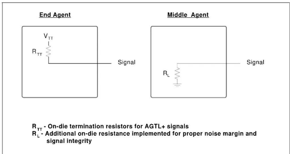
Most Dual-Core Intel Xeon processor 7000 series FSB signals use Assisted Gunning Transceiver Logic (AGTL+) signaling technology. The termination voltage level for the Dual-Core Intel Xeon processor 7000 series AGTL+ signals is V_TT .
Termination resistors are provided on the processor silicon and are terminated to V_TT . Intel chipsets also provide on-die termination, thus eliminating the need to terminate the bus on the system board for most AGTL+ signals. Some AGTL+ signals do not include on-die termination and must be terminated on the system board.
When designing a system, Intel strongly recommends that design teams perform analog simulations of the FSB. Design guidelines for the Dual-Core Intel Xeon processor 7000 series FSB are detailed in the appropriate platform design guide.
Some Dual-Core Intel Xeon processor 7000 series signals include additional on-die resistors ( R_L ) to ensure proper noise margin and signal integrity specifications are met—see Table 2-5 for a list of these signals. Figure 2-1 illustrates the active on-die termination. Signal listings are included in Table 2-5 and Table 2-6.
Figure 2-1. On-Die Front Side Bus Termination
2.1.1 Front Side Bus Clock and Processor Clocking
BCLK[1:0] directly controls the FSB interface speed as well as the core frequency of the processor. As in previous processor generations, the Dual-Core Intel Xeon processor 7000 series core frequency is a multiple of the BCLK[1:0] frequency. The processor bus ratio multiplier will be set during manufacturing.
The BCLK[1:0] inputs directly control the operating speed for the FSB interface. The processor core frequency is configured during reset by using values stored internally during manufacturing. The stored value sets the highest bus fraction at which the particular processor can operate. If lower speeds are desired, the appropriate ratio can be configured by setting bits [15:8] of the IA32_FLEX_BRVID_SEL_MSR.
Clock multiplying within the processor is provided by the internal phase locked loop (PLL), which requires a constant frequency BCLK[1:0] input, with exceptions for spread spectrum clocking. Processor DC and AC specifications for the BCLK[1:0] inputs are provided in Table 2-11. The Dual-Core Intel Xeon processor 7000 series utilizes differential clocks. Details regarding BCLK[1:0] driver specifications are provided in the CK409 Clock Synthesizer/Driver Design Guidelines or CK409B Clock Synthesizer/Driver Design Guidelines. Table 2-1 contains core frequency to FSB multipliers and their corresponding core frequencies.
Table 2-1. Core Frequency to Front Side Bus Multiplier Configuration
| Core Frequency to Front Side Bus Multiplier | Core Frequency with 166 MHz Front Side Bus Clock | Notes |
| 1/14 RESERVED | 1, 2, 3 | |
| 1/15 RESERVED | 2, 3 | |
| 1/16 2.66 GHz | 2, 3 | |
| 1/17 RESERVED | 2, 3 | |
| 1/18 3 GHz | 2, 3 |
NOTES:
- Individual processors operate only at or below the frequency marked on the package.
- Listed frequencies are not necessarily committed production frequencies.
- For valid core frequencies of the processor, refer to the Dual-Core Intel ^® Xeon ^® Processor 7000 Sequence Specification Update.
2.1.2 Front Side Bus Clock Select (BSEL[1:0])
The BSEL[1:0] signals are hardwired outputs used to select the frequency of the processor input clock (BCLK[1:0]). Table 2-2 defines the possible combinations of the signals and the frequency associated with each combination. The required frequency is determined by the processor, chipset, and clock synthesizer. All processors must operate at the same FSB frequency.
The Dual-Core Intel Xeon processor 7000 series operates at 667 MHz FSB frequency (selected by a 166 MHz BCLK[1:0] frequency, respectively). Individual processors operate at the FSB frequency specified by BSEL[1:0].
For more information about these pins, refer to Section 5.1 and the appropriate platform design guide.
Table 2-2. BSEL[1:0] Frequency Table for BCLK[1:0]
| BSEL1 BSEL0 Function | |
| 0 0 RESERVED | |
| 0 1 RESERVED | |
| 1 0 RESERVED | |
| 1 1 166 MHz |
2.1.3 Phase Lock Loop (PLL) Power and Filter
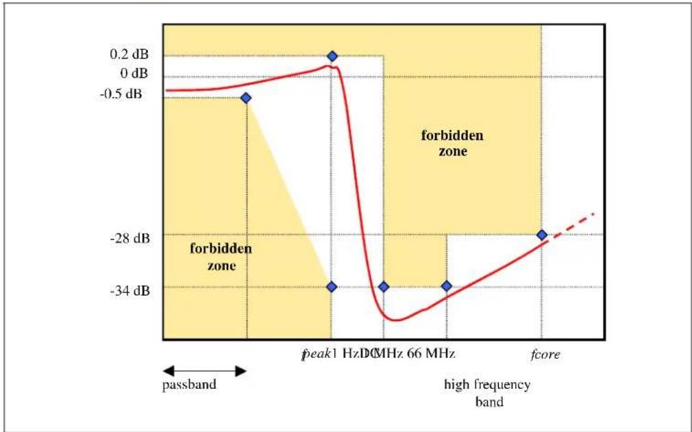
V_CCA , V_CCIOPLL are power sources required by the PLL clock generators on the Dual-Core Intel Xeon processor 7000 series. These are analog PLLs and they require low noise power supplies for minimum jitter. These supplies must be low pass filtered from V_TT .
The AC low-pass requirements, with input at V_TT , are as follows:
- < 0.2 dB gain in pass band
• < 0.5 dB attenuation in pass band < 1 Hz
• > 34 dB attenuation from 1 MHz to 66 MHz -
28 dB attenuation from 66 MHz to core frequency
The filter requirements are illustrated in Figure 2-2. For recommendations on implementing the filter, refer to the appropriate platform design guide.
Figure 2-2. Phase Lock Loop (PLL) Filter Requirements
line
| Frequency Band | Value | | -------------- | --------- | | passband | -0.5 dB | | peak1 | 0.2 dB | | 66 MHz | -34 dB | | fcore | -28 dB |NOTES:
- Diagram not to scale.
- No specification for frequencies beyond f_core (core frequency).
- f_peak , if existent, should be less than 0.05 MHz.
- f_core represents the maximum care frequency supported by the platform.
2.2 Voltage Identification (VID)
The VID[5:0] pins supply the encodings that determine the voltage to be supplied by the V_CC (the core voltage for the Dual-Core Intel Xeon processor 7000 series) voltage regulator. The VID specification for the Dual-Core Intel Xeon processor 7000 series is defined by the Vcc Voltage Regulator Module (VRM) and Enterprise Voltage Regulator-Down (EVRD) 10.2 Design Guidelines. The voltage set by the VID pins is the maximum V_CC voltage allowed by the
processor. A minimum V_CC voltage is provided in Table 2-7 and changes with frequency. This allows processors running at a higher frequency to have a relaxed minimum V_CC voltage specification. The specifications have been set such that one voltage regulator can work with all supported frequencies.
Individual processor VID values may be calibrated during manufacturing such that two devices at the same core speed may have different default VID settings. Furthermore, any Dual-Core Intel Xeon processor 7000 series, even those on the same processor FSB, can drive different VID settings during normal operation.
The Dual-Core Intel Xeon processor 7000 series uses six voltage identification pins (VID[5:0]) to support automatic selection of power supply voltages. Table 2-3 specifies the voltage level corresponding to the state of VID[5:0]. A '1' in this table refers to a high voltage level and a '0' refers to a low voltage level. If the processor socket is empty (i.e. when the voltage regulator sees VID[5:0] = 111111 or VID[5:0] = 011111), or the voltage regulation circuit cannot supply the voltage that is requested, the processor's voltage regulator must disable itself. See the Vcc Voltage Regulator Module (VRM) and Enterprise Voltage Regulator-Down (EVRD) 10.2 Design Guidelines for more details.
The Dual-Core Intel Xeon processor 7000 series provides the ability to operate while transitioning to an adjacent VID and its associated processor core voltage ( V_CC ). This will represent a DC shift in the load line. It should be noted that a low-to-high or high-to-low voltage state change may result in as many VID transitions as necessary to reach the target core voltage. Transitions above the specified VID are not permitted. Table 2-8 includes VID step sizes and DC shift ranges.
The VRM or VRD utilized must be capable of regulating its output to the value defined by the new VID. DC specifications for VID transitions are included in Table 2-8 and Table 2-9. Please refer to the Vcc Voltage Regulator Module (VRM) and Enterprise Voltage Regulator-Down (EVRD) 10.2 Design Guidelines for more details.
Power source characteristics must be guaranteed to be stable whenever the supply to the voltage regulator is stable.
Further details and specifications will be included in future revisions of this document.
Table 2-3. Voltage Identification (VID) Definition
| VID5 VID4 VID3 VID2 VID1 VID0 VID (V) | VID5 VID4 VID3 VID2 VID1 VID0 VID (V) | |||||||||||||
| 0 | 0 | 1 | 0 | 1 | 0 | 0 | 0 8 1 | 0 1 03.2125 7 | 5 | |||||
| 1 | 0 | 1 | 0 | 0 | 1 | 0 | 1 8 1 | 0 0 15.2250 0 | 0 | |||||
| 0 | 0 | 1 | 0 | 0 | 1 | 0 | 8 | 6 | 2 | 5 | 0 1 | 1 0 0 1 1.2375 | ||
| 1 | 0 | 1 | 0 | 0 | 0 | 0 | 1 8 1 | 0 0 07.2500 5 | 0 | |||||
| 0 | 0 | 1 | 0 | 0 | 0 | 0 | 0 8 1 | 0 0 08.2625 7 | 5 | |||||
| 1 | 0 | 0 | 1 | 1 | 1 | 0 | 9 | 0 | 0 | 0 | 1 1 | 0 1 1 1 1.2750 | ||
| 0 | 0 | 0 | 1 | 1 | 1 | 0 | 0 9 0 | 1 1 11.2875 2 | 5 | |||||
| 1 | 0 | 0 | 1 | 1 | 0 | 0 | 1 9 0 | 1 1 02.3000 5 | 0 | |||||
| 0 | 0 | 0 | 1 | 1 | 0 | 0 | 9 | 3 | 7 | 5 | 0 1 | 0 1 1 0 1.3125 | ||
| 1 | 0 | 0 | 1 | 0 | 1 | 0 | 1 9 0 | 1 0 15.3250 0 | 0 | |||||
| 0 | 0 | 0 | 1 | 0 | 1 | 0 | 0 9 0 | 1 0 16.3375 2 | 5 | |||||
| 1 | 0 | 0 | 1 | 0 | 0 | 0 | 1 9 0 | 1 0 07.3500 5 | 0 | |||||
| 0 | 0 | 0 | 1 | 0 | 0 | 0 | 9 | 8 | 7 | 5 | 0 1 | 0 1 0 0 1.3625 | ||
| 1 | 0 | 0 | 0 | 1 | 1 | 1 | 1 0 0 | 0 1 10.3750 0 | 0 | |||||
| 0 | 0 | 0 | 0 | 1 | 1 | 1 | 0 0 0 | 0 1 11.3875 2 | 5 | |||||
| 1 | 0 | 0 | 0 | 1 | 0 | 1 | 0 | 2 | 5 | 0 | 1 1 | 0 0 1 0 1.4000 | ||
| 0 | 0 | 0 | 0 | 1 | 0 | 1 | 0 0 0 | 0 1 03.4125 7 | 5 | |||||
| 1 | 0 | 0 | 0 | 0 | 1 | 1 | 1 0 0 | 0 0 15.4250 0 | 0 | |||||
| 0 | 0 | 0 | 0 | 0 | 1 | 1 | 0 | 6 | 2 | 5 | 0 1 | 0 0 0 1 1.4375 | ||
| 1 | 0 | 0 | 0 | 0 | 0 | 1 | 1 0 0 | 0 0 07.4500 5 | 0 | |||||
| 0 | 0 | 0 | 0 | 0 | 0 | 1 | 0 0 0 | 0 0 08.4625 7 | 5 | |||||
| 1 | 1 | 1 | 1 | 1 | 1 | V | R | M | 0 | f | 1 | 0 1 1 1 | 1 1.4750 | |
| 0 | 1 | 1 | 1 | 1 | 1 | V | R | 0 0 0 | 1 1 1 1.4875 | f | ||||
| 1 | 1 | 1 | 1 | 1 | 0 | 1 | 1 0 1 | 1 1 00.5000 0 | 0 | |||||
| 0 | 1 | 1 | 1 | 1 | 0 | 1 | 0 1 1 | 1 1 02.5125 5 | ||||||
| 1 | 1 | 1 | 1 | 0 | 1 | 1 | 1 0 1 | 1 0 12.5250 5 | 0 | |||||
| 0 | 1 | 1 | 1 | 0 | 1 | 1 | 0 0 1 | 1 0 13.5375 7 | 5 | |||||
| 1 | 1 | 1 | 1 | 0 | 0 | 1 | 1 0 1 | 1 0 05.5500 0 | 0 | |||||
| 0 | 1 | 1 | 1 | 0 | 0 | 1 | 0 0 1 | 1 0 06.5625 2 | 5 | |||||
| 1 | 1 | 1 | 0 | 1 | 1 | 1 | 1 0 1 | 0 1 17.5750 5 | 0 | |||||
| 0 | 1 | 1 | 0 | 1 | 1 | 1 | 0 0 1 | 0 1 18.5875 7 | 5 | |||||
| 1 | 1 | 1 | 0 | 1 | 0 | 1 | 1 0 1 | 0 1 00.6000 0 | 0 | |||||
2.3 Reserved, Unused, and TESTHI Pins
All RESERVED pins must be left unconnected. Connection of these pins to V_CC , V_SS , or to any other signal (including each other) can result in component malfunction or incompatibility with future processors. See Section 5 for a pin listing for the processor and the location of all RESERVED pins.
For reliable operation, always terminate unused inputs or bidirectional signals to their respective deasserted states. On-die termination has been included on the Dual-Core Intel Xeon processor 7000 series to allow signals to be terminated within the processor silicon. Most unused AGTL+ inputs may be left as no-connects since AGTL+ termination is provided on the processor silicon. See Table 2-5 for details on AGTL+ signals that do not include on-die termination. Unused active-high inputs should be connected through a resistor to ground ( V_SS ). Unused outputs may be left unconnected. However, this may interfere with some TAP functions, complicate debug probing, and prevent boundary scan testing. A resistor must be used when tying bidirectional signals to power or ground. When tying any signal to power or ground, a resistor will also allow for system testability. For unused AGTL+ input or I/O signals, use pull-up resistors of the same value as the on-die termination resistors ( R_TT ). See Table 2-15.
TAP, Asynchronous GTL+ inputs, and Asynchronous GTL+ outputs do not include on-die termination. Inputs and utilized outputs must be terminated on the baseboard. Unused outputs may be terminated on the baseboard or left unconnected. Note that leaving unused outputs unterminated may interfere with some TAP functions, complicate debug probing, and prevent boundary scan testing. Signal termination for these signal types is discussed in the appropriate platform design guidelines.
Don't Care pins are pins on the processor package that are not connected to the processor die. These pins can be connected on the motherboard in any way necessary for compatible motherboard designs to support other processor versions.
The TESTHI pins should be tied to V_TT using a matched resistor, where a matched resistor has a resistance value within ±20% of the impedance of the board transmission line traces. For example, if the trace impedance is 50 , then a value between 40 and 60 is required.
The TESTHI pins may use individual pull-up resistors or be grouped together as detailed below. Please note that utilization of boundary scan test will not be functional if pins are connected together. A matched resistor should be used for each group:
- TESTHI[3:0]
- TESTHI[6:5]
- TESTHI4 — cannot be grouped with other TESTHI signals
2.4 Mixing Processors
Intel supports and validates multi-processor configurations in which all processors operate with the same FSB frequency and internal cache sizes. Intel does not support or validate operation of processors with different cache sizes or mixed processor models. Mixing different processor steppings but the same model is supported. Details on this process are provided in the Dual-Core Intel® Xeon® Processor 7000 Sequence Specification Update, Prescott, Nocona and Potomac Processor BIOS Writer's Guide (BWG) document and the AP-485 Intel® Processor Identification and the CPUID Instruction application note.
2.5 Front Side Bus Signal Groups
The FSB signals are grouped by buffer type as listed in Table 2-4. The buffer type indicates which AC and DC specifications apply to the signals. AGTL+ input signals have differential input buffers that use GTLREF as a reference level. In this document, the term “AGTL+ Input” refers to the AGTL+ input group as well as the AGTL+ I/O group when receiving. Similarly, “AGTL+ Output” refers to the AGTL+ output group as well as the AGTL+ I/O group when driving.
Implementing a source synchronous data bus requires specifying two sets of timing parameters. One set is for common clock signals which are dependent upon the rising edge of BCLK0 (ADS#, HIT#, HITM#, etc.). The second set is for the source synchronous signals that are relative to their respective strobe lines (data and address) as well as the rising edge of BCLK0. Asynchronous signals are present (A20M#, IGNNE#, etc.) and can become active at any time during the clock cycle. Table 2-4 identifies signals as common clock, source synchronous, and asynchronous.
Table 2-4. Front Side Bus Pin Groups
| Signal Group Type Signals | 1 | ||
| AGTL+ Common Clock Input Syncronous to BCLK[1:0] BPRI#, | DEFER#, RESET#, RS[2:0]#, RSP#, TRDY# | ||
| AGTL+ Common Clock I/O Syncronous to BCLK[1:0] ADS#, AP | [1:0]#, BINIT#, BNR#, BPM[5:0]#, BR[3:0]#, DBSY#, DP[3:0]#, DRDY#, HIT#, HITM#, LOCK#, MCERR# | ||
| AGTL+ Source Synchronous I/O Synchronous to associated strobe | |||
| Signals | Associated Strobe | ||
| REQ[4:0]#, A[37:36,16:3]# | ADSTB0# | ||
| A[39:38,35:17]# | ADSTB1# | ||
| D[15:0]#, DBI0# | DSTBP0#, DSTBN0# | ||
| D[31:16]#, DBI1# | DSTBP1#, DSTBN1# | ||
| D[47:32]#, DBI2# | DSTBP2#, DSTBN2# | ||
| D[63:48]#, DBI3# | DSTBP3#, DSTBN3# | ||
| AGTL+ Strobe Input/Output | Synchronous to BCLK[1:0] ADSTB[1:0]#, DSTBP[3:0]#, DSTBN[3:0]# | ||
| AGTL+ Asynchronous Output | Asynchronous | FERR#/PBE#, IERR#, PROCHOT#, | |
| GTL+ Asynchronous Input | Asynchronous | A20M#, FORCEPR#, IGNNE#, INIT#, LINT0/INTR, LINT1/NMI, SMI#, STPCLK# | |
| GTL+ Asynchronous Output | Asynchronous | THERMTRIP# | |
| TAP Input | Synchronous to TCK | TCK, TDI, TMS | |
| TAP Input | Asynchronous | TRST# | |
| TAP Output | Synchronous to TCK | TDO | |
| Front Side Bus Clock Input | Clock | BCLK[1:0] | |
| SMBus | Synchronous to SM_CLK | SM_ALERT#, SM_CLK, SM_DAT, SM_EP_A[2:0], SM_TS_A[1:0], SM_WP | |
| Power/Other | Power/Other | BOOT_SELECT, BSEL[1:0], COMP0, TESTHI[6:0], GTLREF[3:0], ODTEN, PWRGOOD, RESERVED, SKTOCC#, SLEW_CTRL, SM_VCC, TEST_BUS, VCC, VCCA, VCCIOPPLL, VCCSENSE, VID[5:0], VIDPWRGD, VSS, VSSA, VSSSENSE, VTT, VTTEN, PROCTYPE | |
NOTES:
1. Refer to Section 5.1 for signal descriptions.
Table 2-5. Signal Description Table
| Signals with R_TT^1 |
| A[39:3]#, ADS#, ADSTB[1:0]#, AP[1:0]#, BINIT#, BNR#, BOOT_SELECT2, BPRI#, D[63:0]#, DBI[3:0]#, DBSY#, DEFER#, DP[3:0]#, DRDY#, DSTBN[3:0]#, DSTBP[3:0]#, FORCEPR#, HIT#, HITM#, LOCK#, MCERR#, ODTEN3, REQ[4:0]#, RS[2:0]#, TEST_BUS, RSP#, TCK4, TDI4, TMS4, TRDY#, TRST#4 |
| Signals with R_L |
| BINIT#, BNR#, HIT#, HITM#, MCERR# |
NOTES:
- Signals not included in the "Signals with R_TT " list require termination on the baseboard. Please refer to Table 2-4 for the signal type and Table 2-12 to Table 2-17 for the corresponding DC specifications.
- The BOOT_SELECT pin is not terminated with R_TT . It has a 250-5000 Ω internal pullup.
- THE ODTEN pin is not terminated with R_TT . It has a 2 KΩ -10 KΩ internal pullup.
- TCK, TDI, TMS and TRST# are not terminated with R_TT . They have a 4 KΩ-20 KΩ internal pullup.
The ODTEN signals enables or disables R_TT . Those signals affected by ODTEN still present R_TT termination to the signal's pin when the processor is placed in tri-state mode.
Furthermore, the following signals are not affected when the processor is placed in tri-state mode: BSEL[1:0], SKTOCC#, SM_ALERT#, SM_CLK, SM_DAT, SM_EP_A[2:0], SM_TS_A[1:0], SM_WP, TEST_BUS, TESTHI[6:0], VID[5:0], TDO and VTTEN.
Table 2-6. Signal Reference Voltages
| GTLREF V | ^1/2 |
| A20M#, A[39:3]#, ADS#, ADSTB[1:0]#, AP[1:0]#, BINIT#, BNR#, BPM[5:0]#, BPRI#, BR[3:0]#, D[63:0]#, DBI[3:0]#, DBSY#, DEFER#, DP[3:0]#, DRDY#, DSTBN[3:0]#, DSTBP[3:0]#, FORCEPR#, HIT#, HITM#, IGNNE#, INIT#, LINT0/INTR, LINT1/NMI, LOCK#, MCERR#, ODTEN, REQ[4:0]#, RESET#, RS[2:0]#, RSP#, SMI#, STPCLK#, TRDY# | BOOT_SELECT, PWRGOOD ^1 , TCK ^1 , TDI ^1 , TMS ^1 , TRST ^1 , VIDPWRGD |
NOTES:
- These signals also have hysteresis added to the reference voltage. See Table 2-15 for more information.
2.6 GTL+ Asynchronous Signals and AGTL + Asynchronous Signals
The Dual-Core Intel Xeon processor 7000 series does not utilize CMOS voltage levels on any signals that connect to the processor silicon. As a result, input signals such as A20M#, FORCEPR#, IGNNE#, INIT#, LINT0/INTR, LINT1/NMI, SMI#, SLP#, and STPCLK# utilize GTL input buffers. Legacy output THERMTRIP# utilizes a GTL+ output buffers. All of these Asynchronous GTL+ signals follow the same DC requirements as GTL+ signals, however the outputs are not driven high (during the logical 0-to-1 transition) by the processor. FERR#/PBE#, IERR#, and IGNNE# have now been defined as AGTL+ asynchronous signals as they include an active p-MOS device. GTL+ asynchronous and AGTL+ asynchronous signals do not have setup or hold time specifications in relation to BCLK[1:0]. However, all of the GTL+ asynchronous and AGTL+ asynchronous signals are required to be asserted/deasserted for at least six BCLKs in order for the processor to recognize them. See Table 2-16 for the DC specifications for the asynchronous GTL+ signal groups.
2.7 Test Access Port (TAP) Connection
Due to the voltage levels supported by other components in the TAP logic, Intel recommends that the Dual-Core Intel Xeon processor 7000 series be first in the TAP chain, followed by any other components within the system. Use of a translation buffer to connect to the rest of the chain is recommended unless one of the other components is capable of accepting an input of the appropriate voltage. Similar considerations must be made for TCK, TMS, TRST#, TDI, and TDO. Two copies of each signal may be required, each driving a different voltage level.
2.8 Absolute Maximum and Minimum Ratings
Table 2-7 specifies absolute maximum and minimum ratings. Within functional operation limits, functionality and long-term reliability can be expected.
At conditions outside functional operation condition limits, but within absolute maximum and minimum ratings, neither functionality nor long-term reliability can be expected. If a device is returned to conditions within functional operation limits after having been subjected to conditions outside these limits, but within the absolute maximum and minimum ratings, the device may be functional, but with its lifetime degraded depending on exposure to conditions exceeding the functional operation condition limits.
At conditions exceeding absolute maximum and minimum ratings, neither functionality nor long-term reliability can be expected. Moreover, if a device is subjected to these conditions for any length of time then, when returned to conditions within the functional operating condition limits, it will either not function, or its reliability will be severely degraded.
Although the processor contains protective circuitry to resist damage from static electric discharge, precautions should always be taken to avoid high static voltages or electric fields.
Table 2-7. Processor Absolute Maximum Ratings
| Symbol | Parameter Min Max Unit Notes | 1, 2 | |||
| V_CC | Processor core supply voltage with respect to V_SS | -0.3 1.55 V | |||
| V_TT | Front side bus termination voltage with respect to V_SS | -0.3 1.55 V | |||
| T_CASE | Processor case temperature | See Section 6 | See Section 6 | °C | |
| T_STORAGE | Processor storage temperature | -40 | 85 | °C | 3, 4 |
NOTES:
- For functional operation, all processor electrical, signal quality, mechanical, and thermal specifications must be satisfied.
- Overshoot and undershoot voltage guidelines for input, output, and I/O signals are outlined in Table 2-11. Excessive overshoot or undershoot on any signal will likely result in permanent damage to the processor.
- Storage temperature is applicable to storage conditions only. In this scenario, the processor must not receive a clock, and no pins can be connected to a voltage bias. Storage within these limits will not affect the long-term reliability of the device. For functional operation, please refer to the processor case temperature specifications.
- This rating applies to the processor and does not include any packaging or trays.
2.9 Processor DC Specifications
The following notes apply:
- The processor DC specifications in this section are defined at the processor core silicon and not at the package pins unless noted otherwise.
- The notes associated with each parameter are part of the specification for that parameter.
- Unless otherwise noted, all specifications in the tables apply to all frequencies and cache sizes.
See Section 5 for the pin signal definitions. Most of the signals on the processor FSB are in the AGTL+ signal group. The DC specifications for these signals are listed in Table 2-14.
Table 2-8 lists the DC specifications for the Dual-Core Intel Xeon processor 7000 series and are valid only while meeting specifications for case temperature, clock frequency, and input voltages.
2.9.1 Flexible Motherboard (FMB) Guidelines
The FMB guidelines are estimates of the maximum values that the Dual-Core Intel Xeon processor 7000 series will reach over the product lifetime. The values are only estimates as actual specifications for future processors may differ. The Dual-Core Intel Xeon processor 7000 series may or may not have specifications equal to the FMB value in the foreseeable future. System designers should meet the FMB values to ensure that their systems will be compatible with future releases of the Dual-Core Intel Xeon processor 7000 series.
Table 2-8. Voltage and Current Specifications (Sheet 1 of 2)
| Symbol Parameter Min Typ Max | Unit Notes | 1 | ||||
| VID range | VID range for Dual-Core Intel Xeon processor 7000 series | 1.2625 | 1.4125 | V | 2,3 | |
| V_CC | V_CC for Dual-Core Intel Xeon processor 7000 series | See Table 2-9 and Figure 2-4 | VID - I_CC (max) * 1.25 mΩ | V | 3,4,5,6,7 | |
| VID Transition | VID step size during a transition | ±12.5 | mV | 8 | ||
| Total allowable DC load line shift from VID steps | 450 | mV | 9 | |||
| V_TT | Front side bus termination voltage (DC specification) | 1.176 | 1.20 | 1.224 | V | 10 |
| Front side bus termination voltage (AC & DC specification) | 1.140 | 1.20 | 1.260 | V | 10,11 | |
| SM_VCC | SMBus supply voltage | 3.135 | 3.300 | 3.465 | V | 12 |
| I_CC | I_CC for Dual-Core Intel Xeon processor 7000 series with multiple VIDs | 150 (FMB) A | 6,7,13 | |||
| I_TT | Front Side Bus end-agent V_TT current | 4 | A | 14 | ||
| I_TT | Front Side Bus mid-agent V_TT current | 1.3 | A | 12 | ||
| I_SM\_VCC | I_CC for SMBus supply | 100 | 122.5 | mA | 11 | |
| I_CC\_VCCA | I_CC for PLL power pins | 60 | mA | 15 | ||
| I_CC\_VCCIOPLL | I_CC for I/O PLL power pins | 60 | mA | 15 | ||
| I_CC\_GTLREF | I_CC for GTLREF pins | 200 | μA | 16 | ||
| I_SGNT | I_CC Stop Grant for Dual-Core Intel Xeon processor 7000 series 2.8 GHz - FMB | 63 | A | 7,17,18 | ||
| I_TCC | I_CC TCC Active | I_CC | A | 19 | ||
Table 2-8. Voltage and Current Specifications (Sheet 2 of 2)
| Symbol Parameter Min Typ Max Unit Notes | 1 | |||||
| I_CC\_TDC | I_CC for Dual-Core Intel Xeon processor 7000 series Thermal Design Current 2.8 - FMB GHz | 130 A | 7, 20, 13 | |||
NOTES:
- Unless otherwise noted, all specifications in this table apply to all processors. These specifications are based on silicon characterization, however they may be updated as further data becomes available.
- Individual processor VID values may be calibrated during manufacturing such that two devices at the same speed may have different VID settings.
- These voltages are targets only. A variable voltage source should exist on systems in the event that a different voltage is required. See Section 2.2 for more information.
- The voltage specification requirements are measured across vias on the platform for the VCCSENSE and VSSSENSE pins close to the socket with a 100 MHz bandwidth oscilloscope, 1.5 pF maximum probe capacitance, and 1 MΩ minimum impedance. The maximum length of ground wire on the probe should be less than 5 mm. Ensure external noise from the system is not coupled in the scope probe.
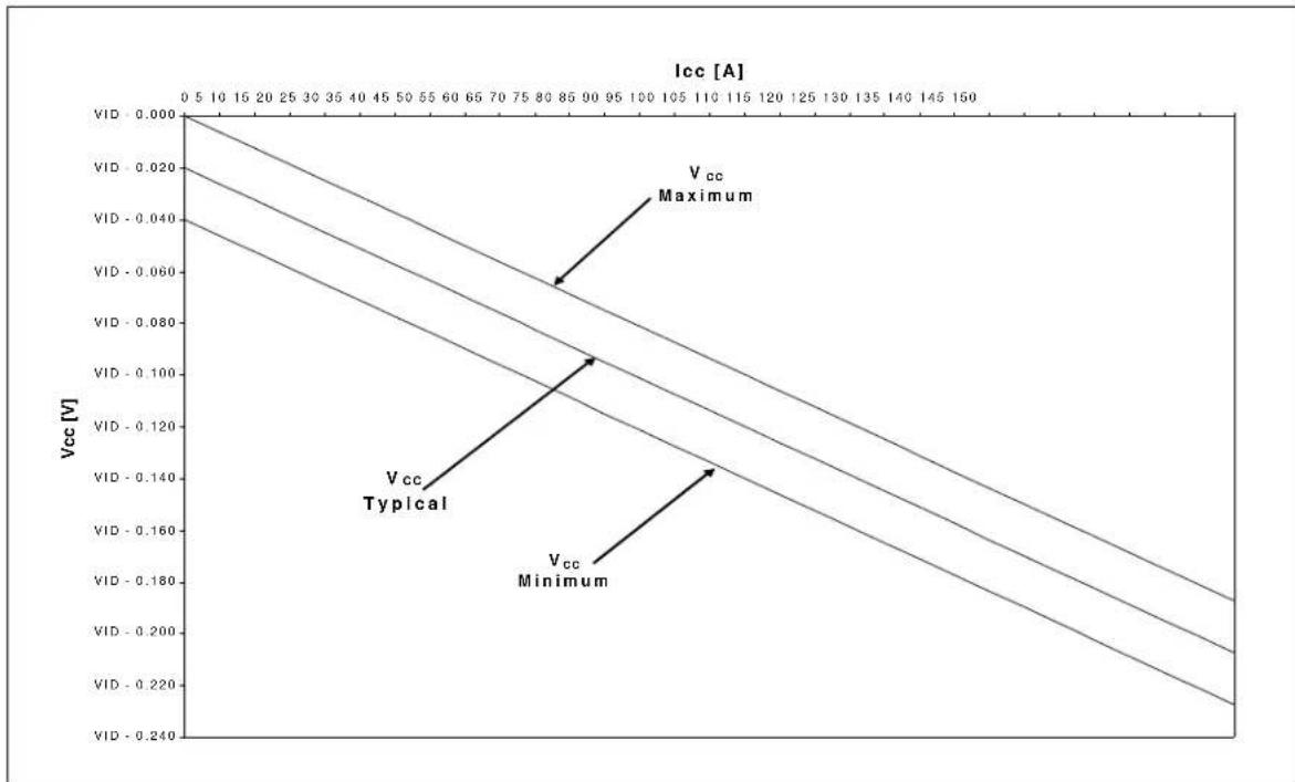
- Refer to Table 2-9 and corresponding Figure 2-4. The processor should not be subjected to any static V_CC level that exceeds the V_CC_MAX associated with any particular current. Failure to adhere to this specification can shorten processor lifetime.
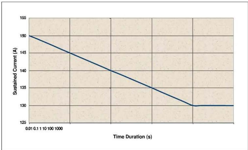
- Minimum V_CC and maximum I_CC are specified at the maximum processor case temperature ( T_CASE ) shown in Table 6-1. I_CC_MAX is specified at the relative V_CC_MAX point on the V_CC load line. The processor is capable of drawing I_CC_MAX for up to 10 ms. Refer to Figure 2-3 for further details on the average processor current draw over various time durations.
- FMB is the flexible motherboard guideline. These guidelines are for estimation purposes only. See Section 2.9.1 for further details on FMB guidelines.
- This specification represents the V_CC reduction due to each VID transition. See Section 2.2. AC timing requirements will be included in future revisions of this document.
- This specification refers to the potential total reduction of the load line due to VID transitions below the specified VID.
- V_TT must be provided via a separate voltage source and must not be connected to V_CC . This specification is measured at the pin.
- Baseboard bandwidth is limited to 20 MHz.
- This specification refers to a single processor with R_TT disabled. Please note the end agent and middle agent may not require I_TT(max) simultaneously. Details will be provided in future revisions of this document.
- This specification refers to platforms implementing a power delivery system that complies with VR 10.2 guidelines. Please see the Voltage Regulator Module (VRM) and Enterprise Voltage Regulator-Down (EVRD) 10.2 Design Guidelines for further details.
- This specification refers to a single processor with R_TT enabled. Please note the end agent and middle agent may not require I_TT() simultaneously. This parameter is based on design characterization and not tested.
- These specifications apply to the PLL power pins VCCA, VCCIOPLL, and VSSA. See Section 2.1.3 for details. These parameters are based on design characterization and are not tested.
- This specification represents a total current for all GTLREF pins.
- The current specified is also for HALT State.
- This specification applies to both the HALT and Enhanced HALT States.
- The maximum instantaneous current the processor will draw while the thermal control circuit is active as indicated by the assertion of the PROCHOT# signal is the maximum I_CC for the processor.
- I_CC_TDC (Thermal Design Current) is the sustained (DC equivalent) current that the processor is capable of drawing indefinitely and should be used for the voltage regulator temperature assessment. The voltage regulator is responsible for monitoring its temperature and asserting the necessary signal to inform the processor of a thermal excursion. Please see the applicable design guidelines for further details. The processor is capable of drawing I_CC_TDC indefinitely. Refer to Figure 2-3 for further details on the average processor current draw over various time durations. This parameter is based on design characterization and is not tested.
Figure 2-3. Dual-Core Intel® Xeon® Processor 7000 SeriesLoad Current vs. Time
line
| Time Duration (s) | Sustained Current (A) | | ----------------- | --------------------- | | 0.01 | 150 | | 0.1 | 145 | | 1 | 140 | | 10 | 135 | | 100 | 130 | | 1000 | 130 |NOTES:
- Processor or voltage regulator thermal protection circuitry should not trip for load currents greater than I_CC TDC.
- Not 100% tested. Specified by design characterization.
Table 2-9. V_CC Static and Transient Tolerance
| Icc Vcc_max | Vcc_typical Vcc_min Notes | ||
| 0 VID-0.000 | VID-0.020 VID-0.040 1,2,3 | ||
| 5 VID-0.006 | VID-0.026 VID-0.046 1,2,3 | ||
| 10 VID-0.013 | VID-0.033 VID-0.052 1,2,3 | ||
| 15 VID-0.019 | VID-0.039 VID-0.059 1,2,3 | ||
| 20 VID-0.025 | VID-0.045 VID-0.065 1,2,3 | ||
| 25 VID-0.031 | VID-0.051 VID-0.071 1,2,3 | ||
| 30 VID-0.038 | VID-0.058 VID-0.077 1,2,3 | ||
| 35 VID-0.044 | VID-0.064 VID-0.084 1,2,3 | ||
| 40 VID-0.050 | VID-0.070 VID-0.090 1,2,3 | ||
| 45 VID-0.056 | VID-0.076 VID-0.096 1,2,3 | ||
| 50 VID-0.063 | VID-0.083 VID-0.103 1,2,3 | ||
| 55 VID-0.069 | VID-0.089 VID-0.109 1,2,3 | ||
| 60 VID-0.075 | VID-0.095 VID-0.115 1,2,3 | ||
| 65 VID-0.081 | VID-0.101 VID-0.121 1,2,3 | ||
| 70 VID-0.087 | VID-0.108 VID-0.128 1,2,3 | ||
| 75 VID-0.094 | VID-0.114 VID-0.134 1,2,3 | ||
| 80 VID-0.100 | VID-0.120 VID-0.140 1,2,3 | ||
| 85 VID-0.106 | VID-0.126 VID-0.147 1,2,3 | ||
| 90 VID-0.112 | VID-0.133 VID-0.153 1,2,3 | ||
| 95 VID-0.119 | VID-0.139 VID-0.159 1,2,3 | ||
| 100 | VID-0.125 VID-0.145 VID-0.165 1,2,3 | ||
| 105 | VID-0.131 VID-0.151 VID-0.172 1,2,3 | ||
| 110 | VID-0.137 VID-0.158 VID-0.178 1,2,3 | ||
| 115 | VID-0.144 VID-0.164 VID-0.184 1,2,3 | ||
| 120 | VID-0.150 VID-0.170 VID-0.190 1,2,3 | ||
| 125 | VID-0.156 VID-0.177 VID-0.197 1,2,3 | ||
| 130 | VID-0.162 VID-0.183 VID-0.203 1,2,3 | ||
| 135 | VID-0.169 VID-0.189 VID-0.209 1,2,3 | ||
| 140 | VID-0.175 VID-0.195 VID-0.216 1,2,3 | ||
| 145 | VID-0.181 VID-0.202 VID-0.222 1,2,3 | ||
| 150 | VID-0.187 VID-0.208 VID-0.228 1,2,3 |
NOTES:
- The V_CC MIN and V_CC MAX loadlines represent static and transient limits.
- This table is intended to aid in reading discrete points on Figure 2-4.
- The loadlines specify voltage limits at the die measured at the VCCSENSE and VSSSENCE pins. Voltage regulation feedback for voltage regulator circuits must be taken from processor V_CC and V_SS pins. Refer to the Voltage Regulator Module (VRM) and Enterprise Voltage Regulator Down (ERVD) 10.2 Design Guidelines for socket loadline guidelines and VR implementation.
Figure 2-4. V _CC Static and Transient Tolerance
line
| Icc [A] | Vcc [V] | | ------- | ------- | | 0 | 0.000 | | 5 | 0.020 | | 10 | 0.040 | | 15 | 0.060 | | 20 | 0.080 | | 25 | 0.100 | | 30 | 0.120 | | 35 | 0.140 | | 40 | 0.160 | | 45 | 0.180 | | 50 | 0.200 | | 55 | 0.220 | | 60 | 0.240 |NOTES:
- The V_CC MIN and V_CC MAX loadlines represent static and transient limits.
- The V_CC_MIN and V_CC_MAX loadlines are plots of the discrete point found in Table 2-9.
- Refer to Table 2-8 for processor VID information.
- The loadlines specify voltage limits at the die measured at the VCCSENSE and VSSSENSE pins. Voltage regulation feedback for voltage regulator circuits must be taken from processor V_CC and V_SS pins. Refer to the Voltage Regulator Module (VRM) and Enterprise Voltage Regulator-Down (EVRD) 10.2 Design Guidelines for socket loadline guidelines and VR implementation.
2.9.2 Vcc Overshoot Specification
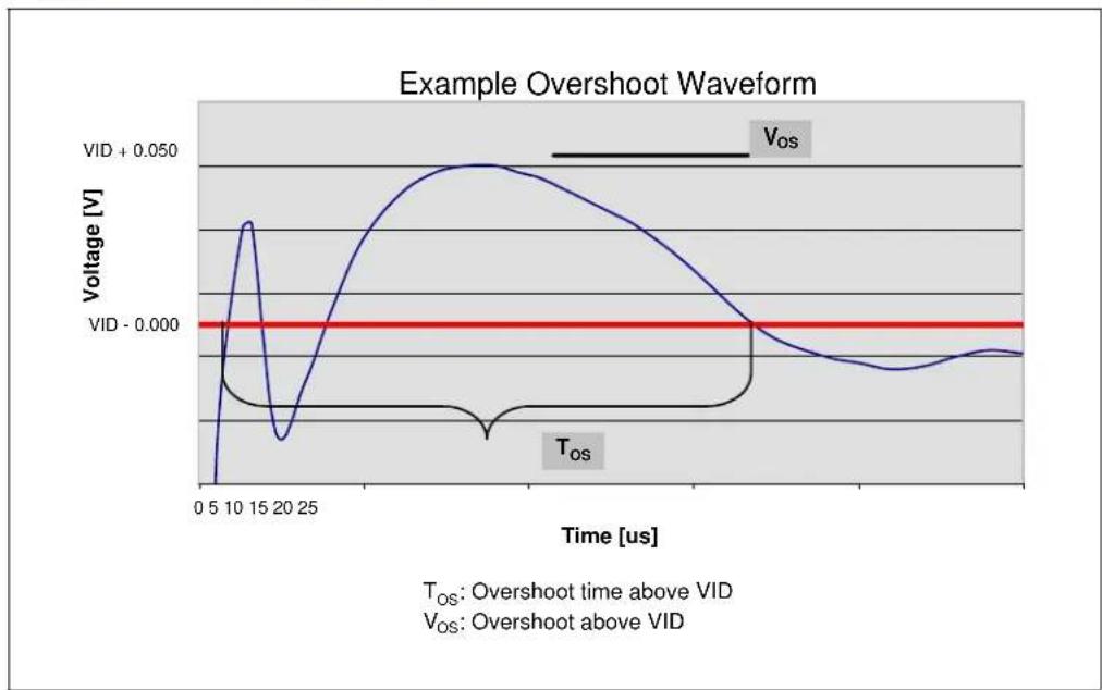
The Dual-Core Intel Xeon processor 7000 series processor can tolerate short transient overshoot events where V_CC exceeds the VID voltage when transitioning from a high-to-low current load condition. This overshoot cannot exceed VID + V_OS_MAX . ( V_OS_MAX is the maximum allowable overshoot above VID). These specifications apply to the processor die voltage as measured across the VCCSENSE and VSSSENSE pins.
Table 2-10. V_CC Overshoot Specifications
| Symbol | Parameter | Min | Max | Units | Figure | Notes |
| V_OS\_MAX | Magnitude of V_CC overshoot above VID | 0.050 | V | 2-5 | ||
| T_OS\_MAX | Time duration of V_CC overshoot above VID | 25 | μs 2-5 |
Figure 2-5. Vcc Overshoot Example Waveform
line
| Time [us] | Voltage [V] | | --------- | ----------- | | 0 | -0.000 | | 5 | 0.000 | | 10 | 0.025 | | 15 | 0.035 | | 20 | 0.010 | | 25 | 0.045 | | 30 | 0.048 | | 35 | 0.042 | | 40 | 0.030 | | 45 | 0.015 | | 50 | 0.005 | | 55 | 0.002 | | 60 | 0.001 | | 65 | 0.000 | | 70 | -0.001 | | 75 | -0.002 | | 80 | -0.003 | | 85 | -0.004 | | 90 | -0.005 | | 95 | -0.006 | | 100 | -0.007 |NOTES:
-
V_OS is measured overshoot voltage.
-
T_OS is measured time duration above VID.
Table 2-11. Front Side Bus Differential BCLK Specifications
| Symbol Parameter Min Typ Max Unit Figure Notes | |||||||
| V_L | Input Low Voltage | -0.150 | 0.000 | N/A | V | ||
| V_H | Input High Voltage | 0.660 | 0.700 | 0.850 | V | ||
| V_CROSS(abs) | Absolute Crossing Point | 0.250 | N/A | 0.550 | V | 1, 2 | |
| V_CROSS(rel) | Relative Crossing Point | 0.250 + 0.5^* (V_Havg - 0.700) | N/A | 0.550 + 0.5^* (V_Havg - 0.700) | V | 3, 2, 4 | |
| V_CROSS | Range of Crossing Point | N/A | N/A | 0.140 | V | ||
| V_OV | Overshoot | N/A | N/A | V_H + 0.300 | V | 5 | |
| V_US | Undershoot | -0.300 | N/A | N/A | V | 6 | |
| V_RBM | Ringback Margin | 0.200 | N/A | N/A | V | 7 | |
| V_TM | Threshold Margin | V_CROSS-0.100 V | C_ROSS+0.100 | V | 8 | ||
NOTES:
-
Crossing voltage is defined as the instantaneous voltage value when the rising edge of BCLK0 is equal to the falling edge of BCLK1.
-
The crossing point must meet the absolute and relative crossing point specifications simultaneously.
-
V_Havg is the statistical average of the V_H measured by the oscilloscope.
-
V_Havg can be measured directly using "Vtop" on Agilent scopes and "High" on Tektronix scopes.
-
Overshoot is defined as the absolute value of the maximum voltage.
-
Undershoot is defined as the absolute value of the minimum voltage.
-
Ringback Margin is defined as the absolute voltage difference between the maximum Rising Edge Ringback and the maximum Falling Edge Ringback.
-
Threshold Region is defined as a region entered around the crossing point voltage in which the differential receiver switches. It includes input threshold hysteresis.
Table 2-12. BSEL[1:0], VID[5:0], and DC Specifications
| Symbol Parameter Max Unit Notes | ||||
| R_ON | Buffer On Resistance 60 Ω | 1 | ||
| I_OL | Max Pin Current 8 mA | |||
| I_LO | Output Leakage Current 200 μA | 2 | ||
| V_TOL | Voltage Tolerance | 3.3 + 5% V | 3 | |
NOTES:
- These parameters are not tested and are based on design simulations.
- Leakage to V_SS with pin held at 2.5 V.
- Represents the maximum allowable termination voltage.
Table 2-13. VIDPWRGD DC Specifications
| Symbol | Parameter | Min | Max | Unit | Figure | Notes |
| V_IL | Input Low Voltage | 0.0 | 0.30 | V | ||
| V_IH | Input High Voltage | 0.90 | V_TT | V |
Table 2-14. AGTL+ Signal Group DC Specifications
| Symbol | Parameter | Min | Max | Unit | Notes |
| V_IL | Input Low Voltage | 0.0 | GTLREF – (0.10 * V_TT ) | V | 1,3 |
| V_IH | Input High Voltage | GTLREF +(0.10 * V_TT ) | V_TT | V | 2,3 |
| V_OH | Output High Voltage | 0.90 * V_TT | V_TT | V | 3 |
| I_OL | Output Low Current | N/A | V_TT /(0.50 * Rtt_min + R_ON\_min R_L ) | mA | 5 |
| I_LI | Input Leakage Current | N/A | ±200 | μA | 4,6 |
| I_LO | Output Leakage Current | N/A | ±200 | μA | 4,6 |
| R_ON | Buffer On Resistance | 4 | 8 | Ω |
NOTES:
- V_ is defined as the voltage range at a receiving agent that will be interpreted as a logical low value.
- V_IH is defined as the voltage range at a receiving agent that will be interpreted as a logical high value.
- The V_TT represented in these specifications refers to instantaneous V_TT
- Leakage to V_SS with pin held at V_TT .
- The maximum output current is based on maximum current handling capability of the buffer and is not specified into the test load
- Leakage to V_TT with pin held at 300 mV
Table 2-15. PWRGOOD Input and TAP Signal Group DC Specifications (Sheet 1 of 2)
| Symbol | Parameter | Min | Max | Unit | Notes |
| V_HYS | Input Hysteresis | 200 | 350 | mV | 5 |
| V_t+ | Input Low to High Threshold Voltage | 0.5 * ( V_TT + V_HYS\_MIN ) | 0.5 * ( V_TT + V_HYS\_MAX ) | V | 3 |
| V_t- | Input High to Low Threshold Voltage | 0.5 * ( V_TT - V_HYS\_MAX ) | 0.5 * ( V_TT - V_HYS\_MIN ) | V | 3 |
| V_OH | Output High Voltage | N/A | V_TT | V | 1,2,4 |
| I_OL | Output Low Current | 45 | mA | 4 | |
| I_IL | Input Leakage Current | N/A | ±200 μA |
Table 2-15. PWRGOOD Input and TAP Signal Group DC Specifications (Sheet 2 of 2)
| Symbol | Parameter | Min | Max | Unit | Notes |
| I_OL | Output Leakage Current N/A | ±200 μA | |||
| R_ON | Buffer On Resistance 48 Ω | ||||
NOTES:
- All outputs are open drain.
- The V_TT represented in these specifications refers to instantaneous V_TT .
- The maximum output current is based on maximum current handling capability of the buffer and is not specified into the test load.
- V_HYS represents the amount of hysteresis, nominally centered about 0.5 × V_TT for all PWRGOOD and TAP inputs.
Table 2-16. GTL+ Asynchronous and AGTL+ Asynchronous Signal Group DC Specifications
| Symbol | Parameter | Min | Max | Unit | Notes1 |
| V_IL | Input Low Voltage | 0.0 | GTLREF – (0.10 * V_TT ) | V | 2, 3 |
| V_IH | Input High Voltage | GTLREF +(0.10 * V_TT ) | V_TT | V | 2, 4 |
| V_OH | Output High Voltage | 0.90 * V_TT | V_TT | V | 2 |
| I_OL | Output Low Current | N/A | 50 | mA | 2, 5 |
| I_LI | Input Leakage Current | N/A | ±200 | μA | 6, 7 |
| I_LO | Output Leakage Current | N/A | ±200 | μA | 6, 7 |
| R_on | Buffer On Resistance | 4 | 8 | Ω |
NOTES:
- Unless otherwise noted, all specifications in this table apply to all processor frequencies.
- The V_TT represented in these specifications refers to instantaneous V_TT .
- V_IL is defined as the voltage range at a receiving agent that will be interpreted as a logical low value.
- V_IH is defined as the voltage range at a receiving agent that will be interpreted as a logical high value.
- Refer to Table 2-5 to determine which signals include additional on-die termination resistance ( R_L ).
- Leakage to V_SS with pin held at V_TT .
- Leakage to V_TT with pin held at 300 mV.
Table 2-17. SMBus Signal Group DC Specifications
| Symbol | Parameter | Min | Max | Unit | Notes 1, 2 |
| V_IL | Input Low Voltage | -0.30 | 0.30 * SM_VCC | V | |
| V_IH | Input High Voltage | 0.70 * SM_VCC | 3.465 | V | |
| V_OL | Output Low Voltage | 0 | 0.400 | V | |
| I_OL | Output Low Current | N/A | 3.0 | mA | |
| I_LI | Input Leakage Current | N/A | ± 10 | μA | |
| I_LO | Output Leakage Current | N/A | ± 10 | μA | |
| C_SMB | SMBus Pin Capacitance | 15.0 | pF | 3 |
NOTES:
- These parameters are based on design characterization and are not tested.
- All DC specifications for the SMBus signal group are measured at the processor pins.
- Platform designers may need this value to calculate the maximum loading of the SMBus and to determine maximum rise and fall times for SMBus signals.
Electrical Specifications
intel®
3 Mechanical Specifications
The Dual-Core Intel Xeon processor 7000 series is packaged in a FC-mPGA4 package that interfaces with the motherboard via a mPGA604 socket. The package consists of a processor core mounted on a substrate pin-carrier. An IHS is attached to the package substrate and core and serves as the mating surface for processor component thermal solutions, such as a heatsink. Figure 3-1 shows a sketch of the processor package components and how they are assembled together. Refer to the mPGA604 Socket Design Guidelines for complete details on the mPGA604 socket.
The package components shown in Figure 3-1 include the following:
- IHS
- Processor die
- FC-mPGA4 package
- Pin-side capacitors
- Package pin
Figure 3-1. Processor Package Assembly Sketch
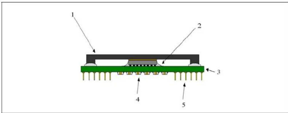
Note: Figure 3-1 is not to scale and is for reference only. The mPGA604 socket is not shown.
3.1 Package Mechanical Drawing
The package mechanical drawings are shown in Figure 3-2 and Figure 3-3. The drawings include dimensions necessary to design a thermal solution for the processor. These dimensions include:
- Package reference with tolerances (total height, length, width, etc.)
- IHS parallelism and tilt
- Pin dimensions
- Top-side and back-side component keepout dimensions
- Reference datums
All drawing dimension are in mm [in].
Figure 3-2. Processor Package Drawing (Sheet 1 of 2)
![D IHS C D2 PACKAGE C IHS LID TOP VIEW SIDE VIEW B1 C1 B2 C2 H1 G1 J2 H2 G2 J1 BOTTOM VIEW A FRONT VIEW B IHS LID IHS SEALANT PACKAGE SUBSTRATE 0.125 [.005] // 0.203 [.008] A 0.65 MAX [.026] F2 2.03±0.08 [.080±.003] Ø1.032 MAX [.041] ØP Ø0.65 MAX [.026] RO.0254-0.0650 [.001-.002] Ø0.37 MAX [.015] DETAIL A SCALE 10:1 A SYMBOL MILLIMETERS [INCHES] COMMENTS MIN MAX B1 53.24 (2.096) 53.44 (2.104) B2 53.24 (2.096) 53.44 (2.104) C1 38.4 (1.512) 38.6 (1.520) C2 38.4 (1.512) 38.6 (1.520) D2 1.27 BASIC (.050) F2 3.665 [.144] 4.101 [.163] G1 38.1 BASIC (.500) G2 30.48 BASIC (.1,200) H1 19.05 BASIC (.750) H2 13.91 BASIC (.550) J1 1.27 BASIC (.050) J2 1.27 BASIC (.050) P 0.28 (.011) 0.33 (.013) DEPARTMENT ATD INTE 2263 WEDER COLLISE MWD P.O. RDE SAB COUP SANTA CLARA CA 93552-8/18 TITLE EMTS DRAWING TITLE MATERIALS: DRAW NO NUMBER REV C 97394 1 TOLER: DO NOT SCALE DRAWING SHEET + OF 2](/content/2026/05/1140870/images/bca1612f6e8a6d6cd9021a12e984fc5a163ad568201659eca63ac8281f439830.jpg)
Figure 3-3. Processor Package Drawing (Sheet 2 of 2)
![D C HG NO C07394 SHT. 2 REV A 6.35 [1.2501] [12.7 [1.5001] [2.7 [1.5001] BOTTOM VIEW 1.5 MAX ALLOWABLE COMPONENT HEIGHT [0.59] SIDE VIEW COMPONENT KEEPOUT CROSS HATCHED AREA 2X 2 MAX ALLOWABLE COMPONENT HEIGHT [0.79] 2X 1.61 [0.63] 12.52 [1.493] 2X 1.61 [0.63] TOP VIEW 2X 11.25 [1.443] 9.98 [1.393] PACKAGE 4 3 2 1 4 B A D C B A](/content/2026/05/1140870/images/ee249e5045bf11560294f5ac21c38bcc20bc1f0cf8ff154dfde9b4f56f5ef4fe.jpg)
3.2 Processor Component Keepout Zones
The processor may contain components on the substrate that define component keepout zone requirements. A thermal and mechanical solution design must not intrude into the required keepout zones. Decoupling capacitors are typically mounted to either the topside or pin-side of the package substrate. See Figure 3-2 and Figure 3-3 for keepout zones.
3.3 Package Loading Specifications
Table 3-1 provides dynamic and static load specifications for the processor package. These mechanical load limits should not be exceeded during heatsink assembly, shipping conditions, or standard use condition. Also, any mechanical system or component testing should not exceed the maximum limits. The processor package substrate should not be used as a mechanical reference or load-bearing surface for thermal and mechanical solutions. The minimum loading specification must be maintained by any thermal and mechanical solution.
Table 3-1. Processor Loading Specifications
| Parameter Minimum Maximum Unit Notes | ||||
| Static Compressive Load | 4410 | 22250 | Nlbf | 1, 2, 3, 4 |
| 4410 | 28865 | Nlbf | 1, 2, 3, 5 | |
| Dynamic Compressive Load | 222 N + 0.45 kg * 100 G50 lbf (static) + 1 lbm * 100 G | Nlbf | 1, 3, 4, 6, 7 | |
| 288 N + 0.45 kg * 100 G65 lbf (static) + 1 lbm * 100 G | Nlbf | 1, 3, 5, 6, 7 | ||
| Transient 445 | 100 | Nlbf | 1, 3, 8 | |
NOTES:
- These specifications apply to uniform compressive loading in a direction perpendicular to the IHS top surface.
- This is the minimum and maximum static force that can be applied by the heatsink and retention solution to maintain the heatsink and processor interface.
- These parameters are based on limited testing for design characterization. Loading limits are for the package only and do not include the limits of the processor socket.
- This specification applies for thermal retention solutions that allow baseboard deflection.
- This specification applies either for thermal retention solutions that prevent baseboard deflection or for the Intel enabled reference solution (CEK).
- Dynamic loading is defined as an 11 ms duration average load superimposed on the static load requirement.
- Experimentally validated test condition used a heatsink mass of 1 lbm (\~0.45 kg) with 100 G acceleration measured at heatsink mass. The dynamic portion of this specification in the product application can have flexibility in specific values, but the ultimate product of mass times acceleration should not exceed this validated dynamic load (1 lbm x 100 G = 100 lb).
- Transient loading is defined as a 2 second duration peak load superimposed on the static load requirement, representative of loads experienced by the package during heatsink installation.
3.4 Package Handling Guidelines
Table 3-2 includes a list of guidelines on package handling in terms of recommended maximum loading on the processor IHS relative to a fixed substrate. These package handling loads may be experienced during heatsink removal.
Table 3-2. Package Handling Guidelines
| Parameter Maximum Recommended Notes | ||
| Shear 356 N [80 lbf] | 1, 2 | |
| Tensile 156 N [35 lbf] | 3, 2 | |
| Torque 8 N-m [70 lbf-in] | 4, 2 | |
NOTES:
- A shear load is defined as a load applied to the IHS in a direction parallel to the IHS top surface.
- These guidelines are based on limited testing for design characterization.
- A tensile load is defined as a pulling load applied to the IHS in the direction normal to the IHS surface.
- A torque load is defined as a twisting load applied to the IHS in an axis of rotation normal to the IHS top surface.
3.5 Package Insertion Specifications
The Dual-Core Intel Xeon processor 7000 series can be inserted into and removed from a mPGA604 socket 15 times. The socket should meet the mPGA604 requirements detailed in the mPGA604 Socket Design Guidelines.
3.6 Processor Mass Specifications
The typical mass of the Dual-Core Intel Xeon processor 7000 series is 0.0784 lb [1.2544 oz] (35.5616 g) to 0.0788 lb [1.2608 oz] (35.743 g). This mass [weight] includes all the components that are included in the package.
3.7 Processor Materials
Table 3-3 lists some of the package components and associated materials.
Table 3-3. Processor Materials
| Component Material | |
| Integrated Heat Spreader (IHS) Nickel | Plated Copper |
| Substrate Fiber-Reinforced | Resin |
| Substrate Pins | Gold Plated Copper |
3.8 Processor Markings
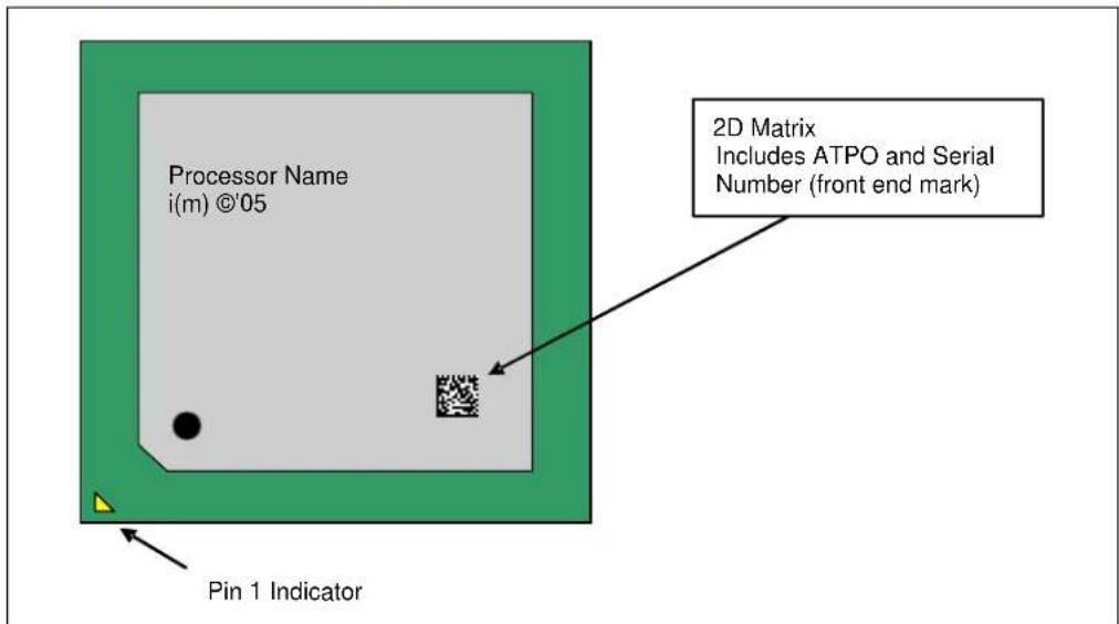
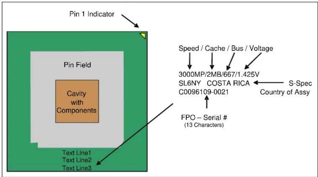
Figure 3-4 shows the topside markings and Figure 3-5 shows the bottom-side markings on the processor. These diagrams are to aid in the identification of the Dual-Core Intel Xeon processor 7000 series. Please note that the figures in this section are not to scale.
Figure 3-4. Processor Topside Markings
NOTES:
1. All characters will be in upper case.
Figure 3-5. Processor Bottom-Side Markings
3.9 Processor Pin-Out Coordinates
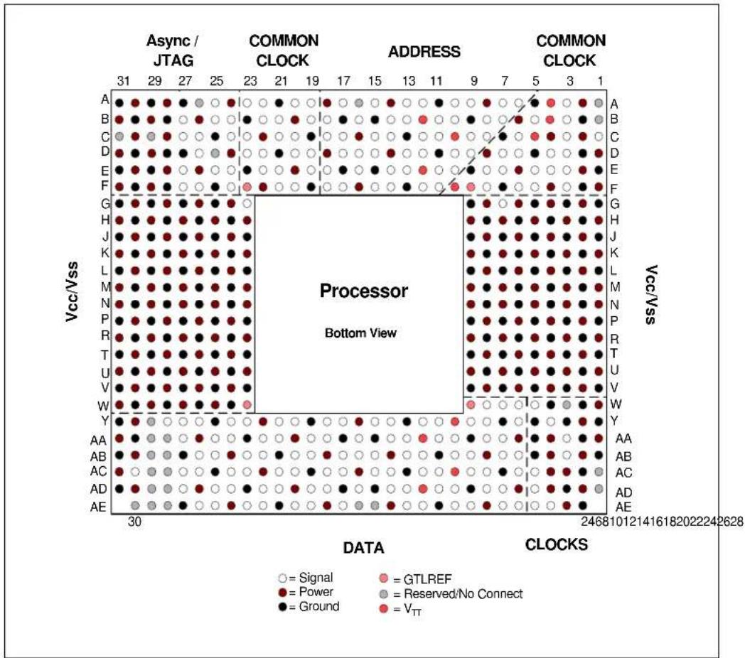
Figure 3-6 shows the top view of the processor pin coordinates. The coordinates are referred to throughout the document to identify processor pins.
Figure 3-6. Processor Pin-Out Coordinates, Top View
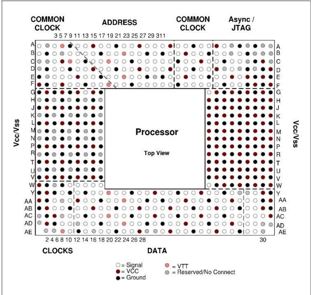
Figure 3-7. Processor Pin-Out Coordinates, Bottom View
4.1 Dual-Core Intel Xeon Processor 7000 Series Pin Assignments
Section 2.5 contains the front side bus signal groups for the Dual-Core Intel Xeon processor 7000 series (see Table 2-4). This section provides a sorted pin list in Table 4-1 and Table 4-2. Table 4-1 is a listing of all processor pins ordered alphabetically by pin name. Table 4-2 is a listing of all processor pins ordered by pin number.
4.1.1 Pin Listing by Pin Name
Table 4-1. Pin Listing by Pin Name
| Pin Name Pin | No. | Signal Buffer Type | Direction |
| A3# A22 Source | Sync Input/Output | ||
| A4# A20 Source | Sync Input/Output | ||
| A5# B18 Source | Sync Input/Output | ||
| A6# C18 Source | Sync Input/Output | ||
| A7# A19 Source | Sync Input/Output | ||
| A8# C17 Source | Sync Input/Output | ||
| A9# D17 Source | Sync Input/Output | ||
| A10# | A13 Source | Sync Input/Output | |
| A11# | B16 Source | Sync Input/Output | |
| A12# | B14 Source | Sync Input/Output | |
| A13# | B13 Source | Sync Input/Output | |
| A14# | A12 Source | Sync Input/Output | |
| A15# | C15 Source | Sync Input/Output | |
| A16# | C14 Source | Sync Input/Output | |
| A17# | D16 Source | Sync Input/Output | |
| A18# | D15 Source | Sync Input/Output | |
| A19# | F15 | Source Sync Input/Output | |
| A20# | A10 Source | Sync Input/Output | |
| A21# | B10 Source | Sync Input/Output | |
| A22# | B11 | Source Sync Input/Output | |
| A23# | C12 Source | Sync Input/Output | |
| A24# | E14 Source | Sync Input/Output | |
| A25# | D13 Source | Sync Input/Output | |
| A26# | A9 | Source Sync Input/Output | |
| A27# | B8 | Source Sync Input/Output | |
Table 4-1. Pin Listing by Pin Name (Cont'd)
| Pin Name Pin | No. | Signal Buffer Type | Direction |
| A28# | E13 Source Sync Input | Output | |
| A29# | D12 Source Sync Input | Output | |
| A30# | C11 Source Sync Input | Output | |
| A31# | B7 | Source Sync Input/Output | |
| A32# | A6 | Source Sync Input/Output | |
| A33# | A7 | Source Sync Input/Output | |
| A34# | C9 | Source Sync Input/Output | |
| A35# | C8 | Source Sync Source Sync | |
| A36# | F16 | Source Sync Source Sync | |
| A37# | F22 | Source Sync Source Sync | |
| A38# | B6 | Source Sync Source Sync | |
| A39# | C16 Source Sync Source Sync | ||
| A20M# | F27 | Async GTL+ | Input |
| ADS# | D19 Common Clk | Input/Output | |
| ADSTB0# | F17 | Source Sync | Input/Output |
| ADSTB1# | F14 | Source Sync | Input/Output |
| AP0# | E10 Common Clk | Input/Output | |
| AP1# | D9 | Common Clk | Input/Output |
| BCLK0 | Y4 | FSB Clk | Input |
| BCLK1 | W5 | FSB Clk | Input |
| BINIT# | F11 | Common Clk | Input/Output |
| BNR# | F20 | Common Clk | Input/Output |
| BOOT_SELECT | G7 | Power/Other | Input |
| BPM0# | F6 | Common Clk | Input/Output |
| BPM1# | F8 | Common Clk | Input/Output |
| BPM2# | E7 | Common Clk | Input/Output |
Table 4-1. Pin Listing by Pin Name (Cont'd)
| Pin Name | Pin No. | Signal Buffer Type | Direction |
| BPM3# F5 Common Clk Input/Output | |||
| BPM4# E8 Common Clk Input/Output | |||
| BPM5# E4 Common Clk Input/Output | |||
| BPRI# D23 Common Clk Input | |||
| BR0# D20 Common Clk Input/Output | |||
| BR1# F12 Common Clk Input/Output | |||
| BR2# E11 Common Clk Input/Output | |||
| BR3# D10 Common Clk Input/Output | |||
| BSEL0 AA3 Power/Other Output | |||
| BSEL1 AB3 Power/Other Output | |||
| COMP0 AD16 Power/Other Input | |||
| D0# | Y26 Source Sync Input/Output | ||
| D1# | AA27 Source Sync Input/Output | ||
| D2# | Y24 Source Sync Input/Output | ||
| D3# | AA25 Source Sync Input/Output | ||
| D4# | AD27 Source Sync Input/Output | ||
| D5# | Y23 Source Sync Input/Output | ||
| D6# | AA24 Source Sync Input/Output | ||
| D7# | AB26 Source Sync Input/Output | ||
| D8# | AB25 Source Sync Input/Output | ||
| D9# | AB23 Source Sync Input/Output | ||
| D10# | AA22 Source Sync Input/Output | ||
| D11# | AA21 Source Sync Input/Output | ||
| D12# | AB20 Source Sync Input/Output | ||
| D13# | AB22 Source Sync Input/Output | ||
| D14# | AB19 Source Sync Input/Output | ||
| D15# | AA19 Source Sync Input/Output | ||
| D16# | AE26 Source Sync Input/Output | ||
| D17# | AC26 Source Sync Input/Output | ||
| D18# | AD25 Source Sync Input/Output | ||
| D19# | AE25 Source Sync Input/Output | ||
| D20# | AC24 Source Sync Input/Output | ||
| D21# | AD24 Source Sync Input/Output | ||
| D22# | AE23 Source Sync Input/Output | ||
| D23# | AC23 Source Sync Input/Output | ||
| D24# | AA18 Source Sync Input/Output | ||
| D25# | AC20 Source Sync Input/Output | ||
| D26# | AC21 Source Sync Input/Output | ||
Table 4-1. Pin Listing by Pin Name (Cont'd)
| Pin Name | Pin No. | Signal Buffer Type | Direction |
| D27# | AE22 Source Sync Input/Output | ||
| D28# | AE20 Source Sync Input/Output | ||
| D29# | AD21 | Source Sync | Input/Output |
| D30# | AD19 | Source Sync | Input/Output |
| D31# | AB17 Source Sync Input/Output | ||
| D32# | AB16 Source Sync Input/Output | ||
| D33# | AA16 Source Sync Input/Output | ||
| D34# | AC17 | Source Sync | Input/Output |
| D35# | AE13 Source Sync Input/Output | ||
| D36# | AD18 | Source Sync | Input/Output |
| D37# | AB15 Source Sync Input/Output | ||
| D38# | AD13 | Source Sync | Input/Output |
| D39# | AD14 | Source Sync | Input/Output |
| D40# | AD11 | Source Sync | Input/Output |
| D41# | AC12 | Source Sync | Input/Output |
| D42# | AE10 Source Sync Input/Output | ||
| D43# | AC11 | Source Sync | Input/Output |
| D44# AE9 Source Sync Input/Output | |||
| D45# | AD10 | Source Sync | Input/Output |
| D46# AD8 Source Sync Input/Output | |||
| D47# AC9 Source Sync Input/Output | |||
| D48# | AA13 Source Sync Input/Output | ||
| D49# | AA14 Source Sync Input/Output | ||
| D50# | AC14 | Source Sync | Input/Output |
| D51# | AB12 Source Sync Input/Output | ||
| D52# | AB13 Source Sync Input/Output | ||
| D53# | AA11 | Source Sync | Input/Output |
| D54# | AA10 Source Sync Input/Output | ||
| D55# | AB10 Source Sync Input/Output | ||
| D56# AC8 Source Sync Input/Output | |||
| D57# AD7 Source Sync Input/Output | |||
| D58# AE7 Source Sync Input/Output | |||
| D59# AC6 Source Sync Input/Output | |||
| D60# AC5 Source Sync Input/Output | |||
| D61# AA8 Source Sync Input/Output | |||
| D62# | Y9 Source Sync Input/Output | ||
| D63# AB6 Source Sync Input/Output | |||
| DBI0# | AC27 Source Sync Input/Output | ||
Table 4-1. Pin Listing by Pin Name (Cont'd)
| Pin Name | Pin No. | Signal Buffer Type | Direction |
| DBI1# AD22 Source Sync Input/Output | |||
| DBI2# AE12 Source Sync Input/Output | |||
| DBI3# AB9 Source Sync Input/Output | |||
| DBSY# F18 Common Clk Input/Output | |||
| DEFER# C23 Common Clk Input | |||
| Don't Care A2 | |||
| Don't Care A26 | |||
| Don't Care A28 | |||
| Don't Care A30 | |||
| Don't Care A31 | |||
| Don't Care B4 | |||
| Don't Care B26 | |||
| Don't Care B29 | |||
| Don't Care B30 | |||
| Don't Care B31 | |||
| Don't Care C2 | |||
| Don't Care C28 | |||
| Don't Care C31 | |||
| Don't Care D1 | |||
| Don't Care D25 | |||
| Don't Care D27 | |||
| Don't Care D29 | |||
| Don't Care E2 | |||
| Don't Care H1 | |||
| Don't Care H3 | |||
| Don't Care H5 | |||
| Don't Care H7 | |||
| Don't Care H9 | |||
| Don't Care K1 | |||
| Don't Care K3 | |||
| Don't Care K5 | |||
| Don't Care K7 | |||
| Don't Care K9 | |||
| Don't Care M1 | |||
| Don't Care M3 | |||
| Don't Care M5 | |||
| Don't Care M7 | |||
| Don't Care M9 | |||
Table 4-1. Pin Listing by Pin Name (Cont'd)
| Pin Name | Pin No. | Signal Buffer Type | Direction |
| Don't Care N1 | |||
| Don't Care N3 | |||
| Don't Care N5 | |||
| Don't Care N7 | |||
| Don't Care N9 | |||
| Don't Care R1 | |||
| Don't Care R3 | |||
| Don't Care R5 | |||
| Don't Care R7 | |||
| Don't Care R9 | |||
| Don't Care U1 | |||
| Don't Care U3 | |||
| Don't Care U5 | |||
| Don't Care U7 | |||
| Don't Care U9 | |||
| Don't Care | AA4 | ||
| Don't Care | AC4 | ||
| Don't Care | AC30 | ||
| Don't Care | AD6 | ||
| Don't Care | AD30 | ||
| Don't Care | AD31 | ||
| Don't Care | AE2 | ||
| Don't Care | AE3 | ||
| Don't Care | AE8 | ||
| Don't Care | AE15 | ||
| Don't Care | AE16 | ||
| DP0# AC18 Common Clk Input/Output | |||
| DP1# AE19 Common Clk Input/Output | |||
| DP2# AC15 Common Clk Input/Output | |||
| DP3# AE17 Common Clk Input/Output | |||
| DRDY# | E18 Common Clk Input/Output | ||
| DSTBN0# Y21 Source Sync Input/Output | |||
| DSTBN1# Y18 Source Sync Input/Output | |||
| DSTBN2# Y15 Source Sync Input/Output | |||
| DSTBN3# Y12 Source Sync Input/Output | |||
| DSTBP0# | Y20 Source Sync Input/Output | ||
| DSTBP1# | Y17 Source Sync Input/Output | ||
| DSTBP2# | Y14 Source Sync Input/Output | ||
Table 4-1. Pin Listing by Pin Name (Cont'd)
| Pin Name | Pin No. | Signal Buffer Type | Direction |
| DSTBP3# Y11 Source Sync Input/Output | |||
| FERR#/PBE# E27 | Async GTL+ Output | ||
| FORCEPR# A15 | Async GTL+ Input | ||
| GTLREF0 W23 Power/Other | Input | ||
| GTLREF1 W9 Power/Other | Input | ||
| GTLREF2 F23 Power/Other | Input | ||
| GTLREF3 F9 Power/Other Input | |||
| HIT# | E22 Common Clk | Input/Output | |
| HITM# | A23 Common Clk | Input/Output | |
| IERR# | E5 Async GTL+ Output | ||
| IGNNE# | C26 Async GTL+ Input | ||
| INIT# | D6 | Async GTL+ Input | |
| LINT0/INTR | B24 Async GTL+ Input | ||
| LINT1/NMI | G23 | Async GTL+ Input | |
| LOCK# | A17 Common Clk | Input/Output | |
| MCERR# | D7 | Common Clk | Input/Output |
| ODTEN | B5 Power/Other Input | ||
| PROCHOT# | B25 Async GTL+ Output | ||
| PROCTYPE | Y31 Power/Other O | ||
| PWRGOOD AB7 | Async GTL+ Input | ||
| REQ0# | B19 Source Sync Input/Output | ||
| REQ1# | B21 Source Sync Input/Output | ||
| REQ2# | C21 | Source Sync Input/Output | |
| REQ3# | C20 | Source Sync Input/Output | |
| REQ4# | B22 Source Sync Input/Output | ||
| Reserved | C1 | ||
| Reserved | E16 | ||
| Reserved | W3 | ||
| Reserved | Y27 | ||
| Reserved | Y28 | ||
| Reserved AC1 | |||
| Reserved | AE30 | ||
| RESET# | Y8 Common Clk | Input | |
| RS0# | E21 Common Clk | Input | |
| RS1# | D22 | Common Clk | Input |
| RS2# | F21 | Common Clk | Input |
| RSP# | C6 | Common Clk | Input |
| SKTOCC# | A3 Power/Other Output | ||
Table 4-1. Pin Listing by Pin Name (Cont'd)
| Pin Name | Pin No. | Signal Buffer Type | Direction |
| SM_ALERT# | AD28 | SMBus | Output |
| SM_CLK | AC28 | SMBus | Input |
| SM_DAT | AC29 | SMBus | Input/Output |
| SM_EP_A0 | AA29 | SMBus | Input |
| SM_EP_A1 | AB29 | SMBus | Input |
| SM_EP_A2 | AB28 | SMBus | Input |
| SM_TS1_A0 | AA28 | SMBus | Input |
| SM_TS1_A1 | Y29 | SMBus | Input |
| SM_VCC | AE28 | Power/Other | |
| SM_VCC | AE29 | Power/Other | |
| SM_WP | AD29 | SMBus | Input |
| SMI# | C27 | Async GTL+ Input | |
| STPCLK# | D4 | Async GTL+ Input | |
| TCK | E24 TAP | Input | |
| TDI | C24 TAP | Input | |
| TDO | E25 TAP | Output | |
| TEST_BUS | A16 Power/Other Input | ||
| TESTHI0 | W6 Power/Other Input | ||
| TESTHI1 | W7 Power/Other Input | ||
| TESTHI2 | W8 Power/Other Input | ||
| TESTHI3 | Y6 Power/Other Input | ||
| TESTHI4 | AA7 | Power/Other Input | |
| TESTHI5 | AD5 | Power/Other Input | |
| TESTHI6 | AE5 | Power/Other Input | |
| THERMTRIP# | F26 Async GTL+ Output | ||
| TMS | A25 TAP | Input | |
| TRDY# | E19 Common Clk | Input | |
| TRST# | F24 TAP | Input | |
| V_CC | A8 Power/Other | ||
| V_CC | A14 Power/Other | ||
| V_CC | A18 Power/Other | ||
| V_CC | A24 Power/Other | ||
| V_CC | B20 Power/Other | ||
| V_CC | C4 | Power/Other | |
| V_CC | C22 Power/Other | ||
| V_CC | C30 Power/Other | ||
| V_CC | D8 | Power/Other | |
| V_CC | D14 Power/Other | ||
Table 4-1. Pin Listing by Pin Name (Cont'd)
| Pin Name Pin | No. | Signal Buffer Type | Direction |
| V_CC | D18 Power/Other | ||
| V_CC | D24 Power/Other | ||
| V_CC | D31 Power/Other | ||
| V_CC | E6 Power/Other | ||
| V_CC | E20 Power/Other | ||
| V_CC | E26 Power/Other | ||
| V_CC | E28 Power/Other | ||
| V_CC | E30 Power/Other | ||
| V_CC | F1 Power/Other | ||
| V_CC | F4 Power/Other | ||
| V_CC | F29 Power/Other | ||
| V_CC | F31 Power/Other | ||
| V_CC | G2 Power/Other | ||
| V_CC | G4 Power/Other | ||
| V_CC | G6 Power/Other | ||
| V_CC | G8 Power/Other | ||
| V_CC | G24 Power/Other | ||
| V_CC | G26 Power/Other | ||
| V_CC | G28 Power/Other | ||
| V_CC | G30 Power/Other | ||
| V_CC | H23 Power/Other | ||
| V_CC | H25 Power/Other | ||
| V_CC | H27 Power/Other | ||
| V_CC | H29 Power/Other | ||
| V_CC | H31 Power/Other | ||
| V_CC | J2 Power/Other | ||
| V_CC | J4 Power/Other | ||
| V_CC | J6 Power/Other | ||
| V_CC | J8 Power/Other | ||
| V_CC | J24 Power/Other | ||
| V_CC | J26 Power/Other | ||
| V_CC | J28 Power/Other | ||
| V_CC | J30 Power/Other | ||
| V_CC | K23 Power/Other | ||
| V_CC | K25 Power/Other | ||
| V_CC | K27 Power/Other | ||
| V_CC | K29 Power/Other | ||
| V_CC | K31 Power/Other |
Table 4-1. Pin Listing by Pin Name (Cont'd)
| Pin Name Pin | No. | Signal Buffer Type | Direction |
| V_CC | L2 Power/Other | ||
| V_CC | L4 Power/Other | ||
| V_CC | L6 Power/Other | ||
| V_CC | L8 Power/Other | ||
| V_CC | L24 Power/Other | ||
| V_CC | L26 Power/Other | ||
| V_CC | L28 Power/Other | ||
| V_CC | L30 Power/Other | ||
| V_CC | M23 Power/Other | ||
| V_CC | M25 Power/Other | ||
| V_CC | M27 Power/Other | ||
| V_CC | M29 Power/Other | ||
| V_CC | M31 Power/Other | ||
| V_CC | N23 Power/Other | ||
| V_CC | N25 Power/Other | ||
| V_CC | N27 Power/Other | ||
| V_CC | N29 Power/Other | ||
| V_CC | N31 Power/Other | ||
| V_CC | P2 Power/Other | ||
| V_CC | P4 Power/Other | ||
| V_CC | P6 Power/Other | ||
| V_CC | P8 Power/Other | ||
| V_CC | P24 Power/Other | ||
| V_CC | P26 Power/Other | ||
| V_CC | P28 Power/Other | ||
| V_CC | P30 Power/Other | ||
| V_CC | R23 Power/Other | ||
| V_CC | R25 Power/Other | ||
| V_CC | R27 Power/Other | ||
| V_CC | R29 Power/Other | ||
| V_CC | R31 Power/Other | ||
| V_CC | T2 Power/Other | ||
| V_CC | T4 Power/Other | ||
| V_CC | T6 Power/Other | ||
| V_CC | T8 Power/Other | ||
| V_CC | T24 Power/Other | ||
| V_CC | T26 Power/Other | ||
| V_CC | T28 Power/Other |
Table 4-1. Pin Listing by Pin Name (Cont'd)
| Pin Name Pin | No. | Signal Buffer Type | Direction |
| V_CC | T30 Power/Other | ||
| V_CC | U23 Power/Other | ||
| V_CC | U25 Power/Other | ||
| V_CC | U27 Power/Other | ||
| V_CC | U29 Power/Other | ||
| V_CC | U31 Power/Other | ||
| V_CC | V2 Power/Other | ||
| V_CC | V4 Power/Other | ||
| V_CC | V6 Power/Other | ||
| V_CC | V8 Power/Other | ||
| V_CC | V24 Power/Other | ||
| V_CC | V26 Power/Other | ||
| V_CC | V28 Power/Other | ||
| V_CC | V30 Power/Other | ||
| V_CC | W1 Power/Other | ||
| V_CC | W25 Power/Other | ||
| V_CC | W27 Power/Other | ||
| V_CC | W29 Power/Other | ||
| V_CC | W31 Power/Other | ||
| V_CC | Y2 Power/Other | ||
| V_CC | Y16 Power/Other | ||
| V_CC | Y22 Power/Other | ||
| V_CC | Y30 Power/Other | ||
| V_CC | AA1 Power/Other | ||
| V_CC | AA6 Power/Other | ||
| V_CC | AA20 Power/Other | ||
| V_CC | AA26 Power/Other | ||
| V_CC | AA31 Power/Other | ||
| V_CC | AB2 Power/Other | ||
| V_CC | AB8 Power/Other | ||
| V_CC | AB14 Power/Other | ||
| V_CC | AB18 Power/Other | ||
| V_CC | AB24 Power/Other | ||
| V_CC | AB30 Power/Other | ||
| V_CC | AC3 Power/Other | ||
| V_CC | AC16 Power/Other | ||
| V_CC | AC22 Power/Other | ||
| V_CC | AC31 Power/Other |
Table 4-1. Pin Listing by Pin Name (Cont'd)
| Pin Name Pin | No. | Signal Buffer Type | Direction |
| V_CC | AD2 Power/Other | ||
| V_CC | AD20 Power/Other | ||
| V_CC | AD26 Power/Other | ||
| V_CC | AE14 Power/Other | ||
| V_CC | AE18 Power/Other | ||
| V_CC | AE24 Power/Other | ||
| V_CCA | AB4 Power/Other Input | ||
| V_CCIOPLL | AD4 Power/Other Input | ||
| V_CCSENSE | B27 Power/Other Output | ||
| VID0 F3 Power/Other Output | |||
| VID1 E3 Power/Other Output | |||
| VID2 | D3 Power/Other Output | ||
| VID3 | C3 Power/Other Output | ||
| VID4 | B3 Power/Other Output | ||
| VID5 | A1 Power/Other Output | ||
| VIDPWRGD | B1 Power/Other Input | ||
| V_SS | A5 Power/Other | ||
| V_SS | A11 Power/Other | ||
| V_SS | A21 Power/Other | ||
| V_SS | A27 Power/Other | ||
| V_SS | A29 Power/Other | ||
| V_SS | B2 Power/Other | ||
| V_SS | B9 Power/Other | ||
| V_SS | B15 Power/Other | ||
| V_SS | B17 Power/Other | ||
| V_SS | B23 Power/Other | ||
| V_SS | B28 Power/Other | ||
| V_SS | C7 Power/Other | ||
| V_SS | C13 Power/Other | ||
| V_SS | C19 Power/Other | ||
| V_SS | C25 Power/Other | ||
| V_SS | C29 Power/Other | ||
| V_SS | D2 Power/Other | ||
| V_SS | D5 Power/Other | ||
| V_SS | D11 Power/Other | ||
| V_SS | D21 Power/Other | ||
| V_SS | D28 Power/Other | ||
| V_SS | D30 Power/Other | ||
Table 4-1. Pin Listing by Pin Name (Cont'd)
| Pin Name Pin | No. | Signal Buffer Type | Direction |
| V_SS | E9 Power/Other | ||
| V_SS | E15 Power/Other | ||
| V_SS | E17 Power/Other | ||
| V_SS | E23 Power/Other | ||
| V_SS | E29 Power/Other | ||
| V_SS | E31 Power/Other | ||
| V_SS | F2 Power/Other | ||
| V_SS | F7 Power/Other | ||
| V_SS | F13 Power/Other | ||
| V_SS | F19 Power/Other | ||
| V_SS | F25 Power/Other | ||
| V_SS | F28 Power/Other | ||
| V_SS | F30 Power/Other | ||
| V_SS | G1 Power/Other | ||
| V_SS | G3 Power/Other | ||
| V_SS | G5 Power/Other | ||
| V_SS | G9 Power/Other | ||
| V_SS | G25 Power/Other | ||
| V_SS | G27 Power/Other | ||
| V_SS | G29 Power/Other | ||
| V_SS | G31 Power/Other | ||
| V_SS | H2 Power/Other | ||
| V_SS | H4 Power/Other | ||
| V_SS | H6 Power/Other | ||
| V_SS | H8 Power/Other | ||
| V_SS | H24 Power/Other | ||
| V_SS | H26 Power/Other | ||
| V_SS | H28 Power/Other | ||
| V_SS | H30 Power/Other | ||
| V_SS | J1 Power/Other | ||
| V_SS | J3 Power/Other | ||
| V_SS | J5 Power/Other | ||
| V_SS | J7 Power/Other | ||
| V_SS | J9 Power/Other | ||
| V_SS | J23 Power/Other | ||
| V_SS | J25 Power/Other | ||
| V_SS | J27 Power/Other | ||
| V_SS | J29 Power/Other |
Table 4-1. Pin Listing by Pin Name (Cont'd)
| Pin Name Pin | No. | Signal Buffer Type | Direction |
| V_SS | J31 Power/Other | ||
| V_SS | K2 Power/Other | ||
| V_SS | K4 Power/Other | ||
| V_SS | K6 Power/Other | ||
| V_SS | K8 Power/Other | ||
| V_SS | K24 Power/Other | ||
| V_SS | K26 Power/Other | ||
| V_SS | K28 Power/Other | ||
| V_SS | K30 Power/Other | ||
| V_SS | L1 Power/Other | ||
| V_SS | L3 Power/Other | ||
| V_SS | L5 Power/Other | ||
| V_SS | L7 Power/Other | ||
| V_SS | L9 Power/Other | ||
| V_SS | L23 Power/Other | ||
| V_SS | L25 Power/Other | ||
| V_SS | L27 Power/Other | ||
| V_SS | L29 Power/Other | ||
| V_SS | L31 Power/Other | ||
| V_SS | M2 Power/Other | ||
| V_SS | M4 Power/Other | ||
| V_SS | M6 Power/Other | ||
| V_SS | M8 Power/Other | ||
| V_SS | M24 Power/Other | ||
| V_SS | M26 Power/Other | ||
| V_SS | M28 Power/Other | ||
| V_SS | M30 Power/Other | ||
| V_SS | N2 Power/Other | ||
| V_SS | N4 Power/Other | ||
| V_SS | N6 Power/Other | ||
| V_SS | N8 Power/Other | ||
| V_SS | N24 Power/Other | ||
| V_SS | N26 Power/Other | ||
| V_SS | N28 Power/Other | ||
| V_SS | N30 Power/Other | ||
| V_SS | P1 Power/Other | ||
| V_SS | P3 Power/Other | ||
| V_SS | P5 Power/Other | ||
Table 4-1. Pin Listing by Pin Name (Cont'd)
| Pin Name Pin | No. | Signal Buffer Type | Direction |
| V_SS | P7 Power/Other | ||
| V_SS | P9 Power/Other | ||
| V_SS | P23 Power/Other | ||
| V_SS | P25 Power/Other | ||
| V_SS | P27 Power/Other | ||
| V_SS | P29 Power/Other | ||
| V_SS | P31 Power/Other | ||
| V_SS | R2 Power/Other | ||
| V_SS | R4 Power/Other | ||
| V_SS | R6 Power/Other | ||
| V_SS | R8 Power/Other | ||
| V_SS | R24 Power/Other | ||
| V_SS | R26 Power/Other | ||
| V_SS | R28 Power/Other | ||
| V_SS | R30 Power/Other | ||
| V_SS | T1 Power/Other | ||
| V_SS | T3 Power/Other | ||
| V_SS | T5 Power/Other | ||
| V_SS | T7 Power/Other | ||
| V_SS | T9 Power/Other | ||
| V_SS | T23 Power/Other | ||
| V_SS | T25 Power/Other | ||
| V_SS | T27 Power/Other | ||
| V_SS | T29 Power/Other | ||
| V_SS | T31 Power/Other | ||
| V_SS | U2 Power/Other | ||
| V_SS | U4 Power/Other | ||
| V_SS | U6 Power/Other | ||
| V_SS | U8 Power/Other | ||
| V_SS | U24 Power/Other | ||
| V_SS | U26 Power/Other | ||
| V_SS | U28 Power/Other | ||
| V_SS | U30 Power/Other | ||
| V_SS | V1 Power/Other | ||
| V_SS | V3 Power/Other | ||
| V_SS | V5 Power/Other | ||
| V_SS | V7 Power/Other | ||
| V_SS | V9 Power/Other |
Table 4-1. Pin Listing by Pin Name (Cont'd)
| Pin Name Pin | No. | Signal Buffer Type | Direction |
| V_SS | V23 Power/Other | ||
| V_SS | V25 Power/Other | ||
| V_SS | V27 Power/Other | ||
| V_SS | V29 Power/Other | ||
| V_SS | V31 Power/Other | ||
| V_SS | W2 Power/Other | ||
| V_SS | W4 Power/Other | ||
| V_SS | W24 Power/Other | ||
| V_SS | W26 Power/Other | ||
| V_SS | W28 Power/Other | ||
| V_SS | W30 Power/Other | ||
| V_SS | Y1 Power/Other | ||
| V_SS | Y3 Power/Other | ||
| V_SS | Y5 Power/Other | ||
| V_SS | Y7 Power/Other | ||
| V_SS | Y13 Power/Other | ||
| V_SS | Y19 Power/Other | ||
| V_SS | Y25 Power/Other | ||
| V_SS | AA2 Power/Other | ||
| V_SS | AA9 Power/Other | ||
| V_SS | AA15 Power/Other | ||
| V_SS | AA17 Power/Other | ||
| V_SS | AA23 Power/Other | ||
| V_SS | AA30 Power/Other | ||
| V_SS | AB1 Power/Other | ||
| V_SS | AB5 Power/Other | ||
| V_SS | AB11 Power/Other | ||
| V_SS | AB21 Power/Other | ||
| V_SS | AB27 Power/Other | ||
| V_SS | AB31 Power/Other | ||
| V_SS | AC2 Power/Other | ||
| V_SS | AC7 Power/Other | ||
| V_SS | AC13 Power/Other | ||
| V_SS | AC19 Power/Other | ||
| V_SS | AC25 Power/Other | ||
| V_SS | AD3 Power/Other | ||
| V_SS | AD9 Power/Other | ||
| V_SS | AD15 Power/Other |
Table 4-1. Pin Listing by Pin Name (Cont'd)
| Pin Name Pin | No. | Signal Buffer Type | Direction |
| V_SS | AD17 Power/Other | ||
| V_SS | AD23 Power/Other | ||
| Vss AE6 Power/Other | |||
| V_SS | AE11 Power/Other | ||
| V_SS | AE21 Power/Other | ||
| V_SS | AE27 Power/Other | ||
| V_SSA | AA5 Power/Other Input | ||
| V_SSSENSE | D26 Power/Other Output | ||
| V_TT | A4 Power/Other | ||
| V_TT | B12 Power/Other |
Table 4-1. Pin Listing by Pin Name (Cont'd)
| Pin Name Pin | No. | Signal Buffer Type | Direction |
| V_TT | C5 Power/Other | ||
| V_TT | C10 Power/Other | ||
| V_TT | E12 Power/Other | ||
| V_TT | F10 Power/Other | ||
| V_TT | Y10 Power/Other | ||
| V_TT | AA12 Power/Other | ||
| V_TT | AC10 Power/Other | ||
| V_TT | AD12 Power/Other | ||
| V_TT | AE4 Power/Other | ||
| VTTEN E1 Power | Other Output |
4.1.2 Pin Listing by Pin Number
Table 4-2. Pin Listing by Pin Number
| Pin No. | Pin Name | Signal Buffer Type | Direction |
| A1 VID5 Power/Other Output | |||
| A2 Don't Care | |||
| A3 SKTOCC# Power/Other Output | |||
| A4 VTT | Power/Other | ||
| A5 VSS | Power/Other | ||
| A6 A32# Source Sync Input/Output | |||
| A7 A33# Source Sync Input/Output | |||
| A8 VCC | Power/Other | ||
| A9 A26# Source Sync Input/Output | |||
| A10 A20# Source Sync Input/Output | |||
| A11 V SS | Power/Other | ||
| A12 A14# Source Sync Input/Output | |||
| A13 A10# Source Sync Input/Output | |||
| A14 V CC | Power/Other | ||
| A15 FORCEPR# Async GTL+ Input | |||
| A16 TEST_BUS Power/Other Input | |||
| A17 LOCK# Common Clk Input/Output | |||
| A18 V cc | Power/Other | ||
| A19 A7# Source Sync Input/Output | |||
| A20 A4# Source Sync Input/Output | |||
| A21 V ss | Power/Other | ||
| A22 A3# Source Sync Input/Output | |||
| A23 HITM# Common Clk Input/Output | |||
| A24 V cc | Power/Other | ||
| A25 TMS TAP Input | |||
| A26 Don't Care | |||
| A27 V ss | Power/Other | ||
| A28 Don't Care | |||
| A29 V ss | Power/Other | ||
| A30 Don't Care | |||
| A31 Don't Care | |||
| B1 VIDPWRGD Power/Other Input | |||
| B2 VSS | Power/Other | ||
| B3 VID4 Power/Other Output | |||
| B4 Don't Care | |||
| B5 ODTEN Power/Other Input | |||
| B6 A38# Source Sync Input/Output | |||
| B7 A31# Source Sync Input/Output | |||
| B8 A27# Source Sync Input/Output | |||
Table 4-2. Pin Listing by Pin Number (Cont'd)
| Pin No. | Pin Name | Signal Buffer Type | Direction |
| B9 | V_SS | Power/Other | |
| B10 A2 | 1# Source Sync Input/Output | ||
| B11 A2 | 2# Source Sync Input/Output | ||
| B12 V | TT | Power/Other | |
| B13 A1 | 3# Source Sync Input/Output | ||
| B14 A1 | 2# Source Sync Input/Output | ||
| B15 V | ss | Power/Other | |
| B16 A1 | 1# Source Sync Input/Output | ||
| B17 V | ss | Power/Other | |
| B18 A5# | Source Sync Input/Output | ||
| B19 REQ0# | Common Clk Input/Output | ||
| B20 V | cc | Power/Other | |
| B21 REQ1# | Common Clk Input/Output | ||
| B22 REQ4# | Common Clk Input/Output | ||
| B23 V | ss | Power/Other | |
| B24 LINT0/INTR | Async GTL+ Input | ||
| B25 PROCHOT# | Async GTL+ Output | ||
| B26 Don't Care | |||
| B27 V | CCSENSE | Power/Other Output | |
| B28 V | ss | Power/Other | |
| B29 Don't Care | |||
| B30 Don't Care | |||
| B31 Don't Care | |||
| C1 Reserved | |||
| C2 Don't Care | |||
| C3 VID3 Power/Other Output | |||
| C4 | V_CC | Power/Other | |
| C5 | V_TT | Power/Other | |
| C6 RSP# | Common Clk | Input | |
| C7 | V_SS | Power/Other | |
| C8 A35 | # Source Sync Input/Output | ||
| C9 A34 | # Source Sync Input/Output | ||
| C10 V | TT | Power/Other | |
| C11 A30 | # Source Sync Input/Output | ||
| C12 A23 | # Source Sync Input/Output | ||
| C13 V | ss | Power/Other | |
| C14 A16 | # Source Sync Input/Output | ||
| C15 A15 | # Source Sync Input/Output | ||
| C16 A39 | # Source Sync Input/Output | ||
Table 4-2. Pin Listing by Pin Number (Cont'd)
| Pin No. | Pin Name | Signal Buffer Type | Direction |
| C17 A8 | # Source Sync Input/ | Output | |
| C18 A6 | # Source Sync Input/ | Output | |
| C19 V | ss | Power/Other | |
| C20 RE | Q3# Common Clk Input/ | Output | |
| C21 RE | Q2# Common Clk Input/ | Output | |
| C22 V | cc | Power/Other | |
| C23 DEFER | # Common Clk Input | ||
| C24 TDI | TAP Input | ||
| C25 V | ss | Power/Other Input | |
| C26 IGNNE | # Async GTL+ Input | ||
| C27 SMI | # Async GTL+ Input | ||
| C28 Don't Care | |||
| C29 V | ss | Power/Other | |
| C30 V | cc | Power/Other | |
| C31 Don't Care | |||
| D1 Don't Care | |||
| D2 | VSS | Power/Other | |
| D3 VID | 2 Power/Other Output | ||
| D4 ST | PCLK# | Async GTL+ Input | |
| D5 | VSS | Power/Other | |
| D6 INIT | # | Async GTL+ Input | |
| D7 MC | ERR# | Common Clk Input/ | Output |
| D8 | VCC | Power/Other | |
| D9 AP | 1# | Common Clk Input/ | Output |
| D10 BR | 3# | Common Clk Input/ | Output |
| D11 V | ss | Power/Other | |
| D12 A2 | 9# Source Sync Input/ | Output | |
| D13 A2 | 5# Source Sync Input/ | Output | |
| D14 V | cc | Power/Other | |
| D15 A1 | 8# Source Sync Input/ | Output | |
| D16 A1 | 7# Source Sync Input/ | Output | |
| D17 A9 | # Source Sync Input/ | Output | |
| D18 V | cc | Power/Other | |
| D19 ADS# | Common Clk Input/ | Output | |
| D20 BR0 | # | Common Clk Input/ | Output |
| D21 V | ss | Power/Other | |
| D22 RS1 | # | Common Clk Input | |
| D23 BPRI# | Common Clk Input | ||
| D24 V | cc | Power/Other | |
| D25 Don't Care | |||
| D26 V | SSSENSE | Power/Other Output | |
Table 4-2. Pin Listing by Pin Number (Cont'd)
| Pin No. | Pin Name | Signal Buffer Type | Direction |
| D27 Don't Care | |||
| D28 V | ss | Power/Other | |
| D29 Don't Care | |||
| D30 V | ss | Power/Other | |
| D31 V | cc | Power/Other | |
| E1 VTTEN Power/Other Output | |||
| E2 Don't Care | |||
| E3 VID1 Power/Other Output | |||
| E4 BPM5# Common Clk Input/Output | |||
| E5 IERR# Async GTL+ Output | |||
| E6 | V_CC | Power/Other | |
| E7 BPM2# Common Clk Input/Output | |||
| E8 BPM4# Common Clk Input/Output | |||
| E9 | V_SS | Power/Other | |
| E10 AP0# Common Clk Input/Output | |||
| E11 | BR2# | Common Clk Input/Output | |
| E12 V | TT | Power/Other | |
| E13 A28# Source Sync Input/Output | |||
| E14 A24# Source Sync Input/Output | |||
| E15 V | ss | Power/Other | |
| E16 Reserved | |||
| E17 V | ss | Power/Other | |
| E18 DRDY# Common Clk Input/Output | |||
| E19 TRDY# Common Clk Input | |||
| E20 V | cc | Power/Other | |
| E21 RS0# Common Clk Input | |||
| E22 HIT# Common Clk Input/Output | |||
| E23 V | ss | Power/Other | |
| E24 TCK TAP Input | |||
| E25 TDO TAP Output | |||
| E26 V | cc | Power/Other | |
| E27 FERR#/PBE# Async GTL+ Output | |||
| E28 V | cc | Power/Other | |
| E29 V | ss | Power/Other | |
| E30 V | cc | Power/Other | |
| E31 V | ss | Power/Other | |
| F1 | V_CC | Power/Other | |
| F2 | V_SS | Power/Other | |
| F3 | VID0 Power/Other Output | ||
| F4 | V_CC | Power/Other | |
| F5 | BPM3# Common Clk Input/Output | ||
Table 4-2. Pin Listing by Pin Number (Cont'd)
| Pin No. | Pin Name | Signal Buffer Type | Direction |
| F6 BPM0# Common Clk Input/Output | |||
| F7 | V_SS | Power/Other | |
| F8 BPM1# Common Clk Input/Output | |||
| F9 GTLREF3 Power/Other Input | |||
| F10 V | TT | Power/Other | |
| F11 BINIT# Common Clk Input/Output | |||
| F12 BR1# Common Clk Input/Output | |||
| F13 V | ss | Power/Other | |
| F14 ADSTB1# Source Sync Input/Output | |||
| F15 A19# Source Sync Input/Output | |||
| F16 A36# Source Sync Input/Output | |||
| F17 ADSTB0# Source Sync Input/Output | |||
| F18 DBSY# Common Clk Input/Output | |||
| F19 V | ss | Power/Other | |
| F20 BNR# Common Clk Input/Output | |||
| F21 RS2# Common Clk Input | |||
| F22 A37# Source Sync Input/Output | |||
| F23 GTLREF2 Power/Other Input | |||
| F24 TRST# TAP Input | |||
| F25 V | ss | Power/Other | |
| F26 THERMTRIP#Async GTL+ Output | |||
| F27 A20M# Async GTL+ Input | |||
| F28 V | ss | Power/Other | |
| F29 V | cc | Power/Other | |
| F30 V | ss | Power/Other | |
| F31 V | cc | Power/Other | |
| G1 | V_SS | Power/Other | |
| G2 | V_CC | Power/Other | |
| G3 | V_SS | Power/Other | |
| G4 | V_CC | Power/Other | |
| G5 | V_SS | Power/Other | |
| G6 | V_CC | Power/Other | |
| G7 | BOOT_SELECT | Power/Other Input | |
| G8 | V_CC | Power/Other | |
| G9 | V_SS | Power/Other | |
| G23 | LINT1/NMI | Async GTL+ | Input |
| G24 | V_CC | Power/Other | |
| G25 | V_SS | Power/Other | |
| G26 | V_CC | Power/Other | |
| G27 | V_SS | Power/Other | |
| G28 | V_CC | Power/Other | |
Table 4-2. Pin Listing by Pin Number (Cont'd)
| Pin No. | Pin Name | Signal Buffer Type | Direction |
| G29 | V_SS | Power/Other | |
| G30 | V_CC | Power/Other | |
| G31 | V_SS | Power/Other | |
| H1 | Don't Care | ||
| H2 | V_SS | ||
| H3 | Don't Care | ||
| H4 | V_SS | ||
| H5 | Don't Care | ||
| H6 | V_SS | ||
| H7 | Don't Care | ||
| H8 | V_SS | ||
| H9 | Don't Care | ||
| H23 | V_CC | Power/Other | |
| H24 | V_SS | Power/Other | |
| H25 | V_CC | Power/Other | |
| H26 | V_SS | Power/Other | |
| H27 | V_CC | Power/Other | |
| H28 | V_SS | Power/Other | |
| H29 | V_CC | Power/Other | |
| H30 | V_SS | Power/Other | |
| H31 | V_CC | Power/Other | |
| J1 | V_SS | Power/Other | |
| J2 | V_CC | Power/Other | |
| J3 | V_SS | Power/Other | |
| J4 | V_CC | Power/Other | |
| J5 | V_SS | Power/Other | |
| J6 | V_CC | Power/Other | |
| J7 | V_SS | Power/Other | |
| J8 | V_CC | Power/Other | |
| J9 | V_SS | Power/Other | |
| J23 V | ss | Power/Other | |
| J24 V | cc | Power/Other | |
| J25 V | ss | Power/Other | |
| J26 V | cc | Power/Other | |
| J27 V | ss | Power/Other | |
| J28 V | cc | Power/Other | |
| J29 V | ss | Power/Other | |
| J30 V | cc | Power/Other | |
| J31 V | ss | Power/Other | |
| K1 Don't Care | |||
| K2 | V_SS | Power/Other | |
Table 4-2. Pin Listing by Pin Number (Cont'd)
| Pin No. | Pin Name | Signal Buffer Type | Direction |
| K3 | Don't Care | ||
| K4 | V_SS | Power/Other | |
| K5 | Don't Care | ||
| K6 | V_SS | Power/Other | |
| K7 | Don't Care | ||
| K8 | V_SS | Power/Other | |
| K9 | Don't Care | ||
| K23 V | CC | Power/Other | |
| K24 V | SS | Power/Other | |
| K25 V | CC | Power/Other | |
| K26 V | SS | Power/Other | |
| K27 V | CC | Power/Other | |
| K28 V | SS | Power/Other | |
| K29 V | CC | Power/Other | |
| K30 V | SS | Power/Other | |
| K31 V | CC | Power/Other | |
| L1 | V_SS | Power/Other | |
| L2 | V_CC | Power/Other | |
| L3 | V_SS | Power/Other | |
| L4 | V_CC | Power/Other | |
| L5 | V_SS | Power/Other | |
| L6 | V_CC | Power/Other | |
| L7 | V_SS | Power/Other | |
| L8 | V_CC | Power/Other | |
| L9 | V_SS | Power/Other | |
| L23 V | SS | Power/Other | |
| L24 V | CC | Power/Other | |
| L25 V | SS | Power/Other | |
| L26 V | CC | Power/Other | |
| L27 V | SS | Power/Other | |
| L28 V | CC | Power/Other | |
| L29 V | SS | Power/Other | |
| L30 V | CC | Power/Other | |
| L31 V | SS | Power/Other | |
| M1 | Don't Care | ||
| M2 | V_SS | Power/Other | |
| M3 | Don't Care | ||
| M4 | V_SS | Power/Other | |
| M5 | Don't Care | ||
| M6 | V_SS | Power/Other | |
| M7 | Don't Care |
Table 4-2. Pin Listing by Pin Number (Cont'd)
| Pin No. | Pin Name | Signal Buffer Type | Direction |
| M8 | V_SS | Power/Other | |
| M9 Don't Care | |||
| M23 V | cc | Power/Other | |
| M24 V | ss | Power/Other | |
| M25 V | cc | Power/Other | |
| M26 V | ss | Power/Other | |
| M27 V | cc | Power/Other | |
| M28 V | ss | Power/Other | |
| M29 V | cc | Power/Other | |
| M30 V | ss | Power/Other | |
| M31 V | cc | Power/Other | |
| N1 Don't Care | |||
| N2 | V_SS | Power/Other | |
| N3 Don't Care | |||
| N4 | V_SS | Power/Other | |
| N5 Don't Care | |||
| N6 | V_SS | Power/Other | |
| N7 Don't Care | |||
| N8 | V_SS | Power/Other | |
| N9 Don't Care | |||
| N23 V | cc | Power/Other | |
| N24 V | ss | Power/Other | |
| N25 V | cc | Power/Other | |
| N26 V | ss | Power/Other | |
| N27 V | cc | Power/Other | |
| N28 V | ss | Power/Other | |
| N29 V | cc | Power/Other | |
| N30 V | ss | Power/Other | |
| N31 V | cc | Power/Other | |
| P1 | V_SS | Power/Other | |
| P2 | V_CC | Power/Other | |
| P3 | V_SS | Power/Other | |
| P4 | V_CC | Power/Other | |
| P5 | V_SS | Power/Other | |
| P6 | V_CC | Power/Other | |
| P7 | V_SS | Power/Other | |
| P8 | V_CC | Power/Other | |
| P9 | V_SS | Power/Other | |
| P23 V | ss | Power/Other | |
| P24 V | cc | Power/Other | |
| P25 V | ss | Power/Other | |
Table 4-2. Pin Listing by Pin Number (Cont'd)
| Pin No. | Pin Name | Signal Buffer Type | Direction |
| P26 V | cc | Power/Other | |
| P27 V | ss | Power/Other | |
| P28 V | cc | Power/Other | |
| P29 V | ss | Power/Other | |
| P30 V | cc | Power/Other | |
| P31 V | ss | Power/Other | |
| R1 Don't Care | |||
| R2 | V_SS | Power/Other | |
| R3 Don't Care | |||
| R4 | V_SS | Power/Other | |
| R5 Don't Care | |||
| R6 | V_SS | Power/Other | |
| R7 Don't Care | |||
| R8 | V_SS | Power/Other | |
| R9 Don't Care | |||
| R23 V | cc | Power/Other | |
| R24 V | ss | Power/Other | |
| R25 V | cc | Power/Other | |
| R26 V | ss | Power/Other | |
| R27 V | cc | Power/Other | |
| R28 V | ss | Power/Other | |
| R29 V | cc | Power/Other | |
| R30 V | ss | Power/Other | |
| R31 V | cc | Power/Other | |
| T1 | V_SS | Power/Other | |
| T2 | V_CC | Power/Other | |
| T3 | V_SS | Power/Other | |
| T4 | V_CC | Power/Other | |
| T5 | V_SS | Power/Other | |
| T6 | V_CC | Power/Other | |
| T7 | V_SS | Power/Other | |
| T8 | V_CC | Power/Other | |
| T9 | V_SS | Power/Other | |
| T23 V | ss | Power/Other | |
| T24 V | cc | Power/Other | |
| T25 V | ss | Power/Other | |
| T26 V | cc | Power/Other | |
| T27 V | ss | Power/Other | |
| T28 V | cc | Power/Other | |
| T29 V | ss | Power/Other | |
| T30 V | cc | Power/Other | |
Table 4-2. Pin Listing by Pin Number (Cont'd)
| Pin No. | Pin Name | Signal Buffer Type | Direction |
| T31 V | ss | Power/Other | |
| U1 Don't Care | |||
| U2 | V_SS | Power/Other | |
| U3 Don't Care | |||
| U4 | V_SS | Power/Other | |
| U5 Don't Care | |||
| U6 | V_SS | Power/Other | |
| U7 Don't Care | |||
| U8 | V_SS | Power/Other | |
| U9 Don't Care | |||
| U23 V | cc | Power/Other | |
| U24 V | ss | Power/Other | |
| U25 V | cc | Power/Other | |
| U26 V | ss | Power/Other | |
| U27 V | cc | Power/Other | |
| U28 V | ss | Power/Other | |
| U29 V | cc | Power/Other | |
| U30 V | ss | Power/Other | |
| U31 V | cc | Power/Other | |
| V1 | V_SS | Power/Other | |
| V2 | V_CC | Power/Other | |
| V3 | V_SS | Power/Other | |
| V4 | V_CC | Power/Other | |
| V5 | V_SS | Power/Other | |
| V6 | V_CC | Power/Other | |
| V7 | V_SS | Power/Other | |
| V8 | V_CC | Power/Other | |
| V9 | V_SS | Power/Other | |
| V23 V | ss | Power/Other | |
| V24 V | cc | Power/Other | |
| V25 V | ss | Power/Other | |
| V26 V | cc | Power/Other | |
| V27 V | ss | Power/Other | |
| V28 V | cc | Power/Other | |
| V29 V | ss | Power/Other | |
| V30 V | cc | Power/Other | |
| V31 V | ss | Power/Other | |
| W1 | V_CC | Power/Other | |
| W2 | V_SS | Power/Other | |
| W3 Reserved | |||
| W4 | V_SS | Power/Other | |
Table 4-2. Pin Listing by Pin Number (Cont'd)
| Pin No. | Pin Name | Signal Buffer Type | Direction |
| W5 | BCLK1 FSB Clk Input | ||
| W6 | TESTHI0 Power/Other Input | ||
| W7 | TESTHI1 Power/Other Input | ||
| W8 | TESTHI2 Power/Other Input | ||
| W9 | GTLREF1 Power/Other Input | ||
| W23 | GTLREF0 Power/Other Input | ||
| W24 V | SS | Power/Other | |
| W25 V | CC | Power/Other | |
| W26 V | SS | Power/Other | |
| W27 V | CC | Power/Other | |
| W28 V | SS | Power/Other | |
| W29 V | CC | Power/Other | |
| W30 V | SS | Power/Other | |
| W31 V | CC | Power/Other | |
| Y1 | VSS | Power/Other | |
| Y2 | VCC | Power/Other | |
| Y3 | VSS | Power/Other | |
| Y4 | BCLK0 FSB Clk Input | ||
| Y5 | VSS | Power/Other | |
| Y6 | TESTHI3 Power/Other Input | ||
| Y7 | VSS | Power/Other | |
| Y8 | RESET# Common Clk Input | ||
| Y9 | D62# Source Sync Input/Output | ||
| Y10 V | TT | Power/Other | |
| Y11 | DSTBP3# Source Sync Input/Output | ||
| Y12 | DSTBN3# Source Sync Input/Output | ||
| Y13 V | SS | Power/Other | |
| Y14 | DSTBP2# Source Sync Input/Output | ||
| Y15 | DSTBN2# Source Sync Input/Output | ||
| Y16 V | CC | Power/Other | |
| Y17 | DSTBP1# Source Sync Input/Output | ||
| Y18 | DSTBN1# Source Sync Input/Output | ||
| Y19 V | SS | Power/Other | |
| Y20 | DSTBP0# Source Sync Input/Output | ||
| Y21 | DSTBN0# Source Sync Input/Output | ||
| Y22 V | CC | Power/Other | |
| Y23 D5# | Source Sync Input/Output | ||
| Y24 D2# | Source Sync Input/Output | ||
| Y25 V | SS | Power/Other | |
| Y26 D0# | Source Sync Input/Output | ||
| Y27 Reserved | |||
Table 4-2. Pin Listing by Pin Number (Cont'd)
| Pin No. | Pin Name | Signal Buffer Type | Direction |
| Y28 | Reserved | ||
| Y29 | SM_TS1_A1 | SMBus Input | |
| Y30 V | CC | Power/Other | |
| Y31 | PROCTYPE | Power/Other O | |
| AA1 | V_CC | Power/Other | |
| AA2 | V_SS | Power/Other | |
| AA3 | BSEL0 | Power/Other Output | |
| AA4 | Don't Care | ||
| AA5 | V_SSA | Power/Other Input | |
| AA6 | V_CC | Power/Other | |
| AA7 | TESTHI4 Power/Other Input | ||
| AA8 | D61# Source Sync Input/Output | ||
| AA9 | V_SS | Power/Other | |
| AA10 | D54# Source Sync Input/Output | ||
| AA11 | D53# Source Sync Input/Output | ||
| AA12 | V_TT | Power/Other | |
| AA13 | D48# Source Sync Input/Output | ||
| AA14 | D49# Source Sync Input/Output | ||
| AA15 | V_SS | Power/Other | |
| AA16 | D33# Source Sync Input/Output | ||
| AA17 | V_SS | Power/Other | |
| AA18 | D24# Source Sync Input/Output | ||
| AA19 | D15# Source Sync Input/Output | ||
| AA20 | V_CC | Power/Other | |
| AA21 | D11# | Source Sync Input/Output | |
| AA22 | D10# Source Sync Input/Output | ||
| AA23 | V_SS | Power/Other | |
| AA24 | D6# | Source Sync Input/Output | |
| AA25 | D3# | Source Sync Input/Output | |
| AA26 | V_CC | Power/Other | |
| AA27 | D1# | Source Sync Input/Output | |
| AA28 | SM_TS1_A0 | SMBus | Input |
| AA29 | SM_EP_A0 | SMBus | Input |
| AA30 | V_SS | Power/Other | |
| AA31 | V_CC | Power/Other | |
| AB1 | V_SS | Power/Other | |
| AB2 | V_CC | Power/Other | |
| AB3 | BSEL1 | Power/Other Output | |
| AB4 | V_CCA | Power/Other Input | |
| AB5 | V_SS | Power/Other | |
| AB6 | D63# Source Sync Input/Output | ||
Table 4-2. Pin Listing by Pin Number (Cont'd)
| Pin No. | Pin Name | Signal Buffer Type | Direction |
| AB7 PW | WRGOOD Async GTL+ Input | ||
| AB8 V | cc | Power/Other | |
| AB9 DB13# Source Sync Input/Output | |||
| AB10 D55# Source Sync Input/Output | |||
| AB11 V | ss | Power/Other | |
| AB12 D51# Source Sync Input/Output | |||
| AB13 D52# Source Sync Input/Output | |||
| AB14 V | cc | Power/Other | |
| AB15 D87# Source Sync Input/Output | |||
| AB16 D82# Source Sync Input/Output | |||
| AB17 D81# Source Sync Input/Output | |||
| AB18 V | cc | Power/Other | |
| AB19 D14# Source Sync Input/Output | |||
| AB20 D12# Source Sync Input/Output | |||
| AB21 V | ss | Power/Other | |
| AB22 D13# Source Sync Input/Output | |||
| AB23 D9# Source Sync Input/Output | |||
| AB24 V | cc | Power/Other | |
| AB25 D8# Source Sync Input/Output | |||
| AB26 D7# Source Sync Input/Output | |||
| AB27 V | ss | Power/Other | |
| AB28 SM_EP_A2 SMBus Input | |||
| AB29 SM_EP_A1 SMBus Input | |||
| AB30 V | cc | Power/Other | |
| AB31 V | ss | Power/Other | |
| AC1 Reserved | |||
| AC2 V | ss | Power/Other | |
| AC3 V | cc | Power/Other | |
| AC4 Don't Care | |||
| AC5 D60# Source Sync Input/Output | |||
| AC6 D59# Source Sync Input/Output | |||
| AC7 V | ss | Power/Other | |
| AC8 D56# Source Sync Input/Output | |||
| AC9 D47# Source Sync Input/Output | |||
| AC10 V | TT | Power/Other | |
| AC11 D43# Source Sync Input/Output | |||
| AC12 D41# Source Sync Input/Output | |||
| AC13 V | ss | Power/Other | |
| AC14 D50# Source Sync Input/Output | |||
| AC15 DP2# Common Clk Input/Output | |||
| AC16 V | cc | Power/Other | |
Table 4-2. Pin Listing by Pin Number (Cont'd)
| Pin No. | Pin Name | Signal Buffer Type | Direction |
| AC17 D34# | Source Sync Input/Output | ||
| AC18 DP0# | Common Clk Input/Output | ||
| AC19 Vss | Power/Other | ||
| AC20 D25# | Source Sync Input/Output | ||
| AC21 D26# | Source Sync Input/Output | ||
| AC22 Vcc | Power/Other | ||
| AC23 D23# | Source Sync Input/Output | ||
| AC24 D20# | Source Sync Input/Output | ||
| AC25 Vss | Power/Other | ||
| AC26 D17# | Source Sync Input/Output | ||
| AC27 DBI0# | Source Sync Input/Output | ||
| AC28 SM_CLK | SMBus Input | ||
| AC29 SM_DAT | SMBus Output | ||
| AC30 Don't Care | |||
| AC31 Vcc | Power/Other | ||
| AD1 Reserved | |||
| AD2 Vcc | Power/Other | ||
| AD3 Vss | Power/Other | ||
| AD4 VCCIOPLL | Power/Other | Input | |
| AD5 TESTHI5 | Power/Other Input | ||
| AD6 Don't Care | |||
| AD7 D57# | Source Sync Input/Output | ||
| AD8 D46# | Source Sync Input/Output | ||
| AD9 Vss | Power/Other | ||
| AD10 D45# | Source Sync Input/Output | ||
| AD11 D40# | Source Sync Input/Output | ||
| AD12 VTT | Power/Other | ||
| AD13 D38# | Source Sync Input/Output | ||
| AD14 D39# | Source Sync Input/Output | ||
| AD15 Vss | Power/Other | ||
| AD16 COMP0 | Power/Other Input | ||
| AD17 Vss | Power/Other | ||
| AD18 D36# | Source Sync Input/Output | ||
| AD19 D30# | Source Sync Input/Output | ||
| AD20 Vcc | Power/Other | ||
| AD21 D29# | Source Sync Input/Output | ||
| AD22 DBI1# | Source Sync Input/Output | ||
| AD23 Vss | Power/Other | ||
| AD24 D21# | Source Sync Input/Output | ||
| AD25 D18# | Source Sync Input/Output | ||
| AD26 Vcc | Power/Other |
Table 4-2. Pin Listing by Pin Number (Cont'd)
| Pin No. | Pin Name | Signal Buffer Type | Direction |
| AD27 D4 | # Source Sync Input/Output | ||
| AD28 SM | ALERT# SMBus Output | ||
| AD29 SM | WP SMBus Input | ||
| AD30 Don't Care | |||
| AD31 Don't Care | |||
| AE2 Don't Care | |||
| AE3 Don't Care | |||
| AE4 V | TT | Power/Other | |
| AE5 TESTHI6 Power/Other Input | |||
| AE6 V | ss | Power/Other Input | |
| AE7 D5 | 8# Source Sync Input/Output | ||
| AE8 Don't Care | |||
| AE9 D4 | 4# Source Sync Input/Output | ||
| AE10 D4 | 2# Source Sync Input/Output | ||
| AE11 V | ss | Power/Other | |
| AE12 DB | 2# Source Sync Input/Output | ||
| AE13 D3 | 5# Source Sync Input/Output | ||
Table 4-2. Pin Listing by Pin Number (Cont'd)
| Pin No. | Pin Name | Signal Buffer Type | Direction |
| AE14 V | cc | Power/Other | |
| AE15 D | don't Care | ||
| AE16 D | don't Care | ||
| AE17 DP3# | Common Clk Input/Output | ||
| AE18 V | cc | Power/Other | |
| AE19 DP1# | Common Clk Input/Output | ||
| AE20 DP28# Source Sync Input/Output | |||
| AE21 V | ss | Power/Other | |
| AE22 DP27# Source Sync Input/Output | |||
| AE23 DP22# Source Sync Input/Output | |||
| AE24 V | cc | Power/Other | |
| AE25 DP19# Source Sync Input/Output | |||
| AE26 DP16# Source Sync Input/Output | |||
| AE27 V | ss | Power/Other | |
| AE28 SM_VCC | Power/Other | ||
| AE29 SM_VCC | Power/Other | ||
| AE30 Reserved | |||
Pin Listing
intel®
5 Signal Definitions
5.1 Signal Definitions
Table 5-1. Signal Definitions (Sheet 1 of 7)
| Name Type | Description | ||
| A[39:3]# I/O A[39:3]# (Address) define a 240-byte physical memory address space. In sub-phase 1 of the address phase, these pins transmit the address of a transaction. In sub-phase 2, these pins transmit transaction type information. These signals must connect the appropriate pins of all agents on the Dual-Core Intel Xeon processor 7000 series FSB. A[39:3]# are protected by parity signals AP[1:0]#. A[39:3]# are source synchronous signals and are latched into the receiving buffers by ADSTB[1:0]#. On the active-to-inactive transition of RESET#, the processors sample a subset of the A[39:3]# pins to determine their power-on configuration. See Section 7.1. | |||
| A20M# | I | If A20M# (Address-20 Mask) is asserted, the processor masks physical address bit 20 (A20#) before looking up a line in any internal cache and before driving a read/write transaction on the bus. Asserting A20M# emulates the 8086 processor's address wrap-around at the 1-Mbyte boundary. Assertion of A20M# is only supported in real mode.A20M# is an asynchronous signal. However, to ensure recognition of this signal following an I/O write instruction, it must be valid 6 clks before the I/O write's response. | |
| ADS# I/O ADS# | (Address Strobe) is asserted to indicate the validity of the transaction address on the A[39:3]# and transaction request type on REQ[4:0]# pins. All bus agents observe the ADS# activation to begin parity checking, protocol checking, address decode, internal snoop, or deferred reply ID match operations associated with the new transaction. This signal must connect the appropriate pins on all Dual-Core Intel Xeon processor 7000 series FSB agents. | ||
| ADSTB[1:0]# I/O | Address strobes are used to latch A[39:3]# and REQ[4:0]# on their rising and falling edge. | ||
| AP[1:0]# | I/O | AP[1:0]# (Address Parity) are driven by the requestor one common clock after ADS#, A[39:3]#, REQ[4:0]# are driven. A correct parity signal is electrically high if an even number of covered signals are electrically low and electrically low if an odd number of covered signals are electrically low. This allows parity to be electrically high when all the covered signals are electrically high. AP[1:0]# should connect the appropriate pins of all Dual-Core Intel Xeon processor 7000 series FSB agents. The following table defines the coverage for these signals. | |
| Request Signals | Subphase 1 Subphase 2 | ||
| A[39:24]# | AP0# | ||
| A[23:3]# | AP1# | ||
| REQ[4:0]# | AP1# | ||
| BCLK[1:0] | I | The differential bus clock pair BCLK[1:0] determines the bus frequency. All processor FSB agents must receive these signals to drive their outputs and latch their inputs.All external timing parameters are specified with respect to the rising edge of BCLK0 crossing the falling edge of BCLK1. | |
| BINIT# I/O BINIT# (Bus Initialization) may be observed and driven by all processor FSB agents. If used, BINIT# must connect the appropriate pins of all such agents. If the BINIT# driver is enabled, BINIT# is asserted to signal any bus condition that prevents reliable future operation.If BINIT# observation is enabled during power-on configuration (see Section 7.1) and BINIT# is sampled asserted, symmetric agents reset their bus LOCK# activity and bus request arbitration state machines. The bus agents do not reset their I/O Queue (IOQ) and transaction tracking state machines upon observation of BINIT# assertion. Once the BINIT# assertion has been observed, the bus agents will re-arbitrate for the FSB and attempt completion of their bus queue and IOQ entries.If BINIT# observation is enabled during power on configuration, a central agent may handle an assertion of BINIT# as appropriate to the error handling architecture of the system. | |||
Table 5-1. Signal Definitions (Sheet 2 of 7)
| Name Type | Description | |||
| BNR# | I/O | BNR# (Block Next Request) is used to assert a bus stall by any bus agent who is unable to accept new bus transactions. During a bus stall, the current bus owner cannot issue any new transactions.Since multiple agents might need to request a bus stall at the same time, BNR# is a wire-OR signal which must connect the appropriate pins of all processor system bus agents. In order to avoid wire-OR glitches associated with simultaneous edge transitions driven by multiple drivers, BNR# is activated on specific clock edges and sampled on specific clock edges. | ||
| BOOT_SELECT | I The | BOOT_SELECT input informs the processor whether the platform supports the Dual-Core Intel Xeon processor 7000 series. Incompatible platform designs will have this input connected to VSS. Thus, this pin is essentially an electrical key to prevent the Dual-Core Intel Xeon processor 7000 series from running in a system that is not designed for it. For platforms that are designed to support the Dual-Core Intel Xeon processor 7000 series, this pin should be changed to a no-connect. | ||
| BPM[5:0]# | I/O | BPM[5:0]# (Breakpoint Monitor) are breakpoint and performance monitor signals. They are outputs from the processor which indicate the status of breakpoints and programmable counters used for monitoring processor performance. BPM[5:0]# should connect the appropriate pins of all Dual-Core Intel Xeon processor 7000 series FSB agents.BPM4# provides PRDY# (Probe Ready) functionality for the TAP port. PRDY# is a processor output used by debug tools to determine processor debug readiness.BPM5# provides PREQ# (Probe Request) functionality for the TAP port. PREQ# is used by debug tools to request debug operation of the processors.BPM[5:4]# must be bussed to all bus agents. Please refer to the appropriate platform design guide for more detailed information. | ||
| BPRI# I BPRI# (Bus Priority Request) is used to arbitrate for ownership of the processor FSB. It must connect the appropriate pins of all processor FSB agents. Observing BPRI# active (as asserted by the priority agent) causes all other agents to stop issuing new requests, unless such requests are part of an ongoing locked operation. The priority agent keeps BPRI# asserted until its requests are issued, then releases the bus by deasserting BPRI#. | ||||
| BR[3:0]# | I/O | BR[3:0]# (Bus Request) drive the BREQ[3:0]# signals in the system. The BREQ[3:0]# signals are interconnected in a rotating manner to individual processor pins. The tables below give the rotating interconnect between the processor and bus signals for 3-load configurations.BR[3:0]# Signals Rotating Interconnect, 3-Load Configuration | ||
| Bus Signal | Agent 0 Pins | Agent 1 Pins | ||
| BREQ0# | BR0# | BR1# | ||
| BREQ1# | BR1# | BR0# | ||
| BREQ2# | BR2# | BR3# | ||
| BREQ3# | BR3# | BR2# | ||
| During power-on configuration, the central agent must assert the BREQ0# bus signal. All symmetric agents sample their BR[3:0]# pins on the active-to-inactive transition of RESET#. The pin which the agent samples asserted determines its agent ID. | ||||
| BSEL[1:0] | O | These output signals are used to select the FSB frequency. The frequency is determined by the processor(s), chipset, and frequency synthesizer capabilities. All FSB agents must operate at the same frequency. Individual processors will only operate at their specified FSB frequency. See the appropriate platform design guide for implementation examples.See Table 2-2 for output values. Refer to the appropriate platform design guide for termination recommendations. | ||
| COMP0 I COMP0 must be terminated to V SS on the baseboard using precision resistors. This input configures the AGTL+ drivers of the processor. Refer to the appropriate platform design guide for implementation details. | ||||
Table 5-1. Signal Definitions (Sheet 3 of 7)
| Name Type | Description | ||
| D[63:0]# | I/O | D[63:0]# (Data) are the data signals. These signals provide a 64-bit data path between the processor FSB agents, and must connect the appropriate pins on all such agents. The data driver asserts DRDY# to indicate a valid data transfer.D[63:0]# are quad-pumped signals, and will thus be driven four times in a common clock period.D[63:0]# are latched off the falling edge of both DSTBP[3:0]# and DSTBN[3:0]#. Each group of 16 data signals correspond to a pair of one DSTBP# and one DSTBN#. The following table shows the grouping of data signals to strobes and DBI#.Furthermore, the DBI# pins determine the polarity of the data signals. Each group of 16 data signals corresponds to one DBI# signal. When the DBI# signal is active, the corresponding data group is inverted and therefore sampled active high. | |
| DBI[3:0]# | I/O | DBI[3:0]# are source synchronous and indicate the polarity of the D[63:0]# signals. The DBI[3:0]# signals are activated when the data on the data bus is inverted. If more than half the data bits, within a 16-bit group, would have been asserted electronically low, the bus agent may invert the data bus signals for that particular sub-phase for that 16-bit group.DBI[3:0] Assignment To Data Bus | |
| Bus Signal Data | Bus Signals | ||
| DBI0# | D[15:0]# | ||
| DBI1# | D[31:16]# | ||
| DBI2# | D[47:32]# | ||
| DBI3# | D[63:48]# | ||
| DBSY# | I/O | DBSY# (Data Bus Busy) is asserted by the agent responsible for driving data on the processor FSB to indicate that the data bus is in use. The data bus is released after DBSY# is deasserted. This signal must connect the appropriate pins on all processor FSB agents. | |
| DEFER# I DEFER# is asserted by an agent to indicate that a transaction cannot be guaranteed in-order completion. Assertion of DEFER# is normally the responsibility of the addressed memory or I/O agent. This signal must connect the appropriate pins of all processor FSB agents. | |||
| DP[3:0]# | I/O | DP[3:0]# (Data Parity) provide optional parity protection for the data bus. They are driven by the agent responsible for driving D[63:0]#, and, if parity is implemented, must connect the appropriate pins of all bus agents which use them. | |
| DRDY# | I/O | DRDY# (Data Ready) is asserted by the data driver on each data transfer, indicating valid data on the data bus. In a multi-common clock data transfer, DRDY# may be deasserted to insert idle clocks. This signal must connect the appropriate pins of all processor FSB agents. | |
| DSTBN[3:0]# I/O | Data strobe used to latch in D[63:0]# and DBI[3:0]#. | ||
| DSTBP[3:0]# I/O | Data strobe used to latch in D[63:0]# and DBI[3:0]#. | ||
| FERR#/PBE# | O | FERR#/PBE# (floating-point error/pending break event) is a multiplexed signal and its meaning is qualified by STPCLK#. When STPCLK# is not asserted, FERR#/PBE# indicates a floating-point error and will be asserted when the processor detects an unmasked floating-point error. When STPCLK# is not asserted, FERR#/PBE# is similar to the ERROR# signal on the Intel® 387 coprocessor, and is included for compatibility with systems using MS-DOS*-type floating-point error reporting. When STPCLK# is asserted, an assertion of FERR#/PBE# indicates that the processor has a pending break event waiting for service. The assertion of FERR#/PBE# indicates that the processor should be returned to the Normal state. For additional information on the pending break event functionality, including the identification of support of the feature and enable/disable information, refer to Vol 3 of the IA-32 Intel® Architecture Software Developer's Manual and the AP-485 Intel® Processor Identification and the CPUID Instruction application note. | |
| FORCEPR# I This input can be used to force activation of the Thermal Control Circuit. | |||
| GTLREF[3:0] | I | GTLREF determines the signal reference level for AGTL+ input pins. GTLREF is used by the AGTL+ receivers to determine if a signal is an electrical 0 or an electrical 1. | |
Table 5-1. Signal Definitions (Sheet 4 of 7)
| Name Type | Description | |
| HIT# | I/O | HIT# (Snoop Hit) and HITM# (Hit Modified) convey transaction snoop operation results. Any FSB agent may assert both HIT# and HITM# together to indicate that it requires a snoop stall, which can be continued by reasserting HIT# and HITM# together, every other common clock.Since multiple agents may deliver snoop results at the same time, HIT# and HITM# are wire-OR signals which must connect the appropriate pins of all processor FSB agents. In order to avoid wire-OR glitches associated with simultaneous edge transitions driven by multiple drivers, HIT# and HITM# are activated on specific clock edges and sampled on specific clock edges. |
| HITM# | I/O | |
| IERR# | O | IERR# (Internal Error) is asserted by a processor as the result of an internal error. Assertion of IERR# is usually accompanied by a SHUTDOWN transaction on the processor FSB. This transaction may optionally be converted to an external error signal (e.g., NMI) by system core logic. The processor will keep IERR# asserted until the assertion of RESET#. |
| IGNNE# | I | IGNNE# (Ignore Numeric Error) is asserted to force the processor to ignore a numeric error and continue to execute noncontrol floating-point instructions. If IGNNE# is deasserted, the processor generates an exception on a noncontrol floating-point instruction if a previous floating-point instruction caused an error. IGNNE# has no effect when the NE bit in control register 0 (CR0) is set. IGNNE# is an asynchronous signal. However, to ensure recognition of this signal following an I/O write instruction, it must be valid a 6 clks before the I/O write's response. |
| INIT# | I | INIT# (Initialization), when asserted, resets integer registers inside all processors without affecting their internal caches or floating-point registers. Each processor then begins execution at the power-on Reset vector configured during power-on configuration. The processor continues to handle snoop requests during INIT# assertion. INIT# is an asynchronous signal and must connect the appropriate pins of all processor FSB agents.If INIT# is sampled active on the active to inactive transition of RESET#, then the processor executes its Built-in Self-Test (BIST). |
| LINT0/INTR LINT1/NMI | I LINT[1:0] (Local APIC Interrupt) must connect the appropriate pins of all FSB agents. When the APIC functionality is disabled, the LINT0 signal becomes INTR, a maskable interrupt request signal, and LINT1 becomes NMI, a nonmaskable interrupt. INTR and NMI are backward compatible with the signals of those names on the Pentium processor. Both signals are asynchronous.These signals must be software configured via BIOS programming of the APIC register space to be used either as NMI/INTR or LINT[1:0]. Because the APIC is enabled by default after Reset, operation of these pins as LINT[1:0] is the default configuration. | |
| LOCK# | I/O | LOCK# indicates to the system that a set of transactions must occur atomically. This signal must connect the appropriate pins of all processor FSB agents. For a locked sequence of transactions, LOCK# is asserted from the beginning of the first transaction to the end of the last transaction.When the priority agent asserts BPRI# to arbitrate for ownership of the processor FSB, it will wait until it observes LOCK# deasserted. This enables symmetric agents to retain ownership of the processor FSB throughout the bus locked operation and ensure the atomicity of lock. |
| MCERR# | I/O | MCERR# (Machine Check Error) is asserted to indicate an unrecoverable error or a bus protocol violation. It may be driven by all processor FSB agents.MCERR# assertion conditions are configurable at a system level. Assertion options are defined as follows:Enabled or disabled.Asserted, if configured, for internal errors along with IERR#.Asserted, if configured, by the request initiator of a bus transaction after it observes an error.Asserted by any bus agent when it observes an error in a bus transaction.For more details regarding machine check architecture, refer to the IA-32 Intel® Software Developer's Manual, Volume 3: System Programming Guide or the BIOS Writer's Guide which includes the Dual-Core Intel Xeon processor 7000 series.Since multiple agents may drive this signal at the same time, MCERR# is a wired-OR signal which must connect the appropriate pins of all processor FSB agents. In order to avoid wire-OR glitches associated with simultaneous edge transitions driven by multiple drivers, MCERR# is activated on specific clock edges and sampled on specific clock edges. |
Table 5-1. Signal Definitions (Sheet 5 of 7)
| Name | Type | Description |
| ODTEN I ODTEN | (On-die termination enable) should be connected to V through a resistor to enable on-die termination for end bus agents. For middle bus agents, pull this signal down via a resistor to ground to disable on-die termination. Whenever ODTEN is high, on-die termination will be active, regardless of other states of the bus. | |
| PROCHOT# | O | The assertion of PROCHOT# (processor hot) indicates that the processor die temperature has reached its thermal limit. See Section 6.2.3 for more details. |
| PROCTYPE | O | PROCTYPE is used to identify when the Dual-Core Intel Xeon processor 7000 series is installed. This pin should be used to toggle logic needed for the Dual-Core Intel Xeon processor 7000 series/64-bit Intel® Xeon® Processor MP with up to 8MB L3 Cache or 64-bit Intel® Xeon® Processor MP with 1MB L2 Cache. The pin is left floating on the Dual-Core Intel® Xeon® Processor 7000 Series package while on the 64-bit Intel® Xeon® Processor MP with up to 8MB L3 Cache packages this pin connects to V_SS |
| PWRGOOD | I | PWRGOOD (Power Good) is an input. The processor requires this signal to be a clean indication that all Dual-Core Intel Xeon processor 7000 series clocks and power supplies are stable and within their specifications. “Clean” implies that the signal will remain low (capable of sinking leakage current), without glitches, from the time that the power supplies are turned on until they come within specification. The signal must then transition monotonically to a high state.The PWRGOOD signal must be supplied to the processor. This signal is used to protect internal circuits against voltage sequencing issues. It should be driven high throughout boundary scan operation. |
| REQ[4:0]# | I/O | REQ[4:0]# (Request Command) must connect the appropriate pins of all processor FSB agents. They are asserted by the current bus owner to define the currently active transaction type. These signals are source synchronous to ADSTB[1:0]#. Refer to the AP[1:0]# signal description for details on parity checking of these signals. |
| RESET# | I | Asserting the RESET# signal resets all processors to known states and invalidates their internal caches without writing back any of their contents. For a power-on Reset, RESET# must stay active for at least 1 ms after Vcc and BCLK have reached their specified levels. On observing active RESET#, all FSB agents will deassert their outputs within two clocks. RESET# must not be kept asserted for more than 10 ms after PWRGOOD is asserted.A number of bus signals are sampled at the active-to-inactive transition of RESET# for power-on configuration. These configuration options are described in Section 7.1. |
| RS[2:0]# | I | RS[2:0]# (Response Status) are driven by the response agent (the agent responsible for completion of the current transaction), and must connect the appropriate pins of all processor FSB agents. |
| RSP# | I | RSP# (Response Parity) is driven by the response agent (the agent responsible for completion of the current transaction) during assertion of RS[2:0]#, the signals for which RSP# provides parity protection. It must connect to the appropriate pins of all processor FSB agents.A correct parity signal is electrically high if an even number of covered signals are electrically low and electrically low if an odd number of covered signals are electrically low. If RS[2:0]# are all electrically high, RSP# is also electrically high, since this indicates it is not being driven by any agent guaranteeing correct parity. |
| SKTOCC# | O | SKTOCC# (Socket occupied) will be pulled to ground by the processor to indicate that the processor is present. There is no connection to the processor silicon for this signal. |
| SM_ALERT# | O | SM_ALERT# (SMBus Alert) is an asynchronous interrupt line associated with the SMBus Thermal Sensor device. It is an open-drain output and the processor includes a 10 kΩ pull-up resistor to SM_VCC for this signal. For more information on the usage of the SM_ALERT# pin, see Section 7.4.7. |
| SM_CLK | I/O | The SM_CLK (SMBus Clock) signal is an input clock to the system management logic which is required for operation of the system management features of the Dual-Core Intel Xeon processor 7000 series. This clock is driven by the SMBus controller and is asynchronous to other clocks in the processor. The processor includes a 10 kΩ pull-up resistor to SM_VCC for this signal. |
| SM_DAT | I/O | The SM_DAT (SMBus Data) signal is the data signal for the SMBus. This signal provides the single-bit mechanism for transferring data between SMBus devices. The processor includes a 10 kΩ pull-up resistor to SM_VCC for this signal. |
Table 5-1. Signal Definitions (Sheet 6 of 7)
| Name | Type | Description |
| SM_EP_A[2:0] | I | The SM_EP_A (EEPROM Select Address) pins are decoded on the SMBus in conjunction with the upper address bits in order to maintain unique addresses on the SMBus in a system with multiple processors. To set an SM_EP_A line high, a pull-up resistor should be used that is no larger than 1 kΩ The processor includes a 10 kΩ pull-down resistor to V_SS for each of these signals.For more information on the usage of these pins, see Section 7.4.8. |
| SM_TS_A[1:0] | I | The SM_TS_A (Thermal Sensor Select Address) pins are decoded on the SMBus in conjunction with the upper address bits in order to maintain unique addresses on the SMBus in a system with multiple processors.The device's addressing, as implemented, includes a Hi-Z state for both address pins. The use of the Hi-Z state is achieved by leaving the input floating (unconnected).For more information on the usage of these pins, see Section 7.4.8. |
| SM_VCC | I | SM_VCC provides power to the SMBus components on the Dual-Core Intel Xeon processor 7000 series package. |
| SM_WP | I | WP (Write Protect) can be used to write protect the Scratch EEPROM. The Scratch EEPROM is write-protected when this input is pulled high to SM_VCC. The processor includes a 10 kΩ pull-down resistor to V_SS for this signal. |
| SMI# | I | SMI# (System Management Interrupt) is asserted asynchronously by system logic. On accepting a System Management Interrupt, processors save the current state and enter System Management Mode (SMM). An SMI Acknowledge transaction is issued, and the processor begins program execution from the SMM handler.If SMI# is asserted during the deassertion of RESET#, the processor will tri-state its outputs. |
| STPCLK# | I | STPCLK# (Stop Clock), when asserted, causes processors to enter a low power Stop-Grant state. The processor issues a Stop-Grant Acknowledge transaction, and stops providing internal clock signals to all processor core units except the FSB and APIC units. The processor continues to snoop bus transactions and service interrupts while in Stop-Grant state. When STPCLK# is deasserted, the processor restarts its internal clock to all units and resumes execution. The assertion of STPCLK# has no effect on the bus clock; STPCLK# is an asynchronous input. |
| TCK I TCK (Test Clock) | Clock) provides the clock input for the processor Test Access Port. | |
| TDI | I | TDI (Test Data In) transfers serial test data into the processor. TDI provides the serial input needed for JTAG specification support. |
| TDO O TDO (Test Data Out) | I | transfers serial test data out of the processor. TDO provides the serial output needed for JTAG specification support. |
| TEST_BUS | I | Must be connected to all other processor TEST_BUS signals in the system. See the appropriate platform design guideline for termination details. |
| TESTHI[6:0] | I | TESTHI[6:0] must be connected to a V TT power source through a resistor for proper processor operation. See Section 2.3 for more details. |
| THERMTRIP# | O | The processor protects itself from catastrophic overheating by use of an internal thermal sensor. To ensure that there are no false trips, THERMTRIP# (Thermal Trip) will activate at a temperature that is about 20°C above the maximum case temperature ( T_C ). Once activated, the processor will stop all execution and the signal remains latched until RESET# goes active. There is no hysteresis built into the thermal sensor itself; as long as the die temperature drops below the trip level, a RESET# pulse will reset the processor and execution will continue. If the temperature has not dropped below the trip level, the processor will continue to drive THERMTRIP# and remain stopped. |
| TMS | I | TMS (Test Mode Select) is a JTAG specification support signal used by debug tools. |
| TRDY# | I | TRDY# (Target Ready) is asserted by the target (chipset) to indicate that it is ready to receive a write or implicit writeback data transfer. TRDY# must connect the appropriate pins of all FSB agents. |
| TRST# | I | TRST# (Test Reset) resets the Test Access Port (TAP) logic. TRST# must be driven electrically low during power on Reset. Please refer to the eXtended Debug Port: Debug Port Design Guide for Twin Castle Chipset Platforms or the eXtended Debug Port: Debug Port Design Guide for MP Platforms for details. |
| V_CC | I | V_CC provides power to the core logic of the Dual-Core Intel Xeon processor 7000 series. |
Table 5-1. Signal Definitions (Sheet 7 of 7)
| Name Type | Description | |
| V_CCA | I | V_CCA provides isolated power for the analog portion of the internal PLL's. Use a discrete RLC filter to provide clean power. Refer to the appropriate platform design guide for complete implementation details. |
| V_CCIOPLL | I | V_CCIOPLL provides isolated power for digital portion of the internal PLL's. Follow the guidelines for V_CCA , and refer to the appropriate platform design guide for complete implementation details. |
| V_CCSENSE V_SSSENSE | O | V_CCSENSE and V_SSSENSE provide isolated, low impedance connections to the processor core voltage ( V_CC ) and ground ( V_SS ). They can be used to sense or measure voltage or ground near the silicon with little noise. |
| VID[5:0] | O | VID[5:0] (Voltage ID) pins are used to support automatic selection of power supply voltages ( V_CC ). These are open drain signals that are driven by the processor and must be pulled through a resistor. Conversely, the VR output must be disabled prior to the voltage supply for these pins becoming invalid. The VID pins are needed to support processor voltage specification variations. SeeTable 2-3for definitions of these pins. The V_CC VR must supply the voltage that is requested by these pins, or disable itself. |
| VIDPWRGD | I | The processor requires this input to determine that the supply voltage for BSEL[1:0] and VID[5:0] is stable and within specification. |
| V_SS | I | V_SS is the ground plane for the Dual-Core Intel Xeon processor 7000 series. |
| V_SSA | I | V_SSA provides an isolated,internalground for internal PLL's. Do not connect directly to ground. This pin is to be connected to V_CCA and V_CCIOPLL through a discrete filter circuit. |
| V_TT | I | V_TT is the FSB termination voltage. |
| VTTEN O VTTEN | can be used as an output enable for the V TTregulator. VTTEN is used as an electrical key to prevent processors with mechanically-equivalent pinouts from accidentally booting in a Dual-Core Intel Xeon processor 7000 series platform. Since VTTEN is an open circuit on the processor package, VTTEN must be pulled up on the motherboard. Refer to the appropriate platform design guide for implementation details. | |
6 Thermal Specifications
6.1 Package Thermal Specifications
The Dual-Core Intel Xeon processor 7000 series requires a thermal solution to maintain temperatures within operating limits. Any attempt to operate the processor outside these operating limits may result in permanent damage to the processor and potentially other components within the system. As processor technology changes, thermal management becomes increasingly crucial when building computer systems. Maintaining the proper thermal environment is key to reliable, long-term system operation.
A complete solution includes both component and system level thermal management features. Component level thermal solutions can include active or passive heatsinks attached to the processor IHS. Typical system level thermal solutions may consist of system fans combined with ducting and venting.
For more information on designing a component level thermal solution, refer to the Dual-Core Intel® Xeon® Processor 7000 Sequence Thermal/Mechanical Design Guidelines.
Note: The boxed processor will ship with a component thermal solution. Refer to Section 8 for details on the boxed processor.
6.1.1 Thermal Specifications
To allow the optimal operation and long-term reliability of Intel processor-based systems, the processor must remain within the minimum and maximum case temperature ( T_CASE ) specifications as defined by the applicable thermal profile (see Table 6-1 and Figure 6-1). Thermal solutions not designed to provide this level of thermal capability may affect the long-term reliability of the processor and system. For more details on thermal solution design, please refer to the appropriate processor thermal/mechanical design guideline.
The Dual-Core Intel Xeon processor 7000 series introduces a new methodology for managing processor temperatures which is intended to support acoustic noise reduction through fan speed control and assure processor reliability. Selection of the appropriate fan speed will be based on the temperature reported by the processor's Thermal Diode. If the diode temperature is greater than or equal to Tcontrol (see Section 6.2.6), then the processor case temperature must remain at or below the temperature as specified by the thermal profile (see Figure 6-1). If the diode temperature is less than Tcontrol, then the case temperature is permitted to exceed the thermal profile, but the diode temperature must remain at or below Tcontrol. Systems that implement fan speed control must be designed to take these conditions into account. Systems that do not alter the fan speed only need to guarantee the case temperature meets the thermal profile specifications.
The Dual-Core Intel Xeon processor 7000 series thermal profile ensures adherence to Intel reliability requirements. The thermal profile is representative of a volumetrically unconstrained thermal solution (i.e. industry enabled 2U heatsink). In this scenario, it is expected that the Thermal Control Circuit (TCC) would only be activated for very brief periods of time when running the most power intensive applications. Refer to the Dual-Core Intel® Xeon® Processor 7000 Sequence Thermal/Mechanical Design Guidelines for details on system thermal solution design, thermal profiles, and environmental considerations.
The upper point of the thermal profile consists of the Thermal Design Power (TDP) defined in Table 6-1 and the associated T_CASE value. The lower point of the thermal profile consists of x = P_CONTROL_BASE and y = T_CASE_MAX @ P_CONTROL_BASE. Pcontrol is defined as the processor power at which T_CASE, calculated from the thermal profile, corresponds to the lowest possible value of Tcontrol. This point is associated with the Tcontrol value (see Section 6.2.6) However, because Tcontrol represents a diode temperature, it is necessary to define the associated case temperature. This is T_CASE_MAX @ P_CONTROL_BASE. Please see Section 6.2.6 and the Dual-Core Intel® Xeon® Processor 7000 Sequence Thermal/Mechanical Design Guidelines for proper usage of the Tcontrol specification.
The case temperature is defined at the geometric top center of the processor IHS. Analysis indicates that real applications are unlikely to cause the processor to consume maximum power dissipation for sustained time periods. Intel recommends that complete thermal solution designs target the TDP indicated in Table 6-1, instead of the maximum processor power consumption. The Thermal Monitor feature is intended to help protect the processor in the event that an application exceeds the TDP recommendation for a sustained time period. For more details on this feature, refer to Section 6.2. To ensure maximum flexibility for future requirements, systems should be designed to the FMB guidelines, even if a processor with a lower thermal dissipation is currently planned. Thermal Monitor must be enabled for the processor to remain within specification.
Table 6-1. Dual-Core Intel® Xeon® Processor 7000 Series Thermal Specifications
| Core Frequency (GHz) | Maximum Power (W) | Thermal Design Power (W) | Minimum T_CASE (°C) | Maximum T_CASE (°C) | Notes |
| 2.66 GHz - FMB | 173 | 165 | 5 | See Figure 6-1; Table 6-2 | 1, 2, 3, 4 |
NOTES:
- These values are specified at V_CC_MAX for all processor frequencies. Systems must be designed to ensure the processor is not to be subjected to any static V_CC and I_CC combination wherein V_CC exceeds V_CC_MAX at specified I_CC . Please refer to the V_CC static and transient tolerance specifications in Section 2.
- Maximum Power is the maximum thermal power that can be dissipated by the processor through the integrated heat spreader (IHS). Maximum Power is measured at maximum T_CASE
- Thermal Design Power (TDP) should be used for processor/chipset thermal solution design targets. TDP is not the maximum power that the processor can dissipate. TDP is measured at maximum T_CASE .
- These specifications are based on final silicon characterization.
Figure 6-1. Dual-Core Intel® Xeon® Processor 7000 Series Thermal Profile A
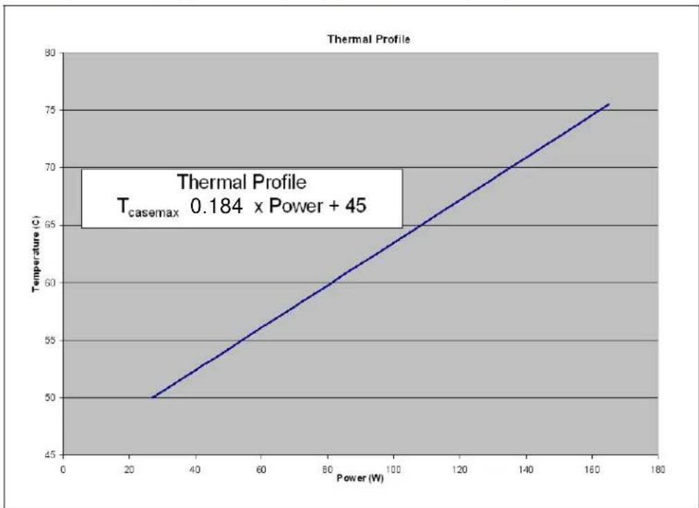
line
| Power (W) | Temperature (°C) | | --------- | ---------------- | | 25 | 50 | | 165 | 75 |NOTE: Refer to the Dual-Core Intel ^ Xeon ^ Processor 7000 Sequence Thermal/Mechanical Design Guidelines for system and environmental implementation details.
Table 6-2. Dual-Core Intel® Xeon® Processor 7000 Series Thermal Profile A
| Thermal Profile A | |
| _ca = 0.184 C /W; T | _A = 45 ^ |
| Power Temperature (°C) | |
| 27 50 | |
| 30 51 | |
| 40 52 | |
| 50 54 | |
| 60 56 | |
| 70 58 | |
| 80 60 | |
| 90 62 | |
| 100 64 | |
| 110 65 | |
| 120 67 | |
| 130 69 | |
| 140 71 | |
| 150 73 | |
| 160 75 | |
| 165 76 | |
6.1.2 Thermal Metrology
The maximum and minimum case temperatures ( T_CASE ) specified in Table 6-1 are measured at the geometric top center of the processor IHS. Figure 6-2 illustrates the location where T_CASE temperature measurements should be made. For detailed guidelines on temperature measurement methodology, refer to the Dual-Core Intel ^ Xeon ^ Processor 7000 Sequence Thermal/Mechanical Design Guidelines.
Figure 6-2. Case Temperature ( T_CASE ) Measurement Location
![Measure from edge of IHS 15.5 mm [0.610 In] 15.5 mm [0.610 In] Measure T_CASE at this point (geometric center of IHS) 53.34 mm FC-mPGA4 Package Thermal grease should cover entire area of IHS](/content/2026/05/1140870/images/370c8ac976b6c13c47e6ce2224cefe39f4e395650ac4f0b4d97dad649508d2f1.jpg)
6.2 Processor Thermal Features
6.2.1 Thermal Monitor
The Thermal Monitor feature helps control the processor temperature by activating the TCC when the processor silicon reaches its maximum operating temperature. The TCC reduces processor power consumption as needed by modulating (starting and stopping) the internal processor core clocks. The Thermal Monitor must be enabled for the processor to be operating within specifications. The temperature at which Thermal Monitor activates the thermal control circuit is not user configurable and is not software visible. Bus traffic is snooped in the normal manner, and interrupt requests are latched (and serviced during the time that the clocks are on) while the TCC is active.
When the Thermal Monitor is enabled and a high temperature situation exists (i.e. TCC is active), the clocks will be modulated by alternately turning the clocks off and on at a duty cycle specific to the processor (typically 30-50%). Clocks will not be off for more than 3 microseconds when the TCC is active. Cycle times are processor speed dependent and will decrease as processor core frequencies increase. A small amount of hysteresis has been included to prevent rapid active/inactive transitions of the TCC when the processor temperature is near its maximum
operating temperature. Once the temperature has dropped below the maximum operating temperature and the hysteresis timer has expired, the TCC goes inactive and clock modulation ceases.
With a thermal solution designed to meet the thermal profile, it is anticipated that the TCC would only be activated for very short periods of time when running the most power intensive applications. The processor performance impact due to these brief periods of TCC activation is expected to be so minor that it would be immeasurable. A thermal solution that is significantly under-designed may not be capable of cooling the processor even when the TCC is active continuously. Refer to the Dual-Core Intel ^® Xeon ^® Processor 7000 Sequence Thermal/Mechanical Design Guidelines for information on designing a thermal solution.
The duty cycle for the TCC, when activated by the Thermal Monitor, is factory configured and cannot be modified. The Thermal Monitor does not require any additional hardware, software drivers, or interrupt handling routines.
6.2.2 On-Demand Mode
The processor provides an auxiliary mechanism that allows system software to force the processor to reduce its power consumption. This mechanism is referred to as “On-Demand” mode and is distinct from the Thermal Monitor feature. On-Demand mode is intended as a means to reduce system level power consumption. Systems utilizing the Dual-Core Intel Xeon processor 7000 series must not rely on software usage of this mechanism to limit the processor temperature.
If bit 4 of the IA32_CLOCK_MODULATION MSR is written to a '1', the processor will immediately reduce its power consumption via modulation (starting and stopping) of the internal core clock, independent of the processor temperature. When using On-Demand mode, the duty cycle of the clock modulation is programmable via bits 3:1 of the IA32_CLOCK_MODULATION MSR. In On-Demand mode, the duty cycle can be programmed from 12.5% on/87.5% off to 87.5% on/12.5% off in 12.5% increments. On-Demand mode may be used in conjunction with the Thermal Monitor. If the system tries to enable On-Demand mode at the same time the TCC is engaged, the factory configured duty cycle of the TCC will override the duty cycle selected by the On-Demand mode.
6.2.3 PROCHOT# Signal Pin
An external signal, PROCHOT# (processor hot), is asserted when the processor die temperature has reached its factory configured trip point. If the Thermal Monitor is enabled (note that the Thermal Monitor must be enabled for the processor to be operating within specification), the TCC will be active when PROCHOT# is asserted. The processor can be configured to generate an interrupt upon the assertion or deassertion of PROCHOT#. Refer to the IA-32 Intel® Architecture Software Developer's Manual and the Prescott, Nocona and Potomac Processor BIOS Writer's Guide (BWG) for specific register and programming details.
PROCHOT# is designed to assert at or a few degrees higher than maximum T_CASE (as specified by the thermal profile) when dissipating TDP power, and cannot be interpreted as an indication of processor case temperature. This temperature delta accounts for processor package, lifetime, and manufacturing variations and attempts to ensure the Thermal Control Circuit is not activated below maximum T_CASE when dissipating TDP power. There is no defined or fixed correlation between the PROCHOT# trip temperature, the case temperature, or the thermal diode temperature. Thermal solutions must be designed to the processor specifications and cannot be adjusted based on experimental measurements of T_CASE , PROCHOT#, or Tdiode on random processor samples.
6.2.4 FORCEPR# Signal Pin
The FORCEPR# (force power reduction) input can be used by the platform to force the Dual-Core Intel Xeon processor 7000 series processor to activate the TCC. If the Thermal Monitor is enabled, the TCC will be activated upon the assertion of the FORCEPR# signal. The TCC will remain active until the system deasserts FORCEPR#. FORCEPR# is an asynchronous input. FORCEPR# can be used to thermally protect other system components. To use the voltage regulator (VR) as an example, when the FORCEPR# pin is asserted, the TCC in the processor will activate, reducing the current consumption of the processor and the corresponding temperature of the VR.
It should be noted that assertion of FORCEPR# does not automatically assert PROCHOT#. As mentioned previously, the PROCHOT# signal is asserted when a high temperature situation is detected. A minimum pulse width of 500 microseconds is recommended when FORCEPR# is asserted by the system. Sustained activation of the FORCEPR# pin may cause noticeable platform performance degradation.
Refer to the appropriate platform design guide for details on implementing the FORCEPR# signal feature.
6.2.5 THERMTRIP# Signal Pin
Regardless of whether or not Thermal Monitor is enabled, in the event of a catastrophic cooling failure, the processor will automatically shut down when the silicon has reached an elevated temperature (refer to the THERMTRIP# definition in Table 5-1). At this point, the system bus signal THERMTRIP# will go active and stay active as described in Table 5-1. THERMTRIP# activation is independent of processor activity and does not generate any bus cycles. Intel also recommends removal of V_TT .
6.2.6 Tcontrol and Fan Speed Reduction
Tcontrol is a temperature specification based on a temperature reading from the thermal diode. The value for Tcontrol will be calibrated in manufacturing and configured for each processor. The Tcontrol temperature for a given processor can be obtained by reading the IA32_TEMPERATURE_TARGET MSR in the processor. The Tcontrol value that is read from the IA32_TEMPERATURE_TARGET MSR must be converted from Hexadecimal to Decimal and added to a base value of 50 °C.
The value of Tcontrol may vary from 0x00h to 0x1Eh. Refer to the Prescott, Nocona and Potomac Processor BIOS Writer's Guide (BWG) for specific register details.
When Tdiode is above Tcontrol, then T_CASE must be at or below T_CASE_MAX as defined by the thermal profile (see Figure 6-1 and Table 6-2). Otherwise, the processor temperature can be maintained at Tcontrol.
6.2.7 Thermal Diode
The processor incorporates an thermal diode on each processor core. A thermal sensor located on the processor package monitors the die temperature of each core for thermal management/long term die temperature change purposes. The thermal diode is separate from the Thermal Monitor's thermal sensor and cannot be used to predict the behavior of the Thermal Monitor.
7.1 Power-On Configuration Options
Several configuration options can be set by hardware. The Dual-Core Intel Xeon processor 7000 series samples its hardware configuration at reset, on the active-to-inactive transition of RESET#. For specifications on these options, refer to Table 7-1.
The sampled information configures the processor for subsequent operation. These configuration options can only be changed by another reset. All resets configure the processor. For most reset purposes, the processor does not distinguish between a “warm” reset and a “power-on” reset.
Table 7-1. Power-On Configuration Option Pins
| Configuration Option Pin Notes | ||
| Output tri state SMI# | 1, 2 | |
| Execute BIST (Built-In Self Test) INIT# | 1, 2 | |
| In Order Queue de-pipelining (set IOQ depth to 1) | A7# | 1, 2 |
| Disable MCERR# observation | A9# | 1, 2 |
| Disable BINIT# observation | A10# | 1, 2 |
| Disable bus parking | A15# | 1, 2 |
| APIC Cluster ID | A[12:11]# | 1, 2 |
| Symmetric agent arbitration ID BR[3:0]# | 1, 2 | |
| Disable Hyper-Threading Technology | A31# | 1, 2,3 |
NOTES:
-
Asserting this signal during RESET# will select the corresponding option.
-
Address pins not identified in this table as configuration options should not be asserted during RESET#.
-
This mode is not tested.
7.2 Clock Control and Low Power States
The processor allows the use of HALT and Stop-Grant states to reduce power consumption by stopping the clock to internal sections of the processor, depending on each particular state. The Dual-Core Intel Xeon processor 7000 series also adds support for the Enhanced HALT state. For more configuration details also refer to the Prescott, Nocona and Potomac Processor BIOS Writer's Guide. See Figure 7-1 for a visual representation of the processor low power states.
7.2.1 Normal State
This is the normal operating state for the processor.
7.2.2 HALT Power Down State
HALT is a low power state entered when the processor executes the HALT instruction. The processor transitions to the Normal state upon the occurrence of SMI#, BINIT#, INIT#, LINT[1:0] (NMI, INTR), or an interrupt delivered over the FSB. RESET# causes the processor to immediately initialize itself.
The return from a System Management Interrupt (SMI) handler can be to either Normal Mode or the HALT Power Down state. See the IA-32 Intel® Architecture Software Developer's Manual, Volume III: System Programmer's Guide for more information.
The system can generate a STPCLK# while the processor is in the HALT Power Down state. When the system deasserts the STPCLK# interrupt, the processor returns execution to the HALT state.
While in HALT Power Down state, the processor processes bus snoops and interrupts.
Figure 7-1. Stop Clock State Machine
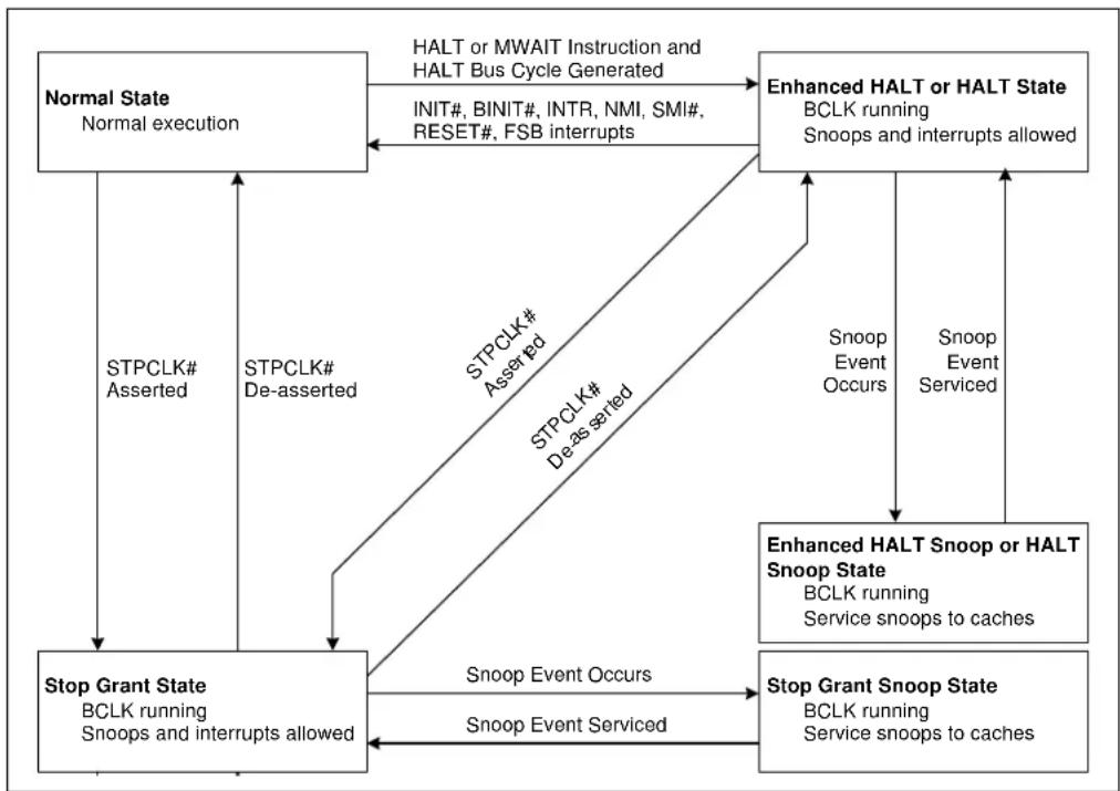
flowchart
graph TD
    A["Normal State\nNormal execution"] -->|STPCLK# Asserted| B["Stop Grant State\nBCLK running\nSnoops and interrupts allowed"]
    A -->|STPCLK# De-asserted| B
    B -->|STPCLK# Asserted STPCLK# De-as serted| C["Enhanced HALT or HALT State\nBCLK running\nSnoops and interrupts allowed"]
    C -->|Snoop Event Occurs| D["Enhanced HALT Snoop or HALT Snoop State\nBCLK running\nService snoops to caches"]
    C -->|Snoop Event Serviced| E["Stop Grant Snoop State\nBCLK running\nService snoops to caches"]
    A <-->|HALT or MWAIT Instruction and HALT Bus Cycle Generated\nINIT#, BINIT#, INTR, NMI, SMI#, RESET#, FSB interrupts| C
7.2.3 Stop-Grant State
When the STPCLK# pin is asserted, the Stop-Grant state of the processor is entered 20 bus clocks after the response phase of the processor-issued Stop Grant Acknowledge special bus cycle. For the Dual-Core Intel Xeon processor 7000 series, both logical processors must be in the Stop-Grant state before the deassertion of STPCLK#.
Since the AGTL+ signal pins receive power from the FSB, these pins should not be driven (allowing the level to return to V_TT ) for minimum power drawn by the termination resistors in this state. In addition, all other input pins on the FSB should be driven to the inactive state.
BINIT# is not serviced while the processor is in Stop-Grant state. The event is latched and can be serviced by software upon exit from the Stop-Grant state.
RESET# causes the processor to immediately initialize itself, but the processor will stay in Stop-Grant state. A transition back to the Normal state occurs with the deassertion of the STPCLK# signal.
A transition to the HALT/Grant Snoop state occurs when the processor detects a snoop on the FSB (see Section 7.2.4).
While in the Stop-Grant state, SMI#, INIT#, BINIT# and LINT[1:0] are latched by the processor, and only serviced when the processor returns to the Normal state. Only one occurrence of each event is recognized upon return to the Normal state.
While in Stop-Grant state, the processor processes snoops on the FSB and latches interrupts delivered on the FSB.
The PBE# signal can be driven when the processor is in Stop-Grant state. PBE# is asserted if there is any pending interrupt latched within the processor. Pending interrupts that are blocked by the EFLAGS.IF bit being clear still cause assertion of PBE#. Assertion of PBE# indicates to system logic that it should return the processor to the Normal state.
7.2.4 HALT/Grant Snoop State
The processor responds to snoop or interrupt transactions on the FSB while in Stop-Grant state or in HALT Power Down state. During a snoop or interrupt transaction, the processor enters the HALT/Grant Snoop state. The processor stays in this state until the snoop on the FSB has been serviced (whether by the processor or another agent on the FSB) or the interrupt has been latched. After the snoop is serviced or the interrupt is latched, the processor will return to the Stop-Grant state or HALT Power Down state, as appropriate.
7.2.5 Enhanced HALT Powerdown State
Enhanced HALT state is a low power state entered when all logical processors have executed the HALT or MWAIT instruction and Enhanced HALT state has been enabled via the BIOS. When one of the logical processors executes the HALT instruction, that logical processor is halted; however, the other processor continues normal operation. The Enhanced HALT state is generally a lower power state than the Stop Grant state.
The processor will automatically transition to a lower core frequency and voltage operating point before entering the Enhanced HALT state. Note that the processor FSB frequency is not altered; only the internal core frequency is changed. When entering the low power state, the processor will first switch to the lower bus ratio and then transition to the lower VID.
While in the Enhanced HALT state, the processor will process bus snoops.
The processor exits the Enhanced HALT state when a break event occurs. When the processor exists the Enhanced HALT state, it will first transition the VID to the original value and then change the bus ratio back to the original value.
7.3 Enhanced Intel SpeedStep ^® Technology
Enhanced Intel SpeedStep Technology enables the processor to switch between multiple frequency and voltage points, which may result in platform power savings. In order to support this technology, the system must support dynamic VID transitions. Switching between voltage/frequency states is software controlled. For more configuration details also refer to the Prescott, Nocona and Potomac Processor BIOS Writer's Guide (BWG).
Note: Not all processors are capable of supporting Enhanced Intel SpeedStep technology. More details on which processor frequencies will support this feature will be provided in future releases of the NDA Specification Update.
Note: Dynamic VID transitions will only occur if both cores request a lower operating frequency. However, only one core has to request a higher frequency for the VID to transition to a higher value.
Enhanced Intel SpeedStep Technology is a technology that creates processor performance states (P-states). P-states are power consumption and capability states within the Normal state. Enhanced Intel SpeedStep technology enables real-time dynamic switching between frequency and voltage points. It alters the performance of the processor by changing the bus to core frequency ratio and voltage. This allows the processor to run at different core frequencies and voltages to best serve the performance and power requirements of the processor and system. Note that the FSB is not altered; only the internal core frequency is changed. In order to run at reduced power consumption, the voltage is altered in step with the bus ratio.
The following are key features of Enhanced Intel SpeedStep Technology:
- Two voltage/frequency operating points provide optimal performance at reduced power consumption.
- Voltage/Frequency selection is software controlled by writing to processor MSR's (Model Specific Registers), thus eliminating chipset dependency.
— If the target frequency is higher than the current frequency, Vcc is incremented in steps (+12.5 mV) by placing a new value on the VID signals and the processor shifts to the new frequency. Note that the top frequency for the processor can not be exceeded.
— If the target frequency is lower than the current frequency, the processor shifts to the new frequency and Vcc is then decremented in steps (-12.5 mV) by changing the target VID through the VID signals.
Refer to the Prescott, Nocona and Potomac Processor BIOS Writer's Guide (BWG) for specific information to enable and configure Enhanced Intel SpeedStep technology in BIOS.
7.4 System Management Bus (SMBus) Interface
The Dual-Core Intel Xeon processor 7000 series package includes an SMBus interface which allows access to a memory component with two sections (referred to as the Processor Information ROM and the Scratch EEPROM) and a thermal sensor on the substrate. The SMBus thermal sensor may be used to read the thermal diode mentioned in Section 6.2.7. These devices and their features are described below.
The SMBus thermal sensor and its associated thermal diode are not related to and are completely independent of the precision, on-die temperature sensor and TCC of the Thermal Monitor feature discussed in Section 6.2.1.
The processor SMBus implementation uses the clock and data signals of the System Management Bus (SMBus) Specification. It does not implement the SMBSUS# signal. Layout and routing guidelines are available in the appropriate platform design guide document.
For platforms which do not implement any of the SMBus features found on the processor, all of the SMBus connections, except SM_VCC, to the socket pins may be left unconnected (SM_ALERT#, SM_CLK, SM_DAT, SM_EP_A[2:0], SM_TS_A[1:0], SM_WP).
Figure 7-2. Logical Schematic of SMBus Circuitry
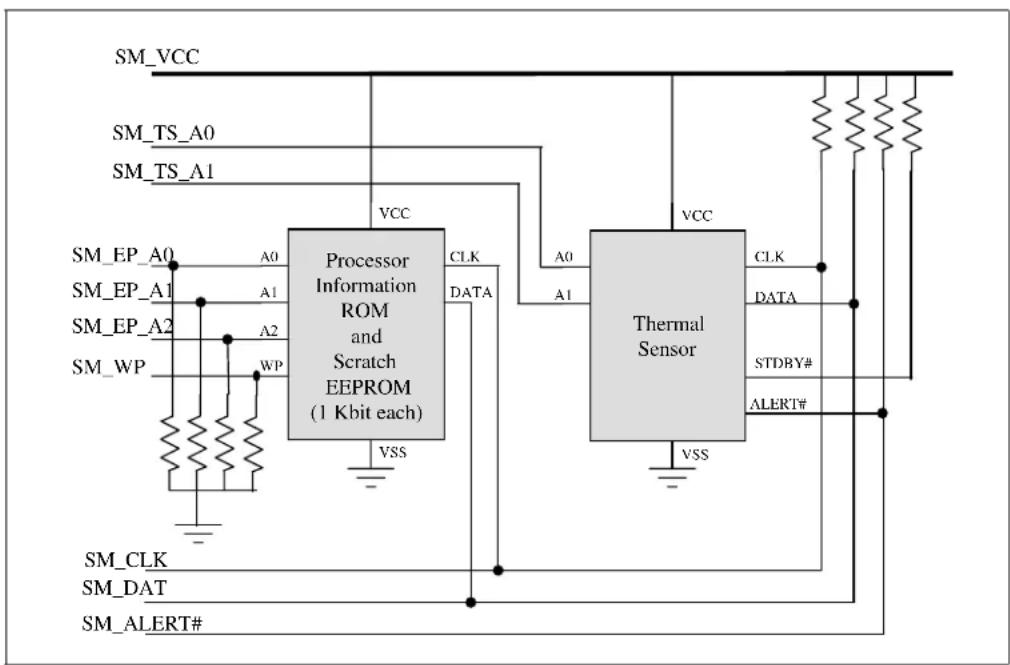
flowchart
graph TD
    A["SM_VCC"] --> B["Processor Information ROM and Scratch EEPROM (1 Kbit each)"]
    C["SM_TS_A0"] --> B
    D["SM_TS_A1"] --> B
    E["SM_EP_A0"] --> B
    F["SM_EP_A1"] --> B
    G["SM_EP_A2"] --> B
    H["SM_WP"] --> B
    I["SM_CLK"] --> B
    J["SM_DAT"] --> B
    K["SM_ALERT#"] --> B
    B --> L["VSS"]
    M["A0"] --> N["CLK"]
    O["A1"] --> P["DATA"]
    Q["A2"] --> R["WP"]
    S["A0"] --> T["VCC"]
    U["A1"] --> V["VCC"]
    W["VSS"] --> X["Thermal Sensor"]
    Y["VSS"] --> Z["Thermal Sensor"]
    AA["CLK"] --> AB["DATA"]
    AC["STDBY#"] --> AD["ALERT#"]
    AE["ALERT#"] --> AF["ALERT#"]
NOTE: Actual implementation may vary. This figure is provided to offer a general understanding of the architecture. All SMBus pull-up and pull-down resistors are 10 kΩ and located on the processor.
7.4.1 Processor Information ROM (PIROM)
The lower half (128 bytes) of the SMBus memory component is an electrically programmed read-only memory with information about the processor. This information is permanently write-protected. Table 7-2 shows the data fields and formats provided in the Processor Information ROM (PIROM). This is PIROM data format revision 2 (Offset 00). Fields which have changed for this revision are marked in italics in Table 7-2.
Table 7-2. Processor Information ROM Format (Sheet 1 of 3)
| Offset/Section | # of Bits | Function Notes | |
| Header: | |||
| 00h 8 Data Format Revision Two 4-bit hex digits | |||
| 01 - 02h 16 EEPROM M Size Size in bytes (MSB first) | |||
| 03h 8 Processor Data Address Byte pointer, 00h if not present | |||
| 04h | 8 Processor Core Data Address | Byte pointer, 00h if not present | |
| 05h 8 L3 Cache Data Address Byte pointer, 00h if not present | |||
| 06h 8 Package Data Address | Byte pointer, 00h if not present | ||
| 07h 8 Part Number Data Address | Byte pointer, 00h if not present | ||
| 08h | 8 Thermal Reference Data Address | Byte pointer, 00h if not present | |
| 09h 8 Feature Data Address | Byte pointer, 00h if not present | ||
| 0Ah 8 Other Data Address | Byte pointer, 00h if not present | ||
| 0Bh 16 | Reserved | Reserved | |
| 0Dh 8 | Checksum | 1 byte checksum | |
| Processor Data: | |||
| 0E - 13h | 48 | S-spec/QDF Number | Six 8-bit ASCII characters |
| 14h | 6 | Reserved | Reserved (most significant bits) |
| 2 | Sample/Production | 00b = Sample only, 01-11b = Production | |
| 15h 8 | Checksum | 1 byte checksum | |
| Processor Core Data: | |||
| 16 - 17h 2 | Processor Core Type | From CPUID | |
| 4 | Processor Core Family | From CPUID | |
| 4 | Processor Core Model | From CPUID | |
| 4 | Processor Core Stepping | From CPUID | |
| 2 | Reserved | Reserved for future use | |
| 18 - 19h 16 | Reserved | Reserved for future use | |
| 1A - 1Bh | 16 | Front Side Bus Speed | 16-bit hexadecimal number (in MHz) |
| 1Ch | 2 | Multiprocessor Support | 00b = UP,01b = DP,10b = RSVD,11b = MP |
| 6 | Reserved | Reserved | |
| 1D - 1Eh | 16 | Maximum Core Frequency | 16-bit hexadecimal number (in MHz) |
| 1F - 20h 16 | Max Processor Core VID | Max V CC requested by VID outputs in mV | |
| 21 - 22h 16 | Core Voltage, Minimum | Minimum processor DC V CC spec in mV | |
| 23h 8 | T CASE Maximum | Maximum case temperature spec in °C | |
| 24h 8 | Checksum | 1 byte checksum | |
Table 7-2. Processor Information ROM Format (Sheet 2 of 3)
| Offset/Section | # of Bits | Function | Notes |
| Cache Data: | |||
| 25 - 26h | 16 Reserved | Reserved for future use | |
| 27 - 28h | 16 L2 Cache Size per core | 16-bit hexadecimal number (in KB) | |
| 29 - 2Ah | 16 L3 Cache Size | 16-bit hexadecimal number (in KB). | |
| 2B - 2Ch | 16 Processor Cache VID | 16-bit hexadecimal Vcache value requested by CVID output (in mV). | |
| 2D - 2Eh | 16 Cache Voltage, Minimum | 16-bit hexadecimal Vcache value Minimum Processor DC Cache Voltage in (in mV). | |
| 2F - 30h | 16 Reserved | Reserved | |
| 31h | 8 Checksum | 1 byte checksum | |
| Package Data: | |||
| 32 - 35h | 32 | Package Revision | Four 8-bit ASCII characters |
| 36h | 8 | Reserved Reserved for future use | |
| 37h | 8 Checksum | 1 byte checksum | |
| Part Number Data: | |||
| 38 - 3Eh | 56 Processor Part Number Seven | 8-bit ASCII characters | |
| 3F - 4Ch | 112 | Reserved | Reserved |
| 4D - 54h | 64 | Processor Electronic Signature | 64-bit identification number |
| 55 - 6Eh | 208 | Reserved | Reserved |
| 6Fh | 8 Checksum | 1 byte checksum | |
| Thermal Ref. Data: | |||
| 70h | 8 | Reserved | Reserved |
| 71 - 72h | 16 Reserved | Reserved | |
| 73h | 8 Checksum | 1 byte checksum | |
| Feature Data: | |||
| 74 - 77h | 32 | Processor Core Feature Flags | From CPUID function 1, EDX contents |
| 78h | 8 Processor Feature Flags [7] = Multi-Core | ||
| 8 Processor Thread and Core Information | [7:4] = Reserved[3:2] = Number of cores[1:0] = Number of threads per core | ||
Table 7-2. Processor Information ROM Format (Sheet 3 of 3)
| Offset/Section | # of Bits | Function | Notes |
| 7Ah | 8 Additional ProcessorFeature Flags | [7] = Reserved[6] = Reserved[5] = Enhanced Halt State[4] = Intel® Virtualization Technology[3] = Execute Disable[2] = Intel® 64 architecture[1] = Thermal Monitor 2[0] = Enhanced Intel SpeedStep®Technology | |
| 7B-7Ch | 16 Thermal Adjustment Factors(Pending) | [15:8] Measurement Correction Factor[7:0] Temperature Target | |
| 7D- 7Eh | 16 Reserved Reserved | ||
| 7Fh | 8 Checksum 1 byte checksum | ||
7.4.2 Scratch EEPROM
Also available in the memory component on the processor SMBus is an EEPROM which may be used for other data at the system or processor vendor's discretion. The data in this EEPROM, once programmed, can be write-protected by asserting the active-high SM_WP signal. This signal has a weak pull-down (10 kΩ) to allow the EEPROM to be programmed in systems with no implementation of this signal. The Scratch EEPROM resides in the upper half of the memory component (addresses 80 - FFh). The lower half comprises the Processor Information ROM (addresses 00 - 7Fh), which is permanently write-protected by Intel.
7.4.3 PIROM and Scratch EEPROM Supported SMBus Transactions
The Processor Information ROM (PIROM) responds to two SMBus packet types: Read Byte and Write Byte. However, since the PIROM is write-protected, it will acknowledge a Write Byte command but ignore the data. The Scratch EEPROM responds to Read Byte and Write Byte commands. Table 7-3 diagrams the Read Byte command. Table 7-4 diagrams the Write Byte command. Following a write cycle to the scratch ROM, software must allow a minimum of 10 ms before accessing either ROM of the processor.
In the tables, 'S' represents the SMBus start bit, 'P' represents a stop bit, 'R' represents a read bit, 'W' represents a write bit, 'A' represents an acknowledge (ACK), and '///' represents a negative acknowledge (NACK). The shaded bits are transmitted by the Processor Information ROM or Scratch EEPROM, and the bits that aren't shaded are transmitted by the SMBus host controller. In the tables, the data addresses indicate 8 bits. The SMBus host controller should transmit 8 bits with the most significant bit indicating which section of the EEPROM is to be addressed: the Processor Information ROM (MSB = 0) or the Scratch EEPROM (MSB = 1).
Table 7-3. Read Byte SMBus Packet
| S | Slave Address | Write | A | Command Code | A | S | Slave Address | Read | A | Data | /// | P |
| 1 | 7-bits | 1 | 1 | 8-bits | 1 | 1 | 7-bits | 1 | 1 | 8-bits | 1 | 1 |
Table 7-4. Write Byte SMBus Packet
| S | Slave Address | Write | A | Command Code | A | Data | A | P |
| 1 | 7 - | b | 1 | 8 t - s | b | i 1 |
t
s
7.4.4 SMBus Thermal Sensor
The processor's SMBus thermal sensor provides a means of acquiring thermal data from the processor. The thermal sensor is composed of control logic, SMBus interface logic, precision analog-to-digital converters, and precision current sources. The sensor drives a small current through the p-n junction of a thermal diode located on each processor core. The forward bias voltage generated across the thermal diode is sensed and the precision A/D converter derives a single byte of thermal reference data, or a “thermal byte reading.” The nominal precision of the least significant bit of a thermal byte is 1° Celsius.
The processor incorporates the SMBus thermal sensor onto the processor package consistent with past members of the Intel Xeon processor family. Upper and lower thermal reference thresholds for each core can be individually programmed for the SMBus thermal sensor. Comparator circuits sample the register where the single byte of thermal data for each core (thermal byte reading) is stored. These circuits compare the single-byte result against programmable threshold bytes. If enabled, the alert signal on the processor SMBus (SM_ALERT#) will be asserted when the sensor detects that either core's threshold is reached or crossed. Analysis of SMBus thermal sensor data may be useful in detecting changes in the system environment that may require attention. Note that sensor readings from different cores can vary significantly and must all be monitored.
The SMBus thermal sensor feature in the processor cannot be used to measure T_CASE . The T_CASE specification in Section 6 must be met regardless of the reading of the processor's thermal sensor in order to ensure adequate cooling for the entire processor. The SMBus thermal sensor feature is only available while V_CC and SM_VCC are at valid levels and the processor is not in a low-power state.
7.4.5 Thermal Sensor Supported SMBus Transactions
The thermal sensor responds to five of the SMBus packet types: Write Byte, Read Byte, Send Byte, Receive Byte, and Alert Response Address (ARA). The Send Byte packet can be used for sending one-shot commands. The Receive Byte packet accesses the register commanded by the last Read Byte packet and can be used to continuously read from a register. If a Receive Byte packet was preceded by a Write Byte or send Byte packet more recently than a Read Byte packet, then the behavior is undefined. Table 7-5 through Table 7-9 diagram the five packet types. In these figures, 'S' represents the SMBus start bit, 'P' represents a stop bit, 'Ack' represents an acknowledge, and '///' represents a negative acknowledge (NACK). The shaded bits are transmitted by the thermal sensor, and the bits that aren't shaded are transmitted by the SMBus host controller. Table 7-10 shows the encoding of the command byte.
Table 7-5. Write Byte SMBus Packet
| S | Slave Address | Write | Ack | Command Code | Ack | Data | Ack | P |
| 1 | 7-bits | 0 | 1 | 8-bits | 1 | 8-bits | 1 | 1 |
Table 7-6. Read Byte SMBus Packet
| S | Slave Address | Write Ack | Command Code | Ack S | Slave Address | Read | Ack Data /// P | ||||||
| 1 | 7 - | b | i | 1 t | 8bits | 10 | 1 | 7-bits | 1 | 1 | 8-bits | 1 | 1 |
| S | Slave Address | Write | Ack | Command Code | Ack | P |
| 1 | 7-bits | 0 | 1 | 8-bits | 1 | 1 |
Table 7-8. Receive Byte SMBus Packet
| S | Slave Address | Read | Ack | Data | /// | P |
| 1 | 7-bits | 1 | 1 | 8-bits | 1 | 1 |
Table 7-9. ARA SMBus Packet
| S | ARA | Read | Ack | Address | /// | P |
| 1 | 0001 100 | 1 | 1 | Device Address _1 | 1 | 1 |
NOTES:
- This is an 8-bit field. The device which sent the alert will respond to the ARA Packet with its address in the seven most significant bits. The least significant bit is undefined and may return as a '1' or '0'. See Section 7.4.8 for details on the Thermal Sensor Device addressing.
- The shaded bits are transmitted by the thermal sensor, and the bits that aren't shaded are transmitted by the SMBus host controller.
Table 7-10. SMBus Thermal Sensor Command Byte Assignments
| Register Command R/W Reset State | |||
| RESERVED^2 | 00h N/A | RESERVED | |
| Ch. 1 Temp. Value1 | 01h R 0000 | 0000 | |
| Status Register 1 02h R | Undefined | ||
| Configuration Register | 03h R 0000 | 0000 | |
| Conversion Rate Register | 04h R | 0000 | 0111 |
| RESERVED^2 | 05h - 06h | N/A | RESERVED |
| Ch. 1 Temp. High Limit1 | 07h R 0101 | 0101 | |
| Ch. 1 Temp. Low Limit1 | 08h R 0000 | 0000 | |
| Configuration Register 1 | 09h | W | 0000 0000 |
| Conversion Rate Register | 0Ah | W | 0000 0111 |
| RESERVED^2 | 0Bh - 0Ch | N/A | RESERVED |
| Ch. 1 Temp. High Limit1 | 0Dh | W | 0101 0101 |
| Ch. 1 Temp. Low Limit1 | 0Eh | W | 0000 0000 |
| One-shot | 0Fh | W | N/A |
| RESERVED^2 | 10h N/A | RESERVED | |
| Ch. 1 Temp. Offset1 | 11h | R/W | 0000 0000 |
| RESERVED^2 | 12h - 22h | N/A | RESERVED |
| Status Register 2 23h R 0000 | 0000 | ||
| RESERVED^2 | 24h - 29h | N/A | RESERVED |
| Ch. 2 Temp. Value | 30h R 0000 | 0000 | |
| Ch. 2 Temp. High Limit | 31h | R/W | 0101 01010 |
| Ch. 2 Temp. Low Limit | 32h | R/W | 0000 0000 |
| RESERVED^2 | 33h R 0000 | 0000 | |
| Ch. 2 Temp. Offset | 34h R/W | 0000 | 0000 |
| RESERVED^2 | 35h - FEh | N/A | RESERVED |
| Die Revision Code3 | FFh | R 1001 | XXXX |
NOTES:
- Bit 3 of Configuration register 1 must be set to 0 (default value is 0)
- Writing to RESERVED bits may cause unexpected results. RESERVED bits that must be correctly programmed are identified in the register definitions in the following section. Reading from RESERVED bits will return unknown values.
- The 4 least significant bits of the thermal sensor die revision code may change and should not be used for identification
- Ch. 1 limit registers have a separate 7-bit read and write address while channel 2 limit registers have the same 7-bit address for read and write.
All of the commands in Table 7-10 are for reading or writing registers in the SMBus thermal sensor, except the one-shot register (0Fh). The one-shot command forces the start of a new conversion cycle. If a conversion is in progress when the one-shot command is received, then the command is ignored. If the thermal sensor is in stand-by mode when the one-shot command is received, a conversion is performed and the sensor returns to stand-by mode. The one-shot command is not supported when the thermal sensor is in auto-convert mode.
Note: Writing to a read-command register or reading from a write-command register will produce invalid results.
The default command after reset is to a reserved value (00h). After reset, Receive Byte SMBus packets will return invalid data until another command is sent to the thermal sensor.
7.4.6 SMBus Thermal Sensor Registers
7.4.6.1 Temperature Value Registers
Once the SMBus thermal sensor reads a processor thermal diode, it performs an analog to digital conversion and stores the data in a temperature value register. The supported range is 0 to +127 decimal and is expressed as an eight-bit number representing temperature in degrees Celsius. This eight-bit value consists of seven bits of data and a sign bit (MSB) where the sign is always positive (sign = 0) and is shown in Table 7-7. The values shown are also used to program the Thermal Limit Registers.
The values of these registers should be treated as saturating values. Values above 127 are represented at 127 decimal, and values of zero and below may be represented as 0 to -127 decimal. If the device returns a value where the sign bit is set (1) and the data is 000_0000 through 111_1110, the temperature should be interpreted as 0° Celsius.
Table 7-11. Temperature Value Register Encoding
| Temperature (°C) | Register Value (binary) |
| +127 0 111 1111 | |
| +126 0 111 1110 | |
| +100 0 110 0100 | |
| +50 0 011 0010 | |
| +25 0 001 1001 | |
| +1 0 000 0001 | |
| 0 0 000 0000 |
7.4.6.2 Thermal Limit Registers
The SMBus thermal sensor has high and low Thermal Limit Registers for each channel. These registers allow the user to define high and low limits for the processor core thermal diode readings. The encoding for these registers is the same as for the thermal reference registers shown in Table 7-7. If either processor thermal diode reading equals or exceeds one of these limits, then the alarm bit (R1HIGH, R1LOW, R2HIGH, or R2LOW) in the Thermal Sensor Status Register is triggered.
7.4.6.3 Status Registers
The Status Registers shown in Table 7-12 and Table 7-13 indicates which, if any, thermal value thresholds for the processor core thermal diode have been exceeded. It also indicates whether a conversion is in progress or an open circuit has been detected in either processor core thermal diode connection. Once set, alarm bits stay set until they are cleared by a Status Register read. A successful read to the Status Register will clear any alarm bits that may have been set (unless the
alarm condition persists). If the SM_ALERT# signal is enabled via the Thermal Sensor Configuration Register and a thermal diode threshold is exceeded, an alert will be sent to the platform via the SM_ALERT# signal.
Table 7-12. SMBus Thermal Sensor Status Register 1
| Bit Name | Reset State Function | ||
| 7 (MSB) | BUSY N/A If set, indicates that the device's converter is busy. | ||
| 6 | RESERVED RESERVED | Reserved for future use. | |
| 5 | RESERVED RESERVED | Reserved for future use. | |
| 4 | R1HIGH | 0 | If set, indicates the processor core 1 thermal diode high temperature alarm has activated. |
| 3 | R1LOW | 0 | If set, indicates the processor core 1 thermal diode low temperature alarm has activated. |
| 2 | R1OPEN | 0 | If set, indicates an open fault in the connection to the processor core 1 diode. |
| 1 | RESERVED RESERVED | Reserved for future use. | |
| 0 (LSB) | RESERVED RESERVED | Reserved for future use. | |
Table 7-13. SMBus Thermal Sensor Status Register 2
| Bit Name | Reset State Function | ||
| 7 (MSB) | RESERVED | Reserved Reserved for future use. | |
| 6 RESERVED | Reserved reserved | Reserved for future use. | |
| 5 RESERVED | Reserved reserved | Reserved for future use. | |
| 4 | R2HIGH | 0 | If set, indicates the processor core 2 thermal diode high temperature alarm has activated. |
| 3 | R2LOW | 0 | If set, indicates the processor core 2 thermal diode low temperature alarm has activated. |
| 2 | R2OPEN | 0 | If set, indicates an open fault in the connection to the processor core 2 diode. |
| 1 RESERVED | Reserved reserved | Reserved for future use. | |
| 0 (LSB) | ALERT | 0 | If set, indicates the ALERT pin has been asserted low. This bit gets reset when the ALERT output gets reset. |
7.4.6.4 Configuration Register
The Configuration Register controls several functions of the temperature sensor such as ALERT# masking, stand-by mode, and others. Table 7-14 and Table 7-11 shows the bit definitions of the Configuration Registers.
Table 7-14. SMBus Thermal Sensor Configuration Register (Sheet 1 of 2)
| Bit Name Reset State Function | |||
| 7 (MSB) | MASK | 0 | Mask SM_ALERT# bit. Clear the bit to allow interrupts via SM_ALERT# and allow the thermal sensor to respond to the ARA command when an alarm is active. Set the bit to disable interrupt mode. The bit is not used to clear the state of the SM_ALERT# output. An ARA command may not be recognized if the mask is enabled. |
Table 7-14. SMBus Thermal Sensor Configuration Register (Sheet 2 of 2)
| Bit | Name | Reset State | Function |
| 6 RUN | STOP 0 Stand-by mode control bit. If set | the device immediately stops converting, and enters stand-by mode. It will perform new temperature measurements when a one-shot is performed. If cleared the device automatically updates on a timed basis. | |
| 5 AL/TH | 0 This bit selects the function of pin 13. | Default = 0 = ALERT. Always set this bit to 0. | |
| 4 RESERVED | RESERVED | Reserved for future use. | |
| 3 Remote | 1/2 0 Setting this bit to 1 enables the | user to read the remote2 values from the remote 1 registers. Default = 0 = Read remote 1 values from the remote 1 registers. Always set this bit to 0. | |
| 2 Temp | Range 0 Setting this bit to 1 enables the | extended temperature measurement range (-50 °C to +150 °C). Default = 0 = (0 °C to 127 °C). Always set this bit to 0. | |
| 1 | Mask R1 | 0 | Setting this bit to 1 masks ALERTS due to the processor core 1 temperature exceeding a programmed limit. Default = 0. Always set this bit to 0. |
| 0 | Mask R2 | 0 | Setting this bit to 1 masks ALERTS due to the processor core 2 temperature exceeding a programmed limit. Default = 0. Always set this bit to 0. |
7.4.6.5 Conversion Rate Register
The contents of the Conversion Rate Registers determine the nominal rate at which analog-to-digital conversions happen when the SMBus thermal sensor is in auto-convert mode. There are two Conversion Rate Registers: address 04h for reading the conversion rate value; and address 0Ah for writing the value. Table 7-15 shows the mapping between Conversion Rate Register values and the conversion rate. As indicated in Table 7-10, the Conversion Rate Register is set to its default state of 1000b (16 Hz nominally) when the thermal sensor is powered up. There is a ±30% error tolerance between the conversion rate indicated in the conversion rate register and the actual conversion rate.
Table 7-15. SMBus Thermal Sensor Conversion Rate Register (Sheet 1 of 2)
| Bit | Name | Reset State | Function |
| 7 (MSB) | Averaging | 0 | Setting this bit to 1 disables averaging of the temperature measurements at the slower conversion rates. Default = 0 = Averaging enabled. |
| 6 RESERVED RESERVED | Reserved for future use. | ||
Table 7-15. SMBus Thermal Sensor Conversion Rate Register (Sheet 2 of 2)
| Bit Name | Reset State | Function |
| 5:4 Channel Selector 00 These bits are used to select the temperature measurement channels.00 = Round robin01 = Local Temperature10 = Remote 1 Temperature11 = Remote 2 TemperatureDefault = 00. Always set these bits to 00 | ||
| 3:0 Conversion Rates 1000 These bits determine how often the temperature sensor measures each temperature channel.Bit encoding = Conversions / sec0000 = 0.06250001 = 0.1250010 = 0.250011 = 0.50100 = 10101 = 20110 = 40111 = 81000 = 16 = default1001 = 321010 = Continuous Measurements | ||
7.4.7 SMBus Thermal Sensor Alert Interrupt
The SMBus thermal sensor located on the processor includes the ability to interrupt the SMBus when a fault condition exists. The fault conditions consist of:
- A processor thermal diode value measurement that exceeds a user-defined high or low threshold programmed into the Command Register; or
- Disconnection of the processor thermal diode from the thermal sensor.
The interrupt can be enabled and disabled via the thermal sensor Configuration Register and is delivered to the system board via the SM_ALERT# open drain output. Once latched, the SM_ALERT# should only be cleared by reading the Alert Response byte from the Alert Response Address of the thermal sensor. The Alert Response Address is a special slave address shown in Table 7-9. The SM_ALERT# will be cleared once the SMBus master device reads the slave ARA unless the fault condition persists. Reading the Status Register or setting the mask bit within the Configuration Register does not clear the interrupt.
7.4.8 SMBus Device Addressing
Of the addresses broadcast across the SMBus, the memory component claims those of the form "1010XXXZb". The "XXX" bits are defined by pull-up and pull-down resistors on the system baseboard. These address pins are pulled down weakly (10 kΩ) on the processor substrate to ensure that the memory components are in a known state in systems which do not support the SMBus (or only support a partial implementation). The "Z" bit is the read/write bit for the serial bus transaction.
The thermal sensor internally decodes one of three upper address patterns from the bus of the form "0011XXXZb", "1001XXXZb", or "0101XXXZb". The device's addressing, as implemented, uses the SM_TS_A[1:0] pins in either the HI, LO, or Hi-Z state. Therefore, the thermal sensor supports nine unique addresses. To set either pin for the Hi-Z state, the pin must be left floating. As before, the "Z" bit is the read/write bit for the serial transaction.
Note that addresses of the form “0000XXXXb” are Reserved and should not be generated by an SMBus master. The thermal sensor samples and latches the SM_TS_A[1:0] signals at power-up and at the starting point of every conversion. System designers should ensure that these signals are at valid V_IH , V_IL , or floating input levels prior to or while the thermal sensor’s SM_VCC supply powers up. This should be done by pulling the pins to SM_VCC or V_SS via a 1 kΩ or smaller resistor, or leaving the pins floating to achieve the Hi-Z state. If the system designer wants to drive the SM_TS_A[1:0] pins with logic, the designer must still ensure that the pins are at valid input levels prior to or while the SM_VCC supply ramps up. The system designer must also ensure that their particular implementation does not add excessive capacitance to the address inputs. Excess capacitance at the address inputs may cause address recognition problems. Refer to the appropriate platform design guide document.
Figure 7-2 shows a logical diagram of the pin connections. Table 7-16 and Table 7-17 describe the address pin connections and how they affect the addressing of the devices.
Table 7-16. Thermal Sensor SMBus Addressing
| Device Select | Address (Hex) | 8-bit Address Word on Serial Bus | |
| SM_TS_A1 SM_TS_A0 b[7:0] | |||
| 0 | 0 | 3Xh 0011000Xb | |
| 0 | Z^2 | 0011001Xb | |
| 0 | 1 | 0011010Xb | |
| Z^2 | 0 | 5Xh 0101001Xb | |
| Z^2 | Z^2 | 0101010Xb | |
| Z^2 | 1 | 0101011Xb | |
| 1 | 0 | 9Xh 1001100Xb | |
| 1 | Z^2 | 1001101Xb | |
| 1 | 1 | 1001110Xb | |
NOTES:
- Upper address bits are decoded in conjunction with the device select pins.
- A tri-state or "Z" state on this pin is achieved by leaving this pin unconnected.
Note: System management software must be aware of the processor dependent addresses for the thermal sensor.
Table 7-17. Memory Device SMBus Addressing
| Address (Hex) | Upper Address1 | Device Select R/W | |||
| bits 7-4 | SM_EP_A2 bit 3 | SM_EP_A1 bit 2 | SM_EP_A0 bit 1 | bit 0 | |
| A0h/A1h 10 | 10 0 0 0 X | ||||
| A2h/A3h 10 | 10 0 0 1 X | ||||
| A4h/A5h 10 | 10 0 1 0 X | ||||
| A6h/A7h 10 | 10 0 1 1 X | ||||
| A8h/A9h 10 | 10 1 0 0 X | ||||
| AAh/ABh 10 | 10 1 0 1 X | ||||
| ACh/ADh 10 | 10 1 1 0 X | ||||
| AEh/AFh 10 | 10 1 1 1 X | ||||
NOTE:
- This addressing scheme will support up to 8 processors on a single SMBus.
7.4.9 Managing Data in the PIROM
The PIROM consists of the following sections:
- Header
- Processor Data
- Processor Core Data
- Cache Data
- Package Data
- Part Number Data
• Thermal Reference Data - Feature Data
- Other Data
Details on each of these sections are described below.
Note: Reserved fields or bits SHOULD be programmed to zeros. However, OEMs should not rely on this model.
7.4.9.1 Header
To maintain backward compatibility, the Header defines the starting address for each subsequent section of the PIROM. Software should check for the offset before reading data from a particular section of the ROM.
Example: Code looking for the cache data of a processor would read offset 05h to find a value of 25h. 25h is the first address within the 'Cache Data' section of the PIROM.
The Header also includes the data format revision at offset 0h and the EEPROM size (formatted in hex bytes) at offset 01-02h. The data format revision is used whenever fields within the PIROM are redefined. Normally the revision would begin at a value of 1. If a field, or bit assignment within a field, is changed such that software needs to discern between the old and new definition, then the data format revision field should be incremented.
The EEPROM size provides the size of the PIROM in hex bytes. The PIROM is 128 bytes; thus, offset 01 - 02h would be programmed to 80h.
7.4.9.2 Processor Data
This section contains two pieces of data:
• The S-spec/QDF of the part in ASCII format
• (1) 2-bit field to declare if the part is a pre-production sample or a production unit
The S-spec/QDF field is six ASCII characters wide and is programmed with the same S-spec/QDF value as marked on the processor. If the value is less than six characters in length, leading spaces (20h) are programmed in this field.
Example: A processor with a QDF mark of QEU5 contains the following in field 0E-13h: 20, 20, 51, 45, 55, 35h.
This data consists of two blanks at 0Eh and 0Fh followed by the ASCII codes for QEU5 in locations 10 - 13h.
Offset 14h contains the sample/production field, which is a two-bit field and is LSB aligned. All Q-spec material will use a value of 00b. All S-spec material will use a value of 01b. All other values are reserved.
Example: A processor with a Qxxx mark (engineering sample) will have offset 14h set to 00b. A processor with an Sxxxx mark (production unit) will use 01b at offset 14h.
7.4.9.3 Processor Core Data
This section contains core silicon-related data.
7.4.9.3.1 CPUID
The CPUID field is a copy of the results in EAX[13:0] from Function 1 of the CPUID instruction.
Note: The field is not aligned on a byte boundary since the first two bits of the offset are reserved. Thus, the data must be shifted right by two in order to obtain the same results.
Example: The CPUID of a C-1 stepping Intel Xeon processor with 512 KB L2 cache is 0F27h. The value programmed into offset 16 - 17h of the PIROM is 3C9Ch.
Note: The first two bits of the PIROM are reserved, as highlighted in the example below.
CPUID instruction results 0000 1111 0010 0111 (0F27h)
PIROM content 0011 1100 1001 1100 (3C9Ch)
7.4.9.3.2 Front Side Bus Frequency
Offset 1A - 1Bh provides FSB frequency information. Systems may need to read this offset to decide if all installed processors support the same FSB speed. Because the Intel NetBurst ^® microarchitecture bus is described as a 4x data bus, the frequency given in this field is currently 667 MHz. The data provided is the speed, rounded to a whole number, and reflected in hex.
Example: The Dual-Core Intel Xeon processor 7000 series supports a 667 MHz FSB. Therefore, offset 1A - 1Bh has a value of 029Bh.
Offset 1Ch has 2 bits defined for representing the supported number of physical processors on the bus. These two bits are MSB aligned where 00b equates to single-processor operation, 01b is a dual-processor operation, and 11b represents multi-processor operation. Normally, only values of 01 and 11b are used. The remaining six bits in this field are reserved for the future use.
7.4.9.3.4 Maximum Core Frequency
Offset 1D - 1Eh provides the maximum core frequency for the processor. The frequency should equate to the markings on the processor and/or the QDF/S-spec speed even if the parts are not limited or locked to the intended speed. Format of this field is in MHz, rounded to a whole number, and encoded in hex format.
Example: A 2.8 GHz processor will have a value of 0AF0h, which equates to 2800 decimal.
7.4.9.3.5 Core Voltage
There are two areas defined in the PIROM for the core voltages associated with the processor. Offset 1F - 20h is the Processor Core VID (Voltage Identification) field and contains the voltage requested via the VID pins. In the case of the Dual-Core Intel Xeon processor 7000 series, this is 1.3875 V. This field, rounded to the next thousandth, is in mV and is reflected in hex. This data is also in Table 2-8. Some systems read this offset to determine if all processors support the same default VID setting.
Minimum core voltage is reflected in offset 21 – 22h. This field is in mV and reflected in hex. The minimum VCC reflected in this field is the minimum allowable voltage assuming the FMB maximum current draw.
Note: The minimum core voltage value in offset 21 – 22h is a single value that assumes the FMB maximum current draw. Refer to Table 2-8. for the actual minimum core voltage specifications based on actual real-time current draw.
Example: The specifications for a Dual-Core Intel Xeon processor 7000 series at FMB are 1.4125 V VID and 1.200 V minimum voltage. Offset 1F - 20h would contain 585h (1413 decimal) and offset 21 - 22h would contain 4B0h (1200 decimal).
7.4.9.3.6 T CASE Maximum
The last field within Processor Core Data is the T_CASE Maximum field. The field reflects temperature in degrees Celsius in hex format. This data can be found in the Table 6-1. In the case of the Dual-Core Intel Xeon processor 7000 series, the thermal specifications are specified at the case (IHS).
7.4.9.4 Cache Data
This section contains cache-related data.
7.4.9.4.1 L2 Cache Size
Offset 27 - 28h is the L2 cache size field. The field reflects the size of the level two cache for each core in kilobytes.
Example: The Dual-Core Intel Xeon processor 7000 series may have a 2 MB (2048 KB) L2 cache per core. Thus, offset 27 - 28h will contain 800h.
7.4.9.4.2 L3 Cache Size
Offset 29 - 2Ah is the L3 cache size field. The field reflects the size of the level three cache in kilobytes.
Example: The Dual-Core Intel Xeon processor 7000 series does not have an L3 cache per core. Thus, offset 29 - 2Ah will contain 0h.
7.4.9.4.3 Cache Voltage
There are two areas defined in the PIROM for the L3 cache voltages associated with the processor. Offset 2B - 2Ch is the Processor Cache VID (Cache Voltage Identification), or CVID, field and contains the voltage requested via the CVID pins. Because the Dual-Core Intel Xeon processor 7000 series does not have an L3 cache, this field is set to 0h. This field is in mV and is reflected in hex. Some systems read this offset to determine if all processors support the same default CVID setting.
Minimum L3 cache voltage specifications are reflected in offset 2D - 2Eh. This field is in mV and reflected in hex. For processors that follow a load line DC specification, the minimum V_CACHE reflected in this field should reflect the minimum allowable voltage at maximum current.
Example: Since the Dual-Core Intel Xeon processor 7000 series does not have an L3 cache, offset 2B - 2Ch would contain 0h and offset 2D - 2Eh would contain 0h.
7.4.9.5 Package Data
This section describes the package revision location at offset 32 - 35h. This field tracks the highest level revision. It is provided in ASCII format of four characters (8 bits x 4 characters = 32 bits). The package is documented as 1.0, 2.0, etc. Because this only consumes three ASCII characters, a leading space is provided in the data field.
Example: The C-1 stepping of the Intel Xeon processor with 512 KB L2 cache is packaged in the 603-pin micro-PGA interposer with 31 mm OLGA package and utilizes the second revision of this package. Thus, at offset 32-35h the data is a space followed by 2.0. In hex, this would be 20, 32, 2E, 30.
7.4.9.6 Part Number Data
This section provides traceability. There are 208 available bytes in this section for future use.
7.4.9.6.1 Processor Part Number
Offset 38 - 3Eh contains seven ASCII characters reflecting the Intel part number for the processor. This information is typically marked on the outside of the processor. If the part number is less than 7 characters, a leading space is inserted into the value. The part number should match the information found in the marking specification found in Section 3.
Example: The Intel Xeon processor with 512 KB L2 cache (533 MHz FSB) has a part number of 80532KE. Thus, the data found at offset 38 - 3Eh is 38, 30, 35, 33, 32, 4B, 45.
7.4.9.6.2 Processor Electronic Signature
Offset 4D - 54h contains a 64-bit identification number. Intel does not guarantee that each processor will have a unique value in this field.
7.4.9.7 Feature Data
This section provides information on key features that the platform may need to understand without powering on the processor.
7.4.9.7.1 Processor Core Feature Flags
Offset 74 - 77h contains a copy of results in EDX[31:0] from Function 1 of the CPUID instruction. These details provide instruction and feature support by product family. A decode of these bits is found in the Prescott, Nocona and Potomac Processor BIOS Writer's Guide (BWG) or the AP-485 Intel® Processor Identification and CPUID Instruction application note.
7.4.9.7.2 Processor Feature Flags
Offset 78h provides feature information for the processor. This field is defined as follows:
Table 7-18. Offset 78h Definitions
| Bit Definition | |
| 7 Multi-Core (set if the processor is a dual core processor) | |
| 6 Serial signature (set if there is a serial signature at offset 4D - 54h) | |
| 5 Electronic signature present (set if there is a electronic signature at 4D - 54h) | |
| 4 Thermal Sense Device present (set if an SMBus thermal sensor on package) | |
| 3 | R e s e r v e d |
| 2 OEM EEPROM present (set if there is a scratch ROM at offset 80 - FFh) | |
| 1 Core VID present (set if there is a VID provided by the processor) | |
| 0 | R e s e r v e d |
Bits are set when a feature is present, and cleared when they are not.
7.4.9.7.3 Processor Thread and Core Information
Offset 79h provides information regarding the number of cores and threads on the processor.
Table 7-19. Offset 79h Definitions (Sheet 1 of 2)
| Bits Definition |
| 7:4 Reserved |
Table 7-19. Offset 79h Definitions (Sheet 2 of 2)
| Bits Definition |
| 3:2 Number of cores |
| 1:0 Number of threads per core |
Example: The Dual-Core Intel Xeon processor 7000 series has two cores and two threads per core. Therefore, this register will have a value of 0Ah
7.4.9.7.4 Additional Processor Feature Flags
Offset 7Ah provides additional feature information for the processor. This field is defined as follows:
Table 7-20. Offset 7Ah Definitions
| Bit Definition | |
| 7:6 Reserved | |
| 5 Enhanced Halt State | |
| 4 Intel | ® Virtualization Technology |
| 3 Execute | Disable |
| 2 Intel | ® 64 |
| 1 Thermal | Monitor 2 |
| 0 Enhanced Intel Speed Step | ® Technology |
Bits are set when a feature is present, and cleared when they are not.
7.4.9.7.5 Thermal Adjustment Factors
Offsets 7B-7Ch provides information on thermal adjustment factors for the processor. This field and it's details are pending and will be updated in a future revision. The field is defined as follows:
Table 7-21. Offset 7Bh Definitions
| Bit Definition | |
| 15:8 | Measurement Correction Factor |
| 7:0 Temperature Target | |
7.4.9.8 Other Data
Addresses 7D - 7E are listed as reserved.
7.4.9.9 Checksums
The PIROM includes multiple checksums. Table 7-22 includes the checksum values for each section defined in the 128 byte ROM, except Other Data.
Table 7-22. 128 Byte ROM Checksum Values
| Section Checksum Address | |
| Header 0Dh | |
| Processor Data 15h | |
| Processor Core Data 24h | |
| Cache Data 31h | |
| Package Data 37h | |
| Part Number Data 6Fh | |
| Thermal Reference Data 73h | |
| Feature Data 7Fh | |
| Other Data None Defined | |
Checksums are automatically calculated and programmed by Intel. The first step in calculating the checksum is to add each byte from the field to the next subsequent byte. This result is then negated to provide the checksum.
Example: For a byte string of AA445Ch, the resulting checksum will be B6h.
$$ \mathrm{AA} = 1 0 1 0 1 0 1 0 4 4 = 0 1 0 0 0 1 0 0 5 \mathrm{C} = 0 1 0 1 1 0 0 $$
$$ \mathrm{AA} + 4 4 + 5 \mathrm{C} = 0 1 0 0 1 0 1 0 $$
Negate the sum: 10110101 +1 = 101101 (B6h)
Features
intel®
8 Boxed Processor Specifications
8.1 Introduction
The Dual-Core Intel Xeon processor 7000 series will be offered as an Intel boxed processor. Intel boxed processors are intended for system integrators who build systems from components available through distribution channels. The boxed thermal solution is under development and is subject to change. This section is meant to provide some insight into the current direction of the thermal solution. Future revisions may have solutions that differ from those discussed here.
The current thermal solution plan for the boxed Dual-Core Intel Xeon processor 7000 series is to include an unattached passive heatsink. This solution is currently targeted at chassis which are 3U and above in height.
This section documents baseboard and platform requirements for the thermal solution, supplied with the boxed Dual-Core Intel Xeon processor 7000 series. This section is particularly important to companies that design and manufacture baseboards, chassis and complete systems. Figure 8-1 shows the conceptual drawing of the boxed processor thermal solution.
Drawings in this section reflect only the specifications on the Intel boxed processor product. These dimensions should not be used as a generic keepout zone for all cooling solutions. It is the system designer's responsibility to consider their proprietary cooling solution when designing to the required keepout zone on their system platform and chassis.
Figure 8-1. Passive Dual-Core Intel® Xeon® Processor 7000 Series Thermal Solution (3U and Larger)
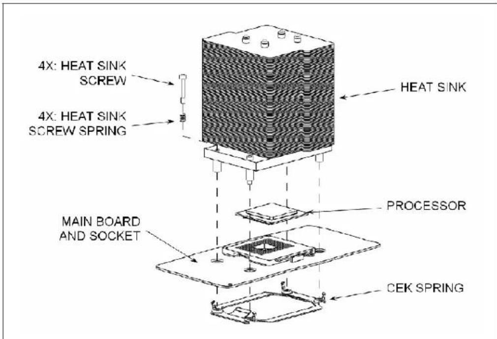
NOTE:
- The heatsink in this image is for reference only.
- This drawing shows the retention scheme for the boxed processor.
8.2 Mechanical Specifications
This section documents the mechanical specifications of the boxed processor passive heatsink.
8.2.1 Boxed Processor Heatsink Dimensions
The boxed processor is shipped with an unattached passive heatsink. Clearance is required around the heatsink to ensure unimpeded airflow for proper cooling. The physical space requirements and dimensions for the boxed processor and assembled heatsink are shown in the following figures.
Figure 8-2. Top Side Board Keepout Zones (Part 1)
![THIS DRAWING CONTAINS INTEL CORPORATION CONFIDENTIAL INFORMATION. IT IS DISCLOSED IN CONFIDENCE AND ITS CONTENTS WAY NOT BE DISCLOSED, REPRODUCED, DISPLATED OR MODIFIED, WITHOUT THE PRIOR WRITTEN CONSENT OF INTEL CORPORATION. NOTES: PRIMARY SIDE AIRFLOW (93.98) [3.100] HEATSINK DISASSEMBLY OUTLINE (88.9) [3.500] 29.21 [1.503] 4 TEST BOARD SHOWN FOR REFERENCE 4X Ø 10, 16⁺°0, 05 .0, 02 [ .400⁺°002 ] PROCESSOR MOUNTING THRU HOLES SOCKET PIN # 2.6 [ .496 ] 0 1.007 SOCKET PIN ROW IN LINE WITH MB HOLE 325° HEIGHT RESTRICTION LEGEND: .150° (3.8 MW) MAX COMPONENT HEIGHT RESTRICTION. HEATSINK AREA, .325° (8.26 MW) MAX COMPONENT HEIGHT RESTRICTION. HEATSINK DISASSEMBLY AREA, .325° (8.26 MW) MAX COMPONENT HEIGHT RESTRICTION. NO MOTHERBOARD COMPONENT PLACEMENT ALLOWED. .551° (4MM) MAX MOTHERBOARD COMPONENT HEIGHT RESTRICTION. CEK SPRING BOARD FINGER KEEPOUT, NO MOTHERBOARD COMPONENTS ALLOWED. MPGA604 SOCKET BOUNDARY FOR REFERENCE ONLY 81.28 [3.200] REVISION HISTORY ITEM: 14/02/02 DESCRIPTION: INTG DRAWN BY: ZON MEISON COLLENE SWN. DATE: 14/02/02 CHECKED BY: DATE APPROVED BY: DATE MATERIAL: X FINISH: P SCALE: NONE DO NOT SCALE DRAWING SHEET 1 OF 6 8 7 6 5 ↑ 4 3 2 1](/content/2026/05/1140870/images/738bb3859554531094ad308f41d2177a7e46a8ccb04f9b8ef4b02cc2683807b4.jpg)
Figure 8-3. Top Side Board Keepout Zones (Part 2)
![THIS DRAWING CONTAINS (Intel CORPORATION CONVECTUAL INFORMATION, IT IS DISCLOSE IN CONFERENCE AND ITS CONTENTS MAY NOT BE USED WITHOUT THE PRIOR WRITTEN CONSENT OFIntel CORPORATION) D C B LEGEND: .150° (3.81MM) MAX COMPONENT HEIGHT RESTRICTION. HEATSINK AREA, .325° (8.26 MM) MAX COMPONENT HEIGHT RESTRICTION. HEATSINK DISASSEMBLY AREA, .325° (8.26 MM) MAX COMPONENT HEIGHT RESTRICTION. NO MOTHERBOARD COMPONENT PLACEMENT ALLOWED. .351° (14MM) MAX MOTHERBOARD COMPONENT HEIGHT RESTRICTION. CEK SPRING BOARD FINGER KEEPOUT, NO MOTHERBOARD COMPONENTS ALLOWED. 22.86 [1.900] 20.32 [1.800] 12.7 [1.500] 8.26 [1.325] 8 [1.315] 0 [1.000] [2.25 [1.482] [2.7 [1.500] 25.4 [1.000] 25.86 [1.018] 46.1 [1.815] 46.26 [1.825] 50.8 [2.000] 58.42 [2.300] 50.95 [2.400] 4X Ø 10,16+0,05 -0,02 [400+002 001] PROCESSOR MOUNTING THRU HOLES PRIMARY SIDE INTL® 1270 WELDER COALDER BLOOD COMP 275 002 18:3 DRAWN CODE A75292 ISSN 15 DB-ALL-NAME DO NOT SCALE DRAWING SHEET 2 OF 4](/content/2026/05/1140870/images/2b05134581c2ebf2b2d8cf86007bd527cd30efc59c0a780b25f4c28df48ffc57.jpg)
Figure 8-4. Bottom Side Board Keepout Zones
![THIS DRAWING CONTAINS DETAIL CORPORATION CONFIDENTIAL INFORMATION. IT AS DISCLOSED IN COMPONENTS. AND ITS CONTENTS MAY NOT BE DISCLOSED WITHOUT THE PRIOR WRITTEN CONSENT OF DETAIL CORPORATION. SECONDARY SIDE TEST BOARD SHOWN FOR REFERENCE .200° (5.08 MM) MAX COMPONENT HEIGHT KEEPIN FOR 2U AND ABOVE PLATFORMS. .100° (2.54 MM) MAX COMPONENT HEIGHT FOR 1U PLATFORMS. THESE DIMENSIONS ARE BASED ON THE THIN ELECTRONICS BAY SPECIFICATION (SSI) VERSION 1.1. 16,51 [ .650 ] 6,35 [ .250 ] 0 [ .000 ] 6,35 [ .250 ] 6,04 [ .600 ] 81,28 [ .3,200 ] (50,8) [ .2,000 ] 71,12 [ .2,800 ] 44,45 [ .750 ] (50,8) [ .2,000 ] 93,98 [ .3,700 ] SPRING PLATE, NO MOTHERBOARD COMPONENT PLACEMENT ALLOWED. .200° (5.08 MM) MAX COMPONENT HEIGHT KEEPIN FOR 2U AND ABOVE PLATFORMS. .100° (2.54 MM) MAX COMPONENT HEIGHT KEEPIN FOR 1U PLATFORMS. intel® COMP: BYD MEDIUM COLLEGE RUN J.D. OUT UP 3 COMPL. ORDER: [A] 2023-2024 SCALE: NUMBER 100 NUT SCALE DRAIN NO COFFY 3.0" 6 ITEMS: A75292 A75292 15](/content/2026/05/1140870/images/f65d1f7d48d89aa4544d83fdbb49ddfb153e173db6ec8d7be816d856197b0d46.jpg)
Figure 8-5. Board Mounting-Hole Keepout Zones
![THIS DRAWING CONTAINS INTEL CORPORATION CONFIDENTIAL INFORMATION. IT IS DISCLOSED IN CONFIDENCE AND ITS CONTENTS MAY NOT BE DISCLOSED, REPRODUCED, DISPLAYED OR MODIFIED, WITHOUT THE PRIOR WRITTEN CONSENT OF INTEL CORPORATION. D 19,06 [1,750] R 63.5 [2,500] FROM CENTER OF HOLE PATTERN C 40,64 [1,600] OF HOLE PATTERN PROCESSOR MOUNTING HOLES SHOWN FOR REFERENCE B NO BOARD MOUNTING HOLES OR CHASSIS STANDOFFS IN THIS AREA. PROCESSOR MOUNTING HOLES ONLY. A 8 7 6 5 4 3 2 1 DESIGNATURE Intel NO COMP. TIME MEDIUM COLLENT BUE. E.P. NO: 01-1 DATA CLARK. TA WINDO-0119 SCALE NONE INTEL D: X A75292 DRAWING NUMBER REV 15 SCALE NONE INTEL D: X A75292 SCALE NONE INTEL D: X A75292 SCALE NONE INTEL D: X A75292 SCALE NONE INTEL D: X A75292 SCALE NONE INTEL D: X A75292 SCALE NONE INTEL D: X A75292 SCALE NONE INTEL D: X A75027 A75027 A75027 A75027 A75027 A75027 A75027 A75027 A75027 A75027 A75027 A75027 A75027 A75027 A75027 B A](/content/2026/05/1140870/images/7f1be23fa7bf18dd42c21e53cdf9ba5c0fb1260970b13d40de332c60b1c151fa.jpg)
Figure 8-6. Thermal Solution Volumetric
![REVISION HISTORY ZONE | ELY | DESCRIPTION | DATE | APPROVED | D C B A 87.63 [1.450] 7 2761 36 10 [1.424] 69.85 [2.750] MAX 52.34 [7.661] MAX 39.4 [1.551] 6X 45° X 7 [ .95] FIM REGION HEAT PIPE TIP REGION MAX 104 [4.654] REF 108.66 [4.278] REF 112.76 [4.419] MAX 108.6 [3.658] 2 [5.48 [ .615] 3.62 [ .300] NOTES: ALL DIMENSIONS ARE NOMINAL UNLESS OTHERWISE NOTED. MAIN BOARD KEEPOUT'S REQUIRED BELOW THIS DIMENSION ARE SPECIFIED IN DRAWING A75292. SPT: 002 OR ITN NO PART NUMBER DESCRIPTION UNIT P/E ASSIST PART NUMBER PARTS LIST IN SPP CHEMICAL PROCEDURE INTERS PERFORM BY: 002 OF THE INTERIOR TOMBER CHAPES BY: 002 OF THE INTERIOR CHECKED BY: 002 OF THE INTERIOR THIRD ANGLE PROJECTION APPROVED BY: 002 OF THE INTERIOR WATER ALS - CONTROL C SCALE: 10 DO NOT SCALE DRAWING SHEET 1 OF 1 INTENS INTIEN INTIEN INTIEN INTIEN INTIEN INTIEN INTIEN INTIEN INTIEN INTIEN INTIEN INTIEN INTIEN INTIEN INTIEN INTIEN INTIEN INTIEN INTIEN INTIEN INTIEN INTIEN INTIEN INTIEN INTIEN INTIENA INTIENA INTIENA INTIENA INTIENA INTIENA INTIENA INTIENA INTIENA INTIENA INTIENA INTIENA INTIENA INTIENA INTIENA INTIENA INTIENA INTIENA INTIENA INTIENA INTIENA INTIENA INTIENA INTIENA INTIENA INTIINA INTIINA INTIINA INTIINA INTIINA INTIINA INTIINA INTIINA INTIINA INTIINA INTIINA INTIINA INTIINA INTIINA INTIINA INTIINA INTIINA INTIINA INTIINA INTIINA INTIINA INTIINA INTIINA INTIINA INTIINA INTIINCA IIC DOW SCALE DRAWING SHEET 1 OF 1](/content/2026/05/1140870/images/3b8e0e0daf37a67e635cd5b5c74eddb1f6237845c4fa199aecf863c8d2da8d1a.jpg)
Figure 8-7. Recommended Processor Layout and Pitch
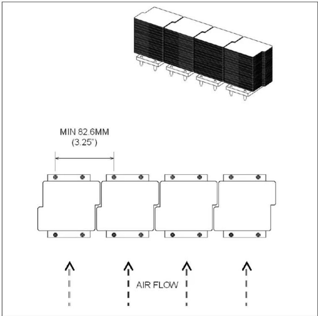
8.2.2 Boxed Processor Heatsink Weight
The boxed processor heatsink weight is approximately 530 grams. See Section 3 of this document for details on the processor weight.
8.2.3 Boxed Processor Retention Mechanism and Heatsink Supports
Baseboards and chassis's designed for use by system integrators should include holes that are in proper alignment with each other to support the boxed processor. See Figure 8-7 for example of processor pitch and layout.
Figure 8-1 illustrates the new retention solution. This is designed to extend air-cooling capability through the use of larger heatsinks with minimal airflow blockage and minimal bypass. These retention mechanisms can allow the use of much heavier heatsink masses compared to legacy
solution limitations by using a load path attached to the chassis pan. The hat spring on the under side of the baseboard provides the necessary compressive load for the thermal interface material. The baseboard is intended to be isolated such that the dynamic loads from the heatsink are transferred to the chassis pan via the heatsink screws and heatsink standoffs. This reduces the risk of package pullout and solder joint failures in a shock and vibe situation.
The assembly requires larger diameter holes to compensate for the CEK spring embosses. See Figure 8-2 and Figure 8-3 for processor mounting thorough holes.
8.3 Thermal Specifications
This section describes the cooling requirements of the heatsink solution utilized by the boxed processor.
8.3.1 Boxed Processor Cooling Requirements
The boxed processor will be cooled by forcing ducted chassis fan airflow through the passive heatsink solution. Meeting the processor's temperature specifications is a function of the thermal design of the entire system, and ultimately the responsibility of the system integrator. The processor temperature specification is found in Section 6 of this document. For the boxed processor passive heatsink to operate properly, chassis air movement devices are required. Necessary airflow and associated flow impedance is 29 cfm at 0.10" H _2 O.
In addition, the processor pitch should be 3.25 inches, or slightly more, when placed in side by side orientation. Figure 8-7 illustrates the side by side orientation and pitch. Note that the heatsinks are interleaved to reduce air bypass.
It is also recommended that the ambient air temperature outside of the chassis be kept at or below 35 ^ . The air passing directly over the processor heatsink should not be preheated by other system components (such as another processor), and should be kept at or below 40 ^ . Again, meeting the processor's temperature specification is the responsibility of the system integrator.
8.3.2 Boxed Processor Contents
The boxed processor will include the following items:
- Dual-Core Intel ^ Xeon ^ Processor 7000 Series
- Unattached passive heatsink with captive screws
• Thermal interface material (pre-attached) - Warranty/installation manual with Intel Inside logo
The other items required with this thermal solution should be shipped with either the chassis or the mainboard. They include:
- CEK spring (typically included with mainboard)
- Chassis standoffs
- System fans
9 Debug Tools Specifications
Please refer to the ITP700 Debug Port Design Guide, eXtended Debug Port: Debug Port Design Guide for Twin Castle Chipset Platforms, eXtended Debug Port: Debug Port Design Guide for MP Platforms, and the appropriate platform design guide for more detailed information regarding debug tools specifications.
9.1 Logic Analyzer Interface (LAI)
Intel is working with two logic analyzer vendors to provide logic analyzer interfaces (LAIs) for use in debugging Dual-Core Intel Xeon processor 7000 series systems. Tektronix and Agilent should be contacted to get specific information about their logic analyzer interfaces. The following information is general in nature. Specific information must be obtained from the logic analyzer vendor.
Due to the complexity of Dual-Core Intel Xeon processor 7000 series-based multiprocessor systems, the LAI is critical in providing the ability to probe and capture FSB signals. There are two sets of considerations to keep in mind when designing a Dual-Core Intel Xeon processor 7000 series-based system that can make use of an LAI: mechanical and electrical.
9.1.1 Mechanical Considerations
The LAI is installed between the processor socket and the processor. The LAI pins plug into the socket, while the processor pins plug into a socket on the LAI. Cabling that is part of the LAI egresses the system to allow an electrical connection between the processor and a logic analyzer. The maximum volume occupied by the LAI, known as the keepout volume, as well as the cable egress restrictions, should be obtained from the logic analyzer vendor. System designers must make sure that the keepout volume remains unobstructed inside the system. Note that it is possible that the keepout volume reserved for the LAI may differ from the space normally occupied by the Dual-Core Intel Xeon processor 7000 series heatsink. If this is the case, the logic analyzer vendor will provide a cooling solution as part of the LAI.
9.1.2 Electrical Considerations
The LAI will also affect the electrical performance of the FSB; therefore, it is critical to obtain electrical load models from each of the logic analyzer vendors to be able to run system level simulations to prove that their tool will work in the system. Contact the logic analyzer vendor for electrical specifications and load models for the LAI solution they provide.
- Dual-Core Intel® Xeon® Processor 7000 Series
- Contents
- Introduction....11
- Electrical Specifications....15
- Mechanical Specifications....33
- Pin Listing....41
- Signal Definitions....59
- Thermal Specifications....67
- Features....73
- Boxed Processor Specifications....97
- Debug Tools Specifications....107
- Figures
- Tables
- Revision History
- Terminology
- Reference Documents
- NOTES:
- State of Data
- Electrical Specifications
- Front Side Bus and GTLREF
- Front Side Bus Clock and Processor Clocking
- Front Side Bus Clock Select (BSEL[1:0])
- Phase Lock Loop (PLL) Power and Filter
- Voltage Identification (VID)
- Reserved, Unused, and TESTHI Pins
- Mixing Processors
- Front Side Bus Signal Groups
- GTL+ Asynchronous Signals and AGTL + Asynchronous Signals
- Test Access Port (TAP) Connection
- Absolute Maximum and Minimum Ratings
- Processor DC Specifications
- Flexible Motherboard (FMB) Guidelines
- Vcc Overshoot Specification
- Mechanical Specifications
- Package Mechanical Drawing
- Processor Component Keepout Zones
- Package Loading Specifications
- Package Handling Guidelines
- Package Insertion Specifications
- Processor Mass Specifications
- Processor Materials
- Processor Markings
- Processor Pin-Out Coordinates
- Dual-Core Intel Xeon Processor 7000 Series Pin Assignments
- Pin Listing by Pin Name
- Pin Listing by Pin Number
- Signal Definitions
- Signal Definitions
- Thermal Specifications
- Package Thermal Specifications
- Thermal Specifications
- Thermal Metrology
- Processor Thermal Features
- Thermal Monitor
- On-Demand Mode
- PROCHOT# Signal Pin
- FORCEPR# Signal Pin
- THERMTRIP# Signal Pin
- Tcontrol and Fan Speed Reduction
- Thermal Diode
- Power-On Configuration Options
- Clock Control and Low Power States
- Normal State
- HALT Power Down State
- Stop-Grant State
- HALT/Grant Snoop State
- Enhanced HALT Powerdown State
- Enhanced Intel SpeedStep ® Technology
- System Management Bus (SMBus) Interface
- Processor Information ROM (PIROM)
- Scratch EEPROM
- PIROM and Scratch EEPROM Supported SMBus Transactions
- SMBus Thermal Sensor
- Thermal Sensor Supported SMBus Transactions
- SMBus Thermal Sensor Registers
- Temperature Value Registers
- Thermal Limit Registers
- Status Registers
- Configuration Register
- Conversion Rate Register
- SMBus Thermal Sensor Alert Interrupt
- SMBus Device Addressing
- NOTE:
- Managing Data in the PIROM
- Header
- Processor Data
- Processor Core Data
- CPUID
- Front Side Bus Frequency
- Maximum Core Frequency
- Core Voltage
- T CASE Maximum
- Cache Data
- L2 Cache Size
- L3 Cache Size
- Cache Voltage
- Package Data
- Part Number Data
- Processor Part Number
- Processor Electronic Signature
- Feature Data
- Processor Core Feature Flags
- Processor Feature Flags
- Processor Thread and Core Information
- Additional Processor Feature Flags
- Thermal Adjustment Factors
- Other Data
- Checksums
- Boxed Processor Specifications
- Introduction
- Mechanical Specifications
- Boxed Processor Heatsink Dimensions
- Boxed Processor Heatsink Weight
- Boxed Processor Retention Mechanism and Heatsink Supports
- Thermal Specifications
- Boxed Processor Cooling Requirements
- Boxed Processor Contents
- Debug Tools Specifications
- Logic Analyzer Interface (LAI)
- Mechanical Considerations
- Electrical Considerations
Brand : INTEL
Model : Xeon 7041
Category : Processor