
SN74LS122N - Processor TEXAS INSTRUMENTS - Free user manual and instructions
Find the device manual for free SN74LS122N TEXAS INSTRUMENTS in PDF.


| Product Type | Integrated Circuit (IC) |
| Part Number | SN74LS122N |
| Brand | Texas Instruments |
| Category | Logic IC - Monostable Multivibrator |
| Logic Family | 74LS (Low-Power Schottky) |
| Number of Circuits | 2 (Dual) |
| Type | Retriggerable Monostable Multivibrator |
| Package Type | PDIP-16 (Plastic Dual-In-Line, 16 pins) |
| Supply Voltage (VCC) | 4.75 V to 5.25 V (Typical 5 V) |
| Operating Temperature Range | 0°C to 70°C |
| Output Type | Active Low and Active High |
| Trigger Types | Positive and Negative Edge Trigger |
| Output Pulse Width | Set by external R and C components |
| Maximum Propagation Delay | 30 ns (typical) |
| Power Dissipation | 45 mW (per package, typical) |
| Dimensions (Package) | 19.3 mm x 6.35 mm x 4.57 mm (nominal) |
| Weight | Approx. 1.3 g |
| RoHS Compliant | Yes |
| Main Functions | Pulse generation, timing, delay, and frequency division |
| Safety Precautions | Use within specified supply voltage; avoid ESD damage; observe max ratings |
| Cleaning and Maintenance | Not required for normal operation; keep away from moisture and debris |
| Spare Parts / Repairability | Non-repairable; replace with same part if defective |
| General Information | Dual retriggerable monostable multivibrator with reset capability |
Frequently Asked Questions - SN74LS122N TEXAS INSTRUMENTS
User questions about SN74LS122N TEXAS INSTRUMENTS
0 question about this device. Answer the ones you know or ask your own.
Ask a new question about this device
Download the instructions for your Processor in PDF format for free! Find your manual SN74LS122N - TEXAS INSTRUMENTS and take your electronic device back in hand. On this page are published all the documents necessary for the use of your device. SN74LS122N by TEXAS INSTRUMENTS.
USER MANUAL SN74LS122N TEXAS INSTRUMENTS
● D-C Triggered from Active-High or Active-Low Gated Logic Inputs
● Retriggerable for Very Long Output Pulses, Up to 100% Duty Cycle
● Overriding Clear Terminates Output Pulse
- '122 and 'LS122 Have Internal Timing Resistors
description
These d-c triggered multivibrators feature output pulse-duration control by three methods. The basic pulse time is programmed by selection of external resistance and capacitance values (see typical application data). The '122 and 'LS122 have internal timing resistors that allow the circuits to be used with only an external capacitor, if so desired. Once triggered, the basic pulse duration may be extended by retriggering the gated low-level-active (A) or high-level-active (B) inputs, or be reduced by use of the overriding clear. Figure 1 illustrates pulse control by retriggering and early clear.
The 'LS122 and 'LS123 are provided enough Schmitt hysteresis to ensure jitter-free triggering from the B input with transition rates as slow as 0.1 millivolt per nanosecond.
The R_int in nominall 10 kΩ for '122 and 'LS122.
SN54122, SN54LS122 ... J OR W PACKAGE
SN74122 ... N PACKAGE
SN74LS122 ... D OR N PACKAGE
(TOP VIEW) (SEE NOTES 1 THRU 4)
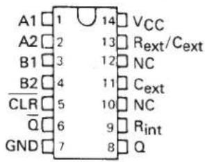
NOTES: 1. An external timing capacitor may be connected between C_ext and R_ext / C_ext (positive).
-
To use the internal timing resistor of '122 or 'LS122, connect R_int to V_CC .
-
For improved pulse duration accuracy and repeatability, connect an external resistor between R_ext/C_ext and V_CC with R_int open-circuited.
-
To obtain variable pulse durations, connect an external variable resistance between R_int or R_ext/C_ext and V_CC .
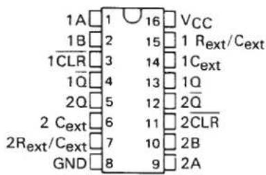
SN54123, SN54130, SN54LS123 ... J OR W PACKAGE
SN74123, SN74130 ... N PACKAGE
SN74LS123 ... D OR N PACKAGE
(TOP VIEW) (SEE NOTES 1 THRU 4)
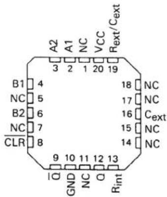
SN54LS122 ... FK PACKAGE
(TOP VIEW) (SEE NOTES 1 THRU 4)
SN54LS123...FK PACKAGE
(TOP VIEW) (SEE NOTES 1 THRU 4)
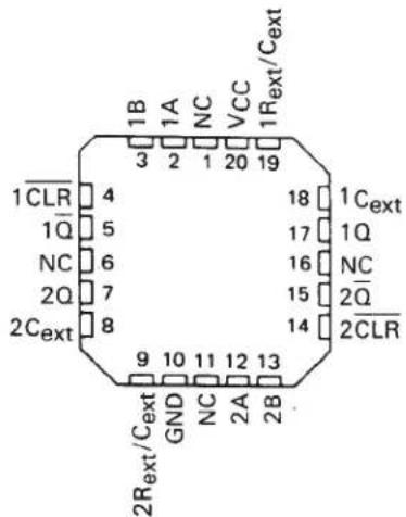
NC - No internal connection
description (continued)
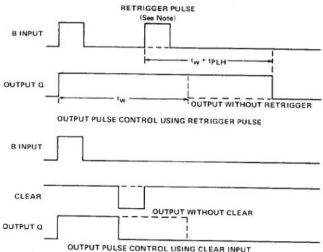
NOTE: Retrigger pulses starting before 0.22 C _ext (in picofrads) nanoseconds after the initial trigger pulse will be ignored and the output duration will remain unchanged.
FIGURE 1-TYPICAL INPUT/OUTPUT PULSES
'122, 'LS122
FUNCTION TABLE
| INPUTS | OUTPUTS | |||||
| CLEAR | A1 | A2 | B1 | B2 | Q | |
| L | X | X | X | X | L | H |
| X | H | H | X | X | L^† | H^† |
| X | X | X | L | X | L^† | H^† |
| X | X | X | X | L | L^† | H^† |
| H | L | X | ↑ | H | ||
| H | L | X | H | ↑ | ||
| H | X | L | ↑ | H | ||
| H | X | L | H | ↑ | ||
| H | H | ↓ | H | H | ||
| H | ↓ | ↓ | H | H | ||
| H | ↓ | H | H | H | ||
| ↑ | L | X | H | H | ||
| ↑ | X | L | H | H | ||
'123, '130, 'LS123 FUNCTION TABLE
| INPUTS | OUTPUTS | |||
| CLEAR | A | B | Q | |
| L | X | X | L | H |
| X | H | X | L^† | H^† |
| X | X | L | L^† | H^† |
| H | L | ↑ | ∩ | ∪ |
| H | ↓ | H | ∩ | ∪ |
| ↑ | L | H | ∩ | ∪ |
See explanation of function tables on page
† These lines of the functional tables assume that the indicated steady-state conditions at the A and B inputs have been set up long enough to complete any pulse started before the set up.
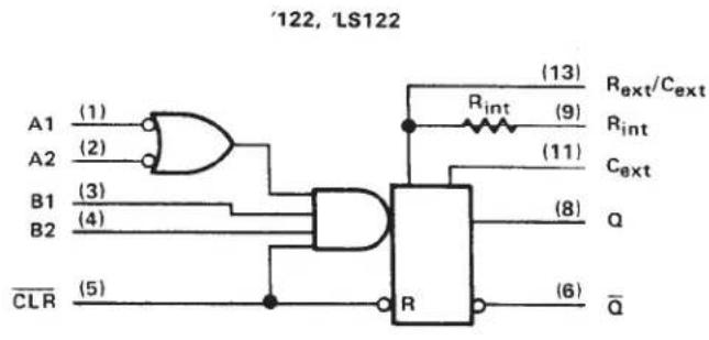
logic diagram (positive logic)
flowchart
graph TD
    A["1"] --> B["OR"]
    C["2"] --> B
    D["3"] --> E["AND"]
    F["4"] --> E
    G["5"] --> H["R"]
    I["6"] --> H
    J["7"] --> H
    K["8"] --> H
    L["9"] --> M["Rint"]
    N["10"] --> M
    O["11"] --> P["Cext"]
    Q["12"] --> P
    R["13"] --> S["Rext/Cext"]
    T["Q̅"] --> U["Q̅"]
    V["CLR"] --> W["Ground"]
    style A fill:#f9f,stroke:#333
    style C fill:#f9f,stroke:#333
    style D fill:#f9f,stroke:#333
    style B fill:#ccf,stroke:#333
    style E fill:#ccf,stroke:#333
    style H fill:#ccf,stroke:#333
    style M fill:#ccf,stroke:#333
    style P fill:#ccf,stroke:#333
    style Q fill:#ccf,stroke:#333
    style U fill:#ccf,stroke:#333
    style R fill:#ccf,stroke:#333
    style S fill:#ccf,stroke:#333
    style T fill:#ccf,stroke:#333
    style Q fill:#ccf,stroke:#333
    style U fill:#ccf,stroke:#333
logic symbol ^†
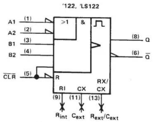
R_int is nominally 10 kΩ for '122 and 'LS122
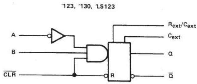
logic diagram (positive logic) (each multivibrator)
flowchart
graph TD
    A["A"] --> AND1["NOT"]
    B["B"] --> AND1
    AND1 --> D["AND"]
    CLR["CLR"] --> D
    D --> R["R"]
    R --> Rext["C_ext"]
    Rext --> Cext["C_ext"]
    Rext --> Q["a"]
    Rext --> Qbar["Q̅"]
    style A fill:#f9f,stroke:#333
    style B fill:#f9f,stroke:#333
    style CLR fill:#f9f,stroke:#333
    style D fill:#ccf,stroke:#333
    style R fill:#cfc,stroke:#333
    style Rext fill:#fcc,stroke:#333
    style Cext fill:#fcc,stroke:#333
    style Q fill:#fff,stroke:#333
    style Qbar fill:#fff,stroke:#333
Pin numbers shown are for D, J, N, and W packages.
logic symbol ^†
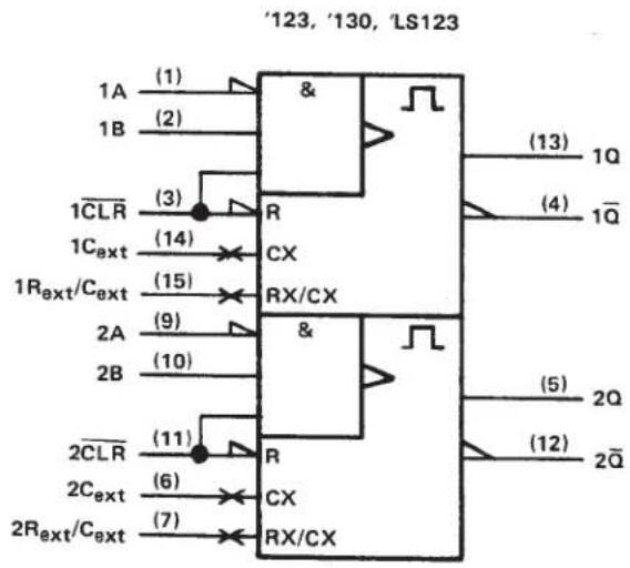
flowchart
graph TD
    A["1A (1)"] --> B["&"]
    C["1B (2)"] --> B
    D["1CLR (3)"] --> E["R"]
    F["1C_ext (4)"] --> G["CX"]
    H["1R_ext/C_ext (5)"] --> I["RX/CX"]
    J["2A (9)"] --> K["&"]
    L["2B (10)"] --> K
    M["2CLR (11)"] --> N["R"]
    O["2C_ext (6)"] --> P["CX"]
    Q["2R_ext/C_ext (7)"] --> R["RX/CX"]
    B --> S["(13) 1Q"]
    G --> T["(4) 1Q̅"]
    K --> U["(5) 2Q"]
    R --> V["(12) 2Q̅"]
    style B fill:#f9f,stroke:#333
    style K fill:#f9f,stroke:#333
    style U fill:#f9f,stroke:#333
    style V fill:#f9f,stroke:#333
^† These symbols are in accordance with ANSI/IEEE Std 91-1984 and IEC Publication 617-12.
schematics of inputs and outputs
'122, '123, '130 CIRCUITS
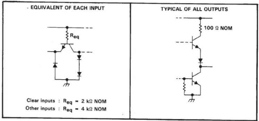
'LS122, 'LS123 CIRCUITS
| EQUIVALENT OF EACH INPUT 17 kΩ NOM | TYPICAL OF ALL OUTPUTS 120 Ω NOM |
absolute maximum ratings over operating free-air temperature range (unless otherwise noted)
Supply voltage, VCC (see Note 1) 7 V
Input voltage: '122, '123, '130 5.5V
'LS122, 'LS123 7 V
Operating free-air temperature range: SN54' -55°C to 125°C
SN74' 0°C to 70°C
Storage temperature range -65°C to 150°C
NOTE 1: Voltage values are with respect to network ground terminal.
recommended operating conditions
| SN54' | SN74' | UNIT | |||||
| MIN | NOM | MAX | MIN | NOM | MAX | ||
| Supply voltage, V_CC | 4.5 | 5 | 5.5 | 4.75 | 5 | 5.25 | V |
| High-level output current, I_OH | -800 | -800 | A | ||||
| Low-level output current, I_OL | 16 | 16 | mA | ||||
| Pulse duration, t_w | 40 | 40 | ns | ||||
| External timing resistance, R_ext | 5 | 25 | 5 | 50 | k | ||
| External capacitance, C_ext | No restriction | No restriction | |||||
| Wiring capacitance at R_ext/C_ext terminal | 50 | 50 | pF | ||||
| Operating free-air temperature, T_A | -55 | 125 | 0 | 70 | °C | ||
electrical characteristics over recommended free-air operating temperature range (unless otherwise noted)
| PARAMETER | TEST CONDITIONS† | '122 | '123, '130 | UNIT | ||||||
| MIN | TYP‡ | MAX | MIN | TYP‡ | MAX | |||||
| VIH | High-level input voltage | 2 | 2 | V | ||||||
| VIL | Low-level input voltage | 0.8 | 0.8 | V | ||||||
| VIK | Input clamp voltage | VCC=MIN, I1=-12 mA | -1.5 | -1.5 | V | |||||
| VOH | High-level output voltage | VCC=MIN, IOH=-800 μA, See Note 5 | 2.4 | 3.4 | 2.4 | 3.4 | V | |||
| VOL | Low-level output voltage | VCC=MIN, IOL=16 mA, See Note 5 | 0.2 | 0.4 | 0.2 | 0.4 | V | |||
| II | Input current at maximum input voltage | VCC=MAX, VI=5.5 V | 1 | 1 | mA | |||||
| IIH | High-level input current | Data inputs | VCC=MAX, VI=2.4 V | 40 | 40 | μA | ||||
| Clear input | 80 | 80 | ||||||||
| IIL | Low-level input current | Data inputs | VCC=MAX, VI=0.4 V | -1.6 | -1.6 | mA | ||||
| Clear input | -3.2 | -3.2 | ||||||||
| IOS | Short-circuit output current§ | VCC=MAX, See Note 5 | -10 | -40 | -10 | -40 | mA | |||
| ICC | Supply current (quiescent or triggered) | VCC=MAX, See Notes 6 and 7 | 23 | 36 | 46 | 66 | mA | |||
^ For conditions shown as MIN or MAX, use the appropriate value specified under recommended operating conditions.
^+ All typical values are at V_CC = 5 V , T_A = 25^ .
^9 Not more than one output should be shorted at a time.
NOTES: 5. Ground C_ext to measure V_OH at Q, V_OL at , or I_OS at Q. C_ext is open to measure V_OH at , V_OL at Q, or I_OS at .
-
Quiescent I_CC is measured (after clearing) with 4.5 V applied to all clear and A inputs, B inputs grounded, all outputs open and R_ext = 25 k . R_int of '122 is open.
-
I_CC is measured in the triggered state with 2.4 V applied to all clear and B inputs, A inputs grounded, all outputs open, C_ext = 0.02 F , and R_ext = 25k . R_int of '122 is open.
switching characteristics, VCC = 5 V, TA = 25°C, see note 8
| PARAMETER¶ | FROM(INPUT) | TO(OUTPUT) | TEST CONDITIONS | '122, '130 | '123 | UNIT | ||||
| MIN | TYP | MAX | MIN | TYP | MAX | |||||
| tPLH | A | Q | C_ext=0, R_ext=5k , C_L=15pF, R_L=400 | 22 | 33 | 22 | 33 | ns | ||
| B | 19 | 28 | 19 | 28 | ||||||
| tPHL | A | Q | 30 | 40 | 30 | 40 | ns | |||
| B | 27 | 36 | 27 | 36 | ||||||
| tPHL | Clear | Q | 18 | 27 | 18 | 27 | ns | |||
| tPLH | Q | 30 | 40 | 30 | 40 | |||||
| twQ (min) | A or B | Q | 45 | 65 | 45 | 76 | ns | |||
| twQ | A or B | Q | C_ext=1000pF, R_ext=10k , C_L=15pF, R_L=400 | 3.08 | 3.42 | 3.76 | 2.76 | 3.03 | 3.37 | μs |
^1 tPLH = propagation delay time, low-to-high-level output
t_PHL = propagation delay time, high-to-low-level output
t_wQ = duration of pulse at output Q.
NOTE 8: Load circuits and voltage waveforms are shown in Section 1.
SDLS043 - DECEMBER 1983 - REVISED MARCH 1988
recommended operating conditions
| SN54LS' | SN74LS' | UNIT | |||||
| MIN | NOM | MAX | MIN | NOM | MAX | ||
| Supply voltage, VCC | 4.5 | 5 | 5.5 | 4.75 | 5 | 5.25 | V |
| High-level output current, IOH | -400 | -400 | μA | ||||
| Low-level output current, IOL | 4 | 8 | mA | ||||
| Pulse duration, tw | 40 | 40 | ns | ||||
| External timing resistance, Rext | 5 | 180 | 5 | 260 | kΩ | ||
| External capacitance, Cext | No restriction | No restriction | |||||
| Wiring capacitance at Rext/Cext terminal | 50 | 50 | pF | ||||
| Operating free-air temperature, TA | -55 | 125 | 0 | 70 | °C | ||
electrical characteristics over recommended operating free-air temperature range (unless otherwise noted)
| PARAMETER | TEST CONDITIONS† | SN54LS' | SN74LS' | UNIT | |||||||
| MIN | TYP‡ | MAX | MIN | TYP‡ | MAX | ||||||
| V_IH | High-level input voltage | 2 | 2 | V | |||||||
| V_IL | Low-level input voltage | 0.7 | 0.8 | V | |||||||
| V_IK | Input clamp voltage | V_CC=MIN, I_I=-18 mA | -1.5 | -1.5 | V | ||||||
| V_OH | High-level output voltage | V_CC=MIN, V_IL=V_ILmax | V_IH=2 V, I_OH=-400 μA | 2.5 | 3.5 | 2.7 | 3.5 | V | |||
| V_OL | Low-level output voltage | V_CC=MIN, V_IL=V_ILmax | V_IH=2 V, | I_OL=4 mA | 0.25 | 0.4 | 0.25 | 0.4 | V | ||
| I_OL=8 mA | 0.35 | 0.5 | |||||||||
| I_I | Input current at maximum input voltage | V_CC=MAX, V_I=7 V | 0.1 | 0.1 | mA | ||||||
| I_IH | High-level input current | V_CC=MAX, V_I=2.7 V | 20 | 20 | μA | ||||||
| I_IL | Low-level input current | V_CC=MAX, V_I=0.4 V | -0.4 | -0.4 | mA | ||||||
| IOS | Short-circuit output currents§ | V_CC=MAX | -20 | -100 | -20 | -100 | mA | ||||
| I_CC | Supply current (quiescent or triggered) | V_CC=MAX, See Note 13 | 'LS122 | 6 | 11 | 6 | 11 | mA | |||
| 'LS123 | 12 | 20 | 12 | 20 | |||||||
^ For conditions shown as MIN or MAX, use the appropriate value specified under recommended operating conditions.
^ All typical values are at V_CC = 5 V , T_A = 25^ .
^§ Not more than one output should be shorted at a time and duration of the short-circuit should not exceed one second.
NOTES: 12. To measure V_OH at Q, V_OL at Q, or I_OS at Q, ground R_ext/C_ext , apply 2 V to B and clear, and pulse A from 2 V to 0 V.
13. With all outputs open and 4.5 V applied to all data and clear inputs. Icc is measured after a momentary ground, then 4.5 V, is applied to A or B inputs.
switching characteristics, V_CC = 5 V, T_A = 25^ (see note 8)
| PARAMETER1 | FROM(INPUT) | TO(OUTPUT) | TEST CONDITIONS | MIN | TYP | MAX | UNIT |
| tPLH | A | Q | C_ext = 0, R_ext = 5 k, C_L = 15 pF, R_L = 2 k | 23 | 33 | ns | |
| B | 23 | 44 | |||||
| tPHL | A | Q | 32 | 45 | ns | ||
| B | 34 | 56 | |||||
| tPHL | Clear | Q | 20 | 27 | ns | ||
| tPLH | Q | 28 | 45 | ||||
| twQ (min) | A or B | Q | 116 | 200 | ns | ||
| twQ | A or B | Q | C_ext = 1000 pF, R_ext = 10 k, C_L = 15 pF, R_L = 2 k | 4 | 4.5 | 5 | μs |
t_PLH = propagation delay time, low-to-high-level output
t_PHL = propagation delay time, high-to-low-level output
t_wQ = duration of pulse at output Q.
NOTE 8: Load circuits and voltage waveforms are shown in Section 1.
TYPICAL APPLICATION DATA FOR '122, '123, '130
For pulse durations when C_ext ≤ 1000 pF, see Figure 4.
The output pulse duration is primarily a function of the external capacitor and resistor. For C_ext > 1000 pF, the output pulse duration ( t_w ) is defined as:
$$ t _ {W} = K \cdot R _ {T} \cdot C _ {\text { ext }} \left(1 + \frac {0 . 7}{R _ {T}}\right) $$
where
K is 0.32 for '122, 0.28 for '123 and '130
R_T is in kΩ (internal or external timing resistance.)
C_ext is in pF
t_w is in ns
To prevent reverse voltage across C_ext , it is recommended that the method shown in Figure 2 be employed when using electrolytic capacitors and in applications utilizing the clear function. In all applications using the diode, the pulse duration is:
$$ t _ {W} = K _ {D} \cdot R _ {T} \cdot C _ {\text { ext }} \left(1 + \frac {0 . 7}{R _ {T}}\right) $$
K_D is 0.28 for '122, 0.25 for '123 and '130
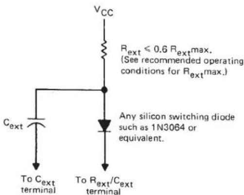
TIMING COMPONENT CONNECTIONS WHEN
C_ext > 1000 pF AND CLEAR IS USED
FIGURE 2
Applications requiring more precise pulse durations (up to 28 seconds) and not requiring the clear feature can best be satisfied with the '121.
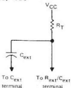
TIMING COMPONENT CONNECTIONS FIGURE 3
TYPICAL OUTPUT PULSE DURATION
VS
EXTERNAL TIMING CAPACITANCE
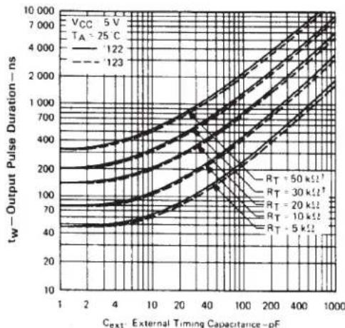
line
| CeAT: External Timing Capacitance - pF | VCC 5 V | TA = 25 C | TA = 122 | TA = 123 | | -------------------------------------- | ------- | --------- | -------- | -------- | | 1 | ~350 | ~350 | ~350 | ~350 | | 2 | ~400 | ~400 | ~400 | ~400 | | 4 | ~500 | ~500 | ~500 | ~500 | | 10 | ~700 | ~700 | ~700 | ~700 | | 20 | ~1000 | ~1000 | ~1000 | ~1000 | | 40 | ~1500 | ~1500 | ~1500 | ~1500 | | 100 | ~2500 | ~2500 | ~2500 | ~2500 | | 200 | ~4000 | ~4000 | ~4000 | ~4000 | | 400 | ~6000 | ~6000 | ~6000 | ~6000 | | 1000 | ~8000 | ~8000 | ~8000 | ~8000 |FIGURE 4
^† These values of resistance exceed the maximum recommended for use over the full temperature range of the SN54' circuits.
TYPICAL APPLICATION DATA FOR 'LS122, 'LS123
The basic output pulse duration is essentially determined by the values of external capacitance and timing resistance. For pulse durations when C_ext ≤ 1000 pF, use Figure 6, or use Figure 7 where the pulse duration may be defined as:
$$ t _ {W} = K \cdot R _ {T} \cdot C _ {\text { ext }} $$
When C_ext ≥ 1 F , the output pulse width is defined as:
$$ t _ {w} = 0. 3 3 \cdot R _ {T} \cdot C _ {\text { ext }} $$
For the above two equations, as applicable;
K is multiplier factor, see Figure 7
R_T is in kΩ (internal or external timing resistance)
C_ext is in pF
t_w is in ns
For maximum noise immunity, system ground should be applied to the C_ext node, even though the C_ext node is already tied to the ground lead internally. Due to the timing scheme used by the 'LS122 and 'LS123, a switching diode is not required to prevent reverse biasing when using electrolytic capacitors.
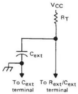
TIMING COMPONENT CONNECTIONS FIGURE 5
'LS122, 'LS123
TYPICAL OUTPUT PULSE DURATION
VS
EXTERNAL TIMING CAPACITANCE
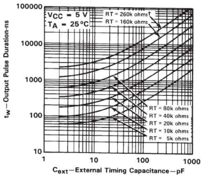
line
| C_ext - External Timing Capacitance - pF | t_w - Output Pulse Duration-ns (RT = 260k ohms) | t_w - Output Pulse Duration-ns (RT = 160k ohms) | t_w - Output Pulse Duration-ns (RT = 80k ohms) | t_w - Output Pulse Duration-ns (RT = 40k ohms) | t_w - Output Pulse Duration-ns (RT = 20k ohms) | t_w - Output Pulse Duration-ns (RT = 10k ohms) | t_w - Output Pulse Duration-ns (RT = 5k ohms) | | ---------------------------------------- | ----------------------------------------------- | ----------------------------------------------- | ----------------------------------------------- | ----------------------------------------------- | ----------------------------------------------- | ----------------------------------------------- | ----------------------------------------------- | | 1 | ~100 | ~100 | ~100 | ~100 | ~100 | ~100 | ~100 | | 10 | ~1000 | ~1000 | ~1000 | ~1000 | ~1000 | ~1000 | ~1000 | | 100 | ~10000 | ~10000 | ~10000 | ~10000 | ~10000 | ~10000 | ~10000 | | 1000 | ~10000 | ~10000 | ~10000 | ~10000 | ~10000 | ~10000 | ~10000 |^ This value of resistance exceeds the maximum recommended for use over the full temperature range of the SN54LS circuits.
FIGURE 6
TYPICAL APPLICATION DATA FOR 'LS122, 'LS123†
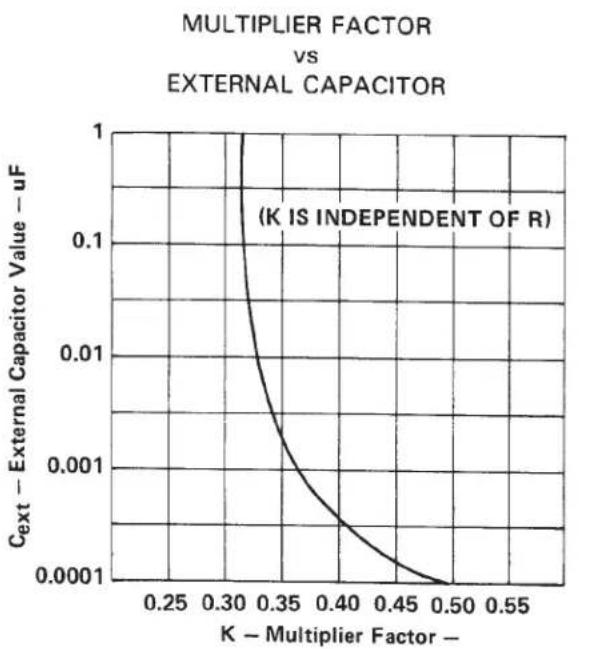
line
| K - Multiplier Factor | C_ext - External Capacitor Value - uF | | --------------------- | -------------------------------------- | | 0.30 | 1.0 | | 0.35 | 0.1 | | 0.40 | 0.01 | | 0.45 | 0.001 | | 0.50 | 0.0001 | | 0.55 | 0.0001 |FIGURE 7
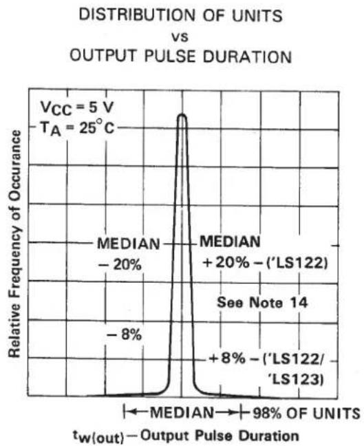
line
| Metric | Value | |--------|-------| | VCC | 5 V | | TA | 25°C | | Median | -20% | | Mean | +20% | | LS122 | ('LS122) | | Mean | +8% | | LS123 | ('LS122/'LS123) | | Median → 98% of Units tW(out)→ Output Pulse Duration See Note 14FIGURE 8
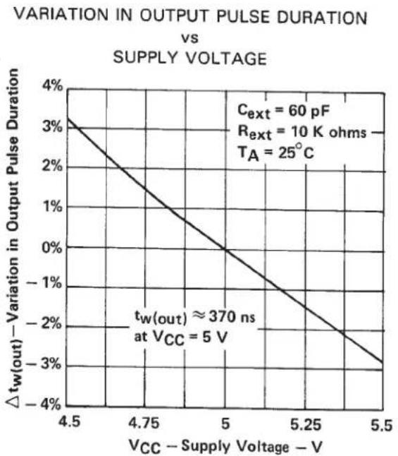
line
| VCC - Supply Voltage - V | Δtw(out) - Variation in Output Pulse Duration | | ------------------------ | --------------------------------------------- | | 4.5 | 3% | | 5.0 | 0% | | 5.5 | -3% |FIGURE 9
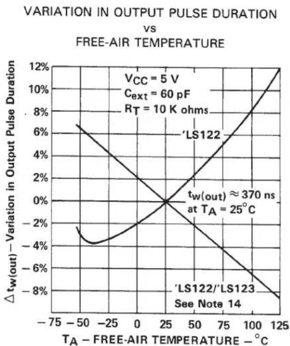
line
| TA - Free-Air Temperature (°C) | Δtw(out) - Variation in Output Pulse Duration | | ------------------------------ | --------------------------------------------- | | -50 | -4% | | 0 | 0% | | 25 | 0% | | 50 | 2% | | 75 | 4% | | 100 | 6% | | 125 | 8% |FIGURE 10
NOTE 14: For the 'LS122, the internal timing resistor, R_int was used. For the 'LS122/123, an external timing resistor was used for R_T . ^ Data for temperatures below 0°C and above 70°C and for supply voltages below 4.75 V and above 5.25 V are applicable for SN54LS122 and SN54LS123 only.
PACKAGING INFORMATION
| Orderable Device Status(1) | Package Type | Package Drawing | Pins | Package Qty | Eco Plan(2) | Lead finish/ Ball material(6) | MSL Peak Temp(3) | Op Temp (°C) | Device Marking(4/5) | Samples |
| 5962-7603901VEA ACTIVE CDIP J 16 1 Non-RoHS | & Green | SNPB N / A for Pkg Type -55 to 125 5962-7603901VE | ASNV54LS123J | Samples | ||||||
| 5962-7603901VFA ACTIVE CFP W 16 1 Non-RoHS | & Green | SNPB N / A for Pkg Type -55 to 125 5962-7603901VF | ASNV54LS123W | Samples | ||||||
| 7603901EA ACTIVE CDIP J 16 1 Non-RoHS | & Green | SNPB N / A for Pkg Type -55 to 125 7603901EA | SNJ54LS123J | Samples | ||||||
| 7603901FA ACTIVE CFP W 16 1 Non-RoHS | & Green | SNPB N / A for Pkg Type -55 to 125 7603901FA | SNJ54LS123W | Samples | ||||||
| JM38510/01203BEA ACTIVE CDIP J 16 1 Non-RoHS | & Green | SNPB N / A for Pkg Type -55 to 125 JM38510/ | 01203BEA | Samples | ||||||
| JM38510/31401B2A ACTIVE LCCC FK 20 1 Non-RoHS | & Green | SNPB N / A for Pkg Type -55 to 125 JM38510/ | 31401B2A | Samples | ||||||
| JM38510/31401BEA ACTIVE CDIP J 16 1 Non-RoHS | & Green | SNPB N / A for Pkg Type -55 to 125 JM38510/ | 31401BEA | Samples | ||||||
| JM38510/31401BFA ACTIVE CFP W 16 1 Non-RoHS | & Green | SNPB N / A for Pkg Type -55 to 125 JM38510/ | 31401BFA | Samples | ||||||
| M38510/01203BEA | ACTIVE CDIP J 16 1 Non-RoHS | & Green | SNPB N / A for Pkg Type -55 to 125 JM38510/ | 01203BEA | Samples | |||||
| M38510/31401B2A | ACTIVE LCCC FK 20 1 Non-RoHS | & Green | SNPB N / A for Pkg Type -55 to 125 JM38510/ | 31401B2A | Samples | |||||
| M38510/31401BEA | ACTIVE CDIP J 16 1 Non-RoHS | & Green | SNPB N / A for Pkg Type -55 to 125 JM38510/ | 31401BEA | Samples | |||||
| M38510/31401BFA | ACTIVE CFP W 16 1 Non-RoHS | & Green | SNPB N / A for Pkg Type -55 to 125 JM38510/ | 31401BFA | Samples | |||||
| SN54123J | ACTIVE CDIP J 16 1 Non-RoHS | & Green | SNPB N / A for Pkg Type -55 to 125 SN54123J | Samples | ||||||
| SN54LS123J | ACTIVE CDIP J 16 1 Non-RoHS | & Green | SNPB N / A for Pkg Type -55 to 125 SN54LS123J | Samples | ||||||
| SN74123N | ACTIVE PDIP N | 16 | 25 | RoHS & Green | NIPDAU | N / A for Pkg Type | 0 to 70 | SN74123N | Samples | |
| SN74LS122D | ACTIVE SOIC D | 14 | 50 | RoHS & Green | NIPDAU | Level-1-260C-UNLIM | 0 to 70 | LS122 | Samples | |
Addendum-Page 1
| Orderable Device Status(1) | Package Type | Package Drawing | Pins | Package Qty | Eco Plan(2) | Lead finish/ Ball material(6) | MSL Peak Temp(3) | Op Temp (°C) | Device Marking(4-5) | Samples | |
| SN74LS122DR ACTIVE SOIC D 14 2500 RoHS & Green NIPDAU Level-1-260C-UNLIM 0 to 70 LS122 | Samples | ||||||||||
| SN74LS122DRE4 ACTIVE SOIC D 14 2500 RoHS & Green NIPDAU Level-1-260C-UNLIM 0 to 70 LS122 | Samples | ||||||||||
| SN74LS122N | ACTIVE | PDIP | N | 14 | 25 | RoHS & Green | NIPDAU | N / A for Pkg Type | 0 to 70 | SN74LS122N | Samples |
| SN74LS122NE4 | ACTIVE | PDIP | N | 14 | 25 | RoHS & Green | NIPDAU | N / A for Pkg Type | 0 to 70 | SN74LS122N | Samples |
| SN74LS122NSR | ACTIVE | SO | NS | 14 | 2000 | RoHS & Green | NIPDAU | Level-1-260C-UNLIM | 0 to 70 | 74LS122 | Samples |
| SN74LS123D ACTIVE SOIC D 16 40 RoHS & Green NIPDAU Level-1-260C-UNLIM 0 to 70 LS123 | Samples | ||||||||||
| SN74LS123DBR | ACTIVE | SSOP | DB | 16 | 2000 | RoHS & Green | NIPDAU | Level-1-260C-UNLIM | LS123 | Samples | |
| SN74LS123DE4 | ACTIVE | SOIC | D | 16 | 40 | RoHS & Green | NIPDAU | Level-1-260C-UNLIM | 0 to 70 | LS123 | Samples |
| SN74LS123DG4 | ACTIVE | SOIC | D | 16 | 40 | RoHS & Green | NIPDAU | Level-1-260C-UNLIM | 0 to 70 | LS123 | Samples |
| SN74LS123DR ACTIVE SOIC D 16 2500 RoHS & Green NIPDAU Level-1-260C-UNLIM 0 to 70 LS123 | Samples | ||||||||||
| SN74LS123DRE4 ACTIVE SOIC D 16 2500 RoHS & Green NIPDAU Level-1-260C-UNLIM 0 to 70 LS123 | Samples | ||||||||||
| SN74LS123DRG4 | ACTIVE SOIC D 16 2500 RoHS & Green NIPDAU Level-1-260C-UNLIM 0 to 70 LS123 | Samples | |||||||||
| SN74LS123N | ACTIVE | PDIP | N | 16 | 25 | RoHS & Green | NIPDAU | N / A for Pkg Type | 0 to 70 | SN74LS123N | Samples |
| SN74LS123NE4 | ACTIVE | PDIP | N | 16 | 25 | RoHS & Green | NIPDAU | N / A for Pkg Type | 0 to 70 | SN74LS123N | Samples |
| SN74LS123NSR | ACTIVE | SO | NS | 16 | 2000 | RoHS & Green | NIPDAU | Level-1-260C-UNLIM | 0 to 70 | 74LS123 | Samples |
| SN74LS123NSRG4 | ACTIVE | SO | NS | 16 | 2000 | RoHS & Green | NIPDAU | Level-1-260C-UNLIM | 0 to 70 | 74LS123 | Samples |
| SNJ54123J | ACTIVE | CDIP | J | 16 | 1 | Non-RoHS & Green | SNPB N / A for Pkg Type | -55 to 125 | SNJ54123J | Samples | |
| SNJ54123W | ACTIVE | CFP | W | 16 | 1 | Non-RoHS & Green | SNPB N / A for Pkg Type | -55 to 125 | SNJ54123W | Samples | |
| SNJ54LS123FK | ACTIVE | LCCC | FK | 20 | 1 | Non-RoHS & Green | SNPB N / A for Pkg Type | -55 to 125 | SNJ54LS123FK | Samples | |
| SNJ54LS123J | ACTIVE | CDIP | J | 16 | 1 | Non-RoHS & Green | SNPB N / A for Pkg Type | -55 to 125 | 7603901EASNJ54LS123J | Samples | |
| Orderable Device Status(1) | Package Type Package Drawing | Pins Package Qty | Eco Plan(2) | Lead finish/ Ball material(6) | MSL Peak Temp(3) | Op Temp (°C) | Device Marking(4-5) | Samples |
| SNJ54LS123W ACTIVE CFP W 16 1 Non-RoHS | & Green | SNPB N / A for Pkg Type -55 to 125 7603901FA | SNJ54LS123W | Samples | ||||
(1) The marketing status values are defined as follows:
ACTIVE: Product device recommended for new designs.
LIFEBUY: TI has announced that the device will be discontinued, and a lifetime-buy period is in effect.
NRND: Not recommended for new designs. Device is in production to support existing customers, but TI does not recommend using this part in a new design.
PREVIEW: Device has been announced but is not in production. Samples may or may not be available.
OBSOLETE: TI has discontinued the production of the device.
(2) RoHS: TI defines "RoHS" to mean semiconductor products that are compliant with the current EU RoHS requirements for all 10 RoHS substances, including the requirement that RoHS substance do not exceed 0.1% by weight in homogeneous materials. Where designed to be soldered at high temperatures, "RoHS" products are suitable for use in specified lead-free processes. TI may reference these types of products as "Pb-Free".
RoHS Exempt: TI defines "RoHS Exempt" to mean products that contain lead but are compliant with EU RoHS pursuant to a specific EU RoHS exemption.
Green: TI defines "Green" to mean the content of Chlorine (Cl) and Bromine (Br) based flame retardants meet JS709B low halogen requirements of <=1000ppm threshold. Antimony trioxide based flame retardants must also meet the <=1000ppm threshold requirement.
(3) MSL, Peak Temp. - The Moisture Sensitivity Level rating according to the JEDEC industry standard classifications, and peak solder temperature.
(4) There may be additional marking, which relates to the logo, the lot trace code information, or the environmental category on the device.
(5) Multiple Device Markings will be inside parentheses. Only one Device Marking contained in parentheses and separated by a "-" will appear on a device. If a line is indented then it is a continuation of the previous line and the two combined represent the entire Device Marking for that device.
(6) Lead finish/Ball material - Orderable Devices may have multiple material finish options. Finish options are separated by a vertical ruled line. Lead finish/Ball material values may wrap to two lines if the finish value exceeds the maximum column width.
Important Information and Disclaimer: The information provided on this page represents TI's knowledge and belief as of the date that it is provided. TI bases its knowledge and belief on information provided by third parties, and makes no representation or warranty as to the accuracy of such information. Efforts are underway to better integrate information from third parties. TI has taken and continues to take reasonable steps to provide representative and accurate information but may not have conducted destructive testing or chemical analysis on incoming materials and chemicals. TI and TI suppliers consider certain information to be proprietary, and thus CAS numbers and other limited information may not be available for release.
In no event shall TI's liability arising out of such information exceed the total purchase price of the TI part(s) at issue in this document sold by TI to Customer on an annual basis.
OTHER QUALIFIED VERSIONS OF SN54123, SN54LS123, SN54LS123-SP, SN74123, SN74LS123 :

TEXAS
INSTRUMENTS
www.ti.com
PACKAGE OPTION ADDENDUM
9-Feb-2022
• Catalog : SN74123, SN74LS123, SN54LS123
• Military : SN54123, SN54LS123
• Space : SN54LS123 SP
NOTE: Qualified Version Definitions:
• Catalog - TI's standard catalog product
• Military - QML certified for Military and Defense Applications
• Space - Radiation tolerant, ceramic packaging and qualified for use in Space-based application
TAPE AND REEL INFORMATION
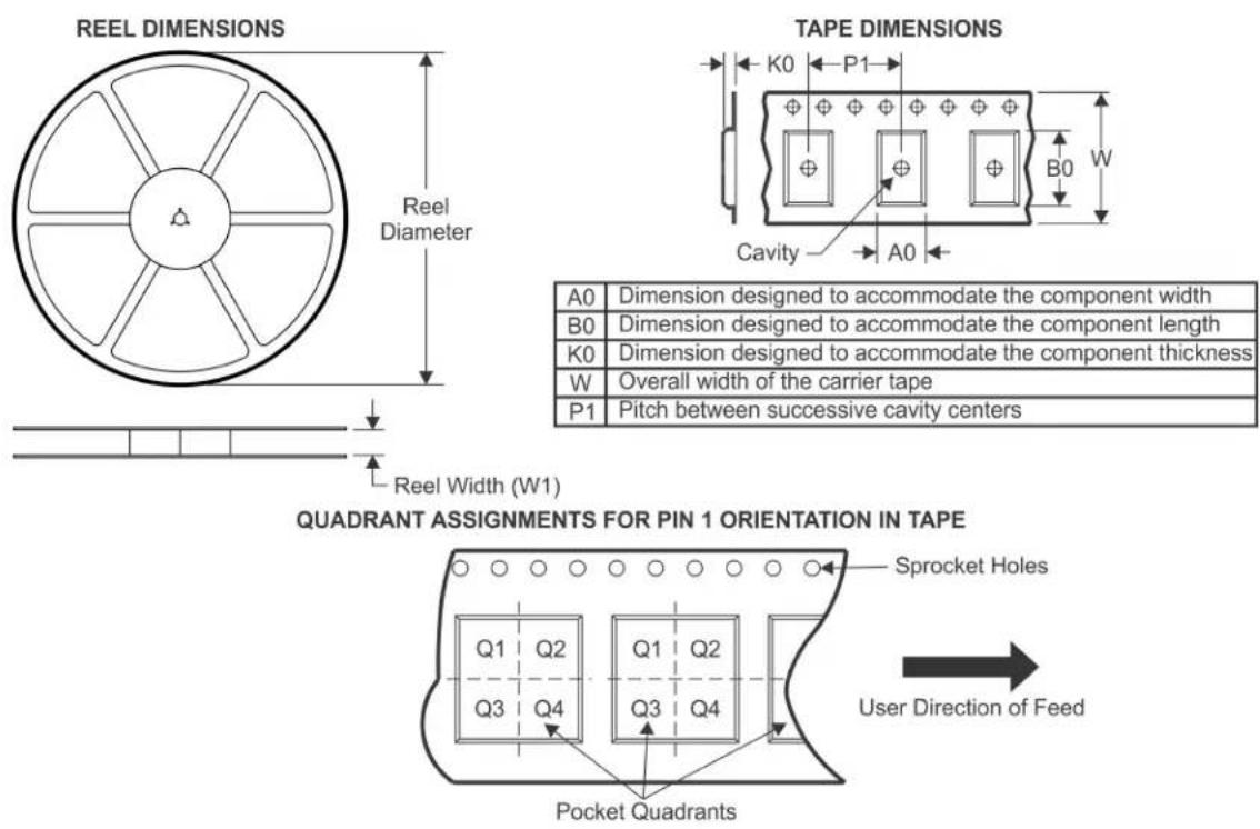
*All dimensions are nominal
| Device Package | Type | Package Drawing | Pins | SPQ Reel | Diameter (mm) | Reel Width W1 (mm) | A0 (mm) | B0 (mm) | K0 (mm) | P1 (mm) | W (mm) | Pin1 Quadrant |
| SN74LS122DR SOIC | D 14 2500 | 330.0 16 | 4 6.5 | 9.0 2.1 8.0 | 16.0 Q1 | |||||||
| SN74LS122NSR SO | NS 14 2000 | 330.0 16 | 4 8.2 | 10.5 2.5 12.0 | 16.0 Q1 | |||||||
| SN74LS123DBR SSO | P DB 16 2 | 000 330.0 | 16.4 8 | .35 6.6 2.4 | 12.0 16.0 | Q1 | ||||||
| SN74LS123DR SOIC | D 16 2500 | 330.0 16 | 4 6.5 | 10.3 2.1 8.0 | 16.0 Q1 | |||||||
| SN74LS123NSR SO | NS 16 2000 | 330.0 16 | 4 8.2 | 10.5 2.5 12.0 | 16.0 Q1 |
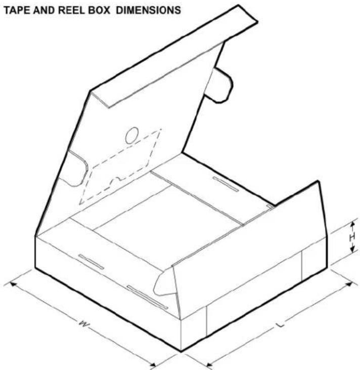
*All dimensions are nominal
| Device | Package Type | Package Drawing | Pins | SPQ | Length (mm) | Width (mm) | Height (mm) |
| SN74LS122DR SOIC | D 14 2500 853.0 449.0 35.0 | ||||||
| SN74LS122NSR SO NS | S 14 2000 853.0 449.0 35.0 | ||||||
| SN74LS123DBR | SSOP | DB 16 2000 | 853.0 449.0 35.0 | ||||
| SN74LS123DR SOIC | D 16 2500 340.5 336.1 32.0 | ||||||
| SN74LS123NSR SO NS | S 16 2000 853.0 449.0 35.0 |
TUBE
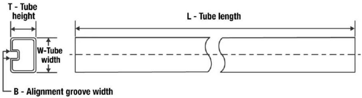
*All dimensions are nominal
| Device | Package Name | Package Type | Pins | SPQ | L (mm) | W (mm) | T (μm) | B (mm) |
| 5962-7603901VFA W CFP 16 1 506.98 26.16 6220 NA | ||||||||
| JM38510/31401B2A FK | LCCC 20 1 506.98 | 2.06 2030 NA | ||||||
| M38510/31401B2A FK | LCCC 20 1 506.98 | 2.06 2030 NA | ||||||
| SN74123N | N | PDIP | 16 | 25 | 506 | 13.97 | 11230 | 4.32 |
| SN74123N | N | PDIP | 16 | 25 | 506 | 13.97 | 11230 | 4.32 |
| SN74LS122D | D | SOIC | 14 | 50 | 506.6 | 8 | 3940 | 4.32 |
| SN74LS122N | N | PDIP | 14 | 25 | 506 | 13.97 | 11230 | 4.32 |
| SN74LS122N | N | PDIP | 14 | 25 | 506 | 13.97 | 11230 | 4.32 |
| SN74LS122NE4 | N | PDIP | 14 | 25 | 506 | 13.97 | 11230 | 4.32 |
| SN74LS122NE4 | N | PDIP | 14 | 25 | 506 | 13.97 | 11230 | 4.32 |
| SN74LS123D | D | SOIC | 16 | 40 | 507 | 8 | 3940 | 4.32 |
| SN74LS123DE4 | D | SOIC | 16 | 40 | 507 | 8 | 3940 | 4.32 |
| SN74LS123DG4 | D | SOIC | 16 | 40 | 507 | 8 | 3940 | 4.32 |
| SN74LS123N | N | PDIP | 16 | 25 | 506 | 13.97 | 11230 | 4.32 |
| SN74LS123N | N | PDIP | 16 | 25 | 506 | 13.97 | 11230 | 4.32 |
| SN74LS123NE4 | N | PDIP | 16 | 25 | 506 | 13.97 | 11230 | 4.32 |
| SN74LS123NE4 | N | PDIP | 16 | 25 | 506 | 13.97 | 11230 | 4.32 |
| SNJ54LS123FK | FK LCCC 20 1 506.98 12.06 2030 NA | |||||||
SOP
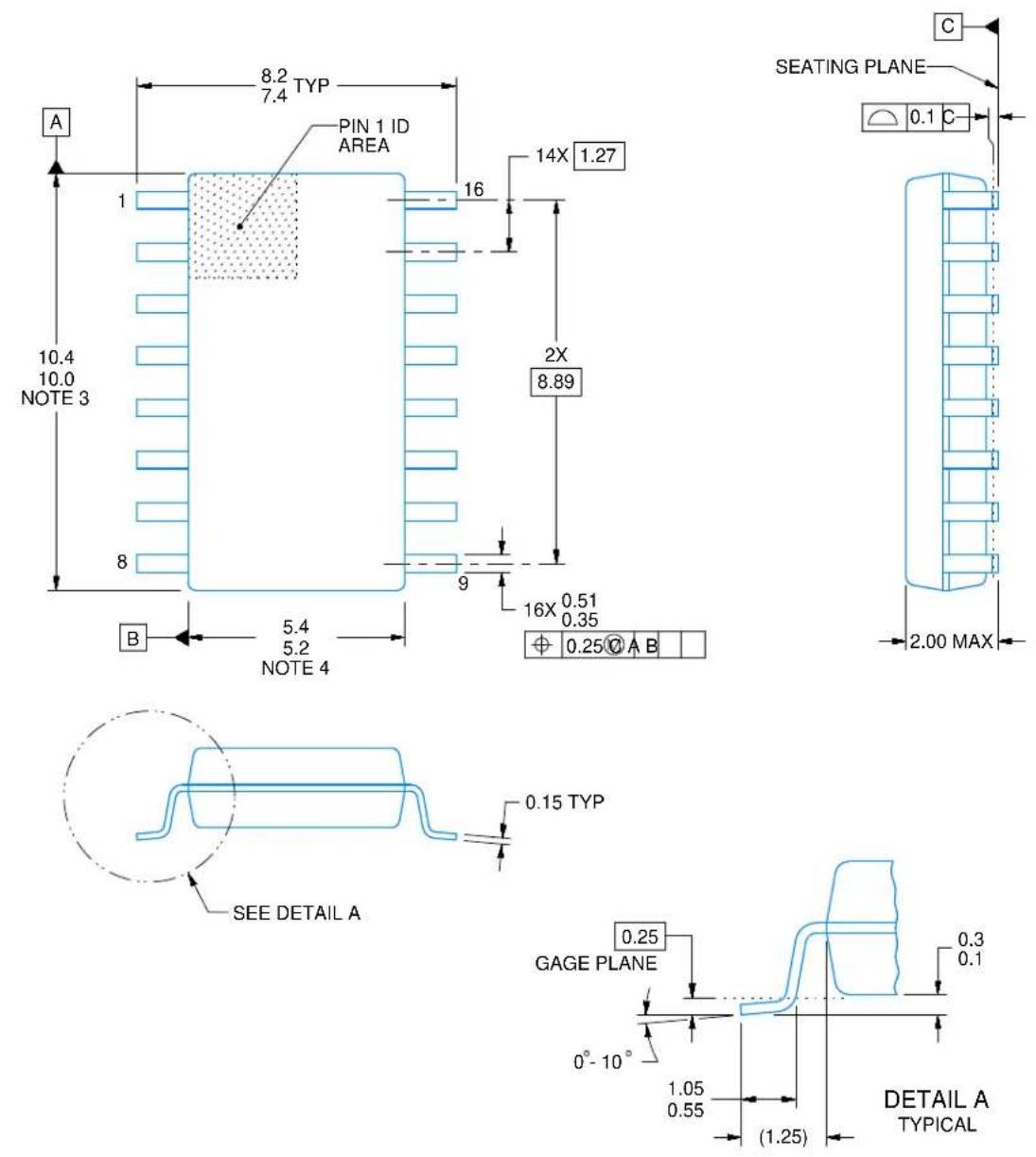
4220735/A 12/2021
NOTES:
- All linear dimensions are in millimeters. Dimensions in parenthesis are for reference only. Dimensioning and tolerancing per ASME Y14.5M.
- This drawing is subject to change without notice.
- This dimension does not include mold flash, protrusions, or gate burrs. Mold flash, protrusions, or gate burrs shall not exceed 0.15 mm, per side.
- This dimension does not include interlead flash. Interlead flash shall not exceed 0.25 mm, per side.
SOP
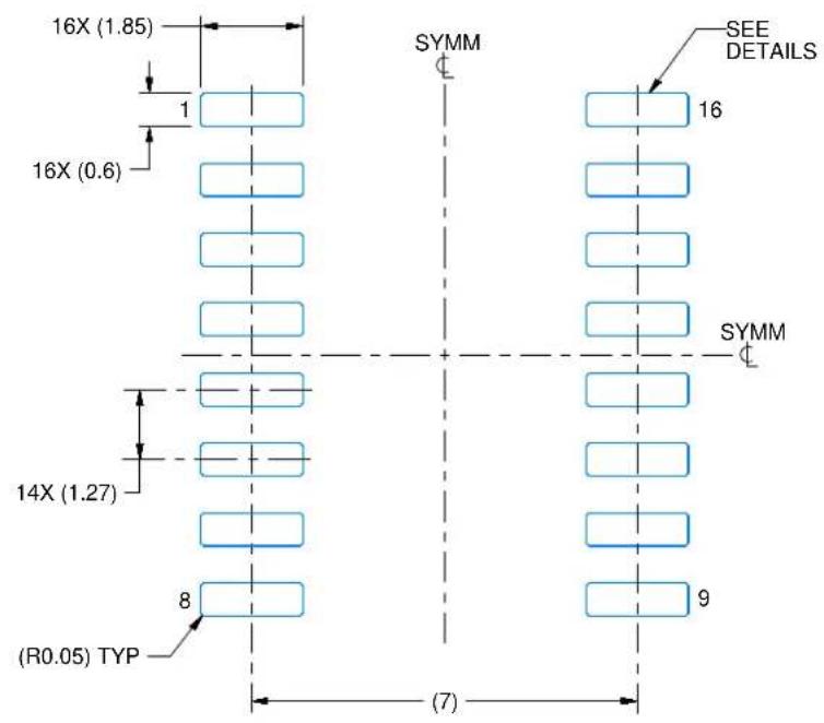
LAND PATTERN EXAMPLE SCALE:7X
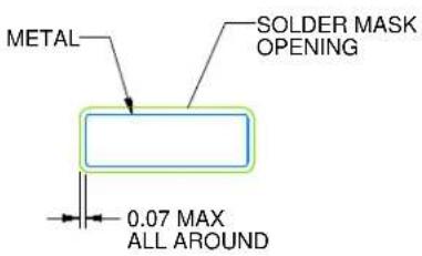
NON SOLDER MASK DEFINED
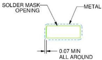
SOLDER MASK
DEFINED
SOLDER MASK DETAILS
4220735/A 12/2021
NOTES: (continued)
- Publication IPC-7351 may have alternate designs.
- Solder mask tolerances between and around signal pads can vary based on board fabrication site.
SOP
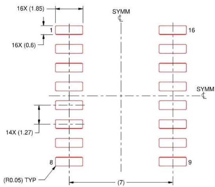
SOLDER PASTE EXAMPLE BASED ON 0.125 mm THICK STENCIL SCALE:7X
4220735/A 12/2021
NOTES: (continued)
- Laser cutting apertures with trapezoidal walls and rounded corners may offer better paste release. IPC-7525 may have alternate design recommendations.
- Board assembly site may have different recommendations for stencil design.
FK (S-CQCC-N**)
28 TERMINAL SHOWN
LEADLESS CERAMIC CHIP CARRIER
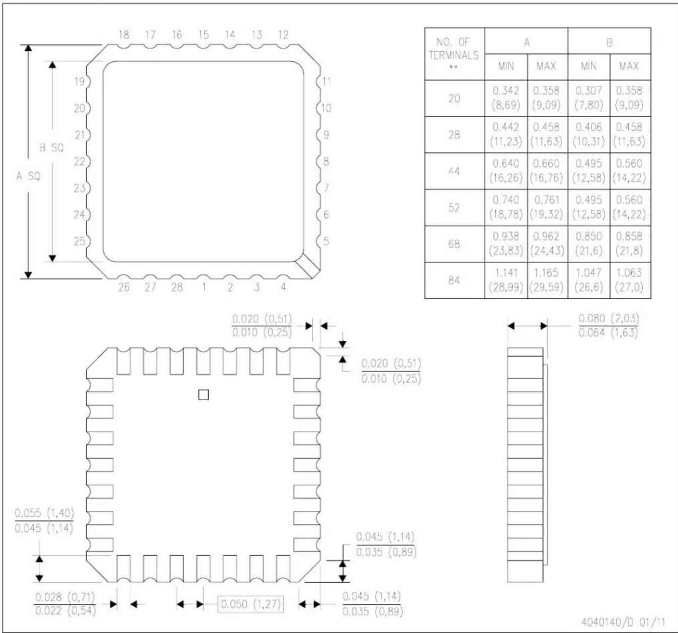
| NO. OF TERMINALS** | A | B | ||
| MIN | MAX | MIN | MAX | |
| 20 | 0.342(8,69) | 0.358(9,09) | 0.307(7,80) | 0.358(9,09) |
| 28 | 0.442(11,23) | 0.458(11,63) | 0.406(10,31) | 0.458(11,63) |
| 44 | 0.640(16,26) | 0.660(16,76) | 0.495(12,58) | 0.560(14,22) |
| 52 | 0.740(18,78) | 0.761(19,32) | 0.495(12,58) | 0.560(14,22) |
| 68 | 0.938(23,83) | 0.962(24,43) | 0.850(21,6) | 0.858(21,8) |
| 84 | 1.141(28,99) | 1.165(29,59) | 1.047(26,6) | 1.063(27,0) |
4040140/D 01/11
NOTES: A. All linear dimensions are in inches (millimeters).
B. This drawing is subject to change without notice.
C. This package can be hermetically sealed with a metal lid.
D. Falls within JEDEC MS-004
D (R-PDSO-G16)
PLASTIC SMALL OUTLINE
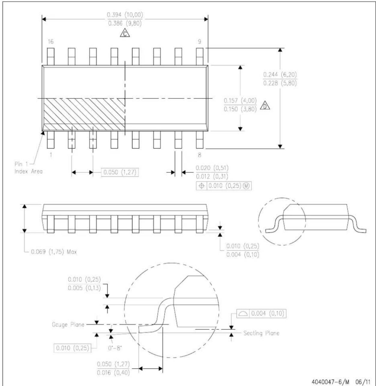
NOTES: A. All linear dimensions are in inches (millimeters).
B. This drawing is subject to change without notice.
Body length does not include mold flash, protrusions, or gate burrs. Mold flash, protrusions, or gate burrs shall not exceed 0.006 (0,15) each side.
Body width does not include interlead flash. Interlead flash shall not exceed 0.017 (0,43) each side.
E. Reference JEDEC MS-012 variation AC.
D (R-PDSO-G16)
NOTES: A. All linear dimensions are in millimeters.
B. This drawing is subject to change without notice.
C. Publication IPC-7351 is recommended for alternate designs.
D. Laser cutting apertures with trapezoidal walls and also rounding corners will offer better paste release. Customers should contact their board assembly site for stencil design recommendations. Refer to IPC-7525 for other stencil recommendations.
E. Customers should contact their board fabrication site for solder mask tolerances between and around signal pads.
SMALL OUTLINE PACKAGE
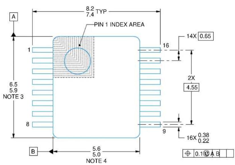
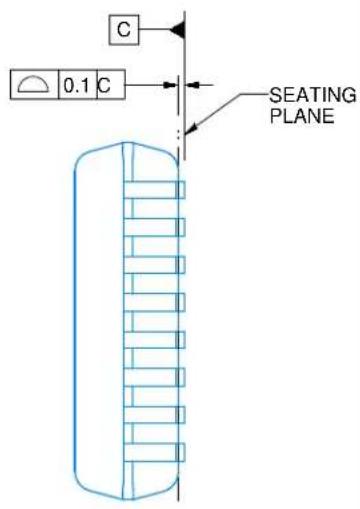
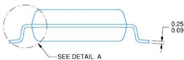
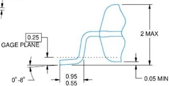
DETAIL A TYPICAL
4220763/A 05/2022
NOTES:
- All linear dimensions are in millimeters. Any dimensions in parenthesis are for reference only. Dimensioning and tolerancing per ASME Y14.5M.
- This drawing is subject to change without notice.
- This dimension does not include mold flash, protrusions, or gate burrs. Mold flash, protrusions, or gate burrs shall not exceed 0.15 mm per side.
- Reference JEDEC registration MO-150.
SMALL OUTLINE PACKAGE
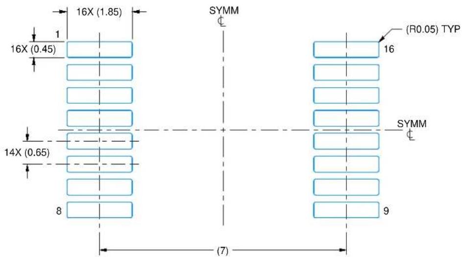
LAND PATTERN EXAMPLE
EXPOSED METAL SHOWN
SCALE: 10X
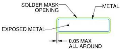
NON-SOLDER MASK
DEFINED
(PREFERRED)
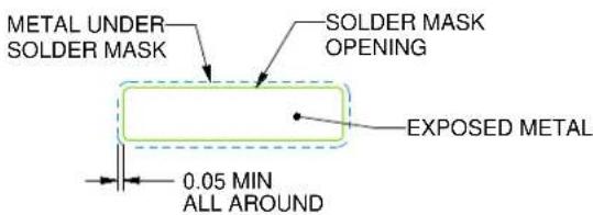
SOLDER MASK
DEFINED
SOLDER MASK DETAILS
4220763/A 05/2022
NOTES: (continued)
- Publication IPC-7351 may have alternate designs.
- Solder mask tolerances between and around signal pads can vary based on board fabrication site.
SMALL OUTLINE PACKAGE
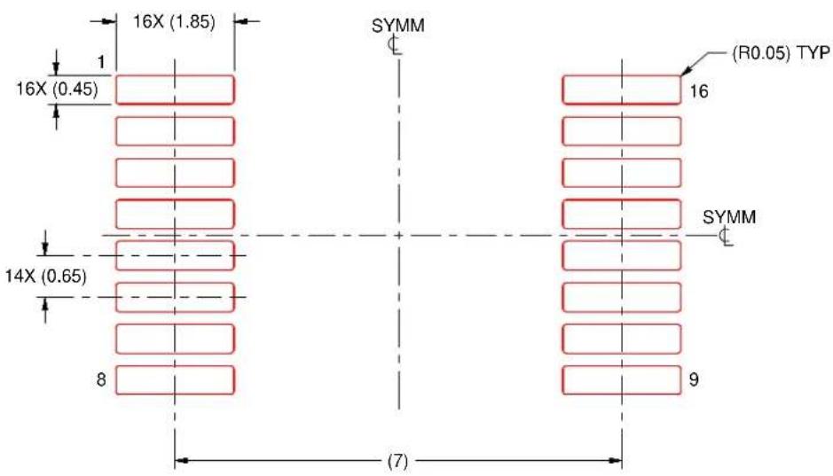
SOLDER PASTE EXAMPLE
BASED ON 0.125 mm THICK STENCIL
SCALE: 10X
4220763/A 05/2022
NOTES: (continued)
- Laser cutting apertures with trapezoidal walls and rounded corners may offer better paste release. IPC-7525 may have alternate design recommendations.
- Board assembly site may have different recommendations for stencil design.
MECHANICAL DATA
NS (R-PDSO-G\*\*)
PLASTIC SMALL-OUTLINE PACKAGE
14-PINS SHOWN
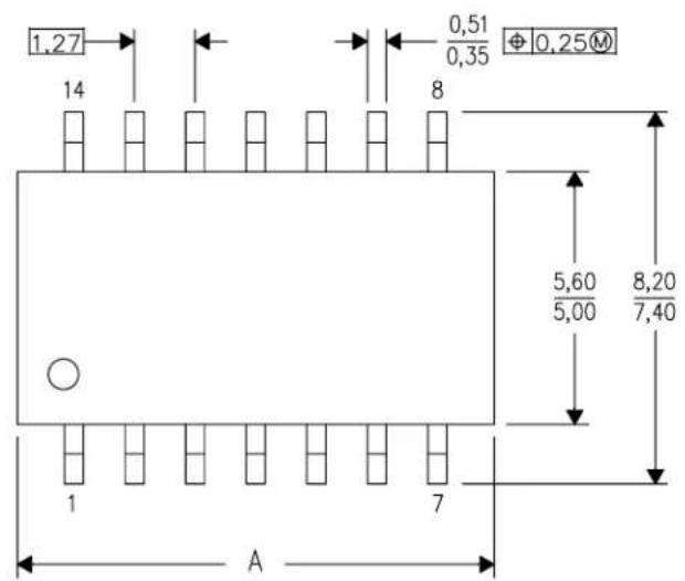
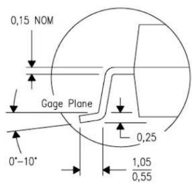
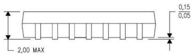
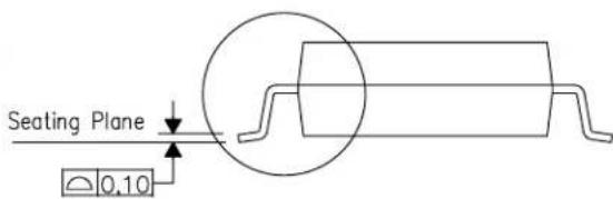
| DIM\PINS ** | 14 | 16 | 20 | 24 |
| A MAX | 10,50 | 10,50 | 12,90 | 15,30 |
| A MIN | 9,90 | 9,90 | 12,30 | 14,70 |
4040062/C 03/03
NOTES: A. All linear dimensions are in millimeters.
B. This drawing is subject to change without notice.
C. Body dimensions do not include mold flash or protrusion, not to exceed 0,15.
W (R-GDFP-F16)
CERAMIC DUAL FLATPACK
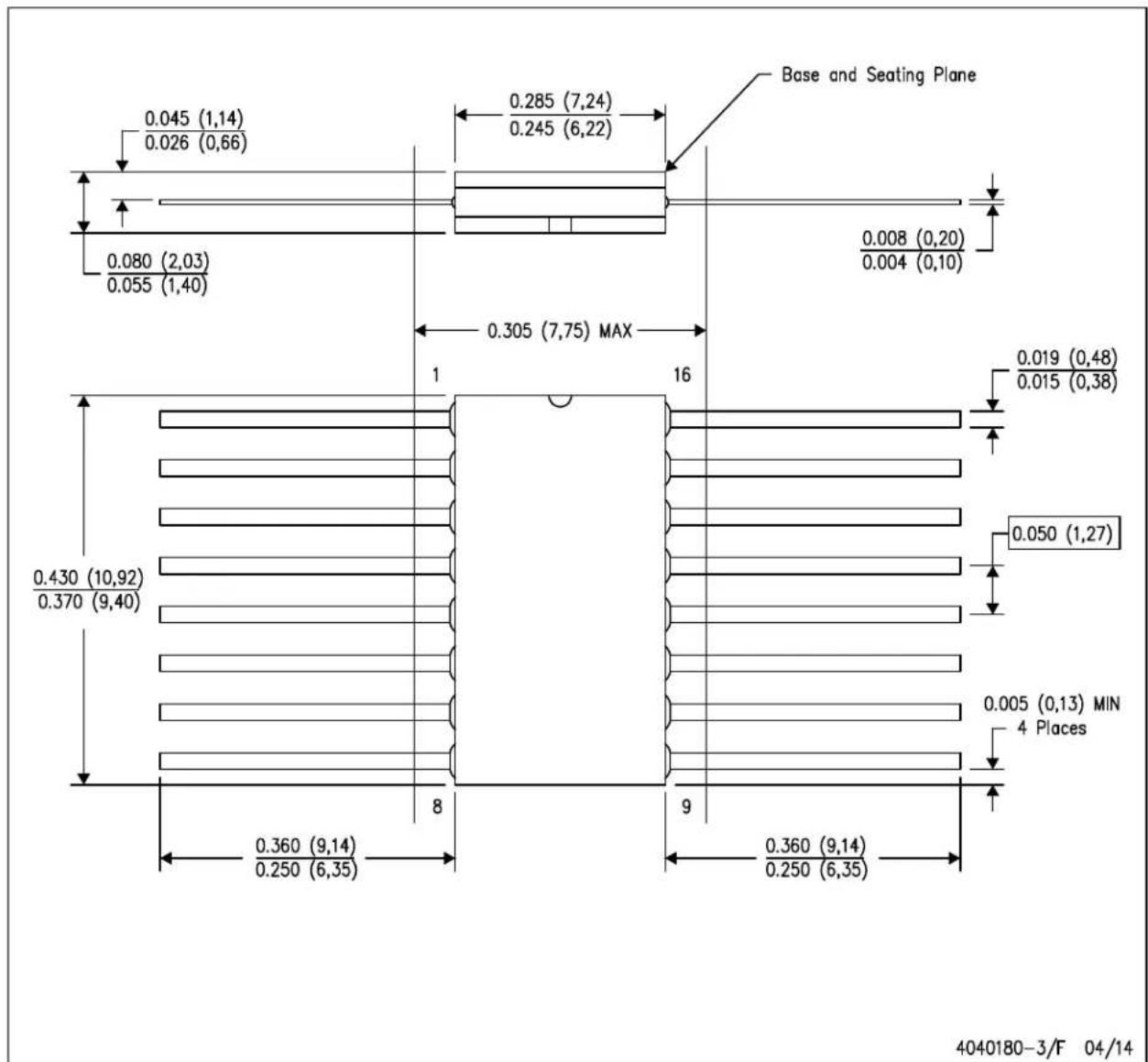
other
| Dimension | Value | | ----------------- | ------- | | Base and Seating Plane | 0.285 (7,24) | | Base and Seating Plane | 0.245 (6,22) | | Base and Seating Plane | 0.080 (2,03) | | Base and Seating Plane | 0.055 (1,40) | | Base and Seating Plane | 0.305 (7,75) MAX | | Base and Seating Plane | 0.008 (0,20) | | Base and Seating Plane | 0.004 (0,10) | | Base and Seating Plane | 0.430 (10,92) | | Base and Seating Plane | 0.370 (9,40) | | Base and Seating Plane | 0.360 (9,14) | | Base and Seating Plane | 0.250 (6,35) | | Base and Seating Plane | 0.360 (9,14) | | Base and Seating Plane | 0.250 (6,35) | | Base and Seating Plane | 0.019 (0,48) | | Base and Seating Plane | 0.015 (0,38) | | Base and Seating Plane | 0.050 (1,27) | | Base and Seating Plane | 0.005 (0,13) MIN 4 Places | 4040180–3/F 04/14NOTES: A. All linear dimensions are in inches (millimeters).
B. This drawing is subject to change without notice.
C. This package can be hermetically sealed with a ceramic lid using glass frit.
D. Index point is provided on cap for terminal identification only.
E. Falls within MIL STD 1835 GDFP2-F16
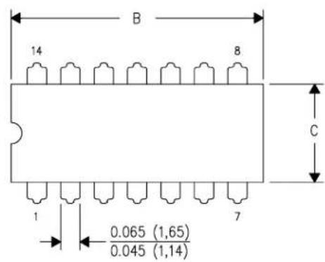
| PINS **DIM | 14 | 16 | 18 | 20 |
| A | 0.300(7,62)BSC | 0.300(7,62)BSC | 0.300(7,62)BSC | 0.300(7,62)BSC |
| B MAX | 0.785(19,94) | .840(21,34) | 0.960(24,38) | 1.060(26,92) |
| B MIN | — | — | — | — |
| C MAX | 0.300(7,62) | 0.300(7,62) | 0.310(7,87) | 0.300(7,62) |
| C MIN | 0.245(6,22) | 0.245(6,22) | 0.220(5,59) | 0.245(6,22) |
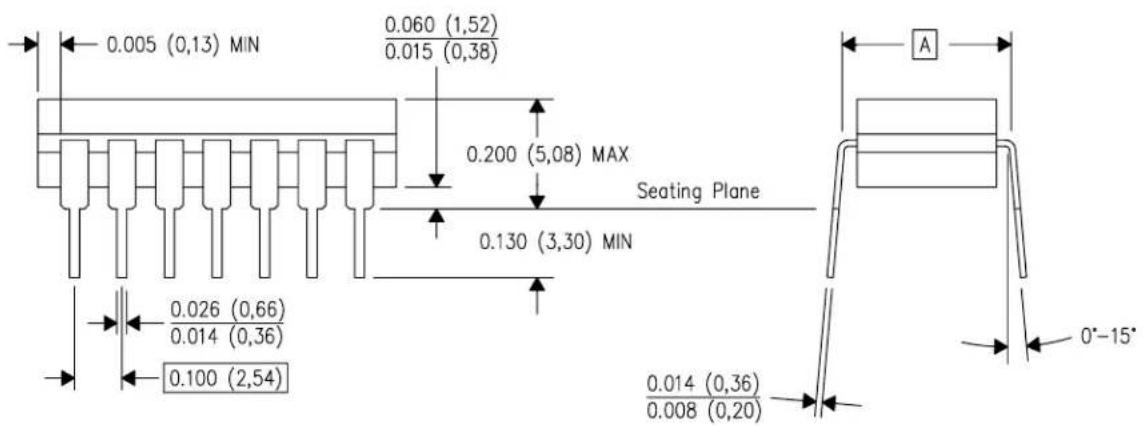
4040083/F 03/03
NOTES:
A. All linear dimensions are in inches (millimeters).
B. This drawing is subject to change without notice.
C. This package is hermetically sealed with a ceramic lid using glass frit.
D. Index point is provided on cap for terminal identification only on press ceramic glass frit seal only.
E. Falls within MIL STD 1835 GDIP1-T14, GDIP1-T16, GDIP1-T18 and GDIP1-T20.
D (R-PDSO-G14)
PLASTIC SMALL OUTLINE
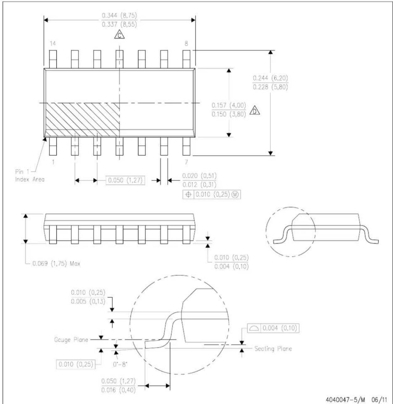
NOTES: A. All linear dimensions are in inches (millimeters).
B. This drawing is subject to change without notice.
Body length does not include mold flash, protrusions, or gate burrs. Mold flash, protrusions, or gate burrs shall not exceed 0.006 (0,15) each side.
Body width does not include interlead flash. Interlead flash shall not exceed 0.017 (0,43) each side.
E. Reference JEDEC MS-012 variation AB.
D (R-PDSO-G14)
4211283-3/E 08/12
NOTES: A. All linear dimensions are in millimeters.
B. This drawing is subject to change without notice.
C. Publication IPC-7351 is recommended for alternate designs.
D. Laser cutting apertures with trapezoidal walls and also rounding corners will offer better paste release. Customers should contact their board assembly site for stencil design recommendations. Refer to IPC-7525 for other stencil recommendations.
E. Customers should contact their board fabrication site for solder mask tolerances between and around signal pads.
N (R-PDIP-T\*\*)
16 PINS SHOWN
PLASTIC DUAL-IN-LINE PACKAGE
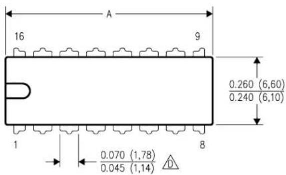
C
| DIM\PINS ** | 14 | 16 | 18 | 20 |
| A MAX | 0.775(19,69) | 0.775(19,69) | 0.920(23,37) | 1.060(26,92) |
| A MIN | 0.745(18,92) | 0.745(18,92) | 0.850(21,59) | 0.940(23,88) |
| MS-001VARIATION | AA | BB | AC | AD |
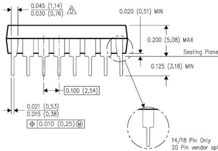
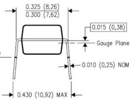
4040049/E 12/2002
NOTES: A. All linear dimensions are in inches (millimeters).
B. This drawing is subject to change without notice.
C Falls within JEDEC MS-001, except 18 and 20 pin minimum body length (Dim A).
The 20 pin end lead shoulder width is a vendor option, either half or full width.
IMPORTANT NOTICE AND DISCLAIMER
TI PROVIDES TECHNICAL AND RELIABILITY DATA (INCLUDING DATA SHEETS), DESIGN RESOURCES (INCLUDING REFERENCE DESIGNS), APPLICATION OR OTHER DESIGN ADVICE, WEB TOOLS, SAFETY INFORMATION, AND OTHER RESOURCES "AS IS" AND WITH ALL FAULTS, AND DISCLAIMS ALL WARRANTIES, EXPRESS AND IMPLIED, INCLUDING WITHOUT LIMITATION ANY IMPLIED WARRANTIES OF MERCHANTABILITY, FITNESS FOR A PARTICULAR PURPOSE OR NON-INFRINGEMENT OF THIRD PARTY INTELLECTUAL PROPERTY RIGHTS.
These resources are intended for skilled developers designing with TI products. You are solely responsible for (1) selecting the appropriate TI products for your application, (2) designing, validating and testing your application, and (3) ensuring your application meets applicable standards, and any other safety, security, regulatory or other requirements.
These resources are subject to change without notice. TI grants you permission to use these resources only for development of an application that uses the TI products described in the resource. Other reproduction and display of these resources is prohibited. No license is granted to any other TI intellectual property right or to any third party intellectual property right. TI disclaims responsibility for, and you will fully indemnify TI and its representatives against, any claims, damages, costs, losses, and liabilities arising out of your use of these resources.
TI's products are provided subject to TI's Terms of Sale or other applicable terms available either on ti.com or provided in conjunction with such TI products. TI's provision of these resources does not expand or otherwise alter TI's applicable warranties or warranty disclaimers for TI products.
TI objects to and rejects any additional or different terms you may have proposed.
Mailing Address: Texas Instruments, Post Office Box 655303, Dallas, Texas 75265
Copyright © 2022, Texas Instruments Incorporated

- description
- description (continued)
- absolute maximum ratings over operating free-air temperature range (unless otherwise noted)
- TYPICAL APPLICATION DATA FOR '122, '123, '130
- TYPICAL APPLICATION DATA FOR 'LS122, 'LS123
- PACKAGE OPTION ADDENDUM
- TUBE
- NOTES:
- MECHANICAL DATA
- NS (R-PDSO-G\*\*)
- PLASTIC SMALL-OUTLINE PACKAGE
- N (R-PDIP-T\*\*)
- PLASTIC DUAL-IN-LINE PACKAGE
- IMPORTANT NOTICE AND DISCLAIMER
Brand : TEXAS INSTRUMENTS
Model : SN74LS122N
Category : Processor