
MODBUSCARD - Regulator Tripp Lite - Free user manual and instructions
Find the device manual for free MODBUSCARD Tripp Lite in PDF.


| Product Type | Communication Card |
| Brand | Tripp Lite |
| Model | MODBUSCARD |
| Compatibility | Select Tripp Lite UPS Systems with SNMP/COM slot |
| Interface | MODBUS RTU via RS-485 |
| Dimensions (W x H x D) | 2.4 x 0.8 x 3.4 in. (61 x 20 x 86 mm) |
| Weight | 1.1 oz. (31 g) |
| Power Source | Powered by UPS (no external power required) |
| Functions | Remote monitoring, control, and configuration via MODBUS protocol |
| Installation | Internal slot in compatible UPS |
| Supported Registers | Voltage, frequency, load, battery status, alarms, and more |
| Baud Rate | 9600 or 19200 bps (configurable) |
| Protocol | MODBUS RTU |
| Certifications | CE, FCC |
| Operating Temperature | 32°F to 104°F (0°C to 40°C) |
| Humidity | 0% to 95% non-condensing |
| Maintenance | No user-serviceable parts; do not attempt to open |
| Safety | Install only in compatible UPS; follow UPS manual |
| Spare Parts | Contact Tripp Lite for replacement |
| Repairability | Not user-repairable; replace if defective |
Frequently Asked Questions - MODBUSCARD Tripp Lite
User questions about MODBUSCARD Tripp Lite
0 question about this device. Answer the ones you know or ask your own.
Ask a new question about this device
Download the instructions for your Regulator in PDF format for free! Find your manual MODBUSCARD - Tripp Lite and take your electronic device back in hand. On this page are published all the documents necessary for the use of your device. MODBUSCARD by Tripp Lite.
USER MANUAL MODBUSCARD Tripp Lite
Warranty and Product Registration 20
PROTECT YOUR INVESTMENT!
Register your product for quicker service and ultimate peace of mind.
You could also win an ISOBAR6ULTRA surge protector—a \$100 value!
www.tripplite.com/warranty




Introduction
The MODBUSCARD provides a compatible SmartOnline® UPS system communication functionality with a PC by way of the MODBUS protocol.
Features
- Implements MODBUS protocol
- Provides MODBUS functions, including Read Coils, Discrete Inputs, Holding Registers, Input Registers, Write Single Coils and Write Single Registers
- Provides communication through RS-232, RS-485 or RS-422 interfaces
- Simultaneous communication through RS-232 and RS-485, or RS-232 and RS-422 connection interfaces
Configuration
A MODBUS Device ID Configuration Switches (SW1)
B RS-232 Port Configuration Switches (SW2)
C RS-422/485 Port Configuration Switches (SW3)
D RS-422/485 Communication Mode Switch (SW4)
E Terminal Strip Connections for RS-232/422/485 Communication
F Diagnostic LEDs

Configuration
Communication Terminal Strip Wiring Pinouts
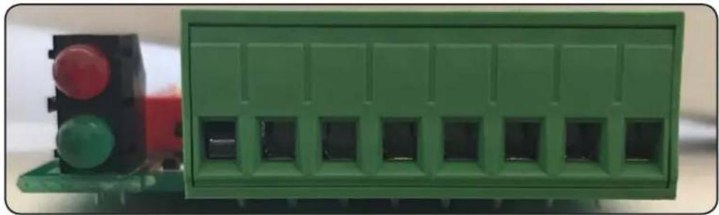
MODBUSCARD Communication Terminal Pinout
| RS-232 RS-485 | |||||||
| GND Rx Tx | GND T-T+ | ||||||
| 8765 | 4321 | ||||||
| GND R-R+ T-T+RS-422 | |||||||
For RS-232 connection, use terminals 6 (Tx), 7 (Rx), 8 (G).
For RS-485, use terminals 1 (T+), 2 (T-), 5 (G) for half-duplex communication.
For RS-422, use terminals 1 (T+), 2 (T-), 3 (R+), 4 (R-), 5 (G) for full-duplex communication.
Note: The communication methods chosen must have its configuration dip switches set prior to installing the MODBUSCARD into the UPS systems accessory slot.

Device ID Configuration
Every MODBUS device needs to be set to a specific ID in order to be recognized by the system monitoring its MODBUS communication. Each switch of SW1 has a specific value assigned to it. The MODBUSCARD supports device IDs from 0-255, starting from the Least Significant Bit (LSB) to the Most Significant Bit (MSB). See Device ID Switch Values (Figure A).

Figure A: Device ID Switch Values (SW1)
Configuration
MODBUS DEVICE ID = 0 (Default)

MODBUS ID = 1

MODBUS ID = 21

MODBUS ID = 200

Figure B: Device ID Configuration Examples
Configuration of RS-232 Port
Use SW2 to configure the RS-232 interface.
| Pin Function | |
| 6 Card TxD - transfer data to PC | |
| 7 Card RxD - receive data from PC | |
| 8 GND | |
| Function Switch Value | |||
| ON/OFF | SW-1 SW-2 | ||
| OFF OFF MODBUS | OFF | ||
| ON ON MODBUS ON | |||
| Baud-Rate | SW2-1 SW2-2 | ||
| OFF OFF 2400 (Default) | |||
| ON OFF 4800 | |||
| OFF ON 9600 | |||
| ON ON 19200 | |||
| Parity Check | SW2-3 | OFF Disable Parity Check (Default) | |
| ON Enable Parity Check | |||
| SW2-4 | OFF Even Parity (Default) | ||
| ON Odd Parity | |||
| Protocol | SW2-5 SW2-6 | ||
| OFF OFF MODBUS | Protocol (Default) | ||
| ON OFF Regular Protocol | |||
| OFF ON 3-Phase Protocol | |||
| SW2-7 Reserved | |||
| SW2-8 Reserved | |||
Configuration
Configuration of RS-422/485 Port
Use SW3 to configure the RS-422/485 interface.
| Pin Function | |
| 1 Card D+ (T+) | |
| 2 Card D- (T-) | |
| 3 Card R+ | |
| 4 Card R- |
| Switch Setting Function | ||
| SW4 | RS-485 Enable RS-485 | |
| RS-422 Enable RS-422 | ||
| Function Switch Value | |||
| Baud-Rate | SW3-1 SW3-2 | ||
| OFF OFF 2400 (Default) | |||
| ON OFF 4800 | |||
| OFF ON 9600 | |||
| ON ON 19200 | |||
| Parity Check | SW3-3 | OFF Disable Parity Check (Default) | |
| ON Enable Parity Check | |||
| SW3-4 | OFF Even Parity (Default) | ||
| ON Odd Parity | |||
| Protocol | SW3-5 SW3-6 | ||
| OFF OFF MODBUS Protocol (Default) | |||
| ON OFF Regular Protocol | |||
| OFF ON 3-Phase Protocol | |||
| Termination Resistor | SW3-7 | OFF Disable RS-485/422 Termination Resistor (Default) | |
| ON Enable RS-485/422 Termination Resistor | |||
| SW3-8 | OFF Disable RS-422 Termination Resistor (Default) | ||
| ON Enable RS-422 Termination Resistor | |||
Installation
The MODBUSCARD should be installed in the accessory slot of a compatible SmartOnline UPS system.
Note: Prior to installing the card into the UPS, all configuration switches should be set to the values required by the UPS and your PC communication ports.
- Remove the screws securing the blank cover plate from the UPS and set them aside.
- Detach the communication terminal connector from the MODBUSCARD.
- Slide the configured MODBUSCARD into the UPS accessory slot
- With the screws that were removed in step 1, attach the compatible cover plate that came with MODBUSCARD to the accessory slot mounting points.
- Re-insert the wired terminal strip connector into the MODBUSCARD port.
- The MODBUSCARD's red LED will flash to indicate the UPS is connected and ready for communication.
- The user will need to supply the means of communication on the PC side via RS-232, RS-422, or RS-485, as well as the appropriate monitoring software.
Operation
LED Indicators
| LED Status Description | ||
| RED | OFF UPS disconnected | |
| Flashing (1 second) UPS connected | ||
| GREEN Illuminated (0.2 seconds) Receiving PC request | ||
Discrete Inputs (Range 0x0100 - 0x012F, Read Function 0x02)
The Read Discrete Inputs function code is used to read 1-2000 contiguous status of Discrete Inputs in a remote device. The starting address and number of inputs is specified by the request Protocol Data Unit. Addresses start at 0 and Discrete Inputs numbered 1-16 would address as 0-15.
| Description Address Value 0 Value 1 | |||
| Alarm Temperature 0x0100 OK Over Temperature | |||
| Alarm Input Bad | 0x0101 OK Input Bad | ||
| Alarm Output Bad | 0x0102 OK Output Bad | ||
| Alarm Overload | 0x0103 OK Overload | ||
| Alarm Bypass Bad | 0x0104 OK Bypass Bad | ||
| Alarm Output Off | 0x0105 Output On Output Off | ||
| Alarm UPS Shutdown | 0x0106 OK Shutdown | ||
| Alarm Charger Failure | 0x0107 OK Charger Failure | ||
| Alarm System Off 0x0108 System On | System Off | ||
| Alarm Fan Failure 0x0109 OK Fan Failure | |||
| Alarm Fuse Failure | 0x010A | OK Fuse Failure | |
| Alarm General Fault | 0x010B OK General Fault | ||
| Alarm Awaiting Power | 0x010C OK Awaiting Power | ||
| Alarm Shutdown Pending | 0x010D | OK Shutdown Pending | |
| Alarm Shutdown Imminent | 0x010E | OK Shutdown Imminent | |
| Buzzer Status | 0x010F | Silence | Alarm |
| Economy Mode | 0x0110 | No | Yes |
| Alarm Inverter Bad | 0x0111 OK Inverter Bad | ||
| Emergency Power Off | 0x0112 Off | On | |
| Buzzer State | 0x0113 Disable | Enable | |
| Battery Ground Fault | 0x0114 OK Battery Ground Fault | ||
| Reserved | 0x0115 | ||
| Reserved | 0x0116 | ||
Operation
| Description Address Value 0 Value 1 | |||
| Reserved 0x0117 | |||
| Alarm Rectifier Main Fail 0x0118 OK Rectifier Main Fail | |||
| Alarm Rectifier Hi DC Stop 0x0119 OK Rectifier Hi DC Stop | |||
| Alarm Over Temp or Fuse Fail 0x011A OK Over Temp or Fuse | Fail | ||
| Alarm Battery Low 0x011B OK Battery Low | |||
| Alarm Battery Low Stop 0x011C OK Battery Low Stop | |||
| Alarm Battery Ground Fault 0x011D OK Battery Ground Fault | |||
| Inverter On 0x011E Inverter Off | Inverter ON | ||
| Alarm Inverter Overload | 0x011F | OK Inverter Overload | |
| Alarm Inverter Abnormal | 0x0120 OK Inverter Abnormal | ||
| Alarm Load on Reserve | 0x0121 Load Not On Reserve | Load on Reserve | |
| Alarm Reserve Mains Fail | 0x0122 OK Reserve Mains Fail | ||
| Alarm Reserve Freq. Abnormal | 0x0123 OK Reserve Freq. Abnormal | ||
| Alarm Test In Progress | 0x0124 No Test In Progress | Test In Progress | |
| Alarm Test Error | 0x0125 No Test Error | Test Error | |
| UPS In Sleep Mode | 0x0126 UPS Not In Sleep Mode | UPS In Sleep Mode | |
| Reserved 0x0127 | |||
| Alarm Bypass Volt/Freq Bad | 0x0128 OK Bypass Volt/Freq Bad | ||
| Alarm Bypass Phase Sequence Bad | 0x0129 OK Bypass Phase Sequence Bad | ||
| Alarm Bypass STS Overload | 0x012A OK Bypass STS Overload | ||
| Alarm Bypass STS Over | 0x012B OK Bypass STS Over | ||
| Alarm Bypass STS Fault | 0x012C OK Bypass STS Fault | ||
| Reserved 0x012D | |||
| Reserved 0x012E | |||
| Reserved 0x012F |
Note: Your UPS may not support all fields.
Coils (Range 0x0200 - 0x020F, Read Function 0x01, Write Function 0x05)
The Read Coils function reads 1-2000 contiguous status of coils in a remote device. The starting address and number of coils is specified by the request Protocol Data Unit. Addresses start at 0 and Coils numbered 1-16 would address as 0-15.
The Write Coils function writes a single output to ON/OFF in a remote device. A specified constant in the data field requests the ON/OFF state. Addresses start at 0 and Coils numbered 1 would address as 0.
| Description Address Value 0 Value 1 | |||
| UPS Buzzer | 0x0200 Silence | Alarm | |
| Shutdown Type | 0x0201 UPS Output | UPS System | |
| Economy Mode Setting | 0x0202 Disable | Enable | |
| ATX PC Reboot Function | 0x0203 Disable | Enable | |
| AC Fail & Restore Auto-Reboot | 0x0204 Disable | Enable | |
| ATX PC Resume Function | 0x0205 Disable | Enable | |
| Enable/Disable Inverter | 0x0206 Disable | Enable | |
| EPO Setting | 0x0207 Disable | Enable | |
| Enable/Disable Inverter | 0x0208 Disable | Enable | |
| Clear SRAM | 0x0209 Clear SRAM | Clear SRAM | |
| Cancel Shutdown Restart | 0x020A | Cancel Shutdown Restart | Cancel Shutdown Restart |
| Set Output On/Off | 0x020B OFF | ON | |
| Reserved 0x020C | |||
| Reserved 0x020D | |||
| Reserved 0x020E | |||
| Reserved 0x020F | |||
Note: Your UPS may not support all fields.
Operation
Holding Register (Range 0x0300 - 0x0321, Read Function 0x03, Write Function 0x06)
The Read Holding Registers function code is used to read contents of a contiguous block of Holding Registers in a remote device. Starting register address and number of registers is specified by the request Protocol Data Unit. Addresses start at 0 and registers numbered 1-16 address as 0-15.
The Write Single Register function code is used to write a Single Holding Register in a remote device. The address of the register to be written is specified by the request Protocol Data Unit. Addresses start at 0 and registers numbered 1 address as 0.
| Description Address Value Unit | |||
| Shutdown Action 0x0300 0-999 (0=Abort) Seconds | |||
| Shutdown Restart 0x0301 0-65535 Minutes | |||
| Test 0x0302 | 0: Abort Test | ||
| 1: General Test | |||
| 2: BTV Test | |||
| 3: Test for 10 seconds | |||
| 4: Test until battery low | |||
| UPS Identification 0x0303 0-99 | |||
| Low Transfer Voltage 0x0304 0-999 Voltage | |||
| High Transfer Voltage 0x0305 0-999 Voltage | |||
| Voltage Sensitivity 0x0306 | 0: Normal | ||
| 1: Reduced | |||
| 2: Low | |||
| Last Battery Replace Date-Year 0x0307 0-9999 | |||
| Last Battery Replace Date-Month | 0x0308 1-12 | ||
| Last Battery Replace Date-Day | 0x0309 1-31 | ||
| Next Battery Replace Date-Year | 0x030A | 0-9999 | |
| Next Battery Replace Date-Month | 0x030B 1-12 | ||
| Next Battery Replace Date-Day | 0x030C 1-31 | ||
| Description | Address | Value | Unit |
| UPS Periodic Auto-Test | 0x030D | 1: Disable | |
| 2: Daily | |||
| 3: Weekly | |||
| 4: Bi-Weekly | |||
| 5: Monthly | |||
| Buzzer Test | 0x030E | 1-99 | Seconds |
| UPS Boot Delay | 0x030F | 0-999 Seconds | |
| Bypass Freq. Tolerance | 0x0310 5-50 | 0.1 Hz | |
| Select Output Voltage | 0x0311 0-999 Voltage | ||
| Test Time | 0x0312 1-60 | Minutes | |
| Test Voltage | 0x0313 0-999 Voltage | ||
| Reserved | 0x0314 | ||
| Reserved | 0x0315 | ||
| External Battery Pack | 0x0316 0-10 | ||
| Dry Contact W1 | 0x0317 | ||
| Dry Contact W2 | 0x0318 | ||
| Dry Contact W3 | 0x0319 | ||
| Dry Contact W4 | 0x031A | ||
| Dry Contact W5 | 0x031B | ||
| Dry Contact W6 | 0x031C | ||
| Bypass Low Transfer Voltage | 0x031D | 0-999 Voltage | |
| Bypass High Transfer Voltage | 0x031E | 0-999 Voltage | |
| Bypass Voltage Tolerance | 0x031F | 0-999 Voltage | |
Operation
| Description Address Value Unit | |||
| Dry Contact Input Status 1 0x0320 | |||
| Dry Contact Input Status 2 0x0321 |
Note: Your UPS may not support all fields.
Input Register (Range 0x0400 - 0x051C, Read Function 0x04) Rating Value
The Read Input Registers function code is used to read 1-125 contiguous input registers in a remote device. The starting register address and number of registers is specified by the request Protocol Data Unit. Addresses start at 0 and registers numbered 1-16 address as 0-15.
| Description Address Value Unit | |||
| Series 0x0400 | 0: T | ||
| 1: H | |||
| 2: NT | |||
| 3: NH | |||
| Rating Input Voltage 0x0401 0-999 Voltage | |||
| Rating Input Frequency 0x0402 0-999 0.1 Hz | |||
| Rating Output Voltage 0x0403 0-999 Voltage | |||
| Rating Output Frequency 0x0404 0-999 0.1 Hz | |||
| Rating VA 0x0405 0-65534 | 10 VA | ||
| Rating Output Power | 0x0406 0-65534 | 10 Watt | |
| Low Battery Time | 0x0407 0-99 | Minutes | |
| Low Tx Voltage Point | 0x0408 0-999 Voltage | ||
| High Tx Voltage Point | 0x0409 0-999 Voltage | ||
| Low Tx Voltage Upper Bound | 0x040A | 0-999 Voltage | |
| Low Tx Voltage Lower Bound | 0x040B 0-999 Voltage | ||
| High Tx Voltage Upper Bound | 0x040C 0-999 Voltage | ||
| High Tx Voltage Lower Bound | 0x040D 0-999 Voltage | ||
| Description | Address | Value | Unit |
| UPS Type | 0x040E | 0: On-Line | |
| 1: Off-Line | |||
| 2: Line-Interactive | |||
| 3: 3-Phase | |||
| 4: Split Phase | |||
| 5: Others | |||
| Rating Battery Voltage | 0x040F | 0-999 Voltage | |
| Low Tx Frequency Point | 0x0410 0-999 0.1 Hz | ||
| High Tx Frequency Point | 0x0411 0-999 0.1 Hz | ||
| Bypass Rating Frequency | 0x0412 0-999 0.1 Hz | ||
| Bypass Freq Max Tolerance | 0x0413 | 5-50 | 0.1 Hz |
| Bypass Freq Set Tolerance | 0x0414 | 5-50 | 0.1 Hz |
| Bypass Low Tx Voltage Point/Bypass Rating Voltage | 0x0415 0-999 Voltage | ||
| Bypass High Tx Voltage Point | 0x0416 0-999 Voltage | ||
| Bypass Low Tx Voltage Upper Bound/ Bypass Voltage Max Tolerance | 0x0417 0-999 Voltage | ||
| Bypass Low Tx Voltage Lower Bound/ Bypass Voltage Set Tolerance | 0x0418 0-999 Voltage | ||
| Bypass High Tx Voltage Upper Bound | 0x0419 0-999 Voltage | ||
| Bypass High Tx Voltage Lower Bound | 0x041A | 0-999 Voltage | |
| Reserved | 0x041B | ||
| Reserved | 0x041C | ||
| Reserved | 0x041D | ||
Operation
Battery Status
| Description Address Value Unit | |||
| Battery Condition 0x041E | 0: Good | ||
| 1: Weak | |||
| 2: Replace | |||
| Battery Status 0x041F | 0: OK | ||
| 1: Low | |||
| 2: Depleted | |||
| Battery Charge 0x0420 | 0: Floating | ||
| 1: Charging | |||
| 2: Resting | |||
| 3: Discharging | |||
| Seconds on Battery 0x0421 0-65534 Seconds | |||
| Estimated Minutes Remaining 0x0422 0-999 | |||
| Estimated Charge Remaining 0x0423 0-999 | |||
| Battery Voltage 0x0424 0-9999 0.1 Voltage | |||
| Battery Current 0x0425 0-9999 0.1 Amp | |||
| Temperature 0x0426 0-999 | Degrees Celsius | ||
| Battery Level | 0x0427 0-999 | % | |
| External Battery Pack # | 0x0428 0-10 | ||
| Negative Battery Voltage | 0x0429 0-9999 0.1 Voltage | ||
| Negative Battery Current | 0x042A | 0-9999 0.1 Amp | |
| Negative Battery Temp | 0x042B 0-999 | Degrees Celsius | |
| Negative Battery Level | 0x042C 0-999 | % | |
| Reserved | 0x042D | ||
| Reserved | 0x042E | ||
| Reserved | 0x042F | ||
Input Status
| Description | Address | Value | Unit |
| Input Number Lines | 0x0430 | 0-9 | |
| Input Frequency 1 | 0x0431 | 0-999 0.1 Hz | |
| Input Voltage 1 0x0432 0-9999 | 0.1 Voltage | ||
| Input Current 1 | 0x0433 | 0-9999 | 0.1 Amp |
| Input Power 1 | 0x0434 | 0-65534 | 10 Watt |
| Input Frequency 2 | 0x0435 | 0-999 0.1 Hz | |
| Input Voltage 2 0x0436 0-9999 | 0.1 Voltage | ||
| Input Current 2 | 0x0437 | 0-9999 | 0.1 Amp |
| Input Power 2 | 0x0438 | 0-65534 | 10 Watt |
| Input Frequency 3 | 0x0439 | 0-999 0.1 Hz | |
| Input Voltage 3 0x043A 0-9999 | 0.1 Voltage | ||
| Input Current 3 | 0x043B | 0-9999 | 0.1 Amp |
| Input Power 3 | 0x043C | 0-65534 | 10 Watt |
| Input Voltage 12 | 0x043D | 0-9999 | 0.1 Voltage |
| Input Voltage 23 | 0x043E | 0-9999 | 0.1 Voltage |
| Input Voltage 31 | 0x043F | 0-9999 | 0.1 Voltage |
| Reserved | 0x0440 | ||
| Reserved | 0x0441 | ||
Operation
Output Status
| Description Address Value Unit | |||
| Output Source 0x0442 | 0: Normal | ||
| 1: Battery | |||
| 2: Bypass (Reserve) | |||
| 3: Reducing | |||
| 4: Boosting | |||
| 5: Manual Bypass | |||
| 6: Other | |||
| 7: None | |||
| Output Frequency 0x0443 0-999 0.1 Hz | |||
| Output Number Lines 0x0444 0-9 | |||
| Output Voltage 1 0x0445 0-9999 0.1 Voltage | |||
| Output Current 1 0x0446 0-9999 0.1 Amp | |||
| Output Power 1 0x0447 0-65534 10 Watt | |||
| Output Load 1 0x0448 0-999 % | |||
| Output Voltage 2 0x0449 0-9999 0.1 Voltage | |||
| Output Current 2 0x044A 0-9999 0.1 Amp | |||
| Output Power 2 0x044B 0-65534 10 Watt | |||
| Output Load 2 0x044C 0-999 % | |||
| Output Voltage 3 0x044D 0-9999 0.1 Voltage | |||
| Output Current 3 0x044E 0-9999 | 0.1 Amp | ||
| Output Power 3 0x044F 0-65534 10 Watt | |||
| Output Load 3 0x0450 0-999 % | |||
| Output Voltage 12 0x0451 0-9999 0.1 Voltage | |||
| Output Voltage 23 0x0452 0-9999 0.1 Voltage | |||
| Output Voltage 31 0x0453 0-9999 0.1 Voltage | |||
| Reserved | 0x0454 | ||
| Reserved | 0x0455 |
Bypass Status
| Description | Address | Value | Unit | |
| Bypass Frequency 0x0456 | 0-999 | 0.1 Hz | ||
| Bypass Number Lines 0x0457 | 0-9 | |||
| Bypass Voltage 1 0x0458 | 0-9999 0.1 Voltage | |||
| Bypass Current 1 0x0459 | 0-9999 0.1 Amp | |||
| Bypass Power 1 0x045A | 0-6534 | 10 Watt | ||
| Bypass Voltage 2 0x045B | 0-9999 0.1 Voltage | |||
| Bypass Current 2 0x045C | 0-9999 0.1 Amp | |||
| Bypass Power 2 0x045D | 0-6534 | 10 Watt | ||
| Bypass Voltage 3 0x045E | 0-9999 0.1 Voltage | |||
| Bypass Current 3 0x045F | 0-9999 0.1 Amp | |||
| Bypass Power 3 0x0460 | 0-65$34 | 10 Watt | ||
| Bypass Voltage 12 | 0x0461 | 0-9999 0.1 Voltage | ||
| Bypass Voltage 23 | 0x0462 | 0-9999 0.1 Voltage | ||
| Bypass Voltage 31 | 0x0463 | 0-9999 0.1 Voltage | ||
| Bypass STS Temperature | 0x0464 | 0-999 | Degrees Celsius | |
| Reserved | 0x0465 | |||
| Reserved | 0x0466 | |||
Operation
Test Status
| Description Address Value Unit | |||
| Test Result 0x0467 | 0: No Test Performed | ||
| 1: Test Passed | |||
| 2: Test In Progress | |||
| 3: General Test Fault | |||
| 4: Battery Test Fault | |||
| 5: Deep Battery Test Fault | |||
| 6: Test Aborted |
Output Relay
| Description Address Value Unit | |||
| Number of Output Relay 0x0468 | 0: Not Available | ||
| >0: Available (<=99) |
Environment
| Description Address Value Unit | |||
| Temperature 0x0469 0-999 Degrees Celsius | |||
| Humidity 0x046A 0-999 | |||
| Relay 1 0x046B 0: Off, 1: On | |||
| Relay 2 0x046C 0: Off, 1: On | |||
| Relay 3 0x046D 0: Off, 1: On | |||
| Relay 4 0x046E 0: Off, 1: On | |||
| Reserved | 0x046F | ||
| Reserved | 0x0470 |
Select Voltage
| Description Address Value | Unit | ||
| Selected Output Voltage 0x0471 0-999 | Voltage | ||
| Select Output Voltage 1 | 0x0472 0-999 | Voltage | |
| Select Output Voltage 2 | 0x0473 0-999 | Voltage | |
| Select Output Voltage 3 | 0x0474 0-999 | Voltage |
SRAM Exist
| Description Address Value | Unit | ||
| SRAM EXIST | 0x0475 0: Doesn't | Exist 1: Exists |
Note: Currently, this field is not supported by UPS.
Operation
TempStatus
| Description Address Value Unit | |||
| TempStatus Byte 1, 2 0x0476 Low: Byte | 1, Hi: Byte 2 | ||
| TempStatus Byte 3, 4 0x0477 Low: Byte | 3, Hi: Byte 4 | ||
| TempStatus Byte 5, 6 0x0478 Low: Byte | 5, Hi: Byte 6 | ||
| TempStatus Byte 7, 8 0x0479 Low: Byte | 7, Hi: Byte 8 | ||
| TempStatus Byte 9, 10 0x047A Low: Byte | 9, Hi: Byte 10 | ||
| TempStatus Byte 11, 12 0x047B Low: Byte | 12, Hi: Byte 12 | ||
| TempStatus Byte 13, 14 0x047C Low: Byte | 13, Hi: Byte 14 | ||
| TempStatus Byte 15, 16 0x047D Low: Byte | 15, Hi: Byte 16 | ||
| TempStatus Byte 17, 18 0x047E Low: Byte | 17, Hi: Byte18 | ||
| TempStatus Byte 19, 20 0x047F Low: Byte | 19, Hi: Byte 20 | ||
| Reserved 0x0480 | |||
| Reserved 0x0481 |
Temp Byte 1 (Lo): R Phase Inverter Temperature
Temp Byte 2 (Hi): B0: Temperature Warning (>=75C)
B1: High Temperature Shutdown (>=85C)
B2: Inverter Voltage Too Low
B3: Inverter Voltage Too High
B4: Overload Warning
B5: Overload Shutdown
B6: Inverter Fuse Fail Shutdown
B7: Inverter PCB Communication Abnormal
Temp Byte 3 (Lo): S Phase Inverter Temperature
Temp Byte 4 (Hi): B0: Temperature Warning (>=75C)
B1: High Temperature Shutdown (>=85C)
B2: Inverter Voltage Too Low
B3: Inverter Voltage Too High
B4: Overload Warning
B5: Overload Shutdown
B6: Inverter Fail Shutdown
B7: Parallel Communication Abnormal
Temp Byte 5 (Lo): T Phase Inverter Temperature
Temp Byte 6 (Hi): B0: Temperature Warning (>=75C)
B1: High Temperature Shutdown (>=85C)
B2: Inverter Voltage Too Low
B3: Inverter Voltage Too High
B4: Overload Warning
B5: Overload Shutdown
B6: Inverter Freq Abnormal Shutdown
B7: Parallel Communication Fail
Temp Byte 7 (Lo): B3..B0: The Summary of UPS Run at Inverter Test Mode
B7..B4: The Summary of UPS at Inverter Mode
Temp Byte 8 (Hi): B0: Power Fail
B1: EPO Happened
B2: MB_ON (To Bypass)
B3: Low Battery Warning
B4: Battery Low Shutdown
B5: Master UPS (Output Synch)
B6: Inverter DC Bus Abnormal Shutdown
B7: Short Circuit Shutdown
Temp Byte 9 (Lo): Heatsink Temperature
Temp Byte 10 (Hi): B0: Bypass Voltage Over
B1: Bypass Voltage Under
B2: Bypass Freq Abnormal
B3: Bypass Phase Abnormal
B4: Rectifier Voltage Over
B5: Rectifier Voltage Under
B6: Rectifier Freq Abnormal
B7: Rectifier Phase Abnormal
Temp Byte 11 (Lo): Ambient Temperature
Temp Byte 12 (Hi): B0: Bypass Voltage Over
B1: Bypass Voltage Under
B2: SSW at Bypass Side
B3: SSW at Inverter Side
B4: Rectifier Voltage Over
B5: Rectifier Voltage Under
B6: Rectifier Input Over Current
B7: Rectifier Input Current Unbalanced
Temp Byte 13 (Lo): Battery Temperature
Temp Byte 14 (Hi): B0: Bypass Voltage Over
B1: Bypass Voltage Under
B2: Low Battery Shutdown
B3: Low Battery Warning
B4: Rectifier Voltage Over
B5: Rectifier Voltage Under
B6: Rectifier Fail
B7: DC Bus Over Voltage
Operation
Temp Byte 15 (Lo): B0: TR1 Over Temperature (O/P TR Over Heat Shutdown)
B1: TR2 Input Choke Over Heat (I/P TR Over Heat Shutdown)
B2: Rectifier Over Temperature Warning (>=75C)
B3: Rectifier Over Temperature Shutdown (>=85C)
B4: Static Switch Over Temperature Warning (>=75C)
B5: Static Switch Over Temperature Shutdown ( ≥ 85C)
B6: Static Switch Overload
B7: Static Switch Fail
Temp Byte 16 (Hi): B0: Converter Board Power Abnormal
B1: EPO Happened
B2: Manual Bypass On
B3: Converter Board Communication Error
B4: Battery Cabinet Over Temperature Warning ( ≥ 75C)
B5: Battery Ground Fault
B6: Battery Test in Progress
B7: Battery Test Fail
Temp Byte 17: Reserved
Temp Byte 18: Reserved
Temp Byte 19: Reserved
Temp Byte 20 (Hi): B5: Ambiance Over Temperature
B7: Auxiliary Power Fail
Note: Currently, TempStatus is not supported by UPS.
Parallel Master ID
| Description Address Value Unit | |||
| Parallel Master ID 0x0482 0 - 99 |
Available Event Log
| Description | Address | Value Unit | |
| UPS Event Log | 0x0483 | 0-500 | |
| Event Log Report Format | 0x0484 | 0-1 | |
| Event Reporting Method | 0x0485 | 0-1 |
Event Log Report Format: 0: NT 9 byte format
1: NH 8 byte format
Power Module Attribute
| Description | Address | Value | Unit |
| Power Module ID / Attribute | 0x0486 | Lo: ID (1-4), Hi: Attribute | |
| Power Module ID / Attribute | 0x0487 | ||
| Power Module ID / Attribute | 0x0488 | ||
| Power Module ID / Attribute | 0x0489 | ||
| Reserved | 0x048A | ||
| Reserved | 0x048B |
Power Module Attribute: which is used to identify the attribute of the power module.
B0: PFC
B1: Rectifier
B2: Charger
B3: Inverter
B4: Bypass
B5: TBD
B6: TBD
B7: TBD
Operation
Power Module General Status
| Description Address Value Unit | |||
| Power Module ID / General Status 0x048 | C Lo: ID (1-4), Hi: Status | ||
| Power Module ID / General Status 0x048 | D | ||
| Power Module ID / General Status 0x048 | E | ||
| Power Module ID / General Status 0x048 | F | ||
| Reserved 0x0490 | |||
| Reserved 0x0491 | |||
Power Module General Status:
B0: The power module exists or the power module is powered
B1:
B2:
B3:
B4:
B5:
B6:
B7: Fault shutdown
Power Module PFC Status
| Description Address Value Unit | |||
| Power Module ID 0x0492 1-4 | |||
| PFC Status 0,1 0x0493 Lo: Status 0, Hi: | Status 1 | ||
| Power Module ID 0x0494 | |||
| PFC Status 0,1 0x0495 | |||
| Power Module ID 0x0496 | |||
| PFC Status 0,1 0x0497 | |||
| Power Module ID 0x0498 | |||
| PFC Status 0,1 0x0499 | |||
| Reserved 0x049A | |||
| Reserved 0x049B | |||
| Reserved 0x049C | |||
| Reserved 0x049D |
PFC Status:
BO: PFC fuse open shutdown
B1: PFC over temperature warning
B2: PFC over temperature shutdown
B3: DC bus over voltage warning
B4: DC bus over voltage shutdown
B5: DC bus under voltage warning
B6: DC bus under voltage shutdown
B7: PFC circuit general fault
B8: Fan failure
B9: TBD
B10: TBD
B11: TBD
B12: Inner communication failure
B13: TBD
B14: TBD
B15: Not calibrated (used to indicate whether the power module has been calibrated)
Operation
Power Module Inverter Status
| Description Address Value Unit | |||
| Power Module ID / Status 0 0x049E Lo: ID (1-4), Hi: Status 0 | |||
| Inverter Status 1,2 0x049F Lo: Status 1, Hi: Status 2 | |||
| Power Module ID / Status 0 0x04A0 | |||
| Inverter Status 1,2 0x04A1 | |||
| Power Module ID / Status 0 0x04A2 | |||
| Inverter Status 1,2 0x04A3 | |||
| Power Module ID / Status 0 0x04A4 | |||
| Inverter Status 1,2 0x04A5 | |||
| Reserved 0x04A6 | |||
| Reserved 0x04A7 | |||
| Reserved 0x04A8 | |||
| Reserved 0x04A9 | |||
Inverter Status:
B0: Inverter Fuse Open
B1: Inverter Over Temperature Warning
B2: Inverter Over Temperature Shutdown
B3: Fan Failure
B4:
B5: Inverter Short Circuit
B6: Inverter STS Failure
B7: Inverter Voltage Abnormal
B8: Inverter Circuit General Fault
B9: DC Bus Over Voltage Shutdown
B10: Inverter Overload
B11:
B12: Inner Communication Loss (includes the communication to system or other modules)
B13: EPO Shutdown
B14: Inverter Parallel Communication Loss
B15: Inverter Parallel Failure (which may due to any of ID, or rating setting conflict, etc...)
B16: TBD
B17: TBD
B18: TBD
B19: TBD
B20: TBD
B21: TBD
B22: TBD
B23: Not calibrated (used to indicate whether the power module has been calibrated)
Power Module Charger Status
| Description Address Value Unit | |||
| Power Module ID / Charger Status 0x04AA Lo: ID (1-4), Hi: Status | |||
| Power Module ID / Charger Status 0x04AB | |||
| Power Module ID / Charger Status 0x04AC | |||
| Power Module ID / Charger Status 0x04AD | |||
| Reserved 0x04AE | |||
| Reserved 0x04AF | |||
Charger Status:
B0: Charger Circuit General Fault
B1-B7: Reserved
Operation
Power Module Temperature Status
| Description Address Value Unit | |||
| Power Module ID 0x04B0 1-4 | |||
| Temperature PFC 0x04B1 0-9999 0.1 Voltage | |||
| Temperature TBD 0x04B2 0-9999 0.1 Voltage | |||
| Temperature INV 0x04B3 0-9999 0.1 Voltage | |||
| Temperature INV R 0x04B4 0-9999 0.1 Voltage | |||
| Temperature INV S 0x04B5 0-9999 0.1 Voltage | |||
| Temperature INV T 0x04B6 0-9999 0.1 Voltage | |||
| Power Module ID 0x04B7 1-4 | |||
| Temperature PFC 0x04B8 0-9999 0.1 Voltage | |||
| Temperature TBD 0x04B9 0-9999 0.1 Voltage | |||
| Temperature INV 0x04BA 0-9999 0.1 Voltage | |||
| Temperature INV R 0x04BB 0-9999 0.1 Voltage | |||
| Temperature INV S 0x04BC 0-9999 0.1 Voltage | |||
| Temperature INV T 0x04BD 0-9999 0.1 Voltage | |||
| Power Module ID 0x04BE 1-4 | |||
| Temperature PFC 0x04BF 0-9999 0.1 Voltage | |||
| Temperature TBD 0x04C0 0-9999 0.1 Voltage | |||
| Temperature INV 0x04C1 0-9999 0.1 Voltage | |||
| Temperature INV R 0x04C2 0-9999 0.1 Voltage | |||
| Temperature INV S 0x04C3 0-9999 0.1 Voltage | |||
| Temperature INV T 0x04C4 0-9999 0.1 Voltage | |||
| Power Module ID 0x04C5 1-4 | |||
| Temperature PFC 0x04C6 0-9999 0.1 Voltage | |||
| Temperature TBD 0x04C7 0-9999 0.1 Voltage | |||
| Temperature INV 0x04C8 0-9999 0.1 Voltage | |||
| Temperature INV R 0x04C9 0-9999 0.1 Voltage | |||
| Temperature INV S 0x04CA 0-9999 0.1 Voltage | |||
| Temperature INV T 0x04CB 0-9999 0.1 Voltage | |||
| Reserved | 0x04CC | ||
| Reserved | 0x04CD | ||
| Reserved | 0x04CE | ||
| Reserved | 0x04CF | ||
| Reserved | 0x04D0 | ||
| Reserved | 0x04D1 | ||
| Reserved | 0x04D2 | ||
| Reserved | 0x04D3 | ||
| Reserved | 0x04D4 | ||
| Reserved | 0x04D5 | ||
| Reserved | 0x04D6 | ||
| Reserved | 0x04D7 | ||
| Reserved | 0x04D8 | ||
| Reserved | 0x04D9 |
Operation
Power Module Inverter Voltage
| Description Address Value Unit | |||
| Power Module ID 0x04DA 1-4 | |||
| Inverter Voltage R 0x04DB 0-9999 0.1 Voltage | |||
| Inverter Voltage S 0x04DC 0-9999 0.1 Voltage | |||
| Inverter Voltage T 0x04DD 0-9999 0.1 Voltage | |||
| Power Module ID 0x04DE 1-4 | |||
| Inverter Voltage R 0x04DB 0-9999 0.1 Voltage | |||
| Inverter Voltage S 0x04DC 0-9999 0.1 Voltage | |||
| Inverter Voltage T 0x04DD 0-9999 0.1 Voltage | |||
| Power Module ID 0X04DE 1-4 | |||
| Inverter Voltage R 0x04DF 0-9999 0.1 Voltage | |||
| Inverter Voltage S 0x04E0 0-9999 0.1 Voltage | |||
| Inverter Voltage T 0x04E1 0-9999 0.1 Voltage | |||
| Power Module ID 0x04E2 1-4 | |||
| Inverter Voltage R 0x04E3 0-9999 0.1 Voltage | |||
| Inverter Voltage S 0x04E4 0-9999 0.1 Voltage | |||
| Inverter Voltage T 0x04E5 0-9999 0.1 Voltage | |||
| Power Module ID 0x04E6 1-4 | |||
| Inverter Voltage R 0x04E7 0-9999 0.1 Voltage | |||
| Inverter Voltage S 0x04E8 0-9999 0.1 Voltage | |||
| Inverter Voltage T 0x04E9 0-9999 0.1 Voltage | |||
| Reserved 0x04EA | |||
| Reserved 0x04EB | |||
| Reserved 0x04EC | |||
| Reserved 0x04ED | |||
| Reserved 0x04EE | |||
| Reserved 0x04EF | |||
| Reserved 0x04F0 | |||
| Reserved 0x04F1 |
Battery Cabinet Temperature
| Description Address Value | Unit | ||
| Battery Cabinet #1 Temperature | 0x04F2 | 0 – 999 Degrees Celsius | |
| Battery Cabinet #2 Temperature | 0x04F3 | 0 – 999 Degrees Celsius | |
| Battery Cabinet #3 Temperature | 0x04F4 | 0 – 999 Degrees Celsius | |
| Battery Cabinet #4 Temperature | 0x04F5 | 0 – 999 Degrees Celsius | |
| Reserved 0x04F6 | |||
| Reserved 0x04F7 |
Operation
Manufacture
| Description Address Value Unit | |||
| Manufacture Byte 0, 1 0x04F8 Lo: Byte 0, Hi: Byte 1 | |||
| Manufacture Byte 2, 3 0x04F9 Lo: Byte 2, Hi: Byte 3 | |||
| Manufacture Byte 4, 5 0x04FA Lo: Byte 4, Hi: Byte 5 | |||
| Manufacture Byte 6, 7 0x04FB Lo: Byte 6, Hi: Byte 7 | |||
| Manufacture Byte 8, 9 0x04FC Lo: Byte 8, Hi: Byte 9 | |||
| Manufacture Byte 10, 11 0x04FD Lo: Byte 10, Hi: Byte 11 | |||
| Manufacture Byte 12, 13 0x04FE Lo: Byte 12, Hi: Byte 13 | |||
| Manufacture Byte 14, 15 0x04FF Lo: Byte 14, Hi: Byte 15 | |||
| Reserved 0x0500 | |||
| Reserved 0x0501 | |||
| Reserved 0x0502 |
Model
| Description Address Value Unit | |||
| Model Byte 0, 1 0x0503 Lo: Byte 0, Hi: Byte 1 | |||
| Model Byte 2, 3 0x0504 Lo: Byte 2, Hi: Byte 3 | |||
| Model Byte 4, 5 0x0505 Lo: Byte 4, Hi: Byte 5 | |||
| Model Byte 6, 7 0x0506 Lo: Byte 6, Hi: Byte 7 | |||
| Model Byte 8, 9 0x0507 Lo: Byte 8, Hi: Byte 9 | |||
| Model Byte 10, 11 | 0x0508 Lo: Byte 10, Hi: Byte 11 | ||
| Model Byte 12, 13 | 0x0509 Lo: Byte 12, Hi: Byte 13 | ||
| Model Byte 14, 15 | 0x050A Lo: Byte 14, Hi: Byte 15 | ||
| Reserved | 0x050B | ||
| Reserved | 0x050C | ||
| Reserved | 0x050D | ||
Firmware Version
UPS Connection Status
| Description Address Value Unit | |||
| UPS Connection Status 0x051C 0: Disconnection 1: | Connection | ||
Note: Filed value 0xFFFF in Input Registers represents that field is not supported by UPS.
Warranty & Product Registration
LIMITED WARRANTY
Seller warrants this product, if used in accordance with all applicable instructions, to be free from original defects in materials and workmanship for a period of 2 years (except internal UPS system batteries outside USA and Canada, 1 year) from the date of initial purchase. If the product should prove defective in material or workmanship within that period, Seller will repair or replace the product, in its sole discretion. Service under this Warranty can only be obtained by your delivering or shipping the product (with all shipping or delivery charges prepaid) to: Tripp Lite, 1111 W. 35th Street, Chicago, IL 60609, USA. Seller will pay return shipping charges. Visit www.triplite.com/support before sending any equipment back for repair.
THIS WARRANTY DOES NOT APPLY TO NORMAL WEAR OR TO DAMAGE RESULTING FROM ACCIDENT, MISUSE, ABUSE OR NEGLECT. SELLER MAKES NO EXPRESS WARRANTIES OTHER THAN THE WARRANTY EXPRESSLY SET FORTH HEREIN. EXCEPT TO THE EXTENT PROHIBITED BY APPLICABLE LAW, ALL IMPLIED WARRANTIES, INCLUDING ALL WARRANTIES OF MERCHANTABILITY OR FITNESS, ARE LIMITED IN DURATION TO THE WARRANTY PERIOD SET FORTH ABOVE; AND THIS WARRANTY EXPRESSLY EXCLUDES ALL INCIDENTAL AND CONSEQUENTIAL DAMAGES. (Some states do not allow limitations on how long an implied warranty lasts, and some states do not allow the exclusion or limitation of incidental or consequential damages, so the above limitations or exclusions may not apply to you. This Warranty gives you specific legal rights, and you may have other rights which vary from jurisdiction to jurisdiction.)
WARNING: The individual user should take care to determine prior to use whether this device is suitable, adequate or safe for the use intended. Since individual applications are subject to great variation, the manufacturer makes not representation or warranty as to the suitability or fitness of these devices for any specific application.
Not compatible with PoE (Power over Ethernet) applications.
PRODUCT REGISTRATION
Visit www.triplite.com/warranty today to register your new Tripp Lite product. You'll be automatically entered into a drawing for a chance to win a FREE Tripp Lite product!*
* No purchase necessary. Void where prohibited. Some restrictions apply. See website for details.
Regulatory Compliance Identification Numbers
For the purpose of regulatory compliance certifications and identification, your Tripp Lite product has been assigned a unique series number. The series number can be found on the product nameplate label, along with all required approval markings and information. When requesting compliance information for this product, always refer to the series number. The series number should not be confused with the marking name or model number of the product.
Tripp Lite has a policy of continuous improvement. Product specifications are subject to change without notice.


1111 W. 35th Street, Chicago, IL 60609 USA • www.tripplite.com/support
10-10-323 95-2907_RevB
- PROTECT YOUR INVESTMENT
- INTRODUCTION
- FEATURES
- CONFIGURATION
- COMMUNICATION TERMINAL STRIP WIRING PINOUTS
- DEVICE ID CONFIGURATION
- CONFIGURATION OF RS-232 PORT
- CONFIGURATION OF RS-422/485 PORT
- INSTALLATION
- OPERATION
- DISCRETE INPUTS (RANGE 0X0100 - 0X012F, READ FUNCTION 0X02)
- COILS (RANGE 0X0200 - 0X020F, READ FUNCTION 0X01, WRITE FUNCTION 0X05)
- HOLDING REGISTER (RANGE 0X0300 - 0X0321, READ FUNCTION 0X03, WRITE FUNCTION 0X06)
- INPUT REGISTER (RANGE 0X0400 - 0X051C, READ FUNCTION 0X04) RATING VALUE
- PARALLEL MASTER ID
- AVAILABLE EVENT LOG
- POWER MODULE ATTRIBUTE
- WARRANTY & PRODUCT REGISTRATION
- LIMITED WARRANTY
- PRODUCT REGISTRATION
- REGULATORY COMPLIANCE IDENTIFICATION NUMBERS
Brand : Tripp Lite
Model : MODBUSCARD
Category : Regulator