
ATA6574 - Carte de développement électronique Microchip - Free user manual and instructions
Find the device manual for free ATA6574 Microchip in PDF.


| Product Type | LIN Transceiver |
| Manufacturer | Microchip Technology |
| Model | ATA6574 |
| Category | Automotive Interface IC |
| Supply Voltage | 5 V (typical), up to 18 V tolerant |
| Operating Temperature Range | -40°C to +125°C |
| Package Type | SOIC-8 or DFN-8 (depending on variant) |
| Dimensions (approx.) | 5.0 mm x 4.0 mm x 1.5 mm (SOIC-8) |
| Weight (approx.) | 0.1 g |
| Transmission Standard | LIN 2.2, J2602 |
| Data Rate | Up to 20 kbps |
| Bus Pin Voltage | Up to 30 V (continuous) |
| Low Power Mode | Standby current < 10 μA |
| Main Functions | LIN bus transceiver, bus wake-up, thermal shutdown |
| Protection Features | Overcurrent, overtemperature, short-circuit to battery/ground |
| ESD Protection | ±8 kV (HBM) |
| Compliance | AEC-Q100 qualified |
| RoHS | Compliant |
| Maintenance & Cleaning | No special maintenance; avoid exposure to moisture and solvents |
| Safety Precautions | Use in automotive systems; ensure proper supply decoupling |
| Spare Parts / Repairability | Non-repairable; replace entire IC |
Frequently Asked Questions - ATA6574 Microchip
User questions about ATA6574 Microchip
0 question about this device. Answer the ones you know or ask your own.
Ask a new question about this device
Download the instructions for your Carte de développement électronique in PDF format for free! Find your manual ATA6574 - Microchip and take your electronic device back in hand. On this page are published all the documents necessary for the use of your device. ATA6574 by Microchip.
USER MANUAL ATA6574 Microchip
ATA6570/ATA6571/ATA6574 Development Board User's Guide
www.microchip.com Product Pages: ATA6570, ATA6571, ATA6574
Introduction
The ATAB657XA development board is a hardware platform used to evaluate the ATA6570, ATA6571 and ATA6574 CAN devices and to enable users to rapidly prototype and test new CAN designs with the ATA657X ICs.

The ATA657X device family includes three high-speed Controller Area Network (CAN) transceivers, which interface with a CAN protocol controller and the physical two-wire CAN bus designed for high-speed CAN applications (up to 5 Mbit/s) in the automotive environment. Two of the ATA device variants also support partial networking. All offer improved electromagnetic compatibility (EMC) and electrostatic discharge (ESD) performance and very low-power consumption in Standby and Sleep modes:
- Besides local wake-up via WAKE and remote wake-up pattern in accordance with ISO 11898-5, the ATA6570/ATA6574 are fully compliant with the ISO 11898-6 supporting CAN partial networking. The ATA6570/ATA6574 additionally supports a CAN-FD device and can be easily configured via the SPI as Non-FD (meaning classical CAN 2.0), CAN FD silent, CAN FD passive or as CAN FD active device in order to fulfill the corresponding application requirements. The VIO pin allows the automatic adjustment of the I/O levels to the I/O level of the connected microcontroller.
- The ATA6571 has ideal passive behavior to the CAN bus when the supply voltage is off. Microcontrollers with supply voltages from 3V to 5V can be directly interfaced via the VIO pin. Its advanced low-power
management with local and remote wake-up support makes it possible to achieve very low current consumption in Standby and Sleep mode, even when the internal VIO and VCC supplies are switched off. Diagnostic and protection functions, including bus line short-circuit detection and battery connection detection, are also part of the ATA6571's features.
Various operating modes together with the dedicated fail-safe features make the ATA657X an excellent choice for all types of high-speed CAN networks, especially in nodes requiring low-power mode with local wake-up capability or via the CAN bus. With the INH output, they have the capability to power down the complete CAN node.
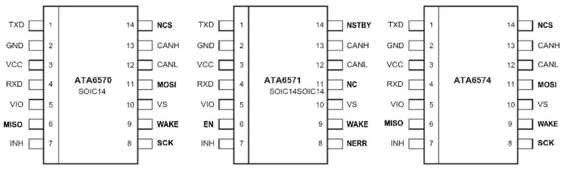
The ATA657X devices are available in a SOIC14 package as well as in a VDFN14 package, for space-saving applications. The ATAB657XA development board supports only SOIC14 packages. However, an adaptor board can be plugged in using the adaptor board-header, if a device in a VDFN package is used (the adaptor board is not within the scope of supply and services of this demo kit/board).
Figure 1. SOIC14 Pinning
Schematic and Layout for this board are available here: www.microchip.com/en-us/development-tool/EV16R67A.
Development Board Features
The development board for the ATA657X ICs supports the following features:
- All components necessary to put the ATA6570/ATA6574 or ATA6571 into operation are included
- Placeholders for some optional components for extended functions
- All pins are easily accessible
- Switching into Normal, Standby or Sleep mode via two jumpers (ATA6571)
- Push button included for creating a local wake-up after entering Sleep mode
• LEDs for operation indication - Ground coulter clip for easy probe connection while measuring with oscilloscope
- Connectors for direct plug-in with the C21-XPRO Xplained board (only ATA6570/ATA6574 with SPI)
What does the ATAB657XA Development Board Kit Contain?
The ATAB657XA Development Board kit includes:
• ATAB657XA Development Board
1. Hardware Description
The development board for the ATA657X is shipped with all the components needed to start developing a CAN node immediately. However, commands, data and status information are transferred to and from the ATA6570/ATA6574 via SPI. This is how the ATA6570/ATA6574 can be configured and operated.
Microchip offers an Xplained Pro board (ATSAMC21-XPRO Xplained board), which can be used to interface with the ATA657X GUI to operate and control the ATA6570/ATA6574. This Xplained Pro board must be ordered separately, as the ATAB657XA board comes as a stand-alone board. The ATA657X GUI can be downloaded directly from Microchip's web site: www.microchip.com/.
Figure 1-1. ATAB657XA Evaluation Board Overview
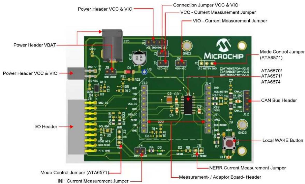
After correctly connecting an external 12V DC power supply (Power Header VBAT) to the power connector of the ATAB657X A board and connecting the Xplained Pro interface board to the PC via the USB cable, the kit is ready to use. To start working with the kit, execute the ata65xx.exe.
The ATA6570/ATA6574 IC starts in Standby mode, INH is active (if jumper J4 is set the LED D3 is ON) and the window watchdog is switched off for the ATA6570/ATA6574. A quick check to determine if everything is working properly can be done by executing the following:
CAN Communication Check:
- Click the Normal Mode button in the Operating mode section
- Click the Normal Mode button in the CAN transceiver section
- Set "TXD Pulsed"
- Choose 250 kHz as "Frequency" and press the Set button. A 250 kHz signal should be visible on the CANH and CANL pins, when you put oscilloscope probes on those pins.
Sleep/Wake-up Check:
- Select Falling edge or Rising edge in the Wake-up settings section
- Click the Sleep Mode button in the Operating mode section. Please keep in mind that at least one wake-up source should be selected prior to putting the ATA657X device into Sleep mode (to avoid dead lock). Otherwise, the Go to sleep command will be ignored and the device will switch to Standby mode.
- The INH will be switched off and, if the jumper J4 is set, the LED "D3" will be switched off.
- Press the local wake-up button (ATAB657X board) -> the LED D3 will be switched on (the ATA657X device switches from Sleep to Standby mode and the INH becomes active).
Watchdog Check:
- Press the STBY Mode button in the Operating mode section
- Select "Window mode"
- The LED D3 should be flashing – Watchdog resets at INH because the watchdog is not triggered
- Set 100 ms for the "Trigger period" in the Watchdog section
- Set "Trigger On"
- The LED D3 should be permanently on – Watchdog is working properly and no resets are generated at the INH pin
1.1 Power Supply
The ATAB657XA board can be powered by an external power source (4.5V to 28V) through the J15 connector or the 2-pin power header J9.
Additionally, a 5V external power source should be connected to the X5 connector (VCC), and the power source (2.8V to 5.5V) used to supply the selected microcontroller should be connected to the X5 connector (VIO) when working in stand-alone mode. When the ATAB657XA board is connected to a C21-XPRO Xplained Pro board, VIO and VCC will be delivered from the Xplained Pro board through the J10 power header. However, if it is necessary to have an external VIO and/or VCC power supply while an Xplained Pro board is connected to the ATAB657XA board, the resistors R19 and R20 should be removed.
1.1.1 Measuring the ATA657X Current Consumption
As part of an evaluation of the ATA657X device, it can be of interest to measure its current consumption. Because the device has different power supplies (VBAT, VCC and VIO), it is possible to measure the current consumption via separate jumpers. By replacing the jumper J6 by an ampere-meter, it is possible to determine the current consumption at VIO and, by replacing the jumper J7, it is possible to measure the current consumption at VCC.
1.2 Headers, Connectors and Jumpers
The following table describes the implementation of the relevant connectors, headers, and jumpers on the ATAB657XA evaluation board.
Table 1-1. Headers, Connectors and Jumpers
| Type Name Description | |
| Switch Jumper J1 | NSTBY-pin mode control jumper. The NSTBY pin, together with the EN pin, controls the operating mode of the device. Available only on the ATAB6571A board. |
| Switch Jumper J2 | EN-pin mode control jumper. The EN pin, together with the NSTBY pin, controls the operating mode of the device. Available only on the ATAB6571A board. |
| Jumper J3 | VIO to VCC jumper. If the VIO voltage is same as VCC (5V), this jumper can be set and only one supply can be applied at header J11. If VIO is different than VCC, this jumper should be removed. |
| ......continued | ||
| Type Name Description | ||
| Jumper J4 | When replacing the jumper J4 by an ampere-meter, it is possible to determine the current consumption at INH, or connect an external circuitry. When measuring the allover current consumption of the device, this jumper should be removed in order to disconnect the D3 LED from the INH pin. | |
| Jumper J5 | When replacing the jumper J5 by an ampere-meter, it is possible to determine the current consumption at NERR or to connect external circuitry. Or, when measuring the all-over current consumption of the device, this jumper should be removed in order to disconnect the D2 LED from the NERR pin. Available only on the ATAB6571A board. | |
| Jumper J6 | When replacing the jumper J6 by an ampere-meter, it is possible to determine the current consumption at VIO. | |
| Jumper J7 | When replacing the jumper J7 by an ampere-meter, it is possible to determine the current consumption at VCC. | |
| Connector J15 Main power supply connector - VBAT | ||
| Header J8 Interface header to C21-XPRO Xplained board | ||
| Header J10 | External supply power header - GND, VIO and VCC supplied from C21-XPRO Xplained board. | |
| Header J9 Optional main power supply connector - VBAT | ||
| Header J11 VCC and VIO power supply header | ||
| Header J12 CAN bus connection header | ||
1.3 Mechanical Buttons
There is one mechanical button on the ATAB657XA board. It is only mounted on the ATAB6570A and ATAB6571A boards, and it is used to generate a local wake-up. On the ATAB6572A variant, this button is not assembled.
1.4 LEDs
There are two LEDs available on the ATAB657XA board (LD1 and LD2) indicating activity on the INH pin and NERR pin, respectively. Via the jumpers J4 and J5, the LEDs can be deactivated if necessary (for example for current measurements, or if an external circuitry should be connected to the INH pin or to the NERR pin).
2. Mode Control
The ATA657X devices offer various operation modes.
The desired operating mode of the ATA6570/ATA6574 devices can be set via the SPI interface. With the dedicated GUI and the connected Xplained Pro interface board (C21-XPRO), configuring the ATA6570/ATA6574 devices can be easily done (for more information, see the Graphical User Interface (GUI) section).
The ATA6571 can be set into its different operating modes via the switch jumpers J1 and J2, which are connected with the NSTBY pin, and the EN pin, respectively. The following table shows the switch jumper setting and the corresponding selected mode.
Table 2-1. Mode Control Jumper Settings
| Mode J1 (NSTBY) Position J2 (EN) Position | |
| Sleep Mode In the middle In the middle | |
| Standby Mode Left (VIO) In the middle | |
| Standby Mode Right (GND) In the middle | |
| Standby Mode Right (GND) Up (GND) | |
| Sleep Mode Right (GND) In the middle | |
| Silent Mode Left (VIO) Up (GND) | |
| Normal Left (VIO) Down (VIO) |
Figure 2-1. ATAB6571A Evaluation Board Mode Change Jumpers

Normal Mode
A high level on the NSTBY pin and a high level on the EN pin select Normal mode. In this mode, the transceiver is able to transmit and receive data via the CANH and CANL bus lines. The output driver stage is active and drives data from the TXD input to the CAN bus. The differential receiver converts the analog data on the bus lines into digital data that is output to pin RXD. The bus biasing is set to VCC/2 and the undervoltage monitoring of VCC is active. Also the INH output is switched on.
The slope of the output signals on the bus lines is controlled and optimized in a way that guarantees the lowest possible electromagnetic emission (EME).
To switch the device in normal operating mode, set the NSTBY pin to high (jumper J1 set to the left side) and the EN pin to high (jumper J2 set to lower position).
The STBY and the EN pins each provide a pull-down current to GND, thus ensuring defined levels, if the pins are open.
Silent Mode
A high level on the NSTBY pin and a low level on the EN pin selects Silent mode. This receive-only mode can be used to test the connection of the bus medium. In Silent mode, the ATA6571 can still receive data from the bus, but the transmitter is disabled and therefore no data can be sent to the CAN bus. The bus pins are released to the recessive state (VCC/2) and the INH output remains active. All other IC functions, including the receiver, continue to operate as they do in Normal mode. Silent mode can be used to prevent a faulty CAN controller from disrupting all network communications.
Standby Mode
A low level on the NSTBY pin selects Standby mode. In this mode, the transceiver is not able to transmit or correctly receive data via the bus lines. The transmitter and the Normal-mode receiver are switched off to reduce current consumption, and only a low-power differential receiver monitors the bus line for a valid wake-up signal. If a dominant state longer than twake is received, the RXD switches to low to signal a wake-up request.
In Standby mode, the bus lines are biased to ground to reduce current consumption to a minimum. The low-power differential receiver monitors the bus lines for a valid wake-up signal. When the RXD pin switches to low to signal a wake-up request, a transition to Normal mode is not triggered until the STBY pin is forced back to low by the microcontroller.
In the event the NSIL input pin is set to low in Standby mode, the internal pull-up resistor causes an additional quiescent current from VIO to GND. Microchip therefore recommends setting the NSIL to high in Standby mode.
Sleep Mode
In Sleep mode the current into the VS pin is reduced to a minimum. The behavior of the transceiver is the same as in Standby mode, but the INH output is switched off.
3. Graphical User Interface (GUI)
Figure 3-1. ATA6570/ATA6574 Graphical User Interface

Note: The root directory of the GUI contains installers for the Visual C# runtime from Microsoft * and for the Microchip USB drivers. Both are necessary to run the GUI and must be run before the GUI is launched. vc_redist.x86.exe should be installed for x86/x64 based systems. For the USB driver, the correct installer should be chosen depending on the host computer.
3.1 Features
- Configuration of functions
- Operating mode
- CAN Transceiver mode
- Watchdog
- System events
- Wake-up settings
- CAN-PN settings
- General-purpose memory
- Status bits
- Lock Control
- Direct read/write to all registers
- Configuration for Xplained Pro
- Watchdog trigger
- CAN TXD pin static/pulsed/data
- SPI commands
The ATA65xx GUI is a PC software application that graphically displays the configuration of an ATA657X device received through the PC's USB connection. The received data is shown in different tabs.
3.2 Maintab
This tab gives access to most of the functionality from a feature perspective. The device can be configured without accessing the registers directly. Register accesses (read and write) will happen in the background and will be printed to the SPI log window.
This tab is not refreshed periodically. Instead, relevant parts are refreshed when performing an action. For example, when configuring the operating mode, the mode is read back and updated accordingly. There are two ways to refresh the complete tab:
- Switch from a different tab
- Select a different SAMC21 Xplained Pro board in the Serial Selection section and press Refresh.
Both methods will refresh the entire Maintab.
3.2.1 Serial Selection
The GUI supports connecting to multiple SAMC21 Xplained Pro boards, hence it is necessary to select which one to send the command to. In the drop-down menu, all boards with a suitable firmware are shown. Commands are sent to the currently selected one. The board can be identified by the serial number that is also shown in this window. This serial number is printed on a sticker on the bottom of the PCB. To help identify the board, the LED0 close to the SW0 can be toggled by the GUI.
3.2.2 Operating Mode
The operating mode of the device can be chosen in this section. The available modes are Standby, Normal and Sleep modes, as described in the data sheet. Additionally, the state of the INH pin is continuously monitored and shown in a check box. The switch to Normal and Standby mode can
always be executed by issuing the corresponding write to the DCMR register. To enter Sleep mode, certain conditions must be fulfilled, which are described in the data sheet. The GUI checks for these conditions and, if they are not fulfilled, logs an error in the SPI log window. The mode will remain as before. A write attempt to DCMR will not happen.
3.2.3 CAN Transceiver
In this section, the transceiver part can be configured. For the CAN Transceiver, the following modes are accessible:
- Standby mode
- Normal mode
- Normal mode with undervoltage detection active
- Silent mode.
Note: To use the transceiver, the device operating mode has to be Normal mode. This mode can be changed as described in Operating Mode.
In this section, it is also possible to control an output of the SAMC21 connected to the TXD input. The available options are:
- TXD pulsed - this will pulse the TXD with a 50% duty cycle
- TXD static low
- TXD static high
- TXD tristate - in this case, the internal pull-up on the ATA657X will pull the pin high.
When the pulse option is selected, the nearest possible value for the frequency will be selected and the Freq. cell will be updated accordingly.
3.2.4 Watchdog
In this section, the watchdog can be configured. The available modes are:
• "Off"
- "Window mode"
- "Time-Out mode".
Additionally, all the configuration bits for the watchdog can be controlled.
The following bits can be set/cleared:
- "Active in Sleep mode" - sets/clears the WDSLP bit in the WDCR1 register
- "Long startup window" - sets/clears the WDLW bit in the WDCR1 register
- "Active Discharge" - sets/clears the ADCH bit in the WDCR1 register.
"Watchdog period" and "Reset pulse length" control the settings in WDCR1 and WDCR2.
Note: In order to avoid unwanted configuration of the window watchdog (WWD), the ATA6570/ATA6574 only allows users to configure the WWD (write access to WDCR1 register and WDCR2) when the device is in Standby mode. For more information, please see the data sheet.
An appropriate trigger setup should be made that configures the SAMC21 Xplained Pro to generate an SPI trigger command with the configured frequency. Activating the trigger will first update the frequency on the SAMC21 Xplained Pro and then activate the continuous triggering.
3.2.5 System Events
This section allows the user to enable/disable the capturing of all events distributed across the different registers. The current status is indicated next to the button that toggles the status. The following bits can be configured:
• BOUTE - Bus dominant time-out timer
• BSCE - Bus short circuit event
- SPIFE - SPI failure event
• BSE - CAN bus status detection
• TRXFE - TXD failure status
• CWUE - CAN wake-up event
- OTPWE - Overtemperature event.
The displayed status is not a live-view and only updates when the corresponding button is pressed or the complete tab is updated, as described in the Maintab section.
3.2.6 Wake-up Settings
In this section, all wake-up sources supported by the ATA657X device can be activated. For the Local wake-up on the Wake pin, falling, rising or both edges can be configured as a valid wake-up source. For the Remote wake-up, either wake-up pattern, wake-up frame or none have to be configured. If "Wake-Up Frame" is selected, the frame must be configured as described in section CAN PN Settings. The SPI wake-up button will wake up the device by setting the device into Standby mode. The four check boxes are updated when a full refresh on the Maintab tab is performed.
3.2.7 CAN PN Settings
This section allows the user to configure the CAN-PN functionality available in the ATA657X. The wake-up frame can be configured with either an STD identifier or an extended one, and, if necessary, a data byte mask can be activated, as well.
Notes:
- The data bytes are a mask of bits expected to be 1, i.e., a data byte of 0xAA on the bus will generate a wake-up for devices configured for 0x01, 0x0A and 0xAA and others where all bits selected in the mask are fulfilled.
- The configuration for the CAN PN only becomes valid and active after the PNCFOK flag has been set. This can be done by pressing the "Set PNCFOK" button in this section.
3.2.8 General Purpose Memory
This section gives access to the four bytes of general purpose memory available on the ATA657X (available at addresses 0x6-0x9). The bytes read/written are selected with the check boxes. The displayed values are not a live-view but only update when the corresponding button is pressed or the complete tab is updated as described in the Maintab section.
3.2.9 Status Bits
This section gives an overview of all status bits of the device. The display is not updated continuously but must be refreshed manually by clicking the Read Status bits button.
Bits can not be manipulated individually, but it is possible to clear all status-bits that are writable at once. The following bits are cleared when clicking the Clear Status bits button:
- "BOUTS" - Bus dominant timeout status
- "BS" - Bus silence
• "BSCS" - Bus short circuit - "CACC" - Corrupted write access to watchdog configuration registers
- "CWUS" - CAN wake-up status
• "ETRIG" - Early watchdog trigger -
"ILLCONF" - Watchdog configuration was written while the device is not in Standby mode
-
"LWUFS" - Local wake-up falling edge detected
- "LWURS" - Local wake-up rising edge detected
- "OF" - Watchdog overflow
- "OFSLP" - Watchdog overflow in Sleep mode
- "OTPW" - Over-temperature pre-warning
- "PNEFD" - Partial networking frame detection status
- "PWRONS" - Power-on Reset
- "SPIFS" - SPI failure status
- "TRXF" - Transceiver failure.
A list of all status-bits and their descriptions can be found in the data sheets www.microchip.com/wwwproducts/en/ATA6570, www.microchip.com/wwwproducts/en/ATA6574.
3.2.10 Lock Control
In this section, it is possible to control the bits locking specific parts of the device memories. All seven lock bits can be configured. The configuration is only written/read when pressing the write/read button. Ticking the check boxes will not update the value on the ATA657X. The displayed status is not a live-view but only updates when the corresponding button is pressed or the complete tab is updated, as described in section Maintab.
3.2.11 SPI Log Window
In this section, all SPI communication with the ATA657X will be logged, and possible errors are displayed. The log can be cleared by pressing the Clear SPI log button below it. The log entry will be made as soon as an action in the GUI is performed. If the command was accepted by the ATA657X, it is not actually checked. As more data is written in the log file, the GUI navigation speed might be affected. In such cases, try clearing the log.
3.3 Registers
This tab allows the user to manipulate the registers directly. Each column shows the name of the register, the address, the last read value and gives the option to read from the register or write to it.
Figure 3-2. Registers
![graph TD A["addressvalue"] --> B["DMCR"] A --> C["0x01"] C --> D["(hex)"] D --> E["Read"] D --> F["Write"]](/content/2026/05/1016162/images/51c61ddaa68aafb6e748372d64b2012f57f042706adc72930207c65b68acfd15.jpg)
It is also possible to read all registers at once. When writing registers, it is possible to automatically verify the value afterward. This is selectable with the check box "Verify after write". Until a value is verified, it will be shown in a red font.
Note: The displayed values are not a live-view but only updates when the corresponding button is pressed or the complete tab is updated by a tab-switch.
3.4 SPI
This tab allows to send SPI commands to the ATA657X device directly. This can be useful for writing multiple registers at the same time or for debugging purposes. To read an address, a valid hex value must be entered in the Address (hex) field.
Figure 3-3. SPI

Note: The data is sent out starting from the lowest significant byte. The order in which the bytes are sent is from right to left. Writing address 0x06 and data 0xAA55 will write 0x55 to 0x06 and 0xAA to 0x07.
3.5 CAN
This tab allows some very limited sending of CAN messages for testing. Only "singleshot" messages are supported.
Figure 3-4. CAN
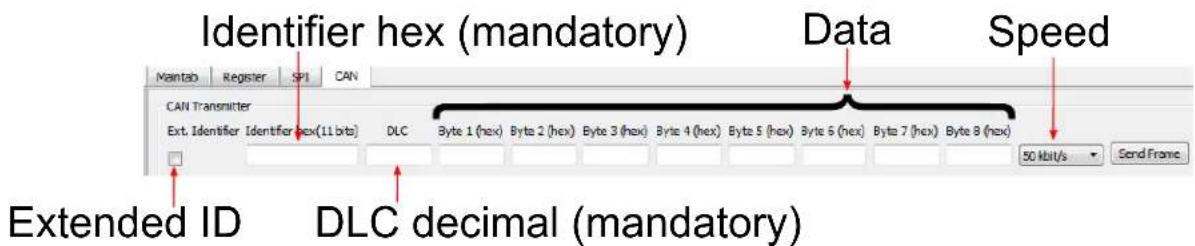
To initiate a transmission, the identifier, the DLC, and at least the number of bytes specified in the DLC must be given. After clicking send frame, the frame will be sent one time, if the configuration is valid. It is not possible to receive CAN data.
4. Test Setups and Measurements
4.1 Various Measurements
The required components on the basic application board can be found below. A two- or better four-channel oscilloscope is sufficient to measure the timing characteristics of the ATA657X. The transmit data signal TXD can be generated by any signal generator that is capable of delivering a rectangular or pulse signal with 3.3V to 5V amplitude, referenced to ground or directly from the GUI. The temporal relation of TXD, RXD and the CANH, CANL signals, for example, can be examined.
Figure 4-1. Test Circuit

The footprint for an optional common-mode choke is implemented on the ATAB657XA Development Board. This common-mode choke is replaced by two 0Ω resistors by default.
Instead of a one-resistor termination, it is highly recommended to use split termination, which is assembled by default. EMC measurements have shown that split termination is able to significantly improve the signal symmetry between CANH and CANL, thus reducing emissions. Basically, the termination is split into two resistors of equal value (per default mounted: R2 = R3 = 62Ω ) and a capacitor ( C1 ) to GND at the center tap, which represents one of the two usual bus end terminations. The special characteristic of this approach is that the common-mode signal, available at the center tap of the two resistors, is terminated to ground via the capacitor C1 . The recommended value for this capacitor C1 is in the range of 4.7 nF to 47 nF (4.7 nF mounted per default). As the symmetry of the two signal lines is crucial for the emission performance of the system, the matching tolerance of the two termination resistors R1 and R2 should be as low as possible (< 1% is desirable).
Timing Measurements
Additionally placeholders are implemented on the board for timing measurements ( R1 , C6 and C4 ).
Figure 4-2. Components to be Removed (Red) or Replaced (Green) for the Timing Measurement Setup

If a function generator is connected to the TXD header, it can be adjusted to output a rectangular signal up to a frequency corresponding to the maximum data rate of the final application. Please ensure that its output signal levels are in the appropriate range, particularly that no negative voltage occurs. Of course, the function generator can be replaced by a dedicated data generator in order to form a better approach to the desired application or use the Xplained Pro board. The high-impedance inputs of the oscilloscope can be connected directly; however, it is advantageous to use probes, so that the signals are not noticeably affected by the capacitance of the coaxial cable.
Figure 4-3. Communication Signals of the ATA657X

4.2 Measurement Hints
4.2.1 Passive Behavior
In up-to-date, in-vehicle networks, partial networking is widely implemented. In these applications, some transceivers can become unpowered (e.g., Clamp-15 nodes), while other transceivers are continuously supplied (e.g., Clamp-30 nodes). In such networks, the ATA657X is favored for those applications, which are partly unpowered, because of its excellent passive behavior to the bus when the VCC supply is switched off. In addition, the ATA657X is protected against reverse currents via the TXD, RXD and STB pins. There will be no backward current via those pins if the accompanying microcontroller is still supplied.
4.2.2 Optional Circuitry at CANH and CANL
The EMC performance of the ATA657X has been optimized for use of the CAN termination without a common-mode choke. The excellent output stage symmetry allows usage without chokes. If, however, the system performance is still not sufficient, there is the option to use additional measures like common-mode chokes (a footprint for a common-mode choke is available on the ATAB657XA board), capacitors and ESD clamping diodes. Please note that if any critical measurements on EMI (electromagnetic interference) performance, like electromagnetic immunity or electromagnetic emission, shall be taken, it is recommended to use a dedicated board with highly symmetrical layout for the bus lines and ground-vias at each connection to the ground plane. For investigations on complete links, like bit error measurements, a test board with at least two transceivers is required.
4.2.2.1 Common-Mode Choke
A common-mode choke provides high impedance for common-mode signals and low impedance for differential signals. Due to this, common-mode signals produced by RF noise and/or by nonperfect transceiver driver symmetry get effectively reduced while passing the choke. In fact, a common-mode choke helps reduce emission and improve immunity against common-mode disturbances. Older transceiver devices usually needed a common-mode choke to fulfill the stringent emission
and immunity requirements of the automotive industry, when using unshielded twisted-pair cable. The ATA657X has the potential to build in-vehicle bus systems without chokes. Whether a choke is needed or not ultimately depends on the specific system implementation, such as the wiring harness and the symmetry of the two bus lines (matching tolerances of resistors and capacitors). In addition to the RF noise reduction, the stray inductance (noncoupled portion of inductance) may establish a resonant circuit together with pin capacitance. This can result in unwanted oscillations between the bus pins and the choke, for both differential and common-mode signals, and in extra emissions around the resonant frequency. To avoid such oscillations, it is highly recommended to use only chokes with a stray inductance lower than 500 nH. Bifilar wound chokes typically show an even lower stray inductance. The choke shall be placed nearest to the transceiver bus pins.
The use of common-mode chokes in CAN systems may cause extremely high transient voltages at the bus pins of the transceiver. These transients are generated by the change in current through the inductance of the common-mode chokes if the CAN bus is shorted to DC voltages. The actual transients that may be generated are highly dependent on the common-mode choke type and value, and also depend on the CAN system architecture, termination, components, and location and the severity of the short circuit.
For systems where common-mode chokes are required, care should be used in the choice of the common-mode choke and the system circuit to avoid the introduction of severe transients during DC short-circuit conditions on the bus.
The best methods to avoid transients generated from common-mode chokes during CAN bus line shorts to DC voltages are:
- Remove common-mode chokes from systems, where applicable.
- Move transient suppression circuits between the common-mode choke and the CAN bus pins on the transceiver.
- Choose a common-mode choke type and value, and a CAN termination scheme to minimize transients.
4.2.2.2 Capacitors
Matching capacitors (in pairs) at CANH and CANL to GND are frequently used to enhance immunity against electromagnetic interferences. Along with the impedance of corresponding noise sources (RF), capacitors at CANH and CANL to GND form an RC low-pass filter. Regarding immunity, the capacitor value should be as large as possible to achieve a low corner frequency. The overall capacitive load and impedance of the output stage establish an RC low-pass filter for the data signals. The associated corner frequency must be well above the data transmission frequency. This results in a limit for the capacitor value depending on the number of nodes and the data transmission frequency. Notice that capacitors increase the signal loop delay due to reducing rise and fall times. Due to that, bit timing requirements, especially at 1 Mbit/s, call for a value of lower than 100 pF (see also SAE J2284 and ISO 11898). At a bit rate of 125 Kbit/s, the capacitor value should not exceed 470 pF. Typically, the capacitors are placed between the common-mode choke (if applied at all) and the ESD clamping diodes.
4.2.2.3 ESD Protection
The ATA657X is designed to withstand ESD pulses of up to 8 kV according to the human body model at the CANH and CANL bus pins, and thus typically does not need further external protection methods. Nevertheless, if much higher protection is required, external clamping devices can be applied to the CANH and CANL lines.
Care must be taken when selecting the right protection devices. The transient protectors must be fast enough to clamp the transient voltages. In addition, their capacitance must be considered. If the capacitance is too high, it can work together with the choke's inductance and cause ringing on the bus signals. Although this ringing does not corrupt the CAN signals, it may show up as electromagnetic emission at higher frequencies.
5. Revision History
Revision C (November 2024)
Adjusted for latest HW revision.
Revision B (July 2018)
Deleted Product Information Section
Revision A (February 2018)
Original release of the document
Microchip Information
Trademarks
The “Microchip” name and logo, the “M” logo, and other names, logos, and brands are registered and unregistered trademarks of Microchip Technology Incorporated or its affiliates and/or subsidiaries in the United States and/or other countries (“Microchip Trademarks”). Information regarding Microchip Trademarks can be found at https://www.microchip.com/en-us/about/legal-information/microchip-trademarks.
ISBN: 979-8-3371-0121-7
Legal Notice
This publication and the information herein may be used only with Microchip products, including to design, test, and integrate Microchip products with your application. Use of this information in any other manner violates these terms. Information regarding device applications is provided only for your convenience and may be superseded by updates. It is your responsibility to ensure that your application meets with your specifications. Contact your local Microchip sales office for additional support or, obtain additional support at www.microchip.com/en-us/support/design-help/client-support-services.
THIS INFORMATION IS PROVIDED BY MICROCHIP "AS IS". MICROCHIP MAKES NO REPRESENTATIONS OR WARRANTIES OF ANY KIND WHETHER EXPRESS OR IMPLIED, WRITTEN OR ORAL, STATUTORY OR OTHERWISE, RELATED TO THE INFORMATION INCLUDING BUT NOT LIMITED TO ANY IMPLIED WARRANTIES OF NON-INFRINGEMENT, MERCHANTABILITY, AND FITNESS FOR A PARTICULAR PURPOSE, OR WARRANTIES RELATED TO ITS CONDITION, QUALITY, OR PERFORMANCE.
IN NO EVENT WILL MICROCHIP BE LIABLE FOR ANY INDIRECT, SPECIAL, PUNITIVE, INCIDENTAL, OR CONSEQUENTIAL LOSS, DAMAGE, COST, OR EXPENSE OF ANY KIND WHATSOEVER RELATED TO THE INFORMATION OR ITS USE, HOWEVER CAUSED, EVEN IF MICROCHIP HAS BEEN ADVISED OF THE POSSIBILITY OR THE DAMAGES ARE FORESEEABLE. TO THE FULLEST EXTENT ALLOWED BY LAW, MICROCHIP'S TOTAL LIABILITY ON ALL CLAIMS IN ANY WAY RELATED TO THE INFORMATION OR ITS USE WILL NOT EXCEED THE AMOUNT OF FEES, IF ANY, THAT YOU HAVE PAID DIRECTLY TO MICROCHIP FOR THE INFORMATION.
Use of Microchip devices in life support and/or safety applications is entirely at the buyer's risk, and the buyer agrees to defend, indemnify and hold harmless Microchip from any and all damages, claims, suits, or expenses resulting from such use. No licenses are conveyed, implicitly or otherwise, under any Microchip intellectual property rights unless otherwise stated.
Microchip Devices Code Protection Feature
Note the following details of the code protection feature on Microchip products:
- Microchip products meet the specifications contained in their particular Microchip Data Sheet.
- Microchip believes that its family of products is secure when used in the intended manner, within operating specifications, and under normal conditions.
- Microchip values and aggressively protects its intellectual property rights. Attempts to breach the code protection features of Microchip products are strictly prohibited and may violate the Digital Millennium Copyright Act.
- Neither Microchip nor any other semiconductor manufacturer can guarantee the security of its code. Code protection does not mean that we are guaranteeing the product is "unbreakable". Code protection is constantly evolving. Microchip is committed to continuously improving the code protection features of our products.


- ATA6570/ATA6571/ATA6574 DEVELOPMENT BOARD USER'S GUIDE
- INTRODUCTION
- DEVELOPMENT BOARD FEATURES
- WHAT DOES THE ATAB657XA DEVELOPMENT BOARD KIT CONTAIN
- HARDWARE DESCRIPTION
- CAN COMMUNICATION CHECK
- WATCHDOG CHECK
- 1.1 POWER SUPPLY
- 1.1.1 MEASURING THE ATA657X CURRENT CONSUMPTION
- 1.2 HEADERS, CONNECTORS AND JUMPERS
- 1.3 MECHANICAL BUTTONS
- 1.4 LEDS
- MODE CONTROL
- NORMAL MODE
- SILENT MODE
- STANDBY MODE
- SLEEP MODE
- GRAPHICAL USER INTERFACE (GUI)
- 3.1 FEATURES
- 3.2 MAINTAB
- 3.2.1 SERIAL SELECTION
- 3.2.2 OPERATING MODE
- 3.2.3 CAN TRANSCEIVER
- 3.2.4 WATCHDOG
- 3.2.5 SYSTEM EVENTS
- 3.2.6 WAKE-UP SETTINGS
- 3.2.7 CAN PN SETTINGS
- NOTES
- 3.2.8 GENERAL PURPOSE MEMORY
- 3.2.9 STATUS BITS
- 3.2.10 LOCK CONTROL
- 3.2.11 SPI LOG WINDOW
- 3.3 REGISTERS
- 3.4 SPI
- 3.5 CAN
- TEST SETUPS AND MEASUREMENTS
- 4.1 VARIOUS MEASUREMENTS
- TIMING MEASUREMENTS
- 4.2 MEASUREMENT HINTS
- 4.2.1 PASSIVE BEHAVIOR
- 4.2.2 OPTIONAL CIRCUITRY AT CANH AND CANL
- 4.2.2.1 COMMON-MODE CHOKE
- 4.2.2.2 CAPACITORS
- 4.2.2.3 ESD PROTECTION
- REVISION HISTORY
- MICROCHIP INFORMATION
- TRADEMARKS
- LEGAL NOTICE
- MICROCHIP DEVICES CODE PROTECTION FEATURE
Brand : Microchip
Model : ATA6574
Category : Carte de développement électronique