SY56216R - Electronic component Microchip - Free user manual and instructions
Find the device manual for free SY56216R Microchip in PDF.

User questions about SY56216R Microchip
0 question about this device. Answer the ones you know or ask your own.
Ask a new question about this device
Download the instructions for your Electronic component in PDF format for free! Find your manual SY56216R - Microchip and take your electronic device back in hand. On this page are published all the documents necessary for the use of your device. SY56216R by Microchip.
USER MANUAL SY56216R Microchip
The SY56216R is a fully-differential, low-voltage 1.2V/1.8V/2.5V CML Dual Channel Buffer with input equalization. The SY56216R can process clock signals as fast as 4.5GHz or data patterns up to 6.4Gbps.
The differential input includes Micrel's unique, 3-pin input termination architecture that interfaces to CML differential signals, without any level-shifting or termination resistor networks in the signal path. The differential input can also accept AC-coupled LVPECL and LVDS signals. Input voltages as small as 200mV (400mV pp ) are applied before the 9", 18" or 27" FR4 transmission line. For AC-coupled input interface applications, an internal voltage reference is provided to bias the V T pin. The outputs are CML, with extremely fast rise/fall times guaranteed to be less than 80ps.
The SY56216R operates from a 2.5V ±5% core supply and a 1.2V, 1.8V or 2.5V ±5% output supply and is guaranteed over the full industrial temperature range ( -40^ to +85^ ). The SY56216R is part of Micrel's high-speed, Precision Edge ^® product line.
Datasheets and support documentation can be found on Micrel's web site at: www.micrel.com.
Functional Block Diagram

text_image
IN0 50Ω V70 50Ω /IN0 EQ0 Equalization Q0 /Q0 IN1 50Ω VT1 50Ω /IN1 EQ1 Equalization Q1 /Q1Precision Edge is a registered trademarks of Micrel, Inc.

Features
• 1.2V/1.8V/2.5V CML Dal Channel Buffer
• Guaranteed AC performance over temperature and voltage:
- DC-to > 6.4Gbps Data throughput
- DC-to > 4.5GHz Clock throughput
- <280ps propagation delay (IN-to-Q)
- <20ps within-device skew
- <80ps rise/fall times
• High-speed CML outputs
- 2.5V ±5% V_CC , 1.2/1.8V/2.5V ±5% V_CCO power supply operation
- Industrial temperature range: -40^ to +85^
• Available in 16-pin (3mm x 3mm) QFN package
Applications
• Data Distribution:
• SONET clock and data distribution
• Fiber Channel clock and data distribution
• Gigabit Ethernet clock and data distribution
Markets
- Storage
- ATE
• Test and measurement
• Enterprise networking equipment
• High-end servers
• Metro area network equipment
Ordering Information ^(1)
| Part Number Package Type Operating Range Package Marking Lead Finish | |
| SY56216RMG QFN-16 Industrial R216 with Pb-Free bar-line indicator NiPdAu / Pb-Free | |
| SY56216RMGTR(2) QFN-16 Industrial R216 with Pb-Free bar-line indicator NiPdAu / Pb-Free |
Notes:
1. Contact factory for die availability. Dice are guaranteed at T A = 25°C, DC Electricals only.
2. Tape and Reel.
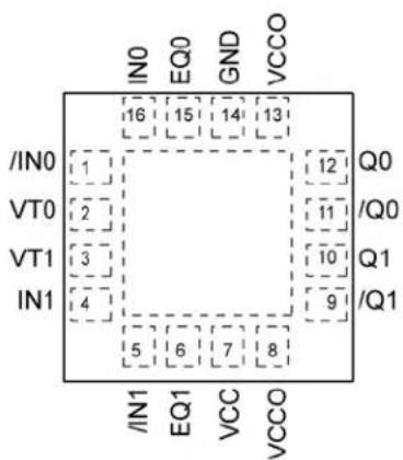
Pin Configuration
text_image
/IN0 VT0 VT1 IN1 IN0 EQ0 GND VCCO 16 15 14 13 12 Q0 2 11 /Q0 3 10 Q1 4 9 /Q1 5 6 7 8 IN1 EQ1 VCC VCCO16-Pin QFN
Truth Table
| EQ Setting | EQUALIZATION FR4 6 mil Stripline |
| LOW | 9 |
| FLOAT | 18" |
| HIGH | 27" |
Pin Description
| Pin Number | Pin Name Pin Function | |
| 16,14,5 | IN0, /IN0IN1, /IN1 | Differential Inputs: Signals as small as 200mVpk (400mVPP) applied to the input of 9, 18 or 27 inches 6 mil FR4 stripline transmission line are then terminated the differential input. Each input pin internally terminates with 50Ω to the VT pin. |
| 2,3 | VT0, VT1 | Input Termination Center-Tap: Each side of the differential input pair terminates to a VT pin. This pin provides a center-tap to a termination network for maximum interface flexibility. An internal high-impedance resistor divider biases VT to allow input AC coupling. For AC coupling, bypass VT with 0.01μF low-ESR capacitor to VCC. See “Interface Applications” subsection and Figure 2a. |
| 15,6 EQ0 | EQ1 Three level | inputs for equalization control. Low, Float, High |
| 7 | VCC | Positive Power Supply: Bypass with 0.1μF//0.01μF low-ESR capacitors as close to the VCC pins as possible. Supplies input and core circuitry. |
| 8,13 | VCCO | Output Supply: Bypass with 0.1μF//0.01μF low-ESR capacitors as close to the VCCO pins as possible. Supplies the output buffers. |
| 14 | GND, Exposed pad | Ground: Exposed pad must be connected to a ground plane that is the same potential as the ground pins. |
| 12,1110,9 | Q0, /Q0Q1, /Q1 | CML Differential Output Pairs: Differential buffered copy of the input signal. The output swing is typically 390mV. See “Interface Applications” subsection for termination information. |
Absolute Maximum Ratings ^(1)
Supply Voltage ( V_cc ) -0.5V to +3.0V
Supply Voltage ( V_CCO ) -0.5V to +3.0V
V_cc - V_cco <1.8V
V_CCO-V_CC <0.5V
Input Voltage ( V_IN ) -0.5V to V_CC
CML Output Voltage ( V_OUT ).... 0.6V to 3.0V
Current ( V_T )
Source or sink on VT pin ....±100mA
Input Current
Source or sink Current on (IN, /IN) ....±50mA
Maximum Operating Junction Temperature..... 125°C
Lead Temperature (soldering, 20sec.) 260°C
Storage Temperature ( T_s ) -65^ to +150^
Operating Ratings ^(2)
Supply Voltage ( V_cc ).... 2.375V to 2.625V
(V_CCO) 1.14V to 2.625V
Ambient Temperature ( T_A ) ..... -40°C to +85°C
Package Thermal Resistance ^(3) QFN
Still-air ( _JA ) 75°C/W
Junction-to-board ( _JB )....33°C/W
DC Electrical Characteristics ^(5)
T_A = -40^ to +85^ , unless otherwise stated.
| Symbol | Parameter Condition | Min. Typ. Max. | Units | |||
| V_CC | Power Supply Voltage Range | V_CC | 2.375 | 2.5 | 2.625 | V |
| V_CCO | 1.14 | 1.2 | 1.26 | |||
| V_CCO | 1.7 | 1.8 | 1.9 | |||
| V_CCO | 2.375 | 2.5 | 2.625 | |||
| I_CC Power | Supply Current Maximum V _CC . | 72 | 105 | mA | ||
| I_CCO | Power Supply Current | No Load. Maximum V_CCO . | 32 | 42 | mA | |
| R_IN | Input Resistance (IN-to- V_T , /IN-to- V_T ) | 45 | 50 | 55 | Ω | |
| R_DIFF\_IN | Differential Input Resistance (IN-to-/IN) | 90 | 100 | 110 | Ω | |
| V_IH | Input HIGH Voltage (IN, /IN) | IN, /IN | 1.42 | _CC | V V | |
| V_IL Input LOW Voltage (IN, /IN) | IN, /IN1.22V=1.7-0.475 | 1.22 | V_IH-0.2 | V | ||
| V_IN | Input Voltage Swing (IN, /IN) | See Figure 3a, applied to input of transmission line. | 0.2 | 1.0 | V | |
| V_DIFF\_IN | Differential Input Voltage Swing (|IN - /IN|) | See Figure 3b, applied to input of transmission line. | 0.4 | 2.0 | V | |
| V_T\_IN | Voltage from Input to V_T | 1.28 | ||||
Notes:
- Permanent device damage may occur if absolute maximum ratings are exceeded. This is a stress rating only and functional operation is not implied at conditions other than those detailed in the operational sections of this data sheet. Exposure to absolute maximum ratings conditions for extended periods may affect device reliability.
- The data sheet limits are not guaranteed if the device is operated beyond the operating ratings.
- Package thermal resistance assumes exposed pad is soldered (or equivalent) to the device's most negative potential on the PCB. _JB and _JA values are determined for a 4-layer board in still-air number, unless otherwise stated.
- Due to the limited drive capability, use for input of the same package only.
- The circuit is designed to meet the DC specifications shown in the above table after thermal equilibrium has been established.
CML Outputs DC Electrical Characteristics ^(6)
V_CCO = 1.14V to 1.26V, R_L = 50 to V_CCO.
V_CCO = 1.7V to 1.9V , 2.375V to 2.625V , R_L = 50 to V_CCO or 100 across the outputs,
V_CC = 2.375V to 2.625V, T_A = -40^ to +85^, unless otherwise stated.
| Symbol | Parameter Condition | Min. | Typ. | Max. | Units | ||
| V_OH Output | HIGH Voltage R | _L=50 to V_CCO | V_CC-0.020 V | _cc-0.010 | V_CC | V | |
| V_OUT Output | Voltage Swing See Figure 3a 300 | 390 | 475 | mV | |||
| V_DIFF\_OUT | Differential Output Voltage Swing | See Figure 3b | 600 | 780 | 950 | mV | |
| R_OUT | Output Source Impedance | 45 | 50 | 55 | |||
Three Level EQ Input DC Electrical Characteristics ^(6)
V_CC = 2.375V to 2.625V, T_A = -40^ to +85^, unless otherwise stated.
| Symbol | Parameter | Condition | Min. | Typ. | Max. | Units |
| V_IH | Input HIGH Voltage | V_CC - 0.3 | V | |||
| V_IL | Input LOW Voltage | 0 | V_EE+0.3 | V | ||
| I_IH | Input HIGH Current | VIH = V_CC | 400 | uA | ||
| I_IL | Input LOW Current | VIL = GND | -450 | uA |
Note:
- The circuit is designed to meet the DC specifications shown in the above table after thermal equilibrium has been established.
AC Electrical Characteristics
V_CCO = 1.14V to 1.26V, R_L = 50 to V_CCO.
V_CCO = 1.7V to 1.9V , 2.375V to 2.625V , R_L = 50 to V_CCO or 100 across the outputs,
V_CC = 2.375V to 2.625V, T_A = -40^ to +85^, unless otherwise stated.
| Symbol | Parameter | Condition | Min. | Typ. | Max. | Units | |
| f_MAX | Maximum Frequency | NRZ Data | 6.4 | Gbps | |||
| V_OUT > 200mV | Clock | 4.5 | GHz | ||||
| t_PD | Propagation Delay | IN-to-Q, Figure 1 | 100 | 180 | 280 | ps | |
| t_Skew | Within Device Skew | Note 7 | 4 | 20 | ps | ||
| Part-to-Part Skew | Note 8 | 100 | ps | ||||
| t_Jitter | Random Jitter | Note 9 | 1 | ps_RMS | |||
| Crosstalk Induced Jitter (Adjacent Channel) | Note 10 | 0.7 | ps_PP | ||||
| t_Rt_F | Output Rise/Fall Times(20% to 80%) | At full output swing. | 20 | 50 | 80 | ps | |
Notes:
- Within device skew is the difference in t_PD between the two channels under identical input transition, temperature and power supply.
- Part-to-part skew is defined for two parts with identical power supply voltages at the same temperature and no skew at the edges at the respective inputs.
- Random jitter is measured with a K28.7 pattern, measured at ≤ f_MAX .
- Crosstalk induced jitter is defined as the added jitter that results from signals applied to the adjacent channel. It is measured at the output while applying a similar, differential clock frequency that is asynchronous with respect to each other at the adjacent input.
Interface Applications
For Input Interface Applications see Figures 4a through 4e. For CML Output Termination see Figures 5a through 5d
CML Output Termination with VCCO 1.2V
For VCCO of 1.2V, Figure 5a, terminate the output with 50Ω-to-1.2V, DC coupled, not 100Ω differentially across the outputs.
If AC-coupling is used, Figure 5d, terminate into 50Ω-to-1.2V before the coupling capacitor and then connect to a high value resistor to a reference voltage.
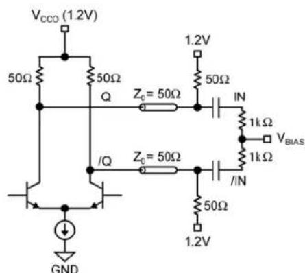
Do not AC couple with internally terminated receiver. For example, 50Ω ANY-IN input. AC-coupling will offset the output voltage by 200mV and this offset voltage will be too low for proper driver operation. Any unused output pair needs to be terminated when VCCO is 1.2V, do not leave floating.
CML Output Termination with 1.8V/2.5V Vcc0
For VCCO of 1.8V or 2.5V, Figure 5a and Figure 5b, terminate with either 50 -to- V_CCO or 100 differentially across the outputs. AC- or DC-coupling is fine. See Figure 5c for AC-coupling.
Input AC-Coupling
The SY56216R input can accept AC-coupling from any driver. Bypass VT with a 0.1μF low ESR capacitor to VCC as shown in Figures 4b and 4c. VT has an internal high impedance resistor divider as shown in Figure 2a, to provide a bias voltage for AC-coupling.
Input Termination
From 1.8V CML driver. Terminate with VT tied to 1.8V. Do not terminate 100 ohms differentially.
From 2.5V CML driver. Terminate with either VT tied to 2.5V or 100 ohms differentially.
The input cannot be DC-coupled from a 1.2V CML driver.
Timing Diagrams

text_image
/IN IN /Q Q tpdFigure 1. Propagation Delay
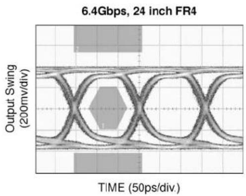
Typical Characteristics
V_CC = 2.5, V_CCO = 1.2V, GND = 0V, V_IN = 160mV, R_L = 50 to 1.2V, T_A = 25^, unless otherwise stated.
text_image
6.4Gbps, 24 inch FR4 Output Swing (200mv/div) TIME (50ps/div.)
text_image
6.4Gbps, 18 inch FR4 Output Swing (200mv/div) TIME (50ps/div.)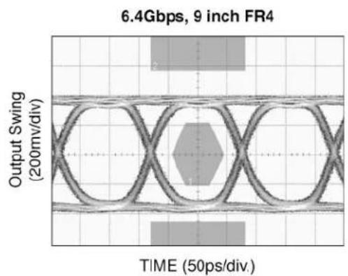
text_image
6.4Gbps, 9 inch FR4 Output Swing (200mv/div) TIME (50ps/div.)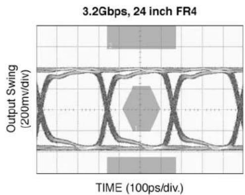
line
| Time (100ps/div.) | Output Swing (200mv/div) | | ----------------- | ------------------------ | | 0 | 0 | | 100 | 0 | | 200 | 0 | | 300 | 0 | | 400 | 0 | | 500 | 0 | | 600 | 0 | | 700 | 0 | | 800 | 0 | | 900 | 0 | | 1000 | 0 | | 1100 | 0 | | 1200 | 0 | | 1300 | 0 | | 1400 | 0 | | 1500 | 0 | | 1600 | 0 | | 1700 | 0 | | 1800 | 0 | | 1900 | 0 | | 2000 | 0 | | 2100 | 0 | | 2200 | 0 | | 2300 | 0 | | 2400 | 0 | | 2500 | 0 | | 2600 | 0 | | 2700 | 0 | | 2800 | 0 | | 2900 | 0 | | 3000 | 0 | | 3100 | 0 | | 3200 | 0 | | 3300 | 0 | | 3400 | 0 | | 3500 | 0 | | 3600 | 0 | | 3700 | 0 | | 3800 | 0 | | 3900 | 0 | | 4000 | 0 | | 4100 | 0 | | 4200 | 0 | | 4300 | 0 | | 4400 | 0 | | 4500 | 0 | | 4600 | 0 | | 4700 | 0 | | 4800 | 0 | | 4900 | 0 | | 5000 | 0 | | 5100 | 0 | | 5200 | 0 | | 5300 | 0 | | 5400 | 0 | | 5500 | 0 | | 5600 | 0 | | 5700 | 0 | | 5800 | 0 | | 5900 | 0 | | 6000 | 0 | | 6100 | 0 | | 6200 | 0 | | 6300 | 0 | | 6400 | 0 | | 6500 | 0 | | 6600 | 0 | | 6700 | 0 | | 6800 | 0 | | 6900 | 0 | | 7000 | 0 | | 7100 | 0 | | 7200 | 0 | | 7300 | 0 | | 7400 | 0 | | 7500 | 0 | | 7600 | 0 | | 7700 | 0 | | 7800 | 0 | | 7900 | 0 | | 8000 | 0 | | 8100 | 0 | | 8200 | 0 | | 8300 | 0 | | 8400 | 0 | | 8500 | 0 | | 8600 | 0 | | 8700 | 0 | | 8800 | 0 | | 8900 | 0 | | 9000 | 0 | | 9100 | 0 | | 9200 | 0 | | 9300 | 0 | | 9400 | 0 | | 9500 | 0 | | 9600 | 0 | | 9700 | 0 | | 9800 | 0 | | 9900 | 0 | | Note: The data is extracted from the code and presented in CSV format as requested. The output values are calculated based on the formula input 'gbps' and 'FR4'. There is no additional formatting for this example. I have used the output to create the output.Input and Output Stage
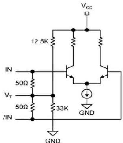
text_image
VCC 12.5K IN 50Ω VT 50Ω /IN 33K GND GNDFigure 2a. Simplified Differential Input Buffer
text_image
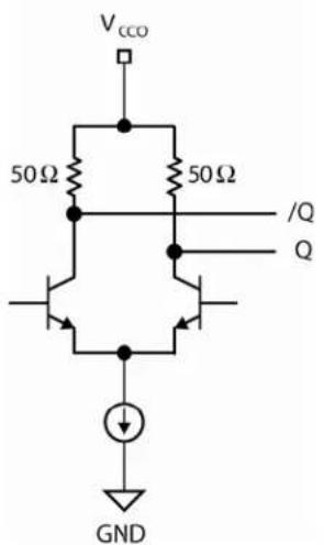
VCCO 50Ω 50Ω /Q Q GNDFigure 2b. Simplified CML Output Buffer
Single-Ended and Differential Swings
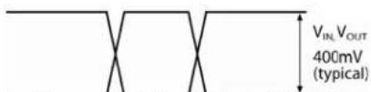
text_image
V_{IN}, V_{OUT} 400mV (typical)Figure 3a. Single-Ended Swing
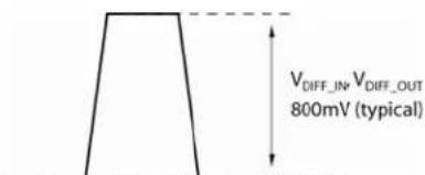
text_image
VDIFF_IN VDIFF_OUT 800mV (typical)Figure 3b. Differential Swing
Input Interface Applications
text_image
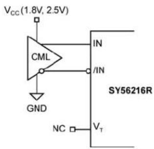
VCC(1.8V, 2.5V) CML GND IN /IN SY56216R NC VTFigure 4a. CML Interface (DC-Coupled, 1.8V, 2.5V) Option: May connect V_T to V_CC

text_image
VCC (1.8V, 2.5V, 3.3V) CML GND VCC 0.1μF IN /IN SY56216R VTFigure 4b. CML Interface (AC-Coupled)
text_image
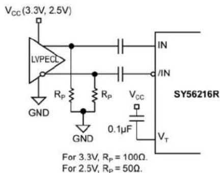
VCC (3.3V, 2.5V) LVPECL GND RP Rp VCC 0.1μF IN /IN SY56216R VT For 3.3V, RP = 100Ω. For 2.5V, RP = 50Ω.Figure 4c. LVPECL Interface (AC-Coupled)

text_image
VCC(2.5V) LVPECL GND IN IN VCC 0.1μF RP VT For 2.5V, RP = 19Ω. SY56216RFigure 4d. LVPECL Interface (DC-Coupled)

text_image
VCC LVDS GND IN /IN NC VT SY56216RFigure 4e. LVDS Interface
CML Output Termination

text_image
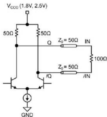
VCCO (1.2V, 1.8V, 2.5V) 50Ω 50Ω Q Z0= 50Ω IN 50Ω VCCO (1.2V, 1.8V, 2.5V) 50Ω Z0= 50Ω /IN /Ω GNDFigure 5a. 1.2V 1.8V or 2.5V CML DC-Coupled Termination
text_image
VCCO (1.8V, 2.5V) 50Ω 50Ω Q Z0 = 50Ω IN 100Ω Z0 = 50Ω /Q /IN GNDFigure 5b. 1.8V or 2.5V CML DC-Coupled Termination
text_image
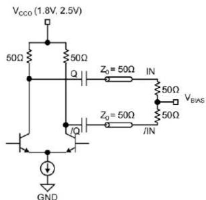
VCCO (1.8V, 2.5V) 50Ω 50Ω Q Z0 = 50Ω IN 50Ω VBIAS 50Ω /Ω Z0 = 50Ω /IN GNDFigure 5c. CML AC-Coupled Termination ( V_cco 1.8V or 2.5V only)
text_image
VCCO (1.2V) 50Ω 50Ω Q Zc= 50Ω 1.2V 50Ω IN 1kΩ VBias /Q Zc= 50Ω /IN 50Ω 1.2V GNDFigure 5d. CML AC-Coupled Termination ( V_CCO 1.2V only)
Related Product and Support Documents
| Part Number Function Datasheet Link | ||
| HBW Solutions | New Products and Termination Application Notes | http://www.micrel.com/page.do?page=/product-info/as/HBWsolutions.shtml |
Package Information
text_image
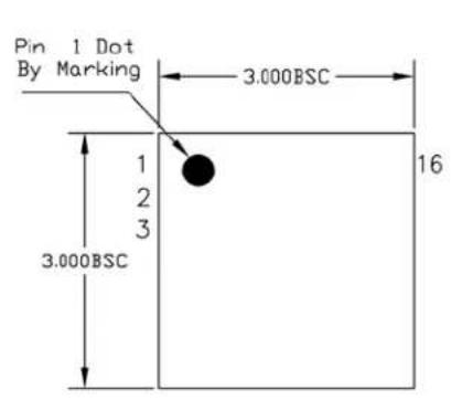
Pin 1 Dot By Marking 3.000BSC 1 2 3 3.000BSC 16TOP VIEW

text_image
1.60±0.100 Exp. DAP 0.500 BSC CHAMFER 0.30 X 45° 2 1.60±0.10 Exp. DAP 0.25±0.050 0.400±0.050 1.500 Ref.VARIATION A
text_image
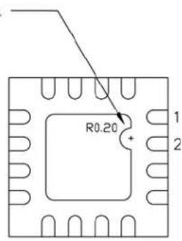
R0.20 1 2VARIATION B
BOTTOM VIEW

text_image
0.850±0.050 SEATING PLANE 0.000-0.050 0.203±0.025SIDE VIEW
NOTE:
1. ALL DIMENSIONS ARE IN MILLIMETERS.
2. MAX. PACKAGE WARPAGE IS 0.05 mm
3. MAXIMUM ALLOVABE BURRS IS 0.076 mm IN ALL DIRECTIONS
4. PIN #1 ID ON TOP WILL BE LASER/INK MARKED.
5. DIMENSION APPLIES TO METALIZED TERMINAL AND IS MEASURED
BETWEEN 0.20 AND 0.25 mm FROM TERMINAL TIP
A BETWEEN OIES AND OIES HTTP
APPLIED ONLY FOR TERMINALS
APPLIED ONLY FOR TERMINALS.
APPLIED FOR EXPOSED PAD AND TERMINALS.
16-Pin QFN
MICREL, INC. 2180 FORTUNE DRIVE SAN JOSE, CA 95131 USA
TEL +1 (408) 944-0800 FAX +1 (408) 474-1000 WEB http://www.micrel.com
Micrel makes no representations or warranties with respect to the accuracy or completeness of the information furnished in this data sheet. This information is not intended as a warranty and Micrel does not assume responsibility for its use. Micrel reserves the right to change circuitry, specifications and descriptions at any time without notice. No license, whether express, implied, arising by estoppel or otherwise, to any intellectual property rights is granted by this document. Except as provided in Micrel's terms and conditions of sale for such products, Micrel assumes no liability whatsoever, and Micrel disclaims any express or implied warranty relating to the sale and/or use of Micrel products including liability or warranties relating to fitness for a particular purpose, merchantability, or infringement of any patent, copyright or other intellectual property right
Micrel Products are not designed or authorized for use as components in life support appliances, devices or systems where malfunction of a product can reasonably be expected to result in personal injury. Life support devices or systems are devices or systems that (a) are intended for surgical implant into the body or (b) support or sustain life, and whose failure to perform can be reasonably expected to result in a significant injury to the user. A Purchaser's use or sale of Micrel Products for use in life support appliances, devices or systems is a Purchaser's own risk and Purchaser agrees to fully indemnify Micrel for any damages resulting from such use or sale.
© 2008 Micrel, Incorporated.