MCP6XXX - Carte d'évaluation Microchip - Free user manual and instructions
Find the device manual for free MCP6XXX Microchip in PDF.

User questions about MCP6XXX Microchip
0 question about this device. Answer the ones you know or ask your own.
Ask a new question about this device
Download the instructions for your Carte d'évaluation in PDF format for free! Find your manual MCP6XXX - Microchip and take your electronic device back in hand. On this page are published all the documents necessary for the use of your device. MCP6XXX by Microchip.
USER MANUAL MCP6XXX Microchip
Note the following details of the code protection feature on Microchip devices:
• Microchip products meet the specification contained in their particular Microchip Data Sheet.
- Microchip believes that its family of products is one of the most secure families of its kind on the market today, when used in the intended manner and under normal conditions.
- There are dishonest and possibly illegal methods used to breach the code protection feature. All of these methods, to our knowledge, require using the Microchip products in a manner outside the operating specifications contained in Microchip's Data Sheets. Most likely, the person doing so is engaged in theft of intellectual property.
• Microchip is willing to work with the customer who is concerned about the integrity of their code.
- Neither Microchip nor any other semiconductor manufacturer can guarantee the security of their code. Code protection does not mean that we are guaranteeing the product as “unbreakable.”
Code protection is constantly evolving. We at Microchip are committed to continuously improving the code protection features of our products. Attempts to break Microchip's code protection feature may be a violation of the Digital Millennium Copyright Act. If such acts allow unauthorized access to your software or other copyrighted work, you may have a right to sue for relief under that Act.
Information contained in this publication regarding device applications and the like is provided only for your convenience and may be superseded by updates. It is your responsibility to ensure that your application meets with your specifications. MICROCHIP MAKES NO REPRESENTATIONS OR WARRANTIES OF ANY KIND WHETHER EXPRESS OR IMPLIED, WRITTEN OR ORAL, STATUTORY OR OTHERWISE, RELATED TO THE INFORMATION, INCLUDING BUT NOT LIMITED TO ITS CONDITION, QUALITY, PERFORMANCE, MERCHANTABILITY OR FITNESS FOR PURPOSE. Microchip disclaims all liability arising from this information and its use. Use of Microchip devices in life support and/or safety applications is entirely at the buyer's risk, and the buyer agrees to defend, indemnify and hold harmless Microchip from any and all damages, claims, suits, or expenses resulting from such use. No licenses are conveyed, implicitly or otherwise, under any Microchip intellectual property rights.
QUALITY MANAGEMENT SYSTEM CERTIFIED BY DNV
=ISO/TS 16949:2002=
Trademarks
The Microchip name and logo, the Microchip logo, Accuron, dsPIC, KEELOQ, KEELOQ logo, microID, MPLAB, PIC, PICmicro, PICSTART, PRO MATE, rfPIC and SmartShunt are registered trademarks of Microchip Technology Incorporated in the U.S.A. and other countries.
AmpLab, FilterLab, Linear Active Thermistor, Migratable Memory, MXDEV, MXLAB, SEEVAL, SmartSensor and The Embedded Control Solutions Company are registered trademarks of Microchip Technology Incorporated in the U.S.A.
Analog-for-the-Digital Age, Application Maestro, CodeGuard, dsPICDEM, dsPICDEM.net, dsPICworks, ECAN, ECONOMONITOR, FanSense, FlexROM, fuzzyLAB, In-Circuit Serial Programming, ICSP, ICEPIC, Mindi, MiWi, MPASM, MPLAB Certified logo, MPLIB, MPLINK, PICkit, PICDEM, PICDEM.net, PICLAB, PICtail, PowerCal, PowerInfo, PowerMate, PowerTool, REAL ICE, rfLAB, Select Mode, Smart Serial, SmartTel, Total Endurance, UNI/O, WiperLock and ZENA are trademarks of Microchip Technology Incorporated in the U.S.A. and other countries.
SQTP is a service mark of Microchip Technology Incorporated in the U.S.A.
All other trademarks mentioned herein are property of their respective companies.
© 2007, Microchip Technology Incorporated, Printed in the U.S.A., All Rights Reserved.
Printed on recycled paper.
Microchip received ISO/TS-16949:2002 certification for its worldwide headquarters, design and wafer fabrication facilities in Chandler and Tempe, Arizona; Gresham, Oregon and design centers in California and India. The Company's quality system processes and procedures are for its PIC® MCUs and dsPIC® DSCs, KEELOQ® code hopping devices, Serial EEPROMs, microperipherals, nonvolatile memory and analog products. In addition, Microchip's quality system for the design and manufacture of development systems is ISO 9001:2000 certified.
Table of Contents
Preface 1
Introduction....1
Document Layout .... 1
Conventions Used in this Guide.... 2
Recommended Reading.... 3
The Microchip Web Site 3
Customer Support 3
Document Revision History.... 3
Chapter 1. Product Overview ...... 5
1.1 Introduction 5
1.2 MCP6XXX Amplifier Evaluation Board 1 Kit Contents .... 5
1.3 Microchip's Web-Based Mindi™ Analog Simulator 6
1.4 MCP6XXX Amplifier Evaluation Board 1 Description ...... 6
Chapter 2. Installation and Operation ....7
2.1 Introduction 7
2.2 Required Tools 7
2.3 MCP6XXX Amplifier Evaluation Board 1 Set-up ....7
2.4 MCP6XXX Amplifier Evaluation Board 1 Operation .... 18
Appendix A. Schematic and Layouts 29
A.1 Introduction 29
A.2 Board - Schematic 30
A.3 Board - Top Silk Layer 31
A.4 Board - Top Metal Layer 32
A.5 Board - Bottom Metal Layer 33
Appendix B. Bill Of Materials (BOM) 35
B.1 MCP6XXX Amplifier Evaluation Board 1 BOM 35
Worldwide Sales and Service 38
MCP6XXX Amplifier Evaluation Board 1 User's Guide
NOTES:
Preface
NOTICE TO CUSTOMERS
All documentation becomes dated, and this manual is no exception. Microchip tools and documentation are constantly evolving to meet customer needs, so some actual dialogs and/or tool descriptions may differ from those in this document. Please refer to our web site (www.microchip.com) to obtain the latest documentation available.
Documents are identified with a "DS" number. This number is located on the bottom of each page, in front of the page number. The numbering convention for the DS number is "DSXXXXXA", where "XXXXX" is the document number and "A" is the revision level of the document.
For the most up-to-date information on development tools, see the MPLAB ^® IDE on-line help. Select the Help menu, and then Topics to open a list of available on-line help files.
INTRODUCTION
This chapter contains general information that will be useful to know before using the MCP6XXX Amplifier Evaluation Board 1. Items discussed in this chapter include:
- Document Layout
- Conventions Used in this Guide
• Recommended Reading
• The Microchip Web Site - Customer Support
- Document Revision History
DOCUMENT LAYOUT
This document describes how to use the MCP6XXX Amplifier Evaluation Board 1. The manual layout is as follows:
- Chapter 1. "Product Overview" - Provides all important information about the MCP6XXX Amplifier Evaluation Board 1.
- Chapter 2. “Installation and Operation” – Covers the installation and operation of the MCP6XXX Amplifier Evaluation Board 1. It lists the required tools, shows how to set up the board, and demonstrates how to verify the operation.
- Appendix A. “Schematic and Layouts” – Shows the schematic and board layouts for the MCP6XXX Amplifier Evaluation Board 1.
- Appendix B. “Bill Of Materials (BOM)” – Lists the parts used to build the MCP6XXX Amplifier Evaluation Board 1.
CONVENTIONS USED IN THIS GUIDE
This manual uses the following documentation conventions:
DOCUMENTATION CONVENTIONS
| Description Represents Examples | ||
| Arial font: | ||
| Italic characters Referenced books | MPLAB | ^ IDE User's Guide |
| Emphasized text ...is the only compiler... | ||
| Initial caps A window the Output | t window | |
| A dialog the Settings dialog | ||
| A menu selection select Enable | Programmer | |
| Quotes A field name in a window | w ordialog | "Save project before build" |
| Underlined, italic text with right angle bracket | A menu path File>Save | —— |
| Bold characters A dialog button | Click OK | |
| A tab | Click the Power tab | |
| N'Rnnnn | A number in verilog format, where N is the total number of digits, R is the radix and n is a digit. | 4'b0010, 2'hF1 |
| Text in angle brackets <> | A key on the keyboard | Press,, |
| Courier New font: | ||
| Plain Courier New | Sample source code | #define START |
| Filenames | autoexec.bat | |
| File paths | c:\mccl8\h | |
| Keywords | _asm, _endasm, static | |
| Command-line options | -Opa+, -Opa- | |
| Bit values | 0, 1 | |
| Constants | 0xFF, 'A' | |
| Italic Courier New | A variable argument | file.o, where file can be any valid filename |
| Square brackets [] | Optional arguments | mccl8 [options] file [options] |
| Curly brackets and pipe character: { | } | Choice of mutually exclusive arguments; an OR selection | errorlevel {0|1} |
| Ellipses... Replaces repeated text | var_name [, | var_name...] |
| Represents code supplied by user | void main (void){ ...} | |
RECOMMENDED READING
This user's guide describes how to use MCP6XXX Amplifier Evaluation Board 1. Other useful documents are listed below. The following Microchip documents are available and recommended as supplemental reference resources.
MCP6021 Data Sheet "Rail-to-Rail Input/Output, 10 MHz Op Amps" (DS21685)
This data sheet provides detailed information regarding the MCP6021 product family.
Microchip provides online support via our web site at www.microchip.com. This web site is used as a means to make files and information easily available to customers. Accessible by using your favorite Internet browser, the web site contains the following information:
- Product Support – Data sheets and errata, application notes and sample programs, design resources, user's guides and hardware support documents, latest software releases and archived software
- General Technical Support – Frequently Asked Questions (FAQs), technical support requests, online discussion groups, Microchip consultant program member listing
- Business of Microchip – Product selector and ordering guides, latest Microchip press releases, listing of seminars and events, listings of Microchip sales offices, distributors and factory representatives
CUSTOMER SUPPORT
Users of Microchip products can receive assistance through several channels:
• Distributor or Representative
- Local Sales Office
• Field Application Engineer (FAE)
- Technical Support
• Development Systems Information Line
Customers should contact their distributor, representative or field application engineer for support. Local sales offices are also available to help customers. A listing of sales offices and locations is included in the back of this document.
Technical support is available through the web site at: http://support.microchip.com.
DOCUMENT REVISION HISTORY
Revision A (July 2007)
- Initial Release of this Document.
NOTES:
Chapter 1. Product Overview
1.1 INTRODUCTION
The MCP6XXX Amplifier Evaluation Board 1 is described by the following:
- Assembly #: 114-00147
- Order #: MCP6XXXEV-AMP1
• Name: MCP6XXX Amplifier Evaluation Board 1
Items discussed in this chapter include:
• Section 1.2 "MCP6XXX Amplifier Evaluation Board 1 Kit Contents"
- Section 1.3 "Microchip's Web-Based Mindi™ Analog Simulator"
• Section 1.4 "MCP6XXX Amplifier Evaluation Board 1 Description"
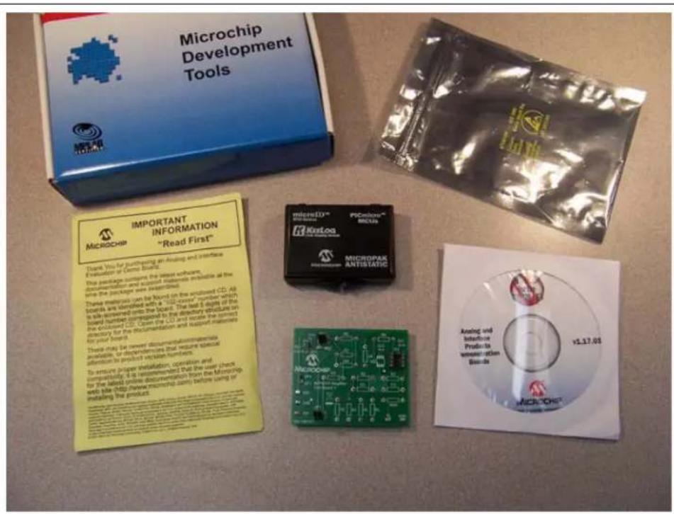
1.2 MCP6XXX AMPLIFIER EVALUATION BOARD 1 KIT CONTENTS
- MCP6XXX Amplifier Evaluation Board 1 - One partially assembled board
- Important Information "Read First"
- Accessory Bag - Contains loose parts for populating sockets on board
- Analog and Interface Products Demonstration Boards CD-ROM (DS21912) - MCP6XXX Amplifier Evaluation Board 1 User's Guide (DS51667)
text_image
Microchip Development Tools MICROCHIP IMPORTANT INFORMATION "Read First" Thank You for purchasing an Amazing and Interface Evaluation of Cramo Studio. This package contains the latest software documentation and supported materials available at the time the package was requested. These materials can be found on the enclosed CD. All buttons are identified with a "102-core" number which is set up to the next numbered button in the directory structure on the CD. Open the CD and includes the optimal directory for the documentation and support modules. These tools are current document/data/materials available or dependent on that require special attention to product version numbers. To ensure proper installation, operation and compatibility, it is recommended that the user check for the latest online documentation from the Microchip installing this product. Microchip MICROCHIP PVCellors™ MCCUs MICROPAX ANTISTATIC Analog and Interface Products: Amemation Bands V$1.17.01 MICROCHIPFIGURE 1-1: MCP6XXX Amplifier Evaluation Board 1 Kit.
1.3 MICROCHIP'S WEB-BASED MINDI™ ANALOG SIMULATOR
The Mindi™ Analog Simulator tool is an innovative software tool that simplifies analog circuit design. The Mindi™ Analog Simulator tool supports the following application circuits: 1) Active Filters, 2) Amplifiers, 3) Battery Chargers, and 4) DC-to-DC Converters. The Mindi™ Amplifier Designer provides full schematic diagrams of the amplifier application circuit with recommended component values and displays the responses in frequency and time domains.
The Mindi™ Analog Simulator tool is a free web-based design tool available on the Microchip web site at http://www.microchip.com under “Online Simulation Tools” or by going directly to the Mindi™ web site at http://www.microchip.com/mindi.
The circuit simulator within the Mindi™ Analog Simulator tool can be downloaded and installed on a personal computer (PC) for more convenient simulations. Modified circuit files can also be downloaded to the PC.
1.4 MCP6XXX AMPLIFIER EVALUATION BOARD 1 DESCRIPTION
The MCP6XXX Amplifier Evaluation Board 1 is designed to support inverting/non-inverting amplifiers, voltage follower, inverting/non-inverting comparators, inverting/non-inverting differentiators.
However, at this time, the Mindi™ Amplifier Designer does not support the non-inverting comparator or the non-inverting differentiator.
MCP6XXX Amplifier Evaluation Board 1 has the following features:
- All amplifier resistors and capacitors are socketed
-
All of the component labels on board keep consistent with those on schematic generated in the Mindi™ Amplifier Designer
• Supports all Microchip single op amps -
PDIP-8 package (e.g., MCP6021) are socketed
- SOIC-8 package can be accommodated; see Section 2.4.3 "Amplifier Modification: Using 8-Pin SOIC Op Amps"
• Test points for connecting lab equipment
- Single supply configuration
Figure 1-2 shows the block diagram of the MCP6XXX Amplifier Evaluation Board 1. Lab equipment can be attached (via test points) to measure the amplifier response.

flowchart
graph TD
    A["Mid-Supply Ref and Test Point"] --> C["Amplifier Resistor and Capacitor Sockets"]
    B["Power Supply and Test Point"] --> C
    D["Signal Input and Test Point"] --> C
    E["Signal Output and Test Point"] --> C
FIGURE 1-2: MCP6XXX Amplifier Evaluation Board 1 Block Diagram.
Chapter 2. Installation and Operation
2.1 INTRODUCTION
This chapter shows how to set up the MCP6XXX Amplifier Evaluation Board 1 and verify its operation. This chapter includes the following topics:
- Required Tools
• MCP6XXX Amplifier Evaluation Board 1 Set-Up - MCP6XXX Amplifier Evaluation Board 1 Operation
2.2 REQUIRED TOOLS
- Lab power supply
- Lab signal source (e.g., function generator)
- Lab measurement equipment (e.g., oscilloscope)
2.3 MCP6XXX AMPLIFIER EVALUATION BOARD 1 SET-UP
The MCP6XXX Amplifier Evaluation Board 1 is designed to support inverting/non-inverting amplifiers, voltage follower, inverting/non-inverting comparators, inverting/non-inverting differentiators
At this time, the Mindi™ Amplifier Designer does not support the non-inverting comparator or the non-inverting differentiator.
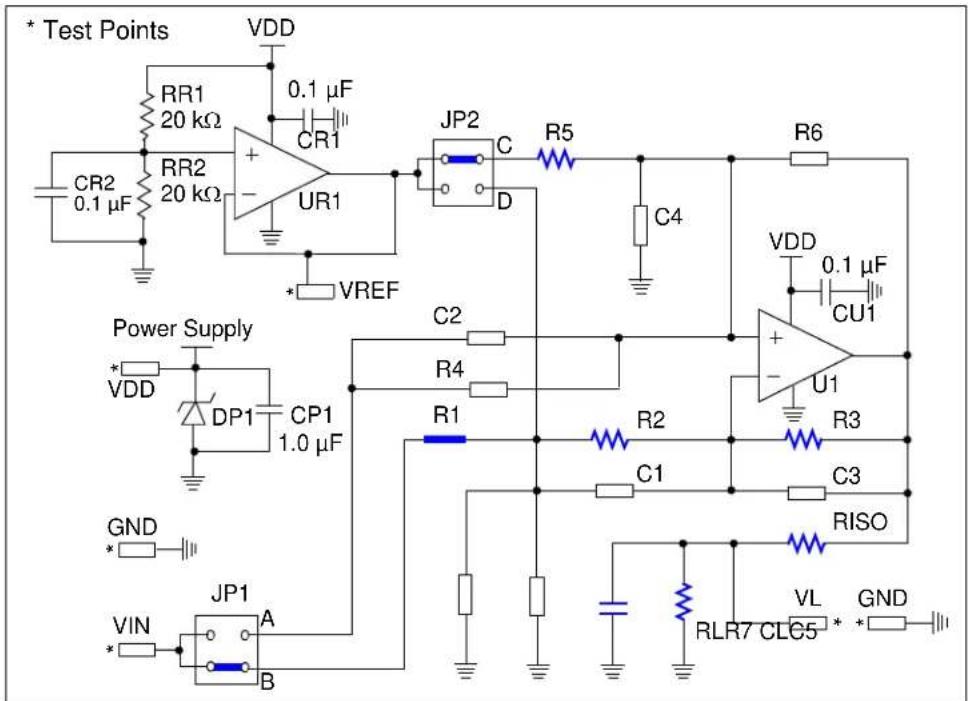
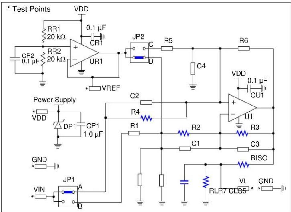
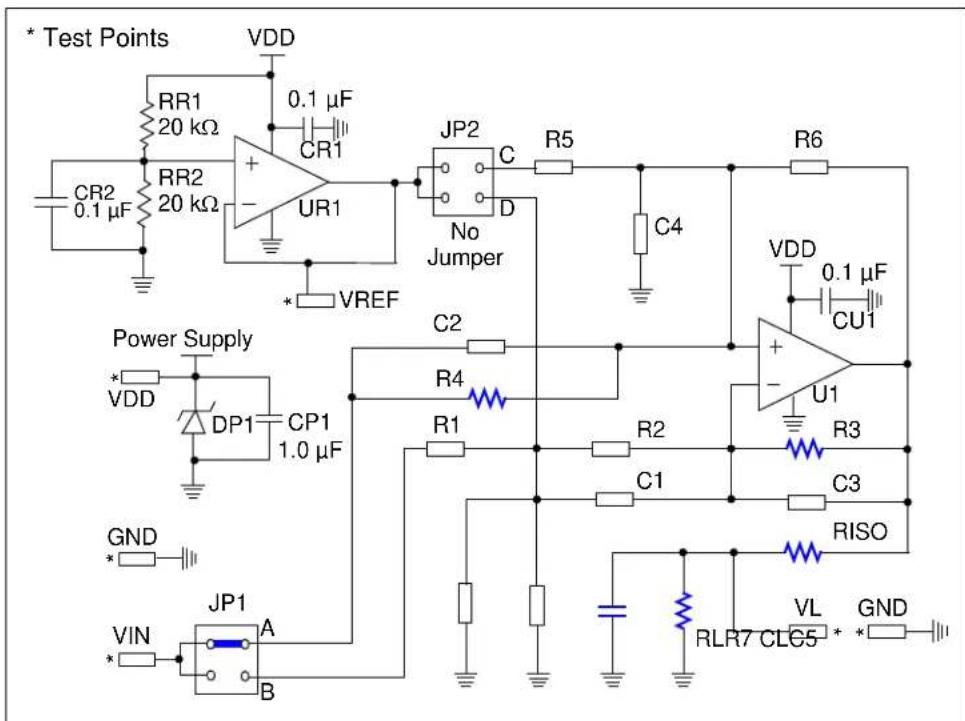
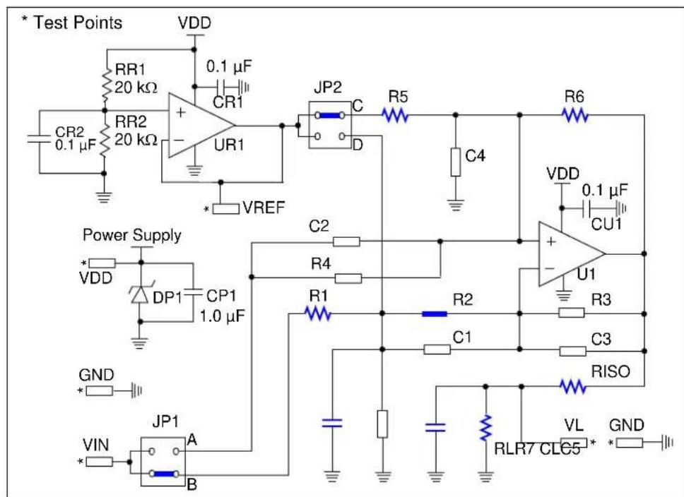
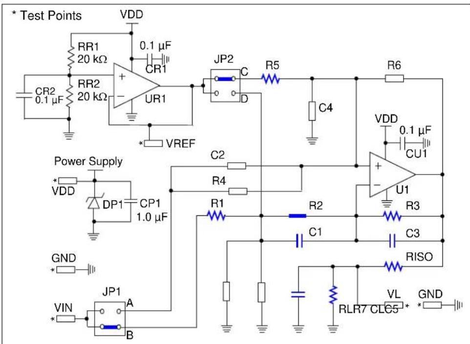
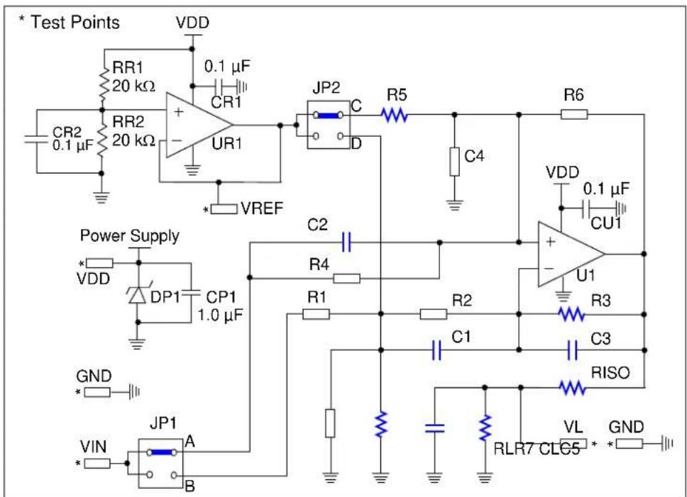
This section details the conversion of these topologies to the MCP6XXX Amplifier Evaluation Board 1. Figure 2-1 shows the circuit diagram for the board.

text_image
* Test Points VDD RR1 20 kΩ 0.1 μF CR1 CR2 0.1 μF RR2 20 kΩ + - UR1 JP2 C R5 D C4 R6 VDD 0.1 μF CU1 Power Supply * VDD DP1 CP1 1.0 μF GND * VIN JP1 A B C2 R4 R1 R2 C1 C3 RISO VL RLR7 CLE5* * GNDFIGURE 2-1: MCP6XXX Amplifier Evaluation Board 1 Circuit Diagram.
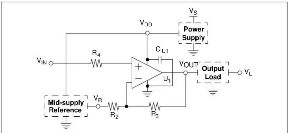
The power supply voltage should be in the allowed range for the installed op amps. Any of Microchip's op amps that operate below 5.5V can be used. Moreover, power supply is protected by a zener diode with nominal voltage 6.2V and bypassed by a 1.0 F capacitor. (See Figure 2-3: "Power Supply Block.")
The mid-supply reference consists of a voltage divider and a buffer amplifier. (See Figure 2-4: "Mid-Supply Reference Block.")
The resistors and capacitors that are part of an amplifier are placed in pin sockets which are labeled. All of the component labels on board keep consistent with those on schematic generated in the Mindi™ Amplifier Designer. The op amps are bypassed by 0.1 μF capacitors and the single op amp U1 can have either a PDIP-8 or SOIC-8 package.
- PDIP-8 packages are inserted into the DIP-8 socket to the right of the U1 label
- SOIC-8 packages can be accommodated; see Section 2.4.3 "Amplifier Modification: Using 8-Pin SOIC Op Amps"
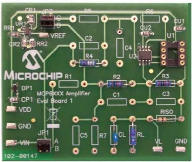
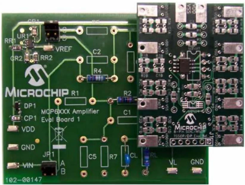
The (surface mount) test points for power supply, ground, input signal and output signal allow lab equipment to be connected to the board. The MCP6XXX Amplifier Evaluation Board 1 top view is shown in Figure 2-2.
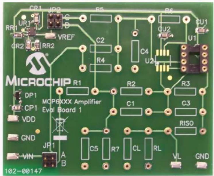
text_image
CR1 JP2 R5 R6 UR1 C D RR1 VREF C2 CU1 GR2 RR2 R4 U2 U1 MICROCHIP R1 R2 R3 DP1 MCP6XXX Amplifier CP1 Eval Board 1 C1 C3 VDD RISO GND JP1 RL VIN A C5 R7 CL RL VL GND 102-00147FIGURE 2-2: MCP6XXX Amplifier Evaluation Board 1 Top View.
2.3.1 Top Level Amplifier Circuit Diagrams
2.3.1.1 POWER SUPPLY BLOCK
The power supply is protected by a zener diode and bypassed by a capacitor. Figure 2-3 shows the circuit diagram for the power supply. C_P1 = 1.0 F .
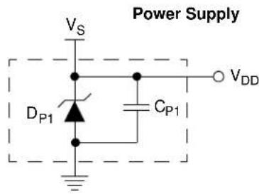
text_image
Power Supply V_S D_{P1} C_{P1} V_{DD}Note: D _P1 is a zener diode with nominal voltage of 6.2V
FIGURE 2-3: Power Supply Block.
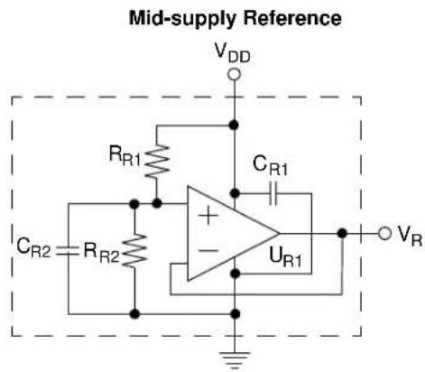
2.3.1.2 MID-SUPPLY REFERENCE BLOCK
The mid-supply reference consists of a voltage divider and a buffer amplifier. Figure 2-4 shows the circuit diagram for the mid-supply reference.
$$ C _ {R 1} = C _ {R 2} = 0. 1 \mu F, R _ {R 1} = R _ {R 2} = 2 0. 0 k \Omega . $$
text_image
Mid-supply Reference VDD RR1 CR1 CR2 RR2 + - UR1 VRFIGURE 2-4: Mid-Supply Reference Block.
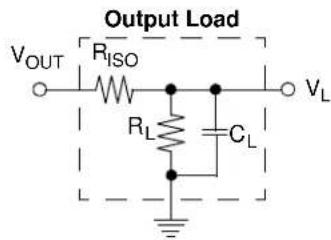
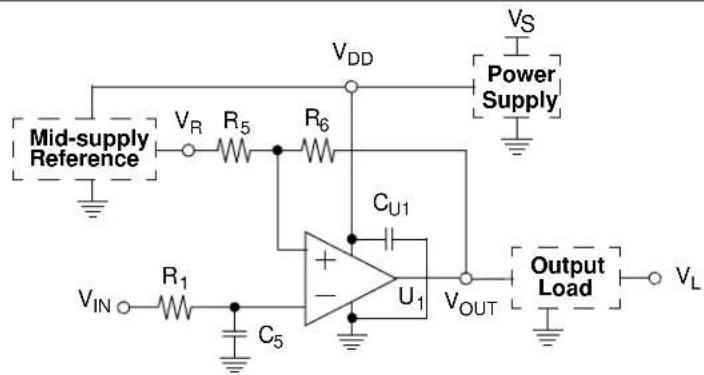
2.3.1.3 OUTPUT LOAD BLOCK
The output load consists of a capacitor and two resistors. Figure 2-5 shows the circuit diagram for the output load. R_ISO is used to stabilize the amplifier when it drives a large capacitive load. R_ISO is a short circuit (0Ω) when C_L is small.
text_image
Output Load VOUT RISO VL RL CLFIGURE 2-5: Output Load Block.
2.3.1.4 INVERTING AMPLIFIER
- Amplifies a voltage with an inverting gain. Input and output voltages are shifted by a reference voltage for single supply.
- The Mindi™ Amplifier Designer gives design recommendations for an inverting amplifier circuit; see the circuit diagram shown in Figure 2-6
- Fill the sockets with the recommended resistors and capacitors
- Set JP1 and JP2 in the correct positions (for the given example, JP1: Position B, JP2: Position C)

text_image
Mid-supply Reference V_R R_5 U_1 V_DD C_{U1} V_S Power Supply Output Load V_L V_IN R_2 R_3FIGURE 2-6: Inverting Amplifier Circuit Diagram.
Figure 2-7 shows an example of the inverting amplifier circuit diagram supported by MCP6XXX Amplifier Evaluation Board 1.
text_image
* Test Points VDD RR1 20 kΩ 0.1 μF CR1 RR2 20 kΩ + - UR1 JP2 C R5 D C4 R6 VDD 0.1 μF CU1 Power Supply VDD DP1 CP1 1.0 μF GND JP1 A B C2 R4 R1 R2 C1 R3 C3 RISO VIN VL CLC5 GNDFIGURE 2-7: Inverting Amplifier Example Supported by the MCP6XXX Amplifier Evaluation Board 1.
2.3.1.5 NON-INVERTING AMPLIFIER
- Amplifies a voltage with a non-inverting gain > + 1 V/V. Input and output voltages are shifted by a reference voltage for single supply
- The Mindi™ Amplifier Designer gives design recommendations for the non-inverting amplifier circuit; see the circuit diagram shown in Figure 2-8
- Fill the sockets with the recommended resistors and capacitors
- Set JP1 and JP2 in the correct positions (for the given example, JP1: Position A, JP2: Position D)
text_image
VDD VS Power Supply CU1 VOUT Output Load VIN R4 U1 VOUT Mid-supply Reference VR R2 R3 VLFIGURE 2-8: Non-Inverting Amplifier Circuit Diagram.
Figure 2-9 shows an example of the inverting amplifier circuit diagram supported by MCP6XXX Amplifier Evaluation Board 1.
text_image
* Test Points VDD RR1 20 kΩ 0.1 μF CR1 RR2 20 kΩ CR2 0.1 μF + UR1 JP2 C R5 C4 R6 VDD 0.1 μF CU1 Power Supply VDD DP1 CP1 1.0 μF GND JP1 A VIN B C2 R4 R1 R2 C1 R3 C3 RISO VL RLR7 CLC5 GNDFIGURE 2-9: Non-Inverting Amplifier Example Supported by the MCP6XXX Amplifier Evaluation Board 1.
- Known as a Unity Gain Buffer and as a Voltage Follower. Amplifies a voltage with a gain of 1 V/V
- The Mindi™ Amplifier Designer gives design recommendations for the voltage follower circuit; see the circuit diagram shown in Figure 2-10
- Fill the sockets with the recommended resistors and capacitors
- Set JP1 and JP2 in the correct positions (for the given example, JP1: Position A, JP2: Position N/A)
text_image
VDD VS Power Supply CU1 VIN + - U1 VOUT Output Load VL R4 R3FIGURE 2-10: Voltage Follower Circuit Diagram.
Figure 2-11 shows an example of the voltage amplifier circuit diagram supported by MCP6XXX Amplifier Evaluation Board 1.
text_image
* Test Points VDD RR1 20 kΩ 0.1 μF CR1 + - UR1 JP2 C R5 No Jumper C4 R6 VDD 0.1 μF CU1 Power Supply * VDD DP1 CP1 1.0 μF GND * VIN JP1 A B C2 R4 R1 R2 C1 U1 R3 C3 RISO VL RLR7 CLC5 * GNDFIGURE 2-11: Voltage Amplifier Example Supported by the MCP6XXX Amplifier Evaluation Board 1.
2.3.1.7 INVERTING COMPARATOR
- Compares the input voltage to another (reference) voltage and forces the output to one of two digital states. Input signal is applied to the inverting input. The comparison includes a user selected amount of hysteresis. Input and output voltages are shifted by a reference for single supply
- The Mindi™ Amplifier Designer gives design recommendations for the inverting comparator circuit; see the circuit diagram shown in Figure 2-12
- Fill the sockets with the recommended resistors and capacitors
- Set JP1 and JP2 in the correct positions (for the given example, JP1: Position B, JP2: Position C)
Note: The MCP6XXX Amplifier Evaluation Board 1 currently only supports the inverting comparator with center trip point = 2.5V.
text_image
Mid-supply Reference V_R R_5 R_6 V_DD V_S Power Supply C_U1 U_1 V_IN R_1 V_OUT Output C_5 V_LFIGURE 2-12: Inverting Comparator Circuit Diagram.
Figure 2-13 shows an example of the inverting comparator circuit diagram supported by MCP6XXX Amplifier Evaluation Board 1.
text_image
* Test Points VDD RR1 20 kΩ 0.1 μF CR1 CR2 0.1 μF RR2 20 kΩ + - UR1 JP2 C R5 C4 R6 VDD 0.1 μF CU1 Power Supply * VDD DP1 CP1 1.0 μF GND * VIN JP1 A B C2 R4 R1 R2 C1 R3 C3 RISO VL RLR7 CLE5* GNDFIGURE 2-13: Inverting Comparator Example Supported by the MCP6XXX Amplifier Evaluation Board 1.
2.3.1.8 NON-INVERTING COMPARATOR (NOT CURRENTLY SUPPORTED)
- Compares the input voltage to another (reference) voltage and forces the output to one of two digital states. Input signal is applied to the non-inverting input. The comparison includes a user selected amount of hysteresis. Input and output voltages are shifted by a reference for single supply
- The Mindi™ Amplifier Designer gives design recommendations for the non-inverting comparator circuit; see the circuit diagram shown in Figure 2-14
- Fill the sockets with the recommended resistors and capacitors
- Set JP1 and JP2 in the correct positions (for the given example, JP1: Position A, JP2: Position D)
Note: The MCP6XXX Amplifier Evaluation Board 1 currently only supports the non-inverting comparator with center trip point = 2.5V.

text_image
VDD VS Power Supply VIN R4 C4 R6 CU1 Mid-supply Reference VR R2 U1 VOUT Output Load VLFIGURE 2-14: Non-Inverting Comparator Circuit Diagram.
Figure 2-15 shows an example of the non-inverting comparator circuit diagram supported by the MCP6XXX Amplifier Evaluation Board 1.

text_image
* Test Points VDD RR1 20 kΩ 0.1 μF CR1 RR2 20 kΩ + - UR1 JP2 C R5 C4 R6 VDD 0.1 μF CR2 0.1 μF * VREF Power Supply * VDD DP1 CP1 1.0 μF GND * VIN JP1 A B C2 R4 R1 R2 C1 U1 R3 C3 RISO VL RLR7 CLE5 * GNDFIGURE 2-15: Non-Inverting Comparator Example Supported by the MCP6XXX Amplifier Evaluation Board 1.
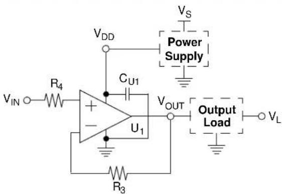
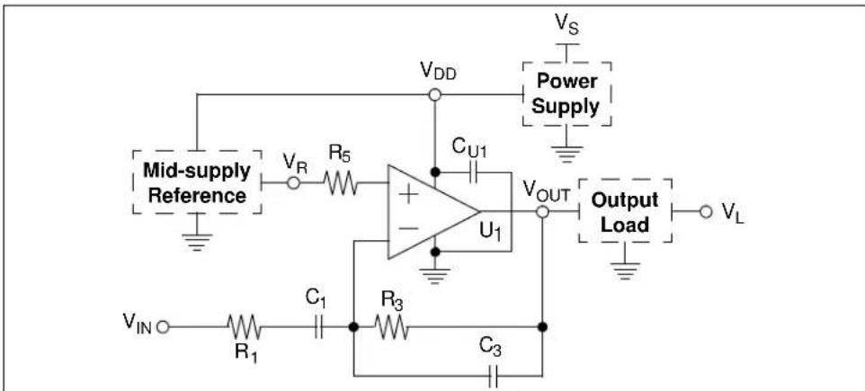
2.3.1.9 INVERTING DIFFERENTIATOR (NOT CURRENTLY SUPPORTED)
- Differentiates and inverts a voltage with a differentiating frequency. Additional components (R_1, C_3) achieve stabilization and noise. Input and output voltages are shifted by a reference for single supply
- The Mindi™ Amplifier Designer gives design recommendations for the inverting differentiator circuit; see the circuit diagram shown in Figure 2-16
- Fill the sockets with the recommended resistors and capacitors
- Set JP1 and JP2 in the correct positions (for the given example, JP1: Position B, JP2: Position C)
text_image
Mid-supply Reference V_R R_5 C_U1 U1 V_DD V_S Power Supply Output Load V_OUT V_L V_IN R_1 C_1 R_3 C_3FIGURE 2-16: Inverting Differentiator Circuit Diagram.
Figure 2-17 shows an example of the inverting differentiator circuit diagram supported by MCP6XXX Amplifier Evaluation Board 1.
text_image
* Test Points VDD RR1 20 kΩ 0.1 μF CR1 CR2 0.1 μF RR2 20 kΩ + - UR1 JP2 C R5 C4 R6 VDD 0.1 μF CU1 Power Supply * VDD DP1 CP1 1.0 μF GND * VIN JP1 A B C2 R4 R1 R2 C1 R3 C3 RISO VL RLR7 CLC5 * GNDFIGURE 2-17: Inverting Differentiator Example Supported by the MCP6XXX Amplifier Evaluation Board 1.
2.3.1.10 NON-INVERTING DIFFERENTIATOR (NOT CURRENTLY SUPPORTED)
- Differentiates and inverts a voltage with a differentiating frequency. Additional components (R_7, C_3) achieve stabilization and noise. Input and output voltages are shifted by a reference for single supply
- The Mindi™ Amplifier Designer gives design recommendations for the non-inverting differentiator circuit; see the circuit diagram shown in Figure 2-18
- Fill the sockets with the recommended resistors and capacitors
- Set JP1 and JP2 in the correct positions (for the given example, JP1: Position A, JP2: Position C)
Note: The MCP6XXX Amplifier Evaluation Board 1 currently only supports the non-inverting differentiator with center trip point = 2.5V.
text_image
VDD VS Power Supply CU1 VIN C2 R5 + - U1 Output Load VL Mid-supply Reference VR R7 C1 R3 C3FIGURE 2-18: Non-Inverting Differentiator Circuit Diagram.
Figure 2-19 shows an example of the non-inverting differentiator circuit diagram supported by MCP6XXX Amplifier Evaluation Board 1.
text_image
* Test Points VDD RR1 20 kΩ 0.1 μF CR1 + - UR1 CR2 0.1 μF RR2 20 kΩ * VREF JP2 C R5 C4 R6 VDD 0.1 μF CU1 Power Supply * VDD DP1 CP1 1.0 μF GND * JP1 A VIN * B C2 R4 R1 R2 C1 C3 RISO VL RLR7 CLG5 * GNDFIGURE 2-19: Non-Inverting Differentiator Example Supported by the MCP6XXX Amplifier Evaluation Board 1.
2.4 MCP6XXX AMPLIFIER EVALUATION BOARD 1 OPERATION
Items discussed in this section include:
• Building the Amplifier
- Testing the Amplifier
- Amplifier Modification: Using 8-Pin SOIC Op Amps
2.4.1 Building the Amplifier
The accessory bag that comes with this kit makes it quick and easy to evaluate the amplifier described below; it was designed in Mindi™ Amplifier Designer.
This amplifier is described as follows:
• Non-Inverting Amplifier (Single Supply Configuration)
• Power Supply Voltage is 5.0V
• Desired Closed Loop Gain is 2 V/V
- Load Capacitance is 56 pF
text_image
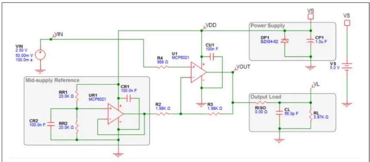
VIN 2.50 V 50.00m V 100.0m s VIN VDD U1 MCP6021 CU1 100n F R4 968 Ω VOUT Power Supply DP1 BZX84-82 CP1 1.0u F VS 5.0 V VS Mid-supply Reference RR1 20.0K Ω UR1 MCP6021 CR1 100.0n F CR2 100.0n F RR2 20.0K Ω R2 1.98K Ω R3 1.98K Ω Output Load VL RI SO 0.00 Ω CL 56.0p F RL 3.97K ΩFIGURE 2-20: Non-Inverting Amplifier Designed In Mindi™ Amplifier Designer.
Figure 2-21 shows the same circuit redrawn to emphasize the non-inverting amplifier.

text_image
VDD VS Power Supply CU1 VOUT Output Load VIN R4 U1 VOUT Mid-supply Reference VR R2 R3 VLFIGURE 2-21: Non-Inverting Amplifier Circuit Diagram Supported by the MCP6XXX Amplifier Evaluation Board 1 Kit.
Each of the components in Figure 2-21 that needs to be inserted in a socket on the MCP6XXX Amplifier Evaluation Board 1 is listed in Table 2-1 and Table 2-2.
TABLE 2-1: AMPLIFIER COMPONENTS LIST
| PCB Labels Component Values | |
| R2 1.98 kΩ | |
| R3 1.98 kΩ | |
| R4 988Ω | |
| RISO 0Ω | |
| RL 3.97 kΩ | |
| CL 56 pF | |
| U1 MCP6021, PDIP-8, 10 MHz | |
TABLE 2-2: JUMPER POSITIONS
| Jumper Position | |
| JP1 A | |
| JP2 D |
Figure 2-22 shows the fully assembled MCP6XXX Amplifier Evaluation Board 1 for the non-inverting amplifier.

text_image
* Test Points VDD RR1 20 kΩ 0.1 μF CR1 + - CR2 0.1 μF RR2 20 kΩ UR1 JP2 C R5 C4 R6 VDD 0.1 μF CU1 Power Supply VDD DP1 CP1 1.0 μF C2 R4 R1 R2 C1 U1 R3 GND JP1 VIN A B C5 R7 CL RL RISO VL GND *FIGURE 2-22: Fully Assembled Non-Inverting Amplifier Supported by the MCP6XXX Amplifier Evaluation Board 1.
The fully assembled MCP6XXX Amplifier Evaluation Board 1 top view is shown in Figure 2-23.
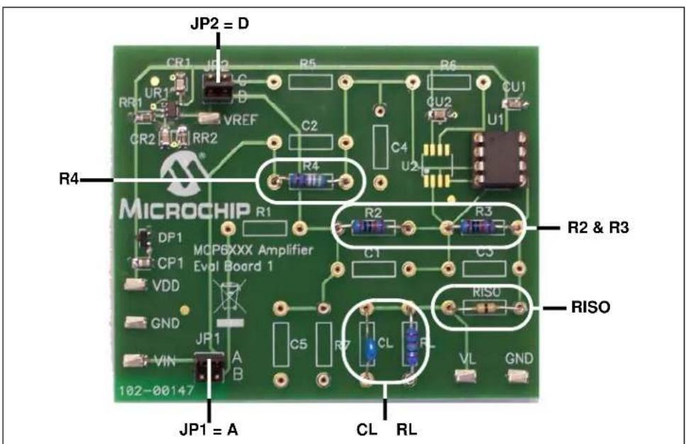
text_image
JP2 = D CR1 JP2 R5 R6 CU1 UR1 C D VREF C2 C4 U1 CR2 RR2 R4 MICROCHIP MCP6XXX Amplifier Eval Board 1 DP1 R1 R2 R3 R2 & R3 CP1 C1 C5 VDD GND JP1 A CL RL VIN A B VL GND 102-00147 JP1 = A CL RLFIGURE 2-23: Picture of the Non-Inverting Amplifier Supported by the MCP6XXX Amplifier Evaluation Board 1.
2.4.2 Testing the Amplifier
2.4.2.1 CHECKING THE TEST POINTS
The (surface mount) test points for power supply, ground, input signal and output signal allow lab equipment to be connected to the board. Figure 2-24 shows the test points to check.
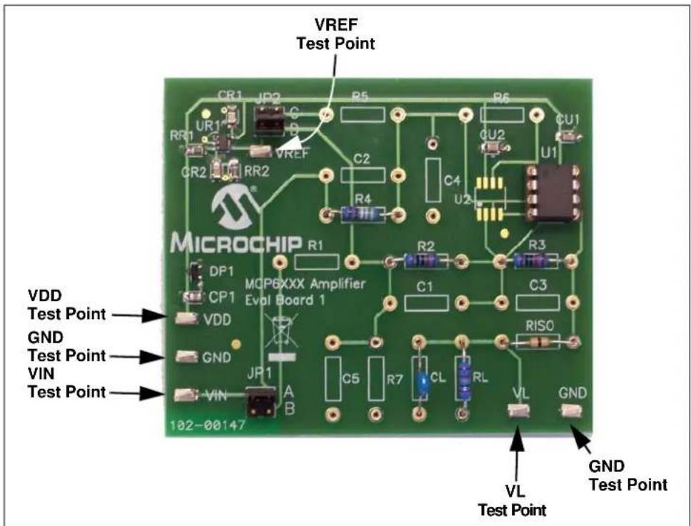
text_image
VREF Test Point CR1 JP2 R5 R6 CU1 RR1 UR1 C D VREF CR2 RR2 C2 U2 U1 R4 R3 MICROCHIP R1 MCP6XXX Amplifier Evol Board 1 DP1 C1 C3 CP1 VDD RISO GND Test Point GND Test Point VIN Test Point JP1 A B VL GND 102-00147 VL Test Point GND Test PointFIGURE 2-24: Checking the Test Points.
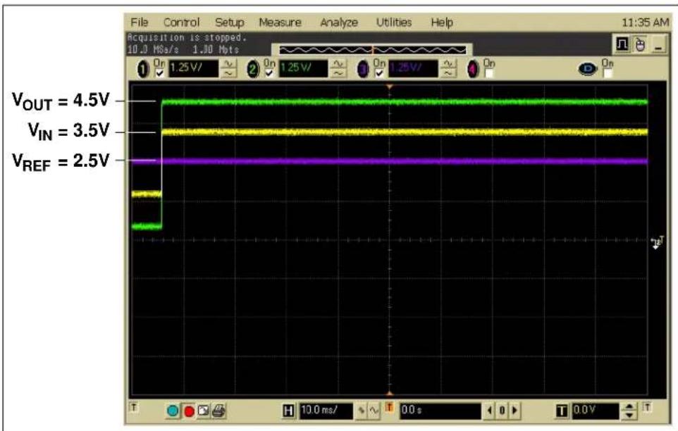
2.4.2.2 TRANSIENT RESPONSES
This non-inverting amplifier was built, and its responses were measured. A MCP6021 op amp, 1% resistors, and 5% capacitors were used. Notice how close the measured and simulated data are.
2.4.2.2.1 Step Response
In Bench Measurement:
- S e I_N with a step amplitude of 2.0V and a center voltage of 2.5V. (i.e. V_IN starts 1.0V below center and ends 1.0V above center.
- The measured step response is shown in Figure 2-25. It is a signal with a step amplitude of 4.0V and an center voltage of 2.5V. (i.e. V_OUT starts 2.0V below center and ends 2.0V above center.
Note: The center voltage of V_IN is set at V_REF = V_DD/2 (For V_DD = 5.0V , V_REF = 2.5V )
line
| Voltage Level | Value | | ------------- | --------- | | VOUT | 4.5V | | VIN | 3.5V | | VREF | 2.5V |FIGURE 2-25: Measured Step Response.
In Mindi™ Amplifier Designer:
- S e _N with a step amplitude of 2.0V and a center voltage of 2.5V. (i.e. starts 1V below center and ends 1V above center)
- The simulated step response is shown in Figure 2-26. It is a signal with a step amplitude of 4.0V and an center voltage of 2.5V
Note: The center voltage of V_IN is set at V_REF = V_DD/2 (For V_DD = 5.0V , V_REF = 2.5V )

line
| Time (s) | VOUT (V) | VIN (V) | VREF (V) | |----------|----------|---------|----------| | 0 | 4.5 | 3.5 | 2.5 | | 200e-3 | 4.5 | 3.5 | 2.5 | | 400e-3 | 4.5 | 3.5 | 2.5 | | 600e-3 | 4.5 | 3.5 | 2.5 | | 800e-3 | 4.5 | 3.5 | 2.5 | | 1 | 4.5 | 3.5 | 2.5 |FIGURE 2-26: Simulated Step Response.
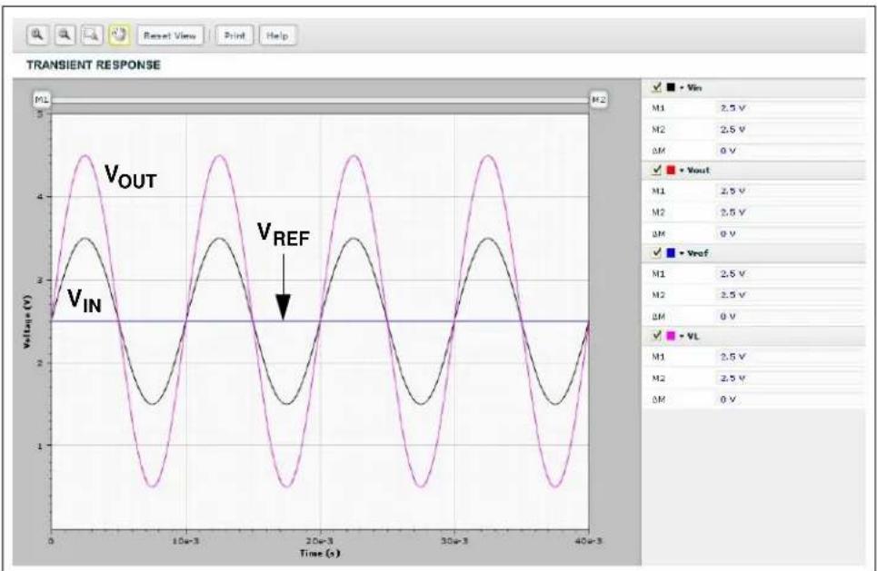
2.4.2.2.2 Sine Wave Response
In Bench Measurement:
- Se t_N is a sine wave with a frequency of 100.0 Hz, a peak-to-peak voltage of 2.0V and a center voltage of 2.5V
- The measured sine wave response is shown in Figure 2-27. It is a sine wave signal with a frequency of 100.0Hz , a peak-to-peak voltage of 4.0V and a center voltage of 2.5V
Note: The center voltage of V_IN is set at V_REF = V_DD/2 (For V_DD = 5.0V , V_REF = 2.5V )

FIGURE 2-27: Measured Sine Wave Response.
In Mindi™ Amplifier Designer:
- S e t_N is a sine wave with a frequency of 100.0 Hz, a peak-to-peak voltage of 2.0V and a center voltage of 2.5V
- The simulated sine wave response is shown in Figure 2-28. It is a sine wave signal with a frequency of 100.0Hz , a peak-to-peak voltage of 4.0V and a center voltage of 2.5V
Note: The center voltage of V_IN is set at V_REF = V_DD/2 (For V_DD = 5.0V , V_REF = 2.5V )
line
| Time (s) | V_IN (V) | V_REF (V) | |----------|----------|-----------| | 0 | ~3.0 | ~4.5 | | 10e-3 | ~1.5 | ~4.5 | | 20e-3 | ~1.5 | ~4.5 | | 30e-3 | ~1.5 | ~4.5 | | 40e-3 | ~1.5 | ~4.5 |FIGURE 2-28: Simulated Sine Wave Response.
2.4.3 Amplifier Modification: Using 8-Pin SOIC Op Amps
There are two options available when using single op amps in SOIC-8 packages (150 mil wide):
- Soldering onto the MCP6XXX Amplifier Evaluation Board 1,or
- Soldering it onto a separate board which is connected to the DIP-8 socket
Note: The DIP-8 socket must be empty; only one op amp can be used at a time.
Figure 2-29 shows a SOIC-8 op amp soldered onto the MCP6XXX Amplifier Evaluation Board 1.
text_image
CR1 JR2 R5 R6 UR1 C D VREF C2 CU2 CR2 RR2 R4 U2 CU1 U1 MICROCHIP DP1 MCP60XX Amplifier Eval Board 1 CP1 VDD GND JP1 A B C5 R7 CL RL C1 R2 C3 RISO VL GND VIN-102-00147FIGURE 2-29: Op Amp in SOIC-8 package soldered onto the MCP6XXX Amplifier Evaluation Board 1.
Figure 2-30 shows a SOIC-8 op amp and a DIP-8 socket, soldered onto the 8-Pin SOIC/MSOP/TSSOP/DIP Evaluation Board available from Microchip Technology Inc (order # SOIC8EV). The two interconnect strips on the bottom are Samtec part # BBS-14-T-B or equivalent and are soldered into the through holes for the DIP-8 socket. Figure 2-31 shows the SOIC8EV board plugged into the MCP6XXX Amplifier Evaluation Board 1.
Note: Insert the interconnect strips into the DIP-8 socket on the MCP6XXX Amplifier Evaluation Board 1. Place the SOIC8EV board on the top of the interconnect strips with the same pin orientation. Now solder the strips to the top board; this procedure ensures correct alignment of the strips. Clip the pins flush with the top surface of the SOIC8EV board, then solder the SOIC-8 op amp on the top.
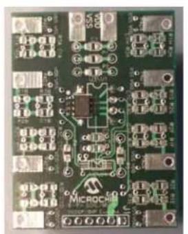
natural_image
Close-up of a green printed circuit board with various electronic components and connectors (no readable text or symbols)(Front View)
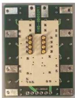
natural_image
Close-up of a green printed circuit board with gold connectors and metal contacts (no visible text or symbols)(Back View)
FIGURE 2-30: Op Amp in SOIC-8 Package Soldered onto a Separate Board.
text_image
CR1 UR1 RR1 VREF CR2 RR2 C2 R4 MICROCHIP R1 DP1 MCP6XXX Amplifier Eval Board 1 CP1 VDD GND JP1 VIN A B C5 R7 CL R2 C1 Microchip 8-Pin SDC/MOSO ISSOP/DP Evo Rd VL GND 102-00147FIGURE 2-31: Connecting Adaptor Board onto the MCP6XXX Amplifier Evaluation Board 1.
NOTES:
Appendix A. Schematic and Layouts
A.1 INTRODUCTION
This appendix contains the following schematics and layouts for the MCP6XXX Amplifier Evaluation Board 1:
- Board – Schematic
- Board – Top Silk Layer
- Board – Top Metal Layer
- Board – Bottom Metal Layer
A.2 BOARD - SCHEMATIC

text_image
A B C D Rev Description Date 1 Initial Design 3/05/07 Power Supply VS VDD DP1 6.2V CP1 1.0uF GND 1 2 3 4 5 6 7 8 9 U1 DIP8 CU1 0.1uF MCP6021-E/P R6 U2 NC 2 3 4 5 MC6021-E/SN VDD CU2 0.1uF GND JP2 C D C4 C2 R4 JP1 A VIN B R1 R2 C1 C5 R7 Output Load VL RISO CL RL Microchip MICROCHIP Filename: 103-00147-R1.sch A B C D Rev 1 3/05/07 Drawn by: J. Garcia Sheet 1 of 1A.3 BOARD - TOP SILK LAYER

text_image
CR1 JP2 R5 R6 CU1 UR1 C D RR1 C2 CU2 U1 CR2 RR2 C4 U2 R4 DP1 R1 R2 R3 MCP6XXX Amplifier C1 C3 Eval Board 1 RISO CP1 JP1 A C5 R7 CL RL B 102-00147A.4 BOARD - TOP METAL LAYER

natural_image
Pure electrical circuit lines without any symbolsA.5 BOARD - BOTTOM METAL LAYER
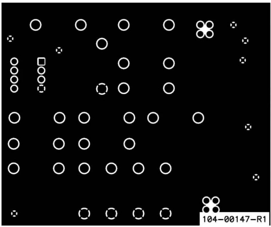
text_image
104-00147-R1NOTES:
Appendix B. Bill Of Materials (BOM)
B.1 MCP6XXX AMPLIFIER EVALUATION BOARD 1 BOM
The Bill of Materials (BOM) in Table B-1 corresponds to Figure 2-1 and Figure 2-2.
Unpopulated parts are in Table B-2.
TABLE B-1: BILL OF MATERIALS (102-00147R1) (NOTE 1)
| Qty | Reference Description Manufacturer Part Number | |||
| 1 CP1 | CAP CERAMIC 1 | UF 10% 25V X5R 0805 | Panasonic® - ECG ECJ-2F | FB1E105K |
| 4 CR1 | CR2, CU1, CU2 | CAP CERAMIC .1UF 10% 25V X7R 0805 | Panasonic - ECG ECJ-2VB | B1E104K |
| 1 DP1 | DIODE ZENER 6 | 2V 350MW SOT-23 | Fairchild Semiconductor B | ZX84C6V2 |
| 4 EA | Corner BUMPER C | LEAR .375X.15"DOME | Richco Plastic Co RBS-12 | |
| 2 J1, | J2 | CONN HEADR BRKWAY .100 04POS STR | Tyco Electronics/Amp | 9-146258-0-02 |
| 1 PCB | Ro | HS Compliant Bare PCB, MCP6XXX Amplifier Evaluation Board 1 | — | 104-00147 |
| 30 | Pin Socket | PIN RECPT .015/.025 DIA 0667 SER | Mill-Max® | 0667-0-15-01-30-27-10-0 |
| 2 RR1, | RR2 | RES 20.0K OHM 1/8W 1% 0805 SMD | Panasonic - ECG ERJ-6EN | NF2002V |
| 2 Shunts for J1&J2 | SO | CKET,SHORT BLKS W TAB BLK | JAMECO VALUEPRO | 2012JH-R |
| 6 Test Points | PC | TEST POINT COMPACT SMT | Keystone Electronics | 5016 |
| 1 UR1 | MC | P6021 SOT-23-5 Single Op Amp | Microchip Technology Inc. | MCP6021T-E/OT |
| 1 U1 | Socket CONN IC S | OCKET 8POS DIP TIN | Tyco Electronics/Amp | 2-641260-1 |
Note 1: The components listed in this Bill of Materials are representative of the PCB assembly. The released BOM used in manufacturing uses all RoHS-compliant components.
TABLE B-2: BILL OF MATERIALS – UNPOPULATED PARTS (102-00147R1)
| Qty | Reference Description Manufacturer Part Number | |||
| 1 U1 | MCP6021 PDIP-8, | Single Op Amp | Microchip Technology Inc. | MCP6021-E/P |
| 1 U2 | MCP6021 SOIC-8, | Single Op Amp | Microchip Technology Inc. | MCP6021-E/SN |
| 15 R1 | -R7, RISO, RL C1-C5, CL | Not Populated when shipped to customer | — | — |
Note 1: The components listed in this Bill of Materials are representative of the PCB assembly. The released BOM used in manufacturing uses all RoHS-compliant components.
The BOM in Table B-3 corresponds to the collection of resistors, capacitors, jumpers and MCP6021 op amps that come in the Accessory Bag which is shipped in the MCP6XXX Amplifier Evaluation Board 1 Kit. These components are placed in an separate ESD bag. They support the circuit in Section 2.4.1 "Building the Amplifier". Customers need to provide the resistors and capacitors for more amplifier circuits.
TABLE B-3: BILL OF MATERIALS – ACCESSORY BAG PARTS (102-00147R1)
| Qty | Reference Description | Manufacturer Part Number | ||
| 1 | Accessory Bag CAP C | ER 56PF 50V C0G RADIAL | Murata Electronics RPE5C | 1H560J2P1Z03B |
| 1 | Accessory Bag JUMPER | ZERO OHM 1/8W Yageo | Corporation ZOR-12 | -B-52 |
| 1 | Accessory Bag RES 97 | 6 OHM 1/4W 1% METAL FILM | Yageo Corporation | MFR-25FBF-976R |
| 1 | Accessory Bag RES 3. | 92K OHM 1/4W 1% METAL FILM | Yageo Corporation | MFR-25FBF-3K92 |
| 2 | Accessory Bag RES 1. | 96K OHM 1/4W 1% METAL FILM | Yageo Corporation | MFR-25FBF-1K96 |
| 1 | ESD Sample Box MC | P6021 Single Op Amp PDIP-8 | Microchip Technology Inc. | MCP6021-E/P |
Note 1: The components listed in this Bill of Materials are representative of the PCB assembly. The released BOM used in manufacturing uses all RoHS-compliant components.
NOTES:
WORLDWIDE SALES AND SERVICE
AMERICAS
Corporate Office
2355 West Chandler Blvd.
Chandler, AZ 85224-6199
Tel: 480-792-7200
Fax: 480-792-7277
Technical Support:
http://support.microchip.com
Web Address:
www.microchip.com
Atlanta
Duluth, GA
Tel: 678-957-9614
Fax: 678-957-1455
Boston
Westborough, MA
Tel: 774-760-0087
Fax: 774-760-0088
Chicago
Itasca, IL
Tel: 630-285-0071
Fax: 630-285-0075
Dallas
Addison, TX
Tel: 972-818-7423
Fax: 972-818-2924
Detroit
Farmington Hills, MI
Tel: 248-538-2250
Fax: 248-538-2260
Kokomo
Kokomo, IN
Tel: 765-864-8360
Fax: 765-864-8387
Los Angeles
Mission Viejo, CA
Tel: 949-462-9523
Fax: 949-462-9608
Santa Clara
Santa Clara, CA
Tel: 408-961-6444
Fax: 408-961-6445
Toronto
Mississauga, Ontario,
Canada
Tel: 905-673-0699
Fax: 905-673-6509
ASIA/PACIFIC
Asia Pacific Office
Suites 3707-14, 37th Floor
Tower 6, The Gateway
Harbour City, Kowloon
Hong Kong
Tel: 852-2401-1200
Fax: 852-2401-3431
Australia - Sydney
Tel: 61-2-9868-6733
Fax: 61-2-9868-6755
China - Beijing
Tel: 86-10-8528-2100
Fax: 86-10-8528-2104
China - Chengdu
Tel: 86-28-8665-5511
Fax: 86-28-8665-7889
China - Fuzhou
Tel: 86-591-8750-3506
Fax: 86-591-8750-3521
China - Hong Kong SAR
Tel: 852-2401-1200
Fax: 852-2401-3431
China - Qingdao
Tel: 86-532-8502-7355
Fax: 86-532-8502-7205
China - Shanghai
Tel: 86-21-5407-5533
Fax: 86-21-5407-5066
China - Shenyang
Tel: 86-24-2334-2829
Fax: 86-24-2334-2393
China - Shenzhen
Tel: 86-755-8203-2660
Fax: 86-755-8203-1760
China - Shunde
Tel: 86-757-2839-5507
Fax: 86-757-2839-5571
China - Wuhan
Tel: 86-27-5980-5300
Fax: 86-27-5980-5118
China - Xian
Tel: 86-29-8833-7252
Fax: 86-29-8833-7256
ASIA/PACIFIC
India - Bangalore
Tel: 91-80-4182-8400
Fax: 91-80-4182-8422
India - New Delhi
Tel: 91-11-4160-8631
Fax: 91-11-4160-8632
India - Pune
Tel: 91-20-2566-1512
Fax: 91-20-2566-1513
Japan - Yokohama
Tel: 81-45-471-6166
Fax: 81-45-471-6122
Korea - Daegu
Tel: 82-53-744-4301
Fax: 82-53-744-4302
Korea - Seoul
Tel: 82-2-554-7200
Fax: 82-2-558-5932 or
82-2-558-5934
Malaysia - Penang
Tel: 60-4-646-8870
Fax: 60-4-646-5086
Philippines - Manila
Tel: 63-2-634-9065
Fax: 63-2-634-9069
Singapore
Tel: 65-6334-8870
Fax: 65-6334-8850
Taiwan - Hsin Chu
Tel: 886-3-572-9526
Fax: 886-3-572-6459
Taiwan - Kaohsiung
Tel: 886-7-536-4818
Fax: 886-7-536-4803
Taiwan - Taipei
Tel: 886-2-2500-6610
Fax: 886-2-2508-0102
Thailand - Bangkok
Tel: 66-2-694-1351
Fax: 66-2-694-1350
EUROPE
Austria - Wels
Tel: 43-7242-2244-39
Fax: 43-7242-2244-393
Denmark - Copenhagen
Tel: 45-4450-2828
Fax: 45-4485-2829
France - Paris
Tel: 33-1-69-53-63-20
Fax: 33-1-69-30-90-79
Germany - Munich
Tel: 49-89-627-144-0
Fax: 49-89-627-144-44
Italy - Milan
Tel: 39-0331-742611
Fax: 39-0331-466781
Netherlands - Drunen
Tel: 31-416-690399
Fax: 31-416-690340
Spain - Madrid
Tel: 34-91-708-08-90
Fax: 34-91-708-08-91
UK - Wokingham
Tel: 44-118-921-5869
Fax: 44-118-921-5820
06/25/07