SN74LVC1GX04DCKT - Electronic component TEXAS INSTRUMENTS - Free user manual and instructions
Find the device manual for free SN74LVC1GX04DCKT TEXAS INSTRUMENTS in PDF.

User questions about SN74LVC1GX04DCKT TEXAS INSTRUMENTS
0 question about this device. Answer the ones you know or ask your own.
Ask a new question about this device
Download the instructions for your Electronic component in PDF format for free! Find your manual SN74LVC1GX04DCKT - TEXAS INSTRUMENTS and take your electronic device back in hand. On this page are published all the documents necessary for the use of your device. SN74LVC1GX04DCKT by TEXAS INSTRUMENTS.
USER MANUAL SN74LVC1GX04DCKT TEXAS INSTRUMENTS
•CrystalOscillators
- ClockGeneration
TheSN74LVC1GX04deviceisdesignedfor1.65-Vto 5.5-VV cc operation.Thisdeviceincorporates the SN74LVC1GU04(inverterwithunbufferedoutput) andtheSN74LVC1G04(inverter)functionsintoa singledevice.TheLVC1GX04isoptimizedforusein crystaloscillatorapplications.
X1 and X2 can be connected to a crystal or resonator in oscillator applications. The device provides an additional buffered inverter (Y) for signal conditioning (see Figure 5). The additional buffered inverter improves the signal quality of the crystal oscillator output by making it a trail orail.
NanoStarandNanoFree package technologyisa major breakthrough in IC packaging concepts, using thedieasthepackage.
This device is fully specified for partial-power-down applications using I_off (Y outputonly). The I_off circuitry disablestheoutputs, preventingdamagingcurrent backflow through the device when it is powered down.
DeviceInformation (1)
| PART NUMBER | PACKAGE | BODY SIZE (NOM) |
| SN74LVC1GX04DBV | SOT-23 (6) | 2.90 mm × 1.60 mm |
| SN74LVC1GX04DCK | SC70 (6) | 2.00 mm × 1.25 mm |
| SN74LVC1GX04DRL | SOT (6) | 1.60 mm × 1.20 mm |
(1) For all available packages, see the orderable addendum at the end of the data sheet.
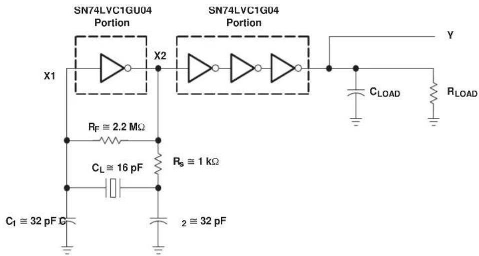
FunctionalBlockDiagram
text_image
SN74LVC1GU04 Portion X2 SN74LVC1G04 Portion Y X1 R_F ≦ 2.2 MΩ C_L ≦ 16 pF R_o ≦ 1 kΩ C_1 = 32 pF 2 = 32 pF a) Logic Diagram ViewSN74LVC1GX04 includes both dotted portions
TableofContents
1 Features.... 1
2 Applications 1
3 Description 1
4 Revision History...... 2
5PinConfigurationandFunctions....3
6 Specifications.... 4
6.1 AbsoluteMaximumRatings....4
6.2ESDRatings....4
6.3RecommendedOperatingConditions....4
6.4ThermalInformation....5
6.5 ElectricalCharacteristics....5
6.6SwitchingCharacteristics,SN74LVC1GX04....6
6.7SwitchingCharacteristics,SN74LVC1GX04....6
6.8SwitchingCharacteristics,SN74LVC1GX04......6
6.9OperatingCharacteristics....6
6.10TypicalCharacteristics....7
7ParameterMeasurementInformation......8
8DetailedDescription....10
8.1Overview....10
8.2FunctionalBlockDiagram....10
8.3FeatureDescription....10
8.4DeviceFunctionalModes....10
9ApplicationandImplementation....11
9.1 Application Information....11
9.2 Typical Application....11
10PowerSupplyRecommendations....14
11 Layout.... 15
11.1 LayoutGuidelines....15
11.2LayoutExample....15
12DeviceandDocumentationSupport....16
12.1 DocumentationSupport....16
12.2CommunityResources....16
12.3Trademarks....16
12.4ElectrostaticDischargeCaution....16
12.5Glossary....16
13Mechanical, Packaging, and Orderable Information 16
4RevisionHistory
ChangesfromRevisionC(December2013)toRevisionD
Page
- Added Pin Configuration and Functions section, ESD Ratings table, Feature Description section, Device Functional Modes, Application and Implementation section, Power Supply Recommendations section, Layout section, Device and Documentation Support section, and Mechanical, Packaging, and Orderable Information section .... 1
5PinConfigurationandFunctions
DBVPackage
6-PinSOT-23
TopView
text_image
NC 1 6 Y GND 2 5 Vcc X1 3 4 X2DCKPackage
6-PinSC70
TopView
DRLPackage
6-PinSOT
TopView

Seemechanicaldrawingsfordimensions.
NC-Nointernalconnection.
PinFunctions
| PIN | I/ODESCRIPTION | |
| NAMENO. | ||
| GND2-Ground | ||
| NC1-Nointernalconnection | ||
| VCC5-Supplypower | ||
| X13 | I Amplifierinput | |
| X24 | O Amplifieroutput | |
| Y | 6 | O Mainoutputtootherlogic |
6Specifications
6.1 AbsoluteMaximumRatings
overoperatingfree-airtemperaturerange(unlessotherwisenoted) (1)
| MINMAXUNIT | ||||
| V_CC | Supplyvoltage-0.56.5V | |||
| V_I | Inputvoltage(2) | -0.56.5V | ||
| V_O | VoltageappliedtoYoutputinthehigh-impedanceorpower-offstate(2) | -0.56.5V | ||
| V_O | Voltageappliedtoanyoutputinthehighorlowstate(2)(3) | -0.5V CC+0.5V | ||
| I_IK | InputclampcurrentV | I<0-50mA | ||
| I_OK | Outputclampcurrent | V O<0 | -50mA | |
| I_O | Continuousoutputcurrent | ±50mA | ||
| ContinuouscurrentthroughV CC orGND | ±100 | mA | ||
| T_J | Junctiontemperature | 150°C | ||
| T_stg | Storagetemperature | -65150°C | ||
(1) Stresses beyond those listed under Absolute Maximum Ratings may cause permanent damage to the device. These are stress ratings only, which do not imply functional operation of the device at these or any other conditions beyond those indicated under Recommended Operating Conditions. Exposure to absolute-maximum-rated conditions for extended periods may affect device reliability.
(2) The input and output negative-voltage ratings may be exceeded if the input and output current ratings are observed.
(3) ThevalueofV CC is provided in there recommended operating condition stable.
6.2ESDRatings
| VALUE | UNIT | |||
| V_(ESD) | Electrostatic discharge | Humanbodymodel(HBM),perAECQ100-002 (1) | ±2000 | V |
| Charged-devicemodel(CDM),perAECQ100-011 | ±1000 | |||
(1) AEC Q100-002 indicates that HBM stressing shall be in accordance with the ANSI/ESDA/JEDEC JS-001 specification.
6.3 Recommended Operating Conditions (1)
| MIN | MAX | UNIT | |||
| V_CC | Supply voltage | Operating | 1.655.5 | V | |
| Data retention only | 1.5 | ||||
| Crystaloscillatoruse | 2 | ||||
| V_IH | High-levelinputvoltage | V_CC=1.65Vto5.5V | 0.75× V_CC | V | |
| V_IL | Low-levelinputvoltage | V_CC=1.65Vto5.5V | 0.25× V_CC | V | |
| V_I | Inputvoltage | 05.5 | V | ||
| V_O | Outputvoltage | X2,Y | 0V | CC | V |
| Youtputonly,Power-downmode, V_CC=0V | 05.5 | ||||
| I_OH | High-leveloutputcurrent | V_CC=1.65V | -4 | mA | |
| V_CC=2.3V | -8 | ||||
| V_CC=3V | -16 | ||||
| -24 | |||||
| V_CC=4.5V | -32 | ||||
| I_OL | Low-leveloutputcurrent | V_CC=1.65V | 4 | mA | |
| V_CC=2.3V | 8 | ||||
| V_CC=3V | 16 | ||||
| 24 | |||||
| V_CC=4.5V | 32 | ||||
(1) AllunusedinputsofthedevicemustbeheldatV CC or GNDtoensureproperdeviceoperation. RefertotheTIapplicationreport, ImplicationsofSloworFloatingCMOSInputs, SCBA004.
RecommendedOperatingConditions (1) (continued)
| MINMAXUNIT | |||
| t/ v InputtransitionriseorfallrateV | V_CC = 1.8V ± 0.15V, 2.5V ± 0.2V20 | ||
| _CC = 3.3V ± 0.3V10ns/V | |||
| V_CC = 5V ± 0.5V10 | |||
| T_A Operatingfree-airtemperature-40125°C | |||
6.4ThermalInformation
| THERMALMETRIC (1) | SN74LVC1GX04 | UNIT | |||
| DBV(SOT-23) | DCK(SC70) | DRL(SOT) | |||
| 6PINS | 6PINS | 6PINS | |||
| R_ JA | Junction-to-ambient thermal resistance | 165 | 259 | 142 | °C/W |
(1) For more information about traditional and new thermal metrics, see the Semiconductor and IC Package Thermal Metrics application report, SPRA953.
6.5 Electrical Characteristics
over recommended operating free-air temperature range (unless otherwise noted)
| PARAMETER | TESTCONDITIONS | V_cc | MIN | TYP(1) | MAXUNIT | |||
| V_OH | I_OH=-100μA | V_I=5.5VorGND T | A=-40°Cto125°C | 1.65Vto5.5V | V_cc-0.1 | V | ||
| I_OH=-4mA | 1.65V | 1.2 | ||||||
| I_OH=-8mA | 2.3V | 1.9 | ||||||
| I_OH=-16mA | 3 V | 2.4 | ||||||
| I_OH=-24mA | 2.3 | |||||||
| I_OH=-32mA | 4.5V | 3.8 | ||||||
| V_OL | I_OL=100μA | V_I=5.5VorGND | T_A=-40°Cto125°C | 1.65Vto5.5V | 0.1 | V | ||
| I_OL=4mA | 1.65V | 0.45 | ||||||
| I_OL=8mA | 2.3V | 0.3 | ||||||
| I_OL=16mA | T_A=-40°Cto125°C | 3V | 0.4 | |||||
| I_OL=24mA | T_A=-40°Cto85°C | 3V | 0.55 | |||||
| T_A=-40°Cto125°C | 0.63 | |||||||
| I_OL=32mA | T_A=-40°Cto85°C | 4.5V | 0.55 | |||||
| T_A=-40°Cto125°C | 0.7 | |||||||
| I_I | X1 | V_I=5.5VorGND T | A=-40°C to 125°C | 0 to 5.5 V | ±5 | μA | ||
| I_off | X1,YV | I or V_O=5.5V | T_A=-40°C to 125°C | 0 | ±10 | μA | ||
| I_CC | V_I=5.5VorGND,I O=0 | T_A=-40°C to 125°C | 1.65 V to 5.5 V | 10 | μA | |||
| C_i | V_I=V_CC orGND | 3.3V | 7 | pF | ||||
(1) AlltypicalvaluesareatV CC=3.3V,T A=25°C.
6.6SwitchingCharacteristics,SN74LVC1GX04
overrecommendedoperatingfree-airtemperaturerange,C _L=15pF (unlessotherwisenoted)(seeFigure2)
| PARAMETERTE | FROMTO | cc | MINMAXUNIT | |||
| (INPUT)(OUTPUT) | ||||||
| t_pd | X1 | X2-40°Cto85°C | V_CC=1.8V±0.15V14 | ns | ||
| V_CC=2.5V±0.2V0.82.6 | ||||||
| V_CC=3.3V±0.3V0.62.4 | ||||||
| V_CC=5V±0.5V0.52 | ||||||
| Y^(1) | -40°Cto85°C | V_CC=1.8V±0.15V | 3.5 10 | |||
| V_CC=2.5V±0.2V2.26 | ||||||
| V_CC=3.3V±0.3V | 25 | |||||
| V_CC=5V±0.5V1.53.5 | ||||||
(1) X2-noexternalload
6.7 Switching Characteristics, SN74LVC1GX04
overrecommendedoperatingfree-airtemperaturerange,C =30pFor50pF(unlessotherwisenoted)(seeFigure3)
| PARAMETER | FROM(INPUT) | TO(OUTPUT) | TEMPERATURE | V_CC | MIN | MAX | UNIT |
| t_pd | X1 | X2 | -40°Cto85°C | V_CC=1.8V±0.15V | 1.1 | 7 | ns |
| V_CC=2.5V±0.2V | 0.8 | 4 | |||||
| V_CC=3.3V±0.3V | 0.8 | 3.7 | |||||
| V_CC=5V±0.5V | 0.8 | 3 | |||||
| Y^(1) | -40°Cto85°C | V_CC=1.8V±0.15V | 3.8 | 18 | |||
| V_CC=2.5V±0.2V | 2 | 7.4 | |||||
| V_CC=3.3V±0.3V | 2 | 7.8 | |||||
| V_CC=5V±0.5V | 2 | 5 |
(1) X2-noexternalload
6.8 Switching Characteristics, SN74LVC1GX04
overrecommendedoperatingfree-airtemperaturerange,C =30pFor50pF(unlessotherwisenoted)(seeFigure3)
| PARAMETER | FROM(INPUT) | TO(OUTPUT) | TEMPERATURE | V_CC | MIN | MAXUNIT |
| t_pd | X1 | X2 | -40°Cto125°C | V_CC=1.8V±0.15V | 1.1 | 8 |
| V_CC=2.5V±0.2V | 0.8 | 5 | ||||
| V_CC=3.3V±0.3V | 0.8 | 4.3 | ||||
| V_CC=5V±0.5V | 0.8 | 3.5 | ||||
| Y^(1) | -40°Cto125°C | V_CC=1.8V±0.15V | 3.8 | 20 | ||
| V_CC=2.5V±0.2V | 2 | 8.4 | ||||
| V_CC=3.3V±0.3V | 2 | 8.8 | ||||
| V_CC=5V±0.5V | 2 | 5.5 |
(1) X2-noexternalload
6.9 Operating Characteristics
T_A=25^
| PARAMETER | TEST CONDITIONS | V_CC | TYP | UNIT | |
| C_pd | Power dissipation capacitance | f = 10 MHz | V_CC= 1.8 V | 22 | pF |
| V_CC= 2.5 V | 22 | ||||
| V_CC= 3.3 V | 24 | ||||
| V_CC= 5 V | 35 | ||||
6.10 Typical Characteristics
line
| Frequency - MHz | V_CC = 5 V | V_CC = 3.3 V | V_CC = 2.7 V | V_CC = 2 V | V_CC = 1.8 V | | --------------- | ---------- | ------------ | ------------ | ---------- | ------------ | | 0.1 | 26.0 | 20.0 | 18.0 | 13.0 | 13.0 | | 1 | 26.0 | 20.0 | 18.0 | 13.0 | 13.0 | | 10 | 26.0 | 20.0 | 18.0 | 13.0 | 13.0 | | 100 | 26.0 | 20.0 | 18.0 | 13.0 | 13.0 | | >100 | ~24.0 | ~18.0 | ~14.0 | ~8.0 | ~-5.0 |Figure1.Open-LoopGainCharacteristicsofOscillatorAmplifier
7ParameterMeasurementInformation
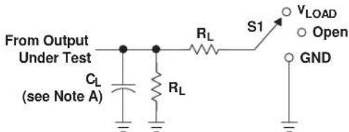
text_image
From Output Under Test CL (see Note A) RL RL S1 VLOAD Open GNDLOAD CIRCUIT
| TEST S1 | |
| p_LH/t_PHL | Open |
| p_LZ/t_PZL | V_LOAD |
| p_HZ/t_PZH | GND |
| V_CC | INPUTS | V_M | V_LOAD | C_L | R_L | V_ | |
| V_I | t_r/t_f | ||||||
| 1.8 V ± 0.15 V | V_CC | ≤2 ns | V_CC/2 | 2 · V_CC | 15 pF | 1 MΩ | 0.15 V |
| 2.5 V ± 0.2 V | V_CC | ≤2 ns | V_CC/2 | 2 · V_CC | 15 pF | 1 MΩ | 0.15 V |
| 3.3 V ± 0.3 V | 3 V | ≤2.5 ns | 1.5 V | 6 V | 15 pF | 1 MΩ | 0.3 V |
| 5 V ± 0.5 V | V_CC | ≤2.5 ns | V_CC/2 | 2 · V_CC | 15 pF | 1 MΩ | 0.3 V |
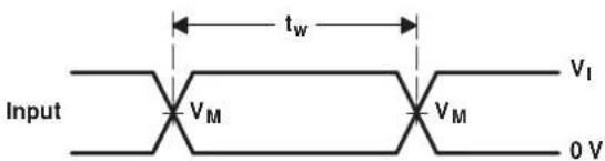
text_image
Input V_M t_W V_I V_M 0 VVOLTAGE WAVEFORMS
ENABLE AND DISABLE TIMES
LOW- AND HIGH-LEVEL ENABLING
NOTES: A. C L includes probe and jig capacitance.
B. Waveform 1 is for an output with internal conditions such that the output is low, except when disabled by the output control. Waveform 2 is for an output with internal conditions such that the output is high, except when disabled by the output control.
C. All input pulses are supplied by generators having the following characteristics: PRR ≤ 10 MHz, Z O = 50 Ω.
D. The outputs are measured one at a time, with one transition per measurement.
E. tPIZ and t_PHZ are the same as t_dis .
F. t_PZL and t_PZH are the same as t_en .
G. t_PLH and t_PHL are the same as t_pd .
H. All parameters and waveforms are not applicable to all devices.
Figure2.LoadCircuitandVoltageWaveforms
ParameterMeasurementInformation(continued)
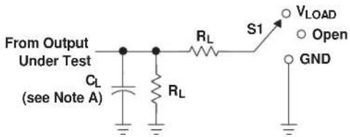
text_image
From Output Under Test CL (see Note A) RL RL S1 VLOAD Open GND| TEST S1 | |
| t_PLH/t_PHL | Open |
| t_PLZ/t_PZL | V_LOAD |
| t_PHZ/t_PZH | GND |
LOAD CIRCUIT
| V_CC | INPUTS | V_M | V_LOAD | C_L | R_L | V_ | |
| V_I | t_f/t_f | ||||||
| 1.8 V ± 0.15 V | V_CC | ≤2 ns | V_CC/2 | 2 · V_CC | 30 pF | 1 kΩ | 0.15 V |
| 2.5 V ± 0.2 V | V_CC | ≤2 ns | V_CC/2 | 2 · V_CC | 30 pF | 500 Ω | 0.15 V |
| 3.3 V ± 0.3 V | 3 V | ≤2.5 ns | 1.5 V | 6 V | 50 pF | 500 Ω | 0.3 V |
| 5 V ± 0.5 V | V_CC | ≤2.5 ns | V_CC/2 | 2 · V_CC | 50 pF | 500 Ω | 0.3 V |
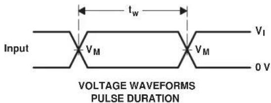
text_image
Input V_M t_w V_I V_M 0 V VOLTAGE WAVEFORMS PULSE DURATION
text_image
Timing Input V_I 0 V t_{su} t_h Data Input V_M V_M 0 V VOLTAGE WAVEFORMS SETUP AND HOLD TIMES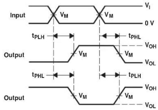
text_image
Input VM VM 0 V tPLH tPHL Output VM VM VOH VOL tPHL tPLH Output VM VM VOH VOL
text_image
Output Control V_M V_M 0 V Output Waveform 1 S1 at V_LOAD (see Note B) t_PZL V_M t_PLZ V_LOAD/2 V_OL + V_Δ V_OL t_PZH V_M t_PHZ V_OH - V_Δ V_OH ≈0 V Output Waveform 2 S1 at GND (see Note B) VOLTAGE WAVEFORMS ENABLE AND DISABLE TIMES LOW- AND HIGH-LEVEL ENABLINGVOLTAGE WAVEFORMS
PROPAGATION DELAY TIMES
INVERTING AND NONINVERTING OUTPUTS
NOTES: A. C L includes probe and jig capacitance.
B. Waveform 1 is for an output with internal conditions such that the output is low, except when disabled by the output control. Waveform 2 is for an output with internal conditions such that the output is high, except when disabled by the output control.
C. All input pulses are supplied by generators having the following characteristics: PRR ≤ 10 MHz, Z O = 50 Ω.
D. The outputs are measured one at a time, with one transition per measurement.
E. tPLZ and t_PHZ are the same as t_dis .
F. t_PZL and t_PZH are the same as t_en .
G. p_LH and t_PHL are the same as t_pd .
H. All parameters and waveforms are not applicable to all devices.
Figure3.LoadCircuitandVoltageWaveforms
8DetailedDescription
8.1Overview
TheSN74LVC1GX04isoptimizedforcreatingacrystaloscillatorcircuitwithabufferedsquare-waveoutput. This deviceisfullyspecifiedforpartial-power-downapplicationsusingI off (Youtputonly).Thel off circuitrydisablethe outputs, preventingdamagingcurrentback-flowthroughthedevicewhenitispowereddown.
8.2FunctionalBlockDiagram
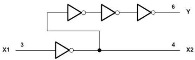
The only intended device use is to generate square-wave output using acrystal to set the operating frequency.
Table1.FunctionTable
| INPUTX1 | OUTPUTS | |
| X2 | Y | |
| HLH | ||
| LHL | ||
9ApplicationandImplementation
NOTE
InformationinthefollowingapplicationssectionsisnotpartoftheTlcomponent specification,andTldoesnotwarrantitsaccuracyorcompleteness.TI'scustomersare responsiblefordeterminingsuitabilityofcomponentsfortheirpurposes.Customersshould validateandtesttheirdesignimplementationtoconfirmsystemfunctionality.
9.1 Application Information
TheSN74LVC1GX04containsabufferedandunbufferedinverterforthespecificpurposeofcreatingacrystal oscillatoranddriverwithlimitedexternalcomponents.
9.2 Typical Application
Figure 5 shows a typical application of the SN74LVC1GX04 in a Pierce oscillator circuit. The buffered inverter (SN74LVC1G04portion) produces arail-to-rail voltage waveform. There recommended load for the crystal shown in this example is 16pF. The value of there recommended load (C can be found in the crystal manufacturer's datasheet.
ValuesofC 1 and C 2 arechosentocalculateC L in Equation1 whereC 1 ≡ G
$$ C _ {L} = \frac {C _ {1} C _ {2}}{C _ {1} + \xi} \tag {1} $$
R_s isthecurrent-limitingresistor,andthevaluedependsonthemaximumpowerdissipationofthecrystal. Generally,therecommendedvalueofR s isspecifiedinthecrystalmanufacturer'sdatasheetand,usually,this valueisapproximatelyequaltothereactanceofC 2 atresonancefrequency,thatisseeninEquation2.
$$ H _ {S} = X _ {2} \tag {2} $$
R_F isthefeedbackresistorthatisusedtobiastheinverterinthelinearregionofoperation. Usually, thevalueis chosenobewithin1MΩ to10MΩ.
text_image
SN74LVC1GU04 Portion X2 SN74LVC1G04 Portion Y X1 R_F ≈ 2.2 MΩ C_L ≈ 16 pF R_S ≈ 1 kΩ C_1 ≈ 32 pF G 2 ≈ 32 pF C_LOAD R_LOADa) Logic Diagram View
Figure5.OscillatorCircuit
TypicalApplication(continued)
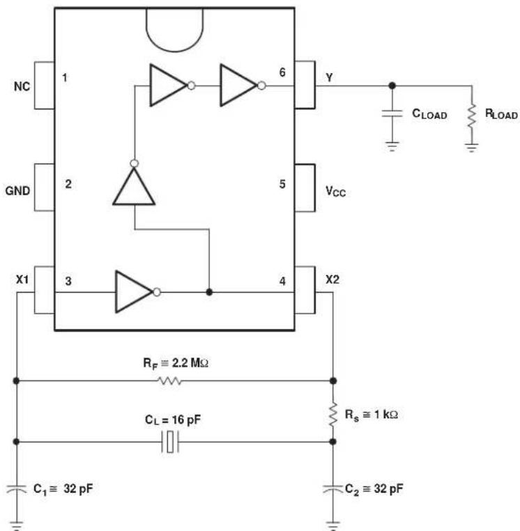
text_image
NC 1 GND 2 X1 3 6 Y VCC 5 4 X2 R_F ≡ 2.2 MΩ C_L = 16 pF C_1 ≡ 32 pF R_S ≡ 1 kΩ C_2 ≡ 32 pF C_LOAD R_LOADb) Oscillator Circuit in DBV or DCK Pinout
Figure6.OscillatorCircuit(Continued)
9.2.1 DesignRequirements
Theopen-loopgainoftheunbufferedinverterdecreasesaspower-supplyvoltagedecreases. Thisdecreasesthe closed-loopgainoftheoscillatorcircuit. ThevalueofR _s can bedecreasedtoincreasectheclosed-loopgain, while maintaining the power dissipation of the crystal within the maximum limit.
R_s and C_2 formalow-passfilterandreducespuriousoscillations. Componentvaluescanbeadjusted, based on thedesiredcutofffrequency.
C_2 can be increased over C_1 to increase the phaseshift and help start-up of the oscillator. Increasing C_2 may affect the dutycycle of the output voltage.
Athighfrequency, phaseshiftduetoR s become significant. In this case, R s can bereplaced by acapacitorto reducethephaseshift.
9.2.2 Detailed Design Procedure
Aftertheselectionofpropercomponentvalues,theoscillatorcircuitshouldbetestedusingthesecomponents. ToensurethattheoscillatorcircuitperformswithintheRecommendedOperatingConditions (1),followthese steps:
- Without acrystal, the oscillator circuit should not oscillate. To check this, the crystal can be replaced by its equivalent parallel-resonant resistance.
- Whenthepower-supplyvoltagedrops, the closed-loop gain of the oscillator circuit reduces. Ensure that the circuit oscillates at the appropriate frequency at the lowest V CC and highest V CC.
3.Ensurethatthedutycycle,start-uptime,andfrequencydriftovertimeiswithinthesystemrequirements.
(1) AllunusedinputsofthedevicemustbeheldatV CC or GNDtoensureproperdeviceoperation. RefertotheTIapplicationreport, ImplicationsofSloworFloatingCMOSInputs, SCBA004.
TypicalApplication(continued)
9.2.3ApplicationCurve
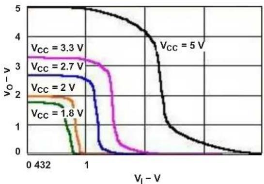
line
| V_CC (V) | V_I - V | | -------- | ------- | | 3.3 | ~0.5 | | 2.7 | ~0.6 | | 2.0 | ~0.7 | | 1.8 | ~0.8 |Figure7.V o vs V1 Characteristic of Oscillator Amplifier
10PowerSupplyRecommendations
The powersupply can be any voltage between the minimum and maximum supply voltage, ranging from (1) table.
EachV CC terminalshouldhaveagoodbypasscapacitortopreventpowerdisturbance.Fordeviceswithasingle supply,a0.1-μFcapacitorisrecommended.IftherearemultipleV CC terminalsthen0.01-μFor0.022-μF capacitorsarerecommendedforeachpowerterminal.Itisoktoparallelmultiplebypasscapacitorstoreject differentfrequenciesofnoise.Multiplebypasscapacitorsmaybeparalleledtorejectdifferentfrequenciesof noise.Thebypasscapacitorshouldbeinstalledasclosetothepowerterminalaspossibleforthebestresults.
11Layout
11.1 LayoutGuidelines
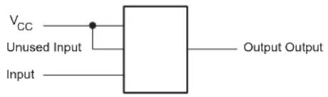
When using multiple bit logic devices, input should not float. In many cases, functions or part so function so of digital logic devices are unused. Some examples are when only two input so at triple-input AND gate are used, or when only 3 of the 4 buffer gates are used. Such input pin should not be left unconnected because the undefined voltages at the outside connections result in undefined operational states.
Specified in Figure 8 are rules that must be observed under all circumstances. All unused inputs of digital logic devices must be connected to a high or low biastoprevent them from floating. The logic level that should be applied to any particular unused input depends on the function of the device. Generally they will be tied to GND or V_CC , whichever makes moresense or is more convenient.
11.2 LayoutExample
text_image
VCC Unused Input Input Output Output
text_image
Input Unused InputFigure8.LayoutDiagram
12DeviceandDocumentationSupport
12.1 DocumentationSupport
12.1.1 RelatedDocumentation
Forrelateddocumentation,seethefollowing: ImplicationsofSloworFloatingCMOSInputs,SCBA004
12.2 Community Resources
The following links connect to TI community resources. Linked contents are provided "ASIS" by the respective contributors. They do not constitute TI specifications and do not necessarily reflect TI's views; see TI's Terms of Use.
TI E2E™ Online Community TI's Engineer-to-Engineer (E2E) Community. Created to foster collaboration amongengineers.Ate2e.ti.com,youcanaskquestions,shareknowledge,exploreideasandhelp solveproblemswithfellowengineers.
Design Support TI's Design Support Quickly find helpful E2E forums along with design support tools and contactinformationfortechnicalsupport.
12.3 Trademarks
NanoStar, NanoFree, E2EaretrademarksofTexasInstruments. Allothertrademarksarethepropertyoftheirrespectiveowners.
12.4ElectrostaticDischargeCaution

These devices have limited built-in ESD protection. The leads should be shorted together or the device placed in conductive foam duringstorageorhandlingtopreventelectrostaticdamagetotheMOSgates.
12.5Glossary
SLYZ022—TIGlossary.
This glossarylistsandexplainsterms,acronyms,anddefinitions.
13Mechanical, Packaging, and Orderable Information
The following pages include mechanical, packaging, and orderable information. This information is the most current data available for the designated devices. This data subject to changewithout notice and revision of this document. For browser-based version of this datasheet, referto the left-hand navigation.

TEXAS
INSTRUMENTS
www.ti.com
PACKAGE OPTION ADDENDUM
10-Dec-2020
PACKAGING INFORMATION
| Orderable Device Status(1) | Package Type | Package Drawing | Pins | Package Qty | Eco Plan(2) | Lead finish/ Ball material(6) | MSL Peak Temp(3) | Op Temp (°C) | Device Marking(4-5) | Samples | |
| 74LVC1GX04DCKRE4 ACTIVE SC70 DCK 6 3000 RoHS & Green NIPDAU Level-1-260C-UNLIM -40 to 125 (D25, D2J, D2K, D2 | Samples | ||||||||||
| 74LVC1GX04DCKTG4 ACTIVE SC70 DCK 6 250 RoHS & Green NIPDAU Level-1-260C-UNLIM -40 to 125 (D25, D2R) | Samples | ||||||||||
| SN74LVC1GX04DBVR | ACTIVE | SOT-23 | DBV | 6 | 3000 | RoHS & Green | NIPDAU | Level-1-260C-UNLIM | -40 to 125 | (CX45, CX4R) | Samples |
| SN74LVC1GX04DBVT ACTIVE SOT-23 DBV 6 250 RoHS & Green NIPDAU Level-1-260C-UNLIM -40 to 125 (CX45, CX4R) | Samples | ||||||||||
| SN74LVC1GX04DCKR | ACTIVE | SC70 | DCK | 6 | 3000 | RoHS & Green | NIPDAU | SN | Level-1-260C-UNLIM | -40 to 125 | (D25, D2J, D2K, D2 R) | Samples |
| SN74LVC1GX04DCKT | ACTIVE | SC70 | DCK | 6 | 250 | RoHS & Green | NIPDAU | SN | Level-1-260C-UNLIM | -40 to 125 | (D25, D2J, D2R) | Samples |
| SN74LVC1GX04DRLR | ACTIVE | SOT-5X3 | DRL | 6 | 4000 | RoHS & Green | NIPDAU | NIPDAUAG | Level-1-260C-UNLIM | -40 to 125 | (D27, D2R) | Samples |
(1) The marketing status values are defined as follows:
ACTIVE: Product device recommended for new designs.
LIFEBUY: TI has announced that the device will be discontinued, and a lifetime-buy period is in effect.
NRND: Not recommended for new designs. Device is in production to support existing customers, but TI does not recommend using this part in a new design.
PREVIEW: Device has been announced but is not in production. Samples may or may not be available.
OBSOLETE: TI has discontinued the production of the device.
(2) RoHS: TI defines "RoHS" to mean semiconductor products that are compliant with the current EU RoHS requirements for all 10 RoHS substances, including the requirement that RoHS substance do not exceed 0.1% by weight in homogeneous materials. Where designed to be soldered at high temperatures, "RoHS" products are suitable for use in specified lead-free processes. TI may reference these types of products as "Pb-Free".
RoHS Exempt: TI defines "RoHS Exempt" to mean products that contain lead but are compliant with EU RoHS pursuant to a specific EU RoHS exemption.
Green: TI defines "Green" to mean the content of Chlorine (Cl) and Bromine (Br) based flame retardants meet JS709B low halogen requirements of <=1000ppm threshold. Antimony trioxide based flame retardants must also meet the <=1000ppm threshold requirement.
(3) MSL, Peak Temp. - The Moisture Sensitivity Level rating according to the JEDEC industry standard classifications, and peak solder temperature.
(4) There may be additional marking, which relates to the logo, the lot trace code information, or the environmental category on the device.
(5) Multiple Device Markings will be inside parentheses. Only one Device Marking contained in parentheses and separated by a "\~" will appear on a device. If a line is indented then it is a continuation of the previous line and the two combined represent the entire Device Marking for that device.

TEXAS INSTRUMENTS
www.ti.com
PACKAGE OPTION ADDENDUM
10-Dec-2020
(6) Lead finish/Ball material - Orderable Devices may have multiple material finish options. Finish options are separated by a vertical ruled line. Lead finish/Ball material values may wrap to two lines if the finish value exceeds the maximum column width.
Important Information and Disclaimer: The information provided on this page represents TI's knowledge and belief as of the date that it is provided. TI bases its knowledge and belief on information provided by third parties, and makes no representation or warranty as to the accuracy of such information. Efforts are underway to better integrate information from third parties. TI has taken and continues to take reasonable steps to provide representative and accurate information but may not have conducted destructive testing or chemical analysis on incoming materials and chemicals. TI and TI suppliers consider certain information to be proprietary, and thus CAS numbers and other limited information may not be available for release.
In no event shall TI's liability arising out of such information exceed the total purchase price of the TI part(s) at issue in this document sold by TI to Customer on an annual basis.
OTHER QUALIFIED VERSIONS OF SN74LVC1GX04 :
• Enhanced Product: SN74LVC1GX04-EP
NOTE: Qualified Version Definitions:
• Enhanced Product - Supports Defense, Aerospace and Medical Applications
TAPE AND REEL INFORMATION
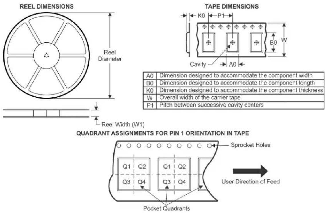
*All dimensions are nominal
| Device Package | Type | Package Drawing | Pins | SPQ Reel | Diameter (mm) | Reel Width W1 (mm) | A0 (mm) | B0 (mm) | K0 (mm) | P1 (mm) | W (mm) | Pin1 Quadrant |
| 74LVC1GX04DCKTG4 S | C70 DCK | 6 250 180 | 0 8.4 | 2.47 2.3 1.25 | 4.0 8.0 | Q3 | ||||||
| SN74LVC1GX04DBVR S | OT-23 DB | V 6 3000 | 80.0 | 8.4 3.23 3.1 | 1.37 4.0 | 8.0 Q3 | ||||||
| SN74LVC1GX04DBVR S | OT-23 DB | V 6 3000 | 78.0 | 9.2 3.3 3.23 | 1.55 4.0 | 8.0 Q3 | ||||||
| SN74LVC1GX04DBVT S | OT-23 DB | V 6 250 17 | 8.0 9.2 | 3.3 3.23 | 1.55 4.0 | 8.0 Q3 | ||||||
| SN74LVC1GX04DBVT S | OT-23 DB | V 6 250 18 | 0.0 8.4 | 3.23 3.17 | 1.37 4.0 | 8.0 Q3 | ||||||
| SN74LVC1GX04DCKR S | C70 DCK | 6 3000 | 178.0 | 9.2 2.4 2 | 4 1.22 4.0 | 8.0 Q3 | ||||||
| SN74LVC1GX04DCKR S | C70 DCK | 6 3000 | 178.0 | 9.0 2.4 2 | 5 1.2 4.0 | 8.0 Q3 | ||||||
| SN74LVC1GX04DCKR S | C70 DCK | 6 3000 | 180.0 | 8.4 2.41 | 2.41 1.2 4 | 8.0 Q3 | ||||||
| SN74LVC1GX04DCKT S | C70 | DCK 6 250 | 1 | 78.0 9.2 2 | 4 2.4 1.22 | 4.0 8.0 Q3 | ||||||
| SN74LVC1GX04DCKT S | C70 | DCK 6 250 | 1 | 80.0 8.4 2 | 41 2.41 1 | 2 4.0 8.0 Q3 | ||||||
| SN74LVC1GX04DCKT S | C70 | DCK 6 250 | 1 | 78.0 9.0 2 | 4 2.5 1.2 | 4.0 8.0 Q3 | ||||||
| SN74LVC1GX04DRLR | SOT-5X3 | DRL | 6 | 4000 | 180.0 | 8.4 | 1.98 | 1.78 | 0.69 | 4.0 | 8.0 | Q3 |
| SN74LVC1GX04DRLR | SOT-5X3 | DRL | 6 | 4000 | 180.0 | 9.5 | 1.78 | 1.78 | 0.69 | 4.0 | 8.0 | Q3 |

text_image
TAPE AND REEL BOX DIMENSIONS W L*All dimensions are nominal
| Device | Package Type | Package Drawing | Pins | SPQ | Length (mm) | Width (mm) | Height (mm) |
| 74LVC1GX04DCKTG4 SC70 DCK 6 250 183.0 | 183.0 20.0 | ||||||
| SN74LVC1GX04DBVR SOT-23 DBV 6 3000 | 202.0 201.0 | 28.0 | |||||
| SN74LVC1GX04DBVR SOT-23 DBV 6 3000 | 180.0 180.0 | 18.0 | |||||
| SN74LVC1GX04DBVT | SOT-23 DBV 6 250 180.0 | 180.0 18.0 | |||||
| SN74LVC1GX04DBVT | SOT-23 DBV 6 250 202.0 | 201.0 28.0 | |||||
| SN74LVC1GX04DCKR | SC70 DCK 6 3000 | 180.0 | 180.0 | 8.0 | |||
| SN74LVC1GX04DCKR | SC70 DCK 6 3000 | 180.0 | 180.0 | 8.0 | |||
| SN74LVC1GX04DCKR | SC70 DCK 6 3000 | 202.0 | 201.0 | 28.0 | |||
| SN74LVC1GX04DCKT SC70 DCK 6 250 180.0 | 180.0 18.0 | ||||||
| SN74LVC1GX04DCKT SC70 DCK 6 250 202.0 | 201.0 28.0 | ||||||
| SN74LVC1GX04DCKT SC70 DCK 6 250 180.0 | 180.0 18.0 | ||||||
| SN74LVC1GX04DRLR | SOT-5X3 | DRL | 6 | 4000 | 202.0 | 201.0 | 28.0 |
| SN74LVC1GX04DRLR | SOT-5X3 | DRL | 6 | 4000 | 184.0 | 184.0 | 19.0 |
DCK (R-PDSO-G6)
PLASTIC SMALL-OUTLINE PACKAGE

text_image
Pin 1 Index Area 2,15 1,85 6 4 1,40 1,10 2,40 1,80 3 1 0,65 6X 0,30 0,15 1,30 Ø 0,10 (M)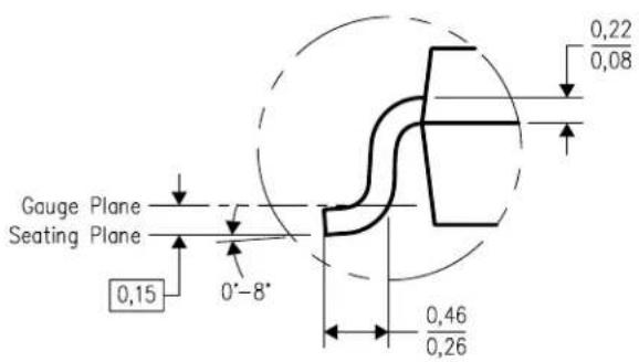
text_image
Gauge Plane Seating Plane 0,15 0°-8° 0,22 0,08 0,46 0,26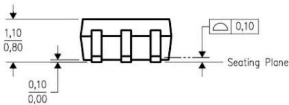
text_image
1,10 0,80 0,10 0,00 Seating Plane 0,10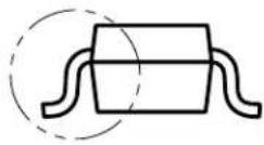
4093553-4/G 01/2007
NOTES: A. All linear dimensions are in millimeters.
B. This drawing is subject to change without notice.
C. Body dimensions do not include mold flash or protrusion. Mold flash and protrusion shall not exceed 0.15 per side.
D. Falls within JEDEC MO-203 variation AB.
DCK (R-PDSO-G6)
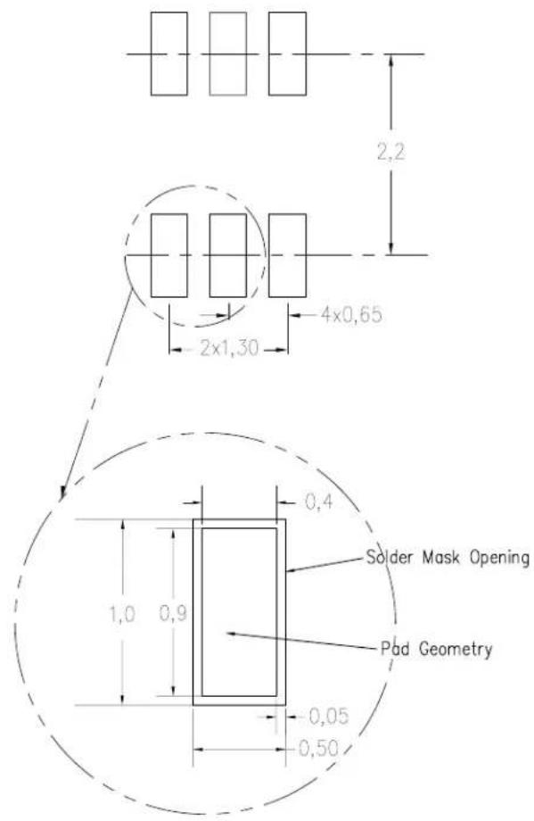
Example Board Layout
Stencil Openings
Based on a stencil thickness of .127mm (.005inch).
text_image
2,2 4x0,65 2x1,30 Solder Mask Opening 1,0 0,9 Pad Geometry 0,4 0,05 0,50
text_image
6x0,35 0,85 2,2 2x1,30 4x0,654210356-3/C 07/11
NOTES:
A. All linear dimensions are in millimeters.
B. This drawing is subject to change without notice.
C. Customers should place a note on the circuit board fabrication drawing not to alter the center solder mask defined pad.
D. Publication IPC-7351 is recommended for alternate designs.
E. Laser cutting apertures with trapezoidal walls and also rounding corners will offer better paste release. Customers should contact their board assembly site for stencil design recommendations. Example stencil design based on a 50% volumetric metal load solder paste. Refer to IPC-7525 for other stencil recommendations.
SMALL OUTLINE TRANSISTOR
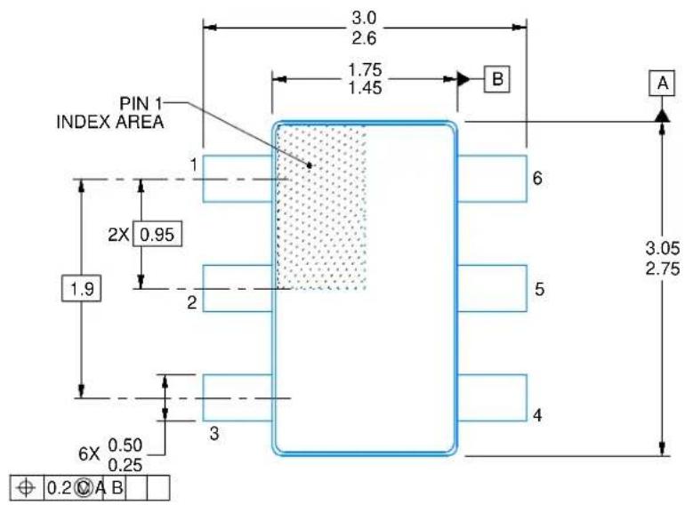
text_image
PIN 1 INDEX AREA 2X 0.95 1.9 6X 0.50 0.25 3.0 2.6 1.75 1.45 B A 6 5 4 3.05 2.75 ⊕ 0.2 @ A B
text_image
C 0.1 C 1.45 MAX (1.1) 0.15 TYP 0.00
text_image
0.25 GAGE PLANE 8° TYP 0° 0.6 TYP 0.3 0.22 TYP 0.08 SEATING PLANE4214840/C 06/2021
NOTES:
- All linear dimensions are in millimeters. Any dimensions in parenthesis are for reference only. Dimensioning and tolerancing per ASME Y14.5M.
- This drawing is subject to change without notice.
- Body dimensions do not include mold flash or protrusion. Mold flash and protrusion shall not exceed 0.25 per side.
- Leads 1,2,3 may be wider than leads 4,5,6 for package orientation.
- Reference JEDEC MO-178.
SMALL OUTLINE TRANSISTOR
text_image
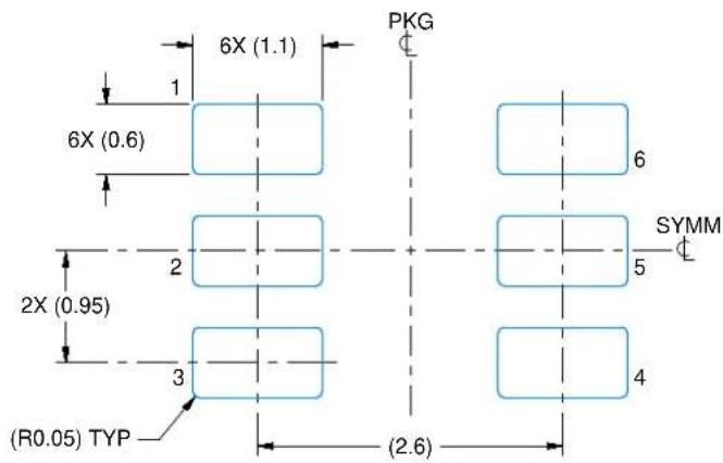
6X (1.1) PKG 1 6X (0.6) 2 2X (0.95) 3 (R0.05) TYP (2.6) SYMMLAND PATTERN EXAMPLE
EXPOSED METAL SHOWN
SCALE:15X

text_image
SOLDER MASK OPENING METAL EXPOSED METAL 0.07 MAX ARROUNDNON SOLDER MASK
DEFINED
(PREFERRED)
text_image
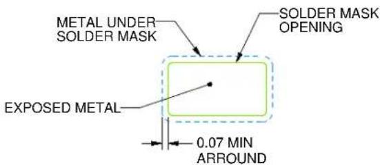
METAL UNDER SOLDER MASK SOLDER MASK OPENING EXPOSED METAL 0.07 MIN ARROUNDSOLDER MASK
DEFINED
SOLDER MASK DETAILS
4214840/C 06/2021
NOTES: (continued)
- Publication IPC-7351 may have alternate designs.
- Solder mask tolerances between and around signal pads can vary based on board fabrication site.
SMALL OUTLINE TRANSISTOR

text_image
6X (1.1) PKG 1 6X (0.6) 2 2X(0.95) 3 (R0.05) TYP (2.6) SYMM 5 4SOLDER PASTE EXAMPLE BASED ON 0.125 mm THICK STENCIL SCALE:15X
4214840/C 06/2021
NOTES: (continued)
- Laser cutting apertures with trapezoidal walls and rounded corners may offer better paste release. IPC-7525 may have alternate design recommendations.
- Board assembly site may have different recommendations for stencil design.
- All linear dimensions are in millimeters. Any dimensions in parenthesis are for reference only. Dimensioning and tolerancing per ASME Y14.5M.
- This drawing is subject to change without notice.
- This dimension does not include mold flash, protrusions, or gate burrs. Mold flash, protrusions, or gate burrs shall not exceed 0.15 mm per side.
- Reference JEDEC registration MO-293 Variation UAAD
text_image
6X (0.67) 1 6X (0.3) 4X (0.5) 3 (R0.05) TYP SYMM (1.48) (6) SYMMLAND PATTERN EXAMPLE SCALE:30X
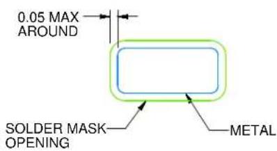
text_image
0.05 MAX AROUND SOLDER MASK OPENING METALNON SOLDER MASK DEFINED (PREFERRED)

text_image
0.05 MIN AROUND METAL UNDER SOLDER MASK SOLDER MASK OPENINGSOLDER MASK
DEFINED
SOLDERMASK DETAILS
4223266/C 12/2021
NOTES: (continued)
- Publication IPC-7351 may have alternate designs.
- Solder mask tolerances between and around signal pads can vary based on board fabrication site.
- Land pattern design aligns to IPC-610, Bottom Termination Component (BTC) solder joint inspection criteria.
text_image
6X (0.67) 1 6X (0.3) 4X (0.5) 3 (R0.05) TYP SYMM 6 SYMM 4 (1.48)SOLDER PASTE EXAMPLE BASED ON 0.1 mm THICK STENCIL SCALE:30X
4223266/C 12/2021
NOTES: (continued)
- Laser cutting apertures with trapezoidal walls and rounded corners may offer better paste release. IPC-7525 may have alternate design recommendations.
- Board assembly site may have different recommendations for stencil design.
IMPORTANT NOTICE AND DISCLAIMER
TI PROVIDES TECHNICAL AND RELIABILITY DATA (INCLUDING DATA SHEETS), DESIGN RESOURCES (INCLUDING REFERENCE DESIGNS), APPLICATION OR OTHER DESIGN ADVICE, WEB TOOLS, SAFETY INFORMATION, AND OTHER RESOURCES "AS IS" AND WITH ALL FAULTS, AND DISCLAIMS ALL WARRANTIES, EXPRESS AND IMPLIED, INCLUDING WITHOUT LIMITATION ANY IMPLIED WARRANTIES OF MERCHANTABILITY, FITNESS FOR A PARTICULAR PURPOSE OR NON-INFRINGEMENT OF THIRD PARTY INTELLECTUAL PROPERTY RIGHTS.
These resources are intended for skilled developers designing with TI products. You are solely responsible for (1) selecting the appropriate TI products for your application, (2) designing, validating and testing your application, and (3) ensuring your application meets applicable standards, and any other safety, security, regulatory or other requirements.
These resources are subject to change without notice. TI grants you permission to use these resources only for development of an application that uses the TI products described in the resource. Other reproduction and display of these resources is prohibited. No license is granted to any other TI intellectual property right or to any third party intellectual property right. TI disclaims responsibility for, and you will fully indemnify TI and its representatives against, any claims, damages, costs, losses, and liabilities arising out of your use of these resources.
TI's products are provided subject to TI's Terms of Sale or other applicable terms available either on ti.com or provided in conjunction with such TI products. TI's provision of these resources does not expand or otherwise alter TI's applicable warranties or warranty disclaimers for TI products.
TI objects to and rejects any additional or different terms you may have proposed.
Mailing Address: Texas Instruments, Post Office Box 655303, Dallas, Texas 75265
Copyright © 2022, Texas Instruments Incorporated