SN74AC373PWR - Electronic component TEXAS INSTRUMENTS - Free user manual and instructions
Find the device manual for free SN74AC373PWR TEXAS INSTRUMENTS in PDF.

User questions about SN74AC373PWR TEXAS INSTRUMENTS
0 question about this device. Answer the ones you know or ask your own.
Ask a new question about this device
Download the instructions for your Electronic component in PDF format for free! Find your manual SN74AC373PWR - TEXAS INSTRUMENTS and take your electronic device back in hand. On this page are published all the documents necessary for the use of your device. SN74AC373PWR by TEXAS INSTRUMENTS.
USER MANUAL SN74AC373PWR TEXAS INSTRUMENTS
●2-V to 6-V V cc Operation
●Inputs Accept Voltages to 6 V
●Max t pd of 9.5 ns at 5 V
●3-State Noninverting Outputs Drive Bus Lines Directly
●Full Parallel Access for Loading
description/ordering information
These 8-bit latches feature 3-state outputs designed specifically for driving highly capacitive or relatively low-impedance loads. The devices are particularly suitable for implementing buffer registers, I/O ports, bidirectional bus drivers, and working registers.
The eight latches are D-type transparent latches. When the latch-enable (LE) input is high, the Q outputs follow the data (D) inputs. When LE is taken low, the Q outputs are latched at the logic levels set up at the D inputs.
A buffered output-enable (OE) input can be used to place the eight outputs in either a normal logic state (high or low logic levels) or the high-impedance state. In the high-impedance state, the outputs neither load nor drive the bus lines significantly. The high-impedance state and increased drive provide the capability to drive bus lines in bus-organized systems without need for interface or pullup components.
SN54AC373 ... J OR W PACKAGE SN74AC373 ... DB, DW, N, NS, OR PW PACKAGE (TOP VIEW)

text_image
OE 1 20 Vcc 1Q 2 19 8Q 1D 3 18 8D 2D 4 17 7D 2Q 5 16 7Q 3Q 6 15 6Q 3D 7 14 6D 4D 8 13 5D 4Q 9 12 5Q GND 10 11 LESN54AC373 ... FK PACKAGE
(TOP VIEW)

text_image
1D 1Q OE VCC 8Q 2D 3 2 1 20 19 2Q 4 18 8D 3Q 5 17 7D 3D 6 16 7Q 4D 7 15 6Q 8 14 6D 9 10 11 12 13 4Q GND LE 5Q 5DOE does not affect the internal operations of the latches. Old data can be retained or new data can be entered while the outputs are in the high-impedance state.
ORDERING INFORMATION
| T_A | PACKAGE^† | ORDERABLEPART NUMBER | TOP-SIDEMARKING | |
| -40°C to 85°C | PDIP - N Tube SN74AC | 373N SN74AC373N | ||
| SOIC DW | Tube SN74AC373DW | AC373 | ||
| Tape and reel SN74AC373DWR | ||||
| SOP - NS Tape and reel | SN74AC373NSR AC373 | |||
| SSOP - DB Tape and reel | SN74AC373DBR AC373 | |||
| TSSOP PW | Tube SN74AC373PW | AC373 | ||
| Tape and reel SN74AC373PWR | ||||
| -55°C to 125°C | CDIP - J Tube SNJ54AC | 373J SNJ54AC373J | ||
| CFP - W | Tube SNJ54AC373W | SNJ54AC373W | ||
| LCCC - FK | Tube SNJ54AC373FK | SNJ54AC373FK | ||
^ Package drawings, standard packing quantities, thermal data, symbolization, and PCB design guidelines are available at www.ti.com/sc/package.

Please be aware that an important notice concerning availability, standard warranty, and use in critical applications of Texas Instruments semiconductor products and disclaimers thereto appears at the end of this data sheet.
description/ordering information (continued)
To ensure the high-impedance state during power up or power down, should be tied to V_CC through a pullup resistor; the minimum value of the resistor is determined by the current-sinking capability of the driver.
FUNCTION TABLE
(each latch)
| INPUTS | OUTPUTQ | |
| OE LE D | ||
| L H H H | ||
| L H L | L | |
| L L X | Q_0 | |
| H X X Z | ||
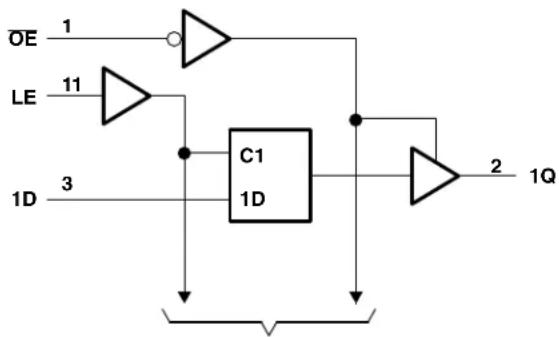
logic diagram (positive logic)
flowchart
graph TD
    OE["OE"] -->|1| NOT1["NOT"]
    LE["LE"] -->|11| NOT2["NOT"]
    1D["1D"] -->|3| NOT3["NOT"]
    NOT1 --> C1["C1"]
    NOT2 --> C1
    NOT3 --> C1
    C1 --> 1D["1D"]
    1D --> AND1["AND"]
    1D --> AND2["AND"]
    1D --> AND3["AND"]
    1D --> AND4["AND"]
    2["2"] --> AND5["AND"]
    1Q["1Q"] --> AND5
    1Q --> AND6["AND"]
To Seven Other Channels
absolute maximum ratings over operating free-air temperature range (unless otherwise noted) ^†
Supply voltage range, V_CC -0.5 V to 7 V
Input voltage range, V_I (see Note 1) -0.5 V. to V. CC + 0.5 V
Output voltage range, V_O (see Note 1) -0.5 V to V_CC + 0.5 V
Input clamp current, I_IK ( V_I < 0 or V_I > V_CC ) .... ± 20 mA
Output clamp current, I_OK ( V_O < 0 or V_O > V_CC ) ±20 mA
Continuous output current, I_O ( V_O = 0 to V_CC ) ± 50 mA
Continuous current through V_CC or GND ± 200 mA
Package thermal impedance, _JA (see Note 2): DB package 70^ / W
DW package 58°C/W
N package 69°C/W
NS package 60°C/W
PW package 83°C/W
Storage temperature range, T_stg -65^ to 150^
^ Stresses beyond those listed under “absolute maximum ratings” may cause permanent damage to the device. These are stress ratings only, and functional operation of the device at these or any other conditions beyond those indicated under “recommended operating conditions” is not implied. Exposure to absolute-maximum-rated conditions for extended periods may affect device reliability.
NOTES: 1. The input and output voltage ratings may be exceeded if the input and output current ratings are observed.
- The package thermal impedance is calculated in accordance with JESD 51-7.
recommended operating conditions (see Note 3)
| SN54AC373 S | N74AC373 | UNIT | ||
| MIN MAX MIN | MAX | |||
| V_CC Supply voltage 2 6 2 6 V | ||||
| V_iHI High-level input voltage | V_CC=3 V 2.1 2.1 | V | ||
| V_CC=4.5 V 3.15 3.15 | ||||
| V_CC=5.5 V 3.85 3.85 | ||||
| V_iL Low-level input voltage | V_CC=3 V 0.9 0.9 | V | ||
| V_CC=4.5 V 1.35 1.35 | ||||
| V_CC=5.5 V 1.65 1.65 | ||||
| V_I Input voltage | 0 V CC | 0 V_CC | V | |
| V_O Output voltage | 0 V CC | 0 V_CC | V | |
| I_QH High-level output current | V_CC=3 V | -12 | -12 | mA |
| V_CC=4.5 V -24 | -24 | |||
| V_CC=5.5 V -24 | -24 | |||
| I_OL Low-level output current | V_CC=3 V | 12 | 12 | mA |
| V_CC=4.5 V | 24 | 24 | ||
| V_CC=5.5 V | 24 | 24 | ||
| t/ v Input transition rise or fall rate | 8 | 8 | ns/V | |
| T_A Operating free-air temperature | -55 125 | -40 85 | °C | |
NOTE 3: All unused inputs of the device must be held at V_CC or GND to ensure proper device operation. Refer to the TI application report, Implications of Slow or Floating CMOS Inputs, literature number SCBA004.
electrical characteristics over recommended operating free-air temperature range (unless otherwise noted)
| PARAMETER | TEST CONDITIONS | V_CC | T_A=25°C | SN54AC373 SN74AC373 | UNIT | ||
| MIN | TYP MAX MIN | MAX MIN MAX | |||||
| V_OH | I_QHI=-50μA | 3 V | 2.9 | 2.9 | 2.9 | V | |
| 4.5 V | 4.4 | 4.4 | 4.4 | ||||
| 5.5 V | 5.4 | 5.4 | 5.4 | ||||
| I_OH=-12mA | 3 V | 2.56 | 2.4 | 2.46 | |||
| I_OH=-24mA | 4.5 V | 3.86 | 3.7 | 3.76 | |||
| 5.5 V | 4.86 | 4.7 | 4.76 | ||||
| V_OL | I_OL=50μA | 3 V | 0.1 | 0.1 | 0.1 | V | |
| 4.5 V | 0.1 | 0.1 | 0.1 | ||||
| 5.5 V | 0.1 | 0.1 | 0.1 | ||||
| I_OL=12mA | 3 V | 0.36 | 0.5 | 0.44 | |||
| I_OL=24mA | 4.5 V 0.36 | 0.5 | 0.44 | ||||
| 5.5 V 0.36 | 0.5 | 0.44 | |||||
| I_I | V_I=V_CC or GND | 5.5 V | ±0.1 | ±1 | ±1 | μA | |
| I_OZ | V_O=V_CC or GND | 5.5 V | ±0.25 | ±5 | ±2.5 | μA | |
| I_CC | V_I=V_CC or GND, I O=0 | 5.5 V | 4 | 80 | 40 | μA | |
| C_i | V_I=V_CC or GND | 5 V | 4.5 | pF | |||
timing requirements over recommended operating free-air temperature range, V_CC = 3.3 V ± 0.3 V (unless otherwise noted) (see Figure 1)
| T_A = 25^ CSN | 54AC373 SN74AC373 | UNIT | |||
| MIN MAX MIN | MAX MIN MAX | ||||
| t_w | Pulse duration, LE high 5.5 6.5 6 ns | ||||
| t_su | Setup time, data before LE↓ 5.5 6.5 6 ns | ||||
| t_h | Hold time, data after LE↓ 1 1 1 ns | ||||
timing requirements over recommended operating free-air temperature range, V_CC = 5 V ± 0.5 V (unless otherwise noted) (see Figure 1)
| T_A=25°C SN | 54AC373 SN74AC373 | UNIT | |||
| MIN MAX MIN | MAX MIN MAX | ||||
| t_w | Pulse duration, LE high 4 5 4.5 ns | ||||
| t_su | Setup time, data before LE↓ | 4 | 5 | 4.5 | ns |
| t_h | Hold time, data after LE↓ | 1 | 1 | 1 | ns |
switching characteristics over recommended operating free-air temperature range, V_CC = 3.3 V ± 0.3 V (unless otherwise noted) (see Figure 1)
| PARAMETER | TO(INPUT) | TO(OUTPUT) | T_A=25°C | SN54AC373 SN74AC373 | UNIT | |||||
| MIN | TYP | MAX MIN | MAX | MIN | MAX | |||||
| t_PLH | D | Q | 1.5 | 10 | 13.5 | 1 | 16.5 | 1.5 | 15 | ns |
| t_PHL | 1.5 | 9.5 | 13.0 | 1 | 16 | 1.5 | 14.5 | |||
| t_PLH | LE | Q | 1.5 | 10 | 13.5 | 1 | 16.5 | 1.5 | 15 | ns |
| t_PHL | 1.5 | 9.5 | 12.5 | 1 | 15 | 1.5 | 14 | |||
| t_PZH | Q | 1.5 | 9 | 11.5 | 1 | 14 | 1 | 13 | ns | |
| t_PZL | 1.5 | 8.5 | 11.5 | 1 | 13.5 | 1 | 13 | |||
| t_PHZ | Q | 1.5 | 10 | 12.5 | 1 | 16 | 1 | 14.5 | ns | |
| t_PLZ | 1.5 | 8 | 11.5 | 1 | 13 | 1 | 12.5 | |||
switching characteristics over recommended operating free-air temperature range, V_CC = 5 V ± 0.5 V (unless otherwise noted) (see Figure 1)
| PARAMETER | TO(INPUT) | TO(OUTPUT) | T_A = 25°C | SN54AC373 SN74AC373 | UNIT | |||||
| MIN | TYP MAX MIN | MAX MIN MAX | ||||||||
| t_PLH | D | Q | 1.5 | 7 | 9.5 | 1 | 11.5 | 1.5 | 10.5 | ns |
| t_PHL | 1.5 | 7 | 9.5 | 1 | 11.5 | 1.5 | 10.5 | |||
| t_PLH | LE | Q | 1.5 | 7.5 | 9.5 | 1 | 12 | 1.5 | 10.5 | ns |
| t_PHL | 1.5 | 7 | 9.5 | 1 | 11 | 1.5 | 10.5 | |||
| t_PZH | Q | 1.5 | 7 | 8.5 | 1 | 10.5 | 1 | 9.5 | ns | |
| t_PZL | 1.5 | 6.5 | 8.5 | 1 | 10 | 1 | 9.5 | |||
| t_PHZ | Q | 1.5 | 8 | 11 | 1 | 13.5 | 1 | 12.5 | ns | |
| t_PLZ | 1.5 | 6.5 | 8.5 | 1 | 10.5 | 1 | 10 | |||
operating characteristics, V_CC = 5 V , T_A = 25^
| PARAMETER | TEST CONDITIONS | TYP | UNIT | |
| C_pd | Power dissipation capacitance | C_L = 50 pF, f = 1 MHz | 40 | pF |
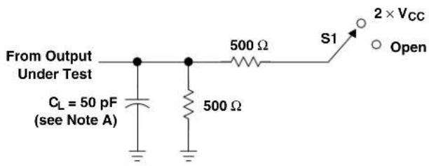
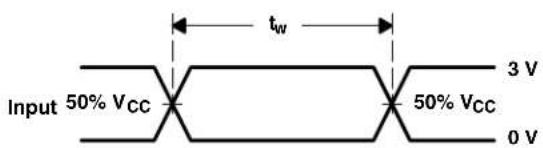
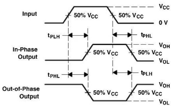
PARAMETER MEASUREMENT INFORMATION
text_image
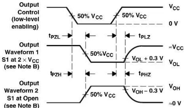
From Output Under Test C_L = 50 pF (see Note A) 500 Ω 500 Ω S1 2 × V_CC OpenLOAD CIRCUIT
| TEST S1 | |
| t_PLH/t_PHL | Open |
| t_PLZ/t_PZL | 2 × V_CC |
| t_PHZ/t_PZH | Open |
text_image
Input 50% Vcc tw 50% Vcc 3 V 0 VVOLTAGE WAVEFORMS

text_image
Timing Input 50% VCC VCC 0 V tsu th Data Input 50% VCC 50% VCC VCC 0 VVOLTAGE WAVEFORMS
text_image
Input 50% VCC 50% VCC VCC 0 V tPLH tPHL In-Phase Output 50% VCC 50% VCC VOH VOL tPHL tPLH Out-of-Phase Output 50% VCC 50% VCC VOH VOLVOLTAGE WAVEFORMS
other
| Signal Type | Condition | Voltage Level | Time to Output | |-------------|-----------|---------------|----------------| | Output Waveform 1 | Low-level enabling | VCC | 0 V | | Output Waveform 1 | S1 at 2 × VCC (see Note B) | VCC | =VCC | | Output Waveform 1 | S1 at 2 × VCC (see Note B) | VOL + 0.3 V | VOL | | Output Waveform 1 | S1 at 2 × VCC (see Note B) | VOL - 0.3 V | VOL | | Output Waveform 2 | S1 at Open (see Note B) | VCC | =0 V | | Output Waveform 2 | S1 at Open (see Note B) | VOL - 0.3 V | VOL |VOLTAGE WAVEFORMS
NOTES: A. C L includes probe and jig capacitance.
B. Waveform 1 is for an output with internal conditions such that the output is low except when disabled by the output control. Waveform 2 is for an output with internal conditions such that the output is high except when disabled by the output control.
C. All input pulses are supplied by generators having the following characteristics: PRR ≤ 1 MHz, Z O = 50 Ω, t r ≤ 2.5 ns, t _f ≤ 2.5 ns.
D. The outputs are measured one at a time with one input transition per measurement.
Figure 1. Load Circuit and Voltage Waveforms
PACKAGING INFORMATION
| Orderable Device Status(1) | Package Type Package Drawing | Pins | Package Qty | Eco Plan(2) | Lead finish/ Ball material(6) | MSL Peak Temp(3) | Op Temp (°C) | Device Marking(4/5) | Samples | |
| 5962-87555012A ACTIVE LCCC FK 20 1 Non-RoHS | & Green | SNPB N / A for Pkg Type -55 to 125 5962- | 87555012ASNJ54AC373FK | Samples | ||||||
| 5962-8755501RA ACTIVE CDIP J 20 1 Non-RoHS | & Green | SNPB N / A for Pkg Type -55 to 125 5962-8755501RA | SNJ54AC373J | Samples | ||||||
| 5962-8755501SA ACTIVE CFP W 20 1 Non-RoHS | & Green | SNPB N / A for Pkg Type -55 to 125 5962-8755501SA | SNJ54AC373W | Samples | ||||||
| 5962-8755501VSA ACTIVE CFP | W 20 25 Non-RoHS | & Green | SNPB N / A for Pkg Type -55 to 125 5962-8755501VS | ASNV54AC373W | Samples | |||||
| SN74AC373DBR | ACTIVE | SSOP | DB | 20 | 2000 | RoHS & Green | NIPDAU | Level-1-260C-UNLIM | -40 to 85 | AC373 |
| SN74AC373DW | ACTIVE | SOIC | DW | 20 | 25 | RoHS & Green | NIPDAU | Level-1-260C-UNLIM | -40 to 85 | AC373 |
| SN74AC373DWR | ACTIVE | SOIC | DW | 20 | 2000 | RoHS & Green | NIPDAU | Level-1-260C-UNLIM | -40 to 85 | AC373 |
| SN74AC373DWRE4 | ACTIVE | SOIC | DW | 20 | 2000 | RoHS & Green | NIPDAU | Level-1-260C-UNLIM | -40 to 85 | AC373 |
| SN74AC373N | ACTIVE | PDIP | N | 20 | 20 | RoHS & Green | NIPDAU | N / A for Pkg Type | -40 to 85 | SN74AC373N |
| SN74AC373NE4 | ACTIVE | PDIP | N | 20 | 20 | RoHS & Green | NIPDAU | N / A for Pkg Type | -40 to 85 | SN74AC373N |
| SN74AC373NSR | ACTIVE | SO | NS | 20 | 2000 | RoHS & Green | NIPDAU | Level-1-260C-UNLIM | -40 to 85 | AC373 |
| SN74AC373PW | ACTIVE | TSSOP | PW | 20 | 70 | RoHS & Green | NIPDAU | Level-1-260C-UNLIM | -40 to 85 | AC373 |
| SN74AC373PWR | ACTIVE | TSSOP | PW | 20 | 2000 | RoHS & Green | NIPDAU | Level-1-260C-UNLIM | -40 to 85 | AC373 |
| SNJ54AC373FK | ACTIVE LCCC FK 20 1 Non-RoHS | & Green | SNPB N / A for Pkg Type -55 to 125 5962- | 87555012ASNJ54AC373FK | Samples | |||||
| SNJ54AC373J | ACTIVE CDIP J 20 1 Non-RoHS | & Green | SNPB N / A for Pkg Type -55 to 125 5962-8755501RA | SNJ54AC373J | Samples | |||||
| SNJ54AC373W | ACTIVE CFP | W 20 1 Non-RoHS | & Green | SNPB N / A for Pkg Type -55 to 125 5962-8755501SA | SNJ54AC373W | Samples | ||||

TEXAS
INSTRUMENTS
www.ti.com
PACKAGE OPTION ADDENDUM
24-Sep-2021
(1) The marketing status values are defined as follows:
ACTIVE: Product device recommended for new designs.
LIFEBUY: TI has announced that the device will be discontinued, and a lifetime-buy period is in effect.
NRND: Not recommended for new designs. Device is in production to support existing customers, but TI does not recommend using this part in a new design.
PREVIEW: Device has been announced but is not in production. Samples may or may not be available.
OBSOLETE: TI has discontinued the production of the device.
^(2) RoHS: TI defines "RoHS" to mean semiconductor products that are compliant with the current EU RoHS requirements for all 10 RoHS substances, including the requirement that RoHS substance do not exceed 0.1% by weight in homogeneous materials. Where designed to be soldered at high temperatures, "RoHS" products are suitable for use in specified lead-free processes. TI may reference these types of products as "Pb-Free".
RoHS Exempt: TI defines "RoHS Exempt" to mean products that contain lead but are compliant with EU RoHS pursuant to a specific EU RoHS exemption.
Green: TI defines "Green" to mean the content of Chlorine (Cl) and Bromine (Br) based flame retardants meet JS709B low halogen requirements of <=1000ppm threshold. Antimony trioxide based flame retardants must also meet the <=1000ppm threshold requirement.
(3) MSL, Peak Temp. - The Moisture Sensitivity Level rating according to the JEDEC industry standard classifications, and peak solder temperature.
(4) There may be additional marking, which relates to the logo, the lot trace code information, or the environmental category on the device.
(5) Multiple Device Markings will be inside parentheses. Only one Device Marking contained in parentheses and separated by a "\~" will appear on a device. If a line is indented then it is a continuation of the previous line and the two combined represent the entire Device Marking for that device.
(6) Lead finish/Ball material - Orderable Devices may have multiple material finish options. Finish options are separated by a vertical ruled line. Lead finish/Ball material values may wrap to two lines if the finish value exceeds the maximum column width.
Important Information and Disclaimer: The information provided on this page represents TI's knowledge and belief as of the date that it is provided. TI bases its knowledge and belief on information provided by third parties, and makes no representation or warranty as to the accuracy of such information. Efforts are underway to better integrate information from third parties. TI has taken and continues to take reasonable steps to provide representative and accurate information but may not have conducted destructive testing or chemical analysis on incoming materials and chemicals. TI and TI suppliers consider certain information to be proprietary, and thus CAS numbers and other limited information may not be available for release.
In no event shall TI's liability arising out of such information exceed the total purchase price of the TI part(s) at issue in this document sold by TI to Customer on an annual basis.
OTHER QUALIFIED VERSIONS OF SN54AC373, SN54AC373-SP, SN74AC373 :
• Catalog : SN74AC373, SN54AC373
• Enhanced Product : SN74AC373-EP, SN74AC373-EP
• Military : SN54AC373
• Space : SN54AC373-SP
NOTE: Qualified Version Definitions:
• Catalog - TI's standard catalog product
• Enhanced Product - Supports Defense, Aerospace and Medical Applications
• Military - QML certified for Military and Defense Applications
• Space - Radiation tolerant, ceramic packaging and qualified for use in Space-based application
TAPE AND REEL INFORMATION
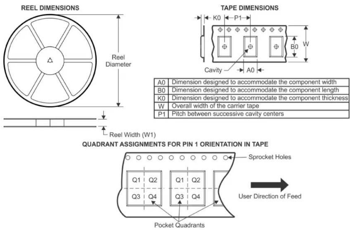
*All dimensions are nominal
| Device Package | Type | Package Drawing | Pins | SPQ Reel | Diameter (mm) | Reel Width W1 (mm) | A0 (mm) | B0 (mm) | K0 (mm) | P1 (mm) | W (mm) | Pin1 Quadrant |
| SN74AC373DBR SSO | P DB 20 2 | 000 330.0 | 16.4 8 | 2.7 5 2.5 | 12.0 16.0 | Q1 | ||||||
| SN74AC373DWR SOI | C DW 20 | 2000 330.0 | 24.4 | 0.8 13.3 2 | 7 12.0 24 | 0 Q1 | ||||||
| SN74AC373NSR SO | NS 20 2000 | 330.0 24 | 4 8.4 | 13.0 2.5 1 | 2.0 24.0 | Q1 | ||||||
| SN74AC373PWR TSS | OP PW 20 | 2000 330 | 0 16.4 | 6.95 7.0 | 1.4 8.0 16.0 | Q1 |
text_image
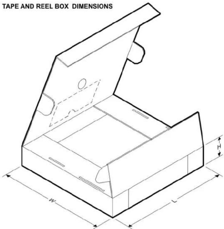
TAPE AND REEL BOX DIMENSIONS W L*All dimensions are nominal
| Device | Package Type | Package Drawing | Pins | SPQ | Length (mm) | Width (mm) | Height (mm) |
| SN74AC373DBR SSOP | DB 20 2000 853.0 | 449.0 35.0 | |||||
| SN74AC373DWR SOIC | DW 20 2000 367.0 | 367.0 45.0 | |||||
| SN74AC373NSR SO | NS 20 2000 367.0 | 367.0 45.0 | |||||
| SN74AC373PWR | TSSOP | PW | 20 | 2000 | 853.0 | 449.0 | 35.0 |
TUBE

text_image
T - Tube height W-Tube width L - Tube length B - Alignment groove width*All dimensions are nominal
| Device | Package Name | Package Type | Pins | SPQ | L (mm) | W (mm) | T (μm) | B (mm) |
| 5962-87555012A FK LCCC 20 1 506.98 12.06 2030 NA | ||||||||
| 5962-8755501VSA W CFP 20 | 25 506.98 | 26.16 6220 | NA | |||||
| SN74AC373DW | DW | SOIC | 20 | 25 | 507 | 12.83 | 5080 | 6.6 |
| SN74AC373N | N | PDIP | 20 | 20 | 506 | 13.97 | 11230 | 4.32 |
| SN74AC373NE4 | N | PDIP | 20 | 20 | 506 | 13.97 | 11230 | 4.32 |
| SN74AC373PW | PW | TSSOP | 20 | 70 | 530 | 10.2 | 3600 | 3.5 |
| SNJ54AC373FK | FK LCCC 20 1 506.98 12.06 2030 NA | |||||||
W (R-GDFP-F20)
CERAMIC DUAL FLATPACK
NOTES: A. All linear dimensions are in inches (millimeters).
B. This drawing is subject to change without notice.
C. This package can be hermetically sealed with a ceramic lid using glass frit.
D. Index point is provided on cap for terminal identification only.
E. Falls within Mil-Std 1835 GDFP2-F20
SMALL OUTLINE PACKAGE
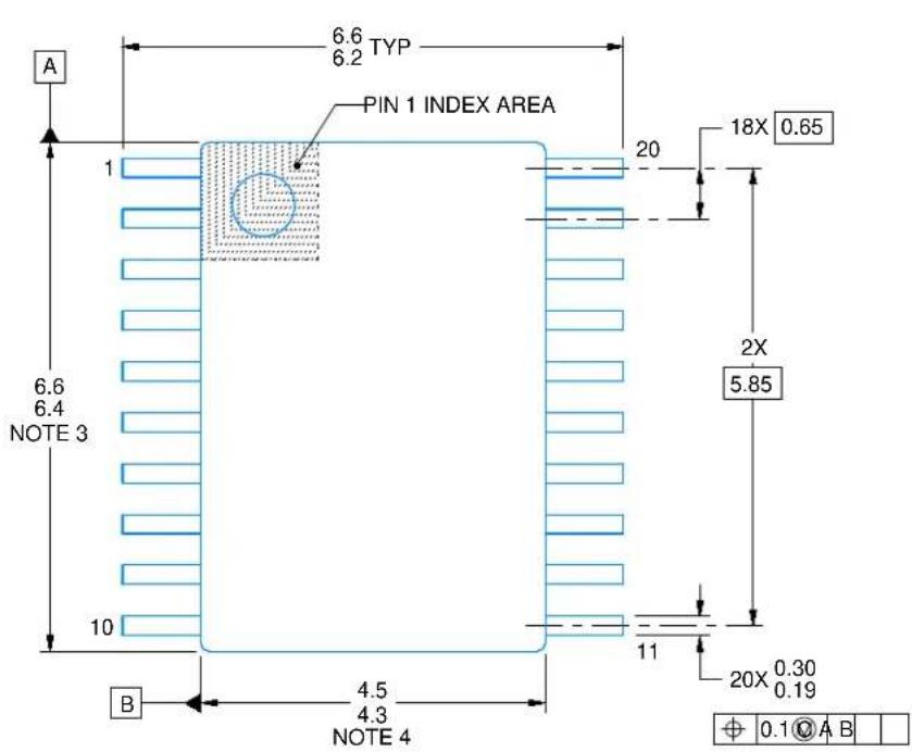
text_image
A 6.6 TYP 6.2 PIN 1 INDEX AREA 1 20 18X 0.65 6.6 6.4 NOTE 3 2X 5.85 10 11 20X 0.30 0.19 B 4.5 4.3 NOTE 4 ⊕ 0.1@ A B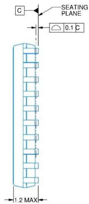
text_image
C SEATING PLANE 0.1 C 1.2 MAX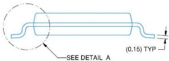
text_image
SEE DETAIL A (0.15) TYP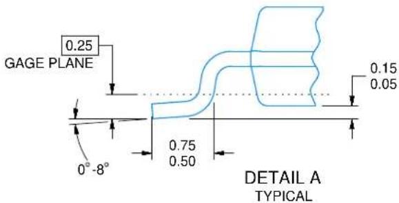
text_image
GAGE PLANE 0.25 0.15 0.05 0° -8° 0.75 0.50 DETAIL A TYPICAL4220206/A 02/2017
NOTES:
- All linear dimensions are in millimeters. Any dimensions in parenthesis are for reference only. Dimensioning and tolerancing per ASME Y14.5M.
- This drawing is subject to change without notice.
- This dimension does not include mold flash, protrusions, or gate burrs. Mold flash, protrusions, or gate burrs shall not exceed 0.15 mm per side.
- This dimension does not include interlead flash. Interlead flash shall not exceed 0.25 mm per side.
- Reference JEDEC registration MO-153.
SMALL OUTLINE PACKAGE
text_image
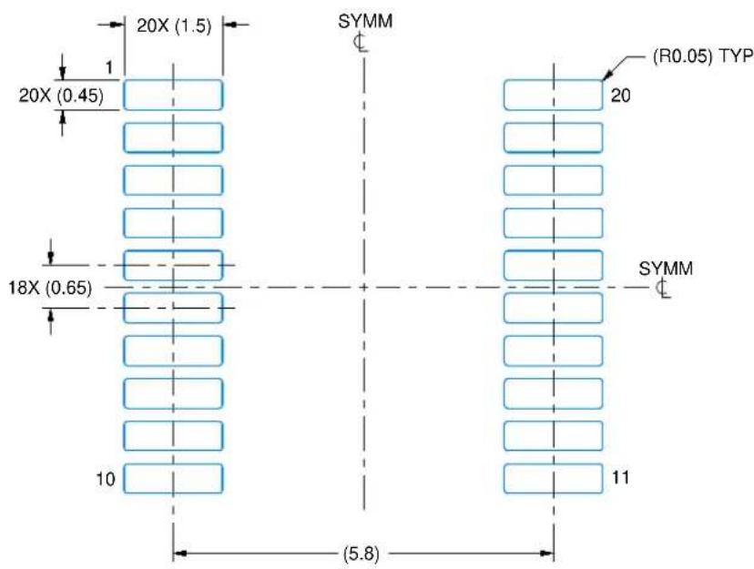
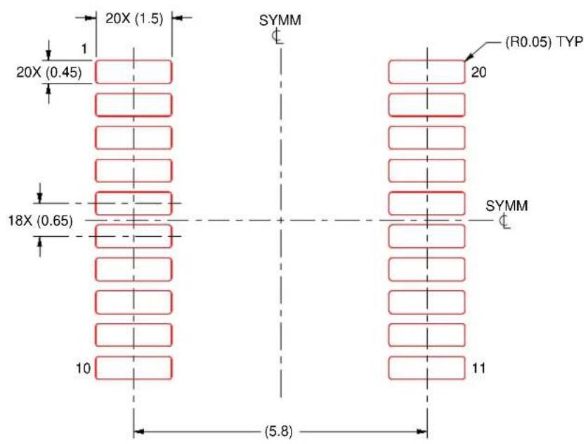
20X (1.5) 1 20X (0.45) SYMM (R0.05) TYP 18X (0.65) 10 (5.8) 11 SYMMLAND PATTERN EXAMPLE
EXPOSED METAL SHOWN
SCALE: 10X
text_image
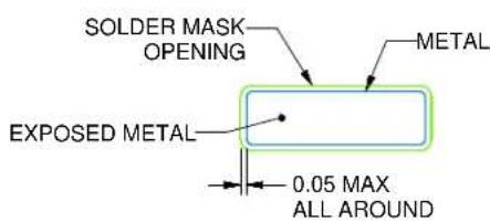
SOLDER MASK OPENING METAL EXPOSED METAL 0.05 MAX ALL AROUNDNON-SOLDER MASK DEFINED (PREFERRED)
text_image
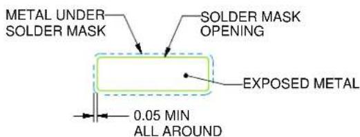
METAL UNDER SOLDER MASK SOLDER MASK OPENING EXPOSED METAL 0.05 MIN ALL AROUNDSOLDER MASK DETAILS
4220206/A 02/2017
NOTES: (continued)
- Publication IPC-7351 may have alternate designs.
- Solder mask tolerances between and around signal pads can vary based on board fabrication site.
SMALL OUTLINE PACKAGE
text_image
20X (1.5) 1 20X (0.45) 18X (0.65) 10 (5.8) SYMM (20) (R0.05) TYP SYMM 11SOLDER PASTE EXAMPLE
BASED ON 0.125 mm THICK STENCIL
SCALE: 10X
4220206/A 02/2017
NOTES: (continued)
- Laser cutting apertures with trapezoidal walls and rounded corners may offer better paste release. IPC-7525 may have alternate design recommendations.
- Board assembly site may have different recommendations for stencil design.
PW (R-PDSO-G20)
Example Board Layout

text_image
18x0,65 5,6 Example Non Soldermask Defined Pad Example Solder Mask Opening (See Note E) 0,3 1,6 0,07 Pad Geometry All AroundBased on a stencil thickness of .127mm (.005inch).
text_image
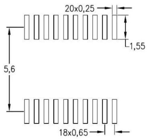
20x0,25 1,55 5,6 18x0,654211284-5/G 08/15
NOTES:
A. All linear dimensions are in millimeters.
B. This drawing is subject to change without notice.
C. Publication IPC-7351 is recommended for alternate design.
D. Laser cutting apertures with trapezoidal walls and also rounding corners will offer better paste release. Customers should contact their board assembly site for stencil design recommendations. Refer to IPC-7525 for other stencil recommendations.
E. Customers should contact their board fabrication site for solder mask tolerances between and around signal pads.
FK (S-CQCC-N**)
28 TERMINAL SHOWN
LEADLESS CERAMIC CHIP CARRIER
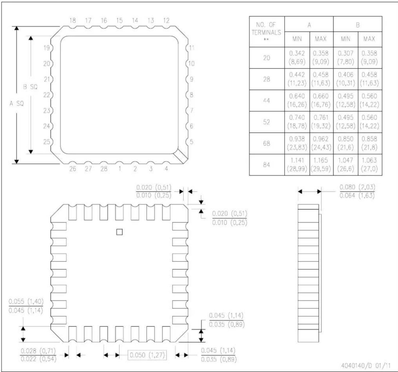
| NO. OF TERMINALS** | A | B | ||
| MIN | MAX | MIN | MAX | |
| 20 | 0.342(8,69) | 0.358(9,09) | 0.307(7,80) | 0.358(9,09) |
| 28 | 0.442(11,23) | 0.458(11,63) | 0.406(10,31) | 0.458(11,63) |
| 44 | 0.640(16,26) | 0.660(16,76) | 0.495(12,58) | 0.560(14,22) |
| 52 | 0.740(18,78) | 0.761(19,32) | 0.495(12,58) | 0.560(14,22) |
| 68 | 0.938(23,83) | 0.962(24,43) | 0.850(21,6) | 0.858(21,8) |
| 84 | 1.141(28,99) | 1.165(29,59) | 1.047(26,6) | 1.063(27,0) |
4040140/D 01/11
NOTES: A. All linear dimensions are in inches (millimeters).
B. This drawing is subject to change without notice.
C. This package can be hermetically sealed with a metal lid.
D. Falls within JEDEC MS-004
SMALL OUTLINE PACKAGE

text_image
A 8.2 7.4 TYP PIN 1 INDEX AREA 1 20 18X 0.65 7.5 6.9 NOTE 3 2X 5.85 10 11 20X 0.38 0.22 B 5.6 5.0 NOTE 4 ⊕ 0.1@ A B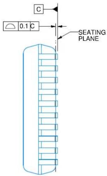
text_image
C 0.1 C SEATING PLANE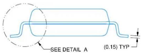
text_image
SEE DETAIL A (0.15) TYP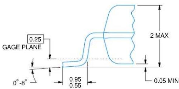
text_image
GAGE PLANE 0.25 0° -8° 0.95 0.55 2 MAX 0.05 MINDETAIL A TYPICAL
4214851/B 08/2019
NOTES:
- All linear dimensions are in millimeters. Any dimensions in parenthesis are for reference only. Dimensioning and tolerancing per ASME Y14.5M.
- This drawing is subject to change without notice.
- This dimension does not include mold flash, protrusions, or gate burrs. Mold flash, protrusions, or gate burrs shall not exceed 0.15 mm per side.
- This dimension does not include interlead flash. Interlead flash shall not exceed 0.25 mm per side.
- Reference JEDEC registration MO-150.
SMALL OUTLINE PACKAGE

text_image
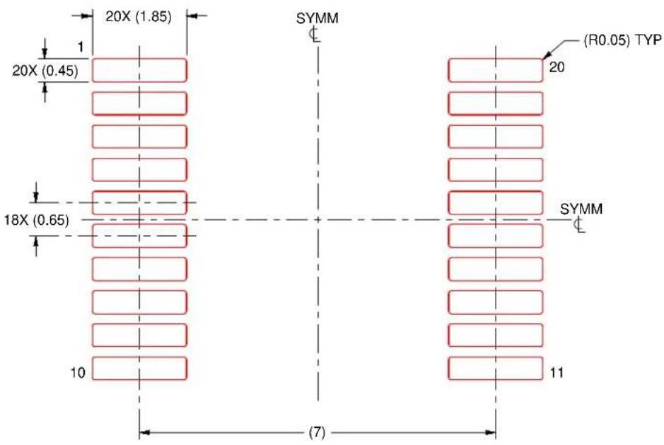
20X (1.85) SYMM (0.45) 1 20X 18X (0.65) 10 (7) (R0.05) TYP 20 SYMM 11LAND PATTERN EXAMPLE
EXPOSED METAL SHOWN
SCALE: 10X
text_image
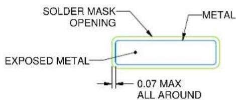
SOLDER MASK OPENING METAL EXPOSED METAL 0.07 MAX ALL AROUNDNON-SOLDER MASK DEFINED (PREFERRED)
text_image
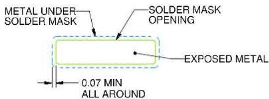
METAL UNDER SOLDER MASK SOLDER MASK OPENING EXPOSED METAL 0.07 MIN ALL AROUNDSOLDER MASK DETAILS
4214851/B 08/2019
NOTES: (continued)
- Publication IPC-7351 may have alternate designs.
- Solder mask tolerances between and around signal pads can vary based on board fabrication site.
SMALL OUTLINE PACKAGE
text_image
20X (1.85) SYMM (0.45) 20X 1 18X (0.65) 10 (7) (R0.05) TYP 20 SYMM 11SOLDER PASTE EXAMPLE
BASED ON 0.125 mm THICK STENCIL
SCALE: 10X
4214851/B 08/2019
NOTES: (continued)
- Laser cutting apertures with trapezoidal walls and rounded corners may offer better paste release. IPC-7525 may have alternate design recommendations.
- Board assembly site may have different recommendations for stencil design.
MECHANICAL DATA
NS (R-PDSO-G\*\*)
PLASTIC SMALL-OUTLINE PACKAGE
14-PINS SHOWN
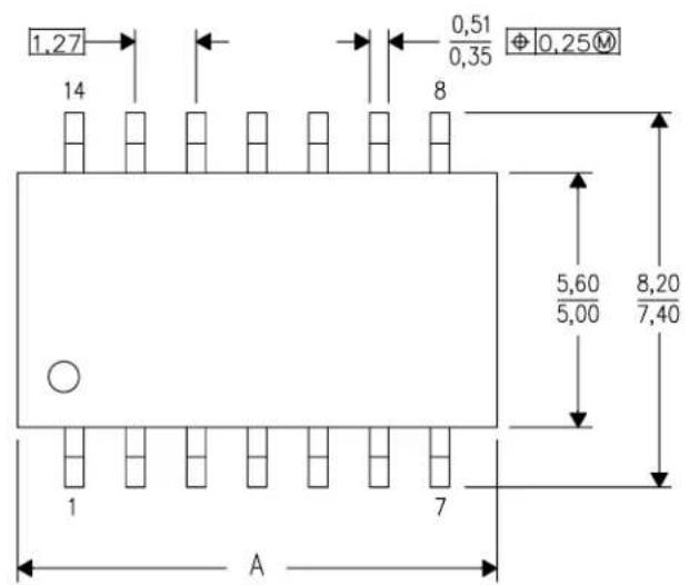
text_image
1,27 14 0,51 0,35 Ø 0,25① 8 5,60 5,00 8,20 7,40 1 7 A
text_image
0,15 NOM Gage Plane 0,25 0°-10° 1,05 0,55
text_image
2,00 MAX 0,15 0,05
text_image
Seating Plane 0.10| DIM\PINS ** | 14 | 16 | 20 | 24 |
| A MAX | 10,50 | 10,50 | 12,90 | 15,30 |
| A MIN | 9,90 | 9,90 | 12,30 | 14,70 |
4040062/C 03/03
NOTES: A. All linear dimensions are in millimeters.
B. This drawing is subject to change without notice.
C. Body dimensions do not include mold flash or protrusion, not to exceed 0,15.
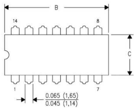
text_image
B 14 8 C 1 0.065 (1,65) 0.045 (1,14)| PINS **DIM | 14 | 16 | 18 | 20 |
| A | 0.300(7,62)BSC | 0.300(7,62)BSC | 0.300(7,62)BSC | 0.300(7,62)BSC |
| B MAX | 0.785(19,94) | .840(21,34) | 0.960(24,38) | 1.060(26,92) |
| B MIN | — | — | — | — |
| C MAX | 0.300(7,62) | 0.300(7,62) | 0.310(7,87) | 0.300(7,62) |
| C MIN | 0.245(6,22) | 0.245(6,22) | 0.220(5,59) | 0.245(6,22) |
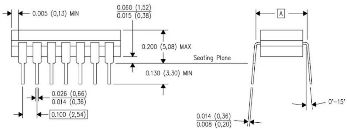
text_image
0.005 (0,13) MIN 0.060 (1,52) 0.015 (0,38) 0.200 (5,08) MAX Seating Plane 0.130 (3,30) MIN 0.026 (0,66) 0.014 (0,36) 0.100 (2,54) 0.014 (0,36) 0.008 (0,20) A 0°-15°4040083/F 03/03
NOTES:
A. All linear dimensions are in inches (millimeters).
B. This drawing is subject to change without notice.
C. This package is hermetically sealed with a ceramic lid using glass frit.
D. Index point is provided on cap for terminal identification only on press ceramic glass frit seal only.
E. Falls within MIL STD 1835 GDIP1-T14, GDIP1-T16, GDIP1-T18 and GDIP1-T20.
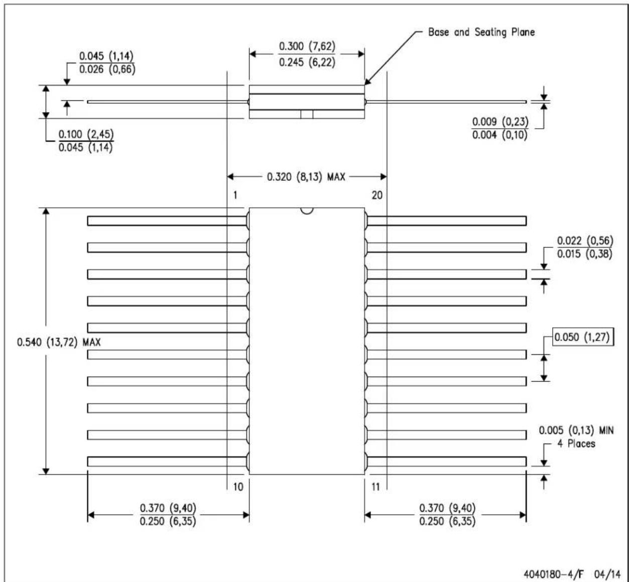
N (R-PDIP-T\*\*)
16 PINS SHOWN
PLASTIC DUAL-IN-LINE PACKAGE

text_image
A 16 9 0.260 (6,60) 0.240 (6,10) 1 8 0.070 (1,78) 0.045 (1,14)C
| DIM\PINS ** | 14 | 16 | 18 | 20 |
| A MAX | 0.775(19,69) | 0.775(19,69) | 0.920(23,37) | 1.060(26,92) |
| A MIN | 0.745(18,92) | 0.745(18,92) | 0.850(21,59) | 0.940(23,88) |
| MS-001VARIATION | AA | BB | AC | AD |
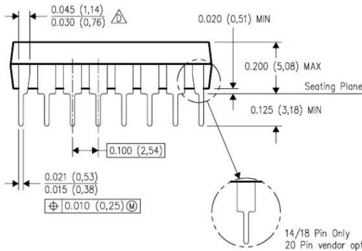
text_image
0.045 (1,14) 0.030 (0,76) D 0.020 (0,51) MIN 0.200 (5,08) MAX Seating Plane 0.125 (3,18) MIN 0.100 (2,54) 0.021 (0,53) 0.015 (0,38) ⊕ 0.010 (0,25) M 14/18 Pin Only 20 Pin vendor opt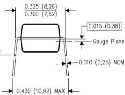
text_image
0.325 (8,26) 0.300 (7,62) 0.015 (0,38) Gauge Plane 0.010 (0,25) NOM 0.430 (10,92) MAX4040049/E 12/2002
NOTES: A. All linear dimensions are in inches (millimeters).
B. This drawing is subject to change without notice.
C Falls within JEDEC MS-001, except 18 and 20 pin minimum body length (Dim A).
The 20 pin end lead shoulder width is a vendor option, either half or full width.
SOIC

4220724/A 05/2016
NOTES:
- All linear dimensions are in millimeters. Dimensions in parenthesis are for reference only. Dimensioning and tolerancing per ASME Y14.5M.
- This drawing is subject to change without notice.
- This dimension does not include mold flash, protrusions, or gate burrs. Mold flash, protrusions, or gate burrs shall not exceed 0.15 mm per side.
- This dimension does not include interlead flash. Interlead flash shall not exceed 0.43 mm per side.
- Reference JEDEC registration MS-013.
SOIC
text_image
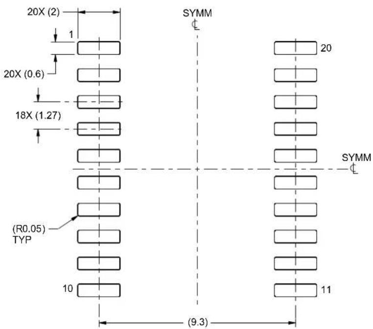
20X (2) 1 20X (0.6) 18X (1.27) (R0.05) TYP 10 SYMM 20 SYMM 11 (9.3)LAND PATTERN EXAMPLE SCALE:6X

text_image
SOLDER MASK OPENING METAL 0.07 MAX ALL AROUNDNON SOLDER MASK DEFINED
text_image
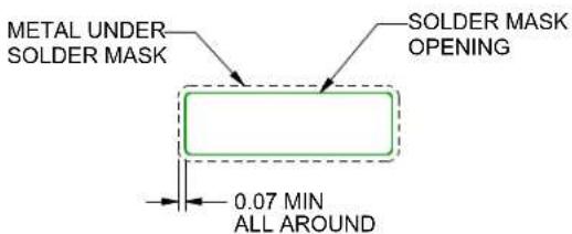
METAL UNDER SOLDER MASK SOLDER MASK OPENING 0.07 MIN ALL AROUNDSOLDER MASK
DEFINED
SOLDER MASK DETAILS
4220724/A 05/2016
NOTES: (continued)
- Publication IPC-7351 may have alternate designs.
- Solder mask tolerances between and around signal pads can vary based on board fabrication site.
SOIC
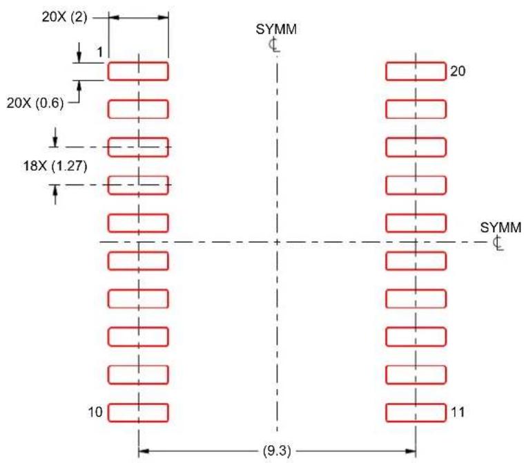
text_image
20X (2) 1 20X (0.6) 18X (1.27) SYMM 20 SYMM 10 (9.3) 11SOLDER PASTE EXAMPLE
BASED ON 0.125 mm THICK STENCIL
SCALE:6X
4220724/A 05/2016
NOTES: (continued)
- Laser cutting apertures with trapezoidal walls and rounded corners may offer better paste release. IPC-7525 may have alternate design recommendations.
- Board assembly site may have different recommendations for stencil design.
IMPORTANT NOTICE AND DISCLAIMER
TI PROVIDES TECHNICAL AND RELIABILITY DATA (INCLUDING DATA SHEETS), DESIGN RESOURCES (INCLUDING REFERENCE DESIGNS), APPLICATION OR OTHER DESIGN ADVICE, WEB TOOLS, SAFETY INFORMATION, AND OTHER RESOURCES "AS IS" AND WITH ALL FAULTS, AND DISCLAIMS ALL WARRANTIES, EXPRESS AND IMPLIED, INCLUDING WITHOUT LIMITATION ANY IMPLIED WARRANTIES OF MERCHANTABILITY, FITNESS FOR A PARTICULAR PURPOSE OR NON-INFRINGEMENT OF THIRD PARTY INTELLECTUAL PROPERTY RIGHTS.
These resources are intended for skilled developers designing with TI products. You are solely responsible for (1) selecting the appropriate TI products for your application, (2) designing, validating and testing your application, and (3) ensuring your application meets applicable standards, and any other safety, security, regulatory or other requirements.
These resources are subject to change without notice. TI grants you permission to use these resources only for development of an application that uses the TI products described in the resource. Other reproduction and display of these resources is prohibited. No license is granted to any other TI intellectual property right or to any third party intellectual property right. TI disclaims responsibility for, and you will fully indemnify TI and its representatives against, any claims, damages, costs, losses, and liabilities arising out of your use of these resources.
TI's products are provided subject to TI's Terms of Sale or other applicable terms available either on ti.com or provided in conjunction with such TI products. TI's provision of these resources does not expand or otherwise alter TI's applicable warranties or warranty disclaimers for TI products.
TI objects to and rejects any additional or different terms you may have proposed.
Mailing Address: Texas Instruments, Post Office Box 655303, Dallas, Texas 75265
Copyright © 2022, Texas Instruments Incorporated