FR II - Videokamera KYOCERA - Kostenlose Bedienungsanleitung
Finden Sie kostenlos die Bedienungsanleitung des Geräts FR II KYOCERA als PDF.

| Produkttyp | Videokamera |
| Marke | Kyocera |
| Modell | FR II |
| Abmessungen (B x H x T) | ca. 120 x 100 x 200 mm |
| Gewicht | ca. 800 g (ohne Akku und Kassette) |
| Stromversorgung | Netzteil (DC 7,2 V) oder Akku (Ni-Cd, 7,2 V) |
| Leistungsaufnahme | ca. 5 W |
| Bildsensor | 1/3-Zoll-CCD, ca. 270.000 Pixel |
| Objektiv | Zoom 6:1, Brennweite 5,4–32,4 mm |
| Blende | F1.6–2.4 |
| Videokomprimierung | Analog (8-mm-Video) |
| Speichermedium | 8-mm-Videokassette |
| Bildschirm | 0,7-Zoll-EVF (elektronischer Sucher) |
| Audio | Mono-Ton, eingebautes Mikrofon |
| Anschlüsse | AV-Ausgang (Cinch), Mikrofoneingang (3,5 mm) |
| Hauptfunktionen | Autofokus, Weißabgleich, Aufnahme, Wiedergabe |
| Reinigung und Pflege | Gehäuse mit weichem, trockenem Tuch reinigen; Objektiv mit Linsenreinigungsset |
| Sicherheitshinweise | Nicht in Wasser tauchen; von heißen Oberflächen fernhalten; nur Originalzubehör verwenden |
| Ersatzteile und Reparierbarkeit | Ersatzakkus und -netzteile verfügbar; Reparatur durch Fachbetrieb |
| Allgemeine Informationen | Urheberrecht © 2023 Kyocera; Bedienungsanleitung als PDF herunterladbar |
Häufig gestellte Fragen - FR II KYOCERA
Benutzerfragen zu FR II KYOCERA
0 Frage zu diesem Gerät. Beantworten Sie die, die Sie kennen, oder stellen Sie Ihre eigene.
Eine neue Frage zu diesem Gerät stellen
Laden Sie die Anleitung für Ihr Videokamera kostenlos im PDF-Format! Finden Sie Ihr Handbuch FR II - KYOCERA und nehmen Sie Ihr elektronisches Gerät wieder in die Hand. Auf dieser Seite sind alle Dokumente veröffentlicht, die für die Verwendung Ihres Geräts notwendig sind. FR II von der Marke KYOCERA.
BEDIENUNGSANLEITUNG FR II KYOCERA
YASHICA
FRⅠ/FRⅡ
REPAIR MANUAL
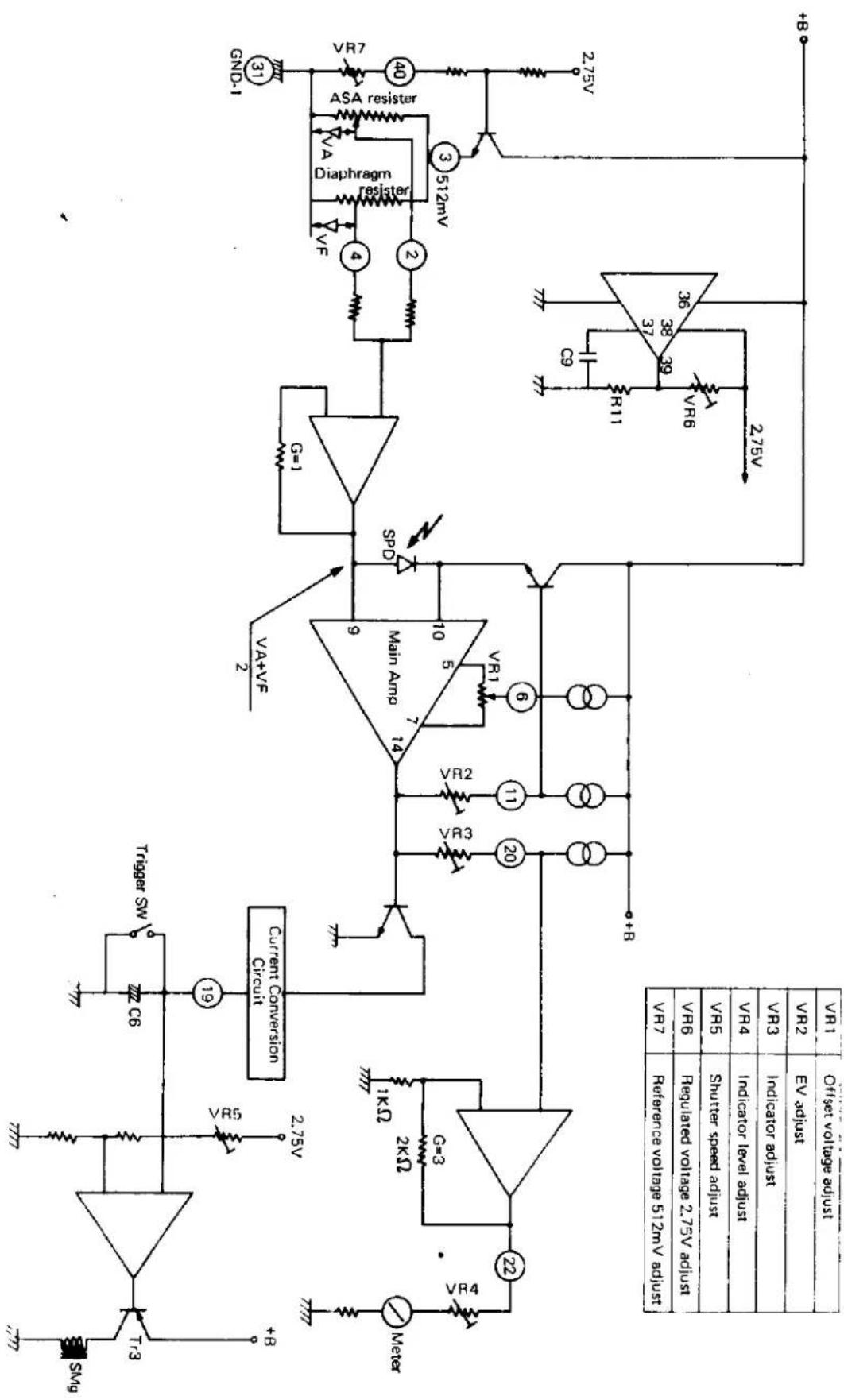
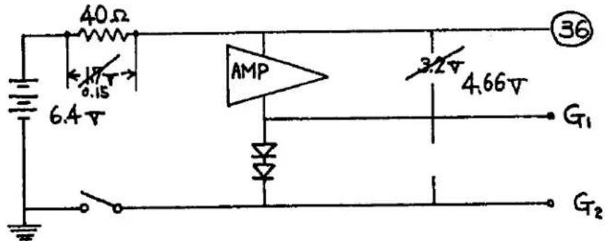
Voltage Measurement
Conditions: ASA 100, without lens (equivalent to F 1.2), natural light, Exposure Check switch ON in AUTO mode.
NOTE: In certain cases, the output voltage measured will vary. The following voltage levels depend somewhat on external conditions.
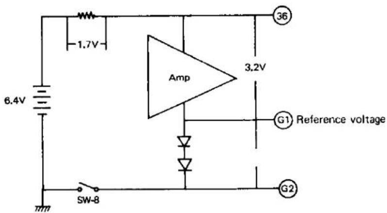
line
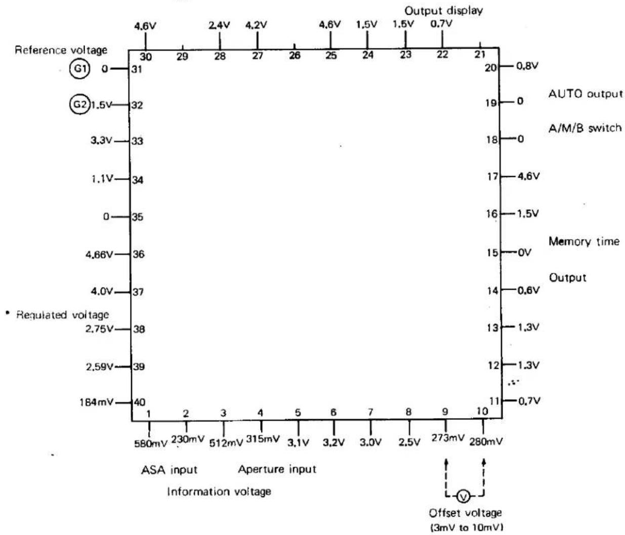
| Input | Voltage (mV) | |---|---| | Reference voltage | 4.6 | | G1 | 30 | | G2 | 32 | | 3.3V | 33 | | 1.1V | 34 | | 0 | 35 | | 4.66V | 36 | | 4.0V | 37 | | 2.75V | 38 | | 2.59V | 39 | | 184mV | 40 | The chart displays the output display and its corresponding input voltage values for each input type. The input voltage ranges from 0.7V to 580mV, while the output voltage ranges from 0.8V to 1.5V. The diagram includes an inset schematic illustrating the offset voltage (3mV to 10mV) with a voltage symbol.Defects in reference voltage
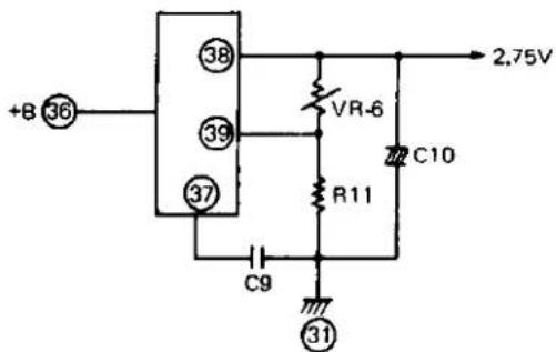
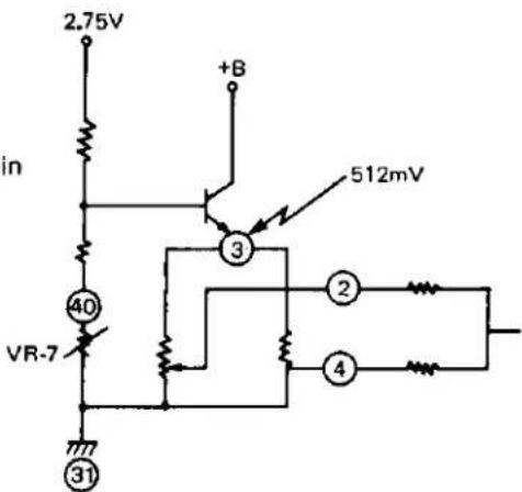
1. Regulated 2.75 V not obtained.
a. Defective VR-6.
b. Defective R 11.
c. Defective C 10.
d. Opened FPC circuit.
Circuit 31
VR-6 to ③9 or ③8
etc.
e. Defective IC.
2. Information voltage (512 mV) not obtained.
a. Defective VR-7.
b. Defective aperture resistor (opened).
c. Defective insulation in aperture resistor.
d. Defective ASA resistor.
Defective soldering at connector pin
②, ③ or ④.
e. Opened FPC circuit.
R_ASA to ②, ③ or ④
VR-7 to ④0
f. Defective IC.
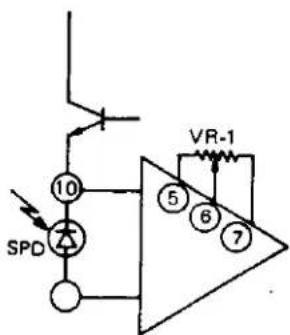
3. No offset voltage
a. Defective VR-1 (solder-bridged circuit pattern).
b. Defective SPD (solder-bridged circuit pattern).
c. Opened FPC circuit.
SPD to IC pin ⑨ or ⑩
VR-1 to IC pin ⑤, ⑥ or ⑦
d. Defective IC.
\* Possible symptoms of the above troubles:
- Shutter not triggered.
- Aperture open at AUTO mode, slow aperture response, or aperture motion not smooth.
- Shutter opens before triggering.
- Incorrect operation due to external conditions.
Shutter not open
No shutter opening
Conditions: Check that 2.75 V, 512 mV output and offset voltage are normal and wiring is correct.
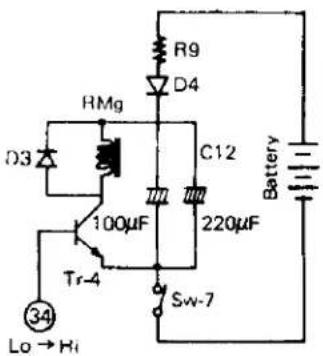
Shutter not open at either of A, B, M or F mode, but approximately 30 mA current continues to flow after Release set at ON (latched).
(Signal appears at Tr 4 input).
- Defective Tr 4,
- Defective C 12.
- Defective R 9.
- Defective D 4.
- Defective D 3.
- Defective R Mg.
- Defective contact in Power SW.
- Defective contact between R_ASA WHITE lead and connector.
- Excess engagement between RL 1 and 2.
- Opened FPC wiring.
- Defective soldering.
No electric current with Release at ON.
- GND screw floated from chassis.
- Defective conduction in Timing SW.
- Defective conduction in Release SW.
- Opened wiring (RED, WHITE, GRAY, BLACK or YELLOW GREEN leads etc.)
Approximately 20 mA current continues to flow with Exposure Check at OFF and Release at OFF.
- Defective C 12 (short-circuited).
No shutter opening in A or B mode, though the shutter functions normally in M or F mode. (Approximately 30 mA flows momentarily with Release at ON, but there is no current with Release at OFF (not latched).
-
No offset voltage (LED remains lit).
a. Defective VR-1.
b. Defective SPD.
c. Opened FPC wiring
VR-1 to IC pin
⑤, ⑥ or ⑦
SPD to IC pin
⑨ or ⑩ -
Memory time not obtained.
a. Defective R 4.
b. Defective C 3.
c. Defective soldering to B 4 or C 3.
d. Opened FPC wiring.
Shutter not open in dark (in AUTO mode).
-
LED not lit.
a. Defective R 10.
b. Defective LED.
c. Opened FPC circuit. -
Oscillating circuit.
a. Defective ranking by R 10.
b. Offset voltage not obtained.
• The oscillation will stop and the shutter open normally when a resistor 2R 10 is connected parallel with LED.
Defective IC (replacement of Amp. required).
- No shutter opening with Exposure Check ON and Release ON.
- No shutter opening in B mode with Exposure Check ON and Release ON.
- No shutter opening at 6.4 V and 150 ohm.
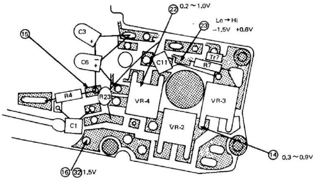
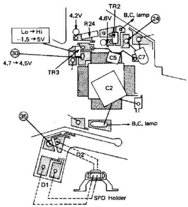
| Symbol | Component | Function | Defect |
| VR 2 | 4.7 kΩ semi-fixed VR. | Exposure control. | Slow shutter speeds at AUTO (poor EV output). Opened or abnormal shutter operation at AUTO. |
| VR 3 | 150 kΩ semi-fixed VR. | Meter sensitivity control. | Meter is not adjustable (no pointer motion). |
| VR 4 | 1 kΩ semi-fixed VR. | Meter level adjustment. | Same as above. (pointer range) |
| R 23 | 6.8 MΩ (142) fixed resistor.9.1 MΩ (143) fixed resistor. | Shutter-speed control in dark. | Shutter remains open in the dark, or insufficient EV information at low light intensity. |
| R 4 | 160 kΩ fixed resistor.0.22 μF dipped tantalum capacitor. | Presetting of memory time (23 ms.) | Shutter not open, or EV information not stable (in AUTO with aperture fully open). |
| C 6 | 0.47 μF dipped tantalum capacitor. | Charging time of this capacitor is used to control shutter speeds. | Shutter speeds skipped, shutter remains open, or incorrect shutter speeds. |
| C 11 | 4700 pF Ceramic capacitor. | Protects the circuit from reverse electromotive force of SMg. | Abnormal shutter operation. |
| C 1 | 100 pF Ceramic capacitor. | Protects the circuit from oscillation. | Unstable EV information with aperture fully opened in AUTO mode, or no shutter opening. |
| Tr-1 | L 7 mini-transistor. | A latching transistor (functions as a main switch at shutter opening). | No latching, shutter opens before triggering, or remains open in B mode. |
| R 7 | 10 kΩ fixed resistor. | Supplies the base current to Tr-1. | Same as above. |
| Symbol | Component | Function | Defect |
| I C | C 1106 integrated circuit. | Controls entire electric circuit. | |
| C 2 | 0.022 μF film capacitor. | A memory capacitor. | Insufficient or unstable EV information (particularly at low light intensity). |
| C 7 | 0.22 μF dipped tantalum capacitor. | Protects the circuit from abnormal operation. | Shutter opened before triggering (at Exposure Check ON to OFF), or no latching. |
| C 5 | 4700 pF ceramic capacitor. | Protects the circuit from oscillation. | Unstable EV information, or abnormal operation. |
| Tr-2 | L 7 mini-transistor. | Battery Check lamp driver. | BC lamp not lit. |
| R 24 | 5.1 kΩ fixed resistor. | Supplies signal to the base base of Tr-2. | BC lamp not lit. |
| Tr-3 | M 6 mini-mold transistor. | Drives SMg. | Skipped shutter speeds or shutter remains open. |
| D 1 | SPD | Light-input measurement. | Shutter not opened (no offset voltage) (Skipped shutter speeds at AUTO, shutter remains open or insufficient EV information). |
| D 2 | SG2-04B LED | Preliminary SPD driver. | Shutter not open, insufficient EV information or no shuttering at low subject brightness. |
| VR-1 | 22 kΩ semi-fixed VR. | Offset voltage adjustment.(balancing control). | Shutter not open, insufficient EV information or abnormal operation. |
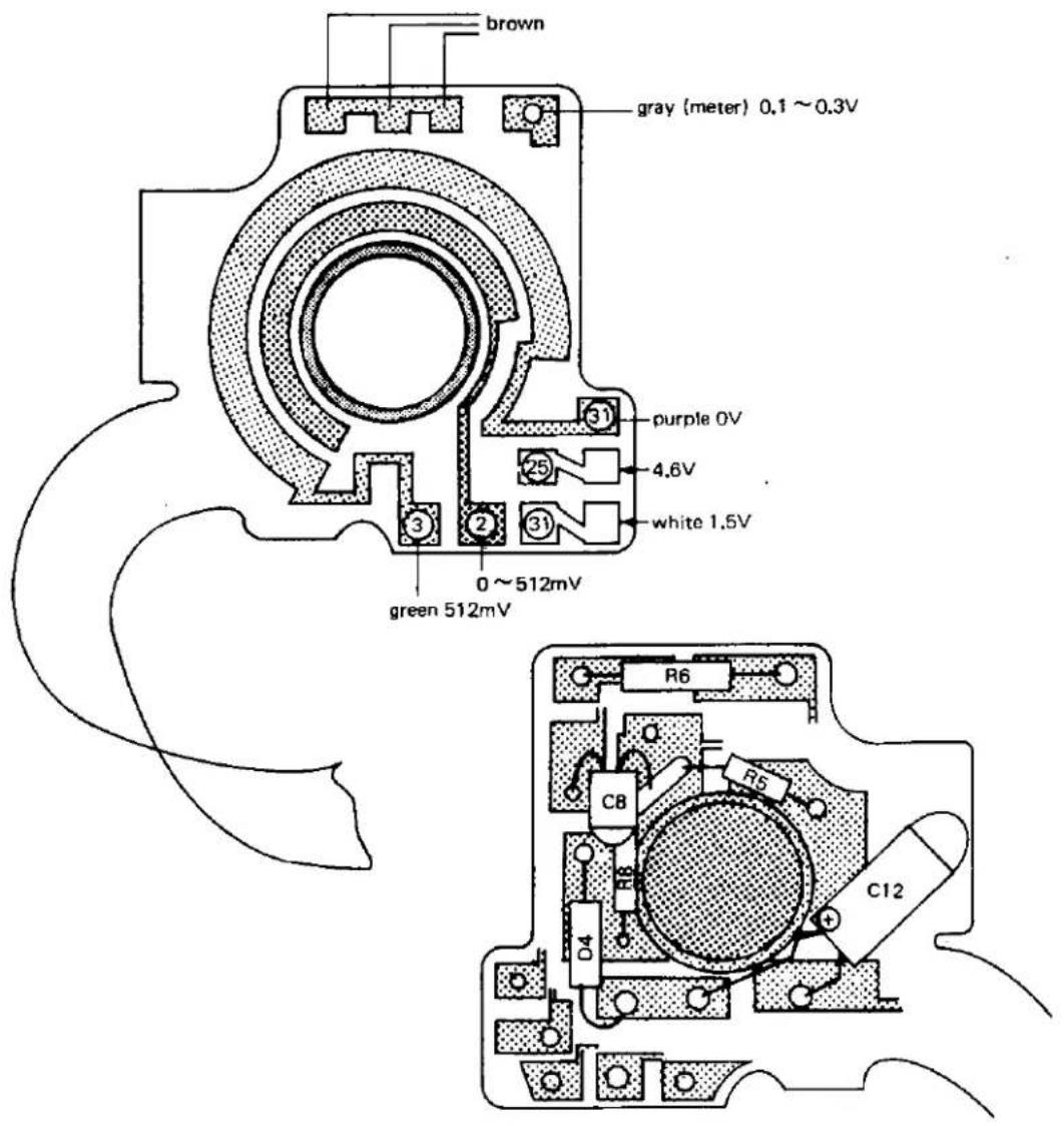
| R 10 | Selective resistor. | Resistance value selected according to sensitivity of SPD.Rank A 300 ΩRank B 620 ΩRank C 1.2 kΩRank D 2.4 kΩ | No shutter opening at low subject brightness, or unstable EV information. |
| VR 5 | 47 kΩ semi-fixed VR. | Level adjustment (seconds).(seconds). | Skipped shutter speeds (A, B, M, ) or incorrect second-settings (slow or fast). |
| R 1 | 120 kΩ Fixed resistor. | Thermal compensation resistor (a metallic film resistor). | Incorrect shutter speeds in AUTO mode, or low meter indication. |
| VR 6 | 6.8 kΩ Semi-fixed VR. | Voltage setting (regulated 2.75 V). | Incorrect reference voltage (not 2.75 V), or abnormal circuit operation. |
| R11 | 20 kΩ fixed resistor. | A breeder resistor in 2.75 V regulator. | Incorrect reference voltage. |
| C 10 | 0.68 μF dipped tantalum capacitor. | Voltage regulation capacitor. | Unstable voltage output (2.75 V) or abnormal circuit operation. |
| C 9 | 22000 pF ceramic capacitor. | Voltage regulation capacitor. | Same as above. |
| C 4 | 0.33 μF dipped tantalum capacitor. | Protects the circuit from abnormal operation (high cut filter across G 1 and G 2). | Abnormal operation (shutter opens before triggering). |
| VR 7 | 3.3 kΩ semi-fixed VR. | Information voltage adjustment (512 mV). | Incorrect 512 mV output, no. offset voltage, or insufficient EV information (Skipped shutter speeds). |
| Symbol | Component | Function | Defect |
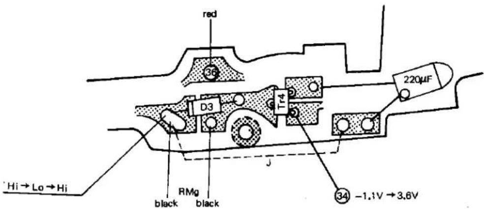
| D 3 | IS 953 Si diode | Protects the circuit from reverse electromotive force of RMg. | No shutter opening. |
| Tr-4 | B 4 mini-mold transistor. | Drives RMg. | No shutter opening, or shutter opens before triggering. |
| C 12 | 220 μF dipped tantalum capacitor. | Energy storage for proper shutter response. | No shutter opening, or incorrect shutter operation. |
| Connector terminal | Normal voltage | AT defective contact |
| 3 | 512 mV | Shutter remains open in AUTO mode (0 V). |
| 2 | 0 to 512 mV | Shutter speeds not linked to ASA setting.Slow shutter speeds in AUTO mode. |
| 31 | 1.5 V | 2 to 4 V, no shutter opening or B.C. lamp not lit. |
| 25 | 4.6 V | If 0 V, B.C. lamp not lit. |
| 31 | 0 V | 0.8 to 4 V, 512 mV not obtained, shutter remains open in AUTO mode. |
| Symbol | Component | Function | Defect |
| R 6 | 1.1 kΩ fixed resistor. | Thermal compensation resistor for meter indicator (provided with reverse thermal characteristics to internal resistance of meter). | No meter indication, meter is not adjustable or weak indicator |
| C 8 | 1 μF dipped tantalum capacitor. | Regulates power voltage. | Abnormal circuit operation. |
| R 5 | 160 kΩ fixed resistor. | ||
| R 8 | 150 Ω fixed resistor. | Charges Mg2 actuator capacitor C 12. | No shutter opening. |
| D 4 | 1K-60 Ge diode | Stops reverse current. | No shutter opening. |
| C 12 | 100 μF dipped tantalum capacitor. | Stores electric power to actuate Mg2. | No shutter opening, or incorrect shutter speeds. |
MDC base plate
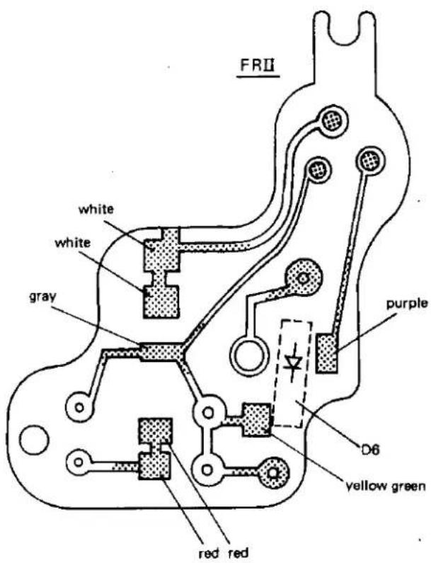
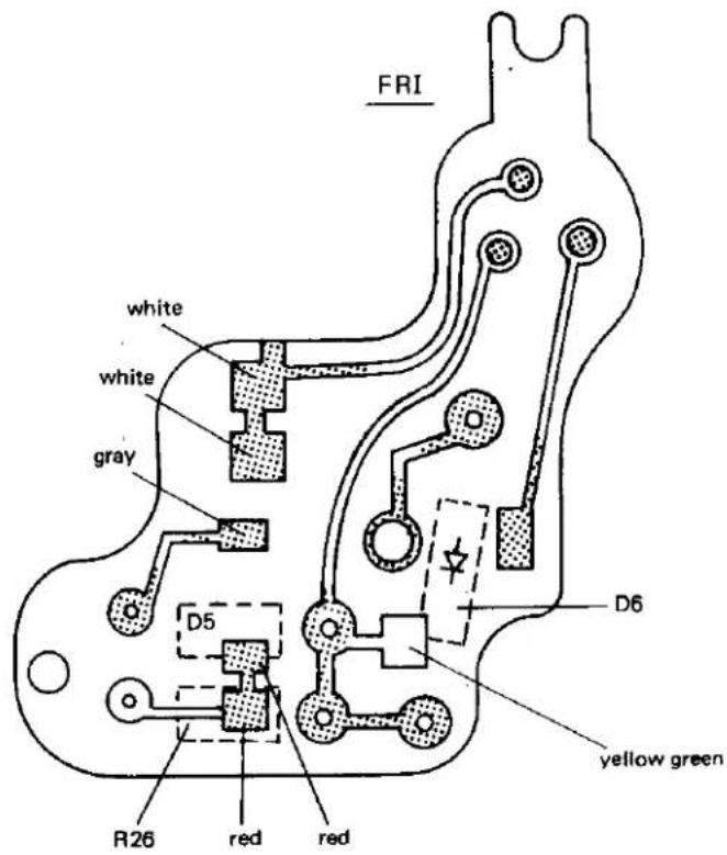
D 6 : Zener diode (B 7) —— Protects the circuit from damage when S.P. is set by mistake to R.S.
Reversed diode polarity ---- Shutter opens before triggering.
142: Normal with Exposure Check at ON, but shutter opens when film lever is advanced with Exposure Check at OFF.
143: Shutter opens before triggering with Exposure Check at ON/OFF.
Diode missed ---- Shutter functions normally, but no protective function.
D 5: Si diode (IS 953)
Data-back signalling with Exposure Check SW at ON.
R26 : Fixed resistor (10 kΩ)
Defects: ○ No shutter opening.
o Large current flows with Exposure Check SW at ON or Release at ON.
○ Data-back signal is not obtained with Exposure Check SW at ON.
No shutter opening
- Opened FPC pattern between 34P and Tr4. (Possibly damaged with tweezers when assembling wire leads).
- Detective soldering of BLUE wire on module and R4.
- Reversed D3 polarity.
Short-circuitted C3 (+) and C6 (-): Memory time not obtained.
b. Jumper wire located below LED N resistor is short-circuitted to RF.
- The circuit cannot enter next operation sequence because the short-circuitting drives LED N circuit always ON.
- Opened Vcc jumper wiring (J4).
- Defective contact to C12 (shutter operation is not smooth), defective contact to C3 (+) (no shutter opening), C12 missed or wired to reverse polarity (shutter operation is not smooth).
- Excessive resistance of R9 (normally 150Ω, but a 160kΩ resistor may have been wired).
* Repeated shuttering impossible (too long charging time required).
- J4 disconnected.
- Opened Tr4 B4E,
- RL 1 and 2 require readjustment.
- Opened RED power wiring (defective soldering), or short-circuitted (mistake in assembly).
- Opened wiring to SPD (defective soldering).
- Jumper wire to MDC module missed (143) or short-circuitted.
- Short-circuitted or RED wire in module wired in error.
- MDC module GRAY wire short-circuitted to top cover or wired in error.
- Defective contact in timing SW.
- RMg wire (BLACK) short-circuitted to case or opened.
- Opened wiring to or defective soldering on WHITE ASA connector pins.
- Defective contact in Power SW.
- Incorrect pin-position in PURPLE wire connector on ASA board.
- Wire lead of D3 penetrated FPC and short-circuitted to SP shaft.
- Opened wiring (BLACK) to Release SW.
No shutter opening at low subject brightness
- Bridged wirings to LED, (LED N will not light).
- Defective soldering to R10.
Shutter opens before triggering
- Short-circuitted Release Socket.
- PURPLE wire to MDC module grounded to body or wired in error.
- Incorrect operation of SMg armature.
- SMg wire (BLACK) wired to G1 in error or short-circuitted to ASA resistor board.
- M link plate short-circuitted to Manual resistor.
- Reversed zener diode polarity on MDC module.
- Trigger SW short-circuited to 1st curtain release lever.
- Short-circuitted C3 terminals.
- GRAY wire short-circuitted to top cover.
512mV output not obtained
- Defective contact in ASA resistor board of GREEN or PURPLE wire to connector.
- Opened FPC circuit.
- Opened FPC pattern between IC pin ③ and ASA resistor.
- VR 7 is not 3.3kΩ.
- Defective soldering to AMP repeating pins (See 1.)
2.75V output not obtained
- IC pin 16 opened (defective soldering to PINK wire).
- Defective contact in Slide SW.
- Unstable VR6 setting.
- GREEN wire wired in error.
No offset voltage
- Wiring error to Trigger SW (YELLOW wire).
- Incorrect brush setting or opened brush contact on ASA resistor.
- Erroneous wiring (PURPLE or GREEN) to Aperture Resistor, or reversed ORANGE and YELLOW wirings.
- Opened jumper (BROWN).
- Defective soldering to SPD.
- IC pins ② and ③ bridged by solder.
Unstable high-speed limiter
- Insufficient timing adjustment for offset voltage.
- Timing SW shatters.
- Defective contact to R4 (excessively long memory time).
No meter indication
- Wiring error to meter (ORANGE), Aperture resistor (YELLOW), or wiring error of GRAY wire (or shorted to top cover).
- Excessive value of R6 (should normally be 1kΩ). In this case, the shutter speeds are normal but are not indicated on the meter.
- ASA resistor rubs meter pointer.
- R6 is missed.
Incorrect shutter speeds
- Opened SMg (shutter not opened), or wiring short-circuitted to top cover.
- Defective contact to the base of Tr3.
- Opened J5 connection. Incorrect speeds at 1/8 to 1, but speeds 1/100 to 1/15 are normal.
- Wiring erroe (YELLOW) to Trigger SW.
AUTO, N make and B are normal: Error in YELLOW wiring.
No shutter opening at 1/60 to 1/1000. - SAS G1 pin opened. (Occasional shutter errors.)
- Smeared shutter resistor board (shutter will not open).
Incorrect B operation
- Error in YELLOW wiring to Trigger SW.
- Defective contact to Tr1 pin (slow shutter speeds not obtainable).
- Defective soldering to PINK wiring.
- Defective contact to C6 terminal (incorrect B operation and shutter remains open at N).
- Incorrect positioning or defective contact of C3 or C6 pin. Signal waveform appears across G1, IC pin ② and C7 ⊕ at B operation.
- Manual resistor repeating pin opened (defective soldering). Contacts GND (a 1/2 scale too soon) (when turning shutter speed dial to B position).
Shutter remains open in B mode
- Incorrect positioning of Manual Contact, or missed repeater pin.
- Defective soldering to AMP repeater pin.
- Defective contact between 24P connector to Manual Resistor connector pin.
- 06 pin (+) not soldered to Shutter Resistor board.
- Unstable VR2 setting.
- Timing SW chatters.
Shutter remains open in Manual Mode
- Defective contact to Manual Resistor.
Shutter remains open in AUTO mode
- 1C pins 38 and 39 bridged by solder. Shutter remains open in A, no shutter opening in M but normal in B mode. Meter functions normally at Exposure Check with the Film Lever still, but stops and 50mA current continues when the Film Lever is advanced.
- Defective contact in Shutter contacts.
- Smeared Manual Board. LED does not light, but shutter occasionally fails to close.
- Defective soldering to R4.
- Defective soldering to ASA connector pin.
- Excessive VR2 (normally 47kΩ). For example, if a 150kΩ VR was fitted.
- Defective soldering to Manual Resistor, Timing SW chatters.
Shutter remains open at

- Defective soldering to repeater pin.
- Defective soldering to R23.
- Opened wiring to VR2, 47kΩ.
- Defective soldering to Manual Resistor or C3 (the shutter is normal in A mode).
- resistor is missed.
Checker Lamp does not light
- Lamp filament burnt out.
- Smeared or damaged Checker board, Incorrect contact position (or short-circuitting to top cover).
- C10 is missed (Checker lamp faint).
LED does not light
- Error in jumper wiring.
- Opened R10( N ).
- Error in wiring to J3.
Shutter is incidently opened at Exposure Check ON/OFF
- Defective soldering to C7, or capacitor C7 is missed.
- Defective cotact to ASA resistor lead (PURPLE).
Data-back fails to operate
- Defective soldering to MDC jumper.
- Opened AMP circuit pattern.
- Defective soldering to GREEN wire.
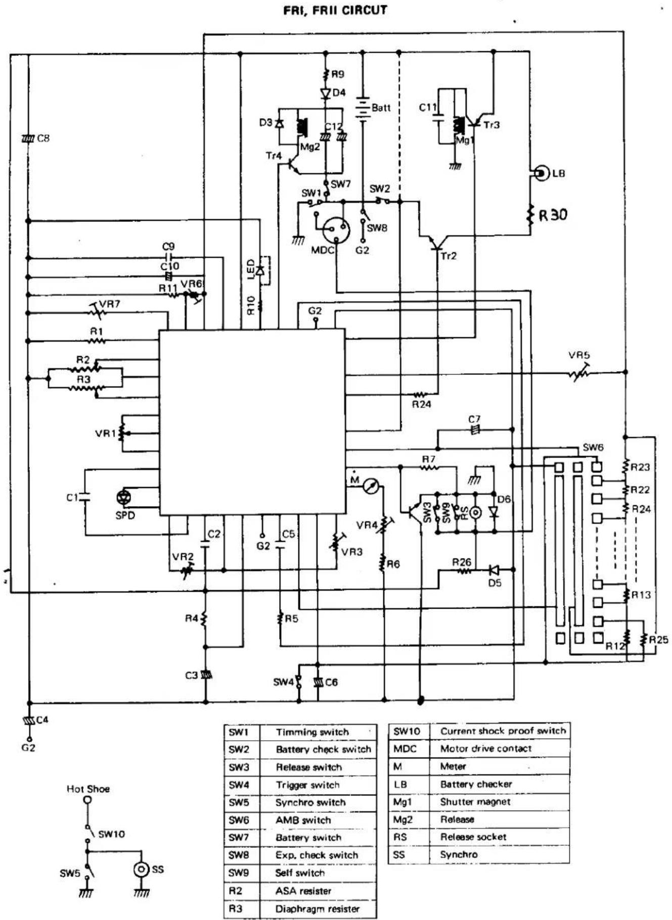
| SW1 | Timmig switch |
| SW2 | Battery check switch |
| SW3 | Release switch |
| SW4 | Trigger switch |
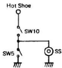
| SW5 | Synchro switch |
| SW6 | AMB switch |
| SW7 | Battery switch |
| SW8 | Exp, check switch |
| SW9 | Self switch |
| R2 | ASA resistor |
| R3 | Diaphragm resistor |
| SW10 | Current shock proof switch |
| MDC | Motor drive contact |
| M | Meter |
| LB | Battery checker |
| Mg1 | Shutter magnet |
| Mg2 | Release |
| RS | Release socket |
| SS | Synchro |
| VR1 | Offset voltage adjust |
| VR2 | EV adjust |
| VR3 | Indicator adjust |
| VR4 | Indicator level adjust |
| VR5 | Shutter speed adjust |
| VR6 | Regulated voltage 2.75V adjust |
| VR7 | Reference voltage 5.2MV adjust |
Shutter resistor
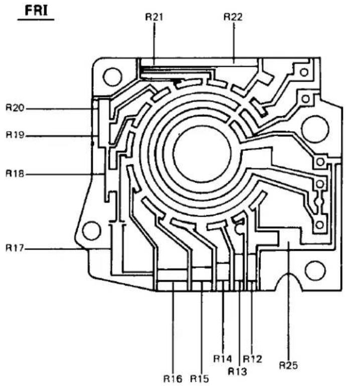
| R-12 | 2KΩ print resistor |
| R-13 | 2" |
| R-14 | 4" |
| R-15 | 8" |
| R-16 | 16.6" |
| R-17 | 33" |
| R-18 | 66.7" |
| R-19 | 125" |
| R-20 | 250" |
| R-21 | 500" |
| R-22 | 1MΩ" |
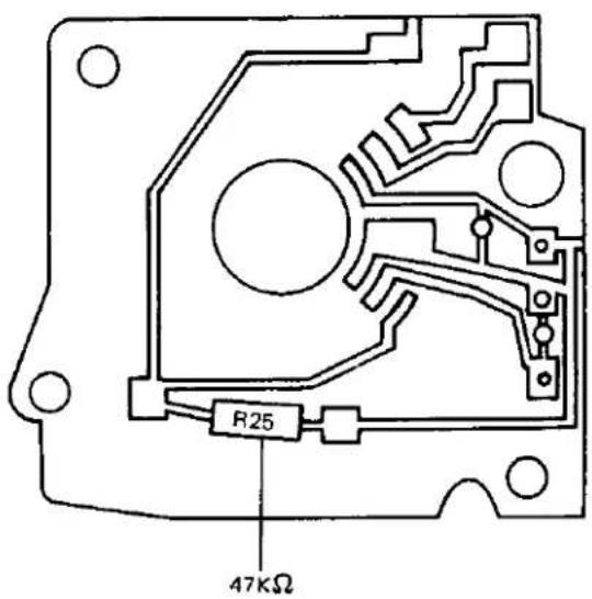
| R-25 | 47KΩ" |
FRII
YASHICA INC.
411 SETTE DRIVE, PARAMUS, NEW JERSEY 07652
TELEPHONE: (201) 262-7300 - (212) 468.5566
CHANGES AND ADDITIONS FOR FR-I & FR-II REPAIR MANUAL
Page 1 -- Add the following:
When checking the camera voltage on the circuit, an external power supply must be used (voltage setting must be 6.4v). HOWEVER, before checking the voltage, put a 40Ω resistor on the high voltage line, between the power supply and the camera body.
Page 2 -- In the section beginning with "Possible symptoms of the above troubles."
2 -- change the word "aperture" to "shutter" in all three places.
Page 4 -- in the chart --
Symbol VR2 - should read "47KΩ."
Symbol R4 - add "C3" to correspond with the second component listing.
Page 5 --
natural_image
Simple line drawing of a mechanical or electrical component with no visible text, numbers, or symbols.YASHICA INC.
411 SETTE DRIVE, PARAMUS, NEW JERSEY 07652
TELEPHONE: (201) 262.7300 - (212) 466.5566
Page 6 -- in the chart --
Symbol R10 should read, under COMPONENT, "LED resistor," which has the same meaning as "selective resistor."
Page 10 -- in the first box, labeled D6:
S.P. means "syncro plug" R.S. means "release socket"
Page 11 -- #1 should read:
"Opened FPC pattern between 34P and Tr4 base"
"22 should read:
"Wire lead of D3 penetrated FPC and short-circuited to spring of rewind shaft."
Page 12 -- under heading of "Incorrect shutter speeds":
4 -- the word "make" should be changed to "mark"
5 -- delete the entire sentence
Page 16 -- Drawing of the shutter resistor for the FR-I should be as such:
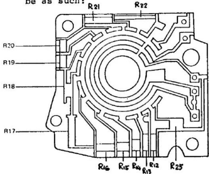
| R-12 | 2KΩ print resistor |
| R-13 | 2" |
| R-14 | 4" |
| R-15 | 8" |
| R-16 | 16.6" |
| R-17 | 33" |
| R-18 | 66.7" |
| R-19 | 125" |
| R-20 | 250" |
| R-21 | 500" |
| R-22 | 1MΩ" |
| R-25 | 47KΩ" |
YASHICA INC.
411 SETTE DRIVE, PARAMUS, NEW JERSEY 07652
TELEPHONE: (201) 262-7300 - (212) 468.5566
Page 8 -- In the diagram, it must read R9 - not R8...as follows below:
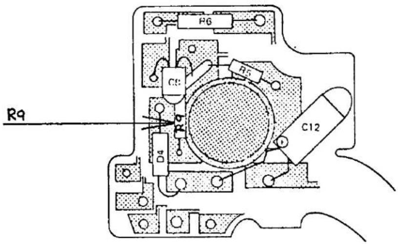
Page 9 -- In this chart, R8 is incorrect; it should read R9.
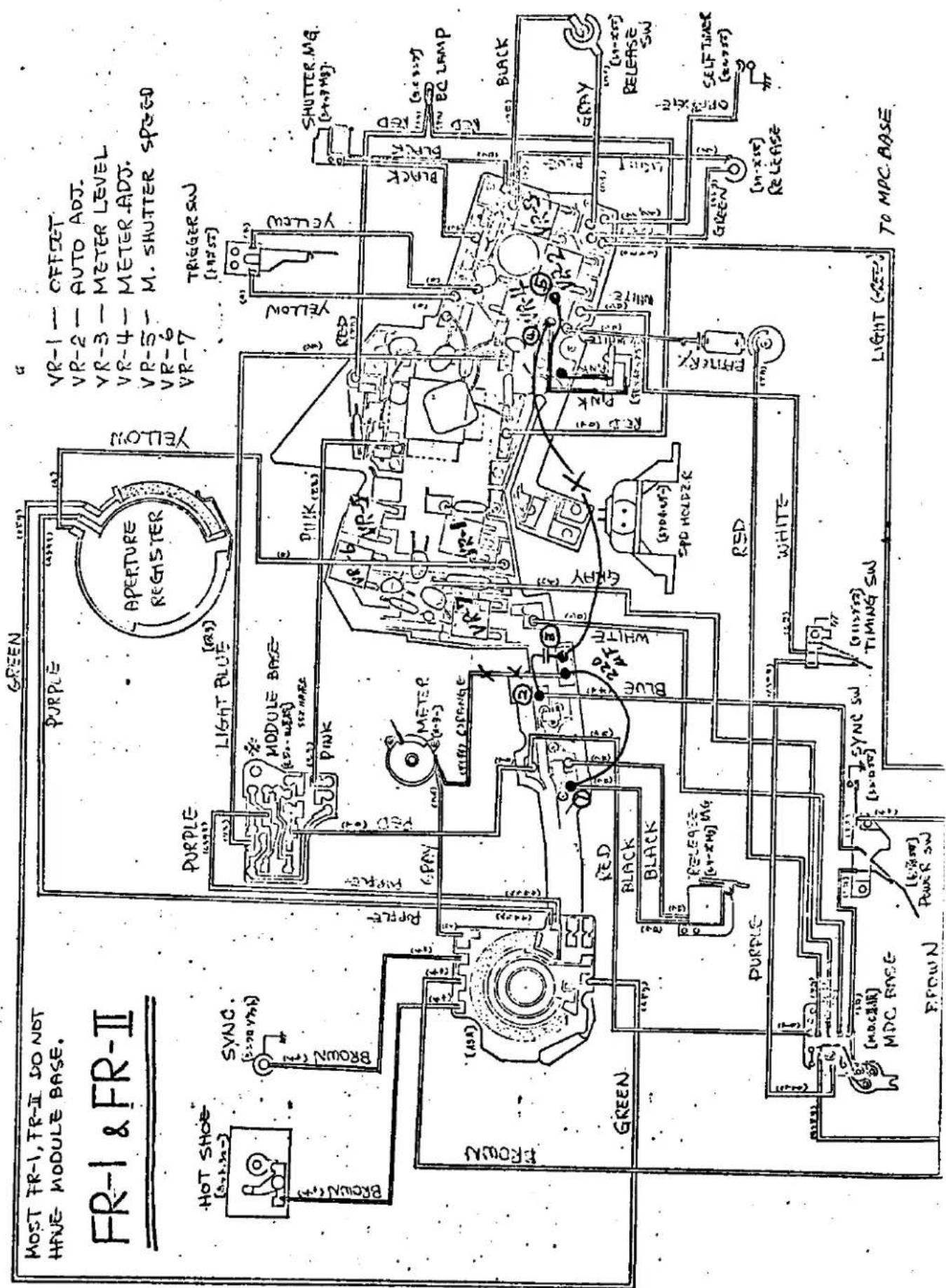
PLEASE NOTE THE ATTACHED AMENDED WIRING DIAGRAM
FOR THE YASHICA FR-I & FR-II. THE NEW MODELS
OF THESE CAMERAS HAVE A CAPACITOR (220μF),
AND THE PROPER WIRING INSTRUCTIONS ARE AS
FOLLOWS:
(Please see diagram to determine wire colors)
1) PINK wire should not be connected to #4, but to #5. This is true of all FR-I & II, old or new.
2) On models with the capacitor, the wire which is now connected from #3 to #4 must be disconnected, and a connection must be made from #1 to #3.
3) The capacitor must now be connected between #2 and #3.
4) The orange wire from the meter was previously connected to #3, but now must be connected to #4.