
IC-4E - Empfänger ICOM - Kostenlose Bedienungsanleitung
Finden Sie kostenlos die Bedienungsanleitung des Geräts IC-4E ICOM als PDF.


Benutzerfragen zu IC-4E ICOM
0 Frage zu diesem Gerät. Beantworten Sie die, die Sie kennen, oder stellen Sie Ihre eigene.
Eine neue Frage zu diesem Gerät stellen
Laden Sie die Anleitung für Ihr Empfänger kostenlos im PDF-Format! Finden Sie Ihr Handbuch IC-4E - ICOM und nehmen Sie Ihr elektronisches Gerät wieder in die Hand. Auf dieser Seite sind alle Dokumente veröffentlicht, die für die Verwendung Ihres Geräts notwendig sind. IC-4E von der Marke ICOM.
BEDIENUNGSANLEITUNG IC-4E ICOM
IC-4E
430MHz FM TRANSCEIVER
INSTRUCTION MANUAL

ICOM
TABLE OF CONTENTS
I. INTRODUCTION.... 1
II. SPECIFICATIONS 2
III. ACCESSORIES.... 4
IV. PRE-OPERATION 5
V. CONTROL FUNCTIONS.... 10
VI. OPERATION 16
VII. INSIDE VIEW 19
VIII. CIRCUIT DESCRIPTION 21
IX. TROUBLE-SHOOTING 29
X. VOLTAGE CHARTS.... 32
XI. BLOCK DIAGRAM 36
XII. OPTIONS 37
XIII. P.C. BOARD LAYOUT...... SEPARATE
XIV. SCHEMATIC DIAGRAM.... SEPARATE
SECTION I INTRODUCTION
SYNTHESIZED HAND HELD TRANSCEIVER
This small, light weight 2000 channel transceiver comes in handy for use any time, whether outdoors, in a car, or at home, 2000 channels can be used on any 430MHz band frequency.
DUAL POWER LEVEL
Transmitter output can be switched easily to either of two levels; 1.5W output HIGH for long distances, and 0.15W LOW for short distances. Battery consumption is minimized in the Low Power Mode. The IC-BP5 Power Pack as an option gives 2.3W output.
VARIOUS POWER PACKS AVAILABLE
The Power Pack is slipped on the bottom of the radio very easily, and various power packs are available to suit your needs, for minimum size, longer use, or higher power.
HIGHLY EFFICIENT FLEXIBLE ANTENNA
A highly efficient flexible antenna is supplied with the set. When the antenna is removed, its connector can be used for an external antenna connector.
SECTION II SPECIFICATIONS
GENERAL
| Number of Semiconductors | Transistors 43 | |
| FET 2 | ||
| IC 6 | ||
| Diodes 24 | ||
| Frequency Coverage | 430.000 ~ 439.995MHz | |
| Frequency Resolution | 5KHz steps 2000 channels | |
| Frequency Control | Digital PLL synthesizer, with thumbwheel switches | |
| Frequency Stability | Within ±2.5KHz | |
| Usable Temperature | -10°C ~ 60°C (14°F ~ 140°F) | |
| Antenna Impedance | 50 ohms unbalanced | |
| Power Supply Requirement | DC 8.4V; with attendant power pack IC-BP3, DC 6 ~ 12V negative ground is acceptable | |
| Current Drain at 8.4V | Transmitting | |
| HIGH : 1.5W | Approx. 700mA | |
| LOW : 0.15W | Approx. 300mA | |
| Receiving | ||
| At max audio output | Approx. 170mA | |
| Squelched | Approx. 20mA | |
| Dimensions | 116.5mm(H) x 65mm(W) x 35mm(D) without power pack | |
| Attendant power pack, IC-BP3: 49mm(H) x 65mm(W) x 35mm(D) | ||
| Weight | 470g including power pack, IC-BP3 and flexible antenna | |
TRANSMITTER
| Output Power | HIGH: 1.5W, LOW: 0.15W at 8.4V |
| Emission Mode | 16F_3 |
| Modulation System | Variable reactance frequency modulation |
| Max. Frequency Deviation | ±5KHz |
| Spurious Emission | More than 60dB below carrier |
| Microphone | Built-in Electret condenser microphone |
| Optional Speaker-microphone (IC-HM9) can be used | |
| Operating Mode | Simplex |
| Duplex; -7.6MHz (Version G: +1.6MHz) and can be monitored repeater's input frequency. (Version SM: -1.6MHz and -4.6MHz) |
RECEIVER
| Receiving System | Double-conversion superheterodyne |
| Modulation Acceptance | 16F_3 |
| Intermediate Frequency | 1st: 21.8MHz |
| 2nd: 455KHz | |
| Sensitivity | More than 26dB S+N+D/N+D at 1μV |
| Less than 0.5μV for 20dB Noise quieting | |
| Squelch Sensitivity | Less than 0.4μV |
| Spurious response rejection ratio | More than 60dB |
| Selectivity | More than ±7.5KHz at -6dB point |
| Less than ±15KHz at -60dB point | |
| Audio Output Power | More than 400mW |
| Audio Output Impedance | 8 ohms |
Specifications are approximate and are subject to change without notice or obligation.
SECTION III ACCESSORIES
Carefully remove your transceiver from the packing carton and examine it for signs of shipping damage. Should any be apparent, notify the delivering carrier or dealer immediately, stating the full extent of the damage. It is recommended you keep the shipping cartons. In the event storage, moving, or reshipment becomes necessary, they come in handy. Various accessories are packed with the transceiver. Make sure you have not overlooked anything.
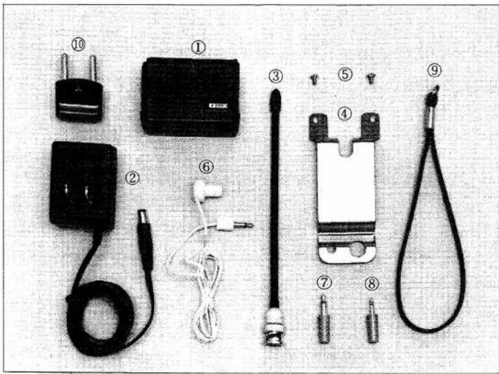
- Power pack IC-BP3 ..... 1
- Wall charger BC-25E ..... 1
- Flexible antenna ..... 1
- Belt clip. 1
- Belt clip retaining screws. . . . . . . 2
- Earphone.... 1
- Earphone plug .... 1
- Microphone plug..... 1
- Hand-strap.... 1
- AC conversion plug (Universal type) 1
SECTION IV PRE-OPERATION
BATTERY INSTALLATION
When using Nickel-Cadmium power pack IC-BP3:
The IC-BP3 is a rechargeable Nickel-Cadmium power pack, and it can be slipped onto or off the set very easily. It has a connector for a charger, charge-current control circuit, reverse polarity protection circuit and charge indicator LED in its own pack. You can use the supplied BC-25E wall charger or similar simple wall charger, or a car battery by using optional cable IC-CP1 for recharging. Before use, the power pack should be charged about 15 hours, because the battery may have discharged.
After charging is completed, the batteries can be used in the same manner as dry cells. However, the voltage of Nickel-Cadmium batteries drops rapidly just before they are exhausted, so when the Transmit Indicator LED of the transceiver goes out, be sure to immediately stop using it, and recharge the batteries again.
HOW TO CHARGE (When using Nickel-Cadmium power pack IC-BP3)
- Use the supplied wall charger BC-25E or a stable power source with an output voltage of DC 13.8V and current capacity over 50mA, or use a 12V car battery with optional charger cable IC-CP1. (Output voltage of 12 \~ 15V can be used, but output voltage near the specified voltage should be used.)
-
The power switch of the transceiver must be OFF, or remove the power pack from the transceiver.
-
Connect the output plug of the wall charger (BC-25E), or other power source, to the charger socket of the power pack. (When charging Nickel-Cadmium batteries in the IC-BP4 power pack, you should use the BC-30 charger only.)
The charge indicator LED of the power pack is lit, which shows that the charger is working.
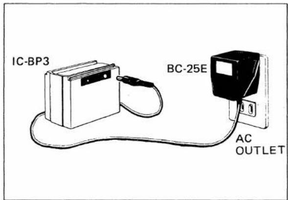
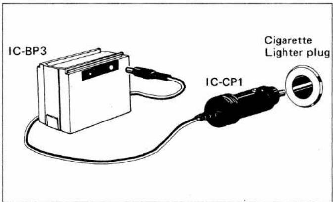
- It takes about 15 hours to charge the batteries completely. This charger is designed for 0.1C (10-hour rate current), but charge for 15 hours in order to compensate for any unbalance of the batteries.
You should charge the batteries for 15 hours when you have not used them for a long time or after buying them.
-
Charge between 0^ C and 40^ C.
-
Avoid continuing charging as much as possible after full charging, (15 hours). If excess charging is repeated, efficiency of the power pack is reduced.
-
After charging, unplug the power source from the charger socket of the power pack. The transceiver and the power pack are now ready for operation.
When using the alkaline power pack IC-BP4:
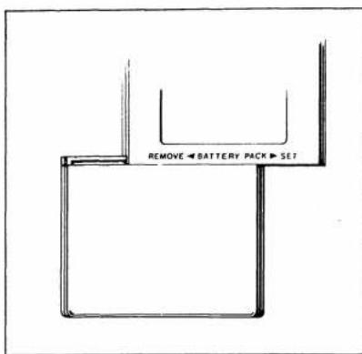
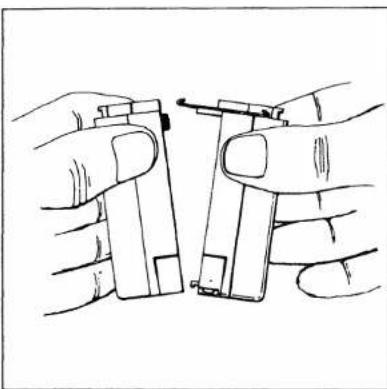
Place the power switch in the OFF position. Remove the power pack from the bottom of the set by pushing the pack in the indicated direction. Separate the pack into two parts (cases) as follows:
natural_image
Line drawing of two hands holding a small object, possibly a tool or device (no text or symbols present)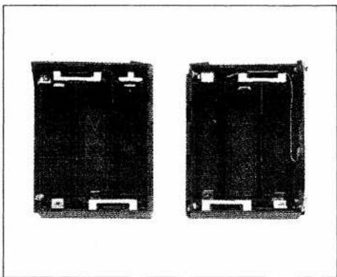
natural_image
Two black rectangular electronic components with mounting holes and circuit breakers, shown from front and side views (no text or symbols visible)Each case holds three AA type batteries. Install batteries into each case, according to indicated polarity. With the batteries properly in place, carefully replace the pack and slip it onto the set with the reverse procedure.
Also, AA type Nickel-Cadmium, rechargeable, batteries can be used. But the charger for them should be the optional BC-30 charger.
WHEN TO REPLACE BATTERIES (When using alkaline batteries)
When the Transmit Indicator LED does not light up during transmission, the batteries are exhausted. Use batteries of the same type, for mixed types might cause leakage. Replace worn batteries with a complete new set. If used with old batteries, the life of new ones might be shortened. Battery life is
shortened more by transmitting than by receiving, since several times more current is drawn during transmission. To prolong battery life, therefore, practice the following:
* Try to minimize the transmit period.
* Reduce volume during reception.
* Be sure to cut off power source when set is not used.
More working hours are available if high-performance batteries are employed.
FOR OUTDOOR USE
- Attach the supplied power pack. (Refer to "BATTERY INSTALLATION")
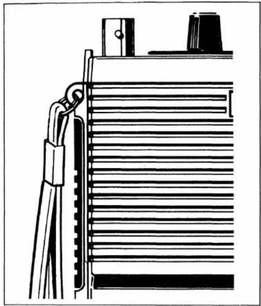
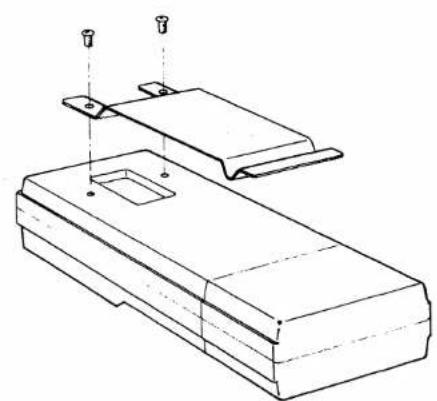
- Attach the supplied hand strap and belt clip through the fixture on the body (as shown in the drawings on page 9).
- Attach the flexible rubber antenna.
FOR USE IN A CAR
- Avoid using the unit near the outlet of heaters, air-conditioners, etc.
- Put the unit in a convenient place to avoid disrupting safe driving.
- Firmly ground to the car body a mobile antenna (e.g. whip antenna).
FOR FIXED USE
- Avoid putting the unit in places exposed to rain, water splash, direct sunshine, dust, vibration, or heat.
- An external antenna should be used for indoor operation. The use of the flexible antenna indoors may cause TVI, BCI, Hi-Fi interference or a malfunction stabilized DC power supply.
EXTERNAL ANTENNA
- Select a high performance antenna (a multi-element beam or gain antenna) and set it up in the highest possible position.
- Use a 50 ohm antenna and coaxial cable.
- On UHF, the power loss in the antenna cable is large, so use a cable with the lowest possible loss and make it as short as possible.
- Use a BNC plug for connection to the unit.
ATTACHMENT OF HAND STRAP AND BELT CLIP
natural_image
Technical line drawing of a mechanical component with no visible text or symbols- Attach the belt clip on the back cover with the 2 screws supplied.
natural_image
Technical line drawing of a mechanical part with mounting holes and a rectangular base (no text or symbols)SECTION V CONTROL FUNCTIONS
TOP PANEL
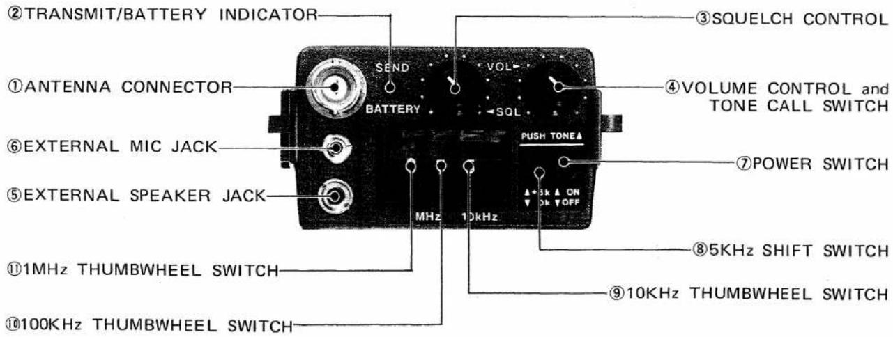
① ANTENNA CONNECTOR
Connect the supplied flexible antenna. An external antenna can be used, using a BNC connector.
② TRANSMIT/BATTERY INDICATOR
Illuminates in the transmit mode. Also indicates the battery condition; during transmission. The voltage of Nickel-Cadmium batteries drops rapidly just before they are exhausted, so when this indicator goes out, be sure to immediately stop using it, and charge the batteries again.
③ SQUELCH CONTROL
Sets the squelch threshold level. To turn OFF the squelch function, rotate this control completely counterclockwise. To set the threshold level higher, rotate the control clockwise.
④ VOLUME CONTROL and TONE CALL SWITCH
Controls the audio output level in the receive mode. Clockwise rotation increases audio output. Most repeaters require a 1750Hz Tone-burst for initial access. Depressing the VOLUME CONTROL knob for the required period for a repeater, puts the set in the transmit mode and the tone burst generator actuates and you can access the repeater.
⑤ EXTERNAL SPEAKER JACK
When an external speaker (or an earphone) is used, connect it to this jack. Use a speaker with an impedance of 8 ohms. When the external speaker is connected the built-in speaker does not function.
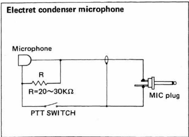
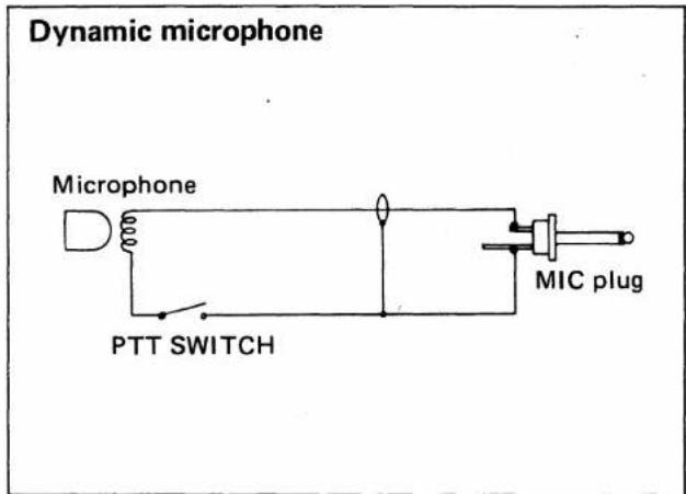
⑥ EXTERNAL MIC JACK
When an external microphone is used, connect it to this jack. See the schematic for the proper
hookup. When the external microphone is connected the built-in microphone does not function. The IC-HM9 optional speaker-microphone can also be used.
⑦ POWER SWITCH
The ON/OFF switch controls the supplied power to the set.
⑧ 5KHz SHIFT SWITCH
When the desired operating frequency has a 5KHz digit, set this switch in the +5KHz position, and add 5KHz to the indicated frequency on the thumbwheel switches.
⑨ 10KHz THUMBWHEEL SWITCH
Sets 10KHz digit of the desired operating frequency.
⑩ 100KHz THUMBWHEEL SWITCH
Sets 100KHz digit of the desired operating frequency.
⑪ 1MHz THUMBWHEEL SWITCH
Sets 1MHz digit of the desired operating frequency. When you set a digit of a frequency, the set will work as follows:
| Digit | Working frequency band |
| 0 | 430MHz |
| 1 | 431MHz |
| 2 | 432MHz |
| 3 | 433MHz |
| 4 | 434MHz |
| 5 | 435MHz |
| 6 | 436MHz |
| 7 | 437MHz |
| 8 | 438MHz |
| 9 | 439MHz |
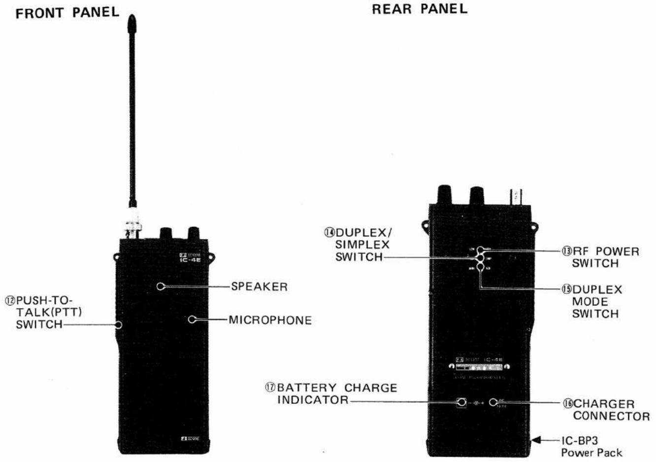
⑫ PUSH TO TALK (PTT) SWITCH
For transmission, press this switch and talk into the microphone with normal voice. The internal microphone is of the electret-condenser type and provides good pickup for all levels of voice.
⑬ RF POWER SWITCH
Selects the RF output power HIGH 1.5 Watts (at 8.4V) or LOW 0.15 Watts (at 8.4V). In the LOW position, the current drain is decreased, to prolong the battery life.
⑭ DUPLEX/SIMPLEX SWITCH
Selects the operation mode DUPLEX for repeater operation, or SIMPLEX for the same receive/ transmit frequency operation.
⑮ DUPLEX MODE SWITCH
In the DUPLEX mode, selects the transmitting frequency, 7.6MHz below (Version G: 1.6MHz above) the receiving frequency according to the desired repeater input frequency.
NOTE: The receiving frequency and transmitting frequency are shifted by the DUPLEX/SIMPLEX switch and DUPLEX MODE switch as follows:
The receiving frequency is shifted 7.6MHz below (Version G: 1.6MHz above) the displayed frequency, when the DUPLEX MODE switch is in the MONI POSITION.
The transmitting frequency is shifted 7.6MHz below (Version G: 1.6MHz above) the displayed frequency, when the DUPLEX/SIMPLEX switch is in the DUP position.
(Version SM: The DUPLEX MODE switch switches that the transmitting frequency is shifted 1.6MHz below or 4.6MHz below the displayed frequency when the DUPLEX/SIMPLEX switch is in the DUP position.)
⑯ CHARGER CONNECTOR
Connects to the output plug of the wall charger BC-25E or other power source.
⑰ BATTERY CHARGE INDICATOR
Lights during battery charging.
SECTION VI OPERATION
RECEIVING
Make sure the ⑦ POWER SWITCH is in the OFF position, and before turning ON the power switch, confirm as follows:
- Make sure the power pack is properly charged and attached to the set.
- Make sure the supplied flexible antenna is properly set.
When an external antenna is employed, make sure the coaxial line is of the correct impedance (50 ohms) and is neither shorted nor opened, and is firmly connected to the antenna connector.
Set the controls and switches as follows:
③ SQUELCH CONTROL Completely counterclockwise
④ VOLUME CONTROL Completely counterclockwise
⑨~⑪ THUMBWHEEL SWITCHES Desired frequency
(Others may be at any position or setting.)
Set the ⑦ POWER switch to the ON position.
Turn the ④ VOL control clockwise to a comfortable audio level.
If only noise can be heard and no signal, turn the ③ SQL control clockwise until the noise from the speaker stops and set it just below this threshold. (When adjusting the SQL setting, if some communication signals can be heard, turn the thumbwheel switch either direction and set it where only noise can be heard.) Your transceiver will now remain silent until an incoming signal is received which opens the squelch. If the squelch is unstable due to the reception of weak or mobile stations, adjust the squelch control further until the proper threshold is obtained.
TRANSMITTING
Set the controls and switches as follows:
⑭ DUPLEX/SIMPLEX SWITCH (see below)
⑮ DUPLEX MODE SWITCH (see below)
⑬ RF POWER SWITCH HIGH
For simplex operation, set ⑭ DUPLEX/SIMPLEX SWITCH at the SIMPLEX position, making ⑮ DUPLEX MODE SWITCH nonfunctional.
For repeater operation, set ⑭ DUPLEX/SIMPLEX SWITCH at DUPLEX and ⑮ DUPLEX MODE at NOR positions. (Version SM: -1.6 or -4.6 according to the repeater's input/output frequencies.)
The receiving and transmitting frequencies will be shifted by the DUPLEX/SIMPLEX switch and DUPLEX MODE switch as follows:
| DUP/SIMP DUPLEX MODE | SIMP | DUP |
| NOR | R: Displayed frequencyT: Displayed frequency | R: Displayed frequencyT: Display -7.6MHz |
| MONI | R: Display -7.6MHzT: Displayed frequency | R: Display -7.6MHzT: Display -7.6MHz |
(Version G)
| DUP/SIMP DUPLEX MODE | SIMP | DUP |
| NOR | R: Displayed frequencyT: Displayed frequency | R: Displayed frequencyT: Display +1.6MHz |
| MONI | R: Display +1.6MHzT: Displayed frequency | R: Display +1.6MHzT: Display +1.6MHz |
(Version SM)
| DUP/SIMP DUPLEX MODE | SIMP | DUP |
| -1.6 | R: Displayed frequencyT: Displayed frequency | R: Displayed frequencyT: Display -1.6MHz |
| -4.6 | R: Displayed frequencyT: Displayed frequency | R: Displayed frequencyT: Display -4.6MHz |
If the lower output power is sufficient, set ⑬ RF Power Switch to the LOW position.
Depress the ⑫ PTT switch for transmitting and release for receiving. Speak into the microphone with your normal speech level for the proper microphone level.
If you need a tone-burst for initial access of the repeater, depress the ④ Tone Call Switch for the required period. (Tone-burst periods vary individually from 100 milliseconds to 2 seconds.)
SECTION VII INSIDE VIEW
MAIN UNIT SIDE
Thumbwheel Switches
RX Band-Pass Filter-
FI1 (21.8MHz Crystal Filter)
RX Band-Pass Filter-
S1 (PTT Switch)
F12 (455KHz Ceramic Filter)
X1 (21.345MHz 2nd LO Crystal)
X2 (7.168MHz Tone-Burst Crystal)
IC3 (TC5082 Tone-Burst Generator)
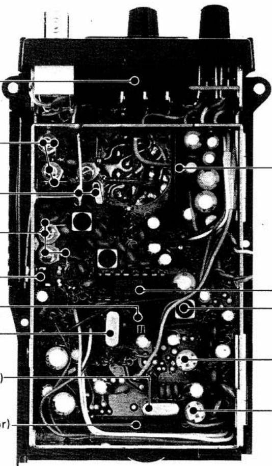
IC2 (BA526 AF Power Amp)
IC1 (MC3357 IF Circuit IC)
L8 (Quadrature Coil)
R83 (Tone Signal Level Adjust)
R82 (Deviation Adjust)
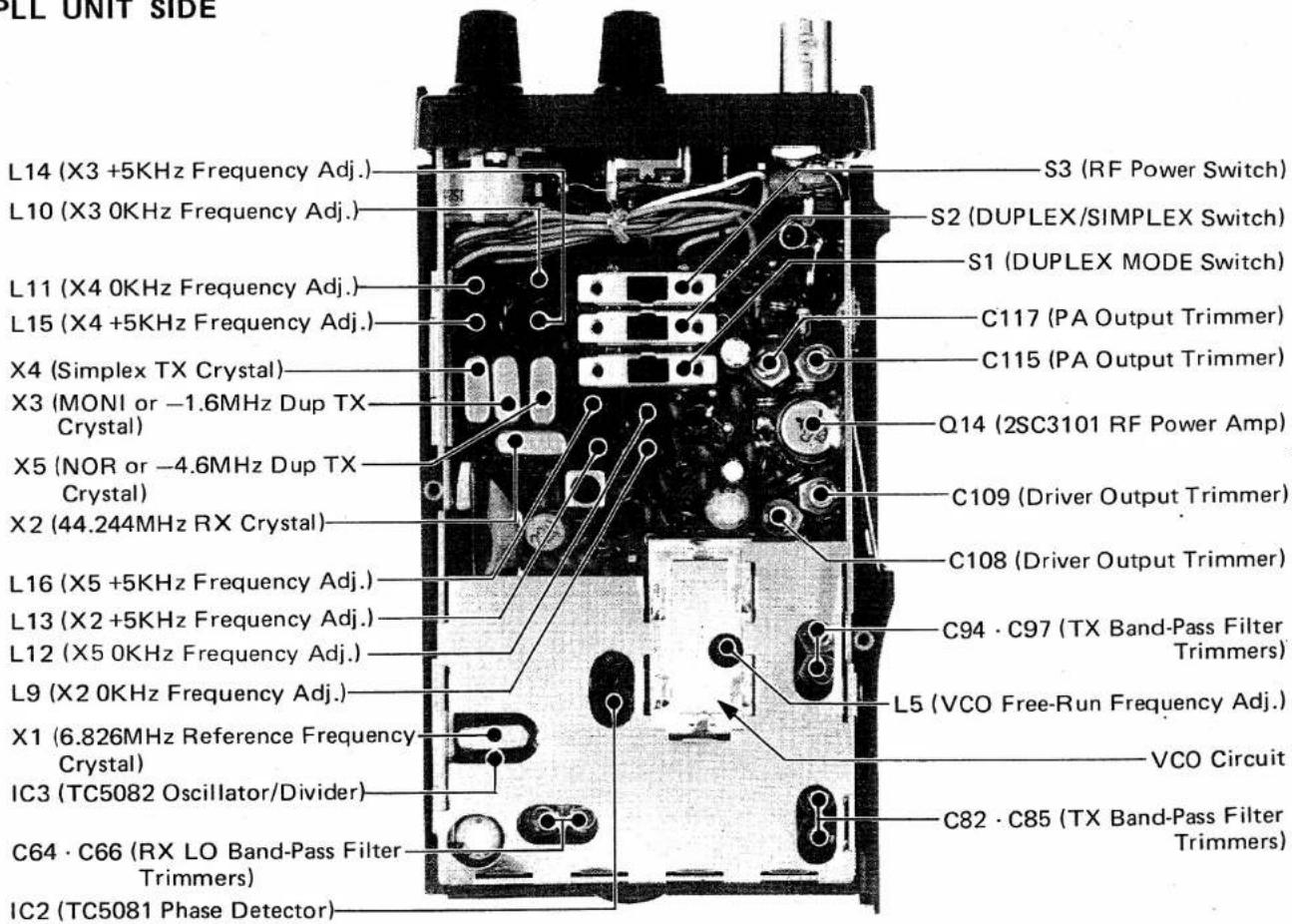
PLL UNIT SIDE
SECTION VIII CIRCUIT DESCRIPTION
RECEIVER CIRCUITS
ANTENNA SWITCHING CIRCUIT
Signals from the antenna connector are fed to the antenna switching circuit through low-pass filter consisting of C1, L1 C4, and L32 and C123 in the PLL board.
The antenna switching circuit employs a quater wave switching circuit.
In the receive mode, switching diodes, D16 and D17 are turned OFF, and they make isolation against the transmitter circuit and matching circuit, and the incoming signals are fed to the RF amplifier through L31.
RF AMPLIFIER AND FIRST MIXER
The signals from the switching circuit are fed to the cascode amplifier Q1 and Q2.
The amplified signals are fed to the base of the first mixer Q3 through the band-pass filter L2 \~ L5, which reduces interference and intermodulation from out of the band signals.
To the base of Q3, a 408MHz signal is supplied from the PLL circuit to convert the RF signals into 21.8MHz first IF signals. The first IF signals are taken from the collector of Q3 and fed to the IF circuit.
IF CIRCUIT
The first IF signals from Q3 are fed to the matched pair crystal filter F11, then IF amplifiers Q4 \~ Q6.
The amplified signals are fed to IC1. IC1 is composed of the second local oscillator, second mixer, limiter amplifier, quadrature detector and active filter circuits.
The second local oscillator oscillates 21.345MHz with X1, and is fed to the second mixer with the first IF signals to convert into 455KHz second IF signals. The second IF signals are put out from Pin 3, and fed to external ceramic filter FI2 which has excellent selectivity, then fed to IC1 (Pin 5) again to amplify and detect.
The detected AF signals are put out from Pin 9.
AF AND SQUELCH CIRCUITS
The detected AF signals are put 6dB/Octave de-emphasis by integral circuit consisting of R22 and C47, and fed to AF power amplifier IC2 through the VOLUME control R1, to obtain enough power to drive the speaker.
Noise components put out from Pin 9 of IC1 are fed to IC1 (Pin 10) again through the SQUELCH control R2, which controls the squelch threshold level, filtered about 20KHz signal (noise) and put out from Pin 11.
This signal (noise) is rectified by Q14, integrated by R39, R40 and C51, and turns Q15 ON and turns OFF the regulator for AF power amplifier consisting of D4, Q16 and Q17.
This reduces the current drain of the set, in the standby condition. When a signal is received, noise is suppressed by the signal and turns Q15 OFF and the regulator is turned ON and supplies regulated voltage to the AF power amplifier, and incoming signal can be heard from the speaker.
In the transmit mode, a voltage is applied to Q15 and turns it ON, and turns the regulator OFF the same as in the standby condition.
TRANSMITTER CIRCUITS
MIC AMPLIFIER CIRCUIT
Audio signals from the microphone are fed to the limiter amplifier, consisting of Q29 \~ Q32, which has 6dB/Octave response between 300Hz and 3KHz.
The output of the limiter amplifier is similar to rectangular waves and includes harmonics. These harmonics are eliminated by the low-pass filter Q33, which cuts 3KHz or higher. Filtered signals are fed to the VCO in the PLL board to make modulation.
MULTIPLIER AND DRIVER CIRCUITS
The VCO oscillates a third of a transmitting frequency, thus the multiplier Q10 and Q11, multiplies it three times to obtain 430MHz transmitting frequency.
This 430MHz signal is fed to amplifiers Q12 and Q13 through band-pass filter L22, L23 and L24, L25 to obtain 500 milliwatts pure 430MHz signal. While switching over receive to transmit, Q9 is turned ON by the charged voltage of C23, until the charged voltage has been discharged, and this function cuts the bias voltage of Q11 \~ Q14.
This prevents transmission of unwanted signals.
POWER AMPLIFIER CIRCUIT
The output signals from Q13 is fed to the power amplifier Q14, and amplified to 1.5 watts. In the transmit mode, D16 and D17 are turned ON, and D17 makes L31 have high-impedance and D16 feeds the signals to the antenna through the low-pass filter.
PLL CIRCUITS
LOCAL OSCILLATOR CIRCUIT
The crystal oscillator Q7 oscillates 44.245MHz with X2 for receive, 43.400MHz (Version G: 44.422 MHz) with X3 for receive in MONI mode (Version SM: 46.489MHz with X3 for -1.6MHz duplex transmit), 46.667MHz with X4 for simplex transmit, 45.822MHz with X5 for -7.6MHz duplex transmit (Version G: 46.844MHz with X5 for +1.6MHz duplex transmit, Version SM: 46.155MHz with X5 for -4.6MHz duplex transmit), and the signal at three times this frequency is taken from the collector of Q7, and fed to the mixer of the PLL circuit.
In the receive "NOR" mode, R+5V is applied to D8 through R23, L9, L13 and R27, and D8 is turned ON and selects X2.
In the simplex transmit mode, T+5V is applied to D10 through R25, L11, L15 and R29, and D10 is turned ON and selects X4.
In the -7.6MHz (Version G: +1.6MHz, Version SM: -1.6MHz) duplex transmit mode, T+5V is applied to D11 through R60, L12, L16 and R58, and D11 is turned ON and selects X5.
In the "MONI" mode, R+5V (Version SM: In the -4.6MHz duplex transmit mode, T+5V) is applied to D9 through R24, L10, L14 and R28, and D9 is turned ON and selects X3.
When the operating frequency has a 5KHz digit, cathodes of D4 \~ D7 are grounded through the 5KHz SHIFT switch, and one of D4 \~ D7 is turned ON according to the operating mode. Thus, one of L9 \~ L12 is shunted accordingly and oscillating frequency is shifted 5KHz (on the operating frequency).
MIXER, LOW-PASS FILTER AND AMPLIFIER CIRCUITS
The output signals from the local oscillator circuit and the VCO signals fed through buffer amplifiers Q3 and Q4 are mixed by the mixer Q5. The output signals are fed to the low-pass filter to filter out only the signals below 7MHz, then fed to Q6 to be amplified to proper drive level (more than 3Vp-p) of the programmable divider IC1.
PROGRAMMABLE DIVIDER CIRCUIT
The input signals at Pin 2 of IC1 are divided by the BCD input signals from the thumbwheel switches at Pin 3 \~ 14.
REFERENCE FREQUENCY GENERATOR CIRCUIT
Reference frequency generator IC3 consists of a crystal oscillator and a highspeed divider. X1 oscillates at 6.8266MHz, which is divided by 2048. The 10/3KHz reference frequency is fed to phase detector IC2. This 10/3KHz reference frequency decides the variation step of the PLL output frequency.
PHASE DETECTOR AND LOOP FILTER CIRCUITS
Digital phase detector, IC2, detects the phase difference of the pulse signals of the 10/3KHz reference frequency and the output signal of the programmable divider, and proportionately puts out pulse signals at Pin 3, which becomes high impedance when the PLL is locked.
Pin 4 is for detecting the lock failures and changes to ground level according to the phase difference of the two pulse signals. When the lock fails, the pulse signal from Pin 4 is integrated by R10 and C14. When the integrated voltage exceeds the junction voltage of Q9's base in the MAIN board, Q9 is turned ON and then Q8 in the MAIN board is turned ON.
The collector of Q8 is connected to the base of Q7, so the base voltage of Q7 becomes ground level, and Q7 is shut off to prevent transmitting unwanted signals.
The loop filter, consisting of R3 \~ R5, C15 and C16, converts the pulse signal from Pin 3 into a DC voltage and decides the response time of the whole loop.
The output signals are fed to tuning diode D1 of the VCO circuit as the control voltage for the VCO frequency set.
VCO CIRCUIT
The VCO (Voltage-Controlled Oscillator) is a Colpitts circuit using Q2, and oscillates in 130 \~ 140MHz range.
The oscillator frequency is controlled by a DC voltage which is supplied from the loop filter to varactor diode D1.
In the receive mode, R+5V is applied to D2's anode through L3, and D2 is turned ON and shunts C23. Thus the free-run frequency of the VCO is lowered.
In the transmit mode, T+5V is applied to D2's cathode through D3 and L4, D2 is turned OFF, and C23 is inserted in the oscillator circuit in series. Thus the free-run frequency of the VCO is increased. In the same time, the VCO signal is frequency modulated by the audio signals from the microphone which are applied to the gate of Q2 and varies Q2's mutual conductance.
POWER SUPPLY CIRCUIT
The regulated 5V is supplied to the main circuits, so that the set operates under a stable condition with as a lower voltage as possible.
The power supply voltage is fed to the AF power amplifier through the squelch switching circuit and to the 5V regulator consisting of Q20 \~ Q23 and zener diode D5. This regulated 5V is supplied to the PLL circuit.
In the transmit mode, the base of Q26 is grounded through R63, the microphone and the PTT switch, and Q26 is turned ON. Thus Q7 and Q8 are turned ON and T+5V is actuated, and supplied to the transmitter circuit. At the same time, T+5V turns Q13 ON, and the power supply voltage is applied to the MIC amplifier circuit through Q13.
In the receive mode, Q26 is turned OFF and the bias voltage of Q10 ON. Thus the R+5V is actuated and supplied to the PLL board to switch the local oscillator crystal and the driver transistors of the transmitter circuit.
At the same time, R+5V turns ON the voltage boost circuit consisting of Q12 and Q11, and +6V is supplied to the receiver circuit.
LED INDICATOR CIRCUIT
This LED is lit in the transmit mode, but when the power supply voltage becomes less than 5.5V, it will not be lit.
The power supply voltage is divided by R57 and R58, and applied to the base of Q24. The emitter of Q24 is connected to the regulated 5V source. When the power supply voltage is more than 5.5V, Q24 is turned OFF, Q25 is turned ON and T+5V is applied to the LED through Q25 and R56, and LED is lit.
TONE-BURST GENERATOR CIRCUIT
When the TONE CALL switch is depressed, Q26's base is grounded through R63 and D7, and the set is turned in the transmit mode. At the same time, Q34's base is also grounded through R84, and Q34 is turned ON and supplies a voltage to IC3.
IC3 consists of a crystal oscillator and dividers. X2 oscillates at 7.168MHz, which is divided by 4096.
The 1750Hz tone is put out from Pin 4 of IC3 and fed to the mic amplifier circuit through R83, level adjust trimmer.
SECTION IX TROUBLE-SHOOTING
Your IC-4E has been tested very carefully at the factory before shipping. The chart below has been designed to help you correct any problems which are not equipment malfunctions. If you are not able to locate the problem and/or solve it through use of this chart, please contact your dealer or ICOM distributor for assistance.
| Problem | Possible Cause | Solution |
| 1. Power does not come ON when the switch is turned. | Bad connection of the power pack.Reverse polarity of the battery (when using IC-BP4).The battery has been exhausted. | Check the connection of the power pack and correct any problems.Make sure of the polarity of each battery and replace them into the pack.Replace the battery with a new one or recharge it. |
| 2. No sound comes from the speaker. | VOLUME CONTROL knob is completely counterclockwise.The unit is in the transmit mode, by the PTT switch. | Turn the knob clockwise to a suitable level.Put the unit in the receive mode. |
| 2. No sound comes from the speaker.(Continued) | SQUELCH setting is turned too far clockwise.External speaker (or earphone) is in use.The battery has been exhausted. | Turn the SQUELCH CONTROL counterclockwise until noise can be heard and reset it just below the threshold.Check if the external speaker plug is inserted properly or if the external speaker cable is cut.Replace the battery with a new one or recharge it. |
| 3. Sensitivity is low and only strong signals are audible. | Bad connection of the flexible antenna.The antenna feed line is cut or shorted. (When using an external antenna.) | Check the connection of the antenna and correct any problems.Check the feed line and correct any improper condition. |
| 4. No or low RF output. | RF Power switch is set at the Low position.The battery has been exhausted. | Set the RF Power switch to the High position.Replace the battery with a new one or recharge it. |
| 4. No or low RF output.(Continued) | The antenna feed line is cut or shorted. (When using an external antenna.) | Check the antenna feed line and correct any problems. |
| 5. No modulation.(When using external microphone.) | Bad connection of the MIC connector.The MIC cable is cut. | Check the connection of the MIC connector and correct any problems.Repair the disconnected or cut wire. |
| 6. The receive mode functions properly and your signals are transmitted, but you are unable to make contact with another station. (When desiring DUPLEX mode.)(When desiring, SIMPLEX mode.) | The DUPLEX/SIMPLEX Switch is in the SIMP position.Improper input/Output frequency of the repeater.The DUPLEX/SIMPLEX Switch is in the DUP position.The DUPLEX MODE switch is in the MONI position. | Set the DUPLEX/SIMPLEX Switch in the DUP position, and the DUPLEX MODE switch in NOR (Version SM: -1.6 or -4.6) position according to repeater input/output frequencies.Set the DUPLEX/SIMPLEX Switch in the SIMP position.Set the DUPLEX MODE Switch in the NOR position. |
SECTION X VOLTAGE CHARTS
NOTE: Measuring instrument is a 50KΩ/V multimeter.
MAIN UNIT TRANSISTORS
| TR No. | TRANSMIT | RECEIVE | REMARKS | ||||||
| BASE OR GATE1 | GATE2 | COLLECTOR OR DRAIN | EMITTER OR SOURCE | BASE OR GATE1 | GATE2 | COLLECTOR OR DRAIN | EMITTER OR SOURCE | ||
| Q 1 | 0 | 0 | GND | 0.75 | 2.0 | GND | |||
| Q 2 | 0 | 0 | 0 | 3.0 | 3.4 | 2.2 | |||
| Q 3 | 0 | 0 | GND | 0.7 | 4.0 | GND | |||
| Q 4 | 0 | 0 | 0 | 1.7 | 1.7 | 1.0 | |||
| Q 5 | 0 | 0 | 0 | 1.0 | 1.7 | 0.4 | |||
| Q 6 | 0 | 0 | 0 | 1.7 | 4.4 | 2.4 | |||
| Q 7 | 0 | 4.8 | 5.0 | 4.8 | 0 | 5.0 | |||
| Q 8 | 0 | 0 | GND | 0.3 | 4.4 | GND | |||
| Q 9 | 0 | 0 | GND | 0 | 0.3 | GND | |||
| Q10 | 4.6 | 0 | 5.0 | 4.2 | 5.0 | 5.0 | |||
| Q11 | 8.4 | 0 | 9.0 | 8.4 | 6.0 | 9.0 | |||
| Q12 | 0 | 8.0 | 0 | 5.0 | 8.0 | 4.0 | |||
| Q13 | 5.0 | 8.4 | 4.0 | 0 | 9.0 | 2.8 | |||
| Q14 | 0 | 0 | 0 | 4.0 | 0/1.7 | 3.8/3.0 | SQL OFF/ON | ||
| Q15 | 0 | 0 | GND | 0/0.6 | 8.0/0 | GND | SQL OFF/ON | ||
| Q16 | 0 | 8.4 | 0 | 8.0/0 | 8.4 | 7.6/0 | SQL OFF/ON | ||
| Q17 | 8.4 | 0 | 9.0 | 8.4 | 7.6/0 | 9.0 | SQL OFF/ON | ||
| Q18 | - | - | - | - | - | - | Deleted | ||
| Q19 | - | - | - | - | - | - | Deleted | ||
| Q20 | 0.6 | 9.0 | 1.3 | 0.5 | 9.0 | 1.3 | |||
| Q21 | 8.2 | 5.0 | 9.0 | 8.4 | 5.0 | 9.0 | |||
| Q22 | 0.6 | 8.1 | GND | 0.5 | 8.3 | GND | |||
| Q23 | 0.6 | 0.6 | GND | 0.6 | 0.5 | GND | |||
| Q24 | 5.7 | 3.4 | 5.0 | 5.8 | 0 | 5.0 | |||
| Q25 | 3.4 | 4.0 | 4.0 | 0 | 0 | 0 | |||
| Q26 | 4.8 | 3.8 | 5.0 | 3.7 | 1.3 | 5.0 | |||
| Q27 | 0 | 3.6 | GND | 0.6 | 5.0 | GND | |||
| Q28 | 0 | 0.6 | GND | 0 | 0 | GND | |||
| Q29 | 1.5 | 4.0 | 2.0 | 0 | 0 | 0 | |||
| Q30 | 2.1 | 3.4 | 2.0 | 0 | 0 | 0 | |||
| Q31 | 3.4 | 1.8 | 4.0 | 0 | 0 | 0 | |||
| Q32 | 0.6 | 0.7 | GND | 0 | 0 | GND | |||
| Q33 | 0.7 | 4.0 | 1.9 | 0 | 0 | 0 | |||
| Q34 | 3.6 | 4.0 | 4.0 | 0 | 0 | 0 | |||
| Q35 | 0 | 0 | GND | 0.7 | 0 | GND | |||
PLL UNIT TRANSISTORS
| TR No. | TRANSMIT | RECEIVE | REMARKS | ||||||
| BASE OR GATE1 | GATE2 | COLLECTOR OR DRAIN | EMITTER OR SOURCE | BASE OR GATE1 | GATE2 | COLLECTOR OR DRAIN | EMITTER OR SOURCE | ||
| Q 1 | — | — | — | — | — | — | Deleted | ||
| Q 2 | 0 | 4.0 | 0.6 | 0 | 4.0 | 0 | |||
| Q 3 | 0.7 | 0.7 | GND | 0.7 | 0.7 | GND | |||
| Q 4 | 1.8 | 2.8 | 0.7 | 1.8 | 2.8 | 0.7 | |||
| Q 5 | 0.7 | 0.75 | GND | 0.7 | 0.75 | GND | |||
| Q 6 | 1.4 | 3.2 | 1.0 | 1.4 | 3.2 | 1.0 | |||
| Q 7 | 1.6 | 5.0 | 1.0 | 1.6 | 5.0 | 1.0 | |||
| Q 8 | 0 | 0 | 1.2 | 1.7 | 5.0 | 1.3 | |||
| Q 9 | 0 | 1.3 | GND | 0.6 | 0 | GND | |||
| Q10 | 0.5 | 1.3 | GND | 0.4 | 0.8 | GND | |||
| Q11 | 1.3 | 4.0 | 0.5 | 0 | 0 | 0 | |||
| Q12 | 1.2 | 8.5 | 0.5 | 0 | 9.0 | 0 | |||
| Q13 | 0.5/0.7 | 9.0 | 0.3/1.5 | 0 | 9.0 | 0 | Power Hi/Low | ||
| Q14 | 0.3/0.5 | 9.0 | GND | 0 | 9.0 | GND | Power Hi/Low | ||
IN TRANSMIT MODE
| UNIT | IC No. | PIN No. | REMARKS | |||||||||||||||||
| 1 | 2 | 3 | 4 | 5 | 6 | 7 | 8 | 9 | 10 | 11 | 12 | 13 | 14 | 15 | 16 | 17 | 18 | |||
| MAIN | IC1 | 0 | 0 | 0 | 0 | 0 | 0 | 0 | 0 | 0 | 0 | 0 | GND | 0 | 0 | 0 | 0 | |||
| MAIN | IC2 | 0 | 0 | 0 | 0 | GND | 0 | 0 | 0 | 0 | ||||||||||
| MAIN | IC3 | 0.8 | 1.4 | 1.6 | 1.8 | 4.0 | 2.0 | 2.0 | 2.0 | GND | ||||||||||
| PLL | IC1 | 5.0 | 2.0 | 0 | 0 | 0 | 0 | 0 | 0 | 0 | 0 | 0 | 0 | 0 | 0 | 5.0 | 0 | 0 | GND | f = 430MHz |
| PLL | IC2 | 5.0 | 0 | 1.2 | 5.0 | 5.0 | 0 | 0 | 2.4 | GND | ||||||||||
| PLL | IC3 | 1.0 | 2.0 | 2.4 | 2.4 | 5.0 | 2.4 | 2.4 | 2.4 | GND | ||||||||||
IN RECEIVE MODE
| UNIT | IC No. | PIN No. | REMARKS | |||||||||||||||||
| 1 | 2 | 3 | 4 | 5 | 6 | 7 | 8 | 9 | 10 | 11 | 12 | 13 | 14 | 15 | 16 | 17 | 18 | |||
| MAIN | IC1 | 5.2 | 5.2 | 5.4 | 5.8 | 0.9 | 0.9 | 1.1 | 5.8 | 2.9 | 1.7 | 2.2 | GND | 5.1 | 0 | GND | 2.0 | |||
| MAIN | IC2 | 6.1 | 4.0 | 7.6 | 3.4 | GND | 3.2 | 3.2 | 3.2 | 3.2 | SQL OPEN | |||||||||
| MAIN | IC3 | 0 | 0 | 0 | 0 | 0 | 0 | 0 | 0 | GND | ||||||||||
| PLL | IC1 | 5.0 | 1.6 | 0 | 0 | 0 | 0 | 0 | 0 | 0 | 0 | 0 | 0 | 0 | 0 | 5.0 | 0 | 0 | GND | f = 430MHz |
| PLL | IC2 | 5.0 | 0 | 1.2 | 5.0 | 5.0 | 0 | 0 | 2.4 | GND | ||||||||||
| PLL | IC3 | 1.0 | 2.0 | 2.4 | 2.4 | 5.0 | 2.4 | 2.4 | 2.4 | GND | ||||||||||
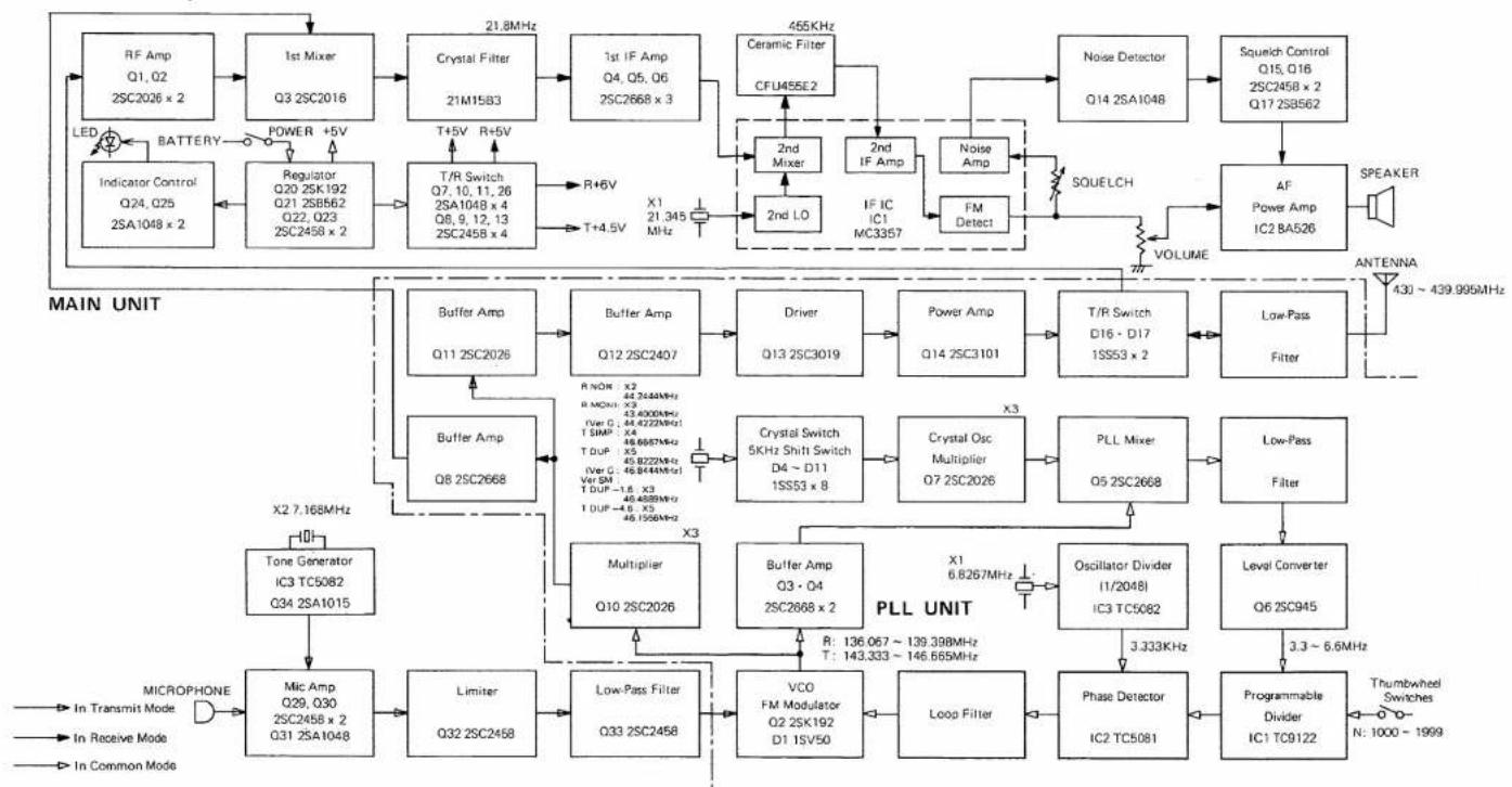
SECTION XI BLOCK DIAGRAM
flowchart
graph TD
    subgraph MAIN UNIT
        A["RF Amp Q1, Q2 2SC2026 x 2"] --> B["1st Mixer Q3 2SC2016"]
        C["Indicator Control Q24, Q25 2SA1048 x 2"] --> D["Regulator Q20 2SK192 Q21 2SB562 Q22, Q23 2SC2458 x 2"]
        B --> E["Crystal Filter 21M15B3"]
        D --> F["T/R Switch Q7, 10, 11, 26 2SA1048 x 4 Q8, 9, 12, 13 2SC2458 x 4"]
        E --> G["1st IF Amp Q4, Q5, Q6 2SC2668 x 3"]
        F --> H["T+5V R+5V"]
        G --> I["R+6V"]
        H --> J["T+4.5V"]
        I --> K["T+4.5V"]
        J --> L["X1 21.345 MHz"]
        K --> M["CFU455E2"]
        L --> N[" Ceramic Filter CFU455E2"]
        M --> O[" Ceramic Filter CFU455E2"]
        N --> P[" 2nd Mixer "]
        O --> Q[" 2nd Mixer "]
        P --> R[" 2nd LO "]
        Q --> S[" 2nd LO "]
        R --> T[" 2nd LO "]
        S --> U[" 2nd LO "]
        T --> V[" 2nd LO "]
        U --> W[" 2nd LO "]
        V --> X[" 2nd LO "]
        W --> Y[" 2nd LO "]
        X --> Z[" 2nd LO "]
        Y --> AA[" 2nd LO "]
        Z --> AB[" 2nd LO "]
        AA --> AC[" 2nd LO "]
        AB --> AD[" 2nd LO "]
        AC --> AE[" 2nd LO "]
        AD --> AF[" 2nd LO "]
        AE --> AG[" 2nd LO "]
        AF --> AH[" 2nd LO "]
        AG --> AI["SQUELCH"]
        AH --> AJ["SQUELCH"]
        AI --> AK["SQUELCH"]
        AJ --> AL["SQUELCH"]
        AK --> AM["SQUELCH"]
        AL --> AN["SQUELCH"]
        AM --> AO["SQUELCH"]
        AN --> AP["SQUELCH"]
        AO --> AQ["SQUELCH"]
        AP --> AR["SQUELCH"]
        AQ --> AS["SQUELCH"]
        AR --> AT["SQUELCH"]
        AS --> AU["SQUELCH"]
        AT --> AV["SQUELCH"]
        AU --> AW["SQUELCH"]
        AV --> AX["SQUELCH"]
        AW --> AY["SPEAKER"]
        AX --> AZ["SPEAKER"]
        BA["Power Amp IC2 BA526"] --> BB["AF Power Amp IC2 BA526"]
        BC["Lower Filter"] --> BD["Low-Pass Filter"]
        BE["Antenna"] --> BF["Antenna"]
        BG["Tone Generator IC3 TC5082 Q34 2SA1015"] --> BH["Mic AMP Q29, Q30 2SC2458 x 2 Q31 2SA1048"]
        BI["North Mode"] --> BJ["Limiter Q32 2SC2458"]
        BK["In Receive Mode"] --> BL["Mic AMP Q29, Q30 2SC2458 x 2 Q31 2SA1048"]
    end
    subgraph PLL UNIT
        BD --> BL
        BL --> BM["Multiplier Q10 2SC2026"]
        BM --> BN["Buffer Amp Q3 - Q4 2SC2668 x 2"]
        BN --> BO["Buffer Amp Q3 - Q4 2SC2668 x 2"]
        BP["VCO FM Modulator Q2 2SX192 D1 1SV50"] --> BQ["VCO FM Modulator Q2 2SX192 D1 1SV50"]
        BPQ["VCO FM Modulator Q2 2SX192 D1 1SV50"] --> BR["VCO FM Modulator Q2 2SX192 D1 1SV50"]
    end
    subgraph Programmable Divider IC1 TC9122
        BS["Programmable Divider IC1 TC9122"] --> BT["Thawbowl Switches N: 1000 ~ 1999"]
    end
    subgraph PLL UNIT
        BS --> BU["Tone Generator IC3 TC5082 Q34 2SA1015"]
    end
    subgraph MAIN UNIT
        CA["Power Amp Q11 2SC2026"] --> CB["Buffer Amp Q12 2SC2407"]
        CB --> CC["Buffer Amp Q13 2SC3019"]
        CC --> DC["Driver Q13 2SC3019"]
        DC --> ED["Power Amp Q14 2SC3101"]
        ED --> EF["T/R Switch D16 - D17 1SS53 x 2"]
        EF --> GF["Low-Pass Filter"]
        GF --> GH["Low-Pass Filter"]
    end
SECTION XII OPTIONS
We have prepared a variety of options for the transceiver IC-4E in order to expand its use.
1. BC-30 Nickel-Cadmium Battery Charger
A convenient set-in type charger for Nickel-Cadmium power packs. Two charging rates provided - high speed and regular rate. The charger is compatible with any type of Nickel-Cadmium power packs.
2. IC-BP2 Nickel-Cadmium Power Pack
This power pack has six AA type 400mAh Nickel-Cadmium batteries and provides 1W output power for the IC-4E with longer attendant use capability. Recharge time, when using the BC-30 is 1-1/2 hours.
3. IC-BP4 Battery Case
This case will accept dry batteries, zinc or alkaline, for 1.5W output, or Nickel-Cadmium for 1W output power. It holds six cells. When Nickel-Cadmium are installed the BC-30 can be used to recharge the batteries.
4. IC-BP5 Nickel-Cadmium Power Pack
This power pack has nine AA type 400mAh Nickel-Cadmium batteries and provides 2.3W output power, plus longer operating capability. It can be recharged by the BC-30 in 1-1/2 hours.
5. IC-CP1 Cigarette Lighter Recharger for IC-BP3
A handy way to recharge the Nickel-Cadmium packs while mobile - plugs in the cigarette lighter.
6. IC-HM9 Speaker/Microphone
A handy speaker and microphone in one unit. Clips on the clothing and operates as both speaker and microphone when plugged in the unit.

ICOM
ICOM INCORPORATED
1-6-19, KAMI KURATSUKURI, HIRANO-KU OSAKA JAPAN
A-0368
Printed in Japan
- IC-4E
- 430MHz FM TRANSCEIVER
- TABLE OF CONTENTS
- SECTION I INTRODUCTION
- SYNTHESIZED HAND HELD TRANSCEIVER
- DUAL POWER LEVEL
- VARIOUS POWER PACKS AVAILABLE
- HIGHLY EFFICIENT FLEXIBLE ANTENNA
- SECTION II SPECIFICATIONS
- SECTION III ACCESSORIES
- SECTION IV PRE-OPERATION
- BATTERY INSTALLATION
- When using Nickel-Cadmium power pack IC-BP3:
- HOW TO CHARGE (When using Nickel-Cadmium power pack IC-BP3)
- When using the alkaline power pack IC-BP4:
- WHEN TO REPLACE BATTERIES (When using alkaline batteries)
- FOR OUTDOOR USE
- FOR USE IN A CAR
- FOR FIXED USE
- EXTERNAL ANTENNA
- ATTACHMENT OF HAND STRAP AND BELT CLIP
- SECTION V CONTROL FUNCTIONS
- TOP PANEL
- SECTION VI OPERATION
- RECEIVING
- TRANSMITTING
- SECTION VII INSIDE VIEW
- MAIN UNIT SIDE
- PLL UNIT SIDE
- SECTION VIII CIRCUIT DESCRIPTION
- RECEIVER CIRCUITS
- ANTENNA SWITCHING CIRCUIT
- RF AMPLIFIER AND FIRST MIXER
- IF CIRCUIT
- AF AND SQUELCH CIRCUITS
- TRANSMITTER CIRCUITS
- MIC AMPLIFIER CIRCUIT
- MULTIPLIER AND DRIVER CIRCUITS
- POWER AMPLIFIER CIRCUIT
- PLL CIRCUITS
- LOCAL OSCILLATOR CIRCUIT
- MIXER, LOW-PASS FILTER AND AMPLIFIER CIRCUITS
- PROGRAMMABLE DIVIDER CIRCUIT
- REFERENCE FREQUENCY GENERATOR CIRCUIT
- PHASE DETECTOR AND LOOP FILTER CIRCUITS
- VCO CIRCUIT
- POWER SUPPLY CIRCUIT
- LED INDICATOR CIRCUIT
- TONE-BURST GENERATOR CIRCUIT
- SECTION IX TROUBLE-SHOOTING
- SECTION X VOLTAGE CHARTS
- SECTION XI BLOCK DIAGRAM
- SECTION XII OPTIONS
- BC-30 Nickel-Cadmium Battery Charger
- IC-BP2 Nickel-Cadmium Power Pack
- IC-BP4 Battery Case
- IC-BP5 Nickel-Cadmium Power Pack
- IC-CP1 Cigarette Lighter Recharger for IC-BP3
- IC-HM9 Speaker/Microphone
- ICOM INCORPORATED
Marke : ICOM
Modell : IC-4E
Kategorie : Empfänger