
IC-505 - Empfänger ICOM - Kostenlose Bedienungsanleitung
Finden Sie kostenlos die Bedienungsanleitung des Geräts IC-505 ICOM als PDF.


| Produkttyp | 50-MHz-SSB/CW/(FM)-Transceiver |
| Frequenzbereich | 50 bis 54 MHz |
| Betriebsmodi | A1 (CW), A3J (USB/LSB), F3 (FM optional) |
| Sendeleistung | 10 W (PA ein), 3 W (PA aus), 0,5 W (Low Power) |
| Stromversorgung | 13,8 V DC ±20 % (extern) oder 9 Mignon-Batterien (C) oder Ni-Cd-Akku IC-BP10 |
| Stromverbrauch (Empfang) | Max. 300 mA bei max. Lautstärke |
| Stromverbrauch (Senden) | Max. 2,9 A bei 10 W CW |
| Empfindlichkeit (SSB/CW) | 0,5 μV für 10 dB S+N/N |
| Empfindlichkeit (FM) | 0,6 μV für 20 dB Rauschsperre |
| Antennenimpedanz | 50 Ohm unsymmetrisch |
| Abmessungen (B×H×T) | 230 mm × 76 mm × 188,5 mm |
| Gewicht | 3,2 kg (mit Batterien) |
| Frequenzstabilität | Innerhalb ±1 kHz |
| Betriebstemperaturbereich | −10 °C bis +50 °C |
| Selektivität (SSB/CW) | ±1,1 kHz bei −6 dB; ±2,5 kHz bei −60 dB |
| Audio-Ausgangsleistung | Mehr als 1,5 W an 8 Ohm bei 10 % THD |
| Speicherkanäle | 6 (M1–M6) + CALL-Kanal |
| VFO-System | Dual VFO (A/B); VFO-Angleichung (A=B) |
| Scan-Funktionen | Speicher-Scan, Programm-Scan (zwischen M1 und M2) |
| Zusatzfunktionen | RIT (±1 kHz), Split-Betrieb, Rauschsperre (SQL), Rauschunterdrücker (NB), Rasttaste (Dial Lock), CW-Break-In |
| Stromversorgung für Speicher-Backup | 4 AA-Batterien (jährlicher Wechsel empfohlen) |
| Mitgeliefertes Zubehör | Mikrofon IC-HM7, Lautsprecherstecker, Tastenstecker, Gleichstromkabel, Schultergurt, 9 Mignon-Zellen, Ohrhörer |
| Empfohlene Optionen | Ni-Cd-Akku IC-BP10, FM-Modul IC-EX248, Netzteil IC-3PE, Tischmikrofon IC-SM5 |
Häufig gestellte Fragen - IC-505 ICOM
Benutzerfragen zu IC-505 ICOM
0 Frage zu diesem Gerät. Beantworten Sie die, die Sie kennen, oder stellen Sie Ihre eigene.
Eine neue Frage zu diesem Gerät stellen
Laden Sie die Anleitung für Ihr Empfänger kostenlos im PDF-Format! Finden Sie Ihr Handbuch IC-505 - ICOM und nehmen Sie Ihr elektronisches Gerät wieder in die Hand. Auf dieser Seite sind alle Dokumente veröffentlicht, die für die Verwendung Ihres Geräts notwendig sind. IC-505 von der Marke ICOM.
BEDIENUNGSANLEITUNG IC-505 ICOM
IC-505
50 MHz SSB CW (FM) TRANSCEIVER
OPERATION MANUAL
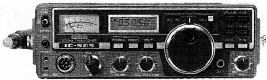
The IC-505 is a 50 MHz band SSB, CW (FM) transceiver developed by ICOM that engages the latest computer technology and high-precision VHF engineering.
In order to fully enjoy the complete benefits of this high performance transceiver, be sure to read and study this operation manual thoroughly before operation, and feel free to contact your authorized ICOM dealer to answer any questions you may have.
CONTENTS
I. SPECIFICATIONS.... 1
II. FEATURES 2
III. CONTROL FUNCTIONS.... 3
IV. BEFORE OPERATION 7
V. OPERATION GUIDE.... 13
VI. CIRCUIT OPERATION.... 15
VII. PRECAUTIONS.... 17
VIII. BASIC PARTS LAYOUT 18
IX. TROUBLESHOOTING GUIDE.... 19
X. BLOCK DIAGRAM.... 20
XI. ACCESSORIES AND OPTIONS 21
SECTION I SPECIFICATIONS
GENERAL
| Frequency coverage: | 50 to 54 MHz |
| Operating temperature range: | -10°C to +50°C(+15°F to +125°F) |
| Frequency stability: | Within ±1 kHz |
| Antenna impedance: | 50 ohms unbalanced |
| Operating voltage range: | 13.8V DC ±20% |
| Grounding: | Negative |
| Current consumption: | Receive Mode:250 mA max., at min. audio level300 mA max., at max. audio levelTransmit Mode:2.9 A max., at CW 10W output0.9 A max., at CW 3W output600 mA at CW low power (0.5W) |
| Dimensions: | 76 mm (H) × 230 mm (W) × 188.5 mm (D)(3.0" × 9.1" × 7.4") |
| Weight: | 3.2 kg (7.05 lbs) including batteries |
| TRANSMITTER | |
| Emission Modes: | A1 (CW), A3J (USB/LSB) and F3 (FM)* |
| Power output: | 10W when power amp on (at 13.8V DC)3W when power amp off (at 13.8V DC)0.5W in Low Power mode. |
| Modulation System: | SSB: Balanced modulationFM*: Variable reactance frequency modulation±5 kHz |
| Max. Frequency Deviation*: | -60 dB or less |
| Spurious Emission: | |
| Unwanted sideband suppression: | 40 dB or greater |
| Microphone: | 1.3 kohm dynamic microphone with built-in preamplifier and push-to-talk switch |
| RECEIVER | |
| Receiving Mode: | A1 (CW), A3J (USB/LSB) and F3 (FM)* |
| Receiving System: | SSB, CW: Single conversion superheterodyneFM*: Double conversion superheterodyne |
| Intermediate frequency: | SSB, CW: 13.99 MHzFM*: 1st 13.99 MHz2nd 455 kHz |
| Sensitivity: | SSB, CW: -6 dBμ (0.5μV) for 10 dB S+N/NFM*: -4 dBμ (0.6μV) for 20 dB noise quieting |
| Spurious response: | -60 dB or less |
| Selectivity: | SSB, CW: More than ±1.1 kHz at -6 dB pointLess than +2.5 kHz, -2.7 kHz at -60 dB pointFM*: More than ±7.5 kHz at -6 dB pointLess than ±15 kHz at -60 dB point |
| Squelch threshold: | SSB: 1μV |
| Audio output power: | More than 1.5W at 10% THD and 8 ohm load |
| Audio output impedance: | 8 ohms |
*Only when FM unit is installed.
1. Versatility
The IC-505 accepts either standard dry cell pack or optional rechargeable nickel-cadmium battery pack, IC-BP10, as well as external 13.8V DC power supply. Output power can be selected between 10W for fixed use and 3W for portable use, increasing its versatility.
2. Highest receiver performance
RF amplifier dual-gate MOS FET (3SK74)—featuring ultra high gain and low noise—with PLL-circuit control voltage added to band-pass filter provide theoretically flat and optimum sensitivity. Moreover, high-performance crystal filter at IF stage assures ideal pass-band characteristics.
3. Distortion-free radio transmitter
The advanced circuit configurations including exclusive purpose IC's in the balanced modulator circuit, double-balanced mixer in transmission mixer circuit, and a number of quality-assured band-pass filters and low-pass filters generate a pure signal with minimum spurious.
4. Microprocessor frequency control functions
The Dual VFO system and 1 MHz UP function have been developed utilizing highly advanced computer and PLL technology. The IC-505 features 6-channel memories which can be used independent of emission modes, unique CALL channel, Memory Scan which sequentially searches memory channels, Program Scan which searches only specified frequency band, and other useful frequency control functions.
5. New liquid-crystal display panel provides clear visibility in sunlight. At night, simply turn on the switch for illumination
6. Helpful accessory circuits provide quick action
Standard accessory circuits such as a split switch for split frequency QSO, noise blanker circuit which eliminates pulse noise, squelch circuit which functions even in SSB CW modes, dial-lock switch, and CW break-in circuit make the IC-505 the finest set for the amateur radio operator.
FRONT PANEL
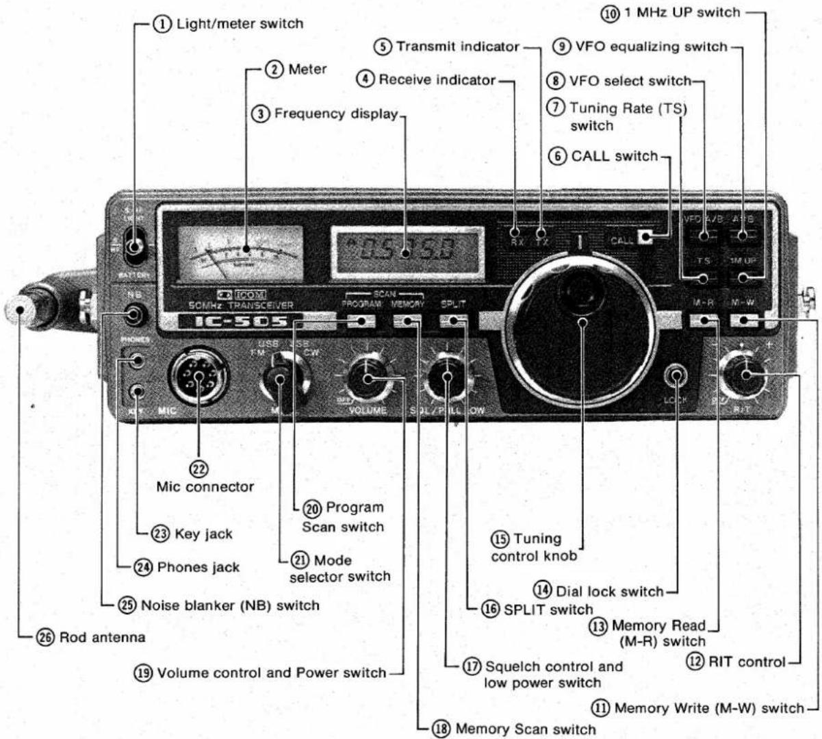
1. Light/Meter switch:
When switch lever is in upper (LIGHT) position the meter functions as an S-meter in receive mode and a relative RF output meter in transmit mode, and the meter and frequency display light up. When using battery to power the IC-505, keep switch lever at center (S/RF) position to save power. At this time, the meter functions as S/RF meter and illumination is turned off. When switch lever is in lower position (BATTERY) illumination lamp turns on and meter functions to check battery voltage.
NOTE: If battery check is done with squelch closed it may temporarily open up.
2. Meter:
Shows signal strength on the S scale in receive mode, relative power output on the RF in transmit mode, and battery voltage at the bottom.
Replace cells if meter pointer moves out of red zone during transmission.
3. Frequency display:
Indicates operating frequency, VFO in use, selected memory channel, CALL channel, and Split and Scan operation modes.
The tilted LCD polarizing panel provides easy reading of display information.
- Receive indicator:
The LED glows when squelch is opened in receive mode.
- Transmit indicator:
The LED lights when PTT switch on the microphone is pressed during SSB or FM (optional) mode. This indicates that IC-505 is in transmit mode.
In CW mode. the LED lights when the CW break-in circuit is activated by keying.
- CALL switch:
Press this switch to "read" the frequency stored in CALL channel. The frequency data in CALL channel can be re-written in the same manner as in other memory channels.
- Tuning Rate (TS) switch:
This switch sets tuning rate to 1 kHz regardless of operating mode.
- VFO select switch:
Selects either A or B VFO frequencies.
- VFO equalizing (A=B) switch:
Press this switch to transfer A or B VFO's frequency to the other VFO. Also this can be used to reset scan stop timer.
Press this switch while the scan is stopping on a frequency.
- 1 MHz UP (1M UP) switch:
Each push increases the operating frequency in 1 MHz steps. The lower digits remain the same. When the frequency is in the 53 MHz range, by pressing this switch, the frequency will change to the 50 MHz range.
- Memory Write (M-W) switch:
Allows you to store any desired frequency into either Memory or CALL channel.
- RIT control:
Offsets the receiving frequency ±1 kHz either side of the transmitting frequency without changing transmitting frequency. If the RIT control is at the OFF position or at the top (12 o'clock) position, both transmitting and receiving frequencies are the same.
Rotate RIT control clockwise to increase receiving frequency, and counterclockwise to decrease the receiving frequency.
- Memory Read (M-R) switch:
Press this switch to select the frequency stored in one of the six memory channels (M1-M6). Each push selects a memory channel having the next higher number. (When the operating channel is M6, the next push selects M1.)
- Dial Lock switch:
Electrically locks the operating frequency. This eliminates dial rotation by misoperation during long QSO or portable operation.
- Tuning Control knob:
Tunes the transmitting/receiving frequency. Rotate clockwise to increase the frequency, and counterclockwise to decrease the frequency. The tuning rate is 100 Hz for SSB or CW, 10 kHz for FM, and 1 kHz for all modes when TS switch is turned on.
When this control knob rotated clockwise beyond the upper limit frequency, the lower limit frequency will be selected. When the control is rotated counterclockwise below the lower limit, the upper limit frequency will be selected.
16. SPLIT switch:
Selects the relationship of the two VFO's. In the out position, one VFO is for both transmit and receive. In the SPLIT (in) position, the VFO selected by the VFO select switch is for receive and the other is for transmit.
17. Squelch control and low power switch:
Turning this control clockwise sets the squelch threshold higher. To turn OFF the squelch function, turn this control completely counterclockwise. As squelch circuit performs Auto Stop detection during scanning, this control should be at a position where no noise is heard during scanning.
By pulling the squelch control knob, the RF output power is reduced to 0.5 watts when the power amp switch is in the 3W position. These functions activate in any mode.
18. Memory Scan switch:
Activates Memory Scan function to search memory channels M1 to M6 in sequence.
19. Volume control and Power switch:
When the control is turned completely counterclockwise, the power is OFF. By turning the control clockwise beyond the "click", the unit is turned ON and the audio level increases by further rotating it clockwise.
20. Program Scan switch:
Activates Program Scan function to continuously search the range of frequencies stored in M1 and M2 at their corresponding scanning rate.
21. Mode select switch:
Selects any desired operation mode.
NOTE: Although the SSB has both USB and LSB, USB is more commonly used on the 50 MHz band.
FM operating requires an optional FM unit.
22. Mic connector:
Connect the supplied microphone to this jack. Optional Desk Microphone (IC-SM5) and Up/Down Microphone (IC-HM11) can also be connected.
NOTE: Only a microphone with a built-in preamp can be used with this mic connector.
23. Key jack:
Connect key in CW mode. Use the supplied key plug.
24. Phones jack:
Connect an accessory earphone or an external speaker. Use supplied speaker plug.
25. Noise blanker (NB) switch:
In receive mode, turn on NB switch to cut pulse-type noise such as automobile ignition noise. Note that the noise blanker circuit operates only in SSB and CW modes.
26. Rod antenna:
Fully extend the 1.5 m antenna when using it in operating the IC-505. When using an external antenna, fully retract rod antenna.
CAUTION: Use an antenna matched in impedance with the IC-505 when operating it in 10 watt output mode.
REAR PANEL
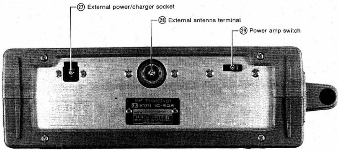
27. External power/charger socket:
Connect a power supply having regulated 13.8V DC and capable of 3A or more for 10W transmission. A DC power cable is included in accessory kit. The transceiver socket is also used to recharge the rechargeable Nickel-Cadmium battery pack (IC-BP10 optional). See battery pack manual for directions.
28. External antenna terminal:
Connect any antenna having 50-ohm impedance. Use a PL-259 connector.
29. Power amp switch:
Turns power amp on and off to step up output power. When the squelch/low power switch is in the normal position, turn this switch on to increase power output from 3W to 10W.
NOTE: When using the IC-505 with batteries, keep this switch in the OFF (3W) position, because its current drain is too much and the battery life may be very short.
CAUTION: In 10W output mode, use matched external antenna; if built-in rod antenna is used, unstable operation may occur, and cause interference to other stations.
USE SPECIFIED POWER SOURCE
Please use either size-C dry cells (nine cells), Nickel-Cadmium battery pack (IC-BP10), or external power supply with 13.8V DC such as a car battery or regulated power supply.
Load nine cells in the pack.
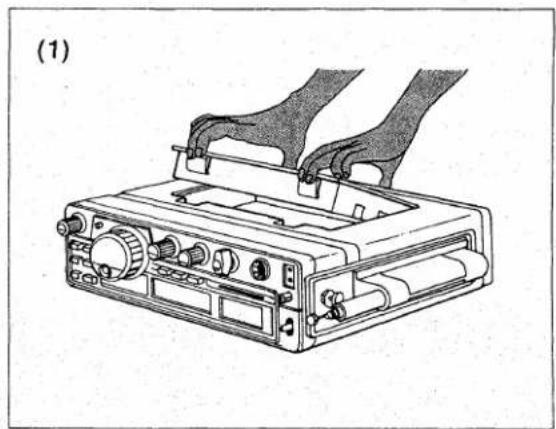
Follow procedure below to load cells into battery pack. Nine size-C cells are included in the accessory kit.
1. How to load cells:
(1) Remove battery pack from transceiver.
(2) Slide the cover open. (When cover is opened approx. 1/3 of its length, it locks, and prevents sliding).
(3) Place the nine cells in correct position according to indicated polarity.
(4) Close cover and place the battery pack in position.
natural_image
Technical line drawing of a portable electronic device with two hands operating it (no text or symbols visible)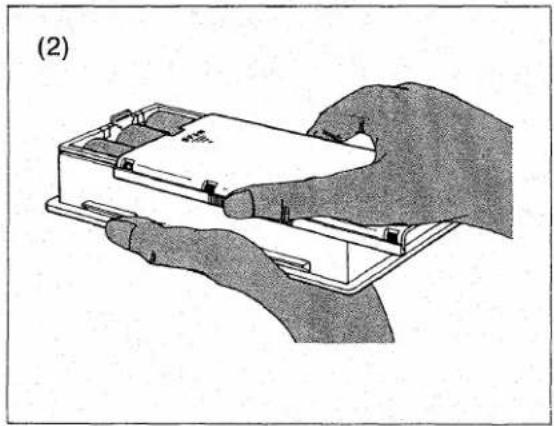
natural_image
Illustration of two hands assembling a device with a paper inside (no text or symbols visible)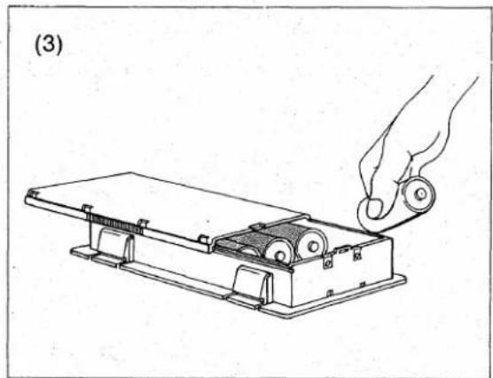
natural_image
Line drawing of a hand inserting rollers into a device (no text or symbols)2. Battery replacement interval:
Check voltage level with Light/Meter switch, and replace cells if meter reading falls below the red zone. If meter reading drops excessively in the transmit mode, replace cells.
NOTE: Replace all nine cells at one time. Also, do not intermix new and old cells, or battery life may be shortened or other problems may occur. If the IC-505 will not be used for long periods of time, remove the cells to prevent leakage.
Nickel-Cadmium rechargeable battery pack IC-BP10 (optional)
The IC-BP10 has ten N-900C Nickel-Cadmium batteries. First, recharge the battery pack, then mount it in the IC-505 using the same procedure as for the supplied battery pack. Refer to the separate Nickel-Cadmium Battery Pack Instruction Manual for detailed information.
How to extend battery life
(1) Try to keep your transmission time short.
(2) Keep sound level low during receiving.
(3) Turn the power switch off when the IC-505 is not in use.
(4) Turn illumination lamp on only when needed.
(5) Avoid using the IC-505 over long periods of time.
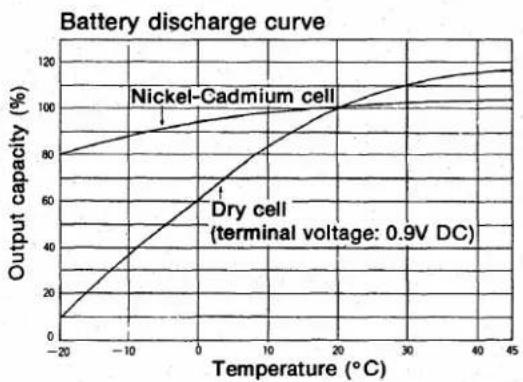
(6) Keep batteries warm when using IC-505 in a cold environment. (When temperature drops, battery capacity, will drop.)
Battery discharge curve
Typical battery capacity reduction in ambient temperatures is given in the diagram below. This data shows that dry cell batteries must be kept warm under cold conditions. We recommend using the Nickel-Cadmium battery as it has higher stability against low temperatures.
Battery capacity reduction ratio against ambient temperatures
line
| Temperature (°C) | Nickel-Cadmium cell Output capacity (%) | Dry cell (terminal voltage: 0.9V DC) Output capacity (%) | | ---------------- | ---------------------------------------- | ------------------------------------------------------ | | -20 | 80 | 0 | | 0 | 90 | 60 | | 20 | 100 | 100 | | 40 | 115 | 115 | | 45 | 120 | 120 |Battery life and output power chart
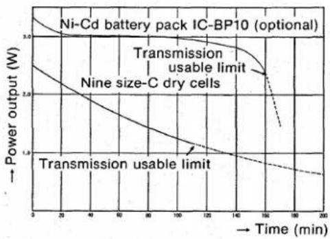
Testing conditions:
• Mode: CW • Ambient temperature: 25°C
• Repeated 3-min receiving and 1-min transmitting
line
| Time (min) | Ni-Cd battery pack IC-BP10 (optional) Power output (W) | Nine size-C dry cells Power output (W) | | ---------- | ---------------------------------------------------- | -------------------------------------- | | 0 | 3.0 | 2.5 | | 40 | ~2.8 | ~2.2 | | 80 | ~2.6 | ~2.0 | | 120 | ~2.4 | ~1.8 | | 160 | ~2.2 | ~1.7 | | 200 | ~2.0 | ~1.6 |AC power supply
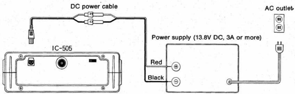
For fixed station operation, use an AC power supply which provides 13.8V DC and capable of 3A or more.
A wiring guide is given below.
Connecting power supply
NOTE: If any frequency is set in any one mode, that frequency is stored in the memory. Thus, frequency will not vary when mode switch is changed (except when the tuning control knob is turned, in which case the above example does not apply), and the stored frequency will be displayed when the mode switch is returned to the previous mode.
MEMORY CHANNELS
The IC-505 transceiver has six memory channels (M1-M6) and a CALL channel, in which you can "re-write" the stored memory frequency.
How to Memorize the Desired Frequency
NOTE: Only frequencies set by VFO A and VFO B can be stored in these memory channels and CALL channel.
(1) Select any desired frequency by using either VFO A or VFO B.
(2) Press M-R switch "n" times to select "n-th" memory channel (from M1 to M6). When you wish to store the frequency in the CALL channel, press CALL switch instead. The frequency previously stored will appear on the display panel.
(3) Press M-W switch. The new frequency is now in the "n-th" memory (or in CALL channel) and is displayed on the frequency display.
| Operation on front panel | Frequency on the display. |
(1) Select any desired frequency using the tuning control knob.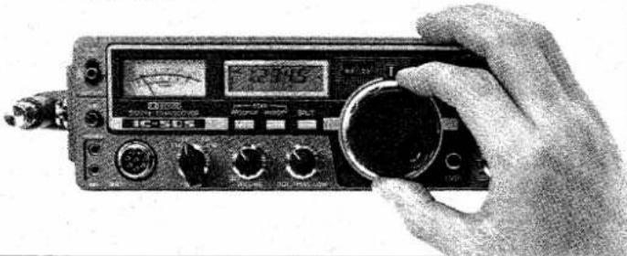 | If you select, for instance, 51.234.5 MHz with VFO A, the display shows: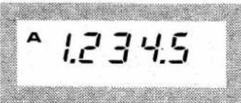 |
(2) Press the M-R switch three times in succession to select the M3 memory. (You can store the frequency in memory M3.)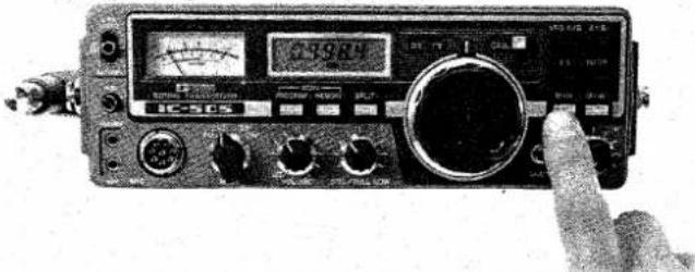 | At this time, “M3” and the frequency which was stored before will appear on the display.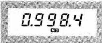 |
(3) Press the M-W switch.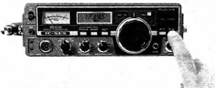 | 51.234.5 MHz has been stored in memory M3 and is shown on the display.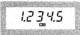 |
How to Call Frequency from Memory
Press either the M-R switch or CALL switch to call and display the stored frequency.
Memory Back-Up Cells
In general computer construction, data can be held in memory only when electric power is continuously applied. In other words, battery power is required to keep contents in memory. The IC-505 uses four AA cells for memory back-up.
Since memory back-up takes very little current, these cells can usually be used for more than a year.
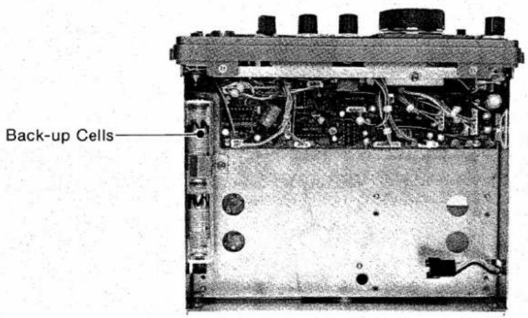
CAUTION: Replace these AA cells once a year. Replace the cells WITHIN FIVE MINUTES, since the capacitor can hold only a charge sufficient to power memory for approximately five minutes.
SCANNING
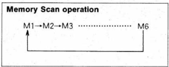
The IC-505 has two frequency scanning functions: the Memory Scan which repeatedly searches six memory channels, and the Program Scan which repeats scanning between frequencies stored in memories M1 and M2.
Memory Scan
Continuous scanning of memory channels M1 to M6.
flowchart
graph TD
    A["M1"] --> B["M2"]
    B --> C["M3"]
    C --> D["......"]
    D --> E["M6"]
1. How to perform Memory Scan
(1) Store any desired frequencies into six memory channels (M1-M6).
(2) Press the MEMORY SCAN switch. Memory scan operation will start. Press the CALL switch, if you wish to include the CALL channel in the scanning loop.
2. How to stop Memory Scan
(1) Auto stop by squelch function:
If the squelch control is rotated clockwise to cut noise before memory scan starts, scanning will automatically stop on a memory channel in which a signal has been received (the squelch has been opened).
When scanning stops, the timer starts. After 15 seconds, scanning will restart. Press the MEMORY SCAN switch again or press the PROGRAM SCAN to stop scanning.
(2) Stop scanning by use of the MEMORY SCAN switch:
To stop scanning, simply press the MEMORY SCAN (or PROGRAM SCAN) switch during scan operation.
Note: The frequency of the memory channel where scanning stops will be written into VFO A or VFO B, depending on the VFO select switch position.
3. To restart Memory Scan operation, press the MEMORY SCAN switch again.
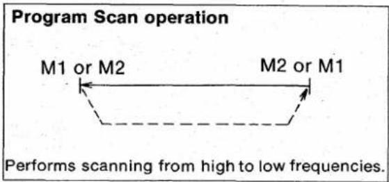
Program Scan
Continuous scanning between frequencies stored in memory channels M1 and M2.
The scan rate is determined by operating mode and TS switch position (100 Hz in SSB and CW modes, 10 kHz in FM mode, and 1 kHz in any mode when the TS switch is pushed).
1. How to perform Program Scan
(1) Store upper and lower limit frequencies into memory channels M1 and M2.
(2) Press the PROGRAM SCAN switch and its operation will start. Note: Scanning is done from high frequency to low frequency. If the same frequency is stored in M1 and M2, the SCAN indicator on the frequency display flashes but the frequency will not be changed.
2. How to Stop Program Scan
(1) Auto stop squelch circuit:
If the squelch control is rotated clockwise to cut the noise before program scan starts, scanning will automatically stop at a frequency which has received a signal.
When scanning stops, the timer starts. After 15 seconds, scanning will restart. Press the PROGRAM SCAN switch or MEMORY SCAN switch to stop scanning.
(2) To stop scanning by PROGRAM SCAN switch:
To stop scanning, press the PROGRAM SCAN (or MEMORY SCAN) switch during scan operation.
NOTE: The frequency that the scan has been stopped at will be written into VFO A or VFO B, depending on the VFO select switch position.
If the low end frequency of the band (0.000.0) is stored into M1 or M2 as a lower limit frequency, you can scan the entire band regardless of the frequency in the other memory channel.
3. Restart Program Scan
To restart Program Scan, press the PROGRAM SCAN switch again. Program scanning will start at the upper limit frequency.
How to Reset the Timer
When either Program or Memory Scan operation stops, the timer starts counting. To reset the timer, press the VFO equalizing switch. The scan operation will start again from the frequency which the scan has been stopped at.
PRE-OPERATION CHECK
Before you turn on the power switch, check the following:
- Check to be sure that all cells and battery pack are in position with proper polarity. If an external power supply is used, check for correct cabling.
- Fully extend the rod antenna. If an external antenna is connected, fully retract the rod antenna. Check antenna connection.
- Make sure the microphone or key is properly connected.
SSB OPERATION
The SSB has both USB and LSB; USB is used more commonly for 50 MHz band operation.
SSB Receiving
- Before turning the power switch on, set each switch and control as follows:
| MODE switch | USB |
| VOLUME controland POWER switch | OFF (fully counterclockwise) |
| SQUELCH controland LOW POWER switch | Fully counterclockwise (Pushed in is normal position.) |
| LOCK switch | OFF (out) |
| RIT control | Center (12 o'clock) position (or RIT switch OFF) |
| TS switch | OFF (out) |
| LIGHT/METER switch | S/RF (center position) |
- Rotate the VOLUME control clockwise. The power will be applied and the operation frequency will appear on the frequency display.
- Rotate the VOLUME control clockwise to an appropriate sound level.
- Rotate the tuning control knob to increase (clockwise) or decrease (counterclockwise) the frequency.
NOTE: When the highest frequency (53.999.9 MHz, or 53.9984 MHz in USB mode) is selected, rotating the tuning control clockwise will select the lowest frequency (50.000.0 MHz, or 49.9986 MHz in USB). Rotating the tuning control counterclockwise beyond the lowest frequency will select the highest-frequency.
The tuning rate in each mode is as follows:
| Mode | Frequency step | Per single knob rotation |
| FM | 10 kHz | 500 kHz |
| USBLSBCW | 100 Hz | 5 kHz |
| TS ON | 1 kHz | 50 kHz |
- Since the SSB signal has no carrier, no beat tone can be heard even when the signal is received. Set the tuning control in position where the S meter has the highest indication level so that the voice can normally be heard. An accurate 100 Hz step tuning rate permits quick and easy tuning.
SSB Transmission
NOTE: Before transmitting, listen in the receive mode to make sure your transmission will not interfere with other communications.
-
Press the PTT switch of the microphone. The transmit indicator will light up.
-
Speak while checking the meter reading.
Note: SSB waveforms vary in their amplitude depending on voice level. However, an excessively loud voice cannot increase output level beyond its limit, and may cause spurious radiation. Also, your voice may be distorted.
CW OPERATION
Set the MODE switch to CW. Set the other switches and controls in the same manner as for SSB operation.
CW receiving
The transmit frequency will be the same as the received signal's frequency when it makes an approximately 800 Hz beat tone. Perform tuning by referring to CW monitor tone (approximately 800 Hz).
CW transmission
- Use supplied key plug, and connect key to the KEY jack on the front panel.
NOTE: When connecting an electric keyer, observe the proper polarity. If the semiconductor switching circuit is used, set the + line voltage to less than 0.4 volts in key down condition.
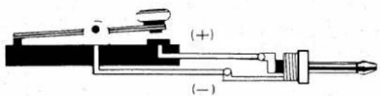
- When keying, the unit is automatically set in the transmit mode. After keying, it is returned to the receive mode, also automatically, after a given transmit-release delay time constant. When you key the keyer, the transmit indicator is lit and the meter needle moves and your CW signal is transmitted.
SECTION VI CIRCUIT OPERATION
The IC-505 transceiver, designed to be used for 50 MHz SSB, CW, and optional FM applications, employs a circuit with a 13.99 MHz first IF of single conversion superheterodyne (and double conversion superheterodyne with 455 kHz second IF for FM). It basically consists of five units: MAIN (A), MAIN (B), PLL, LOGIC, and front-panel EF units. These units are discussed in detail in the following sections.
1. MAIN (A) Unit
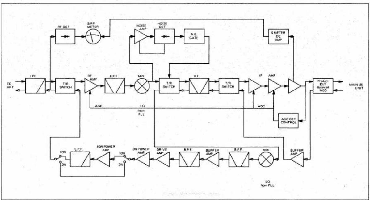
Consists of the antenna switching circuit and receiving circuitries, such as RF amplifier, IF amplifier, and product detector circuits, as well as transmitting circuits such as balanced modulator, IF amplifier, and power amplifier circuits.
An incoming signal from the antenna is fed to the antenna switching circuit through the low-pass filter, then to the RF amplifier which is a dual-gate MOS FET (3SK74) featuring a low noise figure.
The amplified signal from the RF amplifier is then sent via the band-pass filter to the mixer circuit, with a local oscillator frequency signal from the PLL circuit, and they are mixed to get a 13.99 MHz first IF signal. Note that the tracking control signal from the PLL unit is always applied to tune the band-pass filter for operating frequency.
The 13.99 MHz first IF signal is then sent to the small-size, high-performance crystal filter to provide the required pass-band response for SSB operation. It is then sent to and amplified at dual-gate MOS FET's (3SK74's) and IC BA401. Here, the signal is amplified to the appropriate level before being sent to the product detector IC ( PC1037H) at the next stage. At the product detector, the input signal and the signal from BFO circuit are mixed and converted into an AF signal, which is sent to the AF amplifier circuit of the MAIN (B) unit.
A part of the signal of IF amplifier is passed through the AGC detector and is further applied as an AGC voltage to both the RF and IF amplifier circuits. Similarly, a partial signal from the mixer circuit is passed through noise amplifier and noise detector circuits, and is used to control the noise gate (Noise Blanker) circuit. This prevents the noise signal from going to the next stage (especially when the noise blanket is on).
In the transmit mode, a voice signal being amplified by the mic amplifier circuit of the MAIN (B) unit is applied to the balanced-modulator IC ( PC1037H), which is also used as the product detector in the receive mode. This IC mixes BFO signals and AF signals to generate DSB signals. The DSB signal is further buffered, amplified, and is passed through the crystal filter (which is also used in the receive mode) where it is converted into a 13.99 MHz SSB signal.
flowchart
graph TD
    A["TO ANT"] --> B["LFF"]
    B --> C["T/R SWITCH"]
    C --> D["RF AMP"]
    D --> E["B.P.F."]
    E --> F["MIX"]
    F --> G["T/R SWITCH"]
    G --> H["X.F."]
    H --> I["T/R SWITCH"]
    I --> J["IF AMP"]
    J --> K["Product DDT Balanced MOD"]
    K --> L["MAIN (B) UNIT"]
    M["AGC"] --> N["10W 3W"]
    N --> O["L.P.F."]
    O --> P["10W POWER AMP"]
    P --> Q["3W POWER AMP"]
    Q --> R["DRIVE AMP"]
    R --> S["B.P.F."]
    S --> T["BUFFER AMP"]
    T --> U["B.P.F."]
    U --> V["MIX"]
    V --> W["BUFFER AMP"]
    W --> X["AGC DET CONTROL"]
    X --> Y["5 METER DC AMP"]
    Y --> Z["NOISE DET"]
    Z --> AA["RF DET"]
    AA --> AB["S/RF METER"]
    AB --> AC["LO from PLL"]
    AC --> AD["AND Gate"]
    AD --> AE["N.B."]
    AE --> AF["NOISE AMP"]
    AF --> AG["RF DET"]
    AG --> AH["S/RF METER"]
    AH --> AI["LO from PLL"]
At the double-balanced MIXER IC (SN76514), the 13.99 MHz SSB signal is mixed with the local oscillator signal coming from the PLL unit, thus generating a 50 MHz SSB signal. This signal then passes through the band-pass filter, then buffer amplifier Q20, and again the band-pass filter. Further, the signal goes to the driver amplifier and power amplifier, where it is amplified to either 3W or 10W power output. Note that two band-pass filters located before and after the buffer amplifier, always receive tracking control voltages from PLL unit in the same manner as in the receive mode. Thus, the filters are tuned to the transmitting frequency.
The amplified 3W (or 10W) signal is then sent via the antenna switching circuit to the built-in rod antenna or an external antenna terminal.
2. MAIN (B) Unit
Consists of an AF amplifier and squelch circuits for reception, and a mic amplifier, CW monitor, and APC circuits for transmission, as well as the regulated power supply circuit. In the receive mode, the signal coming from the product detector of the MAIN (A) unit is applied to the AF amplifier IC ( PC575C2) to drive the speaker.
In the transmission mode, the audio signal from the microphone is fed into the audio-frequency amplifier IC ( PC566H) where the signal is amplified before being sent to the balanced-modulator circuit.
During CW operation, the key grounds the emitter of oscillator transistor, thus generating an approximately 800 Hz CW side-tone signal. This signal is applied to the AF amplifier circuit which drives the speaker.
Here, 50 MHz output power is controlled by an APC circuit to reduce driving power at buffer stage when an overcurrent flows through the 10W power amplifier transistor.
3. PLL Unit
Consists of the mixed down PLL (Phase-Locked Loop) circuit which is logically controlled by the microprocessor (CPU) of the LOGIC unit. The PLL unit generates a local oscillator frequency to be applied to the transmitting/receiving mixer circuit of the MAIN (A) unit. The local oscillator circuit of this unit generates a 19.64 MHz signal. It is then multiplied three times, and is sent to the PLL mixer circuit. Here, the local oscillator circuit has the VXO (Variable Xtal Oscillator) configuration and generates an 100 Hz-step frequency using a D/A (Digital/Analog) converted voltage sent from the LOGIC unit.
In the PLL loop, the reference crystal oscillator signal of 5.12 MHz is divided by 512 and thus a 10 kHz signal is generated. This signal permits a 10 kHz step signal in the range of 63.99 MHz to 67.98 MHz as the local oscillator frequency.
Moreover, the PLL unit sends a tracking control signal to the band-pass filters of the MAIN (A) unit.
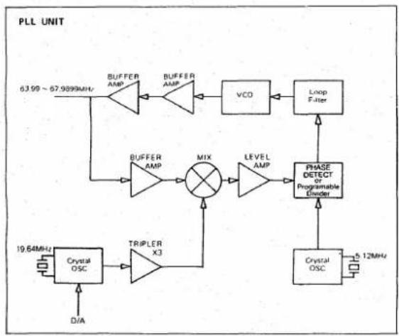
flowchart
graph TD
    A["63.99 ~ 67.9899MHz"] --> B["BUFFER AMP"]
    B --> C["BUFFER AMP"]
    C --> D["VCD"]
    D --> E["Loop Filter"]
    E --> F["MIX"]
    F --> G["LEVEL AMP"]
    G --> H["PHASE DETECT or Programmable Divider"]
    H --> I["Crystal OSC"]
    I --> J["TRIPLER X3"]
    J --> K["19.64MHz Crystal OSC"]
    K --> L["D/A"]
    M["19.64MHz Crystal OSC"] --> N["TRIPLER X3"]
    N --> O["19.64MHz D/A"]
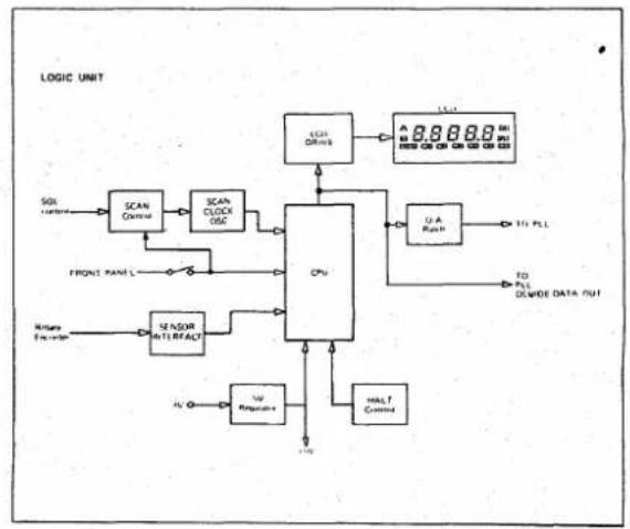
flowchart
graph TD
    A["LOGIC UNIT"] --> B["CPU"]
    B --> C["ADC/Offload"]
    B --> D["U-A/Match"]
    B --> E["MOLT Control"]
    B --> F["SWI Response"]
    B --> G["FRONT PANEL"]
    B --> H["SCAN/Control"]
    B --> I["SCAN/CLOCK/OSC"]
    B --> J["SOI Control"]
    B --> K["SOI Response"]
    B --> L["SOI Response"]
    B --> M["SOI Response"]
    B --> N["SOI Response"]
    B --> O["SOI Response"]
    B --> P["SOI Response"]
    B --> Q["SOI Response"]
    B --> R["SOI Response"]
    B --> S["SOI Response"]
    B --> T["SOI Response"]
    B --> U["SOI Response"]
    B --> V["SOI Response"]
    B --> W["SOI Response"]
    B --> X["SOI Response"]
    B --> Y["SOI Response"]
    B --> Z["SOI Response"]
    B --> AA["SOI Response"]
    B --> AB["SOI Response"]
    B --> AC["SOI Response"]
    B --> AD["SOI Response"]
    B --> AE["SOI Response"]
    B --> AF["SOI Response"]
    B --> AG["SOI Response"]
    B --> AH["SOI Response"]
    B --> AI["SOI Response"]
    B --> AJ["SOI Response"]
    B --> AK["SOI Response"]
    B --> AL["SOI Response"]
    B --> AM["SOI Response"]
    B --> AN["SOI Response"]
    B --> AO["SOI Response"]
    B --> AP["SOI Response"]
    B --> AQ["SOI Response"]
    B --> AR["SOI Response"]
    B --> AS["SOI Response"]
    B --> AT["SOI Response"]
    B --> AU["SOI Response"]
    B --> AV["SOI Response"]
    B --> AW["SOI Response"]
    B --> AX["SOI Response"]
    B --> AY["SOI Response"]
    B --> AZ["SOI Response"]
    B --> BA["SOI Response"]
    B --> BB["SOI Response"]
    B --> BC["SOI Response"]
    B --> BD["SOI Response"]
    B --> BE["SOI Response"]
    B --> BF["SOI Response"]
    B --> BG["SOI Response"]
    B --> BH["SOI Response"]
    B --> BI["SOI Response"]
    B --> BJ["SOI Response"]
    B --> BK["SOI Response"]
    B --> BL["SOI Response"]
    B --> BM["SOI Response"]
    B --> BN["SOI Response"]
    B --> BO["SOI Response"]
    B --> BP["SOI Response"]
    B --> BQ["SOI Response"]
    B --> BR["SOI Response"]
    B --> BS["SOI Response"]
    B --> BT["SOI Response"]
    B --> BU["SOI Response"]
    B --> BV["SOI Response"]
    B --> BW["SOI Response"]
    B --> BX["SOI Response"]
    B --> BY["SOI Response"]
    B --> BZ["SOI Response"]
    B --> CA["SOI Response"]
    B --> CB["SOI Response"]
    B --> CC["SOI Response"]
    B --> CD["SOI Response"]
    B --> CE["SOI Response"]
    B --> CF["SOI Response"]
    B --> CG["SOI Response"]
    B --> CH["SOI Response"]
    B --> CI["SOI Response"]
    B --> CJ["SOI Response"]
    B --> CK["SOI Response"]
4. LOGIC Unit
Consists of the C-MOS 4-bit microcomputer (CPU) where all the necessary operation programs are in the ROM, input matrix circuit, HALT circuit, and D/A latch circuit.
When rotating the tuning control knob, pulses are generated and are read sequentially into the CPU via the sensor interface circuit. The resultant data, which meets the specification of input matrix, is sent to both display circuit and PLL unit. Note: Selecting functions such as Scan function and VFO switching is performed by the input matrix circuit.
5. EF Unit at Front Panel
This unit is located on the front panel and has a variety of functional switches, controls, sensors directly coupled to tuning control knob, liquid-crystal display (LCD) panel, and LCD driver circuit.
Any display data given by the CPU of the LOGIC unit is sent to the LCD driver IC (TP041) which can directly drive the liquid-crystal display panel.
SECTION VII PRECAUTIONS
BASIC PRECAUTIONS
To operate the IC-505 transceiver at optimum performance, the following basic precautions should always be followed:
(1) Use only the specified battery packs or a power supply having regulated 13.8V DC and capable of 3A or more.
(2) Do not open the factory-assembled and fine-tuned transceiver set. Also, never turn the cores and trimmers in their adjusted positions.
(3) When operating a transceiver, you should have a license and must follow the applicable regulations.
(4) When using the IC-505 in a cold place, we recommend warming the battery pack to provide sufficient battery power (see section on Battery Discharge Curve on page 8).
(5) The IC-505 is rigid enough for normal operations, but its construction is not waterproof. Keep the transceiver protected from water.
DAILY CARE AND MAINTENANCE
(1) Clean transceiver with a dry, soft cloth. Do not use any organic solvent such as lacquer thinner, or the finish coating may be damaged.
(2) When using the transceiver with dry cells or Nickel-Cadmium cells, check them for leakage at regular intervals.
(3) If any problem occurs during normal operation, bring or send the transceiver to your dealer or directly to an ICOM service center.
SECTION VIII BASIC PARTS LAYOUT
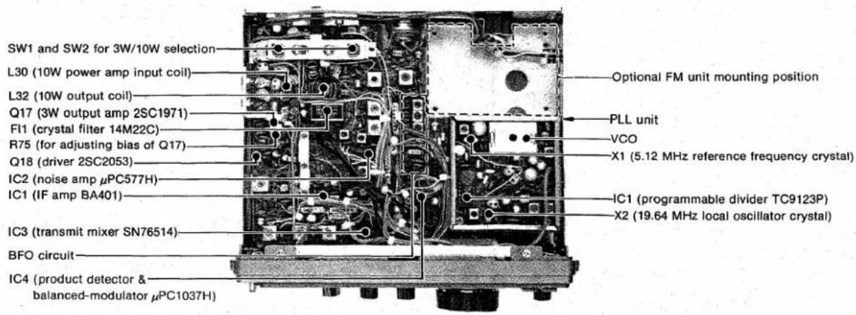
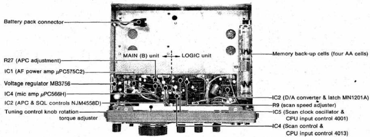
SECTION IX TROUBLESHOOTING GUIDE
Follow instructions given in the troubleshooting table. However, if any problem cannot be corrected, call your dealer or ICOM service center.
| Problem | Cause(s) | Solution |
| Power failure | Battery pack in poor contact with transceiver.Battery has been exhausted.Cells are not in correct polarity.Poor contact to external power supply. | Clean contact points (electrodes).Replace with new cells or recharge Ni-Cd cells.Check for correct battery polarity.Check power connection. |
| No sound from speaker | Volume control is fully counterclockwise.Squelch circuit is on.An external speaker or headphone is connected.In transmit mode.Battery voltage is low. | Rotate VOLUME control clockwise.Rotate squelch control counterclockwise.Check for open audio circuit.Select Receive mode.Replace or recharge cells. |
| Poor sensitivity | Rod antenna is not extended enough.Incorrect external antenna is used or antenna circuit is open or shorted. | Fully extend rod antenna.Check coaxial cable and external antenna for proper connection. |
| No or low RF output | Defective PTT switchIn Low Power mode. | Check PTT switch on the microphone.Power amp is off and/or LOW power switch is in LOW position. |
| No modulation | Mic connector is in poor contact.Mic plug or its related circuit is open. | Check mic connector.Check wiring at mic plug. |
| The set works normally but cannot make a contact. | RIT is on, thus receiving and transmitting frequencies are not the same.SPLIT switch is on, thus receiving and transmitting frequencies are not the same. | Turn RIT off or set it in 12 o'clock position.Turn off SPLIT switch by pressing it again. |
| No frequency can be written into memory. | Frequency was set other than in VFO. | Set frequency again with VFO A or VFO B. |
| Frequency data in memory has disappeared. | Back-up cells have been exhausted. | Replace back-up cells. |
| Memory Scan does not work. | The same frequency was set in memory channels. | Enter different frequencies into memory channels. |
| Program Scan does not work. | The same frequency was set in M1 and M2. | Enter different frequencies into M1 and M2. |
| The scan does not stop even if a signal is received. | Squelch does not operate. | Rotate squelch control clockwise until noise stops. |
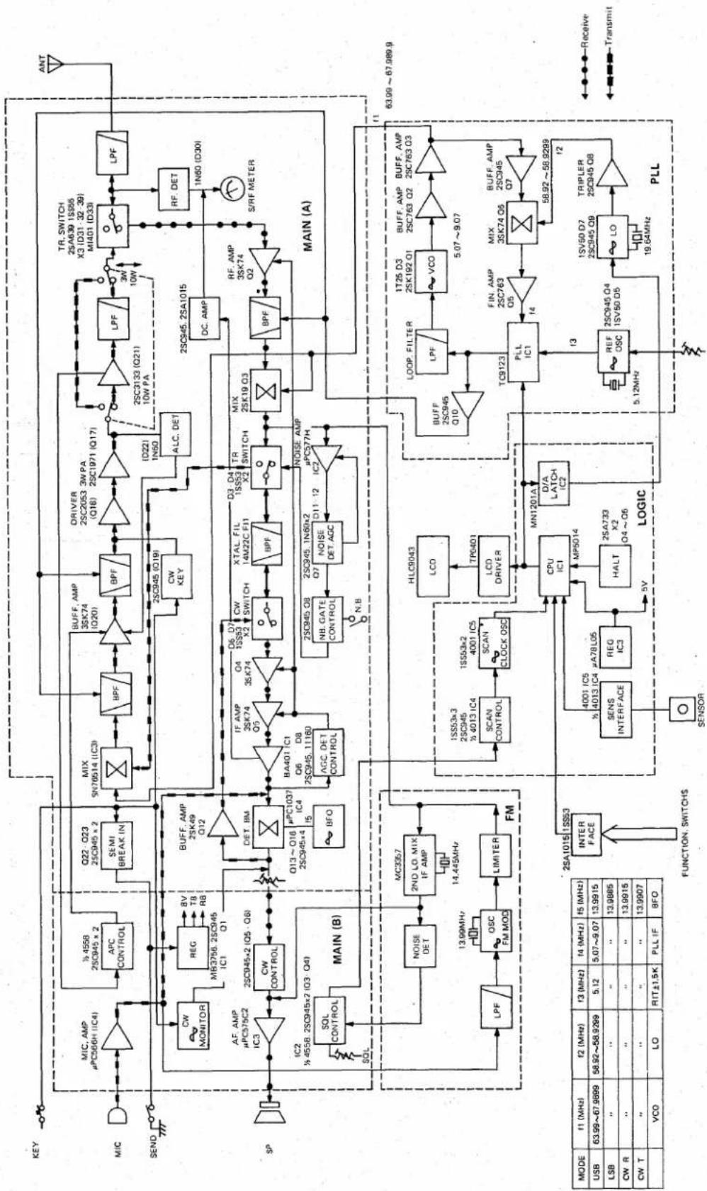
flowchart
graph TD
    subgraph Inputs
        direction TB
        KEY --> MIC
        MIC -->|MIX, 4558/2SC945×2| APC
        APC -->|SEM1 BREAK IN| MIX
        MIX --> BPF
        BPF --> BPF
        BPF --> 2SC945(019)
        2SC945(019) -->|AIF AMP 2SK49 Q12| DET_BM
        DET_BM -->|CW MONITOR| REG
        REG -->|MB3756.2SC945 IC1 Q1| ACFAMP
        ACFAMP -->|AW 4558.2SC945×2 IC3 Q6| CW
        CW -->|IC3| SQ
        SQ -->|SQL CONTROL| SQL
        SQL -->|SQL| WM
        WM -->|NOISE DET| NOISE_DET
        NOISE_DET --> MC3357["2ND LO. MIX IF AMP"]
        MC3357 -->|13.99MHz| OSC
        OSC --> FMOD["OSC FM MOD"]
        FMOD --> LIMITER["LIMITER"]
        LIMITER --> FM
    end

    subgraph Outputs
        direction TB
        ANT --> LPF
        Ant --> RF_DET
        RF_DET --> 1N60(D30)
        1N60(D30) --> S/RF_METER["S/RF METER"]
        S/RF_METER --> MAIN(A)
        MAIN(A) --> RF_AMP_3SK74_Q2
        MAIN(A) --> BPF
        BPF --> 2SC945_2SA1015["DC. AMP"]
        BPF --> 2SC945_2SA1015
        2SC945_2SA1015 --> TR_SWITCH["TR. SWITCH 2SA639 1SS55 X3 (D31:32:39)"]
        2SC945_2SA1015 --> MI401["MI401 (D33)"]
        2SC945_2SA1015 --> LPF
    end

    subgraph Outputs
        direction TB
        MAIN(A) --> RF_AMP_3SK74_Q2
        MAIN(A) --> BPF
        BPF --> 2SC945_2SA1015
        2SC945_2SA1015 --> DC.AMP
        DC.AMP --> RF_AMP_3SK74_Q2
        RF_AMP_3SK74_Q2 --> VCO
        VCO --> 1T25_D3["1T25 D3 2SK192 Q1"]
        VCO --> 2SC763_Q2["2SC763 Q2"]
        VCO --> 2SC763_Q3["2SC763 Q3"]
        2SC763_Q3 --> LOOP_FILTER["LOOP. FILTER"]
        LOOP_FILTER --> LPF
        LOOP_FILTER --> VCO
        VCO --> 5.07~9.07["5.07~9.07"]
        VCO --> 58.92~58.9289["58.92~58.9289"]
        58.92~58.9289 --> MUX["MUX"]
        MUX --> FIN_AMP["FIN. AMP 2SC763 Q5"]
        MUX --> BUFF_AMP["BUFF. AMP 2SC945 Q7"]
        MUX --> LO["LO"]
        LO --> TRIPLER["TRIPLER 2SC945 Q8"]
    end

    subgraph Outputs
        direction TB
        LOOP_FILTER --> CPU_IC1["CPU IC1"]
        CPU_IC1 --> MP5014["MP5014"]
        MP5014 --> HALT["HALT"]
        HALT --> LOGIC["LOGIC"]
        LOGIC --> SENSOR["SENSOR"]
        SENSOR --> INTERFACE["INTER FACE"]
        INTERFACE --> MODE_F1["F1 (MHz)"]
        INTERFACE --> MODE_F2["F2 (MHz)"]
        MODE_F1 --> USB_USB["USB: 63.99~67.9899"]
        MODE_F2 --> USB_LO["USB: 58.92~58.9299"]
        MODE_F2 --> USB_LSB["USB: ..."]
        MODE_R["SW R"] --> CW_R["SW R"]
        CW_R --> CW_T["SW T"]
        CW_T --> VCO["VCO: ..."]
        CPU_IC1 -->|4001 IC5 /4013 IC4 μA78L05| INTERFACE
        CPU_IC1 -->|CAPS OF CAN| INTERFACE
    end

    style MODE_F1 fill:#f9f,stroke:#333
    style MODE_F2 fill:#f9f,stroke:#333
    style MODE_F3 fill:#f9f,stroke:#333
    style MODE_F4 fill:#f9f,stroke:#333
    style MODE_F5 fill:#f9f,stroke:#333
    style MODE_F6 fill:#f9f,stroke:#333
    style MODE_F7 fill:#f9f,stroke:#333
    style MODE_F8 fill:#f9f,stroke:#333
    style MODE_F9 fill:#f9f,stroke:#333
    style MODE_F10 fill:#f9f,stroke:#333
    style MODE_F11 fill:#f9f,stroke:#333
    style MODE_F12 fill:#f9f,stroke:#333
    style MODE_F13 fill:#f9f,stroke:#333
    style MODE_F14 fill:#f9f,stroke:#333
    style MODE_F15 fill:#f9f,stroke:#333
    style MODE_F16 fill:#f9f,stroke:#333
    style MODE_F17 fill:#f9f,stroke:#333
    style MODE_F18 fill:#f9f,stroke:#333
    style MODE_F19 fill:#f9f,stroke:#333
    style MODE_F20 fill:#f9f,stroke:#333
    style MODE_F21 fill:#f9f,stroke:#333
    style MODE_F22 fill:#f9f,stroke:#333
    style MODE_F23 fill:#f9f,stroke:#333
    style MODE_F24 fill:#f9f,stroke:#333
    style MODE_F25 fill:#f9f,stroke:#333
    style MODE_F26 fill:#f9f,stroke:#333
    style MODE_F27 fill:#f9f,stroke:#333
    style MODE_F28 fill:#f9f,stroke:#333
    style MODE_F29 fill:#f9f,stroke:#333
    style MODE_F30 fill:#f9f,stroke:#333
    style MODE_F31 fill:#f9f,stroke:#333
    style MODE_F32 fill:#f9f,stroke:#333
    style MODE_F33 fill:#f9f,stroke:#333
    style MODE_F34 fill:#f9f,stroke:#333
    style MODE_F35 fill:#f9f,stroke:#333
    style MODE_F36 fill:#f9f,stroke:#333
    style MODE_F37 fill:#f9f,stroke:#333
    style MODE_F38 fill:#f9f,stroke:#333
    style MODE_F39 fill:#f9f,stroke:#333
    style MODE_F40 fill:#f9f,stroke:#333
ACCESSORIES
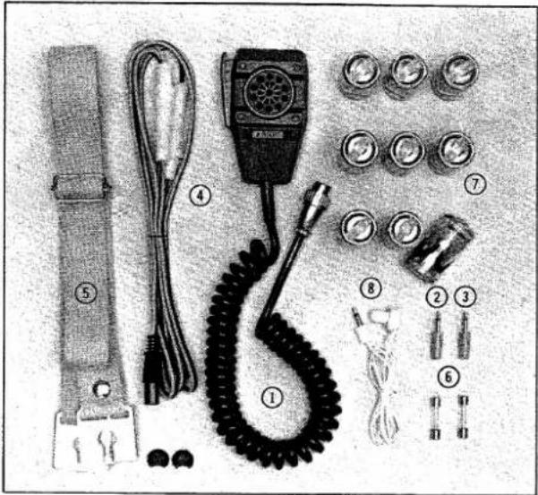
The IC-505 Accessory Kit has the following standard items:
(1) Microphone IC-HM7 1
(2) Speaker plug 1
(3) Key plug 1
(4) DC power cable 1
(5) Shoulder belt set 1
(6) 5A spare fuse....2
(7) Size-C dry cell 9
(8) Earphone.... 1
OPTIONS
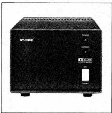
IC-3PE
AC power supply 13.8V DC, 3A
natural_image
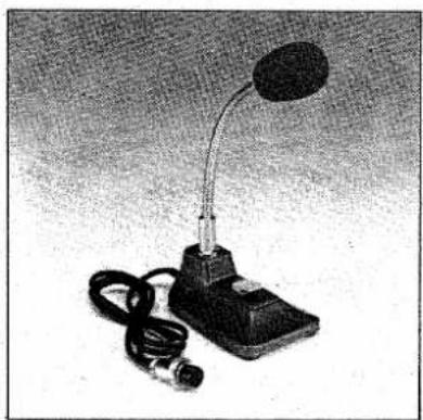
Black-and-white photo of a desktop desk lamp with adjustable arm and cord (no visible text or symbols)IC-SM5
Desk microphone
electret condenser type
natural_image
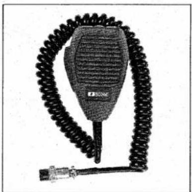
Black-and-white photo of a handheld electronic device with coiled cable and connector (no visible text or symbols)IC-HM11
Up/down microphone
| IC-BP10 | Rechargeable Nickel-Cadmium battery pack |
| IC-EX248 | FM unit |
| LC-10 | Carrying case |
| BC-15 | AC charger for battery pack IC-BP10 |

ICOM
ICOM INCORPORATED
1-6-19, KAMI KURATSUKURI, HIRANO-KU OSAKA JAPAN
- IC-505
- MHz SSB CW (FM) TRANSCEIVER
- OPERATION MANUAL
- CONTENTS
- SECTION I SPECIFICATIONS
- Versatility
- Highest receiver performance
- Distortion-free radio transmitter
- Microprocessor frequency control functions
- New liquid-crystal display panel provides clear visibility in sunlight. At night, simply turn on the switch for illumination
- Helpful accessory circuits provide quick action
- Light/Meter switch:
- Meter:
- Frequency display:
- SPLIT switch:
- Squelch control and low power switch:
- Memory Scan switch:
- Volume control and Power switch:
- Program Scan switch:
- Mode select switch:
- Mic connector:
- Key jack:
- Phones jack:
- Noise blanker (NB) switch:
- Rod antenna:
- External power/charger socket:
- External antenna terminal:
- Power amp switch:
- USE SPECIFIED POWER SOURCE
- Load nine cells in the pack.
- How to load cells:
- Battery replacement interval:
- Nickel-Cadmium rechargeable battery pack IC-BP10 (optional)
- How to extend battery life
- Battery discharge curve
- AC power supply
- MEMORY CHANNELS
- How to Memorize the Desired Frequency
- How to Call Frequency from Memory
- Memory Back-Up Cells
- SCANNING
- Memory Scan
- How to perform Memory Scan
- How to stop Memory Scan
- To restart Memory Scan operation, press the MEMORY SCAN switch again.
- Program Scan
- How to perform Program Scan
- How to Stop Program Scan
- Restart Program Scan
- How to Reset the Timer
- PRE-OPERATION CHECK
- SSB OPERATION
- SSB Receiving
- SSB Transmission
- CW OPERATION
- CW receiving
- CW transmission
- SECTION VI CIRCUIT OPERATION
- MAIN (A) Unit
- MAIN (B) Unit
- PLL Unit
- LOGIC Unit
- EF Unit at Front Panel
- SECTION VII PRECAUTIONS
- BASIC PRECAUTIONS
- DAILY CARE AND MAINTENANCE
- SECTION VIII BASIC PARTS LAYOUT
- SECTION IX TROUBLESHOOTING GUIDE
- ACCESSORIES
- The IC-505 Accessory Kit has the following standard items:
- OPTIONS
- ICOM INCORPORATED
Marke : ICOM
Modell : IC-505
Kategorie : Empfänger