
IC-502A - Empfänger ICOM - Kostenlose Bedienungsanleitung
Finden Sie kostenlos die Bedienungsanleitung des Geräts IC-502A ICOM als PDF.


| Produkttyp | Empfänger (tragbarer 6-Meter-SSB-Transceiver) |
| Marke | ICOM |
| Modell | IC-502A |
| Frequenzbereich | 50 MHz – 51 MHz |
| Frequenzstabilität | Weniger als ±200 Hz pro Stunde nach 5 Min. Einschaltzeit bei +25 °C |
| Antennenimpedanz | 50 Ω unsymmetrisch |
| Stromversorgung | DC 13,8 V ±15 % (Negative Ground), max. 800 mA |
| Stromaufnahme (Empfang) | ca. 80 mA (Ruhe), ca. 250 mA (max. Lautstärke) |
| Abmessungen (B × H × T) | 183 mm × 61 mm × 162 mm |
| Gewicht (netto) | 2,1 kg inkl. Batterien |
| Empfangssystem | Einzelfrequenz-Superhet |
| Zwischenfrequenz | 13,9985 MHz |
| Empfindlichkeit | Weniger als 0,5 μV für 10 dB S+N/N |
| Selektivität | ±1,2 kHz bei -6 dB, ±2,4 kHz bei -60 dB |
| Audio-Ausgangsleistung | Mehr als 1 W (an 8 Ω) |
| Störunterdrückung (Spurious) | Mehr als 60 dB unter Spitzenleistung |
| Betriebsarten | A3J (USB) und A1 (CW) |
| RIT (Receiver Incremental Tuning) | ±3 kHz unabhängig |
| Feinabstimmung | ±2,5 kHz |
| Rauschunterdrücker (Noise Blanker) | Ein-/Ausschaltbar |
| Stromversorgungsoptionen | 9 × C-Zellen-Batterien oder externe 13,8 V DC; NiCd-Akku BC-20/BC-15 optional |
| Zubehör im Lieferumfang | Dynamikmikrofon, Mikrofonkoffer, Schultergurt, Netzkabel, Ohrhörer, Batterietuben, Ersatzsicherung |
Häufig gestellte Fragen - IC-502A ICOM
Benutzerfragen zu IC-502A ICOM
0 Frage zu diesem Gerät. Beantworten Sie die, die Sie kennen, oder stellen Sie Ihre eigene.
Eine neue Frage zu diesem Gerät stellen
Laden Sie die Anleitung für Ihr Empfänger kostenlos im PDF-Format! Finden Sie Ihr Handbuch IC-502A - ICOM und nehmen Sie Ihr elektronisches Gerät wieder in die Hand. Auf dieser Seite sind alle Dokumente veröffentlicht, die für die Verwendung Ihres Geräts notwendig sind. IC-502A von der Marke ICOM.
BEDIENUNGSANLEITUNG IC-502A ICOM

natural_image
Close-up of a textured gray surface with a dark vertical stripe on the left side (no text or symbols)IC-502A
6 METER SSB PORTABLE TRANSCEIVER
INSTRUCTION MANUAL
TABLE OF CONTENTS
I. Specifications 1
II. Description 2
III. Accessories 3
IV. Pre-Operation 4
V. Control Functions 8
VI. Operation 11
VII. Theory of Operation 12
VIII. Maintenance and Adjustment 17
IX. Inside View 20
X. Voltage Chart 21
XI. Block Diagram 22
XII. Board Layout 23
XIII. Options 25
XIV. Schematic Diagram .... Separate
SECTION I SPECIFICATIONS
General:
| Number of Semi-conductors | Transistors 19 |
| FET 8 | |
| IC 7 | |
| Diodes 36 | |
| Frequency Coverage | 50MHz ~ 51MHz |
| Frequency Stability | Less than ±200Hz per hour after switch on 5min at +25°C |
| Antenna Impedance | 50 ohms unbalanced |
| Power Supply Requirements | DC 13.8V ± 15% Negative Ground 800mA max |
| Current Drain | Transmitting:A3J Approx. 550mA |
| A1 Approx. 750mA | |
| Receiving: At max audio approx. 250mA | |
| With no signal approx. 80mA | |
| Dial Light: Approx. 40mA | |
| Dimensions | 183mm(H) x 61mm (W) x 162mm (D) |
| Net Weight | 2.1kg including batteries |
| Transmitter: | |
| Emission Mode | A3J (USB) and A1 |
| RF Power Output | A3J 3W (PEP) |
| A1 3W | |
| Carrier Suppression | More than 40dB below peak power |
| Unwanted Sideband Suppression | More than 40dB down at 1000Hz AF input |
| Spurious Radiation | More than 60dB below peak power |
| Microphone | Impedance: 600 ohms |
| Input level: 10mV typical | |
| Dynamic or optional Electret condenser microphone | |
| CW Monitor | Built-in. Audio level adjustable by VOL knob. |
| Receiver: | |
| Receiving System | Single Conversion Superheterodyne |
| Intermediate Frequency | 13.9985MHz |
| Receiving Mode | A3J (USB) and A1 |
| Spurious Response Rejection Ratio | More than 60dB |
| Sensitivity | Less than 0.5μV for 10dB S+N/N |
| Selectivity | ±1.2KHz at -6dB |
| ±2.4KHz at -60dB | |
| Audio Output | More than 1W |
| Audio Output Impedance | 8 ohms |
Specifications subject to change without notice.
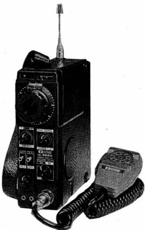
Congratulations on the purchase of the IC-502A portable 6 meter SSB transceiver. The IC-502A was designed to be operable anywhere like most portables, but we also included features found in most base sets like a very effective noise blanker, RIT, S&RF meter, CW monitor, and a full 3 watts output on USB. A highly stable VFO allows operation between 50 MHz and 51 MHz.
The aluminum die cast frame provides a very strong yet light housing for the 2 circuit boards, and the aluminum sides snap off easily if service is ever necessary or to change batteries.
natural_image
Black-and-white photo of a vintage analog oscilloscope and coiled cord device (no visible text or symbols)The IC-502A operates on 9 inexpensive C cell batteries, or an external 13.8V DC source. The IC-502A will also operate on nicad batteries, contained in the BC-20/BC-15 nicad battery/charger kit. For AC operation, we recommend the IC-3PS which not only provides power for the IC-502A, but also doubles as a stand and holder for the IC-50L 10 watt linear amplifier.
You can use the built-in whip antenna for portable use, or an external antenna can be connected to the antenna connector on the back of the IC-502A.
We are sure that you will have years of lasting enjoyment from your IC-502A, manufactured by the leader in communication equipment: ICOM Incorporated.
SECTION III ACCESSORIES
Various accessories are packed with your transceiver. Be sure not to overlook anything. Also it's a good idea to keep packing cartons in case of moving or if return for service is necessary.
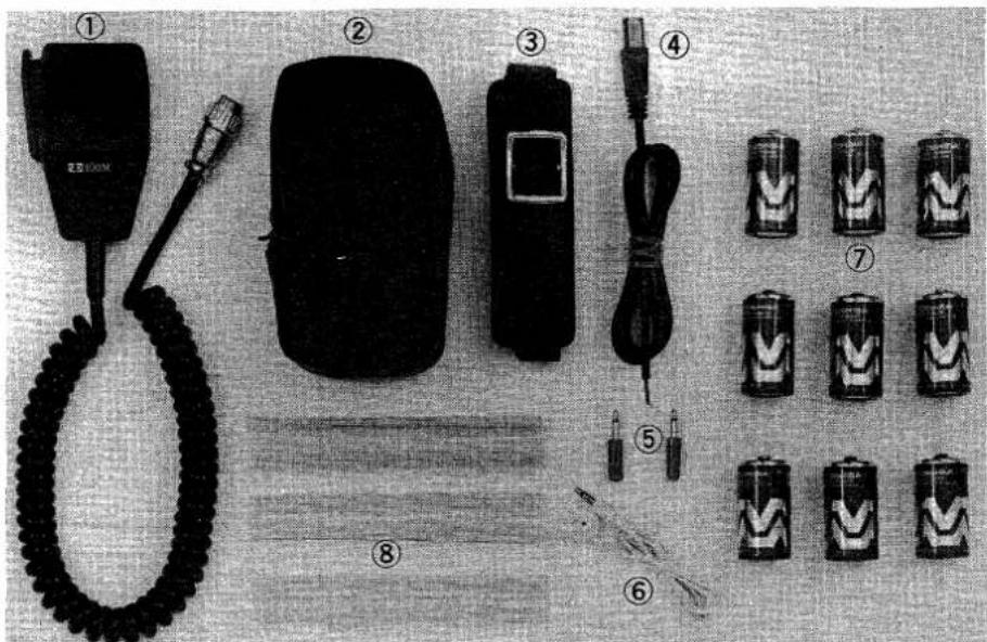
- Dynamic Microphone
1 5. Ext. Speaker Plug, Key Plug 2
- Microphone Case
1 6. Earphone 1
- Shoulder Strap
1 7. Dry Cells Type "C" 9
- Power Cord
1 8. Battery Tubes 3
natural_image
Diagram of a mechanical device with a curved component and directional arrows indicating motion (no text or symbols)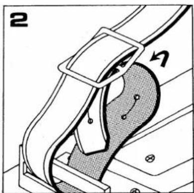
natural_image
Technical diagram of a mechanical component with no visible text or symbols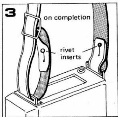
BATTERY INSTALLATION
Dry Batteries:
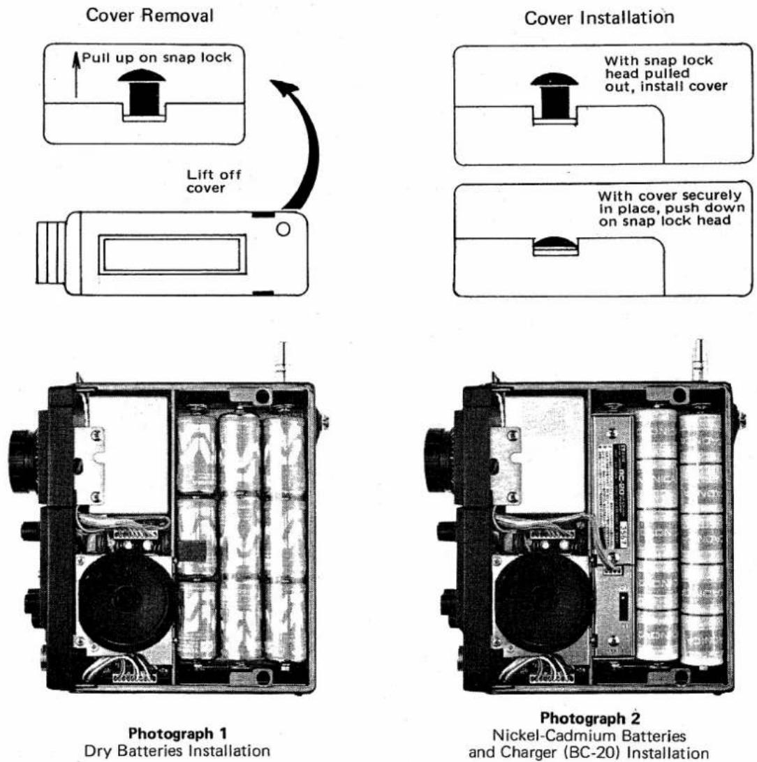
Place the mode switch in the OFF position. Remove the side that covers the battery case and speaker. Install the batteries into the battery tubes (three in each) taking care to observe the same direction (polarity).
Carefully install the battery tubes in the manner shown in photograph 1, placing the last three batteries in the inner column. Again take care to observe polarity, and place the battery tubes on top of the ribbon so when the batteries need to be removed, a simple pull on the ribbon will make removal easier. With the batteries properly in place, carefully replace the side cover.
Nickel-Cadmium Batteries and Charger: BC-20
First, install the charger in the battery case (the speaker side) of the transceiver housing as shown in photograph 2. The polarity of the switch end of the charger must be positive and on the case side, negative. Accordingly, the negative polarity must be connected to the spring side of the battery case.
Next, install five nickel-cadmium batteries in the battery tubes in the same direction. Make certain the (−) minus side is next to the spring. After installation of the charger and batteries in the case, connect the connector from the transceiver housing to the socket of the charger. Make sure the switch of the charger is ON, then install the side cover as before.
AC BATTERY CHARGER: BC-15
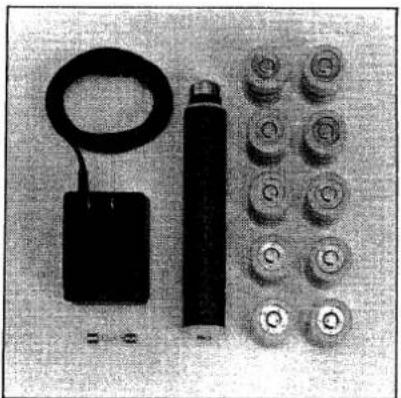
The BC-15 consists of an 117/220 Volt AC charger, 10 900mAh nickel-cadmium batteries, and a fuse box.
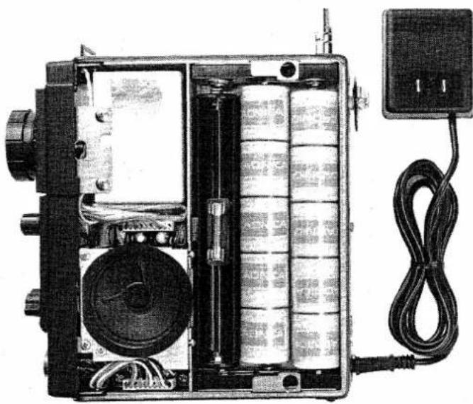
To install the BC-15 in the IC-502A, first put the Fuse Box into position, and then install the nickel-cadmium batteries in accordance with Photograph 3. After installation is completed, connect the output plug of the AC Adaptor to the External Power Supply Jack on the back of the IC-502A. For recharging, refer to the manual instructions for the AC adaptor.
After charging is completed, the batteries can be used in the same manner as dry cells. However, the voltage of nickel-cadmium batteries drops rapidly just before they are exhausted, so when the Power Indicator LED of the transceiver goes out, be sure to immediately stop using it, and charge the batteries again.
For use of the other sections, please refer to the charger instruction manual.
natural_image
Interior view of a portable electronic device with internal components and wiring (no visible text or symbols)Photograph 3
Nickel-Cadmium Batteries
and Charger (BC-15) Installation
WHEN TO REPLACE BATTERRIES
When the Power Indicator LED does not light up with the power switch ON, or when it lights up during reception and goes out during transmission, the batteries are exhausted. Use batteries of the same type, for mixed types might cause leakage. Replace worn batteries with a complete new set.
If used with old batteries, the life of new ones might be shortened. Battery life is shortened more by transmitting than by receiving, since several times more current is drawn in transmit. To prolong battery life, therefore, practice as follows:
* Try to minimize the transmit period.
* Reduce volume during reception.
* Be sure to cut off power source when set is not used.
More working hours are available if high-performance batteries such as Alkaline type are used.
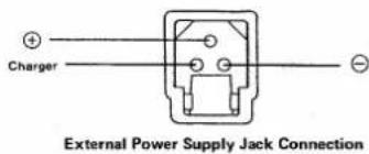
EXTERNAL POWER PLUG CONNECTION
External Power Source
For use at home or in the car, use an external power source which assures you of stable communication without concern about battery consumption.
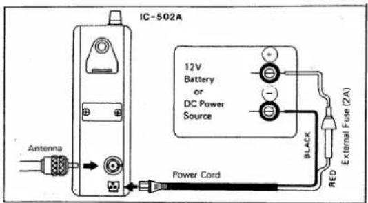
- Use either a regulated power supply or car battery of 13.8V DC and of over 1A current capability. (Though this transceiver may work at 11 to 15V DC, use it preferably at the rated voltage.)
- Correctly connect the external supply as shown in the figure. If polarity is reversed, source power is cut off by the protection circuit and the unit will not operate.
- When the transceiver is kept out of use for a prolonged period, the unit is operated for extended periods by external power only, or when the batteries are exhausted, etc., remove the batteries to protect the unit from possible damage by battery leakage.

FOR OUTDOOR USE
- Insert the supplied batteries. (Refer to "BATTERY INSTALLATION")
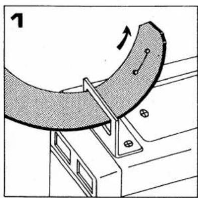
- Attach the supplied shoulder strap through the fixture of the body (as shown in the drawings on page 3).
- Fully extend the whip antenna for operation. Keep the collapsible antenna depressed when the set is not in use so that it will not be damaged.
FOR USE IN THE CAR
- Avoid using the unit near the outlet of heaters, air-conditioners, etc.
- Install the unit in a convenient place to avoid disrupting safe driving.
- For the best power source, connect to the car battery through a fuse (1A-2A).
- Firmly ground to the car body a mobile antenna (e.g. whip antenna), this is required.
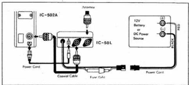
Cable Connection
Connection using I C-50 L
FOR FIXED USE
- Avoid installing the unit in places exposed to rain, water splash, direct sunshine, dust, vibration, or heat.
- An external antenna should be used for indoor operation. The use of the whip antenna indoors may cause TVI, BCI, Hi-Fi interference, malfunction of stabilized DC power supply, etc. When using an external antenna, be sure to collapse the telescoping antenna into the body.
- For fixed use, an external power supply is more economical than batteries.
- Use of the linear amplifier IC-50L, and AC power supply IC-3PS, give excellent performance for fixed use.
HOW TO USE EXTERNAL ANTENNA
Select a high performance antenna (a multi-element beam or gain antenna) and set it up in the highest possible position. Tightly connect the antenna so that performance will not be affected by weather or vibration. The matching impedance is designed to be 50 ohms.
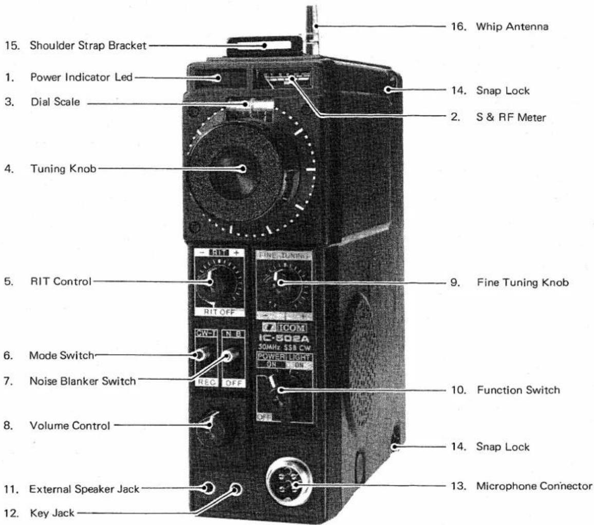
1. POWER INDICATOR LED
Shows when power is applied to the IC-502A and also indicates battery condition. When this LED is not illuminated with the power ON, the battery voltage is approximately 9.5V, or less.
2. S & RF METER
Indicates the relative signal strength of incoming signals and output power of transmitted signals.
3. DIAL SCALE
The dial is divided into 50 KHz increments with a total coverage of 1 MHz. The operating frequency is read on the dial.
4. TUNING KNOB
Tunes the frequency.
5. RIT
Independently swings the receiver frequency ± 3KHz so that signals that are slightly off frequency may be tuned for clarity without affecting the transmitting frequency.
6. MODE SWITCH
In the CW-T position the transmitter will transmit when the CW key makes contact. In the REC position both SSB and CW signals can be received. In the CW-T position the microphone is deactivated in the circuit.
7. NOISE BLANKER SWITCH
In the NB position, the noise blanker is put into the circuit and noise pulses will be reduced.
8. VOLUME
Controls the audio output level.
9. FINE TUNING
Tunes the operating frequency (both transmitting and receiving frequency) about ±2.5 KHz finely, so that you can find an exact receiving or transmitting frequency easily.
10. FUNCTION SWITCH
Turns the power ON and OFF and in the light position turns ON the meter light.
11. EXTERNAL SPEAKER JACK
An external speaker can be connected here. The impedance of the speaker should be 8 ohms. With the external speaker connected, the built-in speaker will be disabled.
12. KEY JACK
A key for CW transmission is connected here.
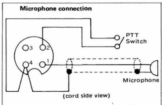
13. MICROPHONE CONNECTOR
A 600 ohm microphone is connected here.
14. SNAP LOCKS
Convenient snap-locks hold the sides in place. To remove them for any service or to replace the batteries, simply pull out on the center of the snap-lock and the cover can easily be removed. When replacing the covers be sure that you have placed the covers properly in the grooves provided, then push down on the center of the snap-lock. Note: At the time the sides are placed in the grooves, the snap-lock center must be pulled out.
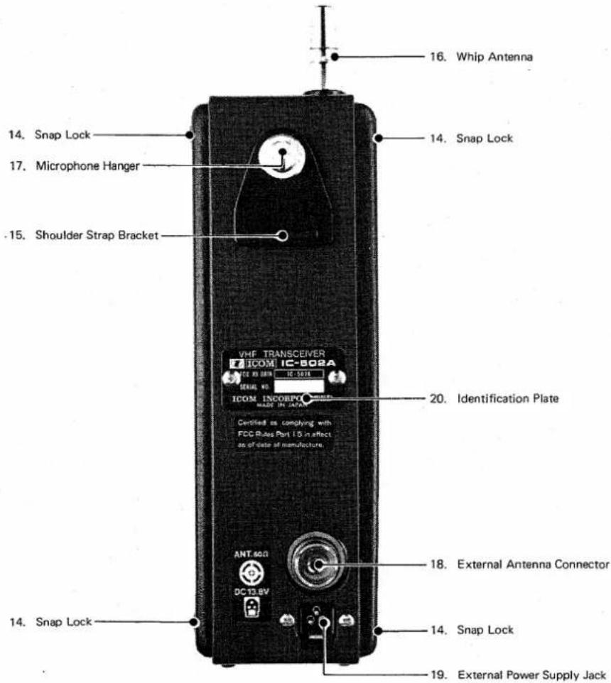
15. SHOULDER STRAP BRACKET
Connect the shoulder strap here for easy carrying. (See page 3)
16. WHIP ANTENNA
Extend completely for operation. When not in use, the antenna should be fully collapsed. Use care when extending or collapsing the antenna.
17. MICROPHONE HANGER
When not in use, the mike can be hung out of the way.
18. EXTERNAL ANTENNA RECEPTACLE
An external antenna of 50 ohms impedance can be connected here. If an external antenna is used, the built-in whip antenna should be completely collapsed.
19. EXTERNAL POWER SUPPLY JACK
Any well regulated power supply with an output of 13.8 volts can be connected here, instead of using the batteries installed. Inserting the power plug into the jack disables the internal battery source. When the BC-20 nicad battery pack is used, the external power source will charge the batteries.
20. IDENTIFICATION PLATE
Shows model number and serial number.
SECTION VI OPERATION
- After the batteries have been installed, or the IC-502A is connected to an external source, turn the function switch ON. If the surrounding light is too dim to see the S & SR meter, turn the switch to the LIGHT position, and the meter will be illuminated.
- Extend the whip antenna to its full length, or if you wish to use an external antenna, connect the cable to the EXT antenna connector on the back of the IC-502A.
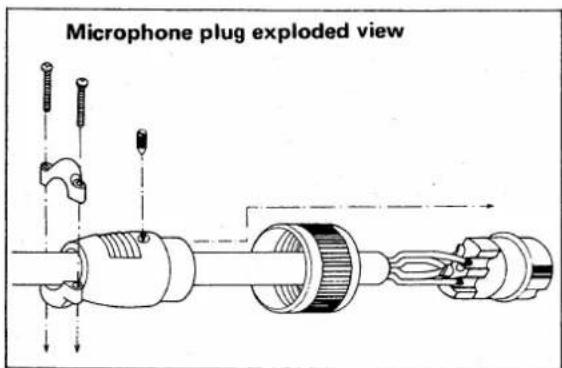
- Connect the microphone to the MIC connector on the front panel.
- If you wish to use the CW mode of transmission, connect a key to the KEY jack on the front panel. You do not have to disconnect the microphone for CW operation.
Key Wiring Diagram

-
Turn the tuning knob and the fine tuning knob until you reach the desired frequency or a signal is heard. Adjust the volume control for a comfortable level of listening. If operating SSB, you may wish to place the Noise Blanking switch in the NB position. This activates the noise blanking circuit which will suppress noise pulses. After selecting the operating frequency, if the received signal seems to drift, adjust the RIT control until the signal is again clear. Avoid adjusting the fine tuning knob for this purpose, as to do so will also change your transmitting frequency.
-
For SSB operation, hold the microphone close to your mouth, push the PTT switch on the microphone, and speak in a clear normal tone of voice. To receive release the PTT switch.
For CW operation, after connection of your KEY, place the Mode switch in the CW-T position and the IC-502A will transmit when the KEY contacts are closed. To receive, place the switch back in the REC position.
CIRCUITS
Section IX shows a block diagram of the IC-502A.
The receiving section is a single conversion superheterodyne with a 36MHz high-stability VFO as the local oscillator. The transmitting section is a single conversion system which employs a filter-type SSB generator using a 13.9985MHz crystal filter and the same local oscillator as the receiving section. A double-balanced mixer is used for the transmitting mixer to minimize spurious radiation. Although a portable unit, the IC-502A also features built-in circuits such as RIT, AGC, ALC, and an IF noise blanker.
The transceiver can be used with ease outdoors, in the car, or as a fixed station since it may be powered either with it's self-contained batteries (C size x 9) or with a 13.8VDC external source.
RECEIVING CIRCUIT
The signal from the whip antenna, or antenna terminal, passes through the harmonic filter, through the T/R switching diode D23 (M1301), amplified by RF amplifier Q2 (3SK74), and is then fed to the mixer Q3(2SK19) gate.
The switching diode is turned on by T/R control Q1 (2SA750), and D23 is turned on with forward voltage bias, thus directing the input signal to Q2. During transmission, the Receiver section +9V goes to zero turning off Q1, and forward voltage bias is not applied to D23, while at the same time, the transmit output is switched around Q2 to the antenna system. D23, is turned off as reverse bias is generated when the transmit signal is present.
The 36MHz local oscillator output from the VFO unit is injected to mixer Q3's source. The resultant conversion is an IF Frequency of 13.9985MHz. The IF signal passes through the diode switch D1(1SS53) which serves as both a transmit-receive switch and noise blanker gate. The IF selectivity is obtained by the 13.9985MHz crystal filter, then passes the switching diode D4(1SS53) and is amplified up to a suitable level by the IF amplifiers consisting of Q4(3SK74), Q5(3SK74) and IC1(BA401). The output of IC1 is applied to the detector and AGC circuits.
The detector circuit is a ring demodulator composed of D6 to D9(1N60's) which uses the 13.997 MHz from the BFO to generate the resultant audio signal. Higher audio frequencies of the de-modulated signal are cut off by a low-pass filter consisting of C46, L11 and C47.
The volume control (R3) adjusts this output level which is fed to AF amplifier IC2 ( PC575C2) providing 1 watt of audio. The network R5 and D1(1SS53) provides position bias to IC2 for muting audio during transmit and silent transmit-receive switching.
NOISE BLANKER
A sample of the IF signal is picked up at the drain of mixer Q3, amplified by IC2 and IC3 (BA 401's), and detected by D11(1N60). This detected output is separated into signal audio components, and pulse components (noise).
The signal component is amplified by Q6(2SC945) and provides AGC control of IC2. The noise pulse component turns on Q7(2SC945), and, as long as noise exists, turns off D1, by grounding the anode of the noise blanker gate diode D1, thus the noise component is not transferred to the crystal filter.
AGC CIRCUIT
A part of the IF signal is picked up from the IF amplifier IC1 and passes through C68 and R44 to be detected by D12, D13(1S2473's) and D14(1N60). When no signal is received, bias voltage is applied to the base of AGC control Q8(2SC945) through R43, D13 and D14, and the potential at the emitter of Q8 goes to nearly zero.
In the presence of a signal, C67, which is connected to Q8 base is first negatively charged because D13 is turned on, and so Q8 is turned off. Also, C66 which is connected to Q8 emitter is negatively charged through D12 up to a voltage determined by the loop gain of each amplifier of RF and IF, and C66 is kept at the achieved voltage due to the absence of a discharge circuit.
When the signal diminishes, the negative voltage charged in C67 is gradually discharged through R43 and drops down to a voltage where Q8 is turned on. Then, the negative voltage charged in C66 is rapidly discharged through Q8, thus the AGC time constant of fast attack and slow release is effected.
TRANSMITTING CIRCUIT
The small signal from the microphone is adjusted by the mike gain adjustment R17. Higher or lower frequencies outside desirable communication frequency range are attenuated by R19, C21 and C22, and the remaining frequencies are amplified by AF amplifier IC2(μPC566H). This AF signal and BFO output (13.997MHz) are fed to the balanced modulator IC4(SN76514N). The resulting carrier-suppressed double sideband signal is amplified by IF amplifier Q12(2SK49). The unwanted side band is then removed by the 13.9985MHz crystal filter where it passes through the diode switch D3(1SS53) to become a 13.9985MHz SSB(USB) signal.
This 13.9985MHz SSB(USB) signal passes the diode switch D2(1SS53) to the transmit mixer IC5 (SN76515N). The L.O. of 36MHz from the VFO unit is then combined to become the SSB(USB) signal of 50MHz. The transmit mixer IC5 is a double-balanced mixer, which minimizes spurious radiation.
In addition, the output circuits of IC5 and the 50MHz amplifier Q13(2SC383) provide a band-pass filtering which further minimizes spurious radiation. This 50MHz SSB signal is linearly amplified by Q14(2SC730) and Q15(2SC1947), respectively. Higher harmonics are suppressed by the low-pass filter composed of L25, L26 and C134 to C139. The resultant output power is 3W PEP. Q14 idling current is adjusted by R70. PA Q15 idling current is adjusted by R79. It is preset at 30mA at the factory.
ALC CIRCUIT
The ALC(Automatic Level Control) circuit picks out a part of the drive stage Q14 output, rectifies it by D19(1S2473) and D20(1N60), and applies the obtained negative voltage to the transmit IF amplifier Q12 gate, to control circuit gain. The ALC threshold level is adjusted by R73.
CW TRANSMISSION
For CW transmission, the voltage exerted on AF amplifier IC2 is reduced, at the same time. The voltage to BFO frequency shift switch Q9's(2SC945) base is also reduced, to turn it off so that C72 and C73 are in series as a part of th BFO crystal oscillator to shift the frequency about 1 KHz upward, which is within the crystal filter passband. Also, at this time, voltage is applied to the 5th pin of the balance modulator IC4 to upset carrier and the BFO frequency appears unsuppressed
at the output. Consequently, these signals are amplified by the transmit IF amplifier Q12, and pass through the crystal filter, transmit mixer IC5 and forward as in the SSB mode. Keying is done by
the Q12 source and Q13 emitter. The 800Hz signal is oscillated by the CR phase oscillator Q7 (2SC945) for the CW MONITOR, and fed to the AF oscillator ICI through the Volume Control.
COMMON CIRCUITS
BFO
The BFO is a Colpitts crystal-oscillator using Q10(2SC945). The crystal unit X1 has a load capacity of 25pF and operates at 13.997MHz in the SSB mode. The change in BFO Frequency is explained under "CW TRANSMISSION": The BFO output buffer is Q11(2SC945).
METER CIRCUIT
This circuit permits use of single meter as an S-meter during reception and as an output level meter during transmission.
A bridge circuit composed of R52 and R53 is connected to the power source, stabilized by Zener diode D6(WZ056), and the IF amplifier Q5 source. AGC voltage is generated by input signals reducing Q5's source voltage, thus unbalancing the bridge causing an upscale meter reading.
The S-meter is adjusted for its zero point by R53, and for its full scale point by R54. For the output level meter, the output detection diode D22(1N60) is coupled with L24 to partly rectify the RF output, thus giving an up-scale relative output indication.
The extent of the meter indication can be adjusted by changing the degree of coupling of D22 and L24.
POWER SOURCE AND TRANSMIT/RECEIVE CHANGE-OVER CIRCUIT
The power source voltage is 13.8V, supplied from either built-in batteries or external power connected to J2.
This voltage is directly applied to the AF power amplifier ICI in the receiver section, as well as to the collector of Q13, Q14, Q15 and IC5 in the power amplifier section.
Other circuits are fed with voltage from the voltage regulation circuits. The voltage regulator circuit for the VFO unit, BFO, and AGC circuits, is derived from 13.8V to the Zener diode D5 (XZ076), and the power-source indicating lamp D2 (light-emitting diode TLR-102), resulting in stabilized voltage of about 9.6V which becomes a reference level at D5's cathode. This voltage is applied to Q4's(2SC1209) base, and a regulated voltage of about 9V is available at its emitter.
The brightness of the power-indicating lamp varies according to the power voltage when the power voltage drops to a level under about 10V, the current to D5 and D2 stops, then D2 goes out. Thus the power voltage fluctuation, and battery condition, can be judged from the D2 display voltage regulator. For the receiving section regulated voltage supply the reference voltage of D5 cathode is applied to Q1(2SD355) base through D2(1SS53), and a regulated voltage of about 9.5V is obtained at its emitter.
When transmitting, R8 is grounded by the microphone PTT switch, or mode change-over switch (in the case of CW-T), to make Q1's base voltage zero and output voltage zero also. Likewise, for the transmit section regulated voltage, the reference voltage of D3 cathode is applied to Q3's (2SD355) base through D4(1SS53), and a regulated voltage of about 9.5V is obtained at its emitter.
During reception, since the PTT switch is not grounded, positive voltage is applied on the transmit/receive change-over control Q2(2SC945) base through R8 to turn on Q2, while the Q3 base is grounded through R13 and Q2, thus making the transmit voltage zero.
When transmitting, the PTT switch is grounded and the Q2 base is also grounded through D3 (1SS53) to turn off Q2 and apply the reference voltage to the Q3 base, and so a proper voltage is obtained. Also, the rise time for transmit/receive change-over is delayed by C13 and C14, respectively, to prevent transmission signals from entering the receiving section during the change-over operation.
RIT CONTROL AND FINE TUNING
When the RIT switch is turned ON in the receive mode, a positive voltage (R9V) is applied to the base of Q5 through the RIT switch and R26. Then Q5(2SC945) is turned on and Q6(2SC945) is turned off. So, a voltage divided by R3 in the VFO unit, and R4 the FINE TUNING, R2 the RIT CONTROL and R28 connected Q5 collector, is applied to a varactor diode D1(1S2688) in the VFO unit. Thus the VFO frequency (Receiving frequency) is adjustable by the FINE TUNING and the RIT CONTROL.
When the RIT switch is turned OFF in the receive mode and during transmit mode, the positive voltage at the base of Q5 goes to zero and as is turned off, and Q6 is turned on. So, a voltage divided by R3, and R4, R32 and R33, is applied to D1, and the VFO frequency is adjusted by the FINE TUNING only, thus the receiving frequency and the transmitting frequency are the same.
VFO UNIT
The oscillator circuit is a parallel tuned Colpitts circuit. Q1(2SK33) enables the oscillator frequency to be varied by changing the variable capacitor C2. In this oscillator, a range of 36MHz to 37MHz is produced and output is fed through to the buffer amplifiers Q2(2SK33), Q3(2SC710) and Q4(2SC710). The low-pass filter composed of L5 and L6, and C26, and C29 to C33, minimizes spurious radiation.
Though the regulated voltage for the oscillator is supplied at a level of about 9 volts from Q4 of the AMP unit, it is further stabilized by the constant current circuit using Q5(2SK19), and Zener diode D2(WZ056). This voltage is supplied to Q1, Q2, and RIT and FINE TUNING circuits to further ensure sufficient frequency stability.
In the RIT and FINE TUNING circuits, the capacitance of D1 is changed by voltage from R2 RIT control, and R4 FINE TUNING control, given through R1 and L2.C6 is connected in series, which keeps the RIT shift and FINE tune to approximately 2.5KHz each.
SECTION VIII MAINTENANCE AND ADJUSTMENT
ADJUSTMENT OF VARIOUS SECTIONS
This set is completely adjusted and checked so that it functions correctly. During prolonged use, however, the preadjusted condition may be affected by wear of parts, etc. If it is necessary to make adjustments at some time to regain specified performance, the following procedures may be followed.
Remember that changes in capacitor or coils will be very small, if any. Adjustments should not be attempted without adequate test equipment.
VFO UNIT ADJUSTMENT
1. Measuring Instruments for Adjustment:
* RF voltmeter (with about 1V full scale, capable of measuring at 51MHz)
* Frequency counter (capable of measuring 40MHz)
* Multimeter, 20K ohm per volt.
2. Frequency Adjustment:
Connect the frequency counter to J1 and J2 (ground side) of the Main unit.
Set the RIT and FINE TUNING knob to the center (12 o'clock) position.
Turn the tuning knob to set the dial scale to "51.0", and adjust trimmer C3 to obtain "37.000 MHz". Then set the dial scale to "50.0", and adjust L1 core to obtain "36.00MHz".
Repeat above adjustments as necessary until the end points are correct.
3. RIT Adjustment:
In the receive mode connect the frequency counter to J1 and J2 (ground side) of the Main unit, set the RIT knob to the center position, then record the frequency. (The dial scale and FINE TUNING knob may be set at any position, but do not change it during adjustment).
Next, turn the MODE switch to "CW-T" wihtout connecting a key to key jack, then read out the frequency. If it differs from the previously recorded frequency, adjust R33 on the AMP unit to equalize both frequencies.
Repeat above adjustments to reduce the frequency difference between reception and transmission to under 100Hz.
TRANSMITTING SECTION ADJUSTMENT
1. Measuring Instruments for Adjustment
* Terminal wattmeter (for about 10W full scale with 50ohm impedance)
* Frequency counter
* RF voltmeter
* AF oscillator
* AF millivoltmeter
* Multimeter 20K ohm per volt
2. Final Stage Idle Current Adjustment
Tune the MODE switch to "CW-T" without connecting a key to the key jack. Unsolder C129 and its lead, and connect the multimeter, which is set at 100mA range, between these points. Adjust R79 so that the current becomes 30mA.
After adjustment, resolder the lead of C129.
3. Coils Adjustment
Connect the wattmeter to the external antenna socket, and set the transmit/receive frequency at "50.5Hz".
With the MODE switch turned to "CW-T", connect a key to the key jack and hold the key down, connect the RF volt-meter probe to Q13 base and adjust the cores of L15 \~ L19 alternately for a maximum voltmeter reading.
4. Driving and Final Stage Adjustment
Make sure that the power voltage is 13.8V, under the same condition as in 3, then fully turn the R73 rotor toward ground and adjust L20, L21, C131 and C133 so that the watt meter indicates maximum (over 3W).
After this adjustment, adjust R73 so that the wattmeter indicates 3W.
Set multimeter to 1 volt range and connect to check point J12.
Readjust L15 \~ L19 cores for maximum indication.
5. RF Meter Adjustment
Move D22 with respect to L24(coupling) so that the meter indicates about 90% of full scale when the output is 3W at the completion of adjustment 4.
6. Carrier Frequency Adjustment
In the receive condition, connect the frequency counter to the R51 check-point, and adjust C71 so that the frequency becomes 13.997mHz. At this time, make sure that if the MODE switch is turned to "CW-T", the frequency shifts about 1KHz upward. Then turn the MODE switch to "REC" and connect the AF oscillator to Pin 6 of J13.
Ground microphone connector pin No.2 for SSB transmission, and set the AF oscillator oscillation frequency at 1.5KHz, and adjust the output level so that transmission output is 2.5W. Keeping this output level unchanged, alternately change the audio oscillator frequency from 300Hz to 3KHz, and fine adjust C71 to equalize the transmission outputs.
7. Mic Gain Adjustment
Connect the AF oscillator between microphone connector pins No.1 and No.4 (toward ground), and set its frequency at 1.5KHz, and output level at 6mV.
Ground pin No.2 and connect the AF millivoltmeter (300mV range) to the R24 check point and adjust R17 so that the meter reads 150mV.
This adjustment can be slightly changed depending on the use of microphone, strength of voice, condition of, etc. Observation of a high frequency oscilloscope, set to observe the output carrier, would be helpful while using normal microphone procedures, in order to achieve optimum waveform and quality.
RECEIVING SECTION ADJUSTMENT
1. Measuring Instruments for Adjustment
* Standard signal generator (for 50MHz band)
* AF millivoltmeter
* Multimeter
2. Sensitivity Adjustment
With the receiving frequency set at 50.5MHz and the volume knob in a reasonable volume position, connect the standard signal generator to the antenna connector and the AF millivoltmeter (1V range) to the AF output Pins No.1 and No.2 (toward ground) of J3.
3. S Meter Adjustment
Adjust R53 so that the S meter indicates zero in the non-signal condition. Next, with the signal generator output level set at 90dB() , adjust the frequency to the receiving frequency, and adjust R54 so that the S meter indicates full scale. After this adjustment is finished, lower the signal generator output level, and make sure that the signal generator output is within a range of 0dB ± 3dB when the S meter indicates S5.
4. Noise Blanker Adjustment
Set the signal generator output level at about 30dB ( V), and adjust the frequency to the receiving frequency. Making sure that beat is generated from the speaker, connect the multimeter (0.3V range) to R38 check-point, and gradually lower the signal generator output level, and adjust L12's core, to a point where the multimeter indication is maximum.
Never transmit during this adjustment because it might burn out the signal generator attenuators.
Keeping the standard signal generator unmodulated, set the output level at about 30dB ( V), and adjust the generator frequency to the receiving frequency. As a beat is heard from the speaker, fine-adjust the signal generator frequency, or receiving frequency, so that the beat becomes about 1000Hz. Try to keep the beat at this frequency during the adjustment.
Next, adjust L1 \~ L10 cores successively to maximize the AF millivoltmeter indication, and if the AF millivoltmeter becomes full-scale, lower the signal generator output level without converting the meter range or turning the volume knob, etc.
Repeat the adjustment until the AF millivoltmeter indicates over 800mV with the volume knob at maximum and S+N/N becomes over 10dB when the signal generator output level is -10dB ( V).
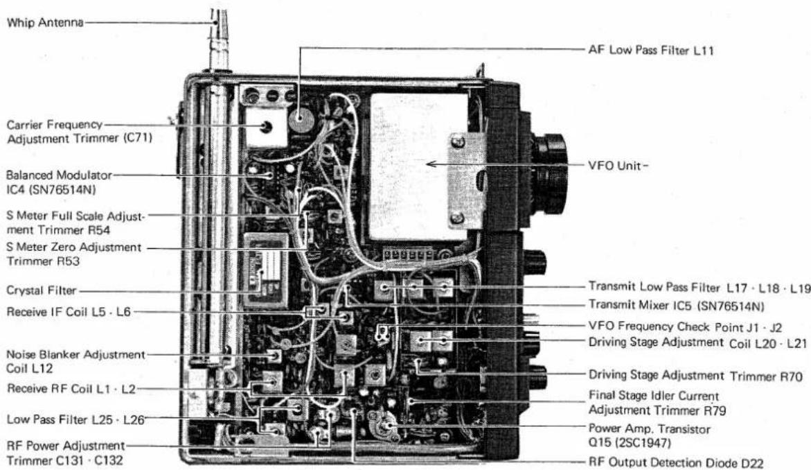
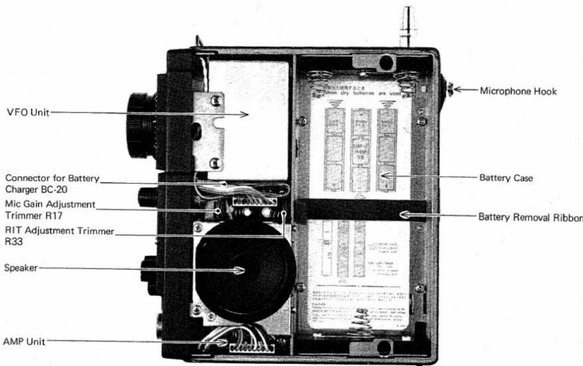
SECTION IX INSIDE VIEW
| Unit | Q No. | Mode | Transistor | FET | ||||||
| (B) | (C) | (E) | (G1) | (G2) | (D) | (S) | Remarks | |||
| Main | Q1 | R | 9 | 9.7 | 9.6 | NB-ON | ||||
| Q2 | R | 0 | 0.28 | 9 | 5 | |||||
| Q3 | T | 0 | 0 | 0.01 | ||||||
| Q3 | R | 0 | 9.2 | 1.15 | ||||||
| Q4 | T | 0 | 0.01 | 0.01 | 0 | |||||
| Q4 | R | 0 | 0.75 | 9.6 | 4.4 | |||||
| Q5 | T | 0 | 0.005 | 0.007 | 0.005 | |||||
| Q5 | R | 0 | 0.6 | 8.5 | 5.7 | |||||
| Q6 | T | 0 | 0.01 | E | ||||||
| Q6 | R | 0.002 | 1.35 | E | ||||||
| Q7 | T | 0 | 0.005 | E | ||||||
| Q7 | R | 0 | 6.3 | E | ||||||
| Q8 | T | 0.05 | E | 0 | ||||||
| Q8 | R | 0.05 | E | 0 | ||||||
| Q9 | T | 0.7 | 0.005 | E | ||||||
| Q9 | T | 0.7 | 0.005 | E | ||||||
| Q10 | T | 3.6 | 7.2 | 3.2 | ||||||
| Q10 | R | 3.6 | 7.2 | 3.2 | ||||||
| Q11 | T | 3.2 | 7.2 | 3.1 | ||||||
| Q11 | R | 3.2 | 7.2 | 3.1 | ||||||
| Q12 | T | 0 | 0.23 | 8.6 | ||||||
| Q12 | R | 0 | 0.005 | 0.01 | ||||||
| Q13 | T | 0.95 | 13.0 | 0.4 | ||||||
| Q13 | R | 0.005 | 13.8 | 0 | ||||||
| Q14 | T | 0.7 | 13.8 | E | ||||||
| Q14 | R | 0.01 | 13.8 | E | ||||||
| Q15 | T | 0.7 | 13.8 | E | ||||||
| Q15 | R | 0.005 | 13.8 | E | ||||||
| Q1 | T | 0.13 | 13.0 | 0.025 | CW-T | |||||
| Q1 | R | 11.0 | 13.5 | 9.7 | ||||||
| Q2 | T | 0.14 | 10.3 | E | CW-T | |||||
| Q2 | R | 0.7 | 0.045 | E | ||||||
| Q3 | T | 10.3 | 11.5 | 9.6 | CW-T | |||||
| Amp Unit | Q3 | R | 0.18 | 13.8 | 0.03 | |||||
| Q4 | T | 9.6 | 13.6 | 9 | CW-T | |||||
| Q4 | R | 9.6 | 13.5 | 9 | ||||||
| Q5 | T | 0 | 10.8 | E | CW-T | |||||
| Q5 | R | 0 | 10.8 | E | ||||||
| Q6 | T | 0.65 | 0 | E | CW-T | |||||
| Q6 | R | 0.65 | 0.005 | E | ||||||
| Q7 | T | 0.95 | 5.2 | 0 | CW-T | |||||
| VFO Unit | Q1 | R | 0 | 5.6 | 1.0 | |||||
| Q2 | R | 0 | 4.4 | 1.3 | ||||||
| Q3 | R | 3.5 | 9 | 2.9 | ||||||
| Q4 | R | 2.9 | 9 | 2.6 | ||||||
| Q5 | R | 5.6 | 9 | 6.0 | ||||||
| Unit | IC No. | Mode | Pin No. | Remarks | ||||||||||||
| 1 | 2 | 3 | 4 | 5 | 6 | 7 | 8 | 9 | 10 | 11 | 12 | 13 | 14 | |||
| Main Unit | IC1 | R | 1.35 | 1.35 | E | 9.2 | 9.2 | NB-ON | ||||||||
| IC2 | R | 1.35 | 1.35 | E | 8 | 8.6 | NB-ON | |||||||||
| IC-3 | R | 1.35 | 1.35 | E | 8.6 | 8.6 | ||||||||||
| IC-4 | T | 0 | 9.7 | 8.4 | 4.8 | 3.2 | E | E | E | 3.2 | 4.8 | 4.8 | 4.8 | 8.4 | E | |
| IC-5 | R | E | 12 | 10.4 | 6.2 | 0 | E | E | E | 4 | 6 | 6 | 6.2 | 10.4 | E | |
| IC-5 | T | E | 12 | 9.8 | 6.2 | 0 | E | E | E | 4 | 6 | 6 | 6.2 | 10.4 | E | |
| Amp Unit | IC-1 | R | 1.5 | 13.8 | 12.5 | 7.8 | 6.6 | 13.8 | 0.005 | 1.85 | CW-T | |||||
| IC-1 | T | 1.45 | 13.0 | 12.0 | 7.4 | 6.4 | 13.0 | 0.005 | 1.95 | |||||||
| IC-2 | T | 1.0 | 0.65 | 0.09 | E | 0.85 | 3.4 | 7.8 | ||||||||
Note: E = Ground
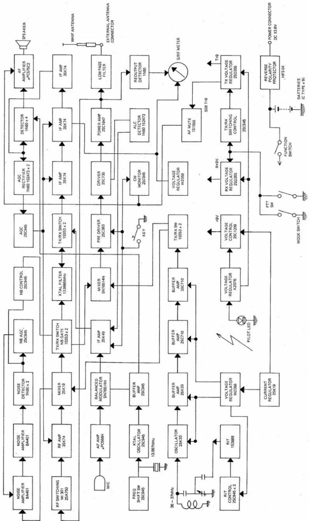
flowchart
graph TD
    A["NOISE AMPLIFIER BA401"] --> B["NOISE AMPLIFIER BA401"]
    B --> C["NOISE DETECTOR 1N60 x 2"]
    C --> D["NB AGC 25C945"]
    D --> E["NB CONTROL 25C945"]
    E --> F["AGC 25C945"]
    F --> G["AGC RECTIFIER 1N60 1S2473 x 2"]
    G --> H["DETECTOR 1N60 x 4"]
    H --> I["AF AMPLIFIER μPC575C2"]
    I --> J["Speaker"]

    K["RF SWITCHING MI 301 2SA750"] --> L["RF AMP 3SK74"]
    L --> M["MIXER 25K19"]
    M --> N["TX/RX SWITCH NB GATE 1SS53 x 2"]
    N --> O["XTAL FILTER 13.9985MHz"]
    O --> P["TX/RX SWITCH 1S553 x 2"]
    P --> Q["IF AMP 3SK74"]
    Q --> R["IF AMP 3SK74"]
    R --> S["IF AMP 3SK74"]

    T["MIC"] --> U["AF AMP μPC566H"]
    U --> V["BALANCED MODULATOR SN76514N"]
    V --> W["IF AMP 2SK49"]
    W --> X["MIXER SN76514N"]
    X --> Y["PREF DRIVER 2SC383"]
    Y --> Z["DRIVER 2SC730"]
    Z --> AA["POWER AMP 2SC1947"]
    AA --> AB["LOW PASS FILTER"]
    AB --> AC["S/RF METER"]

    AD["FREQ SHIFT SW 25C945"] --> AE["XTAL OSCILLATOR 2SC945"]
    AE --> AF["BUFFER AMP 2SC945"]
    AF --> AG["RESOLUT DETECTOR 1N60"]
    AG --> AH["S/RF METER"]

    AI["RIT CONTROL 2SC945 x 2"] --> AJ["VOLTAGE REGULATOR WZ056"]
    AJ --> AK["VOLTAGE REGULATOR XZ076"]
    AK --> AL["VOLTAGE REGULATOR 2SC1209"]
    AL --> AM["VOLTAGE REGULATOR 2SD355"]
    AM --> AN["TX/RX SWITCHING CONTROL"]
    AN --> AO["TX VOLTAGE REGULATOR 2SD355"]
    AO --> AP["T+9"]

    AQ["RIT 1S2688"] --> AR["VOLTAGE REGULATOR WZ056"]
    AR --> AS["VOLTAGE REGULATOR XZ076"]
    AS --> AT["VOLTAGE REGULATOR 2SC1209"]
    AT --> AU["VOLTAGE REGULATOR 2SD355"]
    AU --> AV["TX/RX SWITCHING CONTROL"]
    AV --> AW["TX VOLTAGE REGULATOR 2SD355"]
    AW --> AX["T+9"]

    AY["Pilot LED"] --> AZ["PILOT LED"]
    AZ --> BA["VOLTAGE REGULATOR WZ056"]
    BA --> BB["VOLTAGE REGULATOR XZ076"]
    BB --> BC["VOLTAGE REGULATOR 2SC1209"]
    BC --> BD["VOLTAGE REGULATOR 2SD355"]
    BD --> BE["TX/RX SWITCHING CONTROL"]
    BE --> BF["TX VOLTAGE REGULATOR 2SD355"]
    BF --> BG["T+9"]

    BH["MODE SWITCH"] --> BI["PTT SW"]
    BI --> BJ["FUNCTION SWITCH"]
    BJ --> BK["BATTERIES (C TYPE x 9)"]
    BK --> BL["HFS-04"]

    BM["REVERSE POLARITY PROTECTOR"] --> BN["POWER CONNECTOR DC 13.8V"]

    BO["WHIP ANTENNA"] --> BP["EXTERNAL ANTENNA CONNECTOR"]
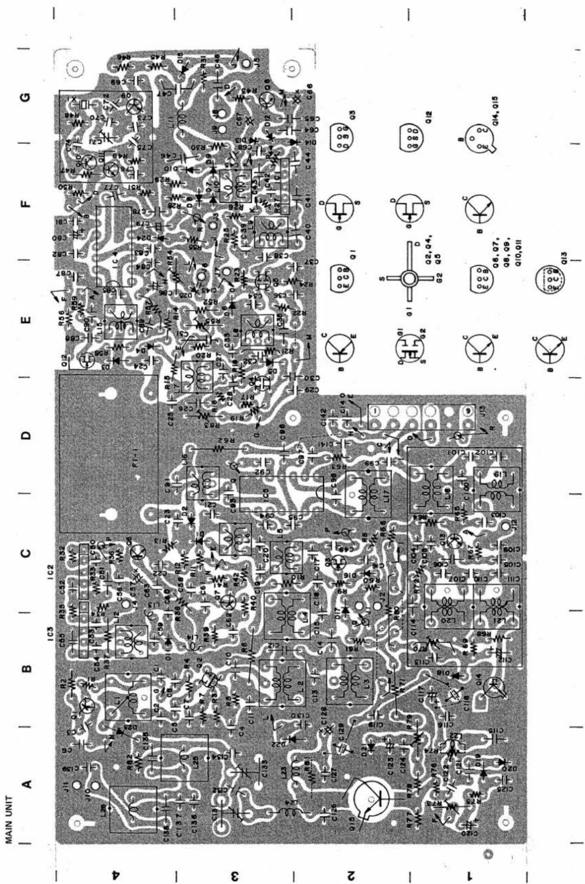
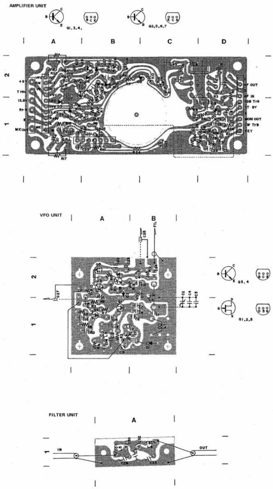
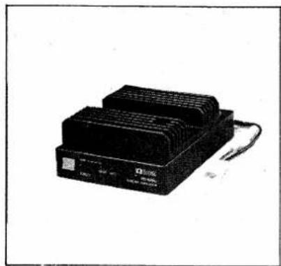
We have prepared a variety of options for the portable transceiver IC-502A in order to enlarge its use as a portable mobile and fixed set.
natural_image
Exterior view of a black electronic device with ventilation grilles and power cord (no visible text or symbols)IC-50L LINEAR AMPLIFIER 50MHz 10W
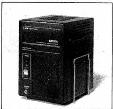
natural_image
Black-and-white photo of a desktop computer tower with visible drive bays and control panel (no text or labels)IC-3PS POWER SUPPLY 13.8V 3A
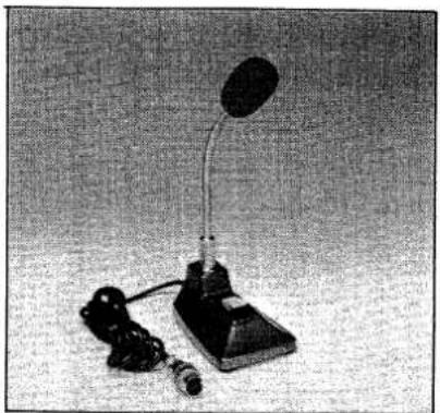
natural_image
Black-and-white photo of a desk lamp with adjustable arm and bulb, no visible text or symbolsIC-SM2 DESK MICROPHONE ELECTRET CONDENSER TYPE
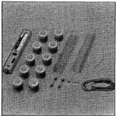
natural_image
Assorted mechanical components including rollers, a ruler, and a coiled spring on a textured surface (no visible text or symbols)RECHARGEABLE BATTERY PACK BATTERY CHARGER BC-20 BATTERY N-900 x 10 (900mAh)
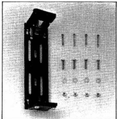
natural_image
Black mechanical component with multiple bolts arranged in a grid pattern (no visible text or symbols)MOBILE MOUNTING BRACKET IC-MB2 FOR IC-502A
natural_image
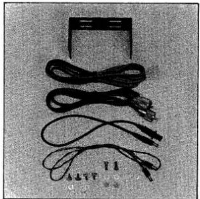
Black-and-white photo of multiple black cable bundles arranged in a row, with no visible text or symbols.MOBILE MOUNTING KIT FOR IC-50L
natural_image
Collection of electronic components including a battery, coil, and multiple cylindrical pins (no visible text or symbols)RECHARGEABLE BATTERY PACK AC BATTERY CHARGER BC-15 BATTERY N-900C x 10 (900mAh)

natural_image
Close-up of a textured fabric with uniform gray bands and a vertical dark band on the right (no text or symbols)ICOM INCORPORATED
1-6-19, Kami Kuratsukuri, Hirano-ku, Osaka, Japan

natural_image
Close-up of a textured gray surface with a vertical dark band on the right side (no text or symbols)- IC-502A
- METER SSB PORTABLE TRANSCEIVER
- TABLE OF CONTENTS
- SECTION I SPECIFICATIONS
- SECTION III ACCESSORIES
- BATTERY INSTALLATION
- AC BATTERY CHARGER: BC-15
- WHEN TO REPLACE BATTERRIES
- EXTERNAL POWER PLUG CONNECTION
- External Power Source
- FOR OUTDOOR USE
- FOR USE IN THE CAR
- FOR FIXED USE
- HOW TO USE EXTERNAL ANTENNA
- POWER INDICATOR LED
- S & RF METER
- DIAL SCALE
- TUNING KNOB
- RIT
- MODE SWITCH
- NOISE BLANKER SWITCH
- VOLUME
- FINE TUNING
- FUNCTION SWITCH
- EXTERNAL SPEAKER JACK
- KEY JACK
- MICROPHONE CONNECTOR
- SNAP LOCKS
- SHOULDER STRAP BRACKET
- WHIP ANTENNA
- MICROPHONE HANGER
- EXTERNAL ANTENNA RECEPTACLE
- EXTERNAL POWER SUPPLY JACK
- IDENTIFICATION PLATE
- SECTION VI OPERATION
- CIRCUITS
- RECEIVING CIRCUIT
- NOISE BLANKER
- AGC CIRCUIT
- TRANSMITTING CIRCUIT
- ALC CIRCUIT
- CW TRANSMISSION
- COMMON CIRCUITS
- BFO
- METER CIRCUIT
- POWER SOURCE AND TRANSMIT/RECEIVE CHANGE-OVER CIRCUIT
- RIT CONTROL AND FINE TUNING
- VFO UNIT
- SECTION VIII MAINTENANCE AND ADJUSTMENT
- ADJUSTMENT OF VARIOUS SECTIONS
- VFO UNIT ADJUSTMENT
- Measuring Instruments for Adjustment:
- Frequency Adjustment:
- RIT Adjustment:
- TRANSMITTING SECTION ADJUSTMENT
- Measuring Instruments for Adjustment
- Final Stage Idle Current Adjustment
- Coils Adjustment
- Driving and Final Stage Adjustment
- RF Meter Adjustment
- Carrier Frequency Adjustment
- Mic Gain Adjustment
- RECEIVING SECTION ADJUSTMENT
- Sensitivity Adjustment
- S Meter Adjustment
- Noise Blanker Adjustment
- SECTION IX INSIDE VIEW
- ICOM INCORPORATED
Marke : ICOM
Modell : IC-502A
Kategorie : Empfänger